Silicon Laboratories Finland WT41 WT41 Bluetooth Module User Manual Product Data Sheet
Silicon Laboratories Finland Oy WT41 Bluetooth Module Product Data Sheet
Contents
manual

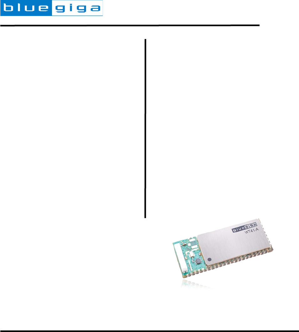
WT41-A / WT41-N
DATA SHEET
Thursday, 10 March 2011
Version 1.2
Bluegiga Technologies Oy
Copyright © 2000-2011 Bluegiga Technologies
All rights reserved.
Bluegiga Technologies assumes no responsibility for any errors which may appear in this manual.
Furthermore, Bluegiga Technologies reserves the right to alter the hardware, software, and/or specifications
detailed here at any time without notice and does not make any commitment to update the information
contained here. Bluegiga’s products are not authorized for use as critical components in life support devices
or systems.
The WRAP is a registered trademark of Bluegiga Technologies
The Bluetooth trademark is owned by the Bluetooth SIG Inc., USA and is licensed to Bluegiga Technologies.
All other trademarks listed herein are owned by their respective owners.

Bluegiga Technologies Oy
VERSION HISTORY
Version Comment
0.1 First draft
0.2 Description and product codes added
0.21 Dimensions updated, layout guide added, UART and USB chapters added
0.22 Pin descriptions, PCM, USB, UART, SPI
0.3 Physical dimensions corrected
0.31 Product codes corrected
0.32 Recommendation for a power-up reset circuitry added to chapter 10
0.4 Pins 1 and 52 (GND) removed. Dimensions updated, recommended land
pattern added
0.5 Certification information added
0.6 Physical dimensions and recommended PCB land pattern updated
0.7 Figure 5 recommended land pattern corrected
1.0 Radio and antenna characteristics, layout guide for WT41-N
1.1 Japan certification info added
1.2 FCC RF radiation exposure statement updated
Bluegiga Technologies Oy
TABLE OF CONTENTS
1 Ordering Information......................................................................................................................................7
2 Pinout and Terminal Description ...................................................................................................................8
3 Electrical Characteristics ............................................................................................................................ 11
3.1 Absolute Maximum Ratings ................................................................................................................ 11
3.2 Recommended Operating Conditions ................................................................................................. 11
3.3 Transmitter Performance For BDR ..................................................................................................... 11
3.4 Radiated Spurious Emissions ............................................................................................................. 12
3.5 Receiver Performance ........................................................................................................................ 13
3.6 Current Consumption .......................................................................................................................... 13
3.7 Antenna Performance and Radiation Patterns ................................................................................... 14
4 Physical Dimensions .................................................................................................................................. 18
5 Layout Guidelines ....................................................................................................................................... 20
5.1 WT41-A ............................................................................................................................................... 20
5.2 WT41-N ............................................................................................................................................... 20
5.2.1 Layout for WT41-N with u.fl connector close to RF pin ............................................................... 20
5.2.2 Layout for WT41-N with 50 ohm trace from RF pin to a SMA connector .................................... 21
6 UART Interface ........................................................................................................................................... 23
6.1 UART Bypass ...................................................................................................................................... 25
6.2 UART Configuration While Reset is Active ......................................................................................... 25
6.3 UART Bypass Mode ............................................................................................................................ 25
7 USB Interface ............................................................................................................................................. 26
7.1 USB Data Connections ....................................................................................................................... 26
7.2 USB Pull-Up resistor ........................................................................................................................... 26
7.3 USB Power Supply .............................................................................................................................. 26
7.4 Self-Powered Mode ............................................................................................................................. 26
7.5 Bus-Powered Mode ............................................................................................................................. 27
7.6 USB Suspend Current ......................................................................................................................... 28
7.7 USB Detach and Wake-Up Signaling.................................................................................................. 28
7.8 USB Driver .......................................................................................................................................... 29
7.9 USB v2.0 Compliance and Compatibility ............................................................................................ 29
8 Serial Peripheral Interface (SPI) ................................................................................................................. 30
9 PCM Codec Interface ................................................................................................................................. 31
9.1 PCM Interface Master/Slave ............................................................................................................... 31
9.2 Long Frame Sync ................................................................................................................................ 32
9.3 Short Frame Sync ............................................................................................................................... 32
9.4 Multi-slot Operation ............................................................................................................................. 33
Bluegiga Technologies Oy
9.5 GCI Interface ....................................................................................................................................... 33
9.6 Slots and Sample Formats .................................................................................................................. 34
9.7 Additional Features ............................................................................................................................. 35
9.8 PCM_CLK and PCM_SYNC Generation ............................................................................................ 35
9.9 PCM Configuration .............................................................................................................................. 36
10 I/O Parallel Ports ..................................................................................................................................... 38
10.1 PIO Defaults ................................................................................................................................. 38
11 Reset ....................................................................................................................................................... 39
11.1 Pin States on Reset ..................................................................................................................... 40
12 Certifications ........................................................................................................................................... 41
12.1 Bluetooth ...................................................................................................................................... 41
12.2 FCC .............................................................................................................................................. 41
12.3 CE ................................................................................................................................................ 42
12.4 Industry Canada (IC) .................................................................................................................... 42
12.5 Japan ........................................................................................................................................... 42
12.6 Qualified Antenna Types for WT41-N .......................................................................................... 42
13 Contact Information................................................................................................................................. 43
Bluegiga Technologies Oy
WT41 Bluetooth® Module
DESCRIPTION
WT41 is a long range class 1, Bluetooth® 2.1 +
EDR module. WT41 is a highly integrated and
sophisticated Bluetooth® module, containing all the
necessary elements from Bluetooth® radio to
antenna and a fully implemented protocol stack.
Therefore WT41 provides an ideal solution for
developers who want to integrate Bluetooth®
wireless technology into their design with limited
knowledge of Bluetooth® and RF technologies.
WT41 is optimized for long range applications and
since it contains a RF power amplifier, low noise
amplifier and a highly efficient chip antenna. With
115 dB radio budget WT41 can reach over 1 km
range in line off sight.
By default WT41 module is equipped with powerful
and easy-to-use iWRAP firmware. iWRAP enables
users to access Bluetooth® functionality with simple
ASCII commands delivered to the module over
serial interface - it's just like a Bluetooth® modem.
APPLICATIONS:
• Hand held terminals
• Industrial devices
• Point-of-Sale systems
• PCs
• Personal Digital Assistants (PDAs)
• Computer Accessories
• Access Points
• Automotive Diagnostics Units
FEATURES:
• Fully Qualified Bluetooth v2.1 + EDR end
product, CE and FCC and IC
• TX power : 19 dBm
• RX sensitivity : -92 dBm
• Higly efficient chip antenna, U.FL connector or
RF pin
• Class 1, range up to 800 meters
• Industrial temperature range from -40oC to
+85oC
• RoHS Compliant
• USB interface (USB 2.0 compatible)
• UART with bypass mode
• 6 x GPIO
• 1 x 8-bit AIO
• Support for 802.11 Coexistence
• Integrated iWRAPTM Bluetooth stack or HCI
firmware

Bluegiga Technologies Oy
Page 7 of 43
1 Ordering Information
Product series
Firmware
HCI = HCI firmware (Bluetooth 2.0 + EDR)
HCI21= HCI firmware (Bluetooth 2.1 + EDR)
HCI30= HCI firmware (Bluetooth 3.0)
AI = iWRAP 2.2.0
AI3 = iWRAP 3.0.0
AI4 = iWRAP 4.0.0
HW version
A = Chip antenna
N = RF pin
WT41-A-HCI
Bluegiga Technologies Oy
Page 8 of 43
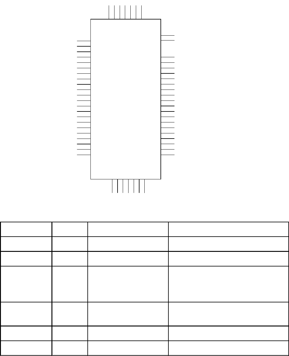
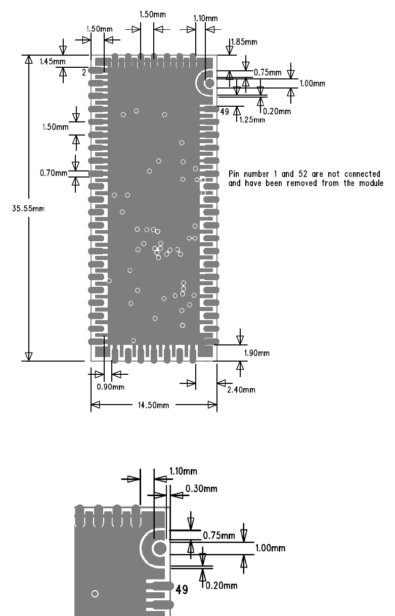
2 Pinout and Terminal Description
Pins 1 and 52 (GND)
are not connected
and have been
removed
2
3
4
5
6
7
8
9
10
11
12
13
14
15
16
17
18
19
20
21
22
23
24
25
26
27
28
29
51
49
48
47
46
45
44
43
42
41
40
39
38
37
36
35
34
33
32
31
30
59
58
57
56
55
54
53
GND
GND
GND
GND
GND
GND
GND
GND
GND
GND
GND
GND
GND
GND
GND
GND
RFGND
RF
GND
GND
GND
GND
GND
GND
VDD_PA
PIO2
PIO3
UART_RTS
UART_RX
GND
USB+
USB-
UART_CTS
PCM_IN
PCM_CLK
PCM_SYNC
GND
GND
GND
GND
GND
GND
PCM_OUT
PIO4
GND
VDD
RESET
PIO6
PIO7
GND
SPI_CSB
SPI_CLK
SPI_MISO
SPI_MOSI
PIO5
UART_TX
AIO
50
Figure 1: WT41 pin out
PIN
NUMBER
PAD TYPE DESCRIPTION
NC 1, 52 Not connected
Pins 1 and 52 (GND) have been removed
from the module.
RESET 33
Input, weak internal pull-
up
Active low reset. Keep low for >5 ms
to cause a reset
GND
2-10, 16,
23,24,26-
28, 30,
31,36,44-
49, 53-59
GND GND
RF 51 RF output
RF output for WT41-N. For WT41-A
and WT41-E this pin is not connected
RFGND 50 GND
RF ground. Connected to GND internally to
the module.
VDD_PA 11 Supply voltage
Supply voltage for the RF power amplifier
and the low noise amplifier of the module
Table 1: Supply and RF Terminal Descriptions

Bluegiga Technologies Oy
Page 9 of 43
PIO PORT PIN
NUMBER PAD TYPE DESCRIPTION
PIO[2] 12 Bi-directional, programmamble
strength internal pull-down/pull-up Programmamble input/output
line
PIO[3] 13 Bi-directional, programmamble
strength internal pull-down/pull-up Programmamble input/output
line
PIO[4] 29 Bi-directional, programmamble
strength internal pull-down/pull-up Programmamble input/output
line
PIO[5] 41 Bi-directional, programmamble
strength internal pull-down/pull-up Programmamble input/output
line
PIO[6] 34 Bi-directional, programmamble
strength internal pull-down/pull-up Programmamble input/output
line
PIO[7] 35 Bi-directional, programmamble
strength internal pull-down/pull-up Programmamble input/output
line
AIO[1] 43 Bi-directional
Programmamble analog
input/output line
Table 2: GPIO Terminal Descriptions
SPI
INTERFACE
PIN
NUMBER
PAD TYPE DESCRIPTION
PCM_OUT 25
CMOS output, tri-state,
weak internal pull-down
Synchronous data output
PCM_IN 20
CMOS input, weak
internal pull-down
Synchronous data input
PCM_SYNC 22
Bi-directional, weak
internal pull-down
Synchronous data sync
PCM_CLK 21
Bi-directional, weak
internal pull-down
Synchronous data clock
Table 3: PCM Terminal Descriptions
UART
Interfaces
PIN
NUMBER
PAD TYPE DESCRIPTION
UART_TX 42
CMOS output, tri-
state, with weak
internal pull-up
UART data output, active high
UART_RTS# 14
CMOS output, tri-
state, with weak
internal pull-up
UART request to send, active low
UART_RX 15
CMOS input, tri-
state, with weak
internal pull-down
UART data input, active high
UART_CTS# 19
CMOS input, tri-
state, with weak
internal pull-down
UART clear to send, active low
Table 4: UART Terminal Descriptions

Bluegiga Technologies Oy
Page 10 of 43
USB Interfaces
PIN
NUMBER
PAD TYPE DESCRIPTION
USB+ 17 Bidirectional
USB data plus with selectable internal 1.5k
pull-up resistor
USB- 18 Bidirectional USB data minus
Table 5: USB Terminal Descriptions
SPI
INTERFACE
PIN
NUMBER
PAD TYPE DESCRIPTION
SPI_MOSI 40
CMOS input with weak
internal pull-down
SPI data input
SPI_CS# 37
CMOS input with weak
internal pull-up
Chip select for Serial Peripheral
Interface, active low
SPI_CLK 38
CMOS input with weak
internal pull-down
SPI clock
SPI_MISO 39
CMOS output, tristate,
with weak internal pull
down
SPI data output
Table 6: Terminal Descriptions
Bluegiga Technologies Oy
Page 11 of 43
3 Electrical Characteristics
3.1 Absolute Maximum Ratings
Min Max Unit
-40 85 °C
-0.4 3.6 V
VSS-0.4 VDD+0.4 V
Rating
Storage Temperature
Other Terminal Voltages
VDD_PA, VDD
Table 7: Absolute Maximum Ratings
3.2 Recommended Operating Conditions
Min Max Unit
-40 85 °C
3.0 3.6 V
Rating
Operating Temperature Range
VDD_PA, VDD *)
*) VDD_PA has an effect on the RF output power.
Table 8: Recommended Operating Conditions
3.3 Transmitter Performance For BDR
Antenna gain 2.3dBi taken into account
Min Typ Max
Bluetooth
Specification
Unit
17 19 20 20 dBm
4 - dB
1.5 -dB
0.1 1 2 - dB
-10 19
942 1000 kHz
F = F
0
± 2MHz -20 -20
F = F
0
± 3MHz -40 -40
F = F
0
> 3MHz -40 -40
7+/-25 kHz
169 140<175 kHz
161 140<175 kHz
1.1 >=0.8
20dB band width for modulated carrier
ΔF1
max
ΔF
1avg
RF power variation over supply voltage range (*
RF Characetristics, VDD = 3.3V @ room
temperature unless otherwise specified
Drift rate
ΔF
2avg
/ ΔF
1avg
ACP (1
maximum RF Transmit Power
RF power variation over temperature range
RF power variation over BT band
RF power control range (*
Table 9: Transmitter performance for BDR

Bluegiga Technologies Oy
Page 12 of 43
3.4 Radiated Spurious Emissions
Measured from WT41 evaluation board
Standard Band / Frequency
Min
(AVG /
PEAK)
Typ
(AVG /
PEAK)
Max
(AVG /
PEAK)
Limit by the Standard
(AVG / PEAK)
Unit
2nd harmonic 52 54/58 54 / 74 dBuV/m
3rd harmonic 51 54/58 54 / 74 dBuV/m
Band edge
2390MHz
50/60 52/63
54 / 74 dBuV/m
Band edge
2483.5MHz
52/65 54/67
54 / 74 dBuV/m
Band edge
2400MHz
(conducted)
-50
-20 dBc
Band edge
2483.5MHz
(conducted)
-58 -20 dBc
Band edge
2400MHz
-39 -36 -30
dBm
2nd harmonic -41 -30
dBm
3rd harmonic -41 -30
dBm
(2400 - 2479) MHz -
-47 dBm
(1600 - 1653) MHz -52 -47 dBm
ETSI EN 300 328
transmitter
spurious
emissions
FCC part 15
transmitter
spurious
emissions
ETSI EN 300 328
receiver spurious
Table 10:Radiated spurious emission for WT41-A
Standard
Min
(AVG /
PEAK)
Typ (AVG
/ PEAK)
Max
(AVG /
PEAK)
Limit by the Standard
(AVG / PEAK)
Unit
2nd harmonic <48/55 50/56 54 / 74 dBuV/m
3rd harmonic <48/51 48/52 54 / 74 dBuV/m
Band edge
2390MHz
50/60 52/63
54 / 74 dBuV/m
Band edge
2483.5MHz
52/65 54/67
54 / 74 dBuV/m
Band edge 2400
MHz (conducted)
-50
-20 dBc
Band edge
3483.5MHz
(conducted)
-58 -20
dBc
Band edge
2400MHz
-39 -36 -30
dBm
2nd harmonic -30
dBm
3rd harmonic -30
dBm
(2400 - 2479) MHz
-47 dBm
(1600 - 1653) MHz -47 dBm
ETSI EN 300 328
transmitter
spurious emissions
FCC part 15
transmitter
spurious emissions
ETSI EN 300 328
receiver spurious
Table 11: Radiated spurious emission for WT41-N
Bluegiga Technologies Oy
Page 13 of 43
3.5 Receiver Performance
Antenna gain not taken into account
RF characteristis, VDD = 3.3V,
room temperature (**
Packet type Min Typ Max
Bluetooth
Spefication
Unit
DH1 -92 -70 dBm
DH3 -92 dBm
DH5 -91 dBm
2-DH1 -94 dBm
2-DH3 -93 dBm
2-DH5 -93 dBm
3-DH1 -88 dBm
3-DH3 -85 dBm
3-DH5 -84 dBm
Sensitivity variation over
temperature range
TBD
Sensitivity for 0.1% BER
Table 12: Receiver sensitivity
3.6 Current Consumption
Peak (mA) AVG (mA)
-2.1
100.5 77.6
99.3 77.6
98.1 71.1
98.1 71.2
98.7 51.6
164 120
166 67.3
56.8 52.6
0.36
169.3 58.7
RX
Inquiry
Deep sleep
TX 2DH1
TX DH5
Opearation mode
TX 3DH5
TX 2DH5
TX 3DH3
TX 2DH3
TX DH1
Stand-by, page mode 0
Table 13: Current consumption
Bluegiga Technologies Oy
Page 14 of 43
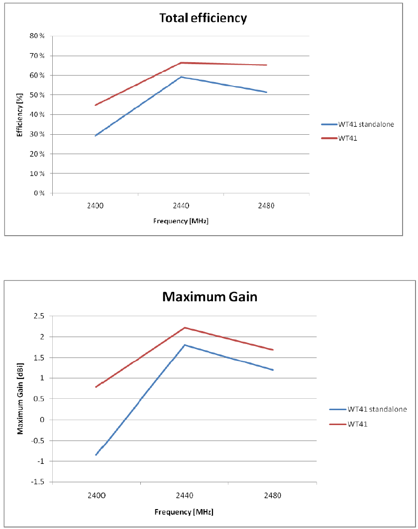
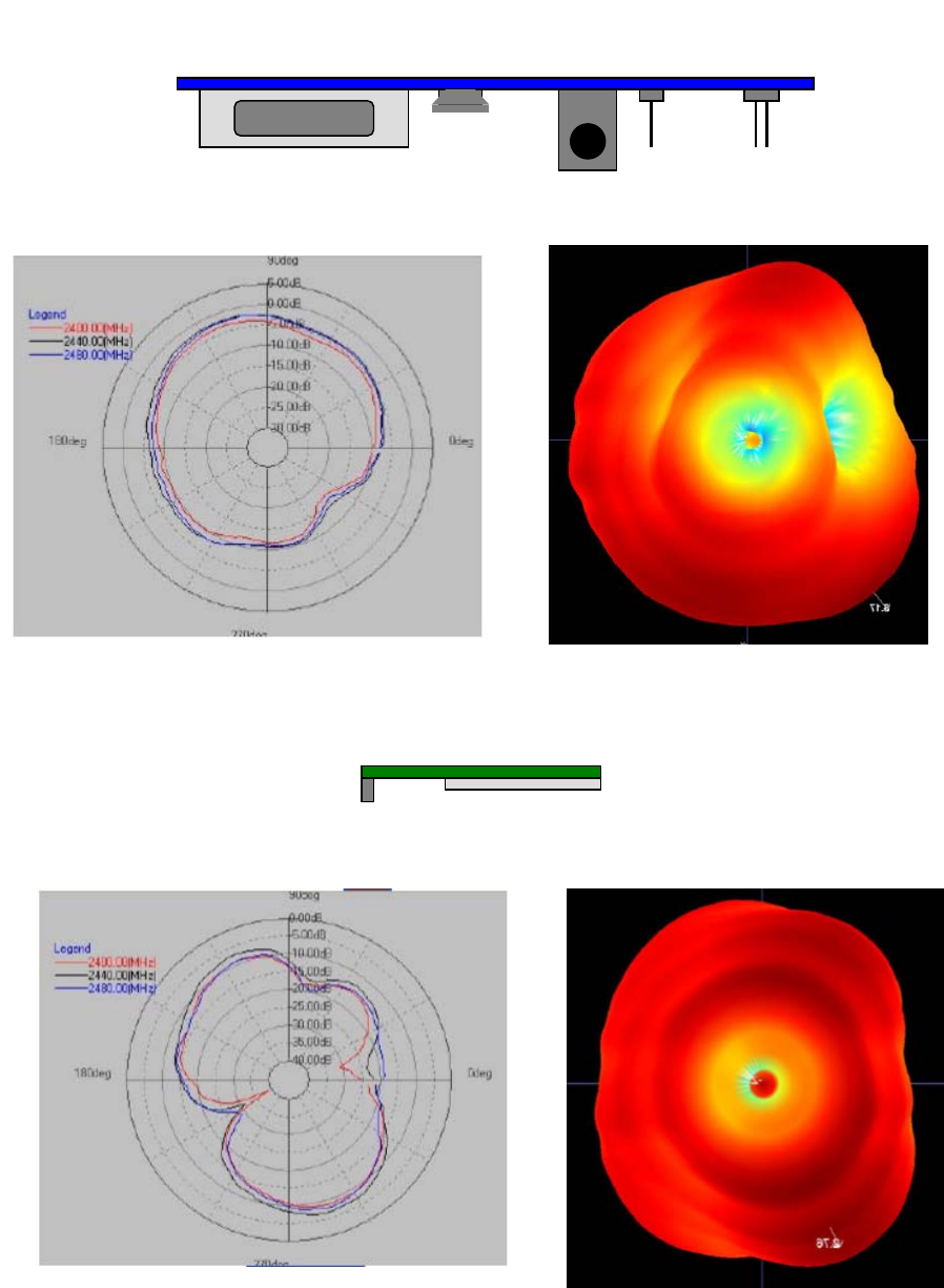
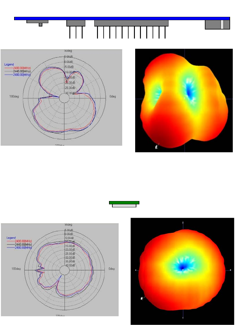
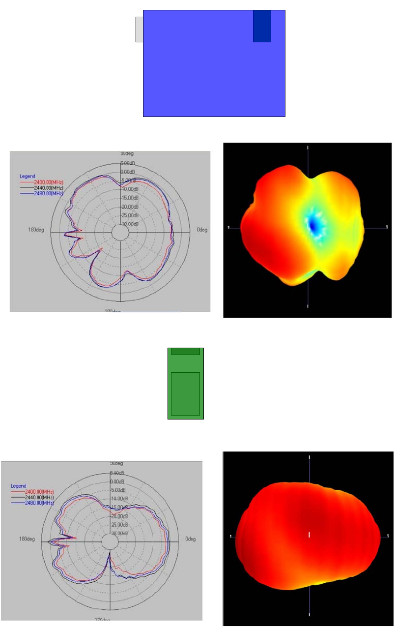
3.7 Antenna Performance and Radiation Patterns
Antenna performance measured from the module as a standalone and as mounted to the evaluation board.
Table 14: Total efficiency of the chip antenna
Table 15:Peak gain of the chip antenna
Bluegiga Technologies Oy
Page 15 of 43
WT41 Evaluation Board
WT41 stand alone
Bluegiga Technologies Oy
Page 16 of 43
WT41 Evaluation Board
WT41 stand alone
Bluegiga Technologies Oy
Page 17 of 43
Back side of the
evaluation kit
Back side of
WT41-A
Bluegiga Technologies Oy
Page 18 of 43
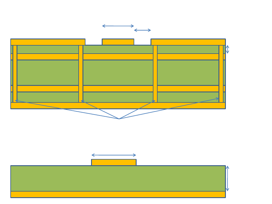
4 Physical Dimensions
Figure 2: Physical dimensions (top view)
Figure 3: Dimensions for the RF pin (top view)
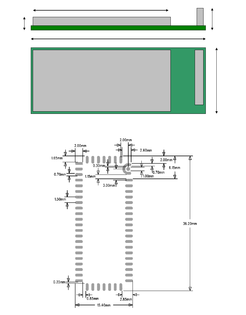
Bluegiga Technologies Oy
Page 19 of 43
3.35 mm
35.3 mm
5.65 mm
25.3 mm
14.0 mm
Figure 4: Dimensions of WT41
Figure 5: Recommended land pattern
Bluegiga Technologies Oy
Page 20 of 43
5 Layout Guidelines
5.1 WT41-A
WT41-A should be mounted directly over a solid GND plane. The best performance can be achieved when
placing the module to the left corner or to a middle edge of the mother board, as shown in the figure below.
Components can be mounted directly under the module and the antenna. The antenna is extremely robust for
environment in close proximity to the antenna. Any dielectric material has minor effect on the resonant
frequency of the antenna. Metal objects with physical height less than 2 mm can be placed freely anywhere
around the module within the area of the mother board without significantly effecting on the radiation
characteristics. It is important to place the module to the edge of the mother board and not to place metal
objects in front of the antenna.
WT41-A WT41-A
Figure 6: Recommended positions for WT41-A
5.2 WT41-N
5.2.1 Layout for WT41-N with u.fl connector close to RF pin
If the trace from the RF pin to u.fl connector is very short there is no need to use impedance controlled trace.
Figure 6 shows an example layout where the u.fl connector is placed right next to the RF pin.
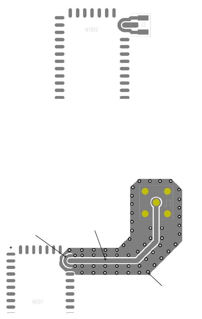
Bluegiga Technologies Oy
Page 21 of 43
Figure 7: Layout of WT41-N with U.FL connector placed next to the RF pin
5.2.2 Layout for WT41-N with 50 ohm trace from RF pin to a SMA connector
Use 50 ohm transmission line to trace the signal from RF pin to an external RF connector. Figure 6 shows a
layout example for WT41-N with an external SMA connector.
GND stitching vias separated
by max 3 mm
50 ohm trace from RF pin
to a SMA connector
GND contact
for the RF pin
Figure 8: Example RF trace for WT41-N
A transmission line impedance calculator, such as TX-Line made by AWR, can be used to approximate the
dimensions for the 50 ohm transmission line. Figure 7 shows an example for two different 50 ohm
transmission lines.
Bluegiga Technologies Oy
Page 22 of 43
FR4, εr= 4.6
Prepreg, εr= 3.7
W = 0.15 mm
h = 0.076 mm
G = 0.25 mm
GND stitching vias
RF GROUND
RF GROUND RF GROUND
RF GROUND
FR4, εr= 4.6
h = 1 mm
W = 1.8 mm
MICROSTRIP
CPW Ground
Figure 9: Example cross section of two different 50 ohm transmission line
Bluegiga Technologies Oy
Page 23 of 43
6 UART Interface
This is a standard UART interface for communicating with other serial devices.WT41 UART interface provides
a simple mechanism for communicating with other serial devices using the RS232 protocol.
Four signals are used to implement the UART function. When WT41 is connected to another digital device,
UART_RX and UART_TX transfer data between the two devices. The remaining two signals, UART_CTS and
UART_RTS, can be used to implement RS232 hardware flow control where both are active low indicators. All
UART connections are implemented using CMOS technology and have signalling levels of 0V and VDD.
UART configuration parameters, such as data rate and packet format, are set using WT41 software.
Note:
In order to communicate with the UART at its maximum data rate using a standard PC, an accelerated serial
port adapter card is required for the PC.
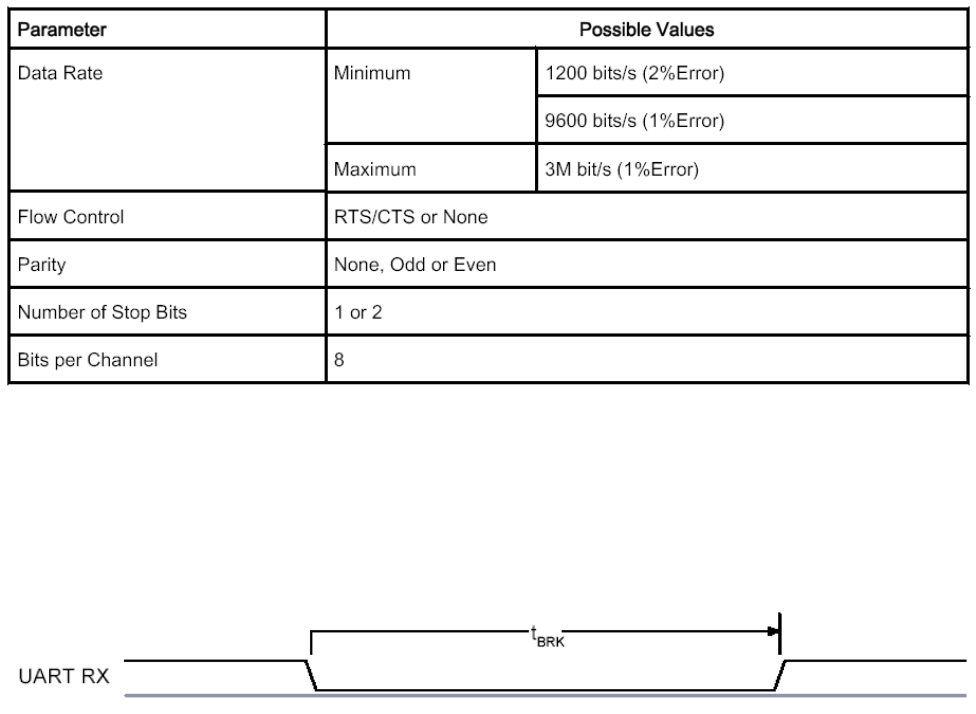
Table 16: Possible UART Settings
The UART interface is capable of resetting WT41 upon reception of a break signal. A break is identified by a
continuous logic low (0V) on the UART_RX terminal, as shown in Figure XXX. If tBRK is longer than the
value, defined by PSKEY_HOST_IO_UART_RESET_TIMEOUT, (0x1a4), a reset will occur. This feature
allows a host to initialise the system to a known state. Also, WT41 can emit a break character that may be
used to wake the host.
Figure 10: Break Signal
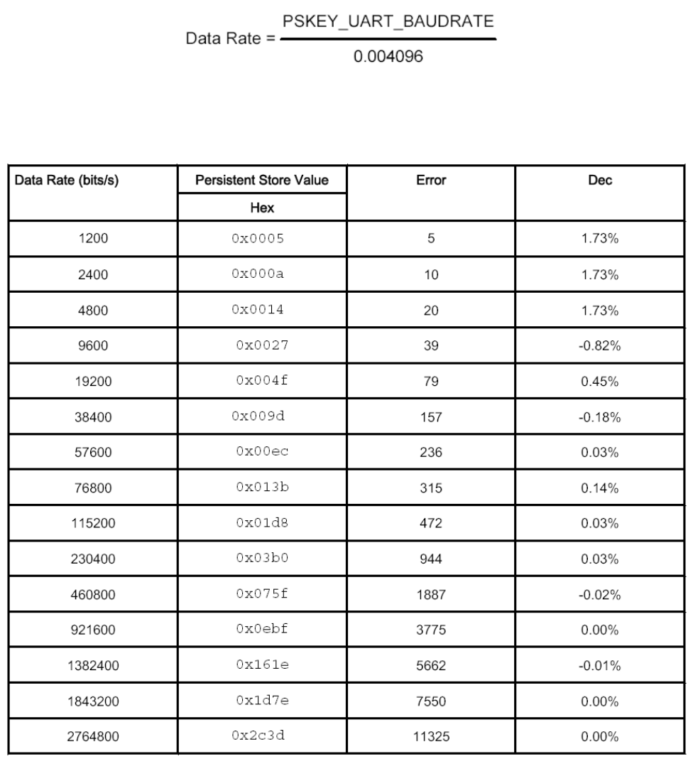
Table XXX shows a list of commonly used data rates and their associated values for
PSKEY_UART_BAUD_RATE (0x204). There is no requirement to use these standard values. Any data rate
within the supported range can be set in the PS Key according to the formula in Equation XXX
Bluegiga Technologies Oy
Page 24 of 43
Equation 1: Data Rate
Table 17: Standard Data Rates
Bluegiga Technologies Oy
Page 25 of 43
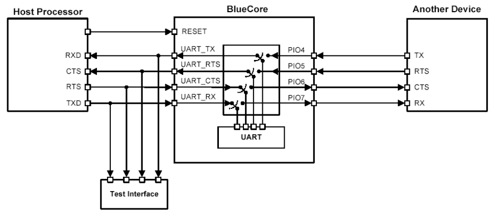
6.1 UART Bypass
Figure 11: UART Bypass Architecture
6.2 UART Configuration While Reset is Active
The UART interface for WT41 while the chip is being held in reset is tristate. This will allow the user to daisy
chain devices onto the physical UART bus. The constraint on this method is that any devices connected to
this bus must tristate when WT41 reset is de-asserted and the firmware begins to run.
6.3 UART Bypass Mode
Alternatively, for devices that do not tristate the UART bus, the UART bypass mode on BlueCore4-External
can be used. The default state of BlueCore4-External after reset is de-asserted; this is for the host UART bus
to be connected to the BlueCore4-External UART, thereby allowing communication to BlueCore4-External via
the UART. All UART bypass mode connections are implemented using CMOS technology and have signalling
levels of 0V and VDD.
In order to apply the UART bypass mode, a BCCMD command will be issued to BlueCore4-External. Upon
this issue, it will switch the bypass to PIO[7:4] as Figure XXX indicates. Once the bypass mode has been
invoked, WT41 will enter the Deep Sleep state indefinitely.
In order to re-establish communication with WT41, the chip must be reset so that the default configuration
takes effect.
It is important for the host to ensure a clean Bluetooth disconnection of any active links before the bypass
mode is invoked. Therefore, it is not possible to have active Bluetooth links while operating the bypass mode.
The current consumption for a device in UART bypass mode is equal to the values quoted for a device in
standby mode.
Bluegiga Technologies Oy
Page 26 of 43
7 USB Interface
This is a full speed (12Mbits/s) USB interface for communicating with other compatible digital devices. WT41
acts as a USB peripheral, responding to requests from a master host controller such as a PC.
The USB interface is capable of driving a USB cable directly. No external USB transceiver is required. The
device operates as a USB peripheral, responding to requests from a master host controller such as a PC.
Both the OHCI and the UHCI standards are supported. The set of USB endpoints implemented can behave as
specified in the USB section of the Bluetooth v2.1 + EDR specification or alternatively can appear as a set of
endpoints appropriate to USB audio devices such as speakers.
As USB is a master/slave oriented system (in common with other USB peripherals), WT41 only supports USB
Slave operation.
7.1 USB Data Connections
The USB data lines emerge as pins USB_DP and USB_DN. These terminals are connected to the internal
USB I/O buffers of the BlueCore4-External, therefore, have a low output impedance. To match the connection
to the characteristic impedance of the USB cable, resistors must be placed in series with USB_DP/USB_DN
and the cable.
7.2 USB Pull-Up resistor
WT41 features an internal USB pull-up resistor. This pulls the USB_DP pin weakly high when WT41 is ready
to enumerate. It signals to the PC that it is a full speed (12Mbits/s) USB device.
The USB internal pull-up is implemented as a current source, and is compliant with section 7.1.5 of the USB
specification v1.2. The internal pull-up pulls USB_DP high to at least 2.8V when loaded with a 15k 5% pull-
down resistor (in the hub/host) when VDD_PADS = 3.1V. This presents a Thevenin resistance to the host of
at least 900. Alternatively, an external 1.5k pull-up resistor can be placed between a PIO line and D+ on the
USB cable. The firmware must be alerted to which mode is used by setting PSKEY_USB_PIO_PULLUP
appropriately. The default setting uses the internal pull-up resistor.
7.3 USB Power Supply
The USB specification dictates that the minimum output high voltage for USB data lines is 2.8V. To safely
meet the USB specification, the voltage on the VDD supply terminal must be an absolute minimum of 3.1V.
Bluegiga recommends 3.3V for optimal USB signal quality.
7.4 Self-Powered Mode
In self-powered mode, the circuit is powered from its own power supply and not from the VBUS (5V) line of the
USB cable. It draws only a small leakage current (below 0.5mA) from VBUS on the USB cable. This is the
easier mode for which to design, as the design is not limited by the power that can be drawn from the USB
hub or root port. However, it requires that VBUS be connected to WT41 via a resistor network (Rvb1 and
Rvb2), so WT41 can detect when VBUS is powered up. BlueCore4-External will not pull USB_DP high when
VBUS is off.
Self-powered USB designs (powered from a battery or PSU) must ensure that a PIO line is allocated for USB
pullup purposes. A 1.5k 5% pull-up resistor between USB_DP and the selected PIO line should be fitted to the
design. Failure to fit this resistor may result in the design failing to be USB compliant in self-powered mode.
The internal pull-up in BlueCore is only suitable for bus-powered USB devices, e.g., dongles.
Bluegiga Technologies Oy
Page 27 of 43
Figure 12: USB Connections for Self-Powered Mode
The terminal marked USB_ON can be any free PIO pin. The PIO pin selected must be registered by setting
PSKEY_USB_PIO_VBUS to the corresponding pin number.
Figure 13: USB Interface Component Values
7.5 Bus-Powered Mode
In bus-powered mode, the application circuit draws its current from the 5V VBUS supply on the USB cable.
WT41 negotiates with the PC during the USB enumeration stage about how much current it is allowed to
consume. On power-up the device must not draw more than 100 mA but after being configured it can draw up
to 500 mA.
For WT41, the USB power descriptor should be altered to reflect the amount of power required. This is
accomplished by setting PSKEY_USB_MAX_POWER (0x2c6). This is higher than for a Class 2 application
due to the extra current drawn by the Transmit RF PA. By default for WT41 the setting is 300 mA.
When selecting a regulator, be aware that VBUS may go as low as 4.4V. The inrush current (when charging
reservoir and supply decoupling capacitors) is limited by the USB specification. See the USB Specification.
Some applications may require soft start circuitry to limit inrush current if more than 10uF is present between
VBUS and GND. The 5V VBUS line emerging from a PC is often electrically noisy. As well as regulation down
to 3.3V and 1.8V, applications should include careful filtering of the 5V line to attenuate noise that is above the
voltage regulator bandwidth. Excessive noise on WT41 supply pins will result in reduced receiver sensitivity
and a distorted RF transmit signal.
Bluegiga Technologies Oy
Page 28 of 43
Figure 14: USB Connections for Bus-Powered Mode
7.6 USB Suspend Current
All USB devices must permit the USB controller to place them in a USB suspend mode. While in USB
Suspend, bus-powered devices must not draw more than 2.5mA from USB VBUS (self-powered devices may
draw more than 2.5mA from their own supply). This current draw requirement prevents operation of the radio
by bus-powered devices during USB Suspend.
When computing suspend current, the current from VBUS through the bus pull-up and pull-down resistors
must be included. The pull-up resistor at the device is 1.5 k. (nominal). The pull-down resistor at the hub is
14.25k. to 24.80k. The pull-up voltage is nominally 3.3V, which means that holding one of the signal lines high
takes approximately 200uA, leaving only 2.3mA available from a 2.5mA budget. Ensure that external LEDs
and/or amplifiers can be turned off by BlueCore4-External. The entire circuit must be able to enter the
suspend mode.
7.7 USB Detach and Wake-Up Signaling
WT41 can provide out-of-band signaling to a host controller by using the control lines called USB_DETACH
and USB_WAKE_UP. These are outside the USB specification (no wires exist for them inside the USB cable),
but can be useful when embedding WT41 into a circuit where no external USB is visible to the user. Both
control lines are shared with PIO pins and can be assigned to any PIO pin by setting
PSKEY_USB_PIO_DETACH and PSKEY_USB_PIO_WAKEUP to the selected PIO number.
USB_DETACH is an input which, when asserted high, causes WT41 to put USB_DN and USB_DP in high
impedance state and turns off the pull-up resistor on DP. This detaches the device from the bus and is
logically equivalent to unplugging the device. When USB_DETACH is taken low, WT41 will connect back to
USB and await enumeration by the USB host.
USB_WAKE_UP is an active high output (used only when USB_DETACH is active) to wake up the host and
allow USB communication to recommence. It replaces the function of the software USB WAKE_UP message
(which runs over the USB cable) and cannot be sent while BlueCore4-External is effectively disconnected
from the bus.
Bluegiga Technologies Oy
Page 29 of 43
Figure 15: USB_Detach and USB_Wake_Up Signals
7.8 USB Driver
A USB Bluetooth device driver is required to provide a software interface between BlueCore4-External and
Bluetooth software running on the host computer. Please, contact support@bluegiga.com for suitable drivers.
7.9 USB v2.0 Compliance and Compatibility
Although WT41 meets the USB specification, CSR cannot guarantee that an application circuit designed
around the module is USB compliant. The choice of application circuit, component choice and PCB layout all
affect USB signal quality and electrical characteristics. The information in this document is intended as a guide
and should be read in association with the USB specification, with particular attention being given to Chapter
7. Independent USB qualification must be sought before an application is deemed USB compliant and can
bear the USB logo. Such qualification can be obtained from a USB plugfest or from an independent USB test
house.
Terminals USB_DP and USB_DN adhere to the USB Specification v2.0 (Chapter 7) electrical requirements.
BlueCore4-External is compatible with USB v2.0 host controllers; under these circumstances the two ends
agree the mutually acceptable rate of 12Mbits/s according to the USB v2.0 specification.

Bluegiga Technologies Oy
Page 30 of 43
8 Serial Peripheral Interface (SPI)
The SPI port can be used for system debugging. It can also be used for programming the Flash memory and
setting the PSKEY configurations. WT41 uses 16-bit data and 16-bit address serial peripheral interface, where
transactions may occur when the internal processor is running or is stopped. SPI interface is connected using
the MOSI, MISO, CSB and CLK pins. Please, contact support@bluegiga.com for detailed information about
the instruction cycle.
Bluegiga Technologies Oy
Page 31 of 43
9 PCM Codec Interface
PCM is a standard method used to digitize audio (particularly voice) for transmission over digital
communication channels. Through its PCM interface, WT41 has hardware support for continual transmission
and reception of PCM data, thus reducing processor overhead for wireless headset applications. WT41 offers
a bidirectional digital audio interface that routes directly into the baseband layer of the on-chip firmware. It
does not pass through the HCI protocol layer.
Hardware on WT41 allows the data to be sent to and received from a SCO connection. Up to three SCO
connections can be supported by the PCM interface at any one time.
WT41 can operate as the PCM interface master generating an output clock of 128, 256 or 512kHz. When
configured as PCM interface slave, it can operate with an input clock up to 2048kHz. WT41 is compatible with
a variety of clock formats, including Long Frame Sync, Short Frame Sync and GCI timing environments.
It supports 13-bit or 16-bit linear, 8-bit µ-law or A-law companded sample formats at 8ksamples/s and can
receive and transmit on any selection of three of the first four slots following PCM_SYNC. The PCM
configuration options are enabled by setting PSKEY_PCM_CONFIG32.
WT41 interfaces directly to PCM audio devices.
NOTE: Analog audio lines are very sensitive to RF disturbance. Use good layout practices to ensure noise
less audio. Make sure that the return path for the audio signals follows the forward current all the way as close
as possible and use fully differential signals when possible. Do not compromise audio routing.
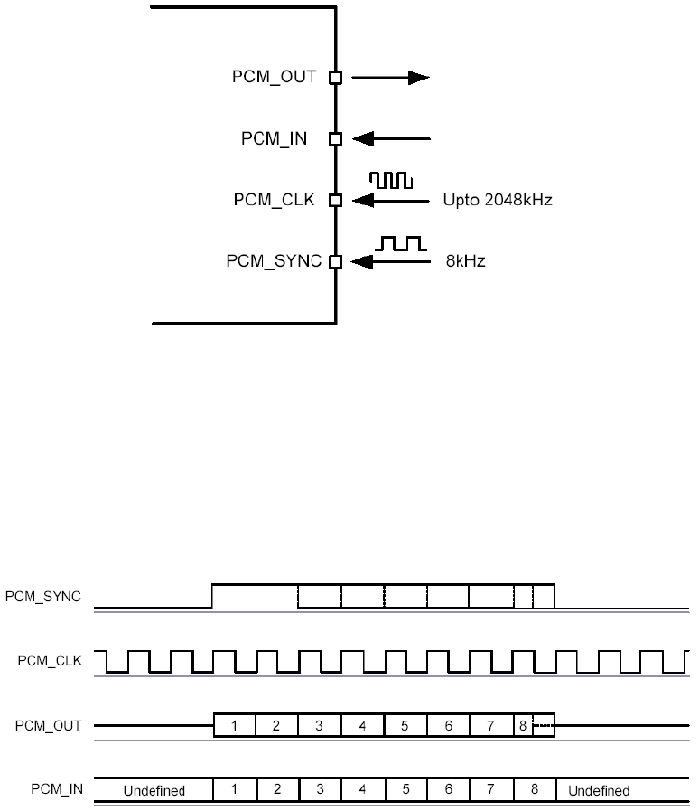
9.1 PCM Interface Master/Slave
When configured as the master of the PCM interface, WT41 generates PCM_CLK and PCM_SYNC.
Figure 16: PCM Interface Master
When configured as the Slave of the PCM interface, WT41 accepts PCM_CLK rates up to 2048kHz.
Bluegiga Technologies Oy
Page 32 of 43
Figure 17: PCM Interface Slave
9.2 Long Frame Sync
Long Frame Sync is the name given to a clocking format that controls the transfer of PCM data words or
samples. In Long Frame Sync, the rising edge of PCM_SYNC indicates the start of the PCM word. When
WT41 is configured as PCM master, generating PCM_SYNC and PCM_CLK, then PCM_SYNC is 8-bits long.
When WT41 is configured as PCM Slave, PCM_SYNC may be from two consecutive falling edges of
PCM_CLK to half the PCM_SYNC rate, i.e., 62.5s long.
Figure 18: Long Frame Sync (Shown with 8-bit Companded Sample)
WT41 samples PCM_IN on the falling edge of PCM_CLK and transmits PCM_OUT on the rising edge.
PCM_OUT may be configured to be high impedance on the falling edge of PCM_CLK in the LSB position or
on the rising edge.
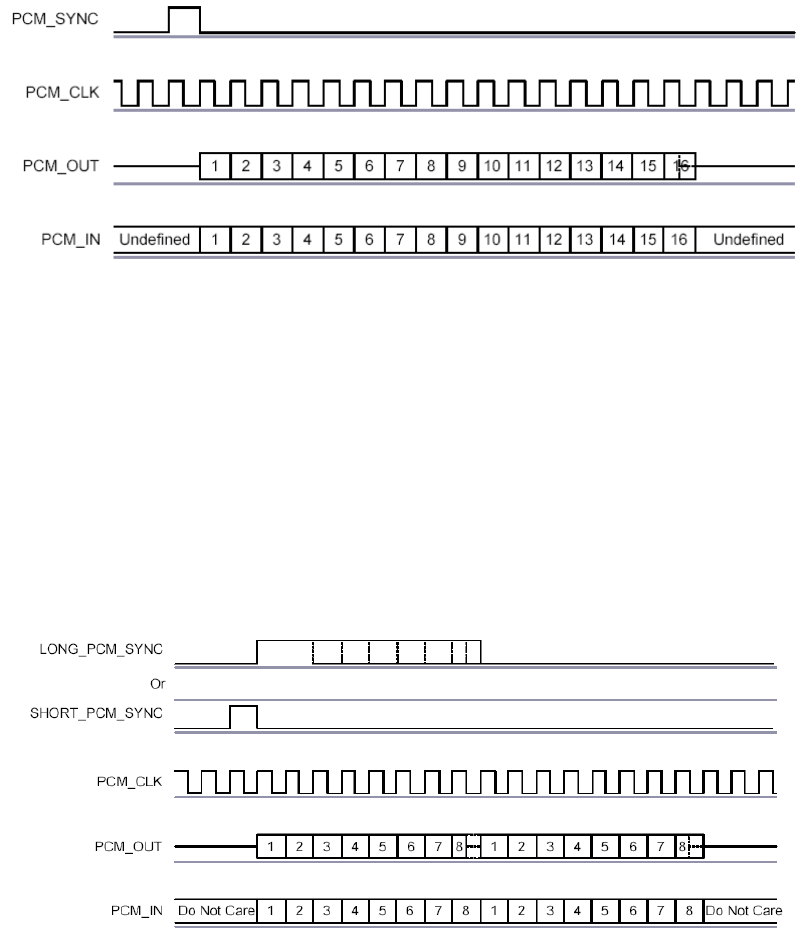
9.3 Short Frame Sync
In Short Frame Sync, the falling edge of PCM_SYNC indicates the start of the PCM word. PCM_SYNC is
always one clock cycle long.
Bluegiga Technologies Oy
Page 33 of 43
Figure 19: Short Frame Sync (Shown with 16-bit Sample)
As with Long Frame Sync, WT41 samples PCM_IN on the falling edge of PCM_CLK and transmits PCM_OUT
on the rising edge. PCM_OUT may be configured to be high impedance on the falling edge of PCM_CLK in
the LSB position or on the rising edge.
9.4 Multi-slot Operation
More than one SCO connection over the PCM interface is supported using multiple slots. Up to three SCO
connections can be carried over any of the first four slots.
Figure 20: Multi-slot Operation with Two Slots and 8-bit Companded Samples
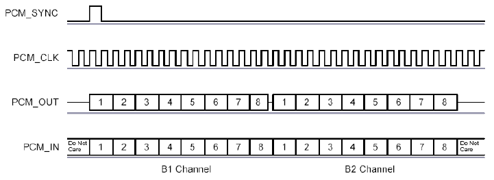
9.5 GCI Interface
WT41 is compatible with the GCI, a standard synchronous 2B+D ISDN timing interface. The two 64kbits/s B
channels can be accessed when this mode is configured.
Bluegiga Technologies Oy
Page 34 of 43
Figure 21: GCI Interface
The start of frame is indicated by the rising edge of PCM_SYNC and runs at 8kHz. With WT41 in Slave mode,
the frequency of PCM_CLK can be up to 4.096MHz.
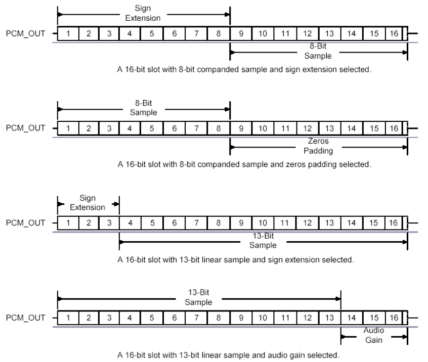
9.6 Slots and Sample Formats
WT41 can receive and transmit on any selection of the first four slots following each sync pulse. Slot durations
can be either 8 or 16 clock cycles. Durations of 8 clock cycles may only be used with 8-bit sample formats.
Durations of 16 clocks may be used with 8-bit, 13-bit or 16-bit sample formats.
WT41 supports 13-bit linear, 16-bit linear and 8-bit -law or A-law sample formats. The sample rate is
8ksamples/s. The bit order may be little or big endian. When 16-bit slots are used, the 3 or 8 unused bits in
each slot may be filled with sign extension, padded with zeros or a programmable 3-bit audio attenuation
compatible with some Motorola codecs.
Bluegiga Technologies Oy
Page 35 of 43
Figure 22: 16-bit Slot Length and Sample Formats
9.7 Additional Features
WT41 has a mute facility that forces PCM_OUT to be 0. In master mode, PCM_SYNC may also be forced to 0
while keeping PCM_CLK running which some codecs use to control power down.
9.8 PCM_CLK and PCM_SYNC Generation
WT41 has two methods of generating PCM_CLK and PCM_SYNC in master mode. The first is generating
these signals by DDS from BlueCore4-External internal 4MHz clock. Using this mode limits PCM_CLK to 128,
256 or 512kHz and PCM_SYNC to 8kHz. The second is generating PCM_CLK and PCM_SYNC by DDS from
an internal 48MHz clock (which allows a greater range of frequencies to be generated with low jitter but
consumes more power). This second method is selected by setting bit 48M_PCM_CLK_GEN_EN in
PSKEY_PCM_CONFIG32. When in this mode and with long frame sync, the length of PCM_SYNC can be
either 8 or 16 cycles of PCM_CLK, determined by LONG_LENGTH_SYNC_EN in PSKEY_PCM_CONFIG32.
The Equation XXX describes PCM_CLK frequency when being generated using the internal 48MHz clock:
Bluegiga Technologies Oy
Page 36 of 43
Equation 2: PCM_CLK Frequency When Being Generated Using the Internal 48MHz Clock
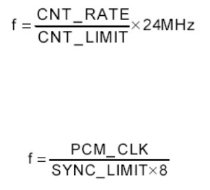
The frequency of PCM_SYNC relative to PCM_CLK can be set using Equation XXX:
Equation 3: PCM_SYNC Frequency Relative to PCM_CLK
CNT_RATE, CNT_LIMIT and SYNC_LIMIT are set using PSKEY_PCM_LOW_JITTER_CONFIG. As an
example, to generate PCM_CLK at 512kHz with PCM_SYNC at 8kHz, set
PSKEY_PCM_LOW_JITTER_CONFIG to 0x08080177.
9.9 PCM Configuration
The PCM configuration is set using two PS Keys, PSKEY_PCM_CONFIG32 detailed in Table XXX and
PSKEY_PCM_LOW_JITTER_CONFIG in Table XXX. The default for PSKEY_PCM_CONFIG32 is
0x00800000, i.e., first slot following sync is active, 13-bit linear voice format, long frame sync and interface
master generating 256kHz PCM_CLK from 4MHz internal clock with no tri-state of PCM_OUT.

Bluegiga Technologies Oy
Page 37 of 43
Name Bit position Description
-0Set to 0
SLAVE MODE EN 1
0 selects Master mode with internal generation of PCM_CLK and
PCM_SYNC. 1 selects Slave mode requiring externally generated
PCM_CLK and PCM_SYNC. This should be set to 1 if
48M_PCM_CLK_GEN_EN (bit 11) is set.
SHORT SYNC EN 20 selects long frame sync (rising edge indicates start of frame), 1
selects short frame sync (falling edge indicates start of frame).
- 3 Set to 0
SIGN EXTENDED
EN 4
0 selects padding of 8 or 13-bit voice sample into a 16- bit slot by
inserting extra LSBs, 1 selects sign extension. When padding is
selected with 3-bit voice sample, the 3 padding bits are the audio gain
setting; with 8-bit samples the 8 padding bits are zeroes.
LSB FIRST EN 50 transmits and receives voice samples MSB first, 1 uses LSB first.
TX TRISTATE EN 6
0 drives PCM_OUT continuously, 1 tri-states PCM_OUT immediately
after the falling edge of PCM_CLK in the last bit of an active slot,
assuming the next slot is not active.
TX TRISTATE
RISING EDGE EN 7
0 tristates PCM_OUT immediately after the falling edge of PCM_CLK
in the last bit of an active slot, assuming the next slot is also not active.
1 tristates PCM_OUT after the rising edge of PCM_CLK.
SYNC SUPPRESS
EN 8
0 enables PCM_SYNC output when master, 1 suppresses PCM_SYNC
whilst keeping PCM_CLK running. Some CODECS utilize this to enter
a low power state.
GCI MODE EN 91 enables GCI mode.
MUTE EN 10 1 forces PCM_OUT to 0.
48M PCM CLK GEN
EN 11
0 sets PCM_CLK and PCM_SYNC generation via DDS from internal 4
MHz clock, as for BlueCore4-External. 1 sets PCM_CLK and
PCM_SYNC generation via DDS from internal 48 MHz clock.
LONG LENGTH
SYNC EN 12
0 sets PCM_SYNC length to 8 PCM_CLK cycles and 1 sets length to
16 PCM_CLK cycles. Only applies for long frame sync and with
48M_PCM_CLK_GEN_EN set to 1.
-[20:16] Set to 0b00000.
MASTER CLK RATE [22:21] Selects 128 (0b01), 256 (0b00), 512 (0b10) kHz PCM_CLK frequency
when master and 48M_PCM_CLK_GEN_EN (bit 11) is low.
ACTIVE SLOT [26:23] Default is 0001. Ignored by firmaware
SAMPLE_FORMAT [28:27]
Selects between 13 (0b00), 16 (0b01), 8 (0b10) bit sample with 16
cycle slot duration 8 (0b11) bit sample 8 cycle slot duration.
Table 18: PSKEY_PCM_CONFIG32 description
Name Bit position Description
CNT LIMIT [12:0] Sets PCM_CLK counter limit
CNT RATE [23:16] Sets PCM_CLK count rate.
SYNC LIMIT [31:24] Sets PCM_SYNC division relative to PCM_CLK.
Table 19: PSKEY_PCM_LOW_JITTER_CONFIG Description
Bluegiga Technologies Oy
Page 38 of 43
10 I/O Parallel Ports
Six lines of programmable bidirectional input/outputs (I/O) are provided. All the PIO lines are power from VDD.
PIO lines can be configured through software to have either weak or strong pull-ups or pull-downs. All PIO
lines are configured as inputs with weak pull-downs at reset. Any of the PIO lines can be configured as
interrupt request lines or as wake-up lines from sleep modes.
WT41 has a general purpose analogue interface pin AIO[1]. This is used to access internal circuitry and
control signals. It may be configured to provide additional functionality.
Auxiliary functions available via AIO[1] include an 8-bit ADC and an 8-bit DAC. Typically the ADC is used for
battery voltage measurement. Signals selectable at this pin include the band gap reference voltage and a
variety of clock signals: 48, 24, 16, 8MHz and the XTAL clock frequency. When used with analogue signals,
the voltage range is constrained by the analogue supply voltage internally to the module (1.8V). When
configured to drive out digital level signals (e.g., clocks), the output voltage level is determined by VDD.
10.1 PIO Defaults
Bluegiga cannot guarantee that these terminal functions remain the same. Refer to the software release note
for the implementation of these PIO lines, as they are firmware build-specific.
Bluegiga Technologies Oy
Page 39 of 43
11 Reset
WT41 may be reset from several sources: RESET pin, power on reset, a UART break character or via
software configured watchdog timer. The RESET pin is an active low reset and is internally filtered using the
internal low frequency clock oscillator. A reset will be performed between 1.5 and 4.0ms following RESETB
being active. It is recommended that RESET be applied for a period greater than 5ms.
The power on reset occurs when the VDD_CORE supply internally to the module falls below typically 1.5V
and is released when VDD_CORE rises above typically 1.6V. At reset the digital I/O pins are set to inputs for
bidirectional pins and outputs are tri-state.
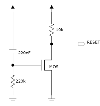
The reset should be held active at power up until all the supply voltages have stabilized to ensure correct
operation of the internal flash memory. Following figure shows an example of a simple power up reset circuit.
Time constant of the RC circuitry is set so that the supply voltage is safely stabilized before the reset
deactivates.
Figure 23: Example of a simple power on reset circuit.

Bluegiga Technologies Oy
Page 40 of 43
11.1 Pin States on Reset
PIN NAME STATE
PIO[7:2] Input with weak pull-down
PCM_OUT Tri-staed with weak pull-down
PCM_IN Input with weak pull-down
PCM_SYNC Input with weak pull-down
PCM_CLK Input with weak pull-down
UART_TX Output tristated with weak pull-up
UART_RX Input with weak pull-down
UART_RTS Output tristated with weak pull-up
UART_CTS Input with weak pull-down
USB+ Input with weak pull-down
USB- Input with weak pull-down
SPI_CSB Input with weak pull-down
SPI_CLK Input with weak pull-down
SPI_MOSI Input with weak pull-down
SPI_MISO Output tristated with weak pull-down
AIO[1] Output, driving low
Table 20: Pin States on Reset

Bluegiga Technologies Oy
Page 41 of 43
12 Certifications
WT41 is compliant to the following specifications.
12.1 Bluetooth
WT41 module is Bluetooth qualified and listed as a controller subsystem and it is Bluetooth compliant to the
following profiles of the core spec version 2.1/2.1+EDR.
TBA
12.2 FCC
This device complies with Part 15 of the FCC Rules. Operation is subject to the following two conditions:
(1) this device may not cause harmful interference, and
(2) this device must accept any interference received, including interference that may
cause undesired operation.
FCC RF Radiation Exposure Statement:
This equipment complies with FCC radiation exposure limits set forth for an uncontrolled environment. End
users must follow the specific operating instructions for satisfying RF exposure compliance. This transmitter
must not be co-located or operating in conjunction with any other antenna or transmitter. This transmitter is
considered as mobile device and should not be used closer than 20 cm from a human body. To allow portable
use in a known host class 2 permissive change is required. Please contact support@bluegiga.com for detailed
information.
Note:
When using WT41-A or WT41-N the end product must display an exterior label with the following detail
incorporated: “Contains Transmitter Module FCC ID: QOQWT41”
Bluegiga Technologies Oy
Page 42 of 43
12.3 CE
WT41 meets the requirements of the standards below and hence fulfills the requirements of EMC Directive
89/336/EEC as amended by Directives 92/31/EEC and 93/68/EEC within CE marking requirement.
• EMC (immunity only) EN 301 489-17 V.1.3.3 in accordance with EN 301 489-1 V1.8.1
• Radiated emissions EN 300 328 V1.7.1
12.4 Industry Canada (IC)
WT41 meets Industry Canada’s procedural and specification requirements for certification.
Industry Canada ID: 5123A-BGTWT41
12.5 Japan
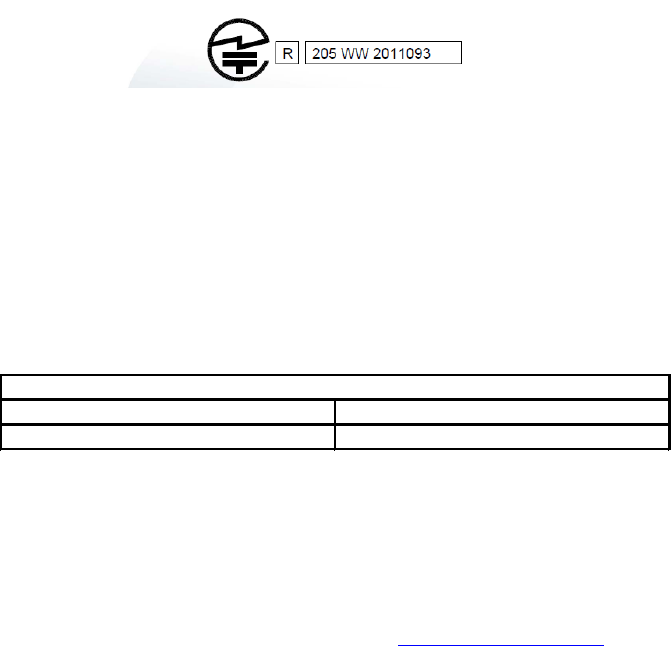
WT41-A is certified for Japanese market with certification number 2011093/01. The rated transmit power is
1mW/MHz without AFH (adaptive frequency hopping). Japan’s regulations limit the maximum spectral power
density to 3mW/MHz. When using AFH the number of active channels can be as low as 20 which will
effectively increase the spectral power density. Thus when AFH is in use the transmit power must be
decreased nominally to 13 dBm to meet Japan regulations.
Figure 24: Identification code for Japanese market
12.6 Qualified Antenna Types for WT41-N
This device has been designed to operate with the antennas listed below, and having a maximum gain of 2
dB. Antennas not included in this list or having a gain greater than 2 dB are strictly prohibited for use with this
device. The required antenna impedance is 50 ohms.
Antenna Type Maximum Gain
Dipole 2.3 dBi
Qualified Antenna Types for WT41-N
Table 21: Qualified Antenna Types for WT41-N
Any antenna that is of the same type and of equal or less directional gain as listed in table 14 can be used
without a need for retesting. To reduce potential radio interference to other users, the antenna type and its
gain should be so chosen that the equivalent isotropically radiated power (e.i.r.p.) is not more than that
permitted for successful communication. Using an antenna of a different type or gain more than 2.2 dBi will
require additional testing for FCC, CE and IC. Please, contact support@bluegiga.com for more information.

Bluegiga Technologies Oy
Page 43 of 43
13 Contact Information
Sales: sales@bluegiga.com
Technical support: support@bluegiga.com
http://www.bluegiga.com/techforum/
Orders: orders@bluegiga.com
Head Office / Finland:
Phone: +358-9-4355 060
Fax: +358-9-4355 0660
Street Address:
Sinikalliontie 5A
02630 ESPOO
FINLAND
Postal address:
P.O. BOX 120
02631 ESPOO
FINLAND
Sales Office / USA:
Phone: (781) 556-1039
Bluegiga Technologies, Inc.
99 Derby Street, Suite 200 Hingham, MA 02043