Simcom 1005242010007 SIM900B Wireless Module User Manual
Shanghai Simcom Ltd. SIM900B Wireless Module
UserManual.wiki
>
Simcom
>
1005242010007 User Manual
>
User Manual
Contents
1.
Mounting Information
2.
User Manual
3.
Users Manual
User Manual
Navigation menu
Upload a User Manual
Namespaces
Wiki Guide
HTML
PDF
Info
Views
User Manual
Discussion / Help
Navigation

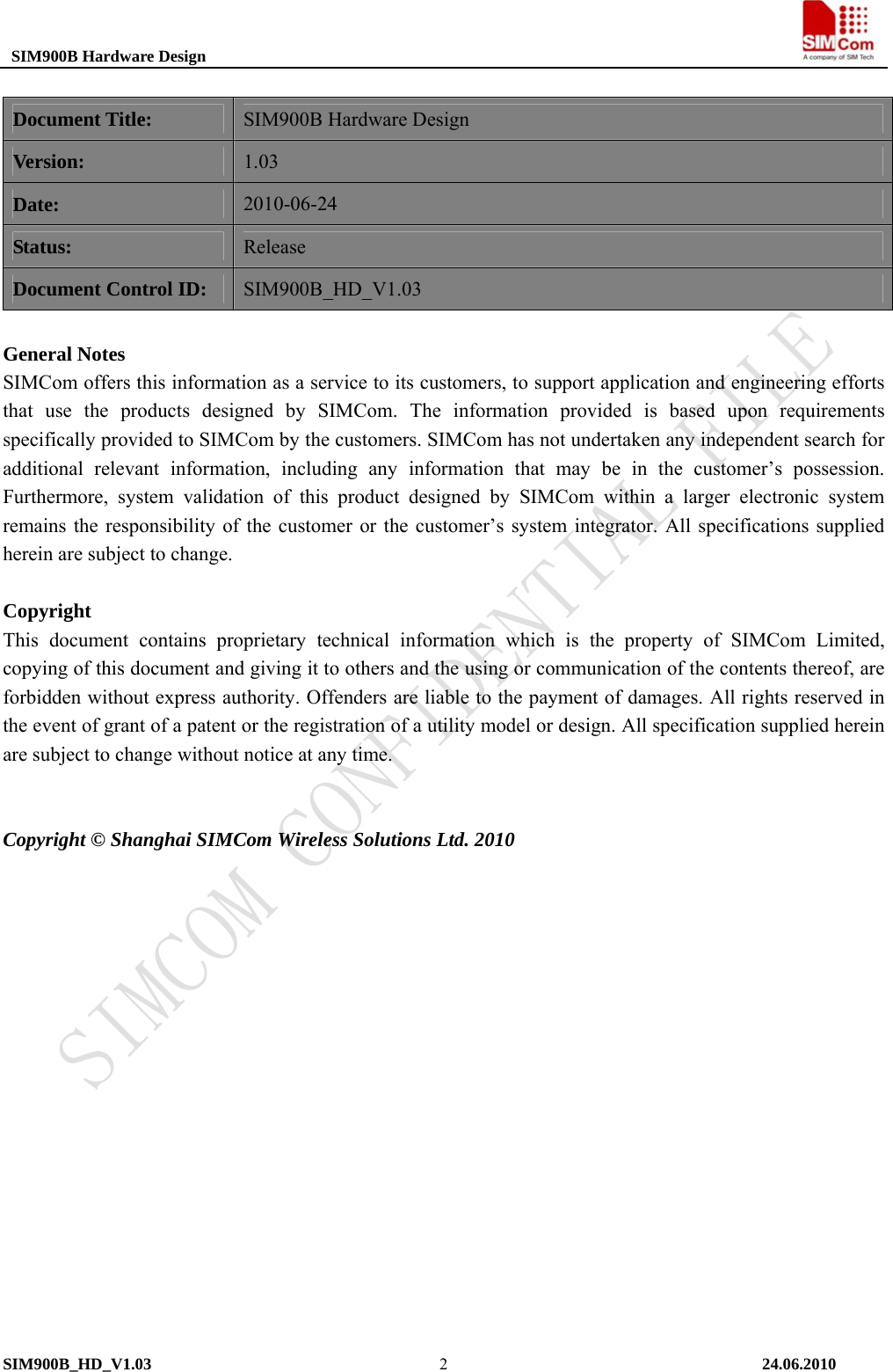
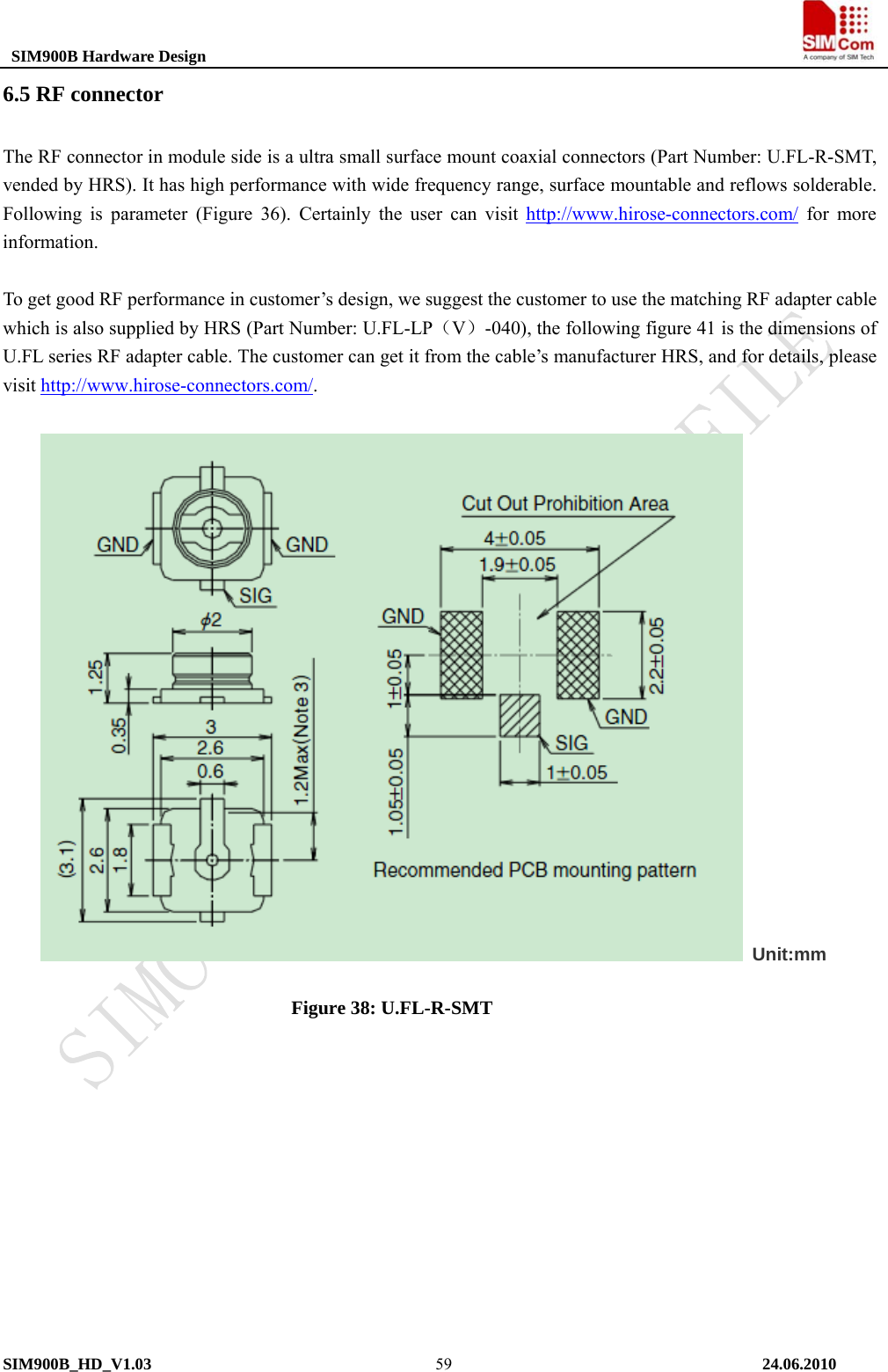
![SIM900B Hardware Design 1 Introduction This document describes the hardware interface of the SIMCom SIM900B module that connects to the specific application and the air interface. As SIM900B can be integrated with a wide range of applications, all functional components of SIM900B are described in great detail. This document can help you quickly understand SIM900B interface specifications, electrical and mechanical details. With the help of this document and other SIM900B application notes, user guide, the user can use SIM900B module to design and set-up mobile applications quickly. 1.1 Related Documents Table 1: Related documents SN Document name Remark [1] SIM900_ATC SIM900_ATC [2] ITU-T Draft new recommendation V.25ter: Serial asynchronous automatic dialing and control [3] GSM 07.07: Digital cellular telecommunications (Phase 2+); AT command set for GSM Mobile Equipment (ME) [4] GSM 07.10: Support GSM 07.10 multiplexing protocol [5] GSM 07.05: Digital cellular telecommunications (Phase 2+); Use of Data Terminal Equipment – Data Circuit terminating Equipment (DTE – DCE) interface for Short Message Service (SMS) and Cell Broadcast Service (CBS) [6] GSM 11.14: Digital cellular telecommunications system (Phase 2+); Specification of the SIM Application Toolkit for the Subscriber Identity Module – Mobile Equipment (SIM – ME) interface [7] GSM 11.11: Digital cellular telecommunications system (Phase 2+); Specification of the Subscriber Identity Module – Mobile Equipment (SIM – ME) interface [8] GSM 03.38: Digital cellular telecommunications system (Phase 2+); Alphabets and language-specific information [9] GSM 11.10 Digital cellular telecommunications system (Phase 2); Mobile Station (MS) conformance specification; Part 1: Conformance specification [10] AN_Serial Port AN_Serial Port 1.2 Terms and Abbreviations Table 2: Terms and Abbreviations SIM900B_HD_V1.03 24.06.2010 8](https://usermanual.wiki/Simcom/1005242010007.User-Manual/User-Guide-1319262-Page-8.png)
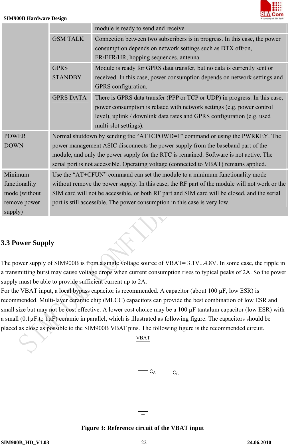
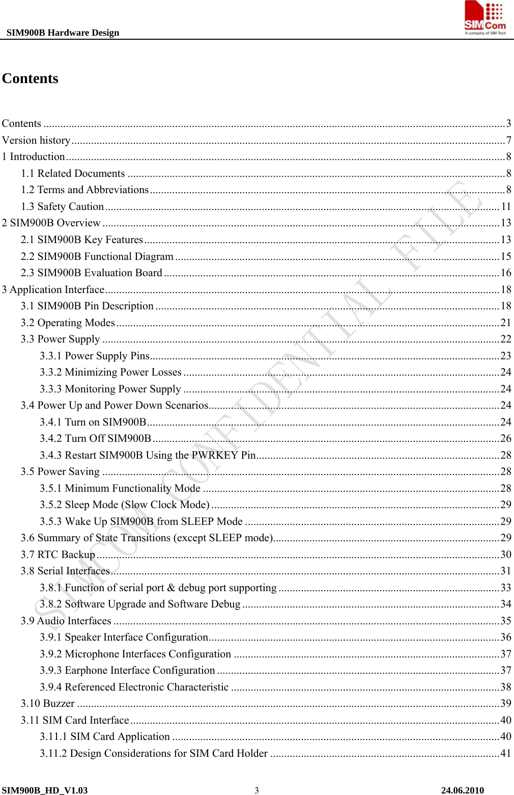
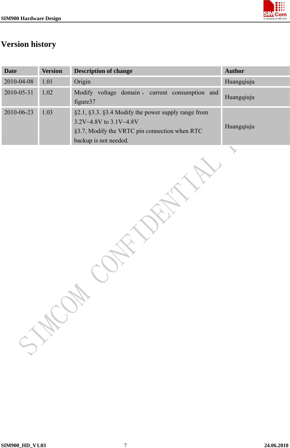
![SIM900B Hardware Design 3.3.2 Minimizing Power Losses When designing the power supply for your application please pay specific attention to power losses. Ensure that the input voltage VBAT never drops below 3.2V even in a transmit burst where current consumption can rise to typical peaks of 2A. If the power voltage drops below 3.2V, the module may be switched off. The PCB traces from the VBAT pins to the power source must be wide enough to decrease voltage drops in the transmitting burst mode. 3.3.3 Monitoring Power Supply To monitor the supply voltage, the user can use the “AT+CBC” command which include a parameter: voltage value (in mV). The voltage is continuously measured at intervals depending on the operating mode. The displayed voltage (in mV) is averaged over the last measuring period before the “AT+CBC” command is executed. For details please refer to document [1] 3.4 Power Up and Power Down Scenarios In general, be sure not to turn on SIM900B while it is beyond the safety limits of voltage and temperature stated in Chapter 3.4.2. SIM900B would immediately switch off after having started and detected these inappropriate conditions. In extreme cases this can cause permanent damage to the module. 3.4.1 Turn on SIM900B SIM900B can be turned on by the following way, which is described in following chapters: z Via PWRKEY pin: starts normal operating mode (please refer to chapter 3.4.1.1); Note: The AT command must be set after the SIM900B is power on and Unsolicited Result Code “RDY” is received from the serial port. However if the SIM900B is set autobauding, the serial port will receive nothing. The AT commands can be set after the SIM900B is power on. “AT+IPR=x” can be used to set a fixed baud rate and save the configuration to non-volatile flash memory. After the configuration is saved as fixed baud rate, the Code “RDY” should be received from the serial port all the time that the SIM900B is power on. Please refer to the chapter “AT+IPR” in document [1]. 3.4.1.1 Turn on SIM900B Using the PWRKEY Pin (Power on) The SIM900B can be turn on by driving the PWRKEY to a low level voltage for some time and then release. This pin has pulled up to a 3V voltage source in the module. The simple circuit illustrates as the following figures. SIM900B_HD_V1.03 24.06.2010 24](https://usermanual.wiki/Simcom/1005242010007.User-Manual/User-Guide-1319262-Page-24.png)
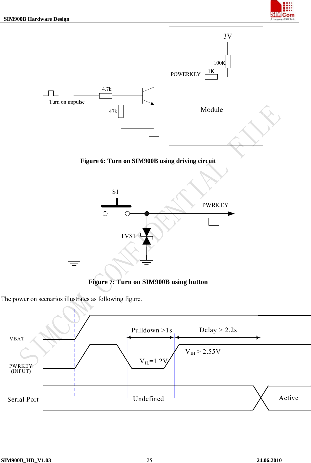
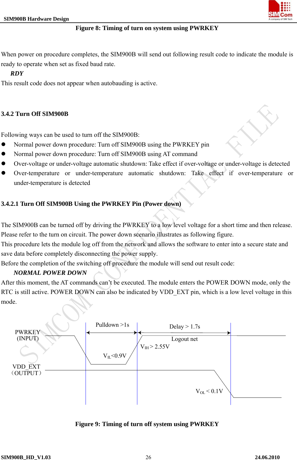
![SIM900B Hardware Design 3.4.2.2 Turn Off SIM900B Using AT Command AT command “AT+CPOWD=1”can be use to turn off the module. This command lets the module log off from the network and allows the module to enter into a secure state and save data before completely disconnecting the power supply. Before the completion of the switching off procedure the module will send out result code: NORMAL POWER DOWN After this moment, the AT commands can’t be executed. The module enters the POWER DOWN mode, only the RTC is still active. POWER DOWN can also be indicated by VDD_EXT pin, which is a low level voltage in this mode. Please refer to document [1] for detail about the AT command of “AT+CPOWD”. 3.4.2.3 Over-voltage or Under-voltage Automatic Shutdown The module will constantly monitor the voltage applied on the VBAT. If the voltage ≤ 3.2V, the following URC will be presented: UNDER-VOLTAGE WARNNING If the voltage ≥ 4.7V, the following URC will be presented: OVER-VOLTAGE WARNNING The uncritical voltage range is 3.1V to 4.8V. If the voltage > 4.8V or < 3.1V, the module will be automatic shutdown soon. If the voltage < 3.1V, the following URC will be presented: UNDER-VOLTAGE POWER DOWN If the voltage > 4.8V, the following URC will be presented: OVER-VOLTAGE POWER DOWN After this moment, no further more AT commands can be executed. The module logs off from network and enters POWER DOWN mode, and only the RTC is still active. POWER DOWN can also be indicated by VDD_EXT pin, which is a low level voltage in this mode. 3.4.2.4 Over-temperature or Under-temperature Automatic Shutdown The module will constantly monitor the temperature of the module, if the temperature > +80 , the following ℃URC will be presented: +CMTE:1 If the temperature < -30 , the following URC will be presented:℃ +CMTE:-1 The uncritical temperature range is -40 to ℃+85 . If the temperature ℃> +85 or ℃< -40 , the module will be ℃automatic shutdown soon. If the temperature >+ 85 , the following URC will be presented℃: +CMTE:2 If the temperature < -40℃, the following URC will be presented: +CMTE:-2 After this moment, the AT commands can’t be executed. The module logs off from network and enters POWER SIM900B_HD_V1.03 24.06.2010 27](https://usermanual.wiki/Simcom/1005242010007.User-Manual/User-Guide-1319262-Page-27.png)
![SIM900B Hardware Design DOWN mode, and only the RTC is still active. POWER DOWN can also be indicated by VDD_EXT pin, which is a low level voltage in this mode. To monitor the temperature, the “AT+CMTE” command can be used to read the temperature when the module is power on. For details please refer to document [1] 3.4.3 Restart SIM900B Using the PWRKEY Pin By driving the PWRKEY to a low level voltage for a short time and then release ,SIM900B can be restarted, the timing is the same as turning on SIM900B using the PWRKEY pin. Before restarting the SIM900B, you need delay at least 500ms from detecting the VDD_EXT low level on. The restarting scenario illustrates as the following figure. VDD_EXT(OUTPUT)HPWRKEY(INPUT)Delay > 500msTurn offPull down the PWRKEY to turn on the moduleRestart Figure 10: Timing of restart system 3.5 Power Saving There are two methods for the module to enter into low current consumption status. “AT+CFUN” is used to set module into minimum functionality mode and DTR signal can be used to control system enter or exit SLEEP mode (or slow clocking mode). 3.5.1 Minimum Functionality Mode Minimum functionality mode reduces the functionality of the module to a minimum and, thus, minimizes the current consumption to the lowest level. This mode is set with the “AT+CFUN” command which provides the choice of the functionality levels <fun>=0,1,4 z 0: minimum functionality; z 1: full functionality (default); z 4: disable phone both transmit and receive RF circuits; SIM900B_HD_V1.03 24.06.2010 28](https://usermanual.wiki/Simcom/1005242010007.User-Manual/User-Guide-1319262-Page-28.png)
![SIM900B Hardware Design If SIM900B has been set to minimum functionality by “AT+CFUN=0”, the RF function and SIM card function will be closed. In this case, the serial port is still accessible, but all AT commands correlative with RF function or SIM card function will not be accessible. If SIM900B has been set by “AT+CFUN=4”, the RF function will be closed, the serial port is still active. In this case all AT commands correlative with RF function will not be accessible. After SIM900B has been set by “AT+CFUN=0” or “AT+CFUN=4”, it can return to full functionality by “AT+CFUN=1”. For detailed information about “AT+CFUN”, please refer to document [1]. 3.5.2 Sleep Mode (Slow Clock Mode) DTR signal can be used to control SIM900B module to enter or exit the SLEEP mode in customer applications When DTR is in high level and there is no on air and hardware interrupt (such as GPIO interrupt or data on serial port), SIM900B will enter SLEEP mode automatically. In this mode, SIM900B can still receive paging or SMS from network but the serial port is not accessible. Note: For SIM900B, it requests to set AT command “AT+CSCLK=1” to enable the sleep mode; the default value is 0, that can’t make the module enter sleep mode. For more details please refer to our AT command list. 3.5.3 Wake Up SIM900B from SLEEP Mode When SIM900B is in SLEEP mode, the following methods can wake up the module. z Enable DTR pin to wake up SIM900B. If DTR pin is pulled down to a low level,this signal will wake up SIM900B from power saving mode. The serial port will be active after DTR changed to low level for about 50ms. z Receiving a voice or data call from network to wake up SIM900B. z Receiving a SMS from network to wake up SIM900B. 3.6 Summary of State Transitions (except SLEEP mode) The following figure shows how to proceed from one mode to another. Normal ModeNormal Mode Power Down ModePower Down ModeAT+CPOWD or Drive PWRKEY to groundDrive PWRKEY to ground Figure 11: State Transition SIM900B_HD_V1.03 24.06.2010 29](https://usermanual.wiki/Simcom/1005242010007.User-Manual/User-Guide-1319262-Page-29.png)
![SIM900B Hardware Design used to set the side-tone level. In addition, “AT+CLVL” can be used to adjust the output gain level of both receiver and speaker at the same time, use AT+CHFA to activate one of the two audio channels and deactivate the other one.. For more details, please refer to document [1]. Note: Use AT command AT+CHFA to select_audio channel: 0— AIN1/AOUT1 (normal audio channel), the default value is 0. 1— AIN2/AOUT2(aux_audio channel) . It is suggested that you adopt one of the following two matching circuits in order to improve audio performance. The difference audio signals have to be layout according to difference signal layout rules. As show in following figures (Note: all components package are 0603.) If an amplifier circuit for audio is needed, then National company’s LM4890 is recommended. Of course it can select it according to your requirement. 3.9.1 Speaker Interface Configuration Figure 19: Speaker interface configuration Figure 20: Speaker interface with amplifier configuration SIM900B_HD_V1.03 24.06.2010 36](https://usermanual.wiki/Simcom/1005242010007.User-Manual/User-Guide-1319262-Page-36.png)
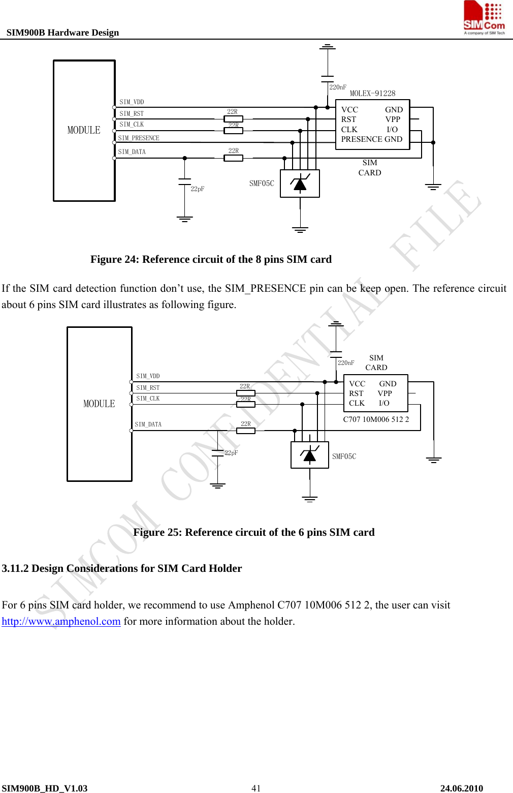
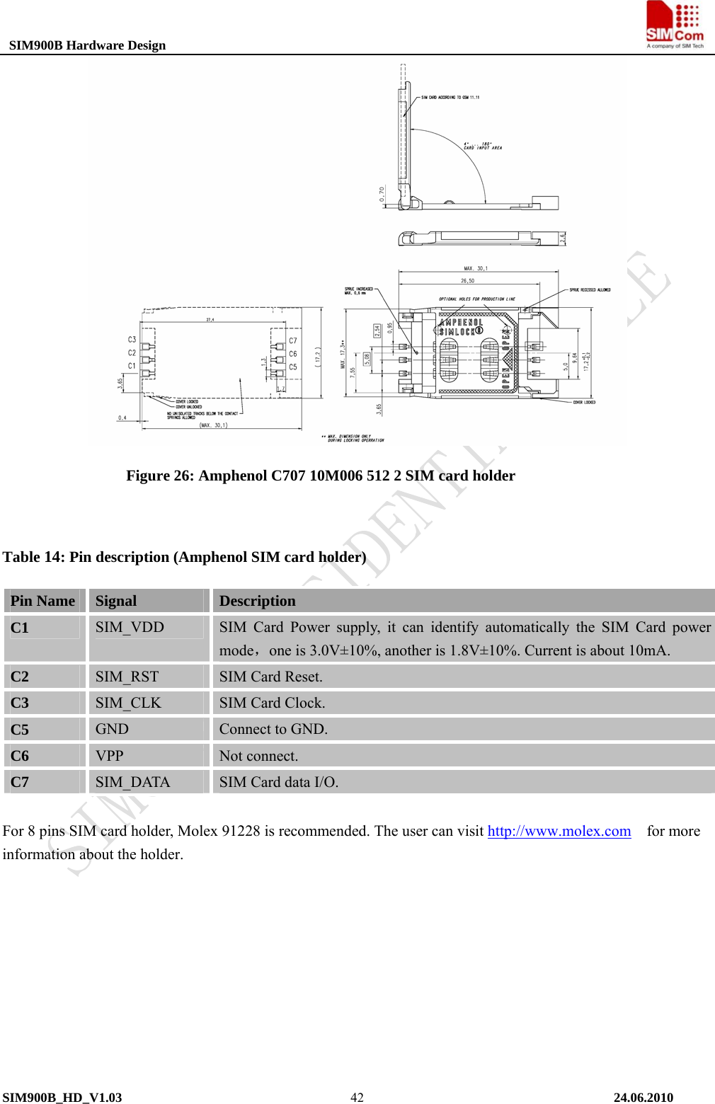
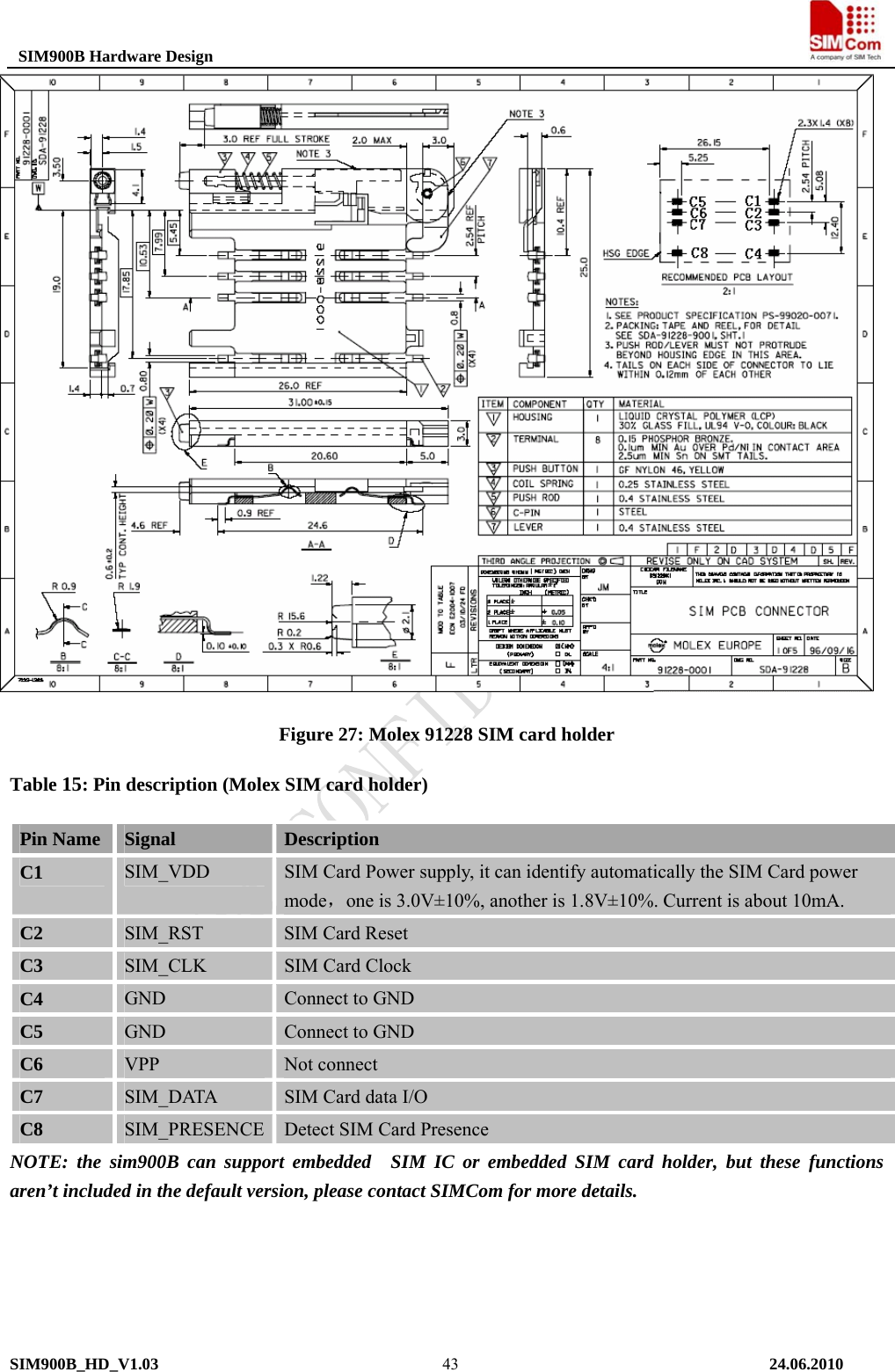
![SIM900B Hardware Design 3.11 SIM Card Interface 3.11.1 SIM Card Application The user can use AT Command to get information in SIM card. For more information, please refer to document [1]. The SIM interface supports the functionality of the GSM Phase 1 specification and also supports the functionality of the new GSM Phase 2+ specification for FAST 64 kbps SIM (intended for use with a SIM application Tool-kit). Both 1.8V and 3.0V SIM Cards are supported. The SIM interface is powered from an internal regulator in the module having normal voltage 3V. All pins reset as outputs driving low. Logic levels are as described in table Table 13: Pin define of the SIM interface Name Pin Function SIM_VDD 19 SIM Card Power output automatic output on SIM mode,one is 3.0V±10%, another is 1.8V±10%. Current is about 10mA. SIM_DATA 21 SIM Card data I/O SIM_CLK 23 SIM Card Clock SIM_RST 25 SIM Card Reset SIM_PRESENCE 16 SIM Card Presence Following is the reference circuit about SIM interface. We recommend an Electro-Static discharge device ST (www.st.com ) ESDA6V1W5 or ON SEMI (www.onsemi.com ) SMF05C for “ESD ANTI”. The 22Ω resistors showed in the following figure should be added in series on the IO line between the module and the SIM card for protecting the SIM I/O port. The pull up resistor (about 15KΩ) on the SIM_DATA line already added in the module. Note that the SIM peripheral circuit should be close to the SIM card socket. The SIM_PRESENCE pin is used for detecting the SIM card insert or removal. The user can use the AT command “AT+CSDT” to set the SIMCARD configuration. For detail of this AT command, please refer to document [1]: 8 pins SIM card holder can be selected . The reference circuit about 8 pins SIM card holder illustrates as following figure. SIM900B_HD_V1.03 24.06.2010 40](https://usermanual.wiki/Simcom/1005242010007.User-Manual/User-Guide-1319262-Page-40.png)
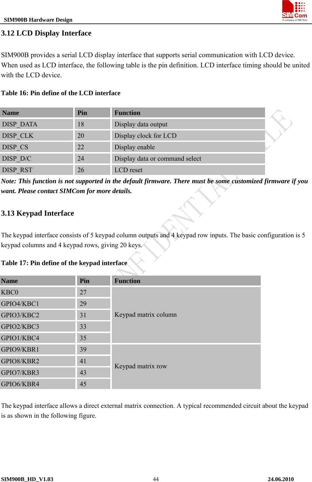
![SIM900B Hardware Design KBR4KBR3KBR2KBR1KBC0KBC1KBC2KBC3KBC4GNDMODULE Figure 28: Reference circuit of the keypad interface *Note: 1. This function is not supported in the default firmware. There must be customized firmware if you want. Please contact SIMCom for more details. 2.KBR0&KBC0 is used to power off the module, so do not connect them for other application. 3. keypad is the second function of this pin , the default function is GPIO. 3.14 ADC SIM900B provides one auxiliary ADC (General purpose analog to digital converter.) as voltage input pin, which can be used to detect the values of some external items such as voltage, temperature etc. We can use AT command “AT+CADC” to read the voltage value on ADC. For detail of this AT command, please refer to document [1]. Table 18: ADC specification MIN Type MAX Units Voltage range 0 - 2.8 V ADC Resolution - 10 - bits Sampling rate - - 200K Hz SIM900B_HD_V1.03 24.06.2010 45](https://usermanual.wiki/Simcom/1005242010007.User-Manual/User-Guide-1319262-Page-45.png)
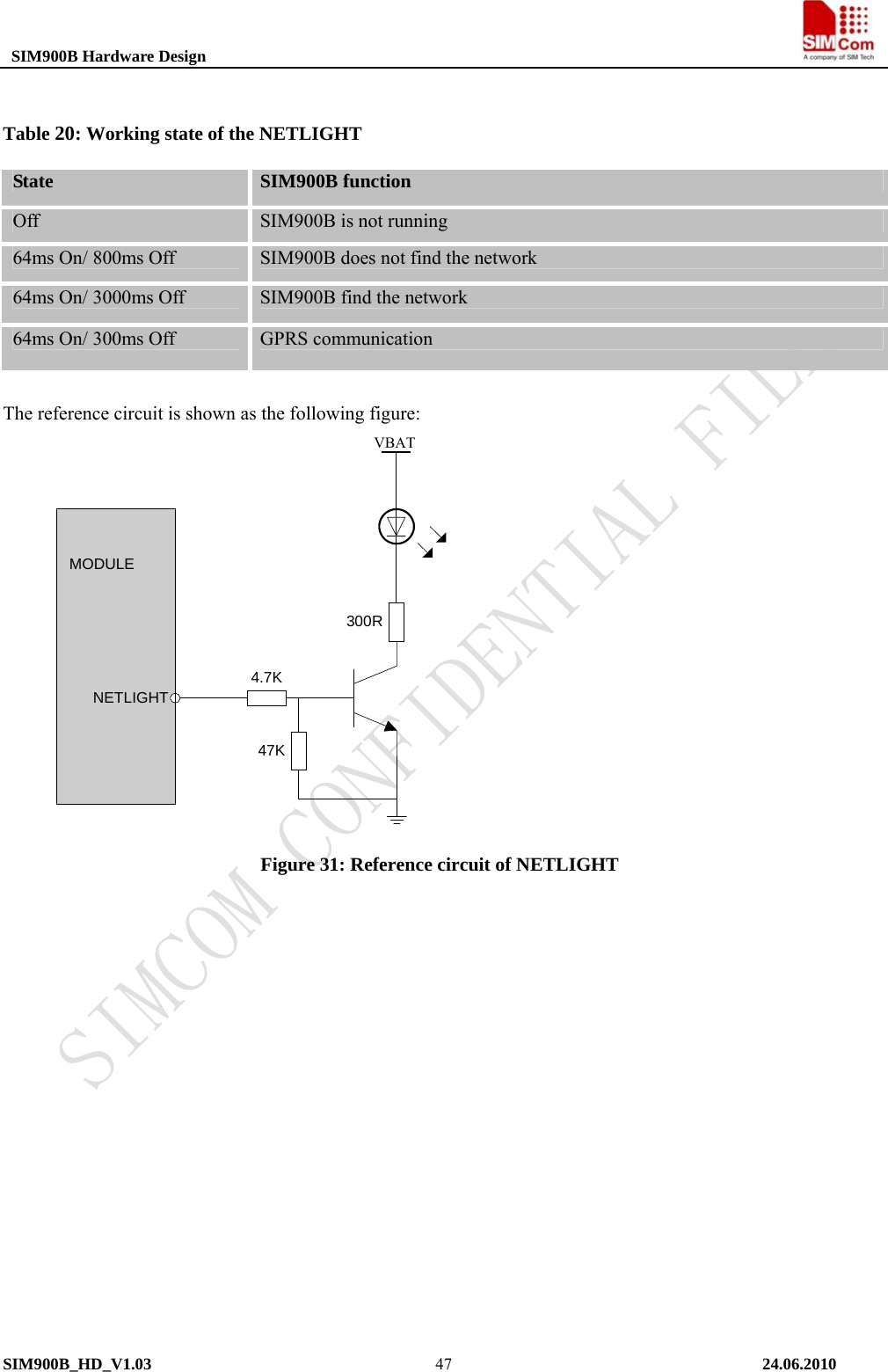
![SIM900B Hardware Design 3.15 Behaviors of the RI Table 19: Behaviours of the RI State RI respond Standby HIGH Voice calling Change LOW, then: (1)Change to HIGH when establish calling. (2)Use AT command ATH, the RI pin changes to HIGH. (3)Sender hangs up, change to HIGH. Data calling Change LOW, then: (1)Change to HIGH when establish calling. (2)Use AT command ATH, the RI changes to HIGH. SMS When receive SMS, The RI will change to LOW and hold low level about 120 ms, then change to HIGH. URC Some URCs triggers 120ms low level on RI. For more details, please refer to document [10] If the module is used as caller, the RI will maintain high. However, when it is used as receiver, following is timing of ring. Power on Ring MO or MT Hang upRing Hang on(talking)MO or MTHang upRing RI HIGHLOW Figure 29: SIM900B Services as Receiver RIPower on calling Hang up Echo talking calling Echo Hang up HIGHLOW Figure 30: SIM900B Services as caller 3.16 Network Status Indication The NETLIGHT can be used to drive a network status indication LED lamp. The working state of this pin is listed in following table: SIM900B_HD_V1.03 24.06.2010 46](https://usermanual.wiki/Simcom/1005242010007.User-Manual/User-Guide-1319262-Page-46.png)