Simcom 1005242010007 SIM900B Wireless Module User Manual
Shanghai Simcom Ltd. SIM900B Wireless Module
Simcom >
Contents
- 1. Mounting Information
- 2. User Manual
- 3. Users Manual
User Manual
a
Hardware Design
SIM900B_HD_V1.03
SIM900B Hardware Design
Document Title: SIM900B Hardware Design
Version: 1.03
Date: 2010-06-24
Status: Release
Document Control ID: SIM900B_HD_V1.03
General Notes
SIMCom offers this information as a service to its customers, to support application and engineering efforts
that use the products designed by SIMCom. The information provided is based upon requirements
specifically provided to SIMCom by the customers. SIMCom has not undertaken any independent search for
additional relevant information, including any information that may be in the customer’s possession.
Furthermore, system validation of this product designed by SIMCom within a larger electronic system
remains the responsibility of the customer or the customer’s system integrator. All specifications supplied
herein are subject to change.
Copyright
This document contains proprietary technical information which is the property of SIMCom Limited,
copying of this document and giving it to others and the using or communication of the contents thereof, are
forbidden without express authority. Offenders are liable to the payment of damages. All rights reserved in
the event of grant of a patent or the registration of a utility model or design. All specification supplied herein
are subject to change without notice at any time.
Copyright © Shanghai SIMCom Wireless Solutions Ltd. 2010
SIM900B_HD_V1.03 24.06.2010
2

SIM900B Hardware Design
Contents
Contents .....................................................................................................................................................................3
Version history...........................................................................................................................................................7
1 Introduction.............................................................................................................................................................8
1.1 Related Documents .......................................................................................................................................8
1.2 Terms and Abbreviations...............................................................................................................................8
1.3 Safety Caution.............................................................................................................................................11
2 SIM900B Overview ..............................................................................................................................................13
2.1 SIM900B Key Features...............................................................................................................................13
2.2 SIM900B Functional Diagram ....................................................................................................................15
2.3 SIM900B Evaluation Board ........................................................................................................................16
3 Application Interface.............................................................................................................................................18
3.1 SIM900B Pin Description ...........................................................................................................................18
3.2 Operating Modes.........................................................................................................................................21
3.3 Power Supply ..............................................................................................................................................22
3.3.1 Power Supply Pins.............................................................................................................................23
3.3.2 Minimizing Power Losses .................................................................................................................24
3.3.3 Monitoring Power Supply .................................................................................................................24
3.4 Power Up and Power Down Scenarios........................................................................................................24
3.4.1 Turn on SIM900B..............................................................................................................................24
3.4.2 Turn Off SIM900B............................................................................................................................26
3.4.3 Restart SIM900B Using the PWRKEY Pin.......................................................................................28
3.5 Power Saving ..............................................................................................................................................28
3.5.1 Minimum Functionality Mode ..........................................................................................................28
3.5.2 Sleep Mode (Slow Clock Mode) .......................................................................................................29
3.5.3 Wake Up SIM900B from SLEEP Mode ...........................................................................................29
3.6 Summary of State Transitions (except SLEEP mode).................................................................................29
3.7 RTC Backup ................................................................................................................................................30
3.8 Serial Interfaces...........................................................................................................................................31
3.8.1 Function of serial port & debug port supporting ...............................................................................33
3.8.2 Software Upgrade and Software Debug ............................................................................................34
3.9 Audio Interfaces ..........................................................................................................................................35
3.9.1 Speaker Interface Configuration........................................................................................................36
3.9.2 Microphone Interfaces Configuration ...............................................................................................37
3.9.3 Earphone Interface Configuration .....................................................................................................37
3.9.4 Referenced Electronic Characteristic ................................................................................................38
3.10 Buzzer .......................................................................................................................................................39
3.11 SIM Card Interface....................................................................................................................................40
3.11.1 SIM Card Application .....................................................................................................................40
3.11.2 Design Considerations for SIM Card Holder ..................................................................................41
SIM900B_HD_V1.03 24.06.2010
3

SIM900B Hardware Design
3.12 LCD Display Interface ..............................................................................................................................44
3.13 Keypad Interface .......................................................................................................................................44
3.14 ADC ..........................................................................................................................................................45
3.15 Behaviors of the RI ...................................................................................................................................46
3.16 Network Status Indication.........................................................................................................................46
3.17 General Purpose Input Output (GPIO)......................................................................................................48
4 Antenna Interface ..................................................................................................................................................49
4.1 Module RF Output Power ...........................................................................................................................50
4.2 Module RF Receive Sensitivity...................................................................................................................50
4.3 Module Operating Frequencies ...................................................................................................................50
5 Electrical, Reliability and Radio Characteristics...................................................................................................50
5.1 Absolute Maximum Ratings........................................................................................................................50
5.2 Operating Temperatures..............................................................................................................................51
5.3 Power Supply Ratings .................................................................................................................................51
5.4 Current Consumption ..................................................................................................................................52
5.5 Electro-Static Discharge..............................................................................................................................53
6 Mechanics .............................................................................................................................................................55
6.1 Mechanical Dimensions of SIM900B .........................................................................................................55
6.2 Top View of the SIM900B ..........................................................................................................................56
6.3 Mounting SIM900B onto the application platform.....................................................................................57
6.4 Board-to-board connector ...........................................................................................................................57
6.4.1 Mechanical dimensions of the SUNCAGEY BB530-06001-20R.....................................................57
6.5 RF connector ...............................................................................................................................................59
6.6 PIN Assignment of SIM900B .....................................................................................................................61
SIM900B_HD_V1.03 24.06.2010
4

SIM900B Hardware Design
Table Index
TABLE 1: RELATED DOCUMENTS............................................................................................................................... 8
TABLE 2: TERMS AND ABBREVIATIONS ................................................................................................................... 8
TABLE 3: SIM900B KEY FEATURES ........................................................................................................................... 13
TABLE 4: CODING SCHEMES AND MAXIMUM NET DATA RATES OVER AIR INTERFACE ............................ 15
TABLE 5: PIN DESCRIPTION ....................................................................................................................................... 18
TABLE 6: OVERVIEW OF OPERATING MODES........................................................................................................ 21
TABLE 7: PIN DEFINITION OF THE SERIAL INTERFACES .................................................................................... 31
TABLE 8: LOGIC LEVELS OF THE SERIAL PORT AND DEBUG PORT ................................................................. 32
TABLE 9: PIN DEFINE OF THE AUDIO INTERFACE ................................................................................................ 35
TABLE 10: MIC INPUT CHARACTERISTICS ............................................................................................................. 38
TABLE 11: AUDIO OUTPUT CHARACTERISTICS .................................................................................................... 38
TABLE 12: BUZZER OUTPUT CHARACTERISTICS ................................................................................................. 39
TABLE 13: PIN DEFINE OF THE SIM INTERFACE.................................................................................................... 40
TABLE 14: PIN DESCRIPTION (AMPHENOL SIM CARD HOLDER) ...................................................................... 42
TABLE 15: PIN DESCRIPTION (MOLEX SIM CARD HOLDER) .............................................................................. 43
TABLE 16: PIN DEFINE OF THE LCD INTERFACE................................................................................................... 44
TABLE 17: PIN DEFINE OF THE KEYPAD INTERFACE........................................................................................... 44
TABLE 18: ADC SPECIFICATION ................................................................................................................................45
TABLE 19: BEHAVIOURS OF THE RI.......................................................................................................................... 46
TABLE 20: WORKING STATE OF THE NETLIGHT ................................................................................................... 47
TABLE 21: PIN DEFINE OF THE GPIO INTERFACE ................................................................................................. 48
TABLE 22: SIM900B CONDUCTED RF OUTPUT POWER........................................................................................ 50
TABLE 23: SIM900B CONDUCTED RF RECEIVE SENSITIVITY ............................................................................ 50
TABLE 24: SIM900B OPERATING FREQUENCIES.................................................................................................... 50
TABLE 25: ABSOLUTE MAXIMUM RATINGS........................................................................................................... 51
TABLE 26: SIM900B OPERATING TEMPERATURE .................................................................................................. 51
TABLE 27: SIM900B POWER SUPPLY RATINGS....................................................................................................... 51
TABLE 28: SIM900B CURRENT CONSUMPTION(VBAT=3.8V)......................................................................... 52
TABLE 29: THE ESD ENDURE STATUE MEASURED TABLE (TEMPERATURE: 25℃, HUMIDITY:45% ) ........ 53
TABLE 30: PIN ASSIGNMENT...................................................................................................................................... 61
SIM900B_HD_V1.03 24.06.2010
5

SIM900B Hardware Design
Figure Index
FIGURE 1: SIM900B FUNCTIONAL DIAGRAM......................................................................................................... 16
FIGURE 2: TOP VIEW OF SIM900B EVB .................................................................................................................... 17
FIGURE 3: REFERENCE CIRCUIT OF THE VBAT INPUT ........................................................................................ 22
FIGURE 4: REFERENCE CIRCUIT OF THE SOURCE POWER SUPPLY INPUT..................................................... 23
FIGURE 5: VBAT VOLTAGE DROP DURING TRANSMIT BURST........................................................................... 23
FIGURE 6: TURN ON SIM900B USING DRIVING CIRCUIT..................................................................................... 25
FIGURE 7: TURN ON SIM900B USING BUTTON ...................................................................................................... 25
FIGURE 8: TIMING OF TURN ON SYSTEM USING PWRKEY ................................................................................ 26
FIGURE 9: TIMING OF TURN OFF SYSTEM USING PWRKEY............................................................................... 26
FIGURE 10: TIMING OF RESTART SYSTEM ............................................................................................................. 28
FIGURE 11: STATE TRANSITION ................................................................................................................................29
FIGURE 12: RTC SUPPLY FROM NON-CHARGEABLE BATTERY ......................................................................... 30
FIGURE 13: RTC SUPPLY FROM RECHARGEABLE BATTERY .............................................................................. 30
FIGURE 14: RTC SUPPLY FROM CAPACITOR .......................................................................................................... 31
FIGURE 15: SEIKO XH414H-IV01E CHARGE CHARACTERISTIC ......................................................................... 31
FIGURE 16: CONNECTION OF THE SERIAL INTERFACES..................................................................................... 33
FIGURE 17: CONNECTION OF SOFTWARE UPGRADE AND SOFTWARE DEBUG ............................................. 34
FIGURE 18: RS232 LEVEL CONVERTER CIRCUIT................................................................................................... 35
FIGURE 19: SPEAKER INTERFACE CONFIGURATION ........................................................................................... 36
FIGURE 20: SPEAKER INTERFACE WITH AMPLIFIER CONFIGURATION .......................................................... 36
FIGURE 21: MICROPHONE INTERFACE CONFIGURATION................................................................................... 37
FIGURE 22: EARPHONE INTERFACE CONFIGURATION........................................................................................ 37
FIGURE 23: REFERENCE CIRCUIT OF BUZZER ...................................................................................................... 39
FIGURE 24: REFERENCE CIRCUIT OF THE 8 PINS SIM CARD.............................................................................. 41
FIGURE 25: REFERENCE CIRCUIT OF THE 6 PINS SIM CARD.............................................................................. 41
FIGURE 26: AMPHENOL C707 10M006 512 2 SIM CARD HOLDER........................................................................ 42
FIGURE 27: MOLEX 91228 SIM CARD HOLDER ...................................................................................................... 43
FIGURE 28: REFERENCE CIRCUIT OF THE KEYPAD INTERFACE ....................................................................... 45
FIGURE 29: SIM900B SERVICES AS RECEIVER ....................................................................................................... 46
FIGURE 30: SIM900B SERVICES AS CALLER ........................................................................................................... 46
FIGURE 31: REFERENCE CIRCUIT OF NETLIGHT .................................................................................................. 47
FIGURE 32 : THE RF INTERFACE OF MODULE ....................................................................................................... 49
FIGURE 33: TOP AN SIDE MECHANICAL DIMENSIONS OF MODULE (UNIT: MM).................................... 55
FIGURE 34:MECHANICAL DIMENSIONS OF MODULE PCB DECAL(UNIT: MM)...................................... 56
FIGURE 35: TOP VIEW OF THE SIM900B................................................................................................................... 56
FIGURE 36: SUNCAGEY BB530-06001-20R BOARD-TO-BOARD CONNECTOR.................................................. 57
FIGURE 37 BOARD-TO-BOARD CONNECTOR PHYSICAL PHOTO ...................................................................... 58
FIGURE 38: U.FL-R-SMT............................................................................................................................................... 59
FIGURE 39: U.FL SERIES RF ADAPTER CABLE ....................................................................................................... 60
SIM900B_HD_V1.03 24.06.2010
6

SIM900 Hardware Design
Version history
Date Version Description of change Author
2010-04-08 1.01 Origin Huangqiuju
2010-05-31 1.02 Modify voltage domain ,current consumption and
figure37 Huangqiuju
2010-06-23 1.03 §2.1, §3.3. §3.4 Modify the power supply range from
3.2V~4.8V to 3.1V~4.8V
§3.7, Modify the VRTC pin connection when RTC
backup is not needed.
Huangqiuju
SIM900_HD_V1.03 7 24.06.2010
SIM900B Hardware Design
1 Introduction
This document describes the hardware interface of the SIMCom SIM900B module that connects to the specific
application and the air interface. As SIM900B can be integrated with a wide range of applications, all functional
components of SIM900B are described in great detail.
This document can help you quickly understand SIM900B interface specifications, electrical and mechanical
details. With the help of this document and other SIM900B application notes, user guide, the user can use
SIM900B module to design and set-up mobile applications quickly.
1.1 Related Documents
Table 1: Related documents
SN Document name Remark
[1] SIM900_ATC SIM900_ATC
[2] ITU-T Draft new
recommendation
V.25ter:
Serial asynchronous automatic dialing and control
[3] GSM 07.07: Digital cellular telecommunications (Phase 2+); AT command set for GSM
Mobile Equipment (ME)
[4] GSM 07.10: Support GSM 07.10 multiplexing protocol
[5] GSM 07.05: Digital cellular telecommunications (Phase 2+); Use of Data Terminal
Equipment – Data Circuit terminating Equipment (DTE – DCE) interface for
Short Message Service (SMS) and Cell Broadcast Service (CBS)
[6] GSM 11.14: Digital cellular telecommunications system (Phase 2+); Specification of the SIM
Application Toolkit for the Subscriber Identity Module – Mobile Equipment
(SIM – ME) interface
[7] GSM 11.11: Digital cellular telecommunications system (Phase 2+); Specification of the
Subscriber Identity Module – Mobile Equipment (SIM – ME) interface
[8] GSM 03.38: Digital cellular telecommunications system (Phase 2+); Alphabets and
language-specific information
[9] GSM 11.10 Digital cellular telecommunications system (Phase 2); Mobile Station (MS)
conformance specification; Part 1: Conformance specification
[10] AN_Serial Port AN_Serial Port
1.2 Terms and Abbreviations
Table 2: Terms and Abbreviations
SIM900B_HD_V1.03 24.06.2010
8

SIM900B Hardware Design
Abbreviation Description
ADC Analog-to-Digital Converter
AMR Adaptive Multi-Rate
ARP Antenna Reference Point
ASIC Application Specific Integrated Circuit
BER Bit Error Rate
BTS Base Transceiver Station
CHAP Challenge Handshake Authentication Protocol
CS Coding Scheme
CSD Circuit Switched Data
CTS Clear to Send
DAC Digital-to-Analog Converter
DRX Discontinuous Reception
DSP Digital Signal Processor
DTE Data Terminal Equipment (typically computer, terminal, printer)
DTR Data Terminal Ready
DTX Discontinuous Transmission
EFR Enhanced Full Rate
EGSM Enhanced GSM
EMC Electromagnetic Compatibility
ESD Electrostatic Discharge
ETS European Telecommunication Standard
FCC Federal Communications Commission (U.S.)
FDMA Frequency Division Multiple Access
FR Full Rate
GMSK Gaussian Minimum Shift Keying
GPRS General Packet Radio Service
GSM Global Standard for Mobile Communications
HR Half Rate
I/O Input/Output
IC Integrated Circuit
IMEI International Mobile Equipment Identity
kbps Kilo bits per second
LED Light Emitting Diode
Li-Ion Lithium-Ion
MO Mobile Originated
MS Mobile Station (GSM engine), also referred to as TE
MT Mobile Terminated
SIM900B_HD_V1.03 24.06.2010
9

SIM900B Hardware Design
Abbreviation Description
PAP Password Authentication Protocol
PBCCH Packet Switched Broadcast Control Channel
PCB Printed Circuit Board
PCS Personal Communication System, also referred to as GSM 1900
PDU Protocol Data Unit
PPP Point-to-point protocol
RF Radio Frequency
RMS Root Mean Square (value)
RTC Real Time Clock
RX Receive Direction
SIM Subscriber Identification Module
SMS Short Message Service
TDMA Time Division Multiple Access
TE Terminal Equipment, also referred to as DTE
TX Transmit Direction
UART Universal Asynchronous Receiver & Transmitter
URC Unsolicited Result Code
USSD Unstructured Supplementary Service Data
VSWR Voltage Standing Wave Ratio
Vmax Maximum Voltage Value
Vnorm Normal Voltage Value
Vmin Minimum Voltage Value
VIHmax Maximum Input High Level Voltage Value
VIHmin Minimum Input High Level Voltage Value
VILmax Maximum Input Low Level Voltage Value
VILmin Minimum Input Low Level Voltage Value
VImax Absolute Maximum Input Voltage Value
VImin Absolute Minimum Input Voltage Value
VOHmax Maximum Output High Level Voltage Value
VOHmin Minimum Output High Level Voltage Value
VOLmax Maximum Output Low Level Voltage Value
VOLmin Minimum Output Low Level Voltage Value
Inorm Normal Current
Imax Maximum Load Current
SIM900B_HD_V1.03 24.06.2010
10
SIM900B Hardware Design
Phonebook abbreviations
Abbreviation Description
FD SIM fix dialing phonebook
LD SIM last dialing phonebook (list of numbers most recently dialed)
MC Mobile Equipment list of unanswered MT calls (missed calls)
ON SIM (or ME) own numbers (MSISDNs) list
RC Mobile Equipment list of received calls
SM SIM phonebook
NC Not connect
1.3 Safety Caution
The following safety precautions must be observed during all phases of the operation. Usage, service or repair of
any cellular terminal or mobile incorporating SIM900B module. Manufactures of the cellular terminal should send
words the following safety information to users and operating personnel and to incorporate these guidelines into
all manuals supplied with the product. If not so, SIMCom does not take on any liability for customer failure to
comply with these precautions.
When in a hospital or other health care facility, observe the restrictions about the
use of mobiles. Switch the cellular terminal or mobile off, medical equipment may be sensitive
to not operate normally for RF energy interference.
Switch off the cellular terminal or mobile before boarding an aircraft. Make sure it be switched
off. The operation of wireless appliances in an aircraft is forbidden to prevent interference with
communication systems. Forget to think much of these instructions may lead to the flight safety
or offend against local legal action, or both.
Do not operate the cellular terminal or mobile in the presence of flammable gases or fumes.
Switch off the cellular terminal when you are near petrol stations, fuel depots, chemical plants or
where blasting operations are in progress. Operation of any electrical equipment in potentially
explosive atmospheres can constitute a safety hazard.
Your cellular terminal or mobile receives and transmits radio frequency energy while switched
on. RF interference can occur if it is used close to TV sets, radios, computers or other electric
equipment.
SIM900B_HD_V1.03 24.06.2010
11
SIM900B Hardware Design
Road safety comes first! Do not use a hand-held cellular terminal or mobile when driving a
vehicle, unless it is securely mounted in a holder for hands free operation. Before making a
call with a hand-held terminal or mobile, park the vehicle.
GSM cellular terminals or mobiles operate over radio frequency signals and cellular networks
and cannot be guaranteed to connect in all conditions, for example no mobile fee or a invalid
SIM card. While you are in this condition and need emergent help, Please Remember using
emergency calls. In order to make or receive calls, the cellular terminal or mobile must be
switched on and in a service area with adequate cellular signal strength.
Some networks do not allow for emergency call if certain network services or phone features are
in use (e.g. lock functions, fixed dialing etc.). You may
have to deactivate those features before you can make an emergency call.
Also, some networks require that a valid SIM card be properly inserted in the cellular terminal
or mobile.
SIM900B_HD_V1.03 24.06.2010
12

SIM900B Hardware Design
2 SIM900B Overview
Designed for global market, SIM900B is a quad-band GSM/GPRS engine that works on frequencies GSM
850MHz, EGSM 900MHz, DCS 1800MHz and PCS 1900MHz. SIM900B features GPRS multi-slot class 10/
class 8 (optional) and supports the GPRS coding schemes CS-1, CS-2, CS-3 and CS-4.
With a tiny configuration of 40mm x 33mm x 3mm, SIM900B can meet almost all the space requirements in your
applications, such as M2M, smart phone, PDA and other mobile devices.
The physical interface to the mobile application is a 60-pin board-to-board connector, which provides all
hardware interfaces between the module and customers’ boards except the RF antenna interface.
z The keypad and SPI display interface will give you the flexibility to develop customized applications.
z Serial port and Debug port can help you easily develop your applications.
z Two audio channels include a microphone input and a speaker output.
z Programmable general purpose input & output.
The SIM900B is designed with power saving technique so that the current consumption is as low as 1.2mA in
SLEEP mode.
The SIM900B is integrated with the TCP/IP protocol; extended TCP/IP AT commands are developed for
customers to use the TCP/IP protocol easily, which is very useful for those data transfer applications.
2.1 SIM900B Key Features
Table 3: SIM900B key features
Feature Implementation
Power supply Single supply voltage :3.1V – 4.8V
Power saving Typical power consumption in SLEEP mode is 1.2mA ( BS-PA-MFRMS=5)
Frequency Bands
z Quad-band: GSM 850, EGSM 900, DCS 1800, PCS 1900. The SIM900B can
search the 4 frequency bands automatically. The frequency bands also can be
set by AT command.
z Compliant to GSM Phase 2/2+
GSM class Small MS
Transmitting power z Class 4 (2W) at GSM 850 and EGSM 900
z Class 1 (1W) at DCS 1800 and PCS 1900
GPRS connectivity
z GPRS multi-slot class 10 (default)
z GPRS multi-slot class 8 (option)
z GPRS mobile station class B
SIM900B_HD_V1.03 24.06.2010
13

SIM900B Hardware Design
Temperature range
z Normal operation: -30°C to +80°C
z Restricted operation: -40°C to -30°C and +80 °C to +85°C(1)
z Storage temperature -45°C to +90°C
DATA GPRS:
CSD:
z GPRS data downlink transfer: max. 85.6 kbps
z GPRS data uplink transfer: max. 42.8 kbps
z Coding scheme: CS-1, CS-2, CS-3 and CS-4
z Supports the protocols PAP (Password Authentication Protocol) usually used
for PPP connections.
z Integrates the TCP/IP protocol.
z Support Packet Switched Broadcast Control Channel (PBCCH)
z CSD transmission rates: 2.4, 4.8, 9.6, 14.4 kbps, non-transparent
z Unstructured Supplementary Services Data (USSD) support
SMS z MT, MO, CB, Text and PDU mode
z SMS storage: SIM card
FAX Group 3 Class 1
SIM interface Support SIM card: 1.8V, 3V
External antenna Connected via 50 Ohm antenna connector or antenna pad
Audio features Speech codec modes:
z Half Rate (ETS 06.20)
z Full Rate (ETS 06.10)
z Enhanced Full Rate (ETS 06.50 / 06.60 / 06.80)
z Adaptive multi rate (AMR)
z Echo Cancellation
z Noise Suppression
Serial port and
Debug port
Serial Port:
z 7-wire modem interface with status and control lines, unbalanced,
asynchronous.
z 1200bps to 115200bps.
z Serial Port can be used for AT commands or data stream.
z Supports RTS/CTS hardware handshake and software ON/OFF flow control.
z Multiplex ability according to GSM 07.10 Multiplexer Protocol.
z Autobauding supports baud rate from 1200 bps to 57600bps.
Debug port:
z 2-wire interface DBG_TXD and DBG_RXD.
z Can be used for debugging and firmware upgrade.
Phonebook management Support phonebook types: SM, FD, LD, RC, ON, MC.
SIM Application Toolkit Support SAT class 3, GSM 11.14 Release 99
Real time clock Implemented
Timer function Programmable via AT command
Physical characteristics Size: 40mm x 33mm x 3.0mm
Weight: 7g
Firmware upgrade Firmware upgrade over debug port.
SIM900B_HD_V1.03 24.06.2010
14
SIM900B Hardware Design
(1) The SIM900B does work, but deviations from the GSM specification may occur.
Table 4: Coding schemes and maximum net data rates over air interface
Coding scheme 1 Timeslot 2 Timeslot 4 Timeslot
CS-1: 9.05kbps 18.1kbps 36.2kbps
CS-2: 13.4kbps 26.8kbps 53.6kbps
CS-3: 15.6kbps 31.2kbps 62.4kbps
CS-4: 21.4kbps 42.8kbps 85.6kbps
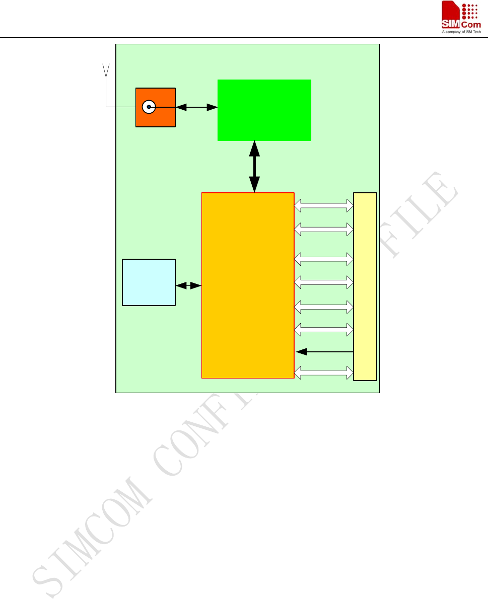
2.2 SIM900B Functional Diagram
The following figure shows a functional diagram of the SIM900B and illustrates the mainly functional part:
z The GSM baseband engine
z Flash and SRAM
z The GSM radio frequency part
z The antenna interface
z The board-to-board interface
z The Other interfaces
SIM900B_HD_V1.03 24.06.2010
15
SIM900B Hardware Design
Flash+
SRAM Baseband
Engine
Radio
Frequency
Board-to-board Connector
LCD
KEYPADS
AUDIO
SIM
ADC
UART
GPIO
POWER
SIM 900B
Antenna
connector
Figure 1: SIM900B functional diagram
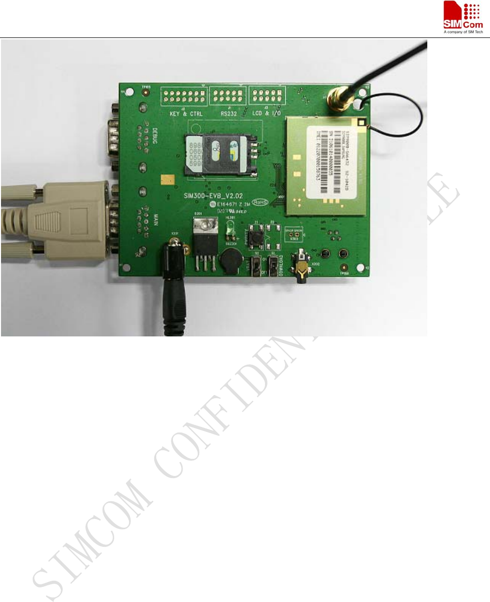
2.3 SIM900B Evaluation Board
In order to help you on the application of SIM900B, SIMCom can supply an Evaluation Board (EVB) that
interfaces the SIM900B directly with appropriate power supply, SIM card holder, RS232 serial port, handset port,
earphone port, antenna and all GPIO of the SIM900B.
SIM900B_HD_V1.03 24.06.2010
16
SIM900B Hardware Design
SIM900B_HD_V1.03 24.06.2010
17
Figure 2: Top view of SIM900B EVB
For details please refer to the SIM900B-EVB_UGD document.

SIM900B Hardware Design
3 Application Interface
SIM900B is equipped with a 60-pin 0.5mm pitch board-to-board connector that connects to the cellular
application platform. Sub-interfaces included in this board-to-board connector are described in detail in following
chapters:
z Power supply (please refer to Chapter 3.3)
z Serial interfaces (please refer to Chapter 3.8)
z Analog audio interfaces (please refer to Chapter 3.9)
z SIM interface (please refer to Chapter 3.11)
Electrical and mechanical characteristics of the board-to-board connector are specified in Chapter 6. There we also
include order information for mating connectors.
3.1 SIM900B Pin Description
Table 5: Pin description
Power Supply
PIN NAME I/O DESCRIPTION DC CHARACTERISTICS COMMENT
VBAT I 8 VBAT pins are dedicated to
connect the supply voltage.
The power supply of SIM900B
has to be a single voltage
source of VBAT= 3.2V...4.8V.
It must be able to provide
sufficient current in a transmit
burst which typically rises to
2A
Vmax= 4.8V
Vmin=3.1V
Vnorm=4.0V
VRTC I/O Current input for RTC when
the battery is not supplied for
the system.
Current output for backup
battery when the main battery
is present and the backup
battery is in low voltage state.
Vmax=3.15V
Vmin=2.0V
Vnorm=3.0V
Iout(max)= 200uA
Iin=3 uA
If the RTC function
is enabled, a
backup battery or
capacitor should be
connected to the
VRTC pin.
Otherwise connect
a 4.7uF capacitor
to the VRTC pin.
VDD_EXT O 2.8V output power supply Vmax=2.95V
Vmin=2.70V
Vnorm=2.80V
If unused, keep
open.
SIM900B_HD_V1.03 24.06.2010
18

SIM900B Hardware Design
Iout(max)= 10mA
GND Ground
Power on or power off
PIN NAME I/O DESCRIPTION DC CHARACTERISTICS
PWRKEY I Power on/off detect, active low. VILmax=0.9V
VIHmin=2.6V
VImax=3.3V
VILmin= 0V
It is already pulled
up internally (3V).
Audio interfaces
PIN NAME I/O DESCRIPTION DC CHARACTERISTICS COMMENT
MIC1P
MIC1N
I Positive and negative
voice-band input
MIC2P
MIC2N
I Auxiliary positive and negative
voice-band input
If unused keep
open
SPK1P
SPK1N
O Positive and negative
voice-band output
SPK2P
SPK2N
O Auxiliary positive and negative
voice-band output
Audio DC Characteristics
refer to chapter 3.9.4
If unused keep
open
AGND Analog ground Separate ground
connection for
external audio
circuits.
If unused keep
open.
Display interface
PIN NAME I/O DESCRIPTION DC CHARACTERISTICS COMMENT
DISP_RST O
DISP_DATA I/O
DISP _CLK O
DISP _CS O
DISP _D/C O
Display interface VILmax=0.15 *VDD_EXT
VIHmin=0.85*VDD_EXT
VILmin= 0V
VIHmax= VDD_EXT
VOHmin= VDD_EXT-0.1V
VOLmax=0.1V
VOHmax= VDD_EXT
VOLmin= 0V
If unused keep
open
General purpose input/output
GPIO1/ KBC4 I/O Default as GPIO,can be
multiplexed as keypad
VILmax=0.15 *VDD_EXT
VIHmin=0.85*VDD_EXT
If unused keep
open
SIM900B_HD_V1.03 24.06.2010
19

SIM900B Hardware Design
GPIO2/ KBC3 I/O
GPIO3/ KBC2 I/O
GPIO4/ KBC1 I/O
GPIO6/ KBR3 I/O
GPIO7/ KBR4 I/O
GPIO8/ KBR2 I/O
GPIO9/ KBR1 I/O
KBR0 I
KBC0 O
VILmin= 0V
VIHmax= VDD_EXT
VOHmin= VDD_EXT-0.1V
VOLmax=0.1V
VOHmax= VDD_EXT
VOLmin= 0V
Just for power
down, If unused
keep open
Serial port
PIN NAME I/O DESCRIPTION DC CHARACTERISTICS COMMENT
RXD I Receive data
TXD O Transmit data
RTS I Request to send
CTS O Clear to send
RI O Ring indicator
DCD O Data carry detect
DTR I Data terminal Ready
VILmax=0.15 *VDD_EXT
VIHmin=0.85*VDD_EXT
VILmin= 0V
VIHmax= VDD_EXT
VOHmin= VDD_EXT-0.1V
VOLmax=0.1V
VOHmax= VDD_EXT
VOLmin= 0V
DTR Pin has
been pulled up to
VDD_EXT
internally. If
unused keep
open
Debug interface
PIN NAME I/O DESCRIPTION DC CHARACTERISTICS COMMENT
DBG_TXD O
DBG_RXD I
Serial interface for debugging
and firmware upgrade
VILmax=0.15 *VDD_EXT
VIHmin=0.85*VDD_EXT
VILmin= 0V
VIHmax= VDD_EXT
VOHmin= VDD_EXT-0.1V
VOLmax=0.1V
VOHmax= VDD_EXT
VOLmin= 0V
If unused keep
open
SIM interface
PIN NAME I/O DESCRIPTION DC CHARACTERISTICS COMMENT
SIM_VDD O Voltage supply for SIM card The voltage can be select by
software automatically
either 1.8V or 3V
SIM_DATA I/O SIM data output VILmax=0.15 *SIM_VDD
SIM900B_HD_V1.03 24.06.2010
20
SIM900B Hardware Design
SIM_CLK O SIM clock
SIM_RST O SIM reset
VIHmin=0.85*SIM_VDD
VILmin= 0V
VIHmax= SIM_VDD
VOHmin= SIM_VDD-0.1V
VOLmax=0.1V
VOHmax= SIM_VDD
VOLmin= 0V
SIM_PRESENCE I SIM detect VILmax=0.15 *VDD_EXT
VIHmin=0.85*VDD_EXT
VILmin= 0V
VIHmax= VDD_EXT
If unused keep
open
ADC
PIN NAME I/O DESCRIPTION DC CHARACTERISTICS COMMENT
ADC0 I General purpose analog to
digital converter.
Input voltage range: 0V ~
2.8V
If unused keep
open
Pulse Width Modulation
PIN NAME I/O DESCRIPTION DC CHARACTERISTICS COMMENT
BUZZER O PWM Output VOHmin= VDD_EXT-0.1V
VOLmax=0.1V
VOHmax= VDD_EXT
VOLmin=0
If unused keep
open
3.2 Operating Modes
The table below briefly summarizes the various operating modes referred to in the following chapters.
Table 6: Overview of operating modes
Mode Function
GSM/GPRS
SLEEP
Module will automatically go into SLEEP mode if DTR is set to high level
and there is no on air and no hardware interrupt (such as GPIO interrupt or
data on serial port).
In this case, the current consumption of module will reduce to the minimal
level.
In SLEEP mode, the module can still receive paging message and SMS
from the BTS normally.
Normal
operation
GSM IDLE Software is active. Module has registered to the GSM network, and the
SIM900B_HD_V1.03 24.06.2010
21
SIM900B Hardware Design
module is ready to send and receive.
GSM TALK
Connection between two subscribers is in progress. In this case, the power
consumption depends on network settings such as DTX off/on,
FR/EFR/HR, hopping sequences, antenna.
GPRS
STANDBY
Module is ready for GPRS data transfer, but no data is currently sent or
received. In this case, power consumption depends on network settings and
GPRS configuration.
GPRS DATA There is GPRS data transfer (PPP or TCP or UDP) in progress. In this case,
power consumption is related with network settings (e.g. power control
level), uplink / downlink data rates and GPRS configuration (e.g. used
multi-slot settings).
POWER
DOWN
Normal shutdown by sending the “AT+CPOWD=1” command or using the PWRKEY. The
power management ASIC disconnects the power supply from the baseband part of the
module, and only the power supply for the RTC is remained. Software is not active. The
serial port is not accessible. Operating voltage (connected to VBAT) remains applied.
Minimum
functionality
mode (without
remove power
supply)
Use the “AT+CFUN” command can set the module to a minimum functionality mode
without remove the power supply. In this case, the RF part of the module will not work or the
SIM card will not be accessible, or both RF part and SIM card will be closed, and the serial
port is still accessible. The power consumption in this case is very low.
3.3 Power Supply
The power supply of SIM900B is from a single voltage source of VBAT= 3.1V...4.8V. In some case, the ripple in
a transmitting burst may cause voltage drops when current consumption rises to typical peaks of 2A. So the power
supply must be able to provide sufficient current up to 2A.
For the VBAT input, a local bypass capacitor is recommended. A capacitor (about 100 µF, low ESR) is
recommended. Multi-layer ceramic chip (MLCC) capacitors can provide the best combination of low ESR and
small size but may not be cost effective. A lower cost choice may be a 100 µF tantalum capacitor (low ESR) with
a small (0.1µF to 1µF) ceramic in parallel, which is illustrated as following figure. The capacitors should be
placed as close as possible to the SIM900B VBAT pins. The following figure is the recommended circuit.
CACB
VBAT
+
Figure 3: Reference circuit of the VBAT input
SIM900B_HD_V1.03 24.06.2010
22
SIM900B Hardware Design
The circuit design of the power supply depends strongly upon the power source where this power is drained. The
following figure is the reference design of +5V input source power supply. The designed output for the power
supply is 4.1V, thus a linear regulator can be used. If there’s a big difference between the input source and the
desired output (VBAT), a switching converter power supply will be preferable because of its better efficiency
especially with the 2A peak current in burst mode of the module.
A single 3.6V Li-Ion cell battery type can be connected to the power supply of the SIM900B VBAT directly. But
the Ni_Cd or Ni_MH battery types must be used carefully, since their maximum voltage can rise over the absolute
maximum voltage of the module and damage it.
Figure 4: Reference circuit of the source power supply input
The following figure is the VBAT voltage ripple wave at the maximum power transmit phase, the test condition is
VBAT=4.0V, VBAT maximum output current =2A, CA=100µF tantalum capacitor (ESR=0.7Ω) and CB=1µF.
Max:300mV
VBAT
Burst:2A
IVBAT
4.615ms
577us
Figure 5: VBAT voltage drop during transmit burst
3.3.1 Power Supply Pins
Eight VBAT pins of the board-to-board connector are dedicated to connect the supply voltage; six GND pins are
recommended for grounding. VRTC pin can be used to back up the RTC.
SIM900B_HD_V1.03 24.06.2010
23

SIM900B Hardware Design
3.3.2 Minimizing Power Losses
When designing the power supply for your application please pay specific attention to power losses. Ensure that
the input voltage VBAT never drops below 3.2V even in a transmit burst where current consumption can rise to
typical peaks of 2A. If the power voltage drops below 3.2V, the module may be switched off. The PCB traces
from the VBAT pins to the power source must be wide enough to decrease voltage drops in the transmitting burst
mode.
3.3.3 Monitoring Power Supply
To monitor the supply voltage, the user can use the “AT+CBC” command which include a parameter: voltage
value (in mV).
The voltage is continuously measured at intervals depending on the operating mode. The displayed voltage (in
mV) is averaged over the last measuring period before the “AT+CBC” command is executed.
For details please refer to document [1]
3.4 Power Up and Power Down Scenarios
In general, be sure not to turn on SIM900B while it is beyond the safety limits of voltage and temperature stated
in Chapter 3.4.2. SIM900B would immediately switch off after having started and detected these inappropriate
conditions. In extreme cases this can cause permanent damage to the module.
3.4.1 Turn on SIM900B
SIM900B can be turned on by the following way, which is described in following chapters:
z Via PWRKEY pin: starts normal operating mode (please refer to chapter 3.4.1.1);
Note: The AT command must be set after the SIM900B is power on and Unsolicited Result Code “RDY” is
received from the serial port. However if the SIM900B is set autobauding, the serial port will receive nothing.
The AT commands can be set after the SIM900B is power on. “AT+IPR=x” can be used to set a fixed baud
rate and save the configuration to non-volatile flash memory. After the configuration is saved as fixed baud
rate, the Code “RDY” should be received from the serial port all the time that the SIM900B is power on.
Please refer to the chapter “AT+IPR” in document [1].
3.4.1.1 Turn on SIM900B Using the PWRKEY Pin (Power on)
The SIM900B can be turn on by driving the PWRKEY to a low level voltage for some time and then release.
This pin has pulled up to a 3V voltage source in the module. The simple circuit illustrates as the following
figures.
SIM900B_HD_V1.03 24.06.2010
24
SIM900B Hardware Design
4.7k
47k
Turn on impulse
3V
1K
100K
POWERKEY
Module
Figure 6: Turn on SIM900B using driving circuit
S1
PWRKEY
TVS1
Figure 7: Turn on SIM900B using button
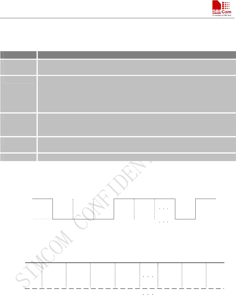
The power on scenarios illustrates as following figure.
VIL=1.2V
VIH > 2.55V
Pulldown >1s
VBAT
PWRKEY
(INPUT)
Delay > 2.2s
Serial Port Undefined Active
SIM900B_HD_V1.03 24.06.2010
25
SIM900B Hardware Design
Figure 8: Timing of turn on system using PWRKEY
When power on procedure completes, the SIM900B will send out following result code to indicate the module is
ready to operate when set as fixed baud rate.
RDY
This result code does not appear when autobauding is active.
3.4.2 Turn Off SIM900B
Following ways can be used to turn off the SIM900B:
z Normal power down procedure: Turn off SIM900B using the PWRKEY pin
z Normal power down procedure: Turn off SIM900B using AT command
z Over-voltage or under-voltage automatic shutdown: Take effect if over-voltage or under-voltage is detected
z Over-temperature or under-temperature automatic shutdown: Take effect if over-temperature or
under-temperature is detected
3.4.2.1 Turn Off SIM900B Using the PWRKEY Pin (Power down)
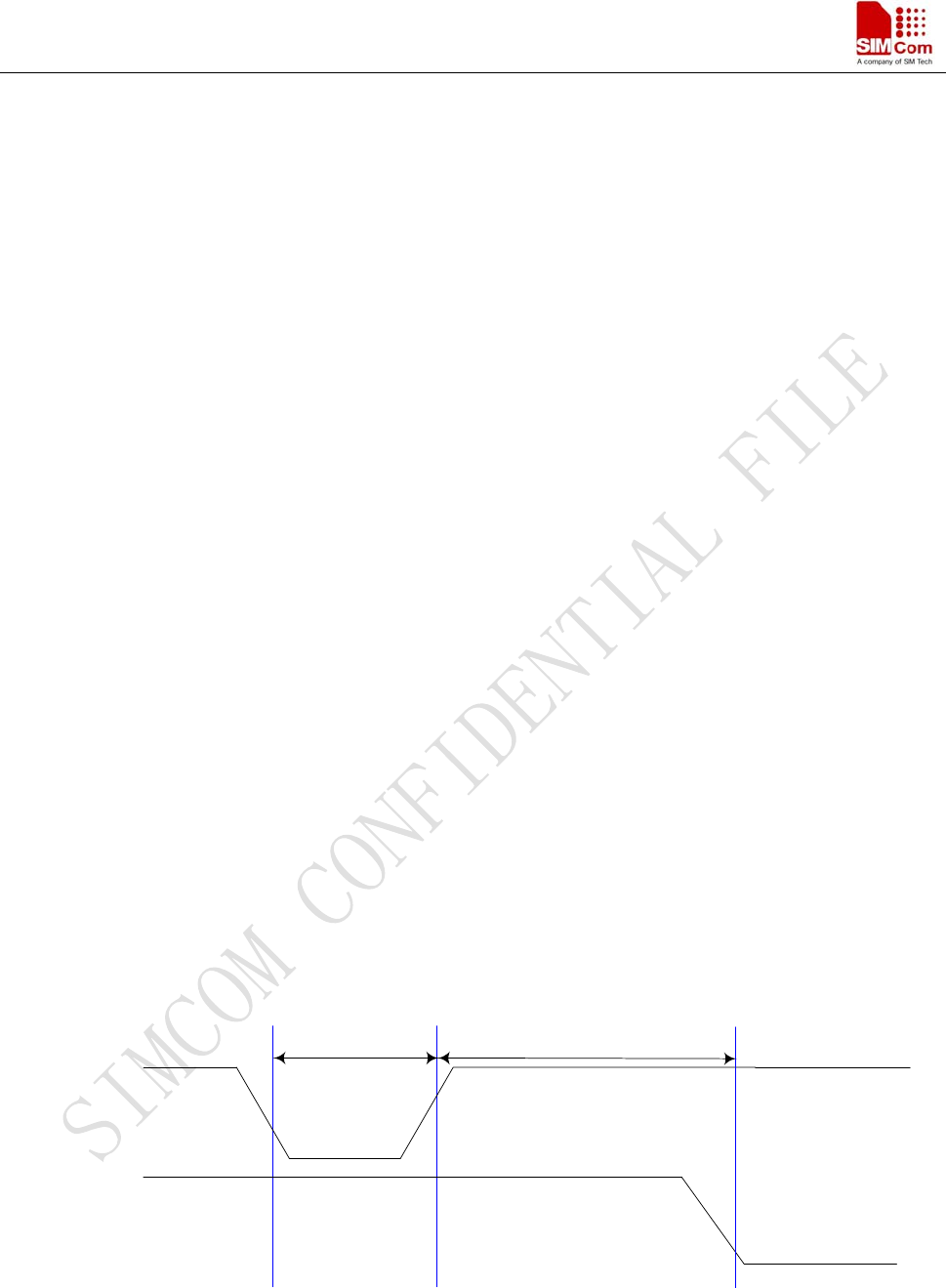
The SIM900B can be turned off by driving the PWRKEY to a low level voltage for a short time and then release.
Please refer to the turn on circuit. The power down scenario illustrates as following figure.
This procedure lets the module log off from the network and allows the software to enter into a secure state and
save data before completely disconnecting the power supply.
Before the completion of the switching off procedure the module will send out result code:
NORMAL POWER DOWN
After this moment, the AT commands can’t be executed. The module enters the POWER DOWN mode, only the
RTC is still active. POWER DOWN can also be indicated by VDD_EXT pin, which is a low level voltage in this
mode.
VDD_EXT
(OUTPUT)
VIL<0.9V
VIH > 2.55V
Pulldown >1s
PWRKEY
(INPUT)
VOL < 0.1V
Delay > 1.7s
Logout net
Figure 9: Timing of turn off system using PWRKEY
SIM900B_HD_V1.03 24.06.2010
26

SIM900B Hardware Design
3.4.2.2 Turn Off SIM900B Using AT Command
AT command “AT+CPOWD=1”can be use to turn off the module. This command lets the module log off from
the network and allows the module to enter into a secure state and save data before completely disconnecting the
power supply.
Before the completion of the switching off procedure the module will send out result code:
NORMAL POWER DOWN
After this moment, the AT commands can’t be executed. The module enters the POWER DOWN mode, only the
RTC is still active. POWER DOWN can also be indicated by VDD_EXT pin, which is a low level voltage in this
mode.
Please refer to document [1] for detail about the AT command of “AT+CPOWD”.
3.4.2.3 Over-voltage or Under-voltage Automatic Shutdown
The module will constantly monitor the voltage applied on the VBAT. If the voltage ≤ 3.2V, the following URC
will be presented:
UNDER-VOLTAGE WARNNING
If the voltage ≥ 4.7V, the following URC will be presented:
OVER-VOLTAGE WARNNING
The uncritical voltage range is 3.1V to 4.8V. If the voltage > 4.8V or < 3.1V, the module will be automatic
shutdown soon.
If the voltage < 3.1V, the following URC will be presented:
UNDER-VOLTAGE POWER DOWN
If the voltage > 4.8V, the following URC will be presented:
OVER-VOLTAGE POWER DOWN
After this moment, no further more AT commands can be executed. The module logs off from network and enters
POWER DOWN mode, and only the RTC is still active. POWER DOWN can also be indicated by VDD_EXT
pin, which is a low level voltage in this mode.
3.4.2.4 Over-temperature or Under-temperature Automatic Shutdown
The module will constantly monitor the temperature of the module, if the temperature > +80 , the following ℃
URC will be presented:
+CMTE:1
If the temperature < -30 , the following URC will be presented:℃
+CMTE:-1
The uncritical temperature range is -40 to ℃+85 . If the temperature ℃> +85 or ℃< -40 , the module will be ℃
automatic shutdown soon.
If the temperature >+ 85 , the following URC will be presented℃:
+CMTE:2
If the temperature < -40℃, the following URC will be presented:
+CMTE:-2
After this moment, the AT commands can’t be executed. The module logs off from network and enters POWER
SIM900B_HD_V1.03 24.06.2010
27
SIM900B Hardware Design
DOWN mode, and only the RTC is still active. POWER DOWN can also be indicated by VDD_EXT pin, which
is a low level voltage in this mode.
To monitor the temperature, the “AT+CMTE” command can be used to read the temperature when the module is
power on.
For details please refer to document [1]
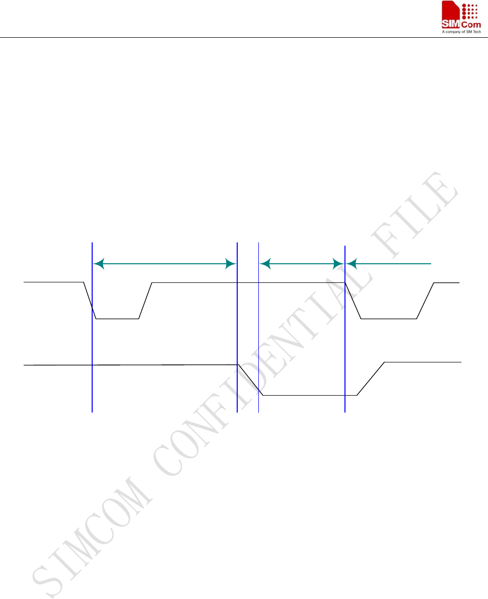
3.4.3 Restart SIM900B Using the PWRKEY Pin
By driving the PWRKEY to a low level voltage for a short time and then release ,SIM900B can be restarted, the
timing is the same as turning on SIM900B using the PWRKEY pin. Before restarting the SIM900B, you need
delay at least 500ms from detecting the VDD_EXT low level on. The restarting scenario illustrates as the
following figure.
VDD_EXT
(OUTPUT)
H
PWRKEY
(INPUT)
Delay > 500ms
Turn off
Pull down the PWRKEY
to turn on the module
Restart
Figure 10: Timing of restart system
3.5 Power Saving
There are two methods for the module to enter into low current consumption status. “AT+CFUN” is used to set
module into minimum functionality mode and DTR signal can be used to control system enter or exit SLEEP
mode (or slow clocking mode).
3.5.1 Minimum Functionality Mode
Minimum functionality mode reduces the functionality of the module to a minimum and, thus, minimizes the
current consumption to the lowest level. This mode is set with the “AT+CFUN” command which provides the
choice of the functionality levels <fun>=0,1,4
z 0: minimum functionality;
z 1: full functionality (default);
z 4: disable phone both transmit and receive RF circuits;
SIM900B_HD_V1.03 24.06.2010
28

SIM900B Hardware Design
If SIM900B has been set to minimum functionality by “AT+CFUN=0”, the RF function and SIM card function
will be closed. In this case, the serial port is still accessible, but all AT commands correlative with RF function or
SIM card function will not be accessible.
If SIM900B has been set by “AT+CFUN=4”, the RF function will be closed, the serial port is still active. In this
case all AT commands correlative with RF function will not be accessible.
After SIM900B has been set by “AT+CFUN=0” or “AT+CFUN=4”, it can return to full functionality by
“AT+CFUN=1”.
For detailed information about “AT+CFUN”, please refer to document [1].
3.5.2 Sleep Mode (Slow Clock Mode)
DTR signal can be used to control SIM900B module to enter or exit the SLEEP mode in customer applications
When DTR is in high level and there is no on air and hardware interrupt (such as GPIO interrupt or data on serial
port), SIM900B will enter SLEEP mode automatically. In this mode, SIM900B can still receive paging or SMS
from network but the serial port is not accessible.
Note: For SIM900B, it requests to set AT command “AT+CSCLK=1” to enable the sleep mode; the default
value is 0, that can’t make the module enter sleep mode. For more details please refer to our AT command list.
3.5.3 Wake Up SIM900B from SLEEP Mode
When SIM900B is in SLEEP mode, the following methods can wake up the module.
z Enable DTR pin to wake up SIM900B.
If DTR pin is pulled down to a low level,this signal will wake up SIM900B from power saving mode. The
serial port will be active after DTR changed to low level for about 50ms.
z Receiving a voice or data call from network to wake up SIM900B.
z Receiving a SMS from network to wake up SIM900B.
3.6 Summary of State Transitions (except SLEEP mode)
The following figure shows how to proceed from one mode to another.
Normal Mode
Normal Mode Power Down
Mode
Power Down
Mode
AT+CPOWD or Drive
PWRKEY to ground
Drive PWRKEY to ground
Figure 11: State Transition
SIM900B_HD_V1.03 24.06.2010
29
SIM900B Hardware Design
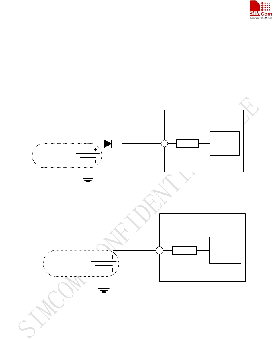
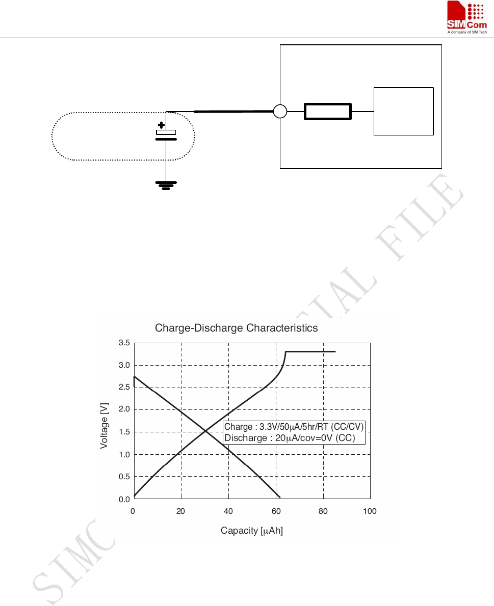
3.7 RTC Backup
The RTC (Real Time Clock) power supply of module can be provided by an external capacitor or a battery
(rechargeable or non-chargeable) through the VRTC.
Note: If the RTC function is enabled, a battery or capacitor should be connected with the VRTC pin. If this
function is not needed, a 4.7uF capacitor is recommended to connect to the VRTC pin.
The following figures show various sample circuits for RTC backup.
RTC
Core
10K
SIM900B
VRTC
Non-chargeable
Backup Battery
Figure 12: RTC supply from non-chargeable battery
RTC
Core
10K
SIM900B
VRTC
Rechargeable
Backup Battery
Figure 13: RTC supply from rechargeable battery
SIM900B_HD_V1.03 24.06.2010
30
SIM900B Hardware Design
RTC
Core
10K
SIM900B
VRTC
Large-capacitance
Capacitor
Figure 14: RTC supply from capacitor
z Li-battery backup
Coin-type Rechargeable Capacitor such as XH414H-IV01E form Seiko can be used.
Typical charge curves for each cell type are shown in following figures. Note that the rechargeable Lithium type
coin cells generally come pre-charged from the vendor.
Figure 15: Seiko XH414H-IV01E Charge Characteristic
3.8 Serial Interfaces
Table 7: Pin definition of the serial interfaces
SIM900B_HD_V1.03 24.06.2010
31
SIM900B Hardware Design
Name Pin Function
DCD 28 Data carrier detection
DTR 38 Data terminal ready
RXD 40 Receive data
TXD 42 Transmit data
RTS 44 Request to send
CTS 46 Clear to send
Serial port
RI 48 Ring indicator
DBG_RXD 47 Receive data
Debug port
DBG_TXD 49 Transmit data
SIM900B provides two unbalanced asynchronous serial ports. One is the serial port and the other is the debug port.
The GSM module is designed as a DCE (Data Communication Equipment), following the traditional DCE-DTE
(Data Terminal Equipment) connection. The module and the client (DTE) are connected through the following
signal (as following figure shows). Autobauding supports baud rate from 1200bps to 57600bps.
Serial port
z TXD: Send data to the RXD signal line of the DTE
z RXD: Receive data from the TXD signal line of the DTE
Debug port
z DBG_TXD: Send data to the RXD signal line of the DTE
z DBG_RXD: Receive data from the TXD signal line of the DTE
The logic levels are described in following table.
Table 8: Logic levels of the serial port and debug port
Parameter Min Max Unit
VIL 0 0.15*VDD_EXT V
VIH 0.85 *VDD_EXT VDD_EXT V
VOL 0 0.1 V
VOH VDD_EXT -0.1 VDD_EXT V
SIM900B_HD_V1.03 24.06.2010
32
SIM900B Hardware Design
TXD
RXD
RTS
CTS
DTR
DCD
RI
TXD
RXD
RTS
CTS
DTR
DCD
RING
MODULE (DCE) CUSTOMER (DTE)
Serial port1Serial port
Debug port Serial port2
DBG_RX
DBG_TX TXD
RXD
Figure 16: Connection of the serial interfaces
3.8.1 Function of serial port & debug port supporting
Serial port
z Modem device.
z Contains data lines TXD and RXD, State lines RTS and CTS, Control lines DTR, DCD and RI.
z Serial port can be used for CSD FAX, GPRS service and send AT command of controlling module. Also
serial port can be used for multiplexing function. SIM900B supports only basic mode of multiplexing so far.
z Serial port supports the communication rates as following:
1200, 2400, 4800, 9600, 19200, 38400, 57600 and 115200bps.
z Autobauding supports baud rates as following:
1200, 2400, 4800, 9600, 19200, 38400, and 57600bps,the default setting is autobauding。
Autobauding allows the GSM engine to automatically detect the baud rate configured in the host application. The
serial port of the GSM engine supports autobauding for the following baud rates: 1200, 2400, 4800, 9600, 19200,
38400, 57600bps. Factory setting is autobauding enabled. This gives you the flexibility to put the GSM engine
into operation no matter what baud rate your host application is configured to. To take advantage of autobauding
mode, specific attention should be paid to the following requirements:
Synchronization between DTE and DCE:
When DCE powers on with the autobauding enabled, user must first send “A” to synchronize the baud rate. It is
recommended to wait 2 to 3 seconds before sending “AT” character. After receiving the “OK” response, DTE
and DCE are correctly synchronized. The more information please refer to the AT command “AT+IPR”.
Restrictions on autobauding operation
SIM900B_HD_V1.03 24.06.2010
33
SIM900B Hardware Design
z The serial port has to be operated at 8 data bits, no parity and 1 stop bit (factory setting).
z The Unsolicited Result Codes like "RDY", "+CFUN: 1" and "+CPIN: READY” are not indicated when you
start up the ME while autobauding is enabled. This is due to the fact that the new baud rate is not detected
unless DTE and DCE are correctly synchronized as described above.
Note: use “AT+IPR=x “to set a fixed baud rate and save the configuration to non-volatile flash memory. After
the configuration is saved as fixed baud rate, the Unsolicited Result Codes like "RDY" should be received
from the serial port all the time that the SIM900B is power on.
Debug port
z Null modem port
z Only contain Data lines TXD and RXD
z Debug Port used for debugging and upgrading firmware. It cannot be used for CSD call, FAX call. And the
Debug port can not use multiplexing function. It does not support autobauding function.
z Debug port supports the communication rates is 115200bps
3.8.2 Software Upgrade and Software Debug
The DBG_TXD, DBG_RXD and GND must be connected to the IO connector when user need to upgrade
software and debug software, the DBG_TXD, DBG_RXD should be used for software upgrade and for software
debugging. The TXD and RXD also should be connected to the IO connector, if user wants to send AT command
or data stream to SIM900B. The PWRKEY pin is recommended to connect to the IO connector. The user also
can add a switch between the PWRKEY and the GND. The PWRKEY should be connected to the GND when
SIM900B is upgrading software. Please refer to the following figure.
MODULE(DCE)
DBG_TXD
DBG_RXD
GND
PWRKEY
TXD
RXD
GND
PWRKEY
Serial port I/O Connector
Figure 17: Connection of software upgrade and software debug
The serial port and the debug port don’t support the RS_232 level and it only supports the CMOS level. Please
refer to the table 10 for details about the voltage level. You should add the level converter IC between the DCE
and DTE, if you connect it to the computer. Please refer to the following figure
SIM900B_HD_V1.03 24.06.2010
34
SIM900B Hardware Design
Figure 18: RS232 level converter circuit
3.9 Audio Interfaces
Table 9: Pin define of the Audio interface
Name Pin Function
MIC1P 53 Microphone1 input +
MIC1N 55 Microphone1 input -
SPK1P 54 Audio1 output+
(AIN1/AOUT1)
SPK1N 56 Audio1 output-
MIC2P 57 Microphone2 input +
MIC2N 59 Microphone2 input -
SPK2P 58 Audio2 output+
(AIN2/AOUT2)
SPK2N 60 Audio2 output-
The module provides two analogy input channels, AIN1 and AIN2, which may be used for both microphone and
line inputs. The electret microphone is recommended when the interface is used for microphone. One of the two
channels is typically used with a microphone built into a handset. The other channel is typically used with an
external microphone or external line input. The module analogy input configuration is determined by control
register settings and established using analogy multiplexes.
For each channels, “AT+CMIC” can be used to adjust the input gain level of microphone, “AT+SIDET” can be
SIM900B_HD_V1.03 24.06.2010
35
SIM900B Hardware Design
used to set the side-tone level. In addition, “AT+CLVL” can be used to adjust the output gain level of both
receiver and speaker at the same time, use AT+CHFA to activate one of the two audio channels and deactivate the
other one.. For more details, please refer to document [1].
Note: Use AT command AT+CHFA to select_audio channel:
0— AIN1/AOUT1 (normal audio channel), the default value is 0.
1— AIN2/AOUT2(aux_audio channel) .
It is suggested that you adopt one of the following two matching circuits in order to improve audio performance.
The difference audio signals have to be layout according to difference signal layout rules. As show in following
figures (Note: all components package are 0603.) If an amplifier circuit for audio is needed, then National
company’s LM4890 is recommended. Of course it can select it according to your requirement.
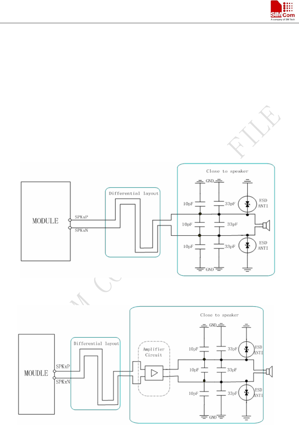
3.9.1 Speaker Interface Configuration
Figure 19: Speaker interface configuration
Figure 20: Speaker interface with amplifier configuration
SIM900B_HD_V1.03 24.06.2010
36
SIM900B Hardware Design
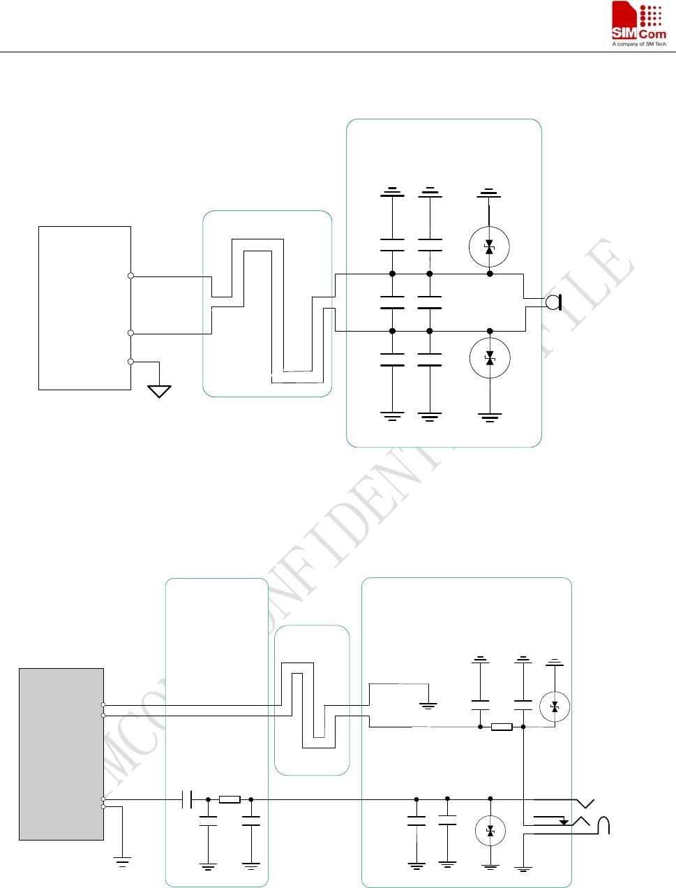
3.9.2 Microphone Interfaces Configuration
10pF 33pF
33pF
33pF
Close to Microphone
MICxP
MICxN
GND
GND
Differential layout
AGND
MODULE
Electret
Microphone
GND
GND
10pF
10pF
GND
GND
ESD
ANTI
ESD
ANTI
AGND
Figure 21: Microphone interface configuration
3.9.3 Earphone Interface Configuration
1
2
4
3
Amphenol
SPK2P
MIC2N
MIC2P
1uF
10R
100R
33pF
GND
GNDGND
GND
Close to MODULE
Close to Socket
Differential
layout
33pF 33pF
33pF
33pF 10pF
GND GND
GND
GND
MODULE
GND
GND
SPK2N
GND
Figure 22: Earphone interface configuration
SIM900B_HD_V1.03 24.06.2010
37
SIM900B Hardware Design
3.9.4 Referenced Electronic Characteristic
Table 10: MIC Input Characteristics
Parameter Min Typ Max Unit
Working Voltage 1.2 1.5 2.0 V
Working Current 200 500 uA
External Microphone Load Resistance 1.2 2.2 k Ohms
Internal biasing DC Characteristics 2.5 V
THD <1% at
F=1KHz; pre-amp
gain = 20 dB;
PGA gain = 14 dB
15.9 mVrms Differential input
voltage
THD <5% at
F=1KHz;pre-amp
gain = 0 dB; PGA
gain = 0 dB
740 mVrms
Table 11: Audio Output Characteristics
Parameter Conditions Min Typ Max Unit
load Resistance 27 32 - Ohm
Biasing voltage 1.4 V
Output swing
Voltage(single) 1.1V Vpp
Output swing
Voltage(differentia
l)
2.2 Vpp
RL=32 Ohm
THD=0.1% - 91 - mW
Normal
Output(SPK1P/1N
)
RL=32 Ohm
THD=1% - 96 - mW
load Resistance 27 32 - Ohm
Biasing voltage 1.4 V
Normal
Output(SPK2P/2N
)
Output swing
Voltage(single) 1.1V V
SIM900B_HD_V1.03 24.06.2010
38
SIM900B Hardware Design
Output swing
Voltage(differentia
l)
2.2 V
RL=32 Ohm
THD=0.1% - 91 - mW
RL=32 Ohm
THD=1% - 96 - mW
3.10 Buzzer
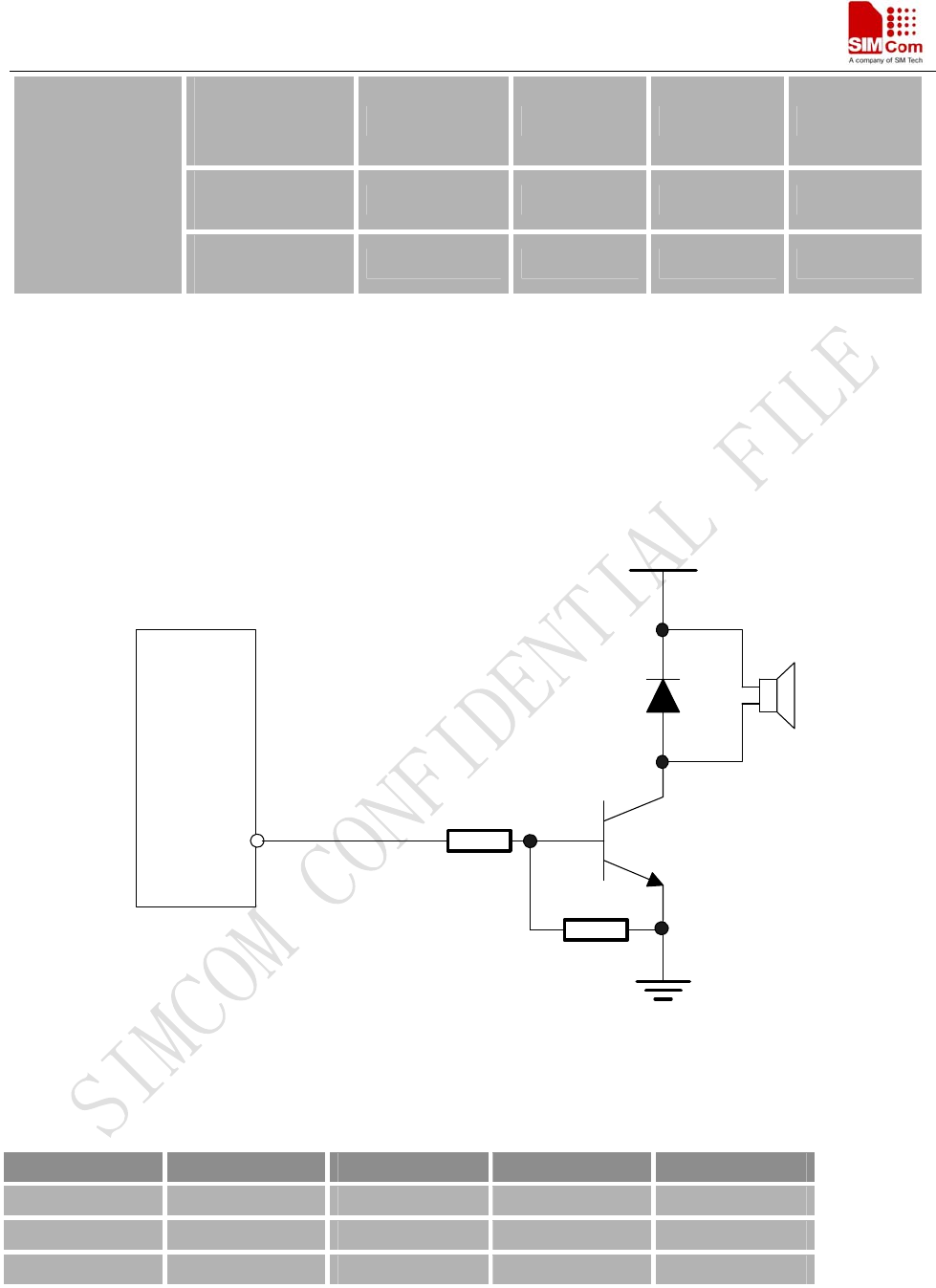
The BUZZER on the board-to-board connector can be used to drive a buzzer to indicate incoming call. The
output volume of buzzer can be set by “AT+CRSL”. The reference circuit for buzzer shown as following figure:
MODULE
4.7K
47K
VBAT
BUZZER
Figure 23: Reference circuit of Buzzer
Table 12: Buzzer Output Characteristics
Parameter Min Typ Max Unit
Working Voltage 2.4 2.85 3.0 V
Working Current 2 mA
Load Resistance 1 k Ohms
SIM900B_HD_V1.03 24.06.2010
39
SIM900B Hardware Design
3.11 SIM Card Interface
3.11.1 SIM Card Application
The user can use AT Command to get information in SIM card. For more information, please refer to document
[1].
The SIM interface supports the functionality of the GSM Phase 1 specification and also supports the functionality
of the new GSM Phase 2+ specification for FAST 64 kbps SIM (intended for use with a SIM application
Tool-kit).
Both 1.8V and 3.0V SIM Cards are supported.
The SIM interface is powered from an internal regulator in the module having normal voltage 3V. All pins reset
as outputs driving low. Logic levels are as described in table
Table 13: Pin define of the SIM interface
Name Pin Function
SIM_VDD 19 SIM Card Power output automatic output on SIM mode,
one is 3.0V±10%, another is 1.8V±10%. Current is about
10mA.
SIM_DATA 21 SIM Card data I/O
SIM_CLK 23 SIM Card Clock
SIM_RST 25 SIM Card Reset
SIM_PRESENCE 16 SIM Card Presence
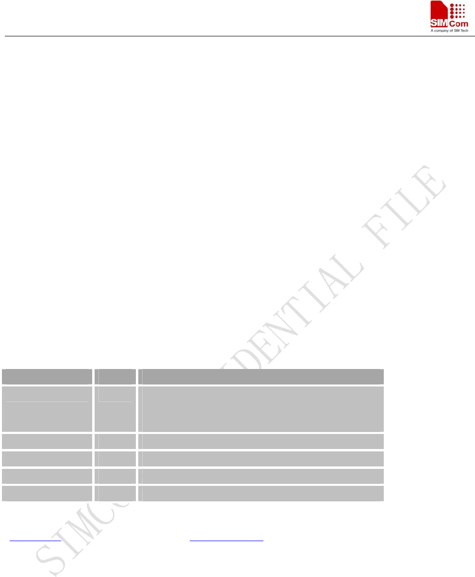
Following is the reference circuit about SIM interface. We recommend an Electro-Static discharge device ST
(www.st.com ) ESDA6V1W5 or ON SEMI (www.onsemi.com ) SMF05C for “ESD ANTI”. The 22Ω resistors
showed in the following figure should be added in series on the IO line between the module and the SIM card for
protecting the SIM I/O port. The pull up resistor (about 15KΩ) on the SIM_DATA line already added in the
module. Note that the SIM peripheral circuit should be close to the SIM card socket.
The SIM_PRESENCE pin is used for detecting the SIM card insert or removal. The user can use the AT
command “AT+CSDT” to set the SIMCARD configuration. For detail of this AT command, please refer to
document [1]:
8 pins SIM card holder can be selected . The reference circuit about 8 pins SIM card holder illustrates as
following figure.
SIM900B_HD_V1.03 24.06.2010
40
SIM900B Hardware Design
MODULE
SMF05C
SIM_VDD
SIM_CLK
SIM_DATA
SIM_RST
SIM_PRESENCE
VCC GND
RST VPP
CLK I/O
PRESENCE GND
22R
22R
22R
220nF MOLEX-91228
SIM
CARD
22pF
Figure 24: Reference circuit of the 8 pins SIM card
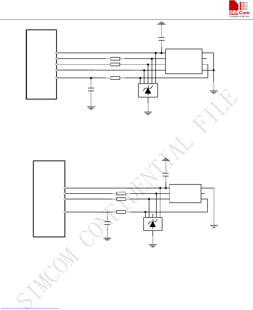
If the SIM card detection function don’t use, the SIM_PRESENCE pin can be keep open. The reference circuit
about 6 pins SIM card illustrates as following figure.
MODULE
SMF05C
SIM_VDD
SIM_CLK
SIM_DATA
SIM_RST
22pF
VCC GND
RST VPP
CLK I/O
22R
22R
22R
220nF
C707 10M006 512 2
SIM
CARD
Figure 25: Reference circuit of the 6 pins SIM card
3.11.2 Design Considerations for SIM Card Holder
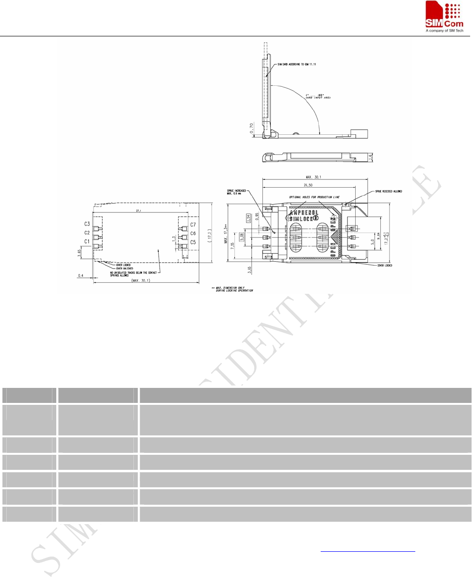
For 6 pins SIM card holder, we recommend to use Amphenol C707 10M006 512 2, the user can visit
http://www.amphenol.com for more information about the holder.
SIM900B_HD_V1.03 24.06.2010
41
SIM900B Hardware Design
Figure 26: Amphenol C707 10M006 512 2 SIM card holder
Table 14: Pin description (Amphenol SIM card holder)
Pin Name Signal Description
C1 SIM_VDD SIM Card Power supply, it can identify automatically the SIM Card power
mode,one is 3.0V±10%, another is 1.8V±10%. Current is about 10mA.
C2 SIM_RST SIM Card Reset.
C3 SIM_CLK SIM Card Clock.
C5 GND Connect to GND.
C6 VPP Not connect.
C7 SIM_DATA SIM Card data I/O.
For 8 pins SIM card holder, Molex 91228 is recommended. The user can visit http://www.molex.com for more
information about the holder.
SIM900B_HD_V1.03 24.06.2010
42
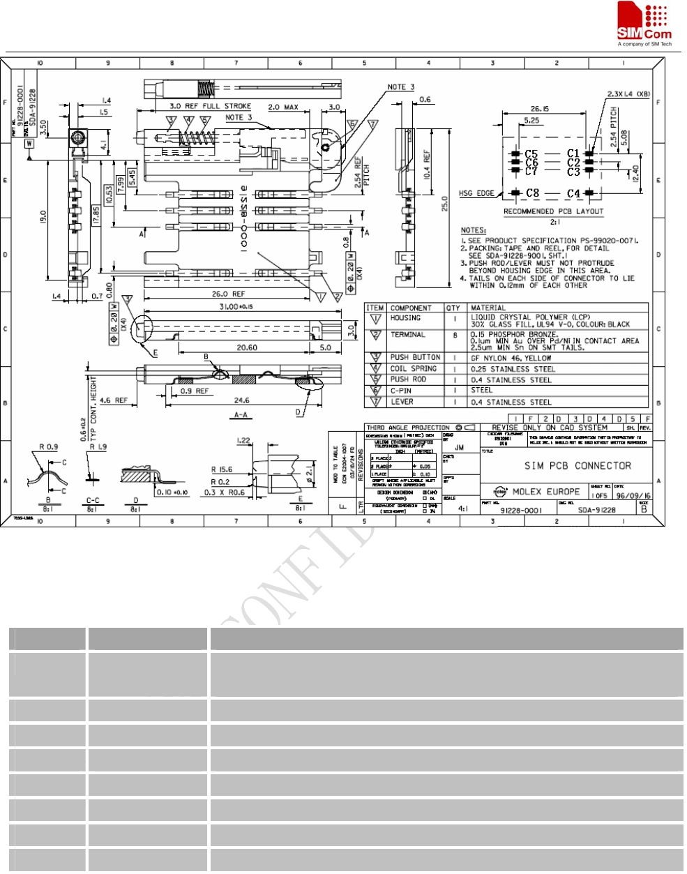
SIM900B Hardware Design
SIM900B_HD_V1.03 24.06.2010
43
Figure 27: Molex 91228 SIM card holder
Table 15: Pin description (Molex SIM card holder)
Pin Name Signal Description
C1 SIM_VDD SIM Card Power supply, it can identify automatically the SIM Card power
mode,one is 3.0V±10%, another is 1.8V±10%. Current is about 10mA.
C2 SIM_RST SIM Card Reset
C3 SIM_CLK SIM Card Clock
C4 GND Connect to GND
C5 GND Connect to GND
C6 VPP Not connect
C7 SIM_DATA SIM Card data I/O
C8 SIM_PRESENCE Detect SIM Card Presence
NOTE: the sim900B can support embedded SIM IC or embedded SIM card holder, but these functions
aren’t included in the default version, please contact SIMCom for more details.
SIM900B Hardware Design
3.12 LCD Display Interface
SIM900B provides a serial LCD display interface that supports serial communication with LCD device.
When used as LCD interface, the following table is the pin definition. LCD interface timing should be united
with the LCD device.
Table 16: Pin define of the LCD interface
Name Pin Function
DISP_DATA 18 Display data output
DISP_CLK 20 Display clock for LCD
DISP_CS 22 Display enable
DISP_D/C 24 Display data or command select
DISP_RST 26 LCD reset
Note: This function is not supported in the default firmware. There must be some customized firmware if you
want. Please contact SIMCom for more details.
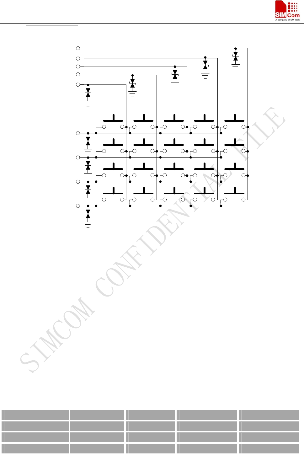
3.13 Keypad Interface
The keypad interface consists of 5 keypad column outputs and 4 keypad row inputs. The basic configuration is 5
keypad columns and 4 keypad rows, giving 20 keys.
Table 17: Pin define of the keypad interface
Name Pin Function
KBC0 27
GPIO4/KBC1 29
GPIO3/KBC2 31
GPIO2/KBC3 33
GPIO1/KBC4 35
Keypad matrix column
GPIO9/KBR1 39
GPIO8/KBR2 41
GPIO7/KBR3 43
GPIO6/KBR4 45
Keypad matrix row
The keypad interface allows a direct external matrix connection. A typical recommended circuit about the keypad
is as shown in the following figure.
SIM900B_HD_V1.03 24.06.2010
44
SIM900B Hardware Design
KBR4
KBR3
KBR2
KBR1
KBC0
KBC1
KBC2
KBC3
KBC4
GND
MODULE
Figure 28: Reference circuit of the keypad interface
*Note:
1. This function is not supported in the default firmware. There must be customized firmware if you want.
Please contact SIMCom for more details.
2.KBR0&KBC0 is used to power off the module, so do not connect them for other application.
3. keypad is the second function of this pin , the default function is GPIO.
3.14 ADC
SIM900B provides one auxiliary ADC (General purpose analog to digital converter.) as voltage input pin, which
can be used to detect the values of some external items such as voltage, temperature etc. We can use AT
command “AT+CADC” to read the voltage value on ADC. For detail of this AT command, please refer to
document [1].
Table 18: ADC specification
MIN Type MAX Units
Voltage range 0 - 2.8 V
ADC Resolution - 10 - bits
Sampling rate - - 200K Hz
SIM900B_HD_V1.03 24.06.2010
45
SIM900B Hardware Design
3.15 Behaviors of the RI
Table 19: Behaviours of the RI
State RI respond
Standby
HIGH
Voice calling Change LOW, then:
(1)Change to HIGH when establish calling.
(2)Use AT command ATH, the RI pin changes to HIGH.
(3)Sender hangs up, change to HIGH.
Data calling Change LOW, then:
(1)Change to HIGH when establish calling.
(2)Use AT command ATH, the RI changes to HIGH.
SMS When receive SMS, The RI will change to LOW and hold low level about 120 ms, then
change to HIGH.
URC Some URCs triggers 120ms low level on RI. For more details, please refer to document [10]
If the module is used as caller, the RI will maintain high. However, when it is used as receiver, following is timing
of ring.
Power on Ring MO or MT
Hang up
Ring Hang on
(talking)
MO or
MT
Hang up
Ring
RI
HIGH
LOW
Figure 29: SIM900B Services as Receiver
RI
Power on calling Hang up Echo talking calling Echo Hang up
HIGH
LOW
Figure 30: SIM900B Services as caller
3.16 Network Status Indication
The NETLIGHT can be used to drive a network status indication LED lamp. The working state of this pin is
listed in following table:
SIM900B_HD_V1.03 24.06.2010
46
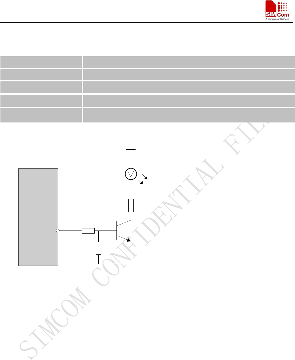
SIM900B Hardware Design
Table 20: Working state of the NETLIGHT
State SIM900B function
Off SIM900B is not running
64ms On/ 800ms Off SIM900B does not find the network
64ms On/ 3000ms Off SIM900B find the network
64ms On/ 300ms Off GPRS communication
The reference circuit is shown as the following figure:
300R
4.7K
47K
MODULE
NETLIGHT
VBAT
Figure 31: Reference circuit of NETLIGHT
SIM900B_HD_V1.03 24.06.2010
47
SIM900B Hardware Design
3.17 General Purpose Input Output (GPIO)
SIM900B provides a limited number of General Purpose Input/Output signal pin.
Name Pin Function RESET
GPIO0 32 Input pull down
GPIO1/KBC4 35 Input pull down
GPIO2/KBC3 33 Input pull down
GPIO3/KBC2 31 Input pull down
GPIO4/KBC1 29 Input pull down
GPIO6/KBR4 45 Input pull down
GPIO7/KBR3 43 Input pull down
GPIO8/KBR2 41 Input pull down
GPIO9/KBR1 39
General Purpose Input/Output Port
Input pull down
Table 21: Pin define of the GPIO interface
Note: This function is not supported in the default firmware. There must be special firmware if you require.
Please contact SIMCom for more details .
SIM900B_HD_V1.03 24.06.2010
48
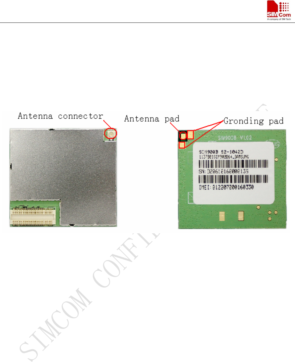
SIM900B Hardware Design
4 Antenna Interface
The RF interface has an impedance of 50Ω. To suit the physical design of individual applications, SIM900B
offers alternatives:
z Recommended approach: antenna connector on the component side of the PCB
z Antenna pad and grounding plane placed on the bottom side.
Figure 32 : The RF interface of module
The antenna can be soldered to the pad, or attached via contact springs. To help you to ground the antenna,
SIM900B comes with a grounding plane located close to the antenna pad.
SIM900B material properties:
SIM900B PCB Material: FR4
Antenna pad: Gold plated pad
To minimize the loss on the RF cable, it need be very careful to choose RF cable. We recommend the insertion
loss should be meet following requirements:
z GSM900<1dB
z DCS1800/PCS1900<1.5dB
SIM900B_HD_V1.03 24.06.2010
49
SIM900B Hardware Design
4.1 Module RF Output Power
Table 22: SIM900B conducted RF output power
Frequency Max Min
GSM850 33dBm ±2db 5dBm±5db
EGSM900 33dBm ±2db 5dBm±5db
DCS1800 30dBm ±2db 0dBm±5db
PCS1900 30dBm ±2db 0dBm±5db
4.2 Module RF Receive Sensitivity
Table 23: SIM900B conducted RF receive sensitivity
Frequency Receive sensitivity(Typical) Receive sensitivity(Max)
GSM850 -109dBm -107dBm
EGSM900 -109dBm -107dBm
DCS1800 -109dBm -107dBm
PCS1900 -109dBm -107dBm
4.3 Module Operating Frequencies
Table 24: SIM900B operating frequencies
Frequency Receive Transmit
GSM850 869 ~ 894MHz 824 ~ 849 MHz
EGSM900 925 ~ 960MHz 880 ~ 915MHz
DCS1800 1805 ~ 1880MHz 1710 ~ 1785MHz
PCS1900 1930 ~ 1990MHz 1850 ~ 1910MHz
5 Electrical, Reliability and Radio Characteristics
5.1 Absolute Maximum Ratings
The absolute maximum ratings stated in Table 28 are stress ratings under non-operating conditions. Stresses
beyond any of these limits will cause permanent damage to SIM900B.
SIM900B_HD_V1.03 24.06.2010
50
SIM900B Hardware Design
Table 25: Absolute maximum ratings
Parameter Min Max Unit
VBAT - 5.5 V
Peak current of power supply 0 3.0 A
Voltage at digit pins* -0.3 3.1 V
II* - 10 mA
IO* - 10 mA
*For digital interface pins, such as keypad, GPIO, UART and LCD.
5.2 Operating Temperatures
The operating temperature is listed in following table:
Table 26: SIM900B operating temperature
Parameter Min Typ Max Unit
Ambient temperature -30 +25 +80 ℃
Restricted operation* -40 to -30 +80 to +85 ℃
Storage temperature -45 +90 ℃
* The SIM900B does work, but deviations from the GSM specification may occur.
5.3 Power Supply Ratings
Table 27: SIM900B power supply ratings
Parameter Description Conditions Min Typ Max Unit
Supply voltage Voltage must stay within the min/max
values, including voltage drop, ripple, and
spikes.
3.1 4.0 4.8 V VBAT
Voltage drop
during transmit
burst
Normal condition, power control level for
Pout max
300 mV
SIM900B_HD_V1.03 24.06.2010
51

SIM900B Hardware Design
Voltage ripple Normal condition, power control level for
Pout max
@ f<200kHz
@ f>200kHz
50
2
mV
POWER DOWN mode
SLEEP mode(BS-PA-MFRMS=2 )
(BS-PA-MFRMS=5 )
(BS-PA-MFRMS=9 )
50
1.5
1.2
1.0
uA
mA
mA
mA
IDLE mode
GSM 850
EGSM 900
DCS1800
PCS1900
22
22
22
22
mA
TALK mode
GSM 850
EGSM 900
DCS1800
PCS1900
235
247
181
170
mA
DATA mode, GPRS (3 Rx,2Tx)
GSM 850
EGSM 900
DCS1800
PCS1900
436
463
322
303
mA
IVBAT
Average supply
current
DATA mode, GPRS (4 Rx,1Tx)
GSM 850
EGSM 900
DCS1800
PCS1900
270
282
215
205
mA
Peak supply
current (during
Tx
burst)
Power control level for Pout max. 2.0 A
5.4 Current Consumption
Please refer to the following table for the values of current consumption.
Table 28: SIM900B current consumption(VBAT=3.8V)
SIM900B_HD_V1.03 24.06.2010
52
SIM900B Hardware Design
Voice Call
GSM 850/EGSM 900 @power level #5 <300mA,Typical 250mA
@power level #12,Typical 110mA
@power level #19,Typical 80mA
DCS 1800/PCS 1900 @power level #0 <200mA,Typical 180mA
@power level #7,Typical 94mA
@power level #15,Typical 76mA
GPRS Data
DATA mode, GPRS ( 1 Rx,1 Tx ) CLASS 8
GSM 850/EGSM 900 @power level #5 <300mA,Typical 235mA
@power level #12,Typical 102mA
@power leve#19,Typical 74mA
DCS 1800/PCS 1900 @power level #0 <200mA,Typical 170mA
@power level #7,Typical 90mA
@power level #15,Typical 70mA
DATA mode, GPRS ( 3 Rx, 2 Tx ) CLASS 10
GSM 850/EGSM 900 @power level #5<450mA,Typical 440mA
@power level #12,Typical 185mA
@power level #19,Typical 125mA
DCS 1800/PCS 1900 @power level #0 <350mA,Typical 320mA
@power level #7,Typical 155mA
@power level #15,Typical 120mA
DATA mode, GPRS ( 4 Rx,1 Tx ) CLASS 8
GSM 850/EGSM 900 @power level #5 <300mA,Typical 273mA
@power level #12,Typical 145mA
@power level #19,Typical 120mA
DCS 1800/PCS 1900 @power level #0<300mA,Typical 205mA
@power level #7,Typical 130mA
@power level #15,Typical 110mA
Class 10 is default set when the module works at data translation mode, the module can also work at class 8 set by
AT command.
5.5 Electro-Static Discharge
The GSM engine is not protected against Electrostatic Discharge (ESD) in general. Therefore, it is subject to ESD
handing precautions that typically apply to ESD sensitive components. Proper ESD handing and packaging
procedures must be applied throughout the processing, handing and operation of any application using a SIM900B
module.
The measured values of SIM900B are shown as the following table:
Table 29: The ESD endure statue measured table (Temperature: 25 , Humidity:45% )℃
SIM900B_HD_V1.03 24.06.2010
53
SIM900B Hardware Design
Part Contact discharge Air discharge
VBAT ±5KV ±10KV
GND ±5KV ±10KV
RXD, TXD ±2KV ±8KV
Antenna port ±5KV ±10KV
SPK_P/N
MIC_P/N ±4KV ±8KV
PWRKEY ±2KV ±8KV
Other port TBD TBD
SIM900B_HD_V1.03 24.06.2010
54
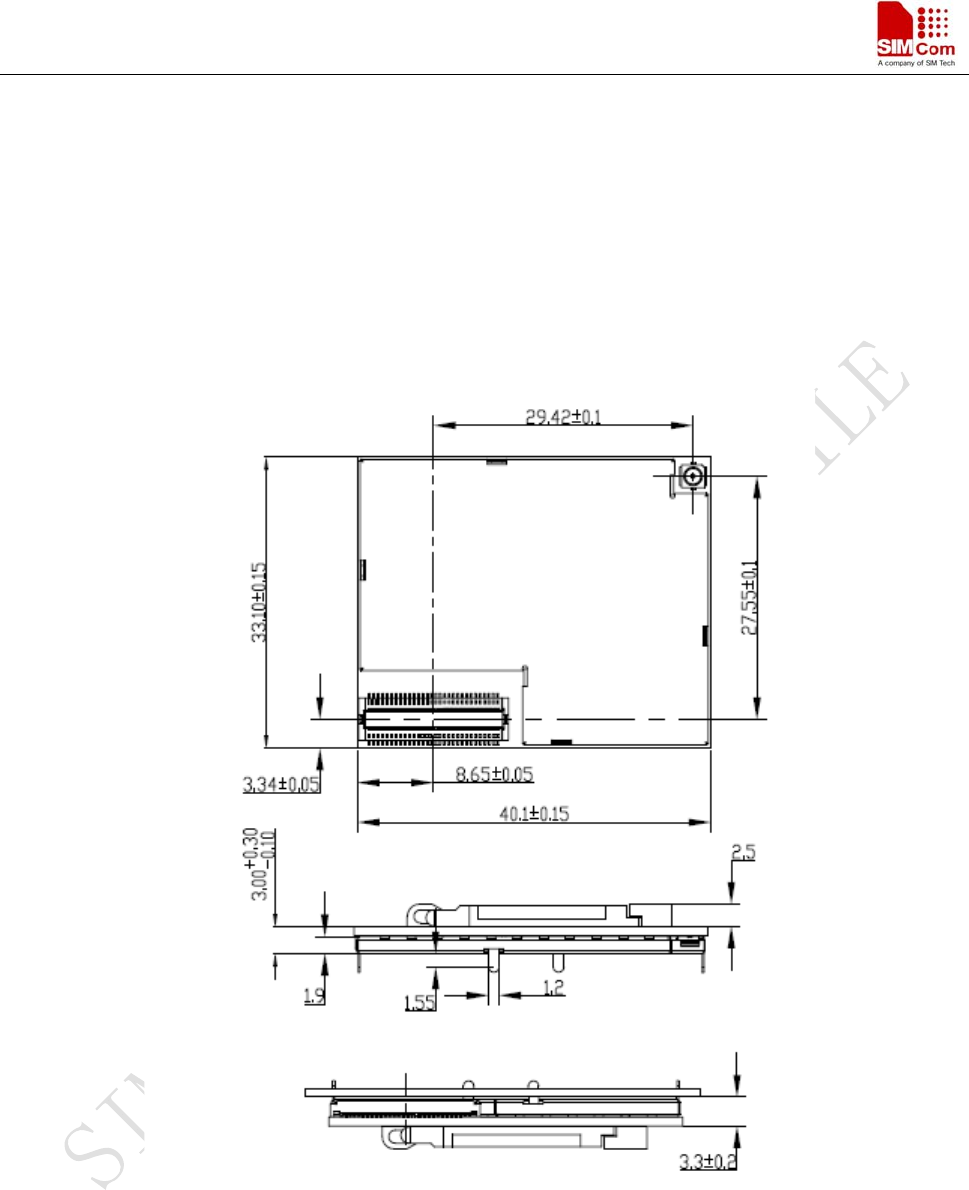
SIM900B Hardware Design
6 Mechanics
This chapter describes the mechanical dimensions of SIM900B.
6.1 Mechanical Dimensions of SIM900B
Following shows the Mechanical dimensions of SIM900B (top view, side view and bottom view).
Figure 33: Top an Side Mechanical dimensions of module (Unit: mm)
SIM900B_HD_V1.03 24.06.2010
55
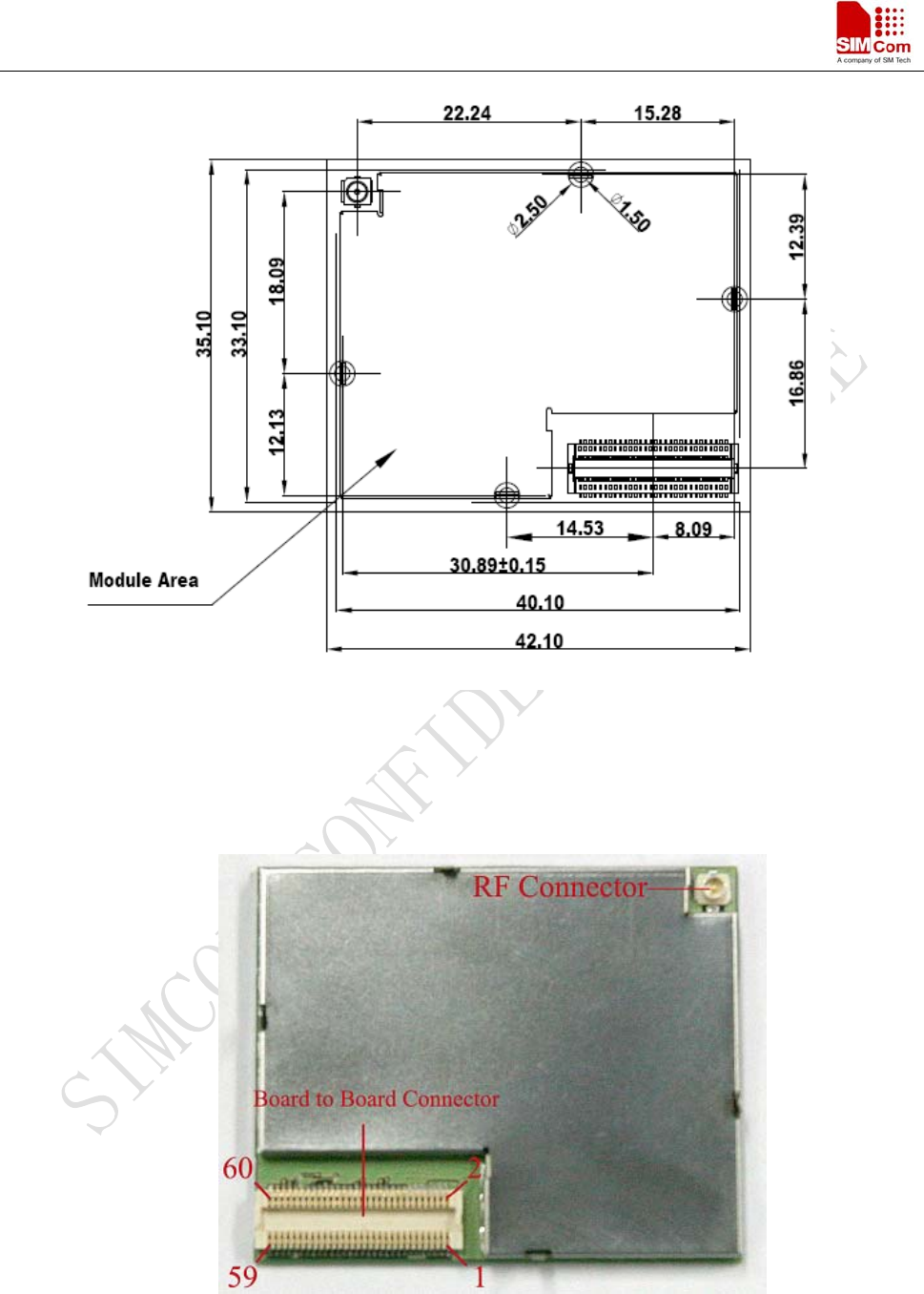
SIM900B Hardware Design
Figure 34:Mechanical dimensions of module PCB decal(Unit: mm)
6.2 Top View of the SIM900B
Figure 35: Top view of the SIM900B
SIM900B_HD_V1.03 24.06.2010
56
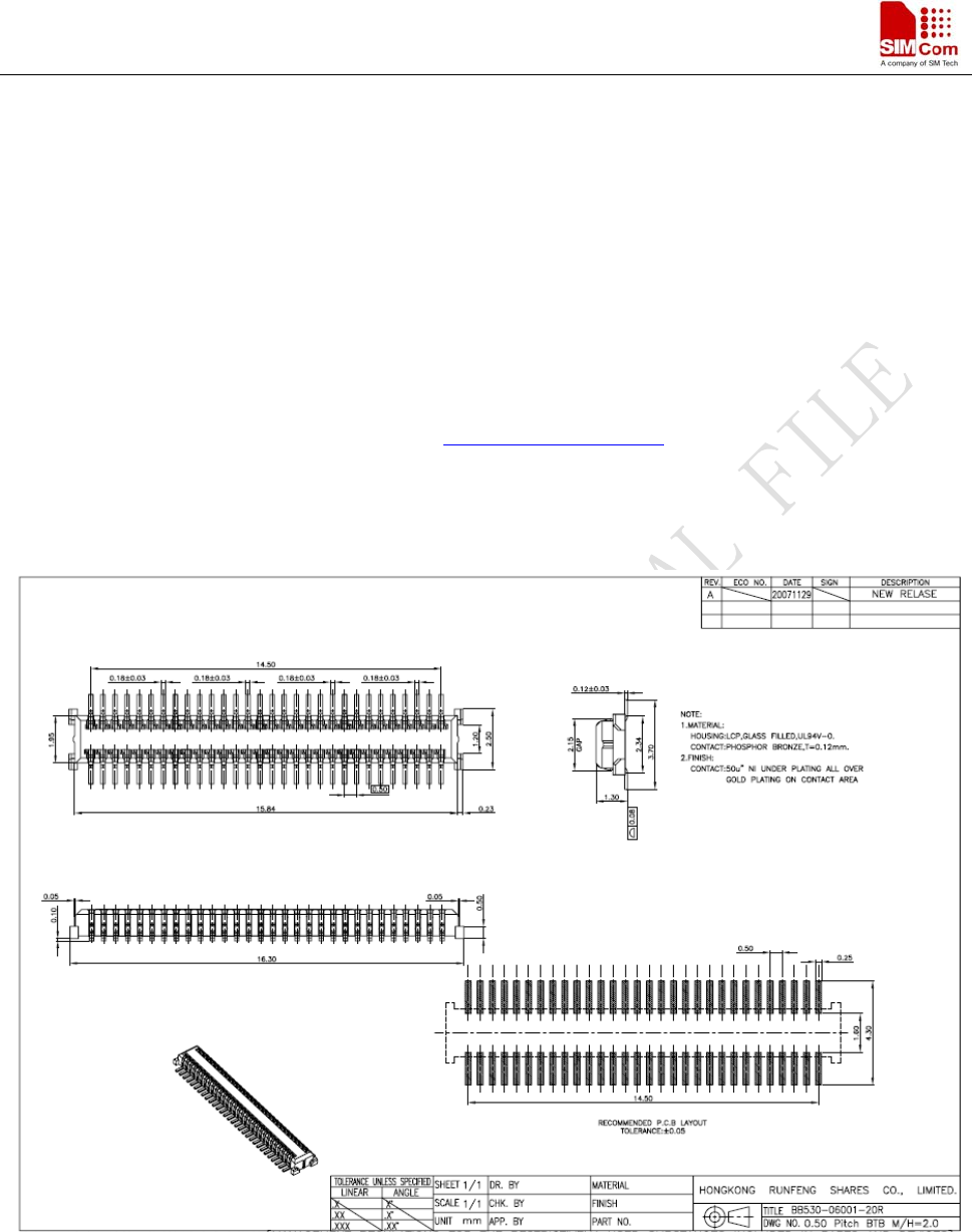
SIM900B Hardware Design
6.3 Mounting SIM900B onto the application platform
Use the connector SUNCAGEY BB530-06001-20R to fix the SIM900B onto the customer platform
6.4 Board-to-board connector
We recommend to use SUNCAGEY Company’s BB530-06001-20R as the board-to-board connector. They are
fully compatible each other. This high density SMT connector is designed for parallel PCB-to-PCB applications.
It is ideal to use in VCRs, notebook PCs, cordless telephones, mobile phones, audio/visual and other
telecommunications equipment where reduced size and weight are important. Following is parameter of
BB530-06001-20R. For more details, you can login http://www.suncagey.com for more information.
6.4.1 Mechanical dimensions of the SUNCAGEY BB530-06001-20R
Figure 36: SUNCAGEY BB530-06001-20R board-to-board connector
SIM900B_HD_V1.03 24.06.2010
57
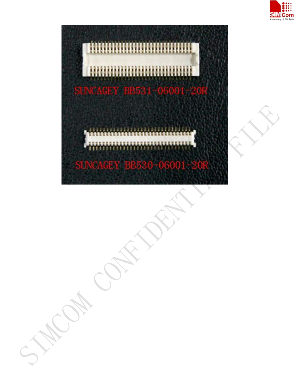
SIM900B Hardware Design
Figure 37 Board-to-board connector physical photo
SIM900B_HD_V1.03 24.06.2010
58
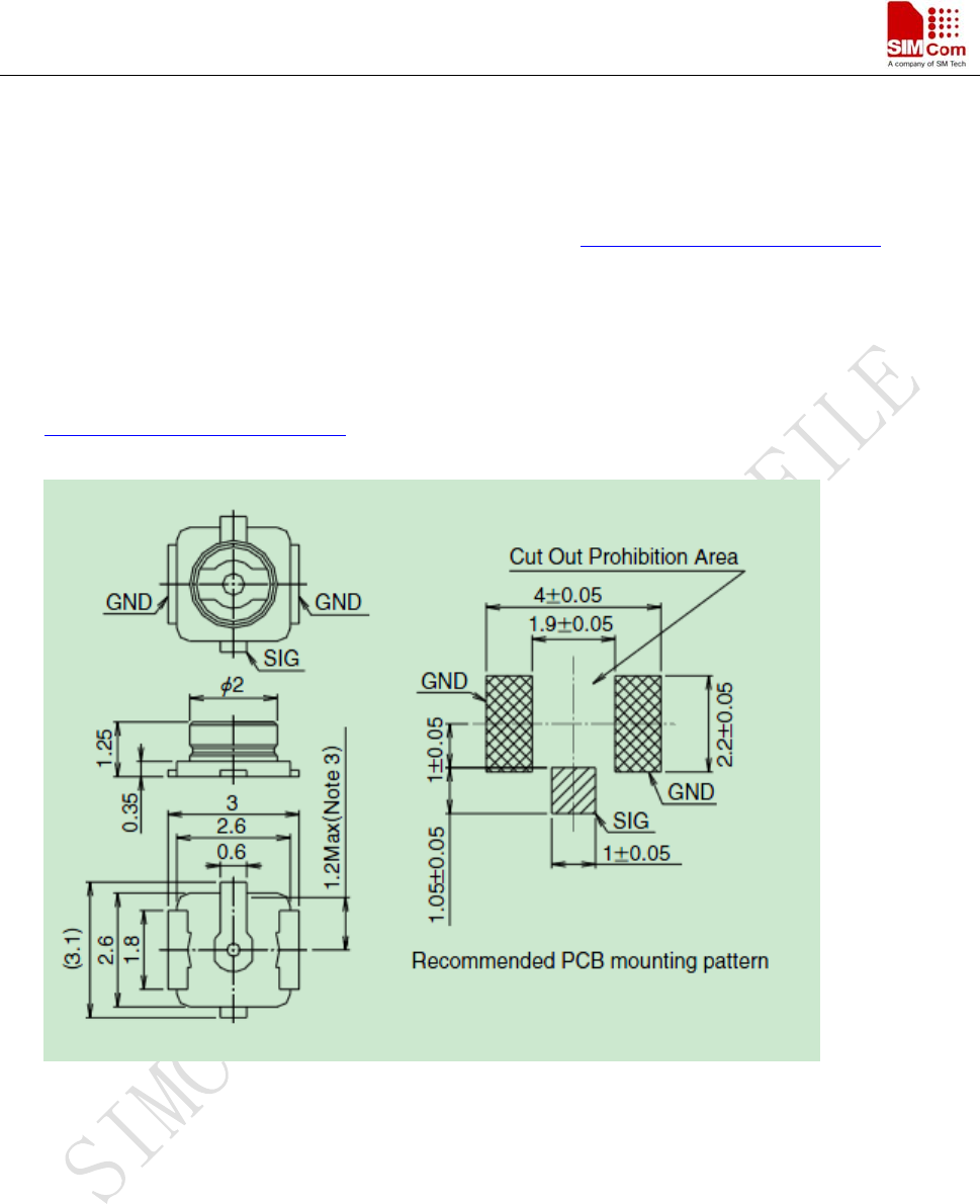
SIM900B Hardware Design
6.5 RF connector
The RF connector in module side is a ultra small surface mount coaxial connectors (Part Number: U.FL-R-SMT,
vended by HRS). It has high performance with wide frequency range, surface mountable and reflows solderable.
Following is parameter (Figure 36). Certainly the user can visit http://www.hirose-connectors.com/ for more
information.
To get good RF performance in customer’s design, we suggest the customer to use the matching RF adapter cable
which is also supplied by HRS (Part Number: U.FL-LP(V)-040), the following figure 41 is the dimensions of
U.FL series RF adapter cable. The customer can get it from the cable’s manufacturer HRS, and for details, please
visit http://www.hirose-connectors.com/.
Unit:mm
Figure 38: U.FL-R-SMT
SIM900B_HD_V1.03 24.06.2010
59
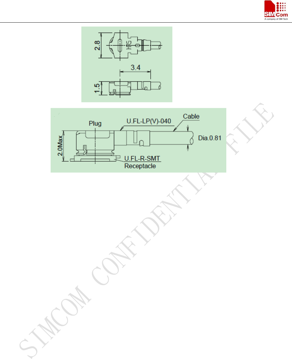
SIM900B Hardware Design
Unit:mm
Figure 39: U.FL series RF adapter cable
SIM900B_HD_V1.03 24.06.2010
60
SIM900B Hardware Design
6.6 PIN Assignment of SIM900B
Table 30: PIN assignment
PIN NO. PIN NAME I/O PIN NO. PIN NAME I/O
1 VBAT I 2 VBAT I
3 VBAT I 4 VBAT I
5 VBAT I 6 VBAT I
7 VBAT I 8 VBAT I
9 GND 10 GND
11 GND 12 GND
13 GND 14 GND
15 VRTC I/O 16 SIM_PRESENCE I
17 VDD_EXT O 18 DISP_DATA I/O
19 SIM_VDD O 20 DISP_CLK O
21 SIM_DATA I/O 22 DISP_CS O
23 SIM_CLK O 24 DISP_D/C O
25 SIM_RST O 26 DISP_RST O
27 KBC0 O 28 DCD O
29 GPIO4/KBC1 I/O 30 NETLIGHT O
31 GPIO3/KBC2 I/O 32 GPIO0 I/O
33 GPIO2/KBC3 I/O 34 PWRKEY I
35 GPIO1/KBC4 I/O 36 BUZZER O
37 KBR0 I 38 DTR I
39 GPIO9/KBR1 I/O 40 RXD I
41 GPIO8/KBR2 I/O 42 TXD O
43 GPIO7/KBR3 I/O 44 RTS I
45 GPIO6/KBR4 I/O 46 CTS O
47 DBG_RXD I 48 RI O
49 DBG_TXD O 50 AGND
51 AGND 52 ADC0 I
53 MIC1P I 54 SPK1P O
55 MIC1N I 56 SPK1N O
57 MIC2P I 58 SPK2P O
59 MIC2N I
60 SPK2N O
SIM900B_HD_V1.03 24.06.2010
61