Simcom 1009092010007 GSM/GPRS/EDGE/WCDMA module User Manual SIM5215A HD V1 02 100826
Shanghai Simcom Ltd. GSM/GPRS/EDGE/WCDMA module SIM5215A HD V1 02 100826
Simcom >
Installation instructions
Hardware Design
SIM5215A _HD_V1.02

Document Title: SIM5215A Hardware Design
Version: 1.02
Date: 2010-08-26
Status: Release
Document Control ID: SIM5215A _HD_V1.02
General Notes
SIMCOM offers this information as a service to its customers, to support application and
engineering efforts that use the products designed by SIMCOM. The information provided is
based upon requirements specifically provided to SIMCOM by the customers. SIMCOM has not
undertaken any independent search for additional relevant information, including any information
that may be in the customer’s possession. Furthermore, system validation of this product designed
by SIMCOM within a larger electronic system remains the responsibility of the customer or the
customer’s system integrator. All specifications supplied herein are subject to change.
NOTICE:
This device complies with Part 15 of the FCC Rules [and with RSS-210 of Industry Canada].
Operation is subject to the following two conditions:
(1) this device may not cause harmful interference, and
(2) this device must accept any interference received, including interference that may cause
undesired operation.
Changes or modifications made to this equipment not expressly approved by SIMCOM may void the
FCC authorization to operate this equipment.
This equipment has been tested and found to comply with the limits for a Class B digital device, pursuant
to Part 15 of the FCC Rules. These limits are designed to provide reasonable protection against
harmful interference in a residential installation. This equipment generates, uses and can radiate radio
frequency energy and, if not installed and used in accordance with the instructions, may cause harmful
interference to radio communications. However, there is no guarantee that interference will not occur in
a particular installation. If this equipment does cause harmful interference to radio or television
reception, which can be determined by turning the equipment off and on, the user is encouraged to try to
correct the interference by one or more of the following measures:
• Reorient or relocate the receiving antenna.
• Increase the separation between the equipment and receiver.
• Connect the equipment into an outlet on a circuit different from that to which the receiver is
connected.
• Consult the dealer or an experienced radio/TV technician for help.

SIM5215A _HD_V1.02 Hardware Design
SIM5215A _HD_V1.02 26.08.2010
2
This Class [B] digital apparatus complies with Canadian ICES-003.
Cet appareil numérique de la classe [*] est conforme à la norme NMB-003 du Canada.
Radiofrequency radiation exposure Information:
This equipment complies with FCC radiation exposure limits set forth for an uncontrolled environment.
This equipment should be installed and operated with minimum distance of 20 cm between the radiator
and your body.
This transmitter must not be co-located or operating in conjunction with any other antenna or transmitter.
Copyright
This document contains proprietary technical information which is the property of SIMCOM
Limited., copying of this document and giving it to others and the using or communication of the
contents thereof, are forbidden without express authority. Offenders are liable to the payment of
damages. All rights reserved in the event of grant of a patent or the registration of a utility model
or design. All specification supplied herein are subject to change without notice at any time.
Copyright © Shanghai SIMCOM Wireless Solutions Ltd. 2010
SIM5215A _HD_V1.02 Hardware Design
SIM5215A _HD_V1.02 26.08.2010
3
Version history
Data Version Description of change Author
2010-4-26 01.00 Origin
2010-07-19 01.01
Add RESET timing and module is waked up by DTR
signal description, modify the description of PCM
interface
libing
2010-08-26 01.02 Add firmware update description libing

SIM5215A _HD_V1.02 Hardware Design
SIM5215A _HD_V1.02 26.08.2010
4
Contents
Version history..............................................................................................................3
1 Introduction...............................................................................................................6
1.1 Related documents ..............................................................................................................6
1.2 Terms and abbreviations......................................................................................................7
2 Product concept.......................................................................................................10
3 Application interface...............................................................................................13
3.1 SIM5215A pin description ................................................................................................14
3.2 Operating modes ...............................................................................................................17
3.3 Power supply.....................................................................................................................18
3.3.1 Power supply pins on the board-to-board connector ....................................................................... 19
3.3.2 Minimizing power losses ................................................................................................................ 20
3.3.3 Monitoring power supply ................................................................................................................20
3.4 Power up and power down scenarios ................................................................................20
3.4.1 Turn on SIM5215A ......................................................................................................................... 20
3.4.2 Turn off SIM5215A.........................................................................................................................21
3.5 Power saving.....................................................................................................................22
3.5.1 Minimum functionality mode.......................................................................................................... 22
3.5.2 Flight mode .....................................................................................................................................23
3.5.3 Sleep Mode ..................................................................................................................................... 23
3.5.4 Wake up SIM5215A from Sleep Mode ........................................................................................... 24
3.6 RTC backup.......................................................................................................................24
3.7 Serial interface ..................................................................................................................26
3.8 Audio interfaces ................................................................................................................29
3.8.1 Speaker interface configuration....................................................................................................... 30
3.8.2 Microphone interfaces configuration .............................................................................................. 31
3.8.3 Earphone interface configuration .................................................................................................... 32
3.8.4 Referenced electronic characteristic................................................................................................ 32
3.8.5 Programming characteristic............................................................................................................. 33
3.9 USIM card interface..........................................................................................................36
3.9.1 USIM card application ....................................................................................................................36
3.9.2 Design considerations for USIM card holder .................................................................................. 37
3.10 I2C interface....................................................................................................................38
3.11 USB interface ..................................................................................................................39
3.12 Module Reset ..................................................................................................................40
3.13 General purpose input & output (GPIO) .........................................................................40
3.14 ADC interface .................................................................................................................42
3.15 LDO power output ..........................................................................................................43
3.16 Camera module interface ................................................................................................43
3.17 MMC/SD card interface..................................................................................................46
3.18 PCM Interface .................................................................................................................48

SIM5215A _HD_V1.02 Hardware Design
SIM5215A _HD_V1.02 26.08.2010
5
3.18.1 Auxiliary PCM (128 kHz PCM clock) .......................................................................................... 50
3.18.2 Primary PCM (2048 kHz PCM clock) .......................................................................................... 51
3.18.3 Transmitting PCM data by USB.................................................................................................... 53
3.19 Firmware update .............................................................................................................53
3.19.1 SD Card update ............................................................................................................................. 53
3.19.2 USB interface update. ...................................................................................................................54
4 Antenna interface....................................................................................................57
4.1 Antenna installation...........................................................................................................57
4.1.1 Antenna connector...........................................................................................................................57
4.2 Module RF output power ..................................................................................................59
4.3 Module RF receiver sensitivity .........................................................................................59
4.4 Module operating frequencies...........................................................................................59
5 Electrical, reliability and radio characteristics....................................................60
5.1 Absolute maximum ratings ...............................................................................................60
5.2 Operating temperatures .....................................................................................................60
5.3 Power supply ratings.........................................................................................................60
5.4 Current consumption.........................................................................................................61
5.5 Electro-Static discharge.....................................................................................................63
6 Mechanics ................................................................................................................65
6.1 Mechanical dimensions of SIM5215A..............................................................................65
6.2 Mounting SIM5215A onto the application platform.........................................................65
6.3 Board-to-board connector .................................................................................................67
6.4 RF connector and adapter cable ........................................................................................68
6.5 View of the SIM5215A .....................................................................................................70
6.6 PIN assignment of board-to-board connector of SIM5215A ............................................70

SIM5215A _HD_V1.02 Hardware Design
SIM5215A _HD_V1.02 26.08.2010
6
1 Introduction
This document describes the hardware interface of the SIMCOM SIM5215A module that connects
to the specific application and the air interface. As SIM5215A can be integrated with a wide
range of applications, all functional components of SIM5215A are described in great detail.
This document can help you quickly understand SIM5215A interface specifications, electrical and
mechanical details. With the help of this document and other SIM5215A application notes, user
guide, you can use SIM5215A module to design and set-up mobile applications quickly.
1.1 Related documents
Table 1: Related documents
SN Document name Remark
[1] SIMCOM_SIM5215_A
TC_EN_V1.03
SIMCOM_SIM5215_ATC_EN_V1.03
[2] ITU-T Draft new
recommendationV.25ter
:
Serial asynchronous automatic dialing and control
[3] GSM 07.07: Digital cellular telecommunications (Phase 2+); AT command
set for GSM Mobile Equipment (ME)
[4] GSM 07.10: Support GSM 07.10 multiplexing protocol
[5] GSM 07.05: Digital cellular telecommunications (Phase 2+); Use of Data
Terminal Equipment – Data Circuit terminating Equipment
(DTE – DCE) interface for Short Message Service (SMS) and
Cell Broadcast Service (CBS)
[6] GSM 11.14: Digital cellular telecommunications system (Phase 2+);
Specification of the SIM Application Toolkit for the Subscriber
Identity Module – Mobile Equipment (SIM – ME) interface
[7] GSM 11.11: Digital cellular telecommunications system (Phase 2+);
Specification of the Subscriber Identity Module – Mobile
Equipment (SIM – ME) interface
[8] GSM 03.38: Digital cellular telecommunications system (Phase 2+);
Alphabets and language-specific information
[9] GSM 11.10 Digital cellular telecommunications system (Phase 2); Mobile
Station (MS) conformance specification; Part 1: Conformance
specification
[10] 3GPP TS 51.010-1
Digital cellular telecommunications system (Release 5); Mobile
Station(MS) conformance specification
[11] 3GPP TS 34.124
Electromagnetic Compatibility (EMC) for mobile terminals and
ancillary equipment.
[12] 3GPP TS 34.121
Electromagnetic Compatibility (EMC) for mobile terminals and
ancillary equipment.
[13] 3GPP TS 34.123-1
Technical Specification Group Radio Access Network; Terminal
conformance specification; Radio transmission and reception
(FDD)
[14] 3GPP TS 34.123-3
User Equipment (UE) conformance specification; Part 3:
Abstract Test Suites.

SIM5215A _HD_V1.02 Hardware Design
SIM5215A _HD_V1.02 26.08.2010
7
[15] EN 301 908-02 V3.2.1
Electromagnetic compatibility and Radio spectrum Matters (ER
M
Stations (BS) and User Equipment (UE) for IMT-2000 Third Gen
e
cellular networks; Part 2: Harmonized EN for IMT-2000, CDMA
D
Spread (UTRA FDD) (UE) covering essential requirements of art
i
of the R&TTE Directive
[16] EN 301 489-24 V1.4.1
Electromagnetic compatibility and Radio Spectrum Matters
(ERM); Electromagnetic Compatibility (EMC) standard for
radio equipment and services; Part 24: Specific conditions for
IMT-2000 CDMA Direct Spread (UTRA) for Mobile and
portable (UE) radio and ancillary equipment
[17] IEC/EN60950-1(2006)
Safety of information technology equipment (2000)
[18] 3GPP TS 51.010-1
Digital cellular telecommunications system (Release 5); Mobile
Station (MS) conformance specification
[19] GCF-CC V3.23.1
Global Certification Forum - Certification Criteria
[20] 2002/95/EC Directive of the European Parliament and of the Council of 27
January 2003 on the restriction of the use of certain hazardous
substances in electrical and electronic equipment(RoHS)
[21] SIM52xx_Audio_Appli
cation_Note_V1.01
SIM52xx_Audio_Application_Note_V1.01
[22] SIM52xx_PCM_Applic
ation_Note_V1.02
SIM52xx_PCM_Application_Note_V1.02
[23] SIM52xx_Waking_up_
Application_Note_V1.0
3
SIM52xx_Waking_up_Application_Note_V1.03
1.2 Terms and abbreviations
Table 2: Terms and abbreviations
Abbreviation Description
ADC Analog-to-Digital Converter
ARP Antenna Reference Point
BER Bit Error Rate
BTS Base Transceiver Station
CS Coding Scheme
CSD Circuit Switched Data
CTS Clear to Send
DAC Digital-to-Analog Converter
DRX Discontinuous Reception
DSP Digital Signal Processor
DTE Data Terminal Equipment (typically computer, terminal, printer)
DTR Data Terminal Ready
DTX Discontinuous Transmission
EFR Enhanced Full Rate
EGSM Enhanced GSM
EMC Electromagnetic Compatibility
ESD Electrostatic Discharge
ETS European Telecommunication Standard

SIM5215A _HD_V1.02 Hardware Design
SIM5215A _HD_V1.02 26.08.2010
8
FCC Federal Communications Commission (U.S.)
FDMA Frequency Division Multiple Access
FR Full Rate
GMSK Gaussian Minimum Shift Keying
GPRS General Packet Radio Service
GSM Global Standard for Mobile Communications
HR Half Rate
I2C Inter-Integrated Circuit
IMEI International Mobile Equipment Identity
Inorm Normal Current
Imax Maximum Load Current
kbps Kilo bits per second
Li-Ion Lithium-Ion
MO Mobile Originated
MS Mobile Station (GSM engine), also referred to as TE
MT Mobile Terminated
PAP Password Authentication Protocol
PBCCH Packet Switched Broadcast Control Channel
PCB Printed Circuit Board
PCS Personal Communication System, also referred to as GSM 1900
RF Radio Frequency
RMS Root Mean Square (value)
RTC Real Time Clock
Rx Receive Direction
SIM Subscriber Identification Module
SMS Short Message Service
SPI serial peripheral interface
TDMA Time Division Multiple Access
TE Terminal Equipment, also referred to as DTE
TX Transmit Direction
UART Universal Asynchronous Receiver & Transmitter
VSWR Voltage Standing Wave Ratio
Vmax Maximum Voltage Value
Vnorm Normal Voltage Value
Vmin Minimum Voltage Value
VIHmax Maximum Input High Level Voltage Value
VIHmin Minimum Input High Level Voltage Value
VILmax Maximum Input Low Level Voltage Value
VILmin Minimum Input Low Level Voltage Value
VImax Absolute Maximum Input Voltage Value
VImin Absolute Minimum Input Voltage Value

SIM5215A _HD_V1.02 Hardware Design
SIM5215A _HD_V1.02 26.08.2010
9
VOHmax Maximum Output High Level Voltage Value
VOHmin Minimum Output High Level Voltage Value
VOLmax Maximum Output Low Level Voltage Value
VOLmin Minimum Output Low Level Voltage Value
FD SIM fix dialing phonebook
SM SIM phonebook
NC Not connect
EDGE Enhanced data rates for GSM evolution
HSDPA High Speed Downlink Packet Access
HSUPA High Speed Uplink Packet Access
ZIF Zero intermediate frequency
WCDMA Wideband Code Division Multiple Access
VCTCXO Voltage control temperature-compensated crystal oscillator
USIM Universal subscriber identity module
UMTS Universal mobile telecommunications system
UART Universal asynchronous receiver transmitter
A-GPS Assisted Global positioning system
GPS Global positioning system
S-GPS Simultaneous Global positioning system

SIM5215A _HD_V1.02 Hardware Design
SIM5215A _HD_V1.02 26.08.2010
10
2 Product concept
Designed for global market, SIM5215A is a quad-band GSM/GPRS/EDGE and dual-band UMTS
engine that works on frequencies of GSM 850MHz, EGSM 900 MHz, DCS 1800 MHz, PCS
1900MHz, and WCDMA 1900M/850M. SIM5215A provides GPRS multi-slot class
12/class10/class 8 (optional) capability and EDGE, supports the GPRS coding schemes CS-1,
CS-2, CS-3 and CS-4. EDGE: 8 PSK, DTM (class A) multi-slot class 12, DL coding schemes:
MCS1-9, UL coding schemes: MCS1-9.
With a tiny configuration of 36mm × 26mm × 4.5 mm, SIM5215A can fit almost all the
space requirements in your applications, such as AMR, POS, Security & Surveillance and other
mobile devices.
The physical interface to the mobile application is made through a 70 pins board-to-board
connector, which provides all hardware interfaces between the module and customers’ boards
except the RF antenna interface.
z Serial port and USB 2.0 port can be alternatively used as data port.
z USIM interface: support SIM cards: 3V & 1.8V
z Power on/off and reset signal
z Backup RTC interface.
z Six GPIOs: 1 for interrupt, 1 for flight mode, 1 for status LED, 2 for output control, 1
for input, also can be multiplex as a PCM interface.
z Three audio channels include two microphones inputs and three audio outputs. This can
be easily configured by AT command.
z A camera interface is provided,(if above pins are not used as camera interface ,it could
be configured as GPIOs..
z An I2C interface is provided.
z An ADC interface
z A LDO power output
z A 4 bit SD card interface
z A PCM interface, all pins of PCM interface can be configured as GPIOs(default are
GPIOs).
The SIM5215A provides RF antenna interface with two alternatives: antenna connector and
antenna pad. The antenna connector is MURATA MM9329-2700. And customer’s antenna can be
soldered to the antenna pad.
The SIM5215A is integrated with the TCP/IP protocol,Extended TCP/IP AT commands are
developed for customers to use the TCP/IP protocol easily, which is very useful for those data
transfer applications. FTP/HTTP/ SMTP/POP3/ MMS/ LUA Script is integrated in SIM5215A
too.
Note: The SIM5215A has two kinds of interface (UART and USB) to connect to host CPU.

SIM5215A _HD_V1.02 Hardware Design
SIM5215A _HD_V1.02 26.08.2010
11
USB interface is mapped to five virtual ports: “SIMTECH USB Modem”, “SIMTECH NMEA
Device”, “SIMTECH ATCOM Device”, “SIMTECH Diagnostics interface” and “SIMTECH
Wireless Ethernet Adapter”. UART, “SIMTECH USB Modem” and “SIMTECH ATCOM
Device” could respond to AT command, and URC report to these three ports at the same time,
but user could set dedicated port to receive URC (Unsolicited Result Code).
SIM5215A key features at a glance:
Table 3: SIM5215A key features
Feature Implementation
Power supply Single supply voltage 3.4V – 4.2V
Power saving Please refer to Table 39
Frequency bands
z GSM: 850M/ 900M/ DCS 1800M /PCS 1900M
z WCDMA: 1900M/850M
z The SIM5215A can worked in GSM and WCDMA mode
z The frequency bands also can be set by AT + CNMP.
Transmit power ●Class 4 (+33dBm ±2dB) for GSM850
●Class 4 (+33dBm ±2dB) for EGSM900
●Class 1 (+30dBm ±2dB) for GSM1800
●Class 1 (+30dBm ±2dB) for GSM1900
●Class E2 (+27dBm ± 3dB) for GSM 850 8-PSK
●Class E2 (+27dBm ± 3dB) for GSM 900 8-PSK
●Class E2 (+26dBm +3 /-4dB) for GSM 1800 8-PSK
●Class E2 (+26dBm +3 /-4dB) for GSM 1900 8-PSK
●Class 3 (+24dBm +1.7/-3.7dB) for WCDMA 1900, WCDMA FDD
BDII
●Class 3 (+24dBm +1.7/-3.7dB) for WCDMA 850, WCDMA FDD
BDV
GPRS/EDGE
connectivity
z GPRS/EDGE multi-slot is up to class 12
z GPRS mobile station class B
Temperature range
z Operating Temperature: -30°C to +80°C
z Storage temperature -40°C to +85°C
DATA GPRS:
z GPRS data downlink transfer: max. 85.6 kbps
z GPRS data uplink transfer: max. 42.8 kbps
z Coding scheme: CS-1, CS-2, CS-3 and CS-4
z SIM5215A supports the protocols PAP (Password Authentication
Protocol) usually used for PPP connections.
z The SIM5215A integrates the TCP/IP protocol.
z Support Packet Switched Broadcast Control Channel (PBCCH)
z CSD transmission rates: 2.4, 4.8, 9.6, 14.4 kbps, non-transparent
z Unstructured Supplementary Services Data (USSD) support
DATA EDGE z EDGE E2 power class for 8 PSK
z DTM (simple class A), multi-slot class 12
z Downlink coding schemes – MCS 1-9
z Uplink coding schemes – MCS 1-9

SIM5215A _HD_V1.02 Hardware Design
SIM5215A _HD_V1.02 26.08.2010
12
z BEP reporting and test mode B
z 8-bit, 11-bit RACH
z PBCCH support
z phase/2 phase access procedures
DATA UMTS z R99
z
SMS z MT, MO, CB, Text and PDU mode
z SMS storage: SIM card
z Support transmission of SMS alternatively over CSD or GPRS.
User can choose preferred mode.
SIM interface Support SIM card: 1.8V ,3V
External antenna Connected via 50 Ohm antenna connector or antenna pad
Audio features Speech codec modes:
z Half Rate (ETS 06.20)
z Full Rate (ETS 06.10)
z Enhanced Full Rate (ETS 06.50 / 06.60 / 06.80)
z AMR(WCDMA)
z AMR+QCP(GSM)
z A5/1, A5/2, and A5/3 ciphering
Serial interface z Serial Port standard or null modem mode on Serial Port Interface
z Serial Port can be used to control module by sending AT
command.
Phonebook
management
Support phonebook types: SM, FD, LD, RC, ON, MC.
SIM Application
Toolkit
Support SAT class 3, GSM 11.14 Release 98
Support USAT
Real time clock Implemented
Timer function Programmable via at command
Physical characteristics Size: 36 mm ×26mm ×4.5 mm
Weight: 7g
Firmware upgrade Firmware upgrade over USB interface
PCM Multiplex on GPIOs. 3 formats: 8 bit (υ-law or A-law) and 16 bit
(linear).
Table 4:Coding schemes and maximum net data rates over air interface
Coding scheme 1 Timeslot 2 Timeslot 4 Timeslot
CS-1: 9.05kbps 18.1kbps 36.2kbps
CS-2: 13.4kbps 26.8kbps 53.6kbps
CS-3: 15.6kbps 31.2kbps 62.4kbps
CS-4: 21.4kbps 42.8kbps 85.6kbps
MCS-1 8.80kbps 17.60kbps 35.20kbps
MCS-2 11.2kbps 22.4kbps 44.8kbps
MCS-3- 14.8kbps 29.6kbps 59.2kbps
MCS-4 17.6kbps 35.2kbps 70.4kbps
MCS-5 22.4kbps 44.8kbps 89.6kbps
SIM5215A _HD_V1.02 Hardware Design
SIM5215A _HD_V1.02 26.08.2010
13
MCS-6 29.6kbps 59.2kbps 118.4kbps
MCS-7 44.8kbps 89.6kbps 179.2kbps
MCS-8 54.4kbps 108.8kbps 217.6kbps
MCS-9 59.2kbps 118.4kbps 236.8kbps
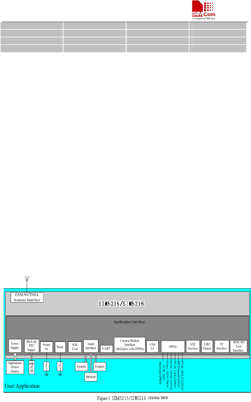
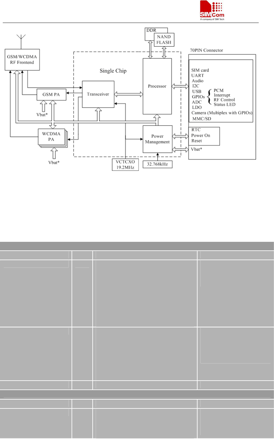
3 Application interface
All hardware interfaces except RF interface that connects SIM5215A to the customers’ cellular
application platform is through a 70-pin 0.4mm pitch board-to-board connector. Figure 1 is
SIM5215A system overview. Figure 2 is SIM5215A block diagram. Sub-interfaces included in
this board-to-board connector are described in detail in following chapters:
z Power supply
z USB interface
z Serial interface
z Analog audio interfaces
z SIM interface
z GPIO
z ADC
z LDO Power output
z PCM interface
z MMC/SD interface
z Camera interface
z RTC
z I2C interface
Electrical and mechanical characteristics of the board-to-board connector are specified in
Chapter 6. There we also order information for mating connectors.
SIM5215A _HD_V1.02 Hardware Design
SIM5215A _HD_V1.02 26.08.2010
14
Figure 2:SIM5215A block diagram
3.1 SIM5215A pin description
Table 5:Board-to-Board Connector pin description
Power Supply
PIN NAME I/O DESCRIPTION DC CHARACTERISTICS
VBAT Six BAT pins of the board-to-board
connector are dedicated to connect
the supply voltage. The power supply
of SIM5215A has to be a single
voltage source of VBAT= 3.3V...4.2V.
It must be able to provide sufficient
current in a transmit burst which
typically rises to 2A. Mostly, these
six pins are voltage input
Vmax= 4.2V
Vmin=3.4V
Vnorm=3.8V
VRTC Current input for RTC when the
battery is not supplied for the system.
Current output for backup battery
when the main battery is present and
the backup battery is in low voltage
state. If not in use, left it open.
Vmax=3.2V
Vnorm=3.0V
Vmin=1.5V
Inorm= 1.1uA
GND Digital ground
Power on or power off
PIN NAME I/O DESCRIPTION DC CHARACTERISTICS
POWER_ON I Voltage input for power on key.
POWER_ON get a low level voltage
for user to power on or power off the
system. It has been pulled up to
VILmax=0.2*VBAT
VIHmin=0.6*VBAT
VImax=VBAT

SIM5215A _HD_V1.02 Hardware Design
SIM5215A _HD_V1.02 26.08.2010
15
VBAT in module. The user should
keep it to low level for at least 64mS
when power on or power off the
system because the system needs
margin time to assert the software.
Audio interfaces
PIN NAME I/O DESCRIPTION DC CHARACTERISTICS
MIC_P
MIC_N
I Positive and negative voice-band
input If not in use, connect to ground
through a 100N capacitor.
Audio DC Characteristics
refer to chapter 3.8.4
HP_MICP I Auxiliary positive voice-band input,
if not in use, connect to ground
through a 100N capacitor.
EAR_P
EAR_N
O Positive and negative voice-band
output, if not in use ,left open
HPR
HPL
O Auxiliary right channel and left
channel voice-band output, if not in
use, left open.
SPK_P
SPK_N
O Loud Speaker Output, if not in
use ,left open
HKADC I Analog Digital Converter Input
VREG_AUX O LDO power output This LDO default output
voltage is 2.85V, and
driver current is rated for
250mA.
USB
PIN NAME I/O DESCRIPTION DC CHARACTERISTICS
USB_VBUS I USB power supply input, if not in
use, left open.
Vmax =5.25 V
Vmin =4.4 V
Vnor
m
= 5.0 V
USB_DP I/O Plus (+) line of the differential,
bi-directional USB signal to/from the
peripheral device. If not in use, left
open.
USB_DM I/O Minus (-) line of the differential,
bi-directional USB signal to/from the
peripheral device. If not in use, left
open.
They are compliant with
the USB 2.0 specification.
Serial interface
PIN NAME I/O DESCRIPTION DC CHARACTERISTICS
UART_DTR I Data Terminal Ready, if not in use,
left open.
UART_RXD I Receive Data, which has been pulled
down with a 15kR resistor to ground
in module, if not in use, left open. So
please don’t pull up or pull down in
y
our a
pp
lication circuit.
VILmin=0V
VILmax=0.3*VDD_EXT*
VIHmin=0.7*VDD_EXT
VIHmax=VDD_EXT+0.3
VOLmin=GND
VOLmax=0.2V

SIM5215A _HD_V1.02 Hardware Design
SIM5215A _HD_V1.02 26.08.2010
16
UART_TXD O Transmit Data, if not in use, left open.
UART_RTS O Request to Send, if not in use, left
open.
UART_CTS I Clear to Send, if not in use, left open.
UART_RI O Ring Indicator, if not in use, left
open.
UART_DCD O Data Carrier detection, if not in use,
left open.
Camera interface
PIN NAME I/O DESCRIPTION DC CHARACTERISTICS
CAM_D2 I Bit 2 of RGB or YUV D0 video
component input
CAM_D3 I Bit 3 of RGB or YUV D1 video
component input
CAM_D4 I Bit 4 of RGB or YUV D2 video
component input
CAM_D5 I Bit 5 of RGB or YUV D3 video
component input
CAM_D6 I Bit 6 of RGB or YUV D4 video
component input
CAM_D7 I Bit 7 of RGB or YUV D5 video
component input
CAM_D8 I Bit 8 of RGB or YUV D6 video
component input
CAM_D9 I Bit 9 of RGB or YUV D7 video
component input
CAM_HSYNC I Video horizontal line synchronization
signal input
CAM_VSYNC I Vertical sync input
CAM_CLK O master clock output
CAM_PCLK I Pixel clock input
CAM_RESET O Master reset out, active low
CAM_STANDBY O Power-down mode selection
“0”=Normal mode, “1”=Power-down
mode
VILmin=0V
VILmax=0.3*VDD_EXT*
VIHmin=0.7*VDD_EXT
VIHmax=VDD_EXT+0.3
VOLmin=GND
VOLmax=0.2V
VOHmin=VDD_EXT-0.2
VOHmax=VDD_EXT
All camera pins can be
configured as GPIOs.
Detail description refer to
chapter 3.16.
USIM interface
PIN NAME I/O DESCRIPTION DC CHARACTERISTICS
V_USIM O Voltage Supply for SIM card The voltage can be
selected by software to be
either 1.8V or 3V
USIM_DATA I/O SIM Data Output/Input, which has
been pulled up with a 22kR resistor to
V_USIM in module. So please do not
pull up or pull down in your
application circuit.
USIM_CLK O SIM Clock
VILmin=0V
VILmax=0.3*V_USIM
VIHmin=0.7* V_USIM
VIHmax=V_USIM +0.3
VOLmin=GND
VOLmax=0.2V

SIM5215A _HD_V1.02 Hardware Design
SIM5215A _HD_V1.02 26.08.2010
17
USIM_RESET O SIM Reset
IIC interface
PIN NAME I/O DESCRIPTION DC CHARACTERISTICS
IIC_SDA I/O I2C data, if not in use, left open. It
has been pulled up with a 2.2kR
resistor to 2.6V in module. So there is
no need to pull up it in your
application circuit.
IIC_SCL O I2C clock output, if not in use, left
open. It has been pulled up with a
2.2kR resistor to 2.6V in module. So
there is no need to pull up it in your
application circuit.
Other interface
PIN NAME I/O DESCRIPTION DC CHARACTERISTICS
Reset I System reset in, active low. Reset pin has been pulled
up in SIM5215A. Detail
description refer to chapter
3.12.
GPIO0/PCM_DIN I General Input PIN with interrupt. If
not in use, left open. It also can be
multiplexed as the PCM_DIN pin.
GPIO1 O Status Indicating LED Control.
GPIO2/PCM_SYNC I General Input PIN. If not in use, left
open. It also can be multiplexed as
the PCM_SYNC pin.
GPIO3/PCM_CLK O General Output PIN. If not in use, left
open. It also can be multiplexed as
the PCM_CLK pin.
GPIO4 I RF Control: Flight Modem switch
GPIO5/PCM_DOUT O General Output PIN. If not in use, left
open. It also can be multiplexed as
the PCM
_
DOUT
p
in.
VIHmin=0.7*VDD_EXT*
VIHmax= VDD_EXT+0.3
VOLmin=GND
VOLmax=0.2V
VOHmin= VDD_EXT-0.2
VOHmax= VDD_EXT
*Note: module internal reference supply power: VDD_Ext=2.6V
3.2 Operating modes
The following table summarizes the various operating modes, each operating modes will be
referred to in the following chapters.
Table 6:Overview of operating modes
Mode Function
Normal operation
Module Power
Off mode
Module will go to Power off mode when the Power on pin has
been pushed low for 2 Seconds.

SIM5215A _HD_V1.02 Hardware Design
SIM5215A _HD_V1.02 26.08.2010
18
Module sleep Module will automatically go into sleep mode when there is
no interrupt input or other operation.
In this case, the current consumption of module will be
reduced to the minimal level.
GSM IDLE Software is active. Module has registered to the GSM network,
and the module is ready to send and receive.
GSM mode
GSM TALK
CSD connection is going on between two subscribers. In this
case, the power consumption depends on network settings
such as DTX off/on, FR/EFR/HR, hopping sequences,
antenna.
GPRS IDLE Module is ready for GPRS data transfer, but no data is
currently sent or received. In this case, power consumption
depends on network settings and GPRS configuration (e.g.
multi-slot settings).
GPRS mode
GPRS DATA There is GPRS data in transfer (PPP or TCP or UDP). In this
case, power consumption is related with network settings (e.g.
power control level), uplink/downlink data rates and GPRS
configuration (e.g. used multi-slot settings).
EDGE mode EDGE IDLE Module is ready for data transfer in EDGE mode, but no data
is currently sent or received. In this case, power consumption
depends on network settings and EDGE configuration
EDGE mode EDGE DATA There is data in transfer (PPP or TCP or UDP) in EDGE mode.
In this case, power consumption is related with network
settings (e.g. power control level), uplink/downlink data rates
and EDGE configuration.
WCDMA
IDLE
Module has registered to the WCDMA network, and the
module is ready to send and receive.
WCDMA mode
WCDMA talk Module is active in WCDMA mode. The power consumption
depends on network settings.
POWER DOWN Normal shutdown is by sending the “AT+CPOF” command or using the
POWER_ON pin. The power management ASIC disconnects the power supply
from the base band part of the module, only the power supply for the RTC is
remained. Software is not active. The serial interfaces are not accessible.
Operating voltage (connected to VBAT) remains applied.
Minimum
functionality mode
(flight mode)
Use of the “AT+CFUN” command can set the module to a minimum
functionality mode without remove the power supply. In this case, disable phone
both transmit and receive RF circuits, that is to say ,flight mode
3.3 Power supply
The power supply of SIM5215A is from a single voltage source of VBAT= 3.3V...4.2V. In
some cases, the ripple in a transmit burst may cause voltage drops when current consumption
rise typically to peak of 2A. So the power supply must be able to provide sufficient current
up to 2A.
For the VBAT input, a local bypass capacitor is recommended. A capacitor (about 100µF, low
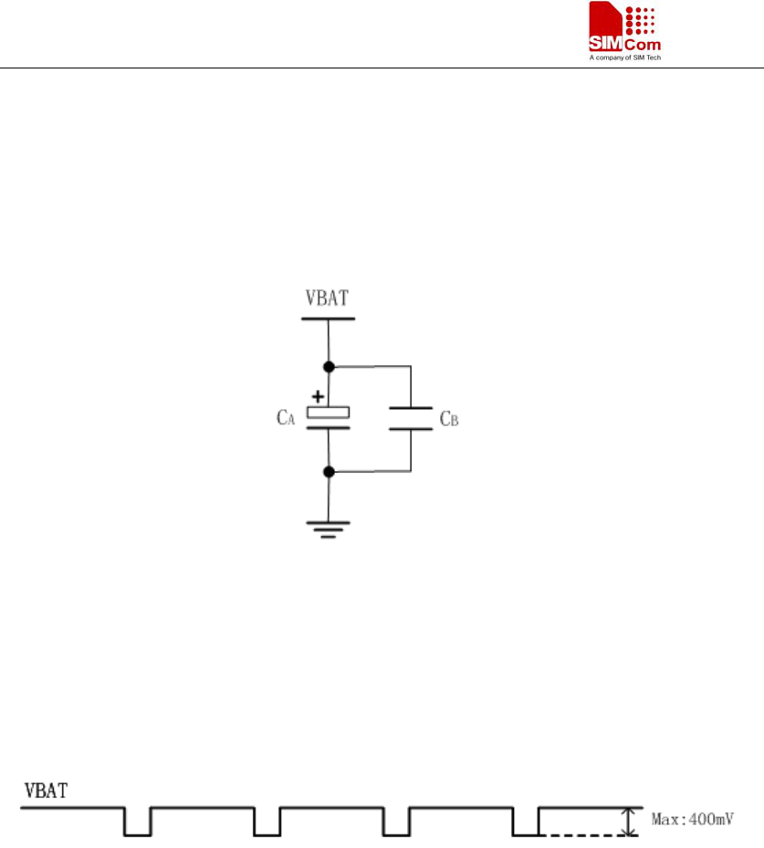
SIM5215A _HD_V1.02 Hardware Design
SIM5215A _HD_V1.02 26.08.2010
19
ESR) is recommended when one uses a Li battery. When you use a DC supply the Capacitor
must be a larger one (for example 2200u/10V), Multi-layer ceramic chip (MLCC) capacitors can
provide the best combination of low ESR and small size but may not be cost effective. A lower
cost choice may be a 100 µF tantalum capacitor (low ESR) with a small (0.1 µF to 1µF) ceramic
in parallel, which is illustrated as following figure. And the capacitors should put as closer as
possible to the SIM5215A VBAT pins. The following figure is the recommended circuit.
Figure 3:VBAT input
The following figure is the VBAT voltage ripple wave at the maximum power transmit phase,
the test condition is VBAT=4.0V, VBAT maximum output current =2A, CA=100 µF tantalum
capacitor (ESR=0.7Ω) and CB=1µF.
Figure 4:VBAT voltage drop at the maximum power transmit phase (GSM)
And make sure that the capacitor is close to VBAT pins of 70 pins connector. If a DC/DC or
LDO is used for power supply of the module, you should make sure that the peak current of power
supply can rise up to 2A (4.0V). The reference design is putting one big capacitor at the output
of the DC/DC or LDO, and another big capacitor beside the 70 pins connector.
Note: If a DC/DC or LDO is used as power supply, besides a big capacitor close to the 70-pin
connector, another big capacitor (typically a 100 µF tantalum capacitor) is suggested to be put
at the output pin of the DC/DC or LDO.
3.3.1 Power supply pins on the board-to-board connector
Six VBAT pins of the board-to-board connector are dedicated to connect the supply voltage; six
GND pins are recommended for grounding. VRTC pin can be used to back up the RTC.
SIM5215A _HD_V1.02 Hardware Design
SIM5215A _HD_V1.02 26.08.2010
20
3.3.2 Minimizing power losses
Please pay special attention to the supply power when you are designing your applications.
Please make sure that the input voltage will never drop below 3.3V even in a transmit burst
during which the current consumption may rise up to 2A. If the power voltage drops below
3.3V, the module may be switched off. Using the board-to-board connector will be the best
way to reduce the voltage drops. You should also remove the resistance from the power
supply lines on the host board or from battery pack.
3.3.3 Monitoring power supply
To monitor the supply voltage, you can use the AT command(AT+CBC) which include two
parameters: voltage supply status and voltage value (in mV). It returns the battery voltage of
1-100 percent of capacity and actual value measured at VBAT and GND.
The voltage is continuously measured at intervals depending on the operating mode. The
displayed voltage (in mV) is averaged over the last measuring period before the AT command was
executed.
3.4 Power up and power down scenarios
3.4.1 Turn on SIM5215A
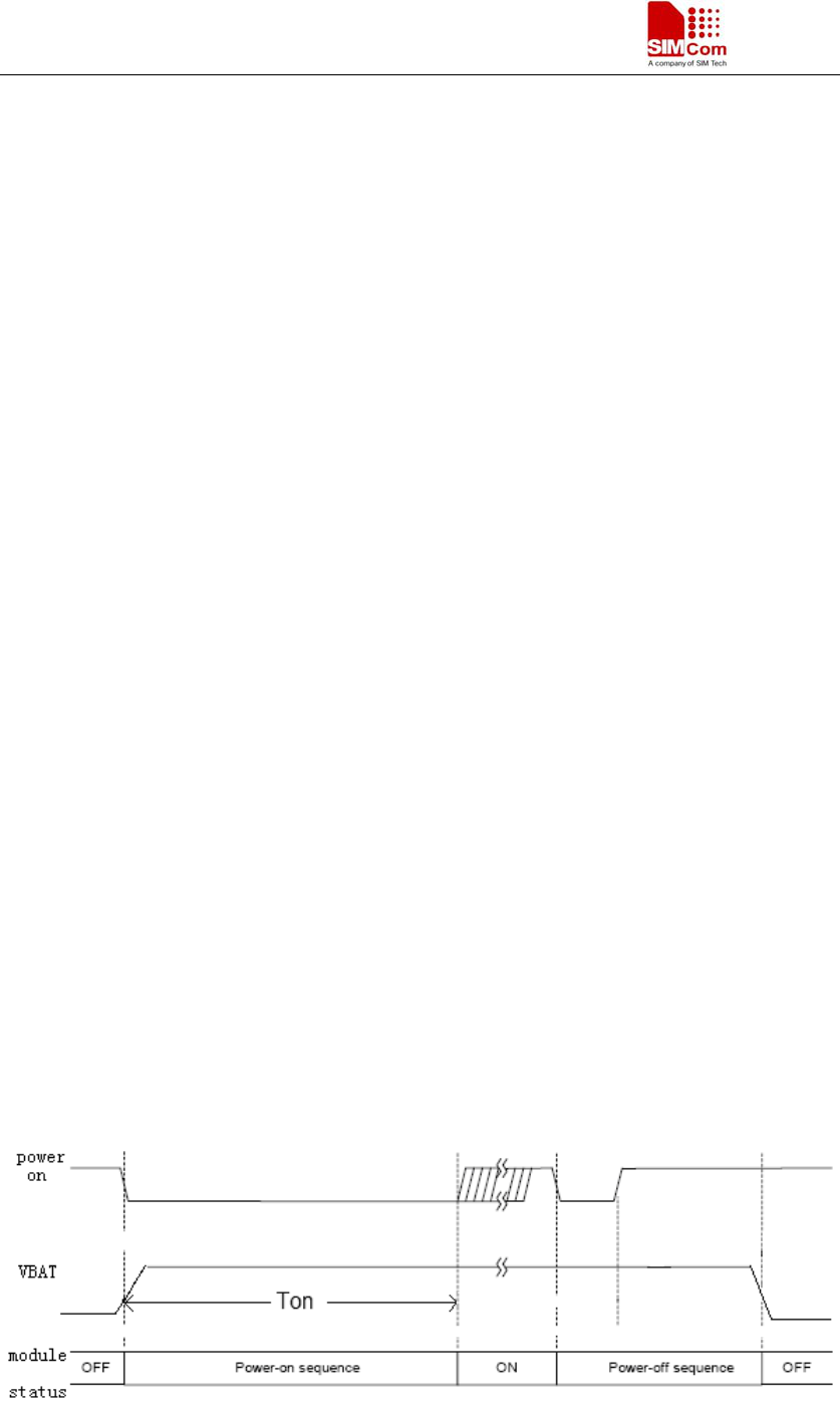
SIM5215A can be turned on by various ways, which are described in the following chapters:
z Via POWER_ON pin: starts normal operating mode;
POWER_ON has been pulled up to VBAT in module. You can turn on the SIM5215A by driving
the POWER_ON to a low level voltage for period time. The power on scenarios illustrate as
following figure.
Figure 5: Timing of turn on system
SIM5215A _HD_V1.02 Hardware Design
SIM5215A _HD_V1.02 26.08.2010
21
Note1: Ton >= 64ms.
Note2: Commonly, the AT command can be set 2-3S after the SIM5215A is powered on.
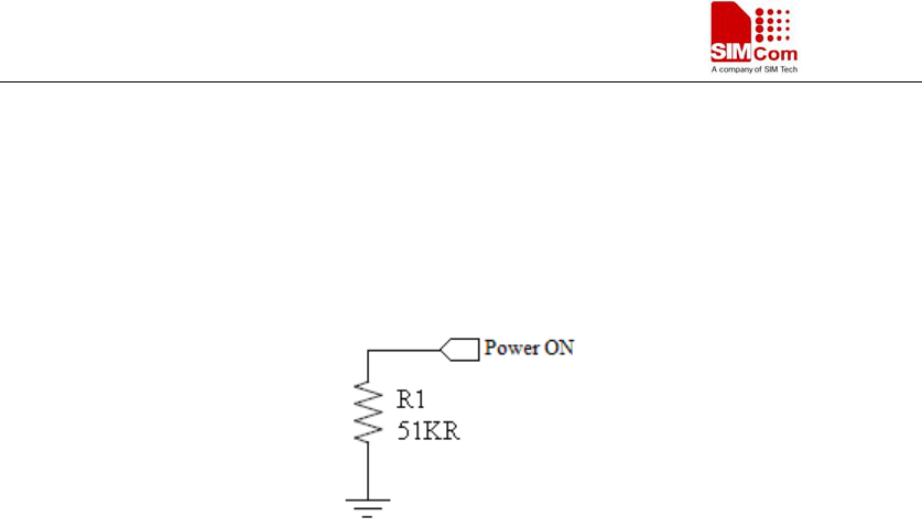
If VBAT was supplied to SIM5215A, SIM5215A could be automatically powered on by
connecting the Power ON pin to Low level directly. In automatically powering on mode, it is
suggested that the SIM5215A should reset by RESET pin after power on. Below is the reference
circuit.
Figure 6: Automatic power on
Note: The POWER_ON has been pulled up with a 250kR resistor to VBAT in module. Make
sure that VILmax=0.2*VBAT, and the value of R1 above can be changed as you want.
In automatically powering on mode, it is suggested that the SIM5215A should reset by RESET
pin after power on.
3.4.2 Turn off SIM5215A
Following procedure can be used to turn off the SIM5215A:
z Normal power down procedure: Turn off SIM5215A using the POWER_ON pin
z Normal power down procedure: Turn off SIM5215A using AT command
3.4.2.1 Turn off SIM5215A using the POWER_ON pin (Power down)
You can turn off the SIM5215A by driving the POWER_ON to a low level voltage for period
time. The low level period of the POWER_ON is about 64mS.
This procedure will let the module to be logged off from the network and allow the software to
enter into a secure state and save data before completely disconnecting the power supply.
3.4.2.2 Turn off SIM5215A using AT command
You can use AT command “AT+CPOF” to turn off the module. This command will let the
module to be logged off from the network and allow the software to enter into a secure state and
save data before completely disconnecting the power supply.
After this moment, the AT commands can not be executed. The module enters the POWER
DOWN mode, only the RTC is still active.
Please refer to AT command manual for details of the AT command “AT+ C PO F”.

SIM5215A _HD_V1.02 Hardware Design
SIM5215A _HD_V1.02 26.08.2010
22
3.4.2.3 Under-voltage automatic warning
Software will constantly monitor the voltage applied on the VBAT, if the measured battery voltage
is no more than 3.4V, the following URC will be presented:
warning! voltage is low : 3.3v
Note: Under-voltage automatic warning function default is disabled. One can enable it by
AT+CVALARM.
3.4.2.4 Under-voltage automatic shutdown
Besides the Under-voltage automatic warning, system will monitor the working voltage and power
off the module if the voltage is lower to a specified value which can be set by AT+CPMVT in
order to protect the module.
Note: this feature default is disabled, One can use AT+CPMVT to active it.
At this moment, no more AT commands can be executed. The module will be logged off from
the network and enters POWER DOWN mode, only the RTC is still active (if backup battery is
connected to VRTC pin).
3.5 Power saving
There are two methods to achieve SIM5215A module extreme low power. “AT+CFUN” is used to
set module into minimum functionality mode and GPIO4 hardware interface signal can be used to
set system to be Flight mode (Close RF).
3.5.1 Minimum functionality mode
Minimum functionality mode reduces the functionality of the module to a minimum and, thus,
minimizes the current consumption to the lowest level. This mode is set with the “AT+CFUN”
command which provides the choice of the functionality levels <fun>=0,1,4
z 0: minimum functionality, (same as CFUN=4,disable both transmit and receive RF circuits
of the phone);
z 1: full functionality (Default);
z 4: disable both transmit and receive RF circuits of the phone;
If SIM5215A has been set to minimum functionality by “AT+CFUN”, then the RF function
function will be closed, in this case, the serial port is still accessible, but all AT commands referred
to RF function or SIM card function will not be accessible.
When SIM5215A is in minimum functionality or has disabled all RF functionality by
“AT+CFUN”, it can return to full functionality by “AT+CFUN”, not need to reset module.
NOTE: In fact, Flight mode is identical with minimum functionality mode .Different titles lie
SIM5215A _HD_V1.02 Hardware Design
SIM5215A _HD_V1.02 26.08.2010
23
on different viewpoint. Flight mode is titled from visual application; however, minimum
functionality is derived from normal 3GPP at-command spec.
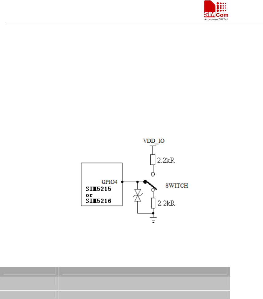
3.5.2 Flight mode
Through GPIO4 signal control SIM5215A module to enter or exit the Flight mode in customer
applications. In Flight mode, SIM5215A closes RF function. If GPIO4 is left open, SIM5215A
enters normal mode. But it is suggested that GPIO4 should not be left open. Because GPIO4 is
sensitive to ESD, so bidirectional ESD protection component is suggested to add on GPIO4.
Figure 7: Flight mode switch
Table 7:logic of flight mode switch
3.5.3 Sleep Mode
If periphery equipment stops working, and there is no on air or audio activity required and no
hardware interrupt (such as GPIO interrupt or data on serial port), SIM5215A will enter SLEEP
mode automatically. In this mode, SIM5215A can still receive paging or SMS from network. If
USB interface of SIM5215A is connecting with host CPU,and host CPU support USB suspend
mode, SIM5215A could enter sleep mode. Otherwise SIM5215A could not enter sleep mode.
GPIO4 Status Module Action
Low Level Flight Mode: RF is closed.
High Level Normal Mode: RF is working.

SIM5215A _HD_V1.02 Hardware Design
SIM5215A _HD_V1.02 26.08.2010
24
3.5.4 Wake up SIM5215A from Sleep Mode
When SIM5215A is in SLEEP mode, the following method can wake up the module.
z USB interface active
z Receive a voice or data call from network to wake up SIM5215A.
z Receive a SMS from network to wake up SIM5215A.
z Receive a interrupt signal from GPIO0
z GPIO4 state change.
z Receive AT command from UART.
z UART DTR signal changed.
Normally DTR pin will stay high but in certain condition when serial port is used in Null
Modem(3-line mode). When host wants to wake up SIM5215A, it can pull down DTR for about
12ms(since SIM5215A has a debounce time of 10ms for mistaken interrupt checking). Then DTR
will trigger an interrupt which will finally cause SIM5215A to be waken up from sleep mode.
Note: One can enable/disable such function by AT+CDTRISRS, also One can configure the
DTR’s trigger condition by AT+CDTRISRMD(only level trigger condition has debounce time).
Currently the function is enabled by default and the trigger condition is low level. Please
reference document [23] for detailed information of Waking_up_Application_Note.
WARNING!!!: when DTR has been pulled down/up long enough to trigger the interrupt one
must recover DTR to original status or the interrupt will be triggered all the time and SIM5215A
may crash.
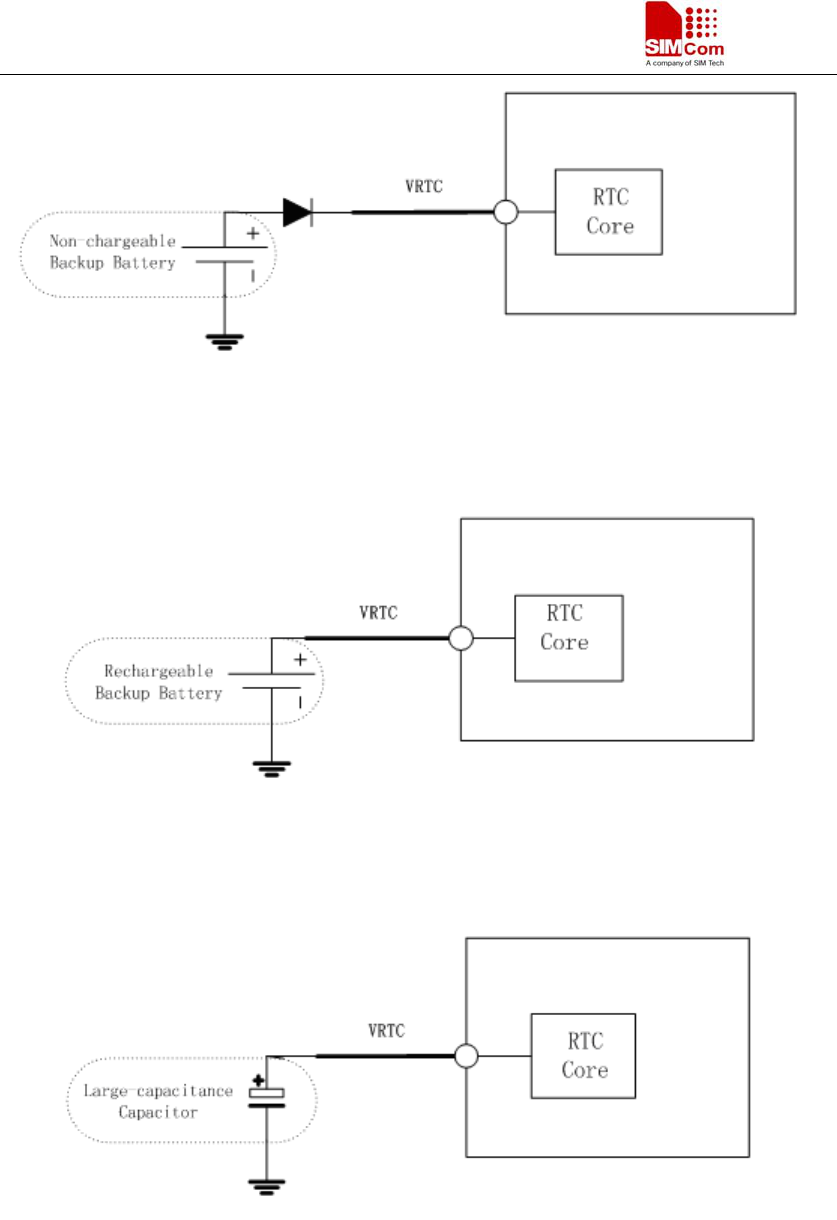
3.6 RTC backup
The RTC (Real Time Clock) power supply of module can be provided by an external battery or a
battery (rechargeable or non-chargeable) through the VRTC (PIN11) on the board-to-board
connector. You need only a coin-cell battery or a super-cap to VRTC to backup power supply for
RTC. The discharge current is smaller than 10uA. The module could update local time based
on universal time and time zone from network. (This feature must be supported by the network).
If this feature is used, please refer to AT command AT+CTZU and AT +CTZR.
Note: The VRTC default state can be designed to a NC pin in your circuit. If you need to use
the VRTC, You may connect the VRTC pin to a battery or a capacitor.
The following figures show various sample circuits for RTC backup.
SIM5215A _HD_V1.02 Hardware Design
SIM5215A _HD_V1.02 26.08.2010
25
Figure 8: RTC supply from non-chargeable battery
Figure 9: RTC supply from rechargeable battery
Figure 10: RTC supply from capacitor
z Li-battery backup
Rechargeable Lithium coin cells are also small in size, but have higher capacity than the double
layer capacitors resulting in longer backup times. The coin cell normal voltage should be 3.0V.
SIM5215A _HD_V1.02 Hardware Design
SIM5215A _HD_V1.02 26.08.2010
26
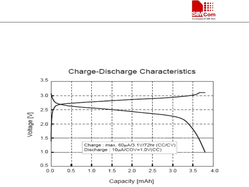
Typical charge curves for each cell type are shown in following figures. Note that the
rechargeable Lithium type coin cells are generally pre-charged from the vendor.
Figure 11: Seiko MS518 Charge and discharge Characteristic
Note:
Gold-capacitance backup
Some suitable coin cells are the electric double layer capacitors. They have a small physical
size (6.8 mm diameter) and a nominal capacity of 0.2 F to 0.3 F, giving hours of backup time.
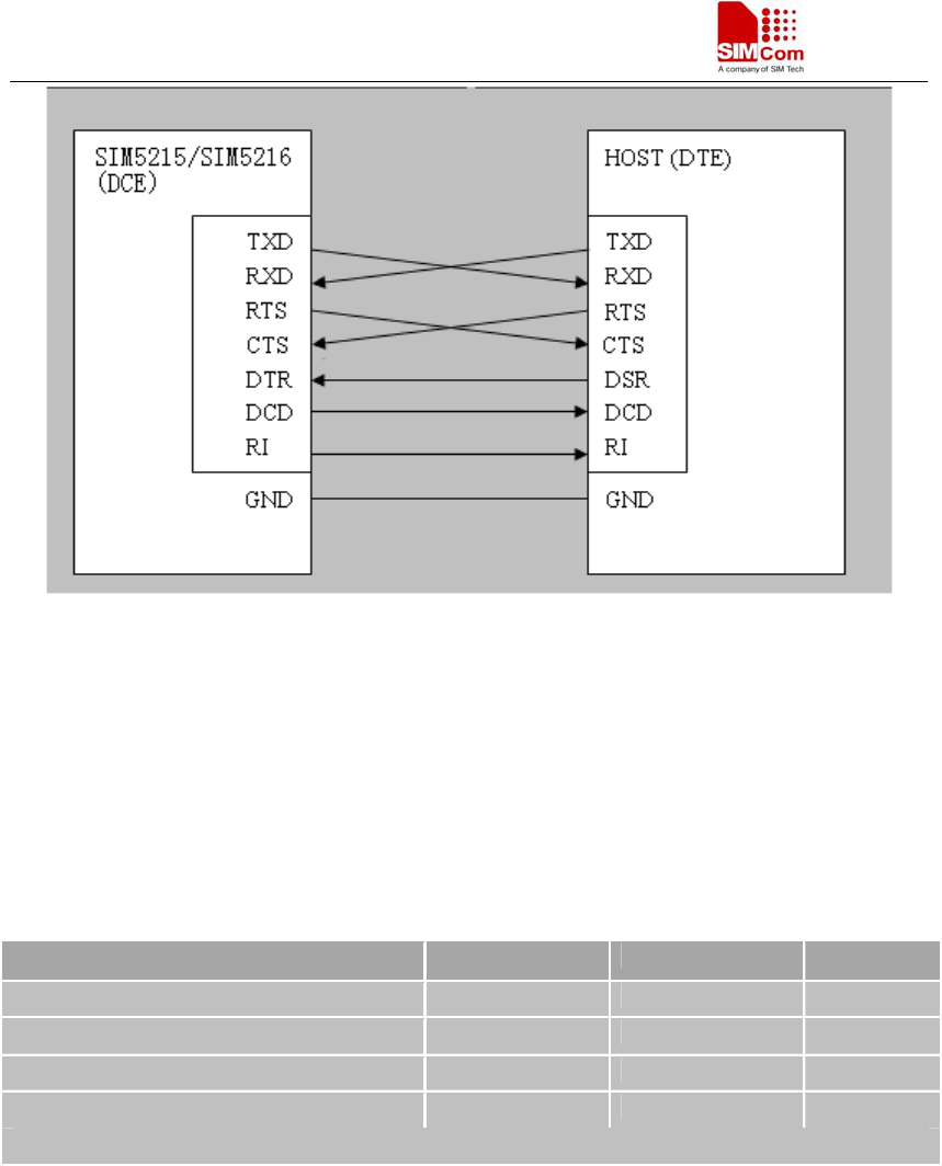
3.7 Serial interface
SIM5215A provides an unbalanced asynchronous serial port. The module is designed as a DCE
(Data Communication Equipment), following the traditional DCE-DTE (Data Terminal
Equipment) connection, the module and the client (DTE) are connected through the following
signal (as following figure shows).
SIM5215A _HD_V1.02 Hardware Design
SIM5215A _HD_V1.02 26.08.2010
27
Figure 12: Interface of serial ports
Serial port
z Port/TXD @ Client sends data to the RXD signal line of module
z Port/RXD @ Client receives data from the TXD signal line of module
All pins of all serial ports have 8mA driver, the logic levels are described in the following table
Table 8: Logic levels of serial ports pins
Parameter Min Max Unit
Logic low input 0 0.3*VDD_EXT V
Logic high input 0.7 *VDD_EXT VDD_EXT +0.3 V
Logic low output GND 0.2 V
Logic high output VDD_EXT -0.2 VDD_EXT V
Note: VDD_EXT=2.6V, is module internal IO reference voltage.
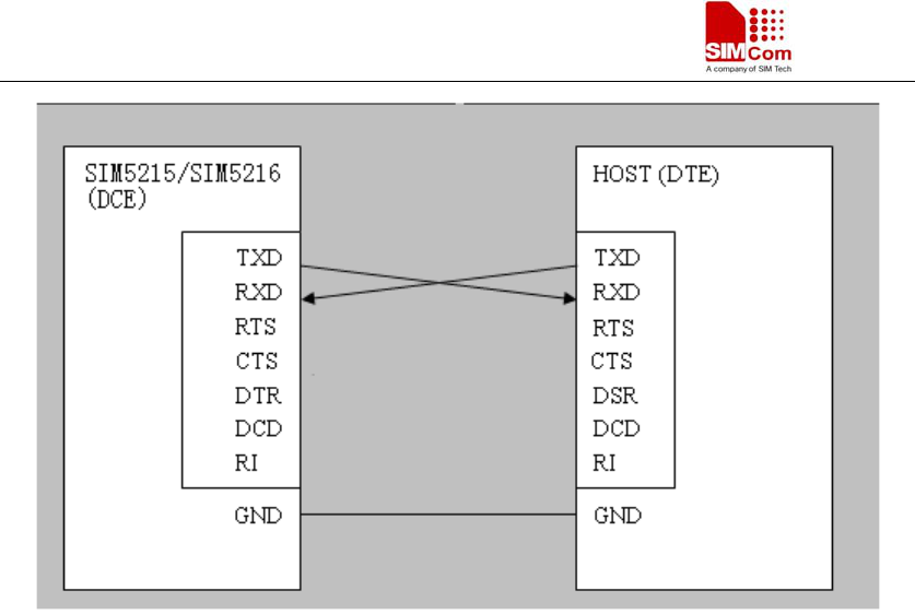
SIM5215A provides an AT command (AT+CSUART) to support Null modem. Null modem mode
uses two lines (RXD, TXD (GND not comprised)) to setup communication between devices. The
lines connection is shown as below.
SIM5215A _HD_V1.02 Hardware Design
SIM5215A _HD_V1.02 26.08.2010
28
Figure 13: Null modem mode of serial ports
If serial port is used in Null Modem, the pin “RI” can be used as an interrupt pin. Normally it
will stay high but in certain condition such as SMS receiving, incoming voice (CSD, video) call or
URC reported, the pin “RI” will be set low to inform the master, and it will stay low until the
master clear this interrupt with AT command (AT+CRIRS). If using seven lines to setup
communication between devices, the pin “RI” is different. First it stays high, when a voice (CSD)
call coming, the pin “RI” is set to low for about 5900ms, then it is set high again about 100ms.
The situation will repeat until that the call is answered or hung up. After the call is answered or
hung up, the pin “RI” is set high.
Functions of serial port supporting on SIM5215A are as following:
z Standard/Null Modem mode on Serial Port Interface.
z Contains Data lines TXD and RXD, State line RTS and CTS
z Serial Port can be used for CSD, PS service and send AT command for controlling module.
z Serial Port is a high-speed port. It supports the communication rate as following:
300, 600, 1200, 2400, 4800, 9600, 19200, 38400, 57600, 115200, 230400, 460800, 921600,
3200000, 3686400, 4000000
Default band rate is 115200bps. And Data bits=8, Parity=None, Stop bits=1, Flow
control=None.
NOTE:
1 If you need to use a speed higher than 115200, you should consider the length of RS232
line and the speed support on your RS232 port.
2 Though the connector has seven lines for serial port, but the line: DCD, DTR are not
implemented and reserved for future use.
3 The line RI behaves the same as the standard when using four-line mode, but in two-line
mode its action is not standard which is depicted above.
SIM5215A _HD_V1.02 Hardware Design
SIM5215A _HD_V1.02 26.08.2010
29
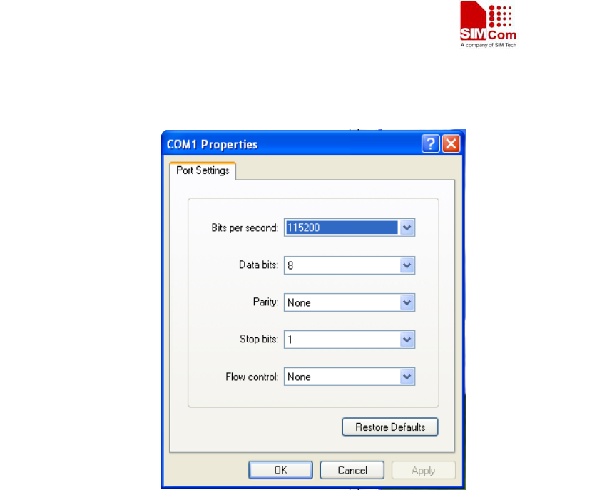
Default setting in HyperTerminal software is as the following figure.
Figure 14: Settings of serial ports
3.8 Audio interfaces
The module provides three analogy audio output channels and two analogy audio input channels.
MIC_P/N and HP_MICP, are used for microphone (two analogy audio input channels), EAR_P/N,
HPR/HPR and SPK_P/N are used for audio output (three analogy audio output channels). There
are some AT Commands to control audio channel switch and other parameters, please refer to ATC
manual.
Note: Please reference document [21] for detailed information of Audio Application Note.
Table 9: Audio interface signal
SIM5215A _HD_V1.02 Hardware Design
SIM5215A _HD_V1.02 26.08.2010
30
It is suggested that you adopt one of two following reference circuits in order to get well speaker
effect. The different audio signals have to be routed according to different signal layout rules as
in following figures:
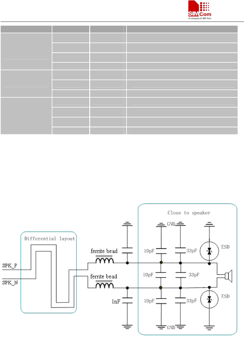
3.8.1 Speaker interface configuration
Figure 15: Speaker interface configuration
Because SPK_P and SPK_N are outputs of Class-D audio amplifier, optional EMI filtering is
shown at Figure 15; these components (two ferrite beads and two capacitors) can be added to
reduce electromagnetic interference. If used, they should be located near the SPK_P and SPK_N.
Considerable current flows between the audio output pins and the speaker, so wide PCB traces are
recommended (~ 20 mils).
Audio channel Pin name Pin No Function
MIC_P 43 MIC anode input
MIC_N 44 MIC cathode input
EAR_P 25 Receiver output anode
NORMAL
( default )
EAR_N 26 Receiver output cathode
HP_MICP 42 Headset MIC anode input
HPR 27 Headset right speaker
HEADSET
HPL 28 Headset left speaker
MIC_P 43 MIC anode input
MIC_N 44 MIC cathode input
SPK_P 23 Loudspeaker anode
Hand free
SPK_N 24 Loudspeaker cathode
SIM5215A _HD_V1.02 Hardware Design
SIM5215A _HD_V1.02 26.08.2010
31
Figure 16: Receiver interface configuration
3.8.2 Microphone interfaces configuration
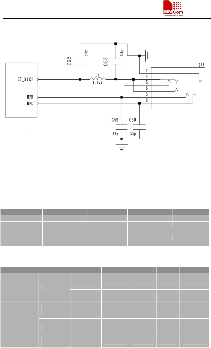
Figure 17: Microphone interface configuration
NOTE : SIM5215A has integrated internal MIC bais circuit. There is no need to pull the
MIC1_P and MIC_M up to the external power, because they have been pulled up in the Module.
MIC_P and MIC_N should be layout differential.
SIM5215A _HD_V1.02 Hardware Design
SIM5215A _HD_V1.02 26.08.2010
32
3.8.3 Earphone interface configuration
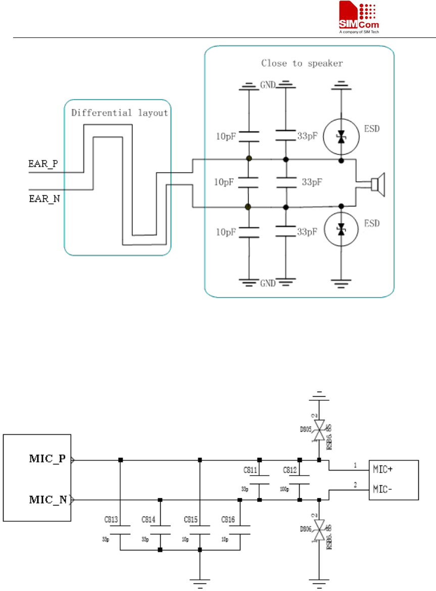
Figure 18: Earphone interface configuration
3.8.4 Referenced electronic characteristic
Table 10: MIC Input Characteristics
Parameter Min Typ Max Unit
Working Voltage 1.2 1.60 2.2 V
Working Current 70 400 uA
External
Microphone
Load Resistance
1.2 2.2 k Ohms
Table 11: Audio Output Characteristics
Parameter Min Typ Max Unit
load
Resistance 27 32 Ohm Normal
Output(EAR_P,
EAR_N)
Differential
Output
power 70 mW
Single
Ended
load
Resistance 12 16 Ohm
Differential load
Resistance 27 32 Ohm
Auxiliary
Output(HPR,H
PL)
Single
Ended
Output
power 21.6 mW

SIM5215A _HD_V1.02 Hardware Design
SIM5215A _HD_V1.02 26.08.2010
33
Table 12: Speaker Output Characteristics
Parameter Min Typ Max Unit
Quiescent
Current 6.2 mA
Output
power(1KHz) 500 mW
3.8.5 Programming characteristic
3.8.5.1 Setting Audio Parameters by AT Commands
The audio modes 1 to 3 can be temporarily adjusted according to the AT command parameters
listed in the table below. The audio parameters are set with the AT commands AT+CMICAMP1,
AT+SIDET, AT+CTXGAIN, AT+CRXGAIN, AT+CTXVOL, AT+CTXFTR, AT+CRXFTR as
we l l a s AT + CLVL ,AT +C VLVL , AT+ VM UT E , AT +M I CM UT, AT+ CS DV C, a nd AT +C PTON E.
For a model of how the parameters influence the audio signal path see Section 3.8.5.2.
Table 13: Audio parameters adjustable by AT command
Parameter Influence to Range Gain
range
Calculation AT command
micAmp1 MICP/MICN analogue
amplifier gain before ADC
0…1 0…24dB 2 steps AT+CMICAMP1
txVol Digital gain of input signal
after ADC
0,
1...65535
Mute,
-84...+12
dB
20 * log
(txVol/
16384)
AT+CTXVOL
txGain Digital gain of input signal
after summation of
sidetone
0,
1...65535
Mute,
-84...+12
dB
20 * log
(txGain/
16384)
AT+CTXGAIN
txFilter Input PCM 13-tap filter
parameters, 7 values
0...65535 --- MATLAB
calculate
AT+CTXFTR
rxGain Digital gain of output
signal after summation of
sidetone
0,
1...65535
Mute,
-84...+12
dB
20 * log
(rxGain/
16384)
AT+CRXGAIN
rxVol Digital Volume of output
signal after speech
decoder, before summation
of sidetone and DAC
-300…300 dbm -300…300d
bm
AT+CLVL
AT+CVLVL
AT+CRXVOL
stGain Digital attenuation of
sidetone
0, 1...65535 Mute,
-96...0dB
20 * log
(stGain/
16384) -12
AT+SIDET
rxFilter Output PCM 13-tap filter 0...65535 --- MATLAB AT+CRXFTR
SIM5215A _HD_V1.02 Hardware Design
SIM5215A _HD_V1.02 26.08.2010
34
parameters, 7 values calculate
NOTE: if you want to better experience on audio, you should modify these parameters for your
own electronic and mechanical design of audio part. The 13-tap filter parameter could be
debugged and calculated by MATLAB.
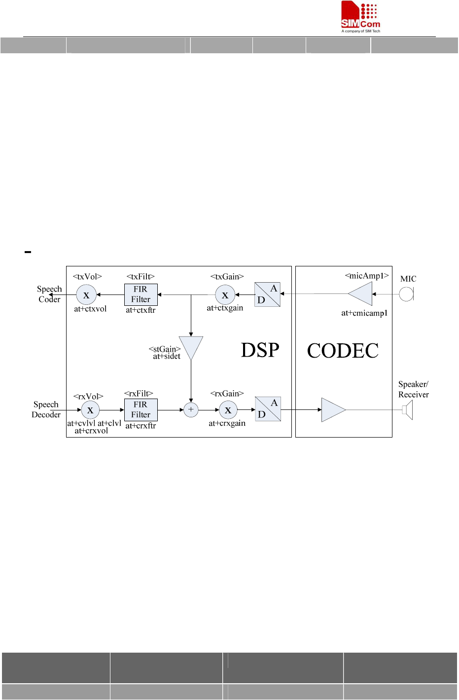
3.8.5.2 Audio Programming Model
The audio programming model shows how the signal path can be influenced by varying AT
command parameters. Parameters <micAmp>, <txGain> , <txVol>, <txFilter>,<rxGain>,
<stGain> ,<rxVol> and <rxFilter> can be adjusted with corresponding AT commands. For more
information on the AT commands and parameters see Section 3.8.5.1.
NOTE: Please reference document [1] for detailed information of each AT command.
Figure 19: Audio programming model
Note: There is no AT+CMIC in SIM5215A, because there is only one analogue hardware
amplifier which is supported by AT+CMICAMP1.
3.8.5.3 Audio characteristics
The electrical characteristics of the voice band part depend on the current audio mode (device
number) set with the AT+CSDVC command. All values are noted for default gains.
Table 14: Audio Characteristics
Audio Device no.
AT+CSDVC=
1 2 3
Name Handset Headset Speaker phone

SIM5215A _HD_V1.02 Hardware Design
SIM5215A _HD_V1.02 26.08.2010
35
Purpose Default for DSB with
Votronic handset
Mono Headset handheld speaker-phone
TX-Filters Adjustable Adjustable Adjustable
RX-Filters Adjustable
adjusted to fit artificial
ear type 3.2 low leakage
Adjustable Adjustable
500 Hz HP
Gain setting: Adjustable Adjustable Adjustable
micAmp1 0(0 dB) 0(0 dB) 0(0 dB)
txGain 23143 51811 32690
txVol 16384 16384 16384
Default
MIC path
Parameters
txFilter
[tap0~6]
0xff33, 0x05d8,
0xf488, 0x0af3,
0x24bb, 0xca42,
0x7c95
0,0,0,
0,0,0,0
0xfff3, 0x001d,
0xffb9, 0x016b,
0xfa71, 0x0c08,
0x309a
rxGain 11599 6523 41155
rxVol -100 -100 0
stGain 2304 1024 0
Default
Output
path
Parameters rxFilter
[tap0~6]
0xff00, 0xfac9,
0x0571, 0xf365,
0x0bc2, 0xf2bb,
0x533a
0,0,0,
0,0,0,0
0xfd3f, 0xfc4f,
0xfb60, 0xfa27,
0xf97c, 0xf920,
0x3934
Power supply VMIC ON during call ON during call ON during call
Sidetone Adjustable Adjustable Adjustable
Volume control Adjustable Adjustable Adjustable
Echo canceller Filter
length Behaviour
optimized for
ON 16ms low echo ON 16ms moderate echo ON 64ms high echo
Non Linear Processor
with Comfort Noise
Generator
ON ON ON
Noise Reduction -12dB -12dB -12dB
MIC input signal for
0dBm0, 1 f = 1024 Hz 17.5mV 5mV 5mV
EP output signal in mV
rms. @ 0dBm0, 1024
Hz, no load (default
gain) / @ 3.14 dBm0
508mV 2.1Vpp 407mV 1.68Vpp 1220mV 4.5Vpp
Sidetone gain at default
settings
25.0dB 25.3 dB -∞ dB

SIM5215A _HD_V1.02 Hardware Design
SIM5215A _HD_V1.02 26.08.2010
36
3.8.5.4 Adjust the sound level by AT+CVLVL
There are two adjustable amplifiers on audio signal output path: <rxVol>, <rxGain>. Four AT
commands are provided for tune them..
<rxVol>: AT+CLVL, AT+CVLVL,AT+CRXVOL
<rxGain>: AT+CRXGAIN
AT+CRXVOL is used for fine tuning for <rxVol>. AT+CLVL and AT+CVLVL are used for
coarse tuning for <rxVol>. AT+CVLVL changes the sound level values of the command CLVL.
Now we provide 5 levels for each audio channel. The level 0 is muted and it can not be changed
by CVLVL. Levels 1 to 4 are supported to change the value of sound level. CVLVL command
could let you change these four levels. The bigger the number presents the louder the voice. And
the range of each level is -5000 to 5000.
NOTE: This command influences digital volume of output signal after speech decoder. Please
check the reference document [1] for detailed information of each AT command.
3.9 USIM card interface
3.9.1 USIM card application
You can use AT Command to get information in USIM card. For more information, please refer
to document [1].
The universal subscriber identification module (USIM) is a smart card for UMTS/GSM cellular
applications. The USIM provides the required subscription information to allow the mobile
equipment to attach to a GSM or UMTS network. The USIM also provides the subscriber's
verification procedures as well as authentication methods for network authentication during the
attach procedures. The USIM card can be inserted into any UMTS/GSM USIM equipped
handset, allowing the user to receive or make calls, and receive other subscribed services from any
USIM equipped handset, thus enabling more handset independence for the user.
Both 1.8V and 3.0V SIM Cards are supported.
The SIM interface is powered from an internal regulator in the module having nominal voltage
2.8V. All pins reset as outputs driving low. Logic levels are as described in the table below.
Table 15: USIM interface
SIM5215A _HD_V1.02 Hardware Design
SIM5215A _HD_V1.02 26.08.2010
37
Table 16: Signal of USIM interface (board-to-board connector)
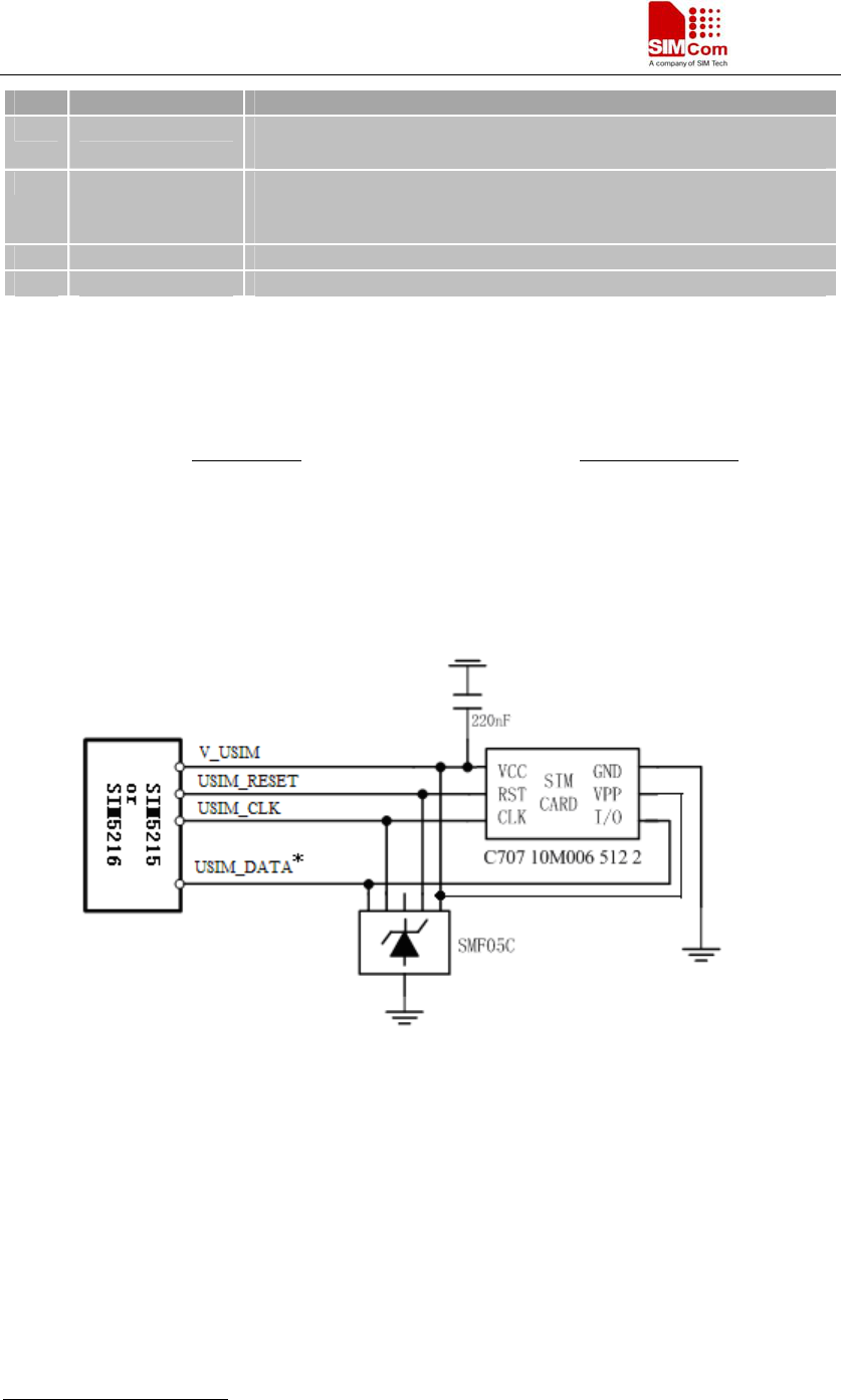
Following is the reference circuit of the USIM interface. We recommend using an Electro-Static
discharge device ST (www.st.com ) ESDA6V1W5 or ON SEMI (www.onsemi.com ) SMF05C
for “ESD ANTI”. If you remove ESD components, please replace them with 33pF and 10pF
capacitors, it’s good for EMI performance. Note that the USIM peripheral circuit close to the
USIM card socket.
You can select the 6 pins USIM card. The reference circuit about 6 pins USIM card illustrates as
in the following figure.
Figure 20: USIM interface reference circuit with 6 pins USIM card
*Note: USIM_DATA has been pulled up with a 22kR resistor to V_USIM in module. So
please do not pull up or pull down in your application circuit. As shown in above figure,
SMF05C is used for ESD protection for SIM interface. And 220nF capacitor on V_USIM is
used to reduce interference
3.9.2 Design considerations for USIM card holder
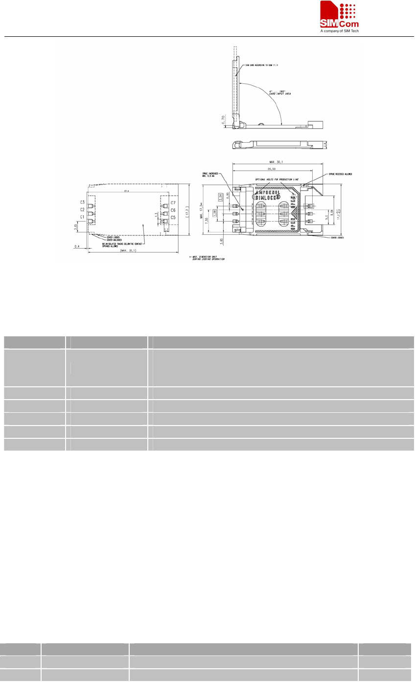
For 6 pins USIM card, we recommend to use Amphenol C707 10M006 512 2. You can visit
http://www.amphenol.com for more information about the holder.
Pin Signal Description
57 V_USIM USIM Card Power output depends automatically on USIM mode,
one is 3.0V±10%, another is 1.8V±10%. Current is about 10mA.
56 USIM_DATA USIM Card data I/O, which has been pulled up with a 22kR
resistor to V_USIM in module. So please do not pull up or pull
down in your application circuit.
12 USIM_CLK USIM Card Clock
13 USIM_RESET USIM Card Reset
SIM5215A _HD_V1.02 Hardware Design
SIM5215A _HD_V1.02 26.08.2010
38
Figure 21: Amphenol C707 10M006 512 2 SIM card holder
Table 17: Pin description (Amphenol SIM card holder)
Pin Signal Description
C1 USIM_VDD
SIM Card Power supply, it can identify automatically the SIM
Card power mode,one is 3.0V±10%, another is 1.8V±10%.
Current is about 10mA.
C2 USIM_RST SIM Card Reset.
C3 USIM_CLK SIM Card Clock.
C5 GND Connect to GND.
C6 VPP Connect to USIM_VDD
C7 USIM_DATA SIM Card data I/O.
3.10 I2C interface
SIM5215A contains an I2C interface.It is used for connecting peripheral equipment. Use AT
Command to read/write values of I2C peripheral equipment. AT+CRIIC is used for read
values from register of I2C peripheral equipment. AT+CWIIC is used for write values to register
of I2C peripheral equipment
Because I2C has been pulled up in SIM5215A, there is no need
to be pulled up by customer.
Table 18: PIN define of IIC interface
*Note
:
IIC_SDA and IIC_SCL have been pulled up with two 2.2kR resistors to 2.6V in module.
So there is no need to pull them up in your application circuit.
Pin Name Function Lever
47 IIC_SDA Serial interface data input and output
46 IIC_SCL Serial interface clock input
SIM5215A _HD_V1.02 Hardware Design
SIM5215A _HD_V1.02 26.08.2010
39
3.11 USB interface
SIM5215A supports high and full speed universal serial bus (USB) interface, and mode of USB
can be switched by AT command ( AT+CUSBSPD ) This interface is compliant with the USB 2.0
specification. The high speed is up to 480Mbps. so please pay attention to influence of junction
capacitance of ESD component on USB data lines. Typically, the capacitance value should be
less than 4pF @1MHz.
Links to these and related specifications can be found at www.usb.org
Table 19: USB PIN connect
Input voltage scope( V )
Name PIN( B to B) Min Type Max
USB_VBUS 9 4.4 5.0 5.25
USB_DP 60
USB_DM 59 They are compliant with the USB 2.0 specification.
GND 58
VBUS
D+
GND
D-
VBUS
D+
D-
GND
Series
A , B
or
Mini-B
Receptacle
Figure 22: USB interface
Currently SIM5215A supports the USB suspend & resume mechanism which can help to save
much current. If no transaction on USB bus then SIM5215A will enter to suspend mode and
when some events happens (such as incoming call or SMS received) during the suspend mode
then SIM5215A will resume automatically.
Note: when use the Mini-B it has no ID line.
Note
:
Two limitations on ESD protection: less than 4 pF and VBUS not to rail.
SIM5215A _HD_V1.02 Hardware Design
SIM5215A _HD_V1.02 26.08.2010
40
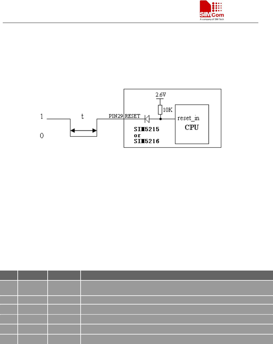
3.12 Module Reset
SIM5215A also have a RESET pin (PIN29) input, When should reset the module, one can push
the RESET pin to low and the module reset. Because the Reset pin has been pulled up in
SIM5215A, there is no need to pull it up in application circuit. The internal circuit about RESET
pin is shown below.
NOTE
:
50ms<t<200ms.
In order to improve the ESD of Reset pin, the bidirectional ESD component is suggested to be
used on Reset pin.
NOTE: In automatically powering on mode, it is suggested that the SIM5215A should reset by
RESET pin after power on.
3.13 General purpose input & output (GPIO)
SIM5215A provides a limited number of General Purpose Input/Output signal pin. Please check
the following table:
Table 20: GPIO Pins of SIM5215A
GPIO0 is used for interrupt pin, default triggering mechanism is level trigger, and low level
will trigger interrupt. After interrupt, SIM5215A would send out Alarm information to host
CPU. Please Refer to “AT Command Manual”.
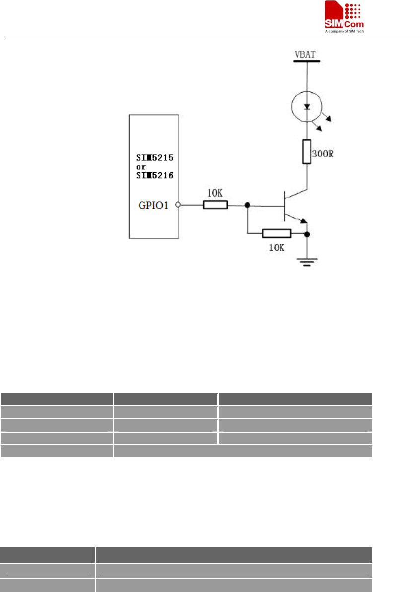
GPIO1 is used to control Status LED, the LED driving circuit of GPIO1 is shown below, and
status table is Table 23.
Pin Name Direction Function
65 GPIO0 Input,
interrupt
Input Port with interrupt/PCM_DIN
Use AT Command to set interrupt triggering mechanism & polarity .
10 GPIO1 Output used as status LED driver
30 GPIO2 Input General Purpose Input Port without interrupt/PCM_SYNC
31 GPIO3 Output General Purpose Output Port (default value: Low Level)/PCM_CLK
32 GPIO4 Input RF Control Interrupt:Flight Mode Switch
33 GPIO5 Output General Purpose Output Port (default value: Low Level)/PCM_DOUT
SIM5215A _HD_V1.02 Hardware Design
SIM5215A _HD_V1.02 26.08.2010
41
Figure 23: status LED circuit
Notes: 300R Resistor’s value depends on LED.
And status indicating table is as follow.
Table 21:meanings of status LED
Status Data Voice
Always On Searching Network Searching Network/Call Connect
200ms ON, 200ms OFF Data Transmit
800ms ON, 800ms OFF Registered network Registered Network
Off Power Off
GPIO4 can be used to control RF close or on, the Flight Mode Switch logic table is shown
below. You can use AT Command to read or to write GPIO2, GPIO3, GPIO5 status (High or Low
level).
Table 22:Logic of GPIO4
Use AT Command to read or write GPIO2, GPIO3, GPIO5 status (High or Low level).
NOTE
:
For SIM5215A, GPIO0, GPIO2, GPIO3 and GPIO5 can be multiplex function, you
can use them as PCM interface to connect extend codec. Please refer section 3.18 and
document [1] for detail information.
GPIO4 Status Module Action
L Flight Mode: RF is closed.
H Normal Mode: RF is working.
SIM5215A _HD_V1.02 Hardware Design
SIM5215A _HD_V1.02 26.08.2010
42
3.14 ADC interface
SIM5215A has an analog-to-digital converter (ADC) that is available for digitizing analog signals
such as battery voltage, temperature and so on, it is on PIN 30, namely HKADC0, This HKADC0
is 8 bit successive-approximation circuit, and performance specification is shown in the following
table:
Table 23:ADC Characteristics
Specification Min Typ Max Unit Comments/Conditions
Resolution 8 Bits
differential
nonlinearity
-4 +4 LSB
Integral nonlinearity -8 +8 LSB
Gain Error -2.5 +2.5 %
Offset Error -4 +40 LSB
. Analog Vdd = ADC reference
300 kHz - 1.2 MHz sample rate
Input Range GND 2.2 V
3dB input
bandwidth
2500 Source resistance = 50 Ω
Input serial
resistance
2 kΩ Sample and hold switch resistance
Input capacitance 53 pF
Power-down to
wakeup
9.6 19.2 μs
One can introduce a signal into this ADC pin directly and use AT+CADC to get the raw data value
between 0 and 255 which can then be transformed to any other type such as voltage, temperature
etc.
Note: if the signal is voltage then the voltage value must no more than 2.2V.
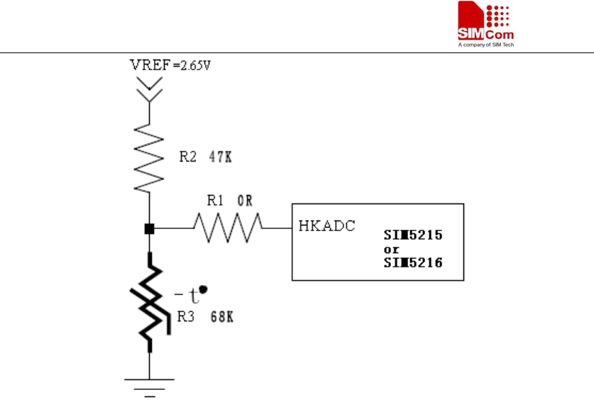
Show an application sample:
You can use it as a temperature ADC channel, too. The reference design of a temperature ADC
circuit is as the figure below. R1 is 0Ω, R2 is 47 kΩ and R3 is 68 kΩ for reference. ,,the return
value is supposed to 158 by AT+CADC, and you can use some arithmetic to translate “158” to a
specifically temperature.
SIM5215A _HD_V1.02 Hardware Design
SIM5215A _HD_V1.02 26.08.2010
43
Figure 24:ADC interface used for temperature sampling reference circuit
3.15 LDO power output
SIM5215A has a LDO power output, it is PIN 40, namely VREG_AUX. This LDO default
output voltage is 2.85V, and the driver current is rated for 250mA. This LDO could be used as a
power supply for SD card, and the SD card data/command lines can also been pulled up by it. One
can switch the LDO by AT+CVAUXS also one can set the LDO’s output voltage by
AT+CVAUXV.
NOTE
:
SIM5210 has no such pin. This is a difference between SIM5215A and SIM5210.
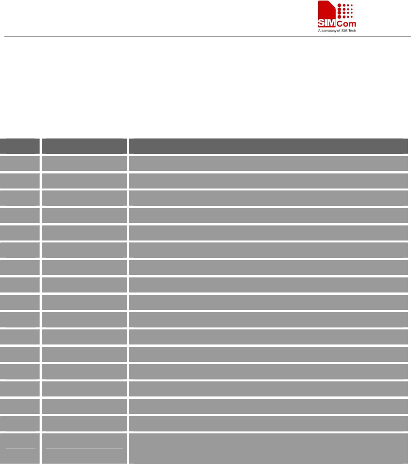
3.16 Camera module interface
SIM5215A provides a camera module interface for supporting camera and video phone functions.
If you do not use the camera interface, you can configure these pins as configurable GPIOs. Please
refer the AT command Document (AT+CCGSWT).
SIM5215A support both digital and analog sensor (NTSC or PAL composite signals output), YUV
and RGB data format. When using analog sensor, you need to use AK8856 (currently we
supported) to decode NTSC or PAL composite signals into digital data first and then transmit the
digital data into camera interface.
Note: When you use a YUV output sensor, you should connect the sensor data output
pin(OV7670 : data0~data7; OV2640 and OV7725 : data2~data9) to SIM5215A
CAM_D2~CAM_D9.
The camera module interface consists of the following:
SIM5215A _HD_V1.02 Hardware Design
SIM5215A _HD_V1.02 26.08.2010
44
■ 8 bit data bus for the pixel data information
■ Horizontal and vertical synchronization signals
■ 2 wire I2C bus as a control path between the SIM5215A module device and the camera module
The following table is the pin definition.
Table 24: PIN define of sensor interface
We have tested several kinds of digital sensors, such as OV2640, OV7670,OV7725 and a
NTSC/PAL digital video decoder named AK8856 (it can decode NTSC or PAL composite video
signals into digital video data, and with AK8856 you can use analog sensor as video source) .
Software must be adjusted when use other kinds of sensors. Customer can contact us and give us
your request. The power supply of the sensor should be supplied by customer.
Pin Name Function
15 CAM_D2 Bit 0 of RGB or YUV D0 video component output
54 CAM_D3 Bit 1 of RGB or YUV D1 video component output
16 CAM_D4 Bit 2 of RGB or YUV D2 video component output
53 CAM_D5 Bit 3 of RGB or YUV D3 video component output
17 CAM_D6 Bit 4 of RGB or YUV D4 video component output
52 CAM_D7 Bit 5 of RGB or YUV D5 video component output
18 CAM_D8 Bit 6 of RGB or YUV D6 video component output
51 CAM_D9 Bit 7 of RGB or YUV D7 video component output
19 CAM_HSYNC Video horizontal line synchronization signal
50 CAM_VSYNC Vertical sync output
21 CAM_CLK master clock input
49 CAM_PCLK Pixel clock output
48 CAM_RESET Master reset input, active low
47 IIC_SDA Serial interface data input and output
46 IIC_SCL Serial interface clock input
20 GND Ground
22 CAM_STANDBY Power-down mode selection
“0”=Normal mode, “1”=Power-down mode
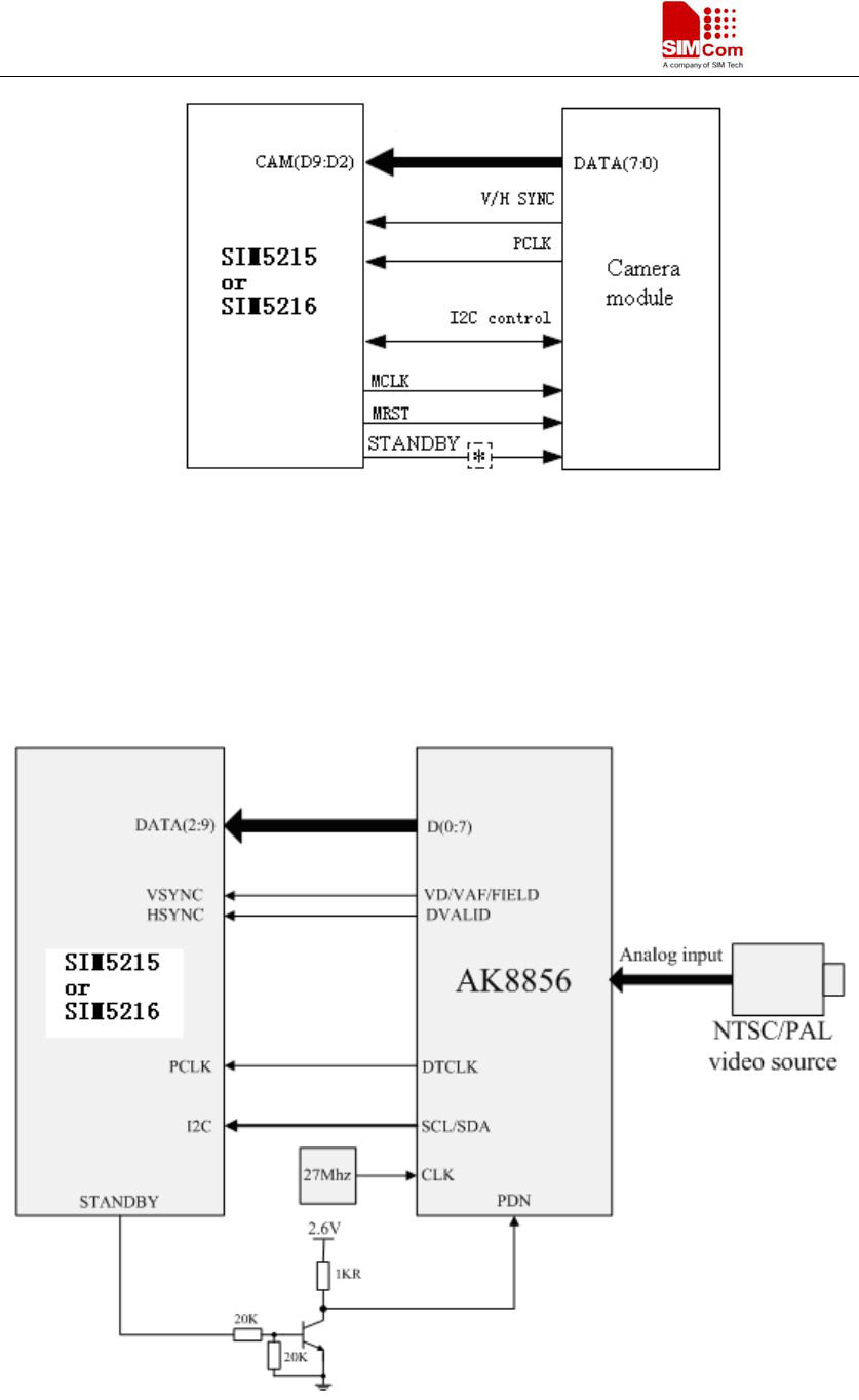
SIM5215A _HD_V1.02 Hardware Design
SIM5215A _HD_V1.02 26.08.2010
45
Figure 25: Camera module interface
NOTE
:
The data and clock lines of camera are sensitive for the capacitors. Generally the
capacitance of the ESD component is too big, if those ESD components are put on to the
parallel line then the signal will fade a lot. In order to improve the ESD performance, some
10pF capacitor can be put on data and clock lines for ESD. If one like to choose smaller
capacitance ESD component, it should be smaller than 10pF.
Figure 26: Camera module interface with analog sensor

SIM5215A _HD_V1.02 Hardware Design
SIM5215A _HD_V1.02 26.08.2010
46
*NOTE
:
STANDBY pin of SIM5215A is used to control the powering down or on of camera
module. So when one designs application circuit, one should pay attention to the polarity of
STANDBY. Default polarity of SIM5215A is shown below:
LOW: normal operation
HIGH: power-down
In Figure 26, the polarity of AK8856 power down is contrary to that of SIM5215A STANDBY,
so one must use a NPN triode to reverse the polarity of SIM5215A and connect AK8856.
If you do not use the camera interface you can configure these pins to configurable GPIOs.
Please refer the AT command Document (AT+CCGSWT).
3.17 MMC/SD card interface
SIM5215A provides one MMC/SD card interface. The SIM5215A acts as a HOST. The
SIM5215A device has a 4-bit SD interface. It supports 4 bits of data and a command signal. In
addition, a clock output is provided by the SIM5215A to be used as SD_CLK, or MMC_CLK.
This clock is designed to be used with the MMC/SD interface and is what customers should use
with the MMC/SD cards. A LDO power output is provided by the SIM5215A for the power
supply of MMC/SD card, it is PIN 40, name VREG_AUX. This LDO default output voltage is
2.85V, and driver current is rated for 250mA. Meanwhile data lines can be pulled up by
VREG_AUX. The reference circuit of MMC/SD card interface is shown in Figure 27. The 10KR
pull-up resistors on data and clk lines are necessary. The 33pF capacitor is used to reduce RF
interference. To get good ESD performance, some ESD components should be added beside the
SD/MMC card holder.
The following features are implemented:
■ Supports 4-bit SD, 1-bit SD, and 1-bit MMC interface
■ SW-configurable edge latching (falling or rising)
■ SW-configurable data and command values change (rising or falling edge)
■ Clock-gating for power saving (and a power-saving option to always turn the clock off
when bus is idle)
■ Flow control option to prevent overflow and underflow
■ SD_CLK output up to 50 MHz
Following figure illustrate and describe the MMC/SD interface.
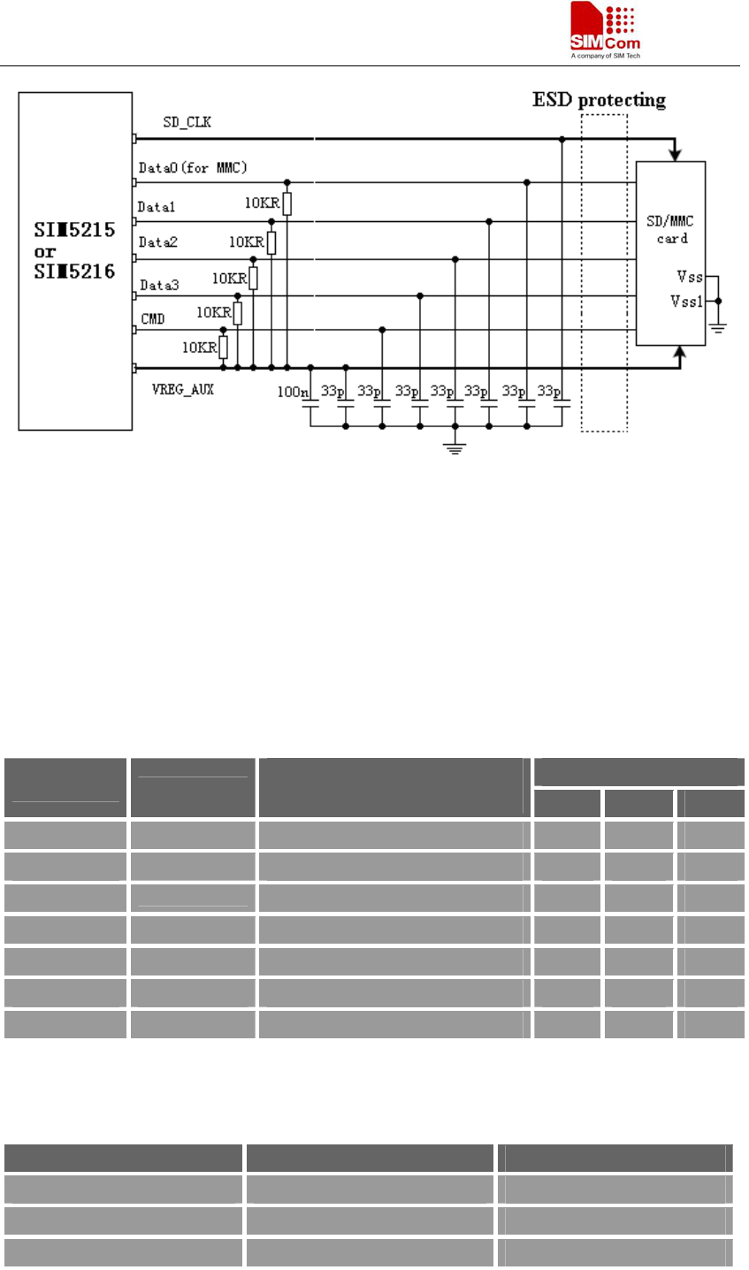
SIM5215A _HD_V1.02 Hardware Design
SIM5215A _HD_V1.02 26.08.2010
47
Figure 27: MMC/SD interface
As mentioned, the MMC/SD interface supports SD according to the SD physical layer
specification 2.0, up to 4-bit data mode. It is also capable of supporting 1-bit MMC according to
MCC specification 3.31. While the same hardware controller is used, the initialization for SD
cards and MMCs are different. SIM5215A will auto-detect which card is inserted (SD or MMC,
or no card) and will proceed accordingly.
Table 25: MMC/SD pin of SIM5215A
voltage scope( V )
Name Direction Pin
On board-to-board connector Min Type Max
SD_DATA0 Input /Output 36 2.7 2.85 3.0
SD_DATA1 Input /Output 37 2.7 2.85 3.0
SD_DATA2 Input /Output 38 2.7 2.85 3.0
SD_DATA3 Input /Output 39 2.7 2.85 3.0
SD_CLK Output 34 2.7 2.85 3.0
SD_CMD Output 35 2.7 2.85 3.0
VREG_AUX Output 40 2.7 2.85 3.0
Table 26 : MMC/SD pin connector
Name SD card MMC card
SD_DATA0 SD_DATA0 MMC_data
SD_DATA1 SD_DATA1 NC
SD_DATA2 SD_DATA2 NC

SIM5215A _HD_V1.02 Hardware Design
SIM5215A _HD_V1.02 26.08.2010
48
SD_DATA3 SD_DATA3 NC
SD_CLK SD_CLK MMC_CLK
SD_CMD SD_CMD MMC_CMD
VREG_AUX SD_VDD MMC_VDD
Note
:
SD card interface function is supported by SIM5215A software. You can use
VREG_AUX for power supply of SD card and as the pull up power for data lines.
3.18 PCM Interface
SIM5215A provides hardware PCM interface for external codec. PCM interface pins are
multiplex on GPIOs(default setting). Use AT+CPCM command to change pins function between
PCM function and GPIOs.If enbale PCM function ,AT+CPCM command can be used to configure
the PCM mode user want. Also the slot of PCM can be configured by AT+CPCMSLOT.
SIM5215A PCM interface can be used in two modes:
1) the default mode is its auxiliary PCM (8 kHz long sync mode at 128kHz clk);
2) the other mode is its primary PCM (8 kHz short sync mode at 2048 kHz clk).
In short-sync (primary PCM) mode, the SIM5215A can be a master or a slave. In long-sync
(auxiliary PCM) mode, the SIM5215A is always a master; there is no slave support.
SIM5215A support 3 PCM formats: 8 bits (υ-law or A-law) and 16 bits (linear).
The PCM interface is a 4 pin, digital interface that enables PCM communication between the
Module and an external codec or DSP. Both the PCM interface modes, auxiliary and primary, use
the same SIM5215A pins. The PCM pin assignment is shown in the table below.
Note: Please reference document [22] for detailed information of PCM Application Note.
Table 27 : PCM pin assignment
Pins Pin
No.
AUX_PCM
functionality
Primary_PCM
functionality
Description
PCM_CLK/GPIO3 31 AUX_PCM_CLK PCM_CLK PCM clock for PCM
communication to
external codec
PCM_SYNC/GPIO2 30 AUX_PCM_SYNC PCM_SYNC PCM data strobe for
PCM
communication to
PCM
mode
SYNC CLK MODE Format Slot
Auxiliary 8KHz 128KHz Master Only slot 0
Primary 8KHz 2.048MHz Slave/Master
A-law(8 bits)
υ-law(8bits)
linear(16 bits) 0~15(Changed by
AT command:
at+cpcmslot)
Default:slot 0

SIM5215A _HD_V1.02 Hardware Design
SIM5215A _HD_V1.02 26.08.2010
49
external codec
PCM_DIN/GPIO0 65 AUX_PCM_DIN PCM_DIN PCM data input to
the Module (Rx)
PCM_DOUT/GPIO5 33 AUX_PCM_DOUT PCM_DOUT PCM data output
from the Module
(Tx)
The default PCM interface on power up is the auxiliary PCM interface. Under PCM, the
data is output on the rising edge of PCM_CLK and sampled at the falling edge of PCM_CLK.
Primary PCM is disabled at power up or when RESET is asserted, but you can use AT
command to enable the primary PCM mode.
PCM Interface can be operated in Master and Slave mode. When the PCM interface is
configured, PCM Tx data will be routed from the external codec Mic through the DSP encode path
in the Module. PCM Rx data will be routed through the DSP decode path to the external codec
speaker. When using the PCM Interface, the Module can be set either into Master Mode or Slave
Mode.
In Master Mode, the Module drives the clock and sync signals that are sent out to the external
codec via the PCM Interface. When in Slave Mode, the external codec drives the clock and sync
signals that are sent to the Module.
Configuration Mode can be selected either primary or auxiliary. Primary configuration mode
uses 2.048MHz clock and 8 kHz short sync clock, and auxiliary configuration mode uses 128KHz
clock and 8 kHz long sync clock. One important consideration is that Slave mode is only
available for use with Primary configuration Mode. PCM formats can also be chosen by AT
command.
In the default configuration, Module is the Auxiliary Master.
Many parameters of external codec audio channel are not available. Only RxVolume, FIR, are
still available after enabling PCM.
Table 30: PCM external codec Characteristics
Audio Device no.
AT+CSDVC=
4
Name External Codec
micAmp No available
txGain No available
txVol No available
Default
MIC path
Parameters
txFilter
[tap0~6]
0xff33, 0x05d8,0xf488, 0x0af3,
0x24bb, 0xca42,0x7c95
rxGain No available
rxVol -100
stGain No available
Default
Output
path
Parameters rxFilter
[tap0~6]
0xff00, 0xfac9,0x0571, 0xf365,
0x0bc2, 0xf2bb,0x533a
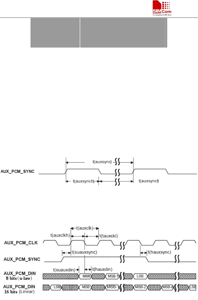
SIM5215A _HD_V1.02 Hardware Design
SIM5215A _HD_V1.02 26.08.2010
50
Default values of
sound level
(level 1 to 4)
0
0
0
0
NOTE: Please check the reference document [1] for detailed information of each AT command.
Both PCM modes are discussed in this section, followed by additional PCM topics.
3.18.1 Auxiliary PCM (128 kHz PCM clock)
The auxiliary PCM interface enables communication with an external codec to support
hands-free applications. υ-law codec are supported by the auxiliary PCM interface.
The auxiliary codec port operates with standard long-sync timing and a 128 kHz clock. The
AUX_PCM_SYNC runs at 8 kHz with 50% duty cycle. Most υ-law codec support the 128
kHz clock.
Figure 28:AUX_PCM_SYNC timing
Figure 29:EXT_CODEC to SIM5215A timing
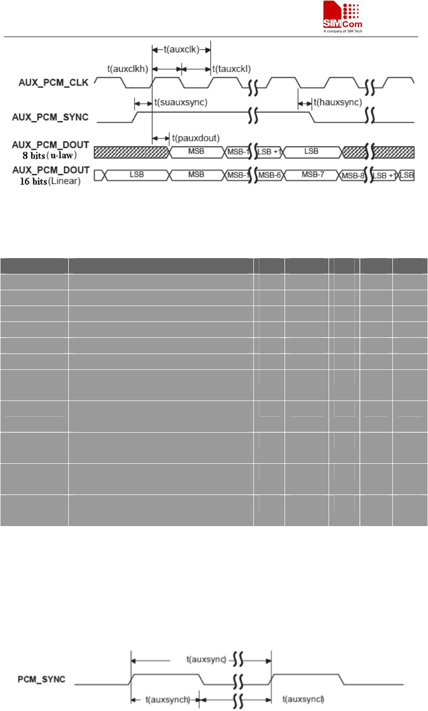
SIM5215A _HD_V1.02 Hardware Design
SIM5215A _HD_V1.02 26.08.2010
51
Figure 30:SIM5215A to EXT_CODEC timing
Table 31 : Auxiliary PCM mode timing parameters
Parameter Description Min Typical Max Unit Note
T(auxsync) AUX_PCM_SYNC cycle time – 125 - μs
T(auxsynch) AUX_PCM_SYNC high time 62.4 62.5 - μs
T(auxsyncl) AUX_PCM_SYNC low time 62.4 62.5 - μs
T(auxclk) AUX_PCM_CLK cycle time - 7.8 – μs *
T(auxclkh) AUX_PCM_CLK high time 3.8 3.9 – μs
T(auxclkl) AUX_PCM_CLK low time 3.8 3.9 – μs
T(suauxsync) AUX_PCM_SYNC setup time high
before falling edge of PCM_CLK
1.95 – – μs
T(hauxsync) AUX_PCM SYNC hold time after falling
edge of PCM_CLK
1.95 – – μs
T(suauxdin) AUX_PCM_DIN setup time before
falling edge of AUX_PCM_CLK
70 – – ns
T(hauxdin) AUX_PCM_DIN hold time after falling
edge of AUX_PCM_CLK
20 – – ns
T(pauxdout) Delay from AUX_PCM_CLK rising to
AUX_PCM_DOUT valid
– – 50 ns
*Note: t(auxclk) = 1/(128 kHz).
3.18.2 Primary PCM (2048 kHz PCM clock)
The aux codec port also supports 2.048 MHz PCM data and sync timing for υ-law codec that
matches the sync timing — this is called the primary PCM interface (or just PCM interface).
You can use AT+CPCM command to change the mode you want.
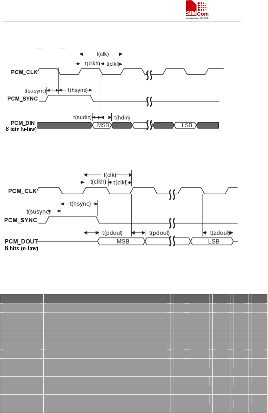
SIM5215A _HD_V1.02 Hardware Design
SIM5215A _HD_V1.02 26.08.2010
52
Figure 31:PRIM_PCM_SYNC timing
Figure 32:EXT_CODEC to SIM5215A timing
Figure 33:SIM5215A to EXT_CODEC timing
Table 32 : Primary PCM mode timing parameters
Parameter Description Min Typical Max Unit Note
T(sync) PCM_SYNC cycle time – 125 – μs
T(synch) PCM_SYNC high time 400 500 – ns
T(syncl) PCM_SYNC low time – 124.5 – μs
T(clk) PCM_CLK cycle time – 488 – ns
T(clkh) PCM_CLK high time – 244 – ns
T(clkl) PCM_CLK low time – 244 – ns
T(susync) PCM_SYNC setup time high before falling edge
of PCM_CLK
60 – – ns
T(hsync) PCM_SYNC hold time after falling edge of
PCM_CLK
60 – – ns
T(sudin) PCM_DIN setup time before falling edge of
PCM_CLK
50 – – ns
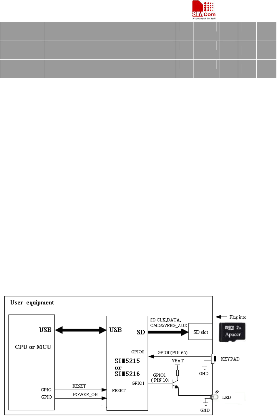
SIM5215A _HD_V1.02 Hardware Design
SIM5215A _HD_V1.02 26.08.2010
53
T(hdin) PCM_DIN hold time after falling edge of
PCM_CLK
10 – – ns
T(pdout) Delay from PCM_CLK rising to PCM_DOUT
valid
– – 350 ns
T(zdout) Delay from PCM_CLK falling to PCM_DOUT
HIGH-Z
– 160 – ns
3.18.3 Transmitting PCM data by USB
Not only by hardware PCM interface, but also SIM5215A can transmit PCM data by USB.
To transmit PCM data by USB, one should make sure that driver of SIM5215A has be loaded on
host part. Then the NEMA port of SIM5215A can be recognized by host. One can switch it from
NEMA port mode to data mode or from data mode to NEMA port mode by AT+DSWITCH. In
data mode, one can control sending and receiving PCM data by AT+CPCMREG.
Note: For 5213/5214/5215/5216, NEMA port is used to transmit PCM data.Please reference
document [22] for detailed information of PCM Application Note.
3.19 Firmware update
If SIM5215A modules are embed into user’s equipment and can’t be taken out easily, modules
provide two firmware update methods that called SD card update and USB interface update.
3.19.1 SD Card update
SD card update means that user can use SD card which the new firmware has been put in the
SIM5215A modules to update the old Firmware .
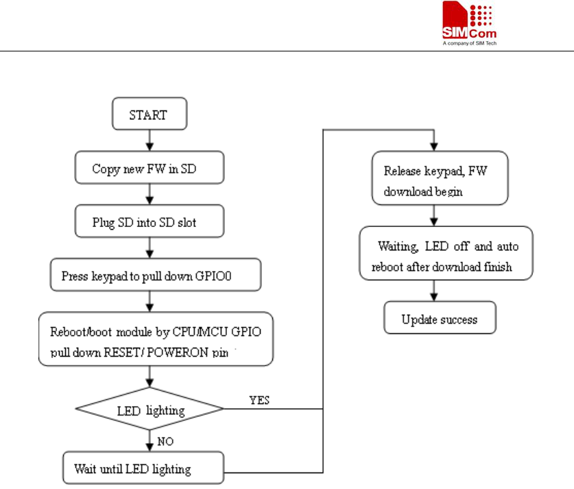
SIM5215A _HD_V1.02 Hardware Design
SIM5215A _HD_V1.02 26.08.2010
54
Figure 34:SD card update reference circuit
Figure 35:SD card update procedure
Note1: Firmware contains
:
Amss.mbn, dbl.mbn, osbl.mbn, fsbl.mbn, partition.mbn,
NPRG6270.hex, ENPRG6270.hex.
Note2: Pulling down GPIO0 when SIMcom module is booting up, is to enable the SD Card
Update function.
Note3: The status LED(GPIO1) indicates that the update is going on when booting.
Note4: This update function does not support QCN. So if the flash in the modules will be erased,
please do backup QCN by QDL at first.
Note5: This function is supported by the version 1575B04V01SIM5215A and later version.
Note6: Modules in user equipment must connect a SD slot.
Note7: Modules GPIO0 can be controlled by a GPIO on CPU/MCU, and must be pulled up
after the status LED lighting . This connecting may conflict with PCM function because
GPIO0 is multiplexed as the PCM_DIN.
3.19.2 USB interface update.
If SIM5215A communicate with MCU/CPU by hardware UART interface, user can route module
USB to a USB-A/USB-B/mini-B slot, and connect USB slot to PC with USB cable .Figure 36 is
the reference circuit.
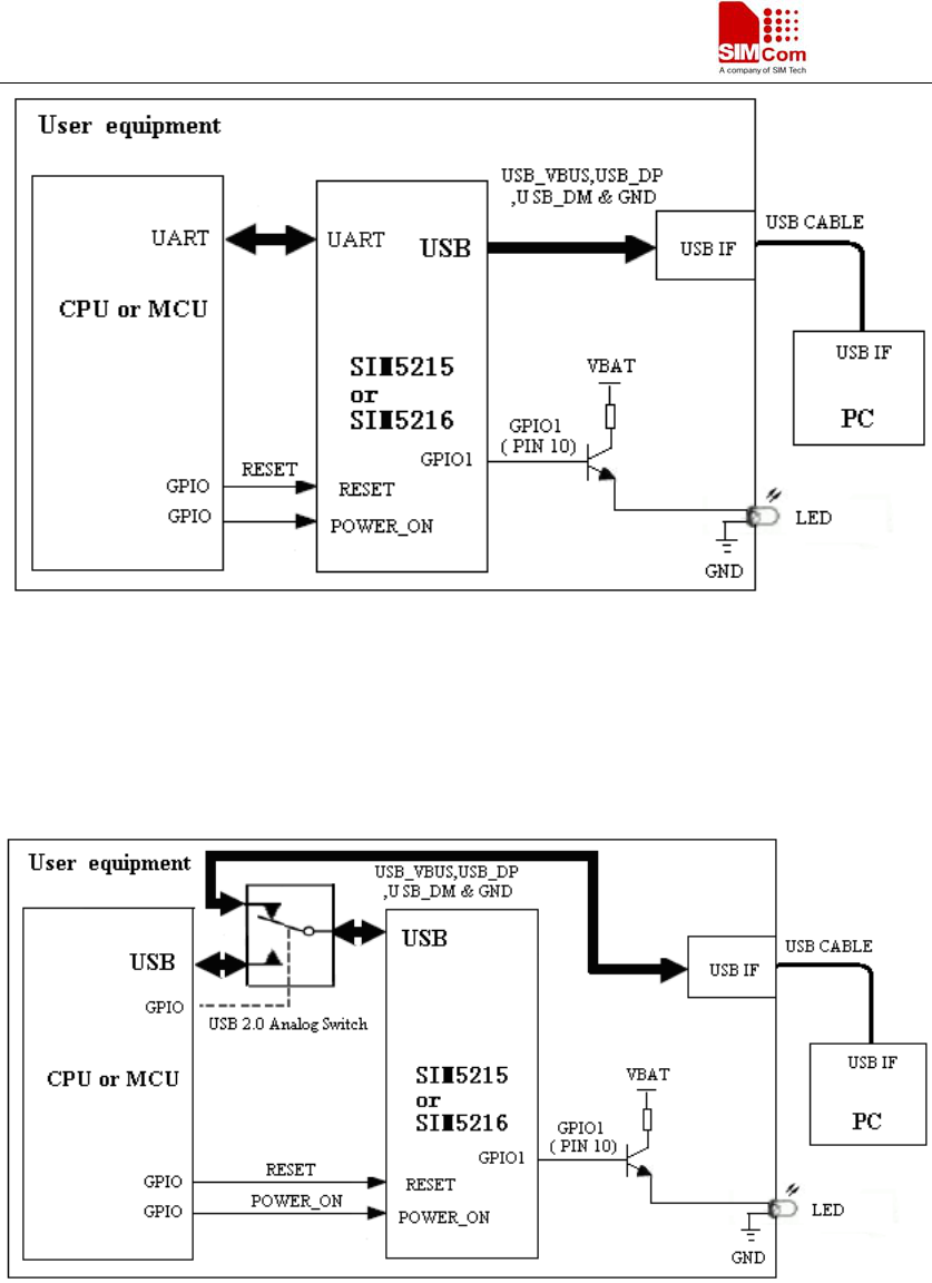
SIM5215A _HD_V1.02 Hardware Design
SIM5215A _HD_V1.02 26.08.2010
55
Figure 36:USB interface update reference circuit (UART communicate)
MCU/CPU works with SIM5215A USB interface. User can select a USB 2.0 analog switch if one
wants to use USB update. Figure 37 is the reference circuit. In USB update mode, modules are
connected to PC on USB cable by CPU/MCU GPIO controlling. For USB 2.0 analog switch, User
can use ON Semiconductor NLAS7222C.
Figure 37:USB interface update reference circuit (USB DPDT switch)
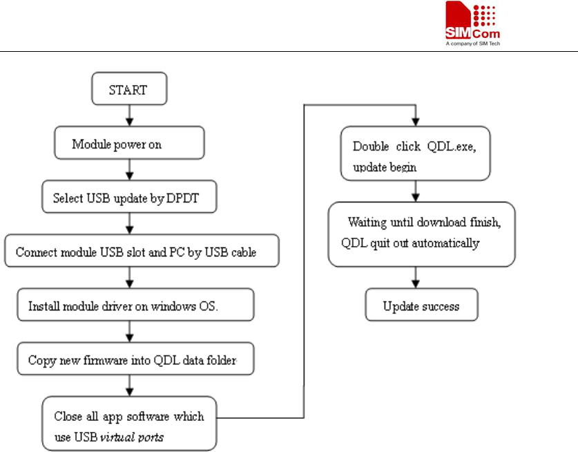
SIM5215A _HD_V1.02 Hardware Design
SIM5215A _HD_V1.02 26.08.2010
56
Figure 38:USB interface update procedure
Note1: USB 2.0 analog switch chip may add cost.
Note2: If MCU/CPU works with SIM5215A USB interface we recommend to use SD Card
update
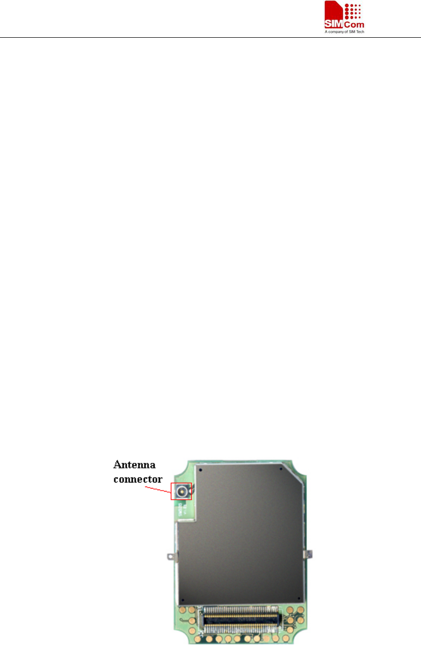
SIM5215A _HD_V1.02 Hardware Design
SIM5215A _HD_V1.02 26.08.2010
57
4 Antenna interface
The RF interface has an impedance of 50Ω. To suit the physical design of individual applications
SIM5215A offers two alternatives:
z Recommended approach: antenna connector on the component side of the PCB
z Antenna pad and grounding plane placed on the bottom side.
To minimize the loss on the RF cable, it needs to be very careful to choose RF cable. We
recommend that the insertion loss should meet the following requirements:
z GSM900/GSM850 <1 dB
z DCS1800/PCS1900 <1.5 dB
z WCDMA 1900 <1.5 dB
z WCDMA 850 <1 dB
4.1 Antenna installation
4.1.1 Antenna connector
SIM5215A use MURATA MM9329-2700 RF connector on the module side, we recommend that
user uses MURATA MXTK88XXXXX as matching connector on the application side. Please
refer to appendix for detailed information about MURATA MXTK88XXXXX.
Figure 39: Antenna Connector
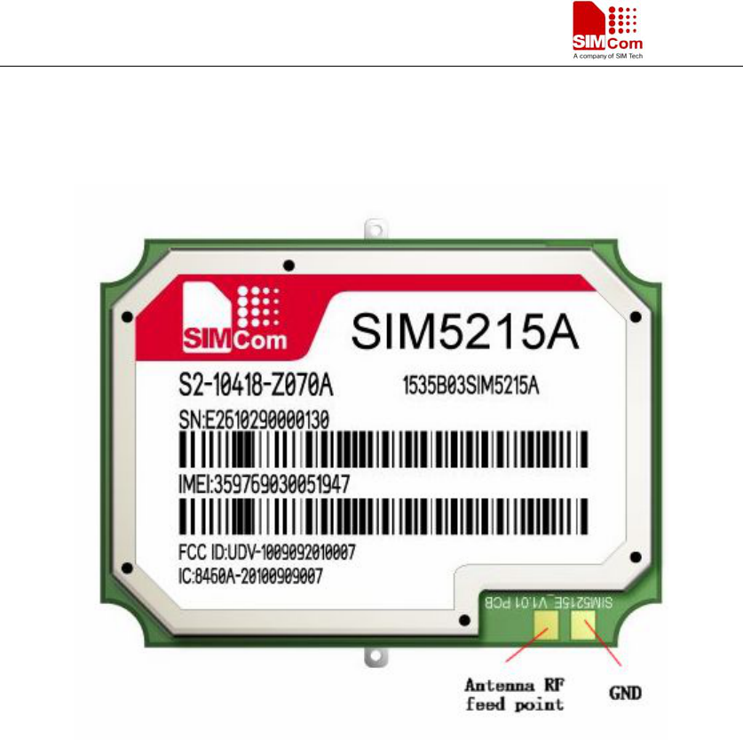
SIM5215A _HD_V1.02 Hardware Design
SIM5215A _HD_V1.02 26.08.2010
58
4.1.2 Antenna pad
The antenna can be soldered to the pad, or attached via contact springs. To help you to ground
the antenna, SIM5215A comes with a grounding plane located close to the antenna pad.
Figure 40: Antenna pad
SIM5215A material properties:
SIM5215A PCB Material: FR4
Antenna pad: Gold plated pad
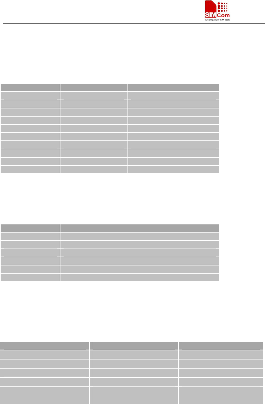
SIM5215A _HD_V1.02 Hardware Design
SIM5215A _HD_V1.02 26.08.2010
59
4.2 Module RF output power
Table 33 : SIM5215A conducted RF output power
Frequency Max Min
GSM850 33dBm ±2db 5dBm±5db
E-GSM900 33dBm ±2db 5dBm±5db
DCS1800 30dBm ±2db 0dBm±5db
P CS1900 30dBm ±2db 0dBm±5db
GSM850(8-PSK) 27dBm ±3db 5dBm±5db
E-GSM900(8-PSK) 27dBm ±3db 5dBm±5db
DCS1800(8-PSK) 26dBm ±3db 0dBm±5db
P CS1900(8-PSK) 26dBm ±3db 0dBm±5db
WCDMA 1900 24dBm+1/-3db <-50dBm
WCDMA 850 24dBm+1/-3db <-50dBm
4.3 Module RF receiver sensitivity
Table 28: SIM5215A conducted RF receive sensitivity
Frequency Receive sensitivity
GSM850 < -107dBm
E-GSM900 < -107dBm
DCS1800 < -107dBm
P CS1900 < -107dBm
WCDMA 1900 < -108dBm
WCDMA 850 < -107dBm
4.4 Module operating frequencies
Table 29: SIM5215A operating frequencies
Frequency Receive Transmit
GSM850 869 ~ 894MHz 824 ~ 849MHz
E-GSM900 925 ~ 960MHz 880 ~ 915MHz
DCS1800 1805 ~ 1880MHz 1710 ~ 1785MHz
P CS1900 1930 ~ 1990MHz 1850 ~ 1910MHz
WCDMA 1900 1930 ~ 1990MHz 1850 ~ 1910MHz
WCDMA 850 869 ~ 894MHz 824 ~ 849 MHz
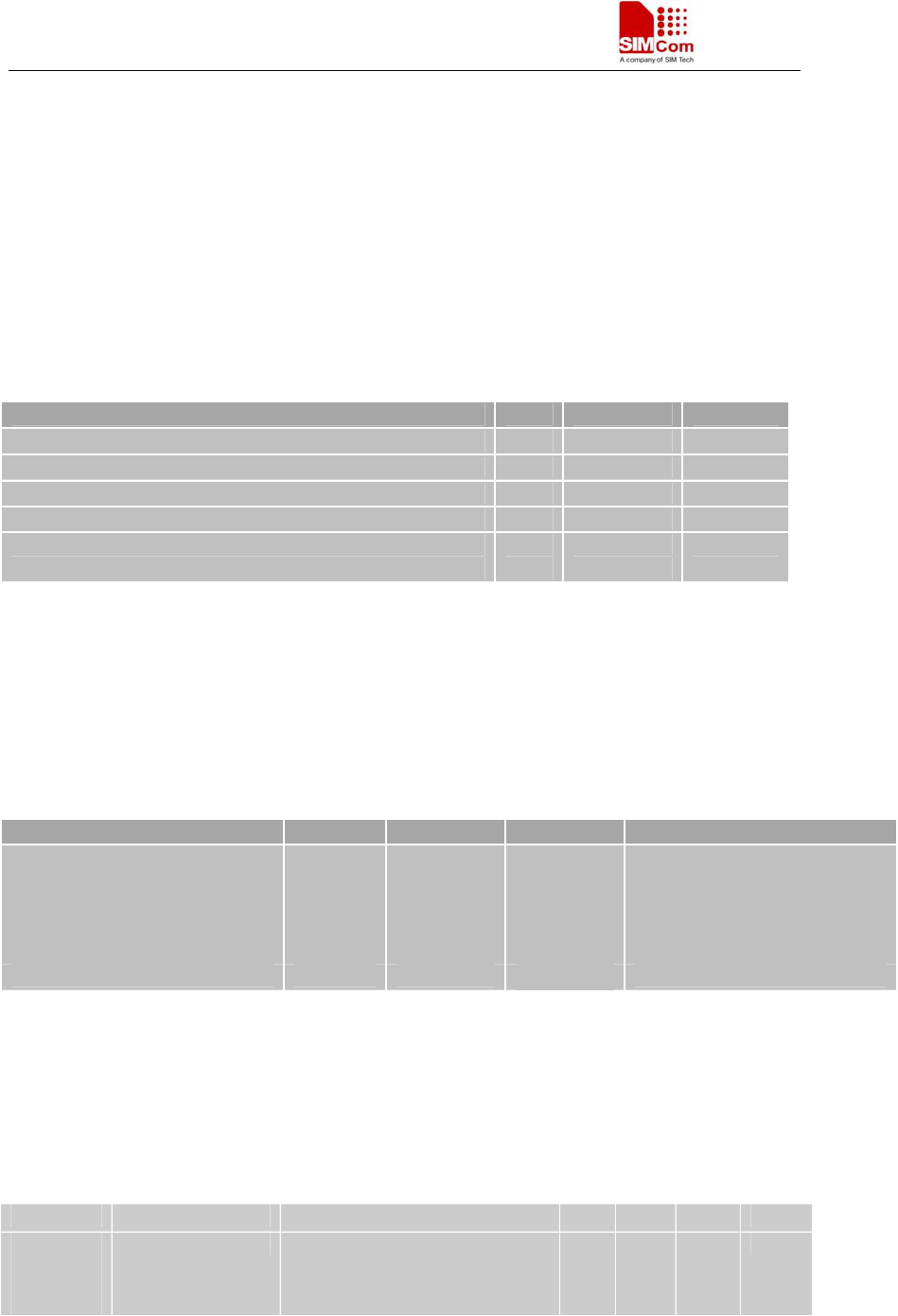
SIM5215A _HD_V1.02 Hardware Design
SIM5215A _HD_V1.02 26.08.2010
60
5 Electrical, reliability and radio characteristics
5.1 Absolute maximum ratings
Absolute maximum rating for power supply and voltage on digital and analog pins of SIM5215A
are list in following table:
Table 30: Absolute maximum ratings
Parameter Min Max Unit
Peak current of power supply 0 3.0 A
RMS current of power supply (during one TDMA- frame) 0 0.9 A
Voltage at digit pins -0.3 3.0 V
Voltage at analog pins -0.3 3.0 V
Voltage at digit/analog pins in POWER DOWN mode -0.25 0.25 V
Voltage at VBAT -0.3 4.4 V
5.2 Operating temperatures
The operating temperature is listed in following table:
Table 31: SIM5215A operating temperature
Parameter Min Max Unit Note
Operating temperature -30 +80 ℃ The module is functional in all
the temperature range, and it
fully meets the
ETSI specifications.
Storage temperature -40 +85 ℃
5.3 Power supply ratings
Table 32: SIM5215A power supply ratings
Parameter Description Conditions Min Typ Max Unit
VBAT
Supply voltage Voltage must stay within the
min/max values, including
voltage drop, ripple, and spikes.
3.3 3.8 4.2 V

SIM5215A _HD_V1.02 Hardware Design
SIM5215A _HD_V1.02 26.08.2010
61
Voltage drop
during transmit
burst
Normal condition, power
control level for Pout max
300 mV
Voltage ripple Normal condition, power
control level for Pout max
@ f<400kHz
@ f>400kHz
50
10
mV
Average supply
current
POWER DOWN mode 35 uA IVBAT
Peak supply
current (during
transmission
slot every 4.7ms)
Power control level for Pout
max.
1.7 2 A
5.4 Current consumption
The values for current consumption in Vbat 3.8V are listed in Table 39. Here, “suspended”
means that SIM5215A is connected with USB BUS but don’t transfer data.
Table 339: SIM5215A current consumption
GSM IDLE mode (without USB suspend)
GSM850 Sleep @DRX=2 3.0mA
Sleep @DRX=5 1.8mA
Sleep @DRX=9 1.4mA
GSM900 Sleep @DRX=2 3.0mA
Sleep @DRX=5 1.86mA
Sleep @DRX=9 1.4mA
DCS1800 Sleep @DRX=2 3.1mA
Sleep @DRX=5 1.7mA
Sleep @DRX=9 1.4mA
PCS1900 Sleep @DRX=2 3.1mA
Sleep @DRX=5 1.6mA
Sleep @DRX=9 1.5mA
GSM IDLE Mode(with USB suspend)
GSM850 Sleep @DRX=2 4.3mA
Sleep @DRX=5 2.8mA
Sleep @DRX=9 2.2mA
GSM900 Sleep @DRX=2 4.3mA
Sleep @DRX=5 2.7mA
Sleep @DRX=9 2.1mA
DCS1800 Sleep @DRX=2 4.4mA
Sleep @DRX=5 2.8mA
Sleep @DRX=9 2.3mA
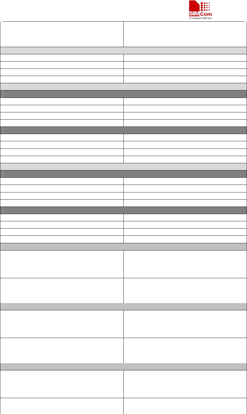
SIM5215A _HD_V1.02 Hardware Design
SIM5215A _HD_V1.02 26.08.2010
62
PCS1900 Sleep @DRX=2 4.4mA
Sleep @DRX=5 2.7mA
Sleep @DRX=9 2.2mA
Voice Call
GSM850 @power level #5 <300mA,Typical 270mA
GSM 900 @power level #5 <310mA,Typical 270mA
DCS1800 @power level #0 <220mA,Typical 210mA
PCS1900 @power level #0 <200mA,Typical 190mA
GPRS Data
DATA mode, GPRS ( 1 Rx,4 Tx ) CLASS 12
GSM 850 @power level #5 <540mA
GSM 900 @power level #5 <500mA
DCS1800 @power level #0 <380mA
PCS1900 @power level #0 <380mA
DATA mode, GPRS ( 3Rx, 2 Tx ) CLASS 12
GSM 850 @power level #5 <390mA
GSM 900 @power level #5 <380mA
DCS1800 @power level #0 <300mA
PCS1900 @power level #0 <250mA
EDGE Data
DATA mode, EDGE( 1 Rx,4 Tx ) CLASS 12
GSM 850 @power level #8 <350mA
GSM 900 @power level #8 <340mA
DCS1800 @power level #2 <325mA
PCS1900 @power level #2 <290mA
DATA mode, EDGE( 3Rx, 2 Tx ) CLASS 12
GSM 850 @power level #8 <250mA
GSM 900 @power level #8 <240mA
DCS1800 @power level #2 <230mA
PCS1900 @power level #2 <210mA
UMTS IDLE Mode (without USB suspend)
WCDMA 1900 Sleep @DRX=9 1.2mA
Sleep @DRX=8 2.1mA
Sleep @DRX=6 4.2mA
WCDMA 850 Sleep @DRX=9 1.2mA
Sleep @DRX=8 2.0mA
Sleep @DRX=6 4.4mA
UMTS IDLE Mode (with USB suspend)
WCDMA 1900 Sleep @DRX=9 1.9mA
Sleep @DRX=8 2.6mA
Sleep @DRX=6 4.6mA
WCDMA 850 Sleep @DRX=9 1.9mA
Sleep @DRX=8 2.7mA
Sleep @DRX=6 4.8mA
UMTS Voice call
WCDMA 1900 @Power 23dBm Typical 580mA
@Power 10dBm Typical 205mA
@Power-55dBm Typical 174mA
WCDMA 850 @Power 23dBm Typical 510mA
@Power 10dBm Typical 195mA
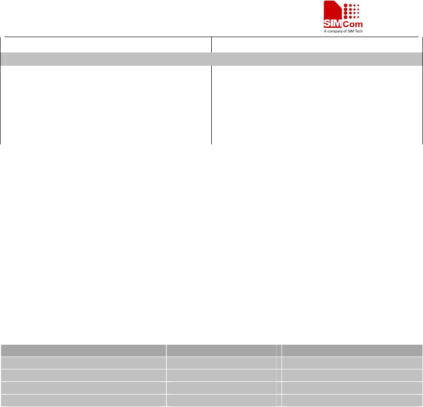
SIM5215A _HD_V1.02 Hardware Design
SIM5215A _HD_V1.02 26.08.2010
63
@Power-55dBm Typical 131mA
HSDPA Data(only 5216A)
WCDMA 1900
@Power 23dBm Typical 584mA
@Power 10dBm Typical 331mA
@Power-55dBm Typical 179mA
WCDMA 850
@Power 23dBm Typical 536mA
@Power 10dBm Typical 231mA
@Power-55dBm Typical 165mA
5.5 Electro-Static discharge
Normally SIM5215A is mounted on customer host board, although some ESD components have
been added in SIM5215A, to improve ESD, one should put some ESD components on customer
host board. The ESD components should be placed beside the connectors which the human body
might touch, such as SIM card holder, T-flash card holder, audio jacks, switches, keys, etc..
Below is the SIM5215A ESD performance measurement table, the results are got from our EVB
board test.
Table 40: The ESD performance measurement table (Temperature: 25 , Humidity:℃ 45% )
Part Contact discharge Air discharge
VBAT,GND ±4KV ±10KV
UART,USB ±4KV ±8KV
Antenna port ±4KV ±10KV
Other port ±3KV ±8KV
In order to get the best ESD performance, one must deal carefully with ground of SIM5215A
on host board, which is most important. Here are some advices:
1. Bare the copper on the host board.
Figure 36 is SIM5215A PCB decal. There is a big area which is poured with copper.
When one mounts the SIM5215A on host board, the bottom shield of SIM5215A can be
connected to ground well through this copper area. The SIM5215A PCB decal can be got
from our FAE or sales people.
2. Choose 2.0mm height 70-pin socket for host board.
Because the height of 70-pin plug on SIM5215A is 1.5mm, in order to better connecting the
SIM5215A to the ground of the host board, it is suggested to choose 2.0mm height 70-pin socket
for host board. NAS AXK770247G is suitable. 2.5mm will be too high, it will be suspending
above host board. 1.5mm will be too tight.
3. Fill some conductors between the bottom of SIM5215A and host board.
Figure 37 shows the conductor material we use. Other conductor material can be used as well.
4. Solder SIM5215A to ground through 2 out-feet of bottom shield.
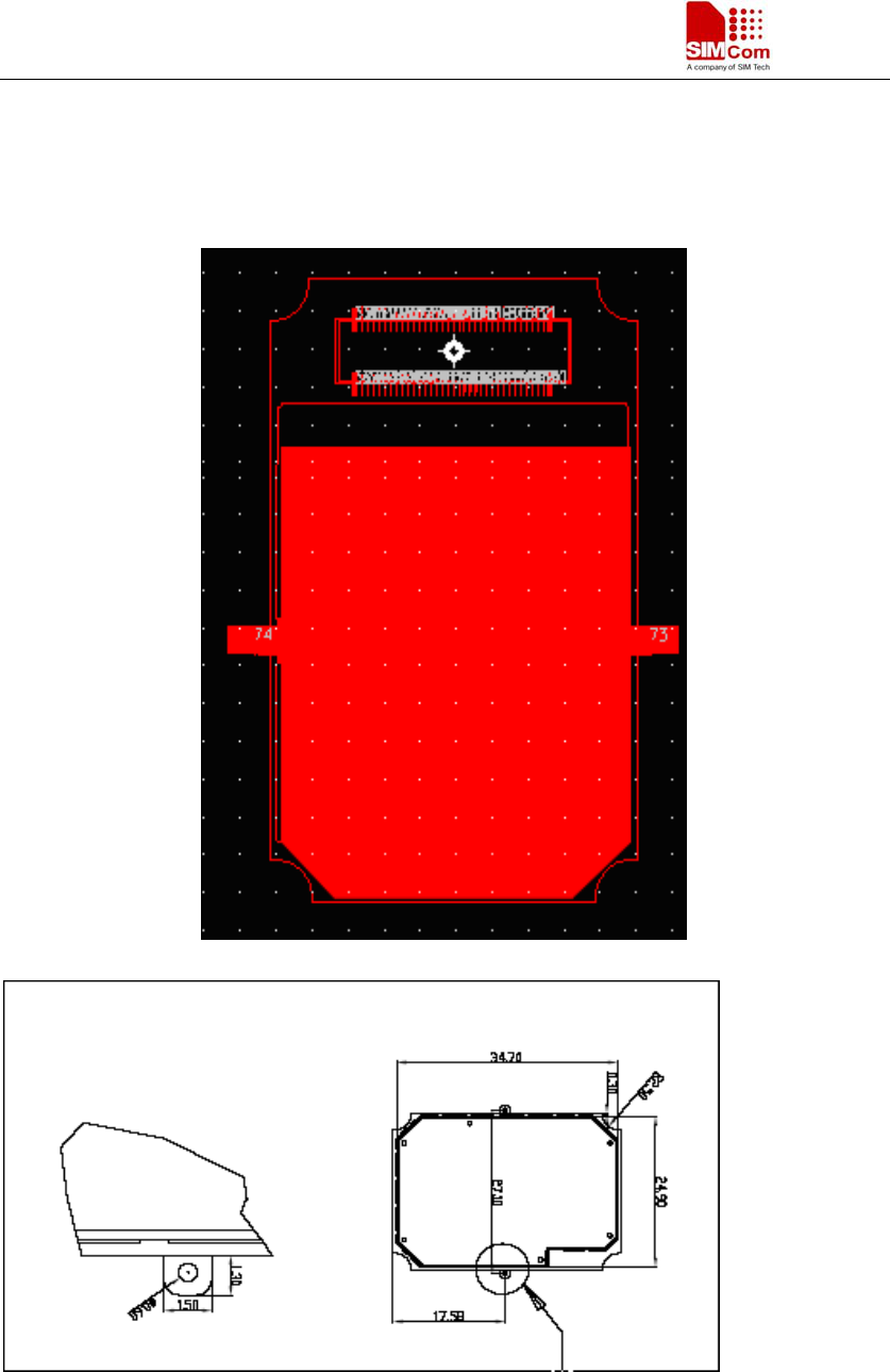
SIM5215A _HD_V1.02 Hardware Design
SIM5215A _HD_V1.02 26.08.2010
64
There are 2 out-feet of SIM5215A bottom shield. One can solder them to bare cooper on host
board, so that SIM5215A can be connected to the ground well.
Figure 41: SIM5215A PCB decal
Figure 42: SIM5215A Soldering 2 out-feet of bottom shieding to host board
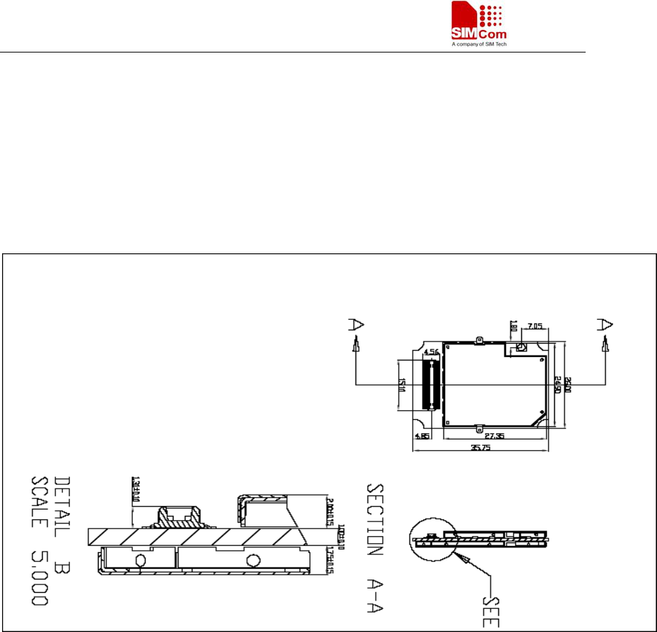
SIM5215A _HD_V1.02 Hardware Design
SIM5215A _HD_V1.02 26.08.2010
65
6 Mechanics
This chapter describes the mechanical dimensions of SIM5215A.
6.1 Mechanical dimensions of SIM5215A
Following are SIM5215A top view, side view and bottom view. These show you Mechanical
dimensions of SIM5215A.
Figure 43: Mechanical dimensions of SIM5215A(Unit: mm)
6.2 Mounting SIM5215A onto the application platform
Use the connector AXK870145WG and four mounting pads to fix the SIM5215A onto the
customer platform.
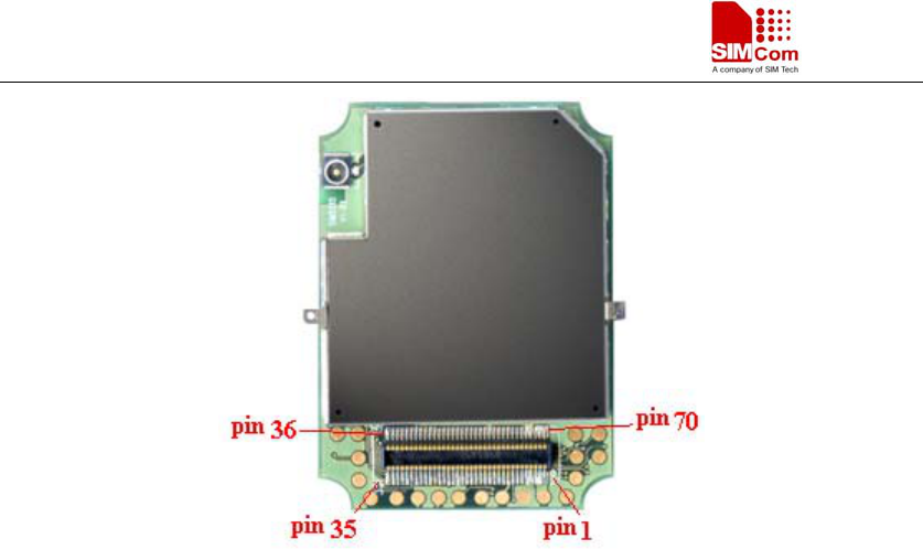
SIM5215A _HD_V1.02 Hardware Design
SIM5215A _HD_V1.02 26.08.2010
66
Figure 44: PIN sequence of SIM5215A
When one mounts SIM5215A on host board, please pay attention to that the pin sequence of
SIM5215A is mirror image of pin sequence of 70-pin socket connector on host.
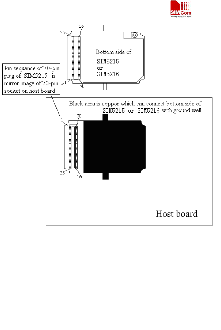
SIM5215A _HD_V1.02 Hardware Design
SIM5215A _HD_V1.02 26.08.2010
67
Figure 45: Mirror image of pin sequence
6.3 Board-to-board connector
We recommend users to adopt NAIS AXK770247G as the board to board connector in their own
PCB to connect with SIM5215A. These high density SMT connectors are designed for parallel
PCB-to-PCB applications. They are ideal for using in VCRs, notebook PCs, cordless telephones,
mobile phones, audio/visual and other telecommunications equipment where reduced size and
weight are important. The height of AXK770247G is 2.0mm.
Following are parameters of AXK770247G for more details, you can login
http://www.NAIS-E.com for more information.
Mechanical dimensions of the NAIS 70pin connector
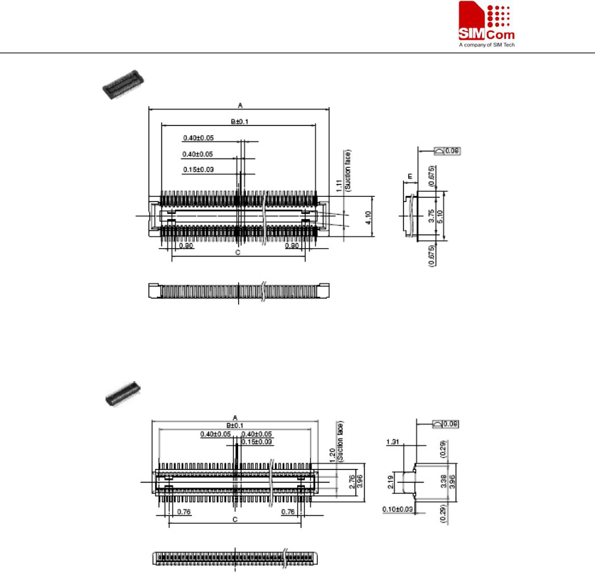
SIM5215A _HD_V1.02 Hardware Design
SIM5215A _HD_V1.02 26.08.2010
68
Figure 46: NAIS AXK770247G board-to-board connector pin side
Figure 47: NAIS AXK870145WG board-to-board connector pin side
NOTE
:
The connector NAIS AXK870145WG is used in SIM5215A side and NAIS
AXK770247G is used in pin side (host board side).
6.4 RF connector and adapter cable
The RF connector in module side is Murata Company RF Connectors MM9329-2700, it makes a
pair with Murata Company RF cable MXTK88TK2000. It has high performance with wide
frequency range, surface mountable and reflow solderable. Following are parameters.
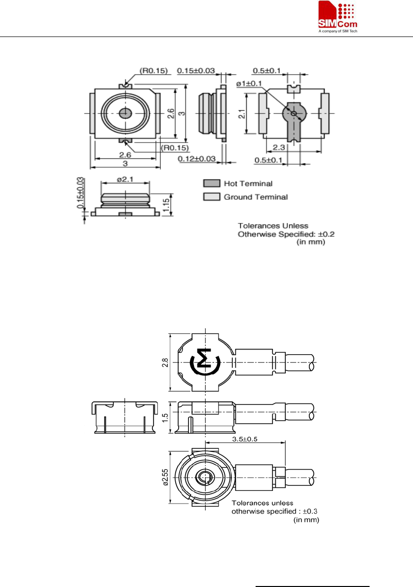
SIM5215A _HD_V1.02 Hardware Design
SIM5215A _HD_V1.02 26.08.2010
69
Figure 48: RF connector MM9329-2700
Figure 49: RF adapter cable MXTK88TK2000
For more information about the connector, please visit http://www.murata.com/
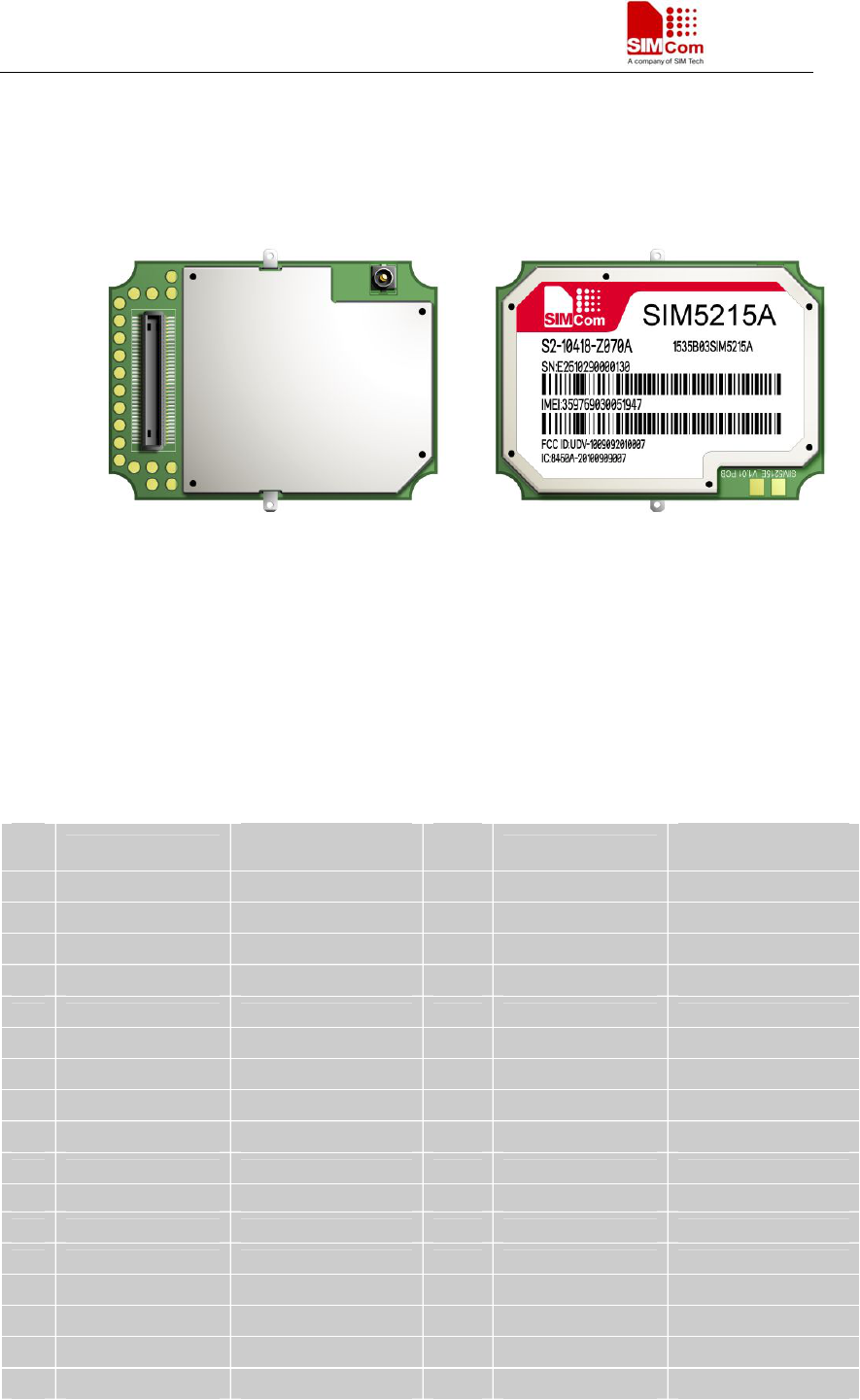
SIM5215A _HD_V1.02 Hardware Design
SIM5215A _HD_V1.02 26.08.2010
70
6.5 View of the SIM5215A
Bottom View Top View
Figure 50: Top and Bottom View of SIM5215A
6.6 PIN assignment of board-to-board connector of SIM5215A
Table 34 : Connection diagrams
Pin
No Define Measure without
usage Pin
No Define Measure without
usage
1 VBAT VBAT 70 VBAT VBAT
2 VBAT VBAT 69 VBAT VBAT
3 VBAT VBAT 68 VBAT VBAT
4 GND GND 67 GND GND
5 GND GND 66 GND GND
6 UART_TXD NC 65 GPIO0 NC
7 UART_CTS NC 64 UART_RXD NC(See Note)
8 UART_DCD NC 63 UART_RTS NC
9 USB_VBUS NC 62 UART_DTR NC
10 GPIO1 NC 61 UART_RI NC
11 VRTC NC 60 USB_D_P NC
12 USIM_CLK NC 59 USB_D_M NC
13 USIM_RESET NC 58 GND GND
14 Reserved NC 57 V_USIM NC
15 CAM_D2 NC 56 USIM_DATA NC(See Note)
16 CAM_D4 NC 55 Reserved NC
17 CAM_D6 NC 54 CAM_D3 NC

SIM5215A _HD_V1.02 Hardware Design
SIM5215A _HD_V1.02 26.08.2010
71
18 CAM_D8 NC 53 CAM_D5 NC
19 CAM_HSYNC NC 52 CAM_D7 NC
20 GND GND 51 CAM_D9 NC
21 CAM_CLK NC 50 CAM_VSYNC NC
22 CAM_STANDBY NC 49 CAM_PCLK NC
23 SPK_P NC 48 CAM_RESET NC
24 SPK_N NC 47 IIC_SDA NC(See Note)
25 EAR_P NC 46 IIC_SCL NC(See Note)
26 EAR_N NC 45 POWER_ON NC
27 HPR NC 44 MIC_N 0.1u cap to ground
28 HPL NC 43 MIC_P 0.1u cap to ground
29 RESET NC 42 HP_MICP NC
30 GPIO2 NC 41 HKADC NC
31 GPIO3 NC 40 VREG_AUX NC
32 GPIO4 NC 39 SD_DATA3 NC
33 GPIO5 NC 38 SD_DATA2 NC
34 SD_CLK NC 37 SD_DATA1 NC
35 SD_CMD NC 36 SD_DATA0 NC
Note: UART_RXD has been pulled down with a 15kR resistor to ground in module.
USIM DATA has been pulled up with a 22kR resistor to V_USIM in module.
IIC_SDA and IIC_SCL have been pulled up with two 2.2kR resistors to 2.6V in module. So
there is no need to pull them up or down in your application circuit.
Contact us:
Shanghai SIMCOM Wireless Solutions Ltd.
Add: SIM Technology Building,No.633,Jinzhong Road,Changning District,
Shanghai P.R. China 200335
Tel: +86 21 3235 3300
Fax: +86 21 3235 3301
URL: www.sim.com/wm