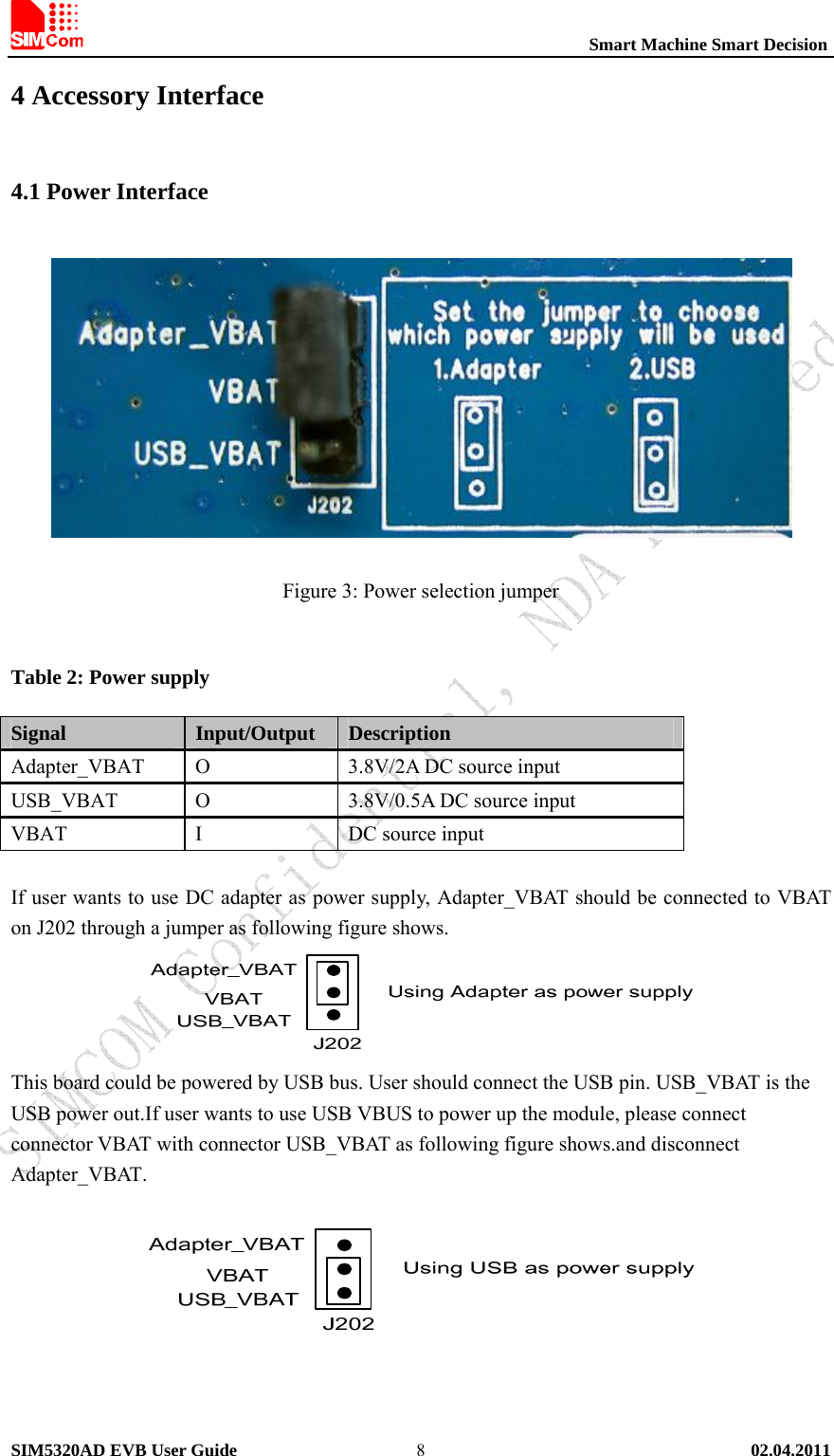
Simcom 1103022011009 Wireless Module User Manual SIM5320AD 20111216
Shanghai Simcom Ltd. Wireless Module SIM5320AD 20111216
UserManual.wiki
>
Simcom
>
1103022011009 User Manual
(SIM5320AD)User Manual_20111216
Navigation menu
Upload a User Manual
Namespaces
Wiki Guide
HTML
PDF
Info
Views
User Manual
Discussion / Help
Navigation
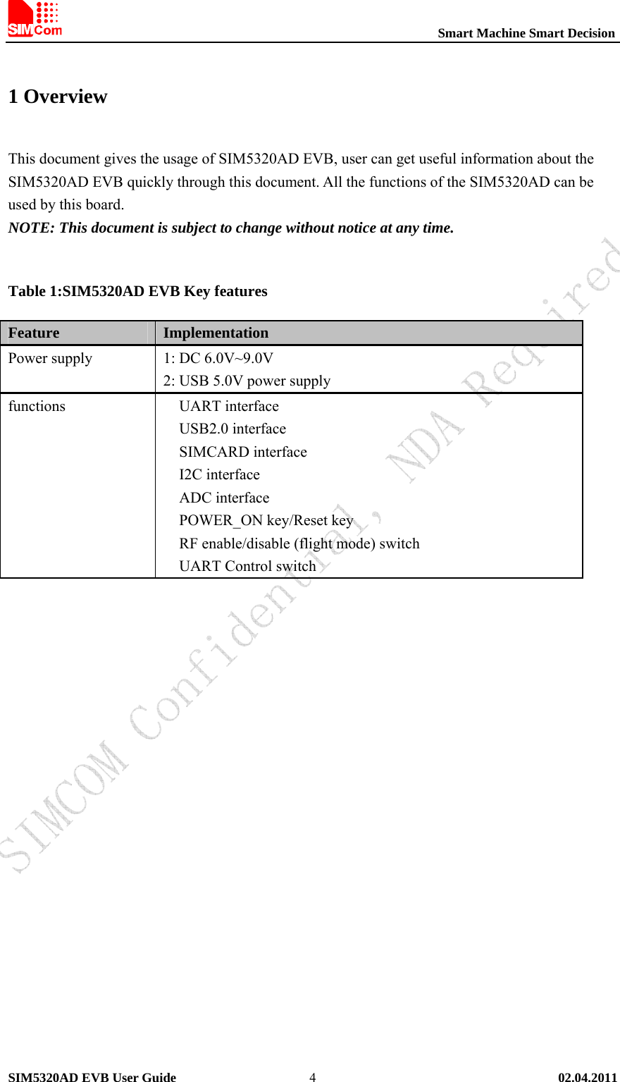
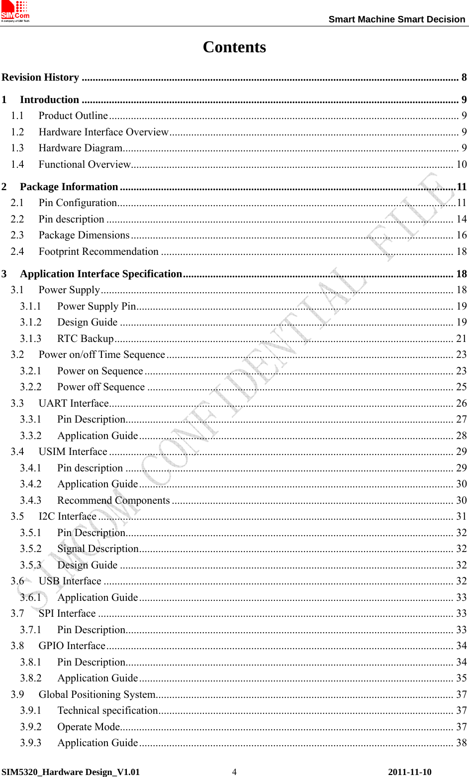
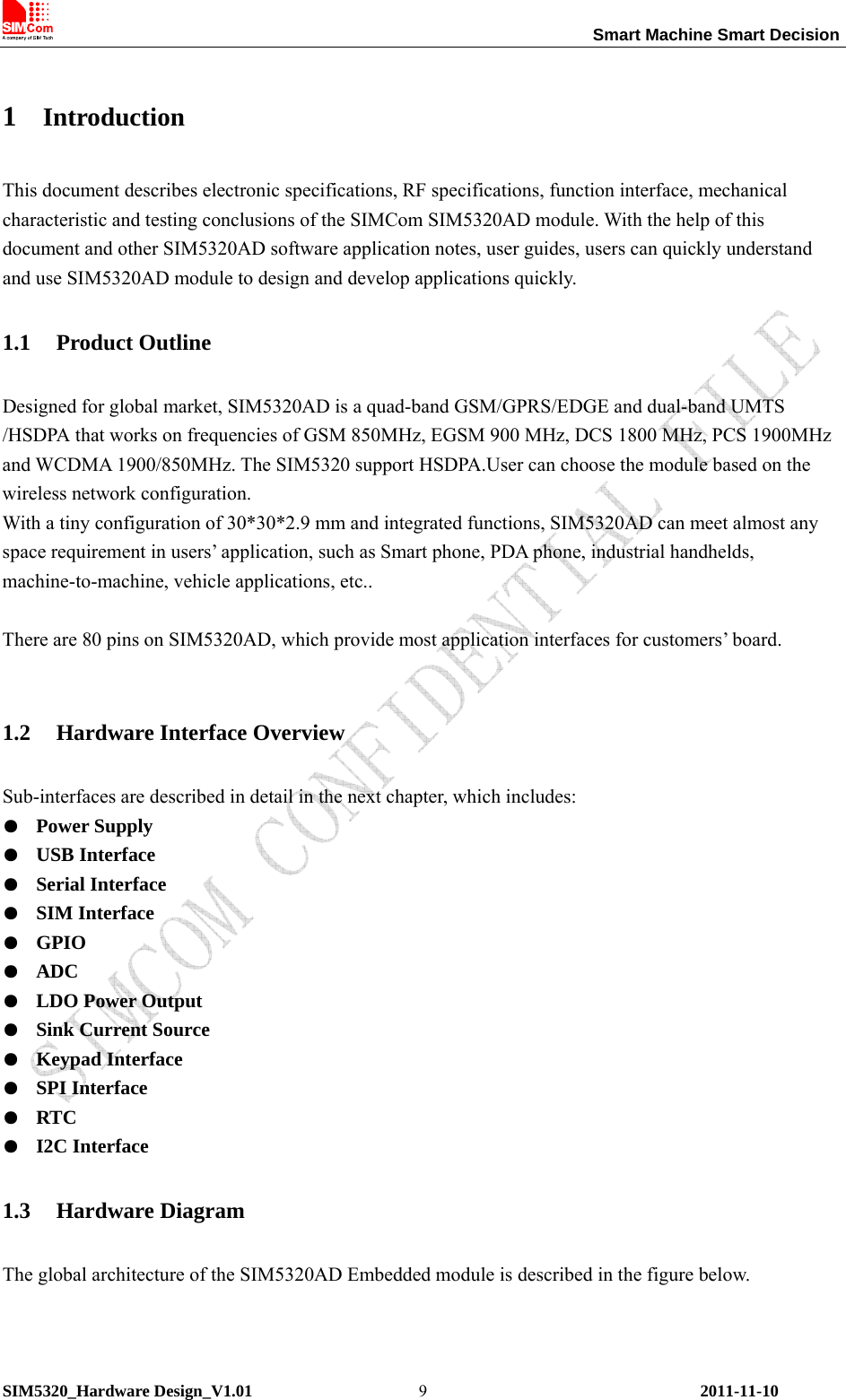
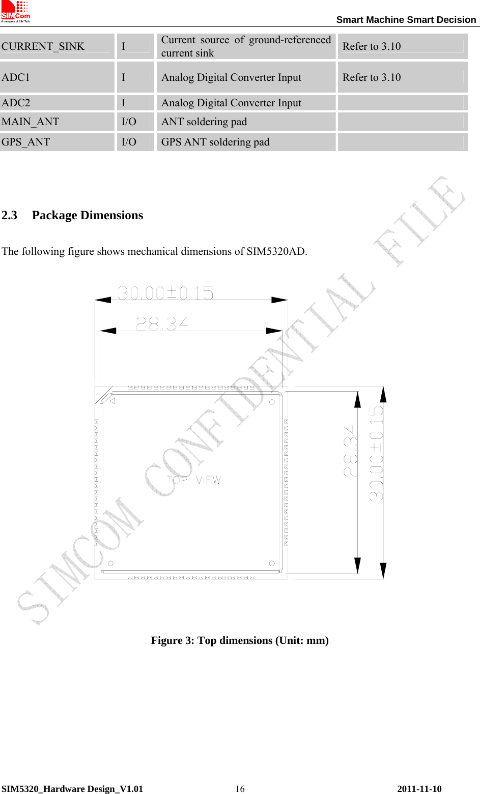
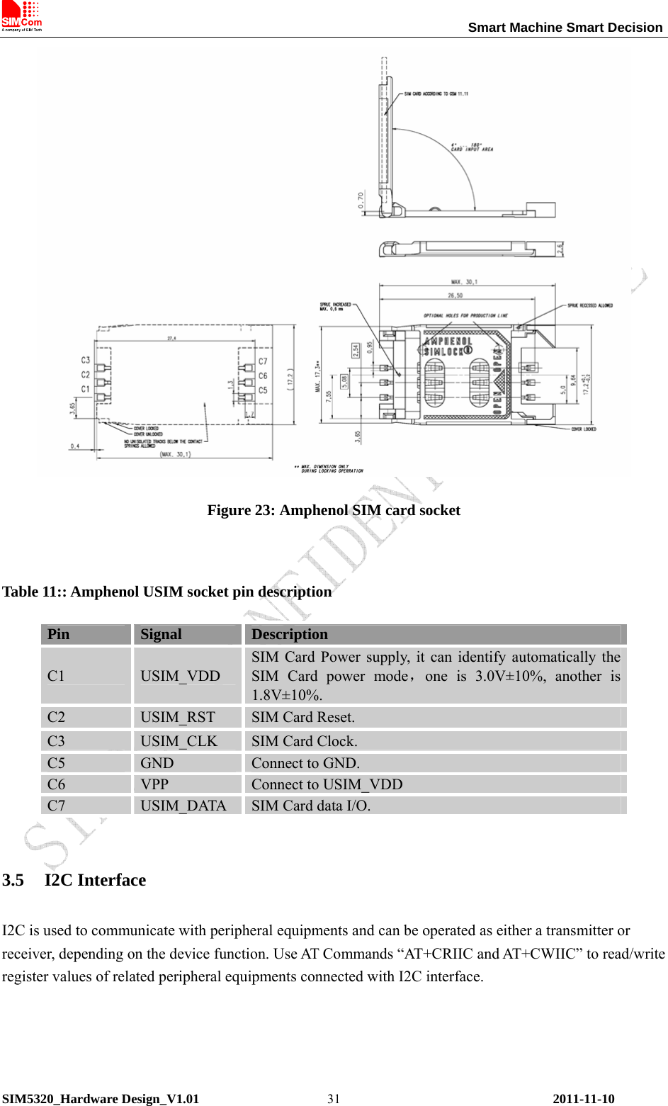
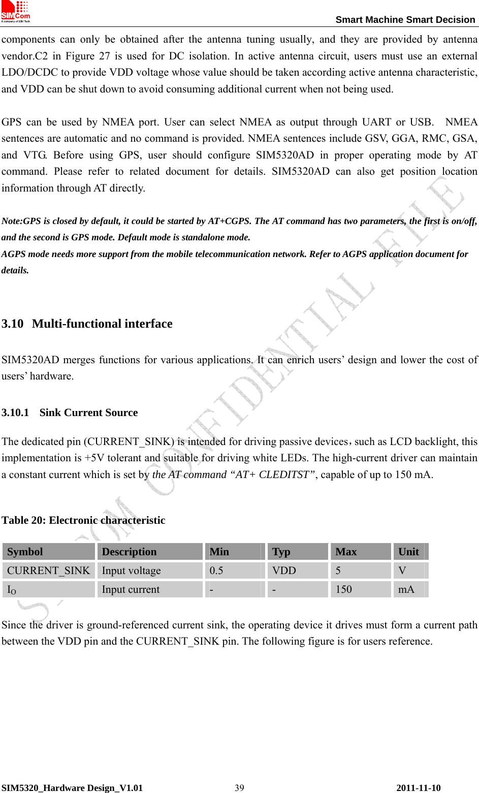
![Smart Machine Smart Decision SIM5320_Hardware Design_V1.01 2011-11-10 21 Figure 10: Reference circuit of the DCDC power supply Voltage monitor To monitor the power supply voltage, user can use the AT command “AT+CBC”, this command has two parameters: the battery status and the voltage value (mV). It will return the capacity percentage and actual value of battery (at the VBAT_BB pin). The voltage is continuously measured at intervals, whenever the measured battery voltage is lower than a specific value set by the AT command “AT+CVALARM”. For example, if the voltage value is set to be 3.4V, the following URC will be presented: “warning! voltage is low: 3.3v”. If the voltage is lower than a specific value which is set by the AT command “AT+CPMVT”, the module will be powered off automatically and AT commands cannot be executed any more. Note: Under-voltage warning function is disabled by default, user can enable it by the AT command “AT+CVALARM”. Auto power off feature is disabled by default, user should set it by the AT command “AT+CPMVT” to an appropriate value. Please refer to Document [1]. 3.1.3 RTC Backup The module uses RTC (Real Time Clock) to update and maintain inherent time and keeps system alive at no power supply status. The RTC power supply of module can be provided by an external capacitor or a battery (non-chargeable or rechargeable) through the VRTC. The following figures show various reference circuits for RTC back up. The discharge current is less than 10uA. If this feature is used, please refer to the AT commands “AT+CTZU” and “AT +CTZR”. z External capacitor backup](https://usermanual.wiki/Simcom/1103022011009/User-Guide-1603965-Page-42.png)
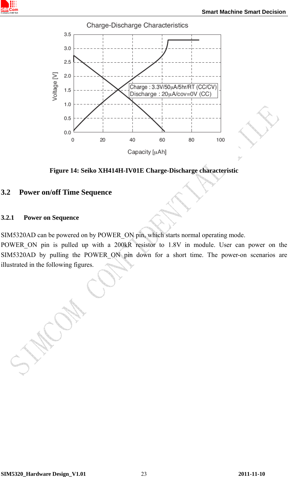
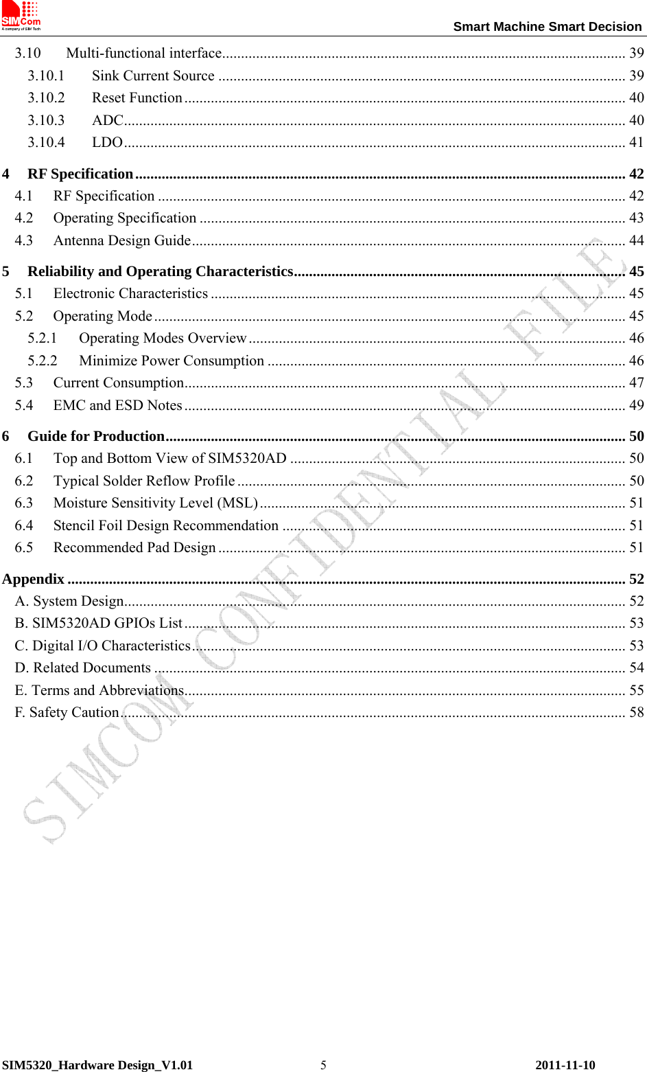
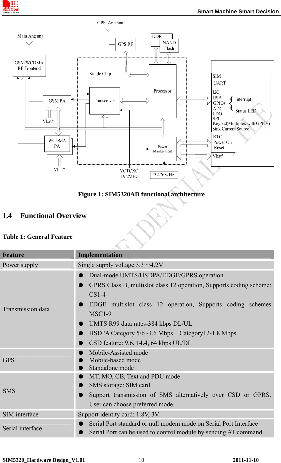
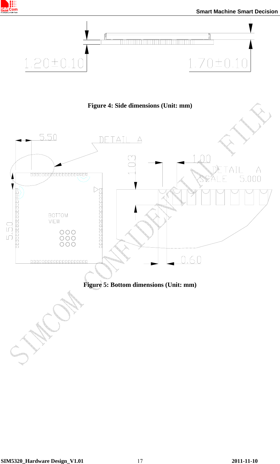
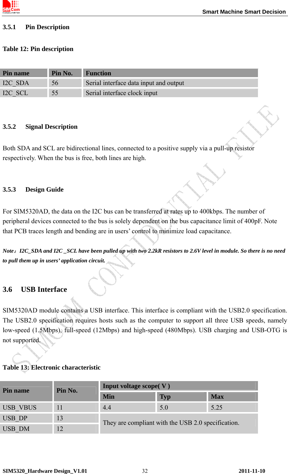
![Smart Machine Smart Decision SIM5320_Hardware Design_V1.01 2011-11-10 26 Figure 17: Power off timing sequence Table 6: Power off timing Parameter Description Time value Unit Toff The time pulling POWER_ON down to power off 0.5< Toff<5 s TpD- The time to indicate disconnecting from the network >7 s Tpw- The time to indicate the module power off completely >7.5 s Tuart_off The time to disable UART >6 s Tusb_off The time to disable USB >7.5 s User can also use the AT command “AT + CP O F” to power down the module. After that, the AT commands cannot be executed any longer. The module enters the POWER DOWN mode, only the RTC is still active. For details, refer to Document [1]. 3.3 UART Interface SIM5320AD provides a UART (universal asynchronous serial transmission) port. It consists of a flexible 7-wire serial interface. The module is as the DCE (Data Communication Equipment) and the client PC is as the DTE (Data Terminal Equipment). AT commands are entered and serial communication is performed through UART interface. The application circuit is in the following figures.](https://usermanual.wiki/Simcom/1103022011009/User-Guide-1603965-Page-47.png)
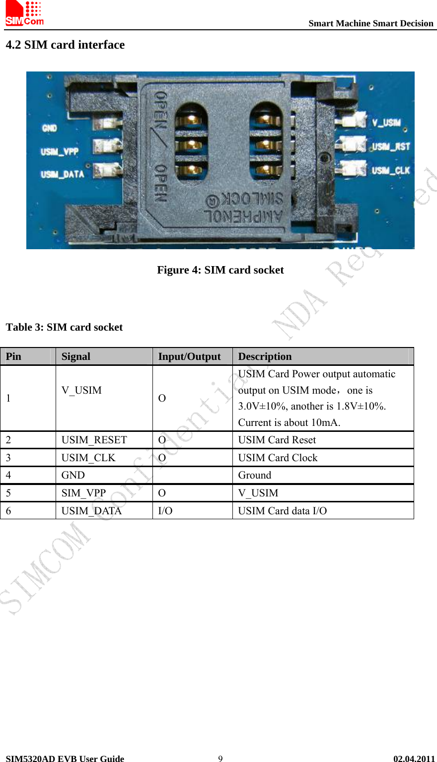
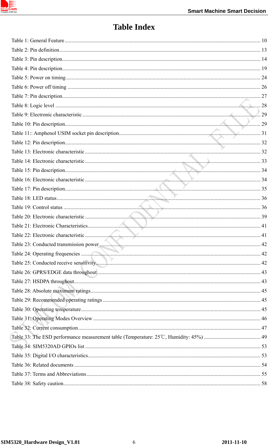
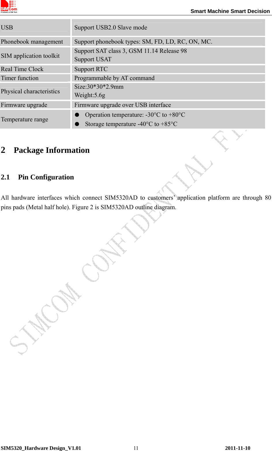
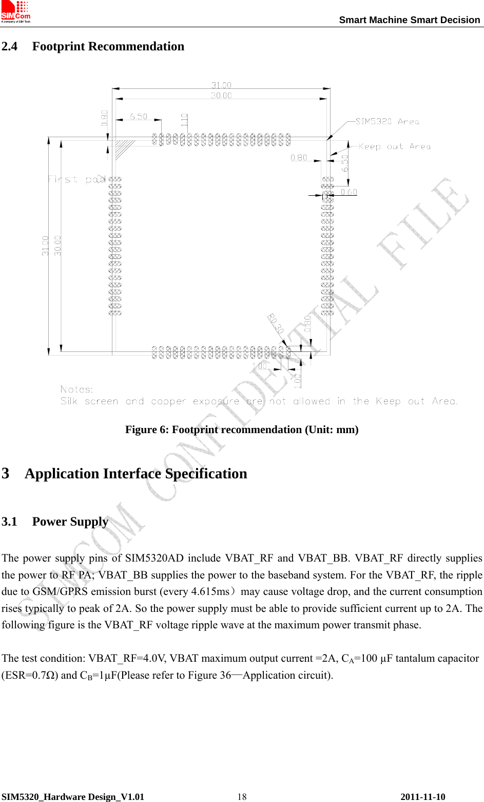
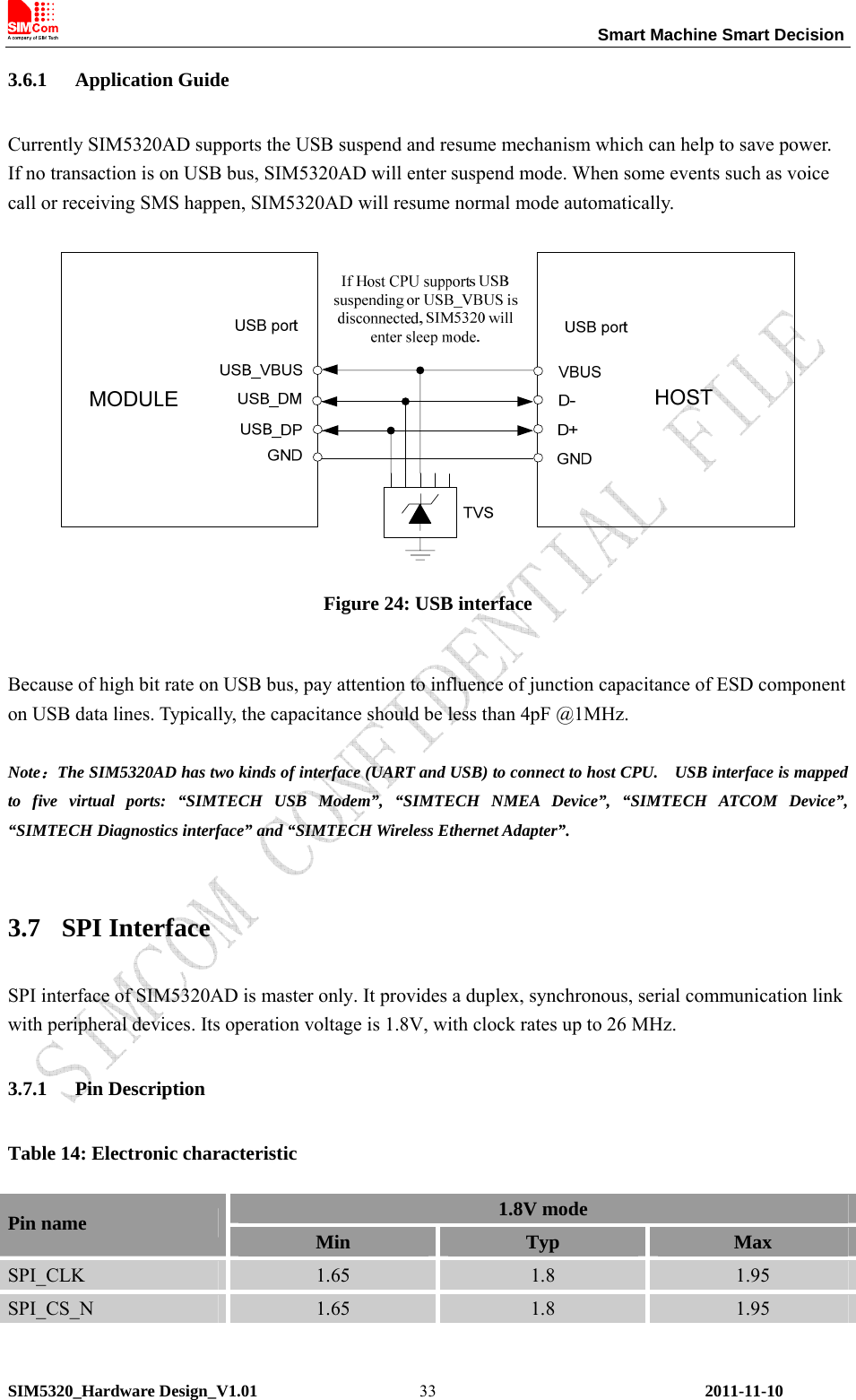
![Smart Machine Smart Decision SIM5320_Hardware Design_V1.01 2011-11-10 303.4.2 Application Guide It is recommended to use an ESD protection component such as ST (www.st.com ) ESDA6V1W5 or ON SEMI (www.onsemi.com ) SMF05C. Note that the SIM peripheral circuit should be close to the SIM card socket. The reference circuit of the 8-pin SIM card holder is illustrated in the following figure. Figure 22: USIM interface reference circuit Note: USIM_DATA has been pulled up with a 22kR resistor to V_USIM in module. A 220nF shut capacitor on V_USIM is used to reduce interference. Use AT Commands to get information in USIM card. For more detail, please refer to document [1]. 3.4.3 Recommend Components For 6 pins USIM socket, SIMCom recommend to use Amphenol C707 10M006 512 2. User can visit http://www.amphenol.com for more information about the holder.](https://usermanual.wiki/Simcom/1103022011009/User-Guide-1603965-Page-51.png)
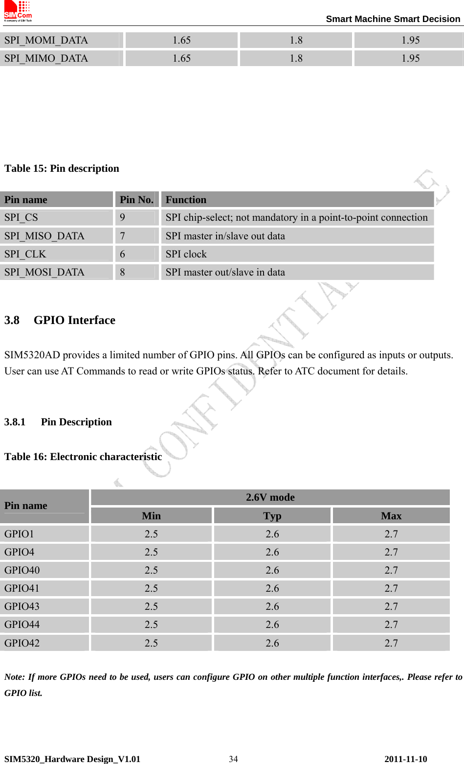
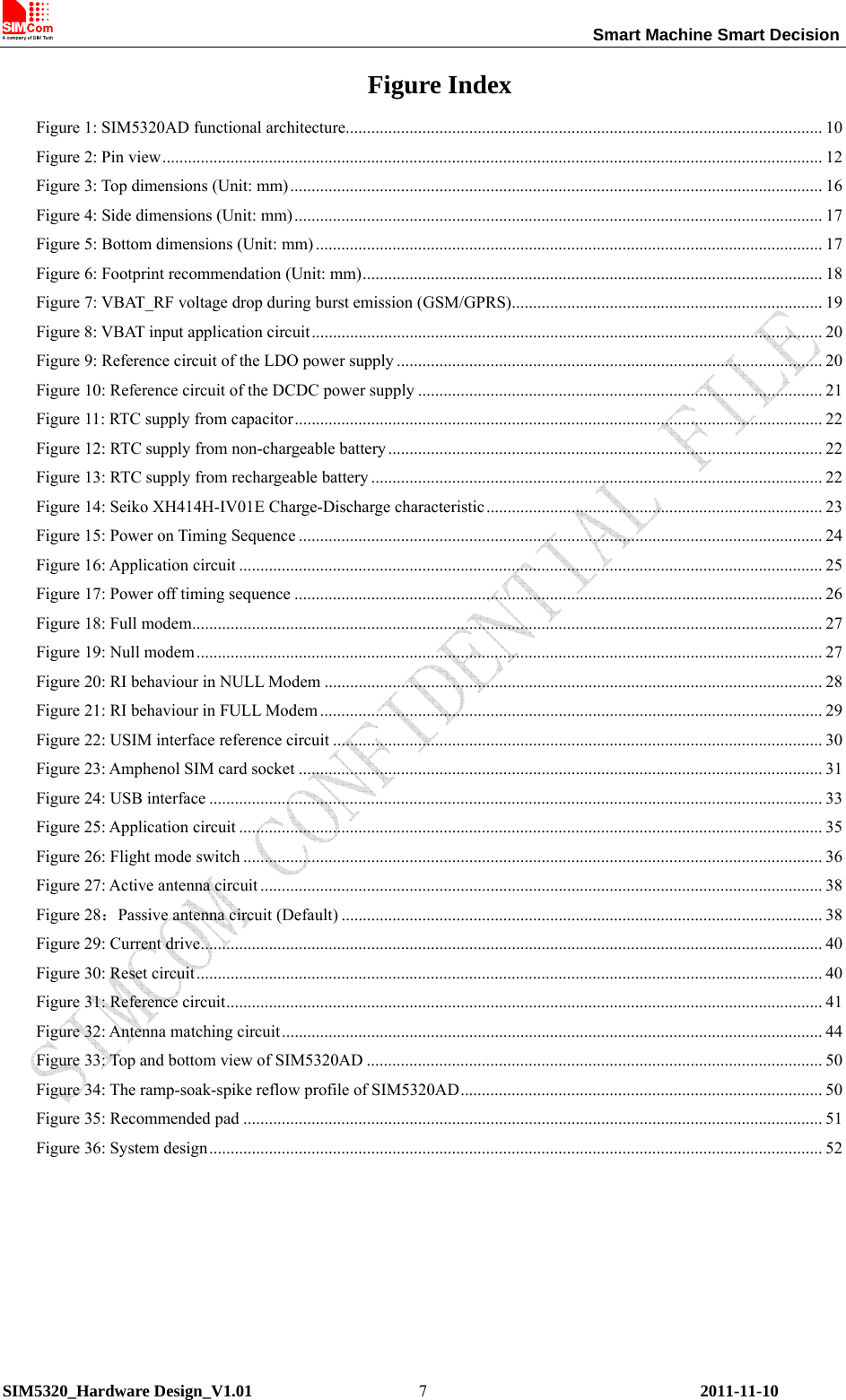
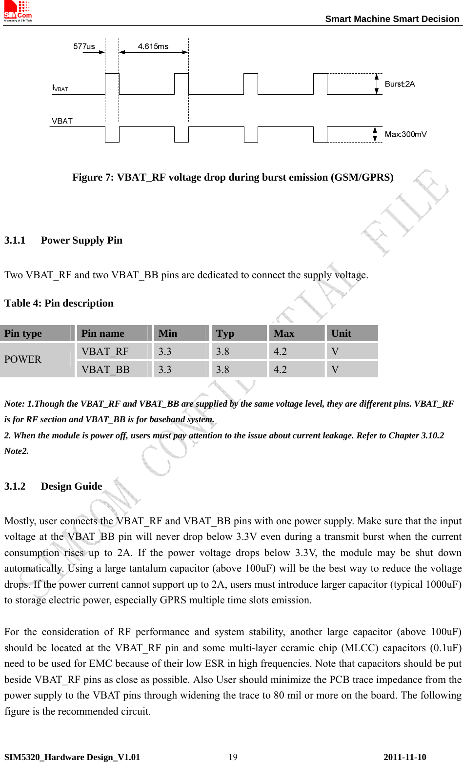
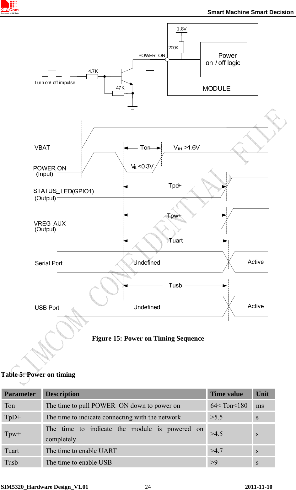
![Smart Machine Smart Decision SIM5320_Hardware Design_V1.01 2011-11-10 41and so on; it is on PIN 47 and PIN 46 , namely ADC1 and ADC2 . This ADC is 12 bit successive-approximation circuit, and electronic specification is shown in the following table. Table 21: Electronic Characteristics Specification Min Typ Max Unit Comments/Conditions Resolution 12 Bits Differential nonlinearity -4 +4 LSB Integral nonlinearity -8 +8 LSB Gain Error -2.5 +2.5 % Offset Error -4 +40 LSB Analog Vdd = ADC reference 2.4MHz sample rate Input Range GND 2.2V V Input serial resistance 2 kΩ Sample and hold switch resistance Input capacitance 53 pF Power-down to wakeup 9.6 19.2 μs User can introduce a signal in the ADC pin directly and use the AT command “AT+CADC” to get the raw data which is between 0 and 255. The data can be transformed to any type such as voltage, temperature etc. Please refer to Chapter 3.1.2 and document [1]. Figure 31: Reference circuit Note: The input signal voltage value in ADC must not be higher than 2.2V. 3.10.4 LDO SIM5320AD has a LDO power output, namely VREG_AUX. The LDO is available and output voltage is 2.85v by default, rated for 250mA. User can switch the LDO on or off by the AT command “AT+CVAUXS” and configure its output voltage by the AT command “AT+CVAUXV”. Table 22: Electronic characteristic Symbol Description Min Typ Max Unit VREG_AUX Output voltage 1.5 2.85 3.05 V IO Output current - - 250 mA](https://usermanual.wiki/Simcom/1103022011009/User-Guide-1603965-Page-62.png)
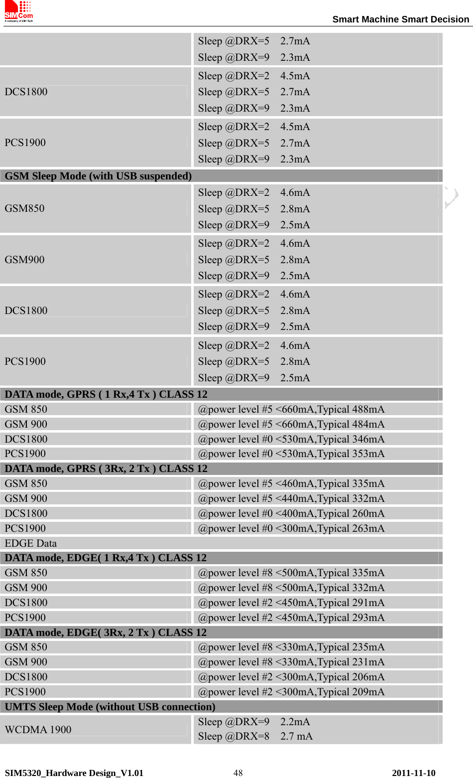
![Smart Machine Smart Decision SIM5320_Hardware Design_V1.01 2011-11-10 47Sleep mode If peripheral equipments stops working, and there is no on air or hardware interrupts (such as GPIO interrupts or data on UART), SIM5320AD will enter sleep mode automatically. In this mode, SIM5320AD can still receive paging,voice call or SMS from network. If USB interface of SIM5320AD is connected to host CPU, but host CPU does not support USB suspending, then SIM5320AD will not enter sleep mode. After USB is disconnected, SIM5320AD will enter sleep mode. Note: When UART interface is connected with host CPU, SIM5320AD can not enter sleep mode until RXD is pulled down by the host CPU. If the module is in the idle mode, make sure to pull the RXD to low level by host CPU. SIMCom recommends using GPIO43 or UART_DTR to wake up the module from host CPU and to use GPIO41 or UART_RI to wake up the host CPU. Before designing, pay attention to how to realize waking function and refer to Document[24] and Document[25] for more detail. Minimum functionality mode Minimum functionality mode ceases a majority function of module, thus minimizing the power consumption. This mode is set by the AT command which provides a choice of the functionality levels. ● AT+CFUN=0: Minimum functionality ● AT+CFUN=1: Full functionality (Default) ● AT+CFUN=4: Disable RF function of the module (Flight mode) If SIM5320AD has been set to minimum functionality mode, the module will firstly enter sleep mode, then the RF function and SIM card function will be closed. In this case, the serial port is still accessible, but RF function or SIM card will be unavailable. When SIM5320AD is in minimum functionality or flight mode, it can return to full functionality by the AT command “AT+CFUN=1”. Note: For flight mode, please refer to Chapter3.9.2. 5.3 Current Consumption The current consumption in suspended mode and without USB connection is listed in the table below. Here, “suspended mode” means that SIM5320AD is connected to USB bus, but it does not transfer data. Table 32: Current consumption GSM Sleep mode (without USB connection) GSM850 Sleep @DRX=2 4.5mA Sleep @DRX=5 2.7mA Sleep @DRX=9 2.3mA GSM900 Sleep @DRX=2 4.5mA](https://usermanual.wiki/Simcom/1103022011009/User-Guide-1603965-Page-68.png)
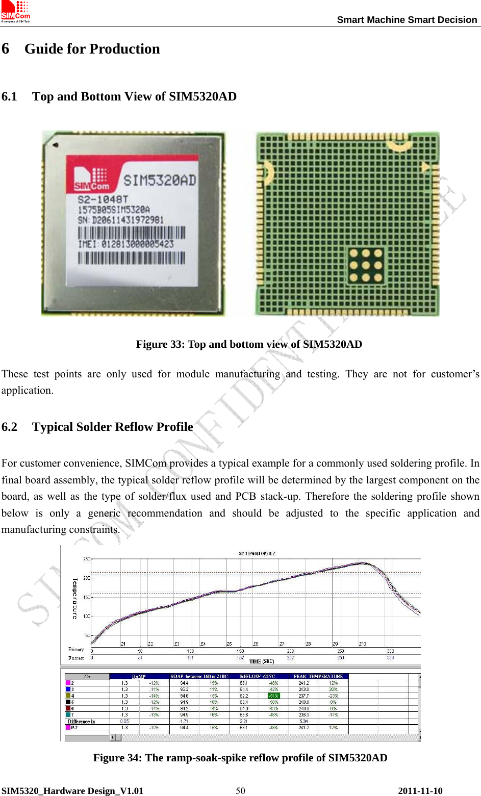
![Smart Machine Smart Decision SIM5320_Hardware Design_V1.01 2011-11-10 51For details about secondary SMT, please refer to document [23]. 6.3 Moisture Sensitivity Level (MSL) SIM5320AD is qualified to Moisture Sensitivity Level (MSL) 5 in accordance with JEDEC J-STD-020. After the prescribed time limit exceeded, users should bake modules for 192 hours in drying equipment (<5% RH) at 40° C +5° C/-0° C, or 72 hours at 85° C +5° C/-5° C. Note that plastic tray is not heat-resistant, users must not use the tray to bake at 85° C or the tray may be damaged. 6.4 Stencil Foil Design Recommendation The recommended thickness of stencil foil is more than 0.15mm. 6.5 Recommended Pad Design Module OutlineABA:B=1.0mm:0.8mm Figure 35: Recommended pad Note: More designing details refer to Figure 6.](https://usermanual.wiki/Simcom/1103022011009/User-Guide-1603965-Page-72.png)
![Smart Machine Smart Decision SIM5320_Hardware Design_V1.01 2011-11-10 54IIH Input high leakage current - - 1 - - 1 uA IIL Input low leakage current -1 - - -1 - - uA CIN Input capacitance - - 7 - - 7 pF Note: These parameters are for digital interface pins, such as keypad, GPIO, I2C, UART, SPI and DEBUG. The SIM5320AD includes two kinds of voltages: 1.8v and 2.6v. Digital I/O specifications under both conditions are presented in the above tables. D. Related Documents Table 36: Related documents SN Document name Remark [1] SIM5320AD_ATC_V1.00 SIM5320AD_ATC_V1.00 [2] ITU-T Draft new recommendationV.25ter Serial asynchronous automatic dialing and control [3] GSM 07.07 Digital cellular telecommunications (Phase 2+); AT command set for GSM Mobile Equipment (ME) [4] GSM 07.10 Support GSM 07.10 multiplexing protocol [5] GSM 07.05 Digital cellular telecommunications (Phase 2+); Use of Data Terminal Equipment – Data Circuit terminating Equipment (DTE – DCE) interface for Short Message Service (SMS) and Cell Broadcast Service (CBS) [6] GSM 11.14 Digital cellular telecommunications system (Phase 2+); Specification of the SIM Application Toolkit for the Subscriber Identity Module – Mobile Equipment (SIM – ME) interface [7] GSM 11.11 Digital cellular telecommunications system (Phase 2+); Specification of the Subscriber Identity Module – Mobile Equipment (SIM – ME) interface [8] GSM 03.38 Digital cellular telecommunications system (Phase 2+); Alphabets and language-specific information [9] GSM 11.10 Digital cellular telecommunications system (Phase 2); Mobile Station (MS) conformance specification; Part 1: Conformance specification [10] 3GPP TS 51.010-1 Digital cellular telecommunications system (Release 5); Mobile Station (MS) conformance specification [11] 3GPP TS 34.124 Electromagnetic Compatibility (EMC) for mobile terminals and ancillary equipment. [12] 3GPP TS 34.121 Electromagnetic Compatibility (EMC) for mobile terminals and ancillary equipment.](https://usermanual.wiki/Simcom/1103022011009/User-Guide-1603965-Page-75.png)
![Smart Machine Smart Decision SIM5320_Hardware Design_V1.01 2011-11-10 55[13] 3GPP TS 34.123-1 Technical Specification Group Radio Access Network; Terminal conformance specification; Radio transmission and reception (FDD) [14] 3GPP TS 34.123-3 User Equipment (UE) conformance specification; Part 3: Abstract Test Suites. [15] EN 301 908-02 V2.2.1 Electromagnetic compatibility and Radio spectrum Matters (ERM); Base Stations (BS) and User Equipment (UE) for IMT-2000. Third Generation cellular networks; Part 2: Harmonized EN for IMT-2000, CDMA Direct Spread (UTRA FDD) (UE) covering essential requirements of article 3.2 of the R&TTE Directive [16] EN 301 489-24 V1.2.1 Electromagnetic compatibility and Radio Spectrum Matters (ERM); Electromagnetic Compatibility (EMC) standard for radio equipment and services; Part 24: Specific conditions for IMT-2000 CDMA Direct Spread (UTRA) for Mobile and portable (UE) radio and ancillary equipment [17] IEC/EN60950-1(2001) Safety of information technology equipment (2000) [18] 3GPP TS 51.010-1 Digital cellular telecommunications system (Release 5); Mobile Station (MS) conformance specification [19] GCF-CC V3.23.1 Global Certification Forum - Certification Criteria [20] 2002/95/EC Directive of the European Parliament and of the Council of 27 January 2003 on the restriction of the use of certain hazardous substances in electrical and electronic equipment (RoHS) [21] Sleep_Application_Note Sleep_Application_Note [22] Waking_up_Application_Note Waking_up_Application_Note [23] Module secondary-SMT-UGD SMT Note E. Terms and Abbreviations Table 37: Terms and Abbreviations Abbreviation Description ADC Analog-to-Digital Converter ARP Antenna Reference Point BER Bit Error Rate BTS Base Transceiver Station CS Coding Scheme CSD Circuit Switched Data CTS Clear to Send DAC Digital-to-Analog Converter DRX Discontinuous Reception DSP Digital Signal Processor DTE Data Terminal Equipment (typically computer, terminal, printer) DTR Data Terminal Ready DTX Discontinuous Transmission](https://usermanual.wiki/Simcom/1103022011009/User-Guide-1603965-Page-76.png)