Simcom 1103022011009 Wireless Module User Manual SIM5320AD 20111216
Shanghai Simcom Ltd. Wireless Module SIM5320AD 20111216
Simcom >
(SIM5320AD)User Manual_20111216
Development Kit Manual
SIM5320AD_EVB_User Guide_V1.01

Document Title: SIM5320AD EVB User Guide
Version: 1.01
Date: 2011-04-02
Status: Release
Document Control ID: SIM5320AD_EVB_User Guide_V1.01
General Notes
SIMCom offers this information as a service to its customers, to support application and
engineering efforts that use the products designed by SIMCom. The information provided is
based upon requirements specifically provided to SIMCom by the customers. SIMCom has
not undertaken any independent search for additional relevant information, including any
information that may be in the customer’s possession. Furthermore, system validation of this
product designed by SIMCom within a larger electronic system remains the responsibility of
the customer or the customer’s system integrator. All specifications supplied herein are
subject to change.
Copyright
This document contains proprietary technical information which is the property of SIMCo
Limited., copying of this document and giving it to others and the using or communication of
the contents thereof, are forbidden without express authority. Offenders are liable to the
payment of damages. All rights reserved in the event of grant of a patent or the registration of
a utility model or design. All specification supplied herein are subject to change without
notice at any time.
Copyright © Shanghai SIMCom Wireless Solutions Ltd. 2011

Smart Machine Smart Decision
SIM5320AD EVB User Guide 02.04.2011
2
Contents
Contents ............................................................................................................................................2
Figure Index......................................................................................................................................2
Table Index........................................................................................................................................3
Version History .................................................................................................................................3
1 Overview........................................................................................................................................4
2 SIM5320AD EVB..........................................................................................................................5
3 EVB accessories.............................................................................................................................7
4 Accessory Interface ........................................................................................................................8
4.1 Power Interface ....................................................................................................................8
4.2 SIM card interface................................................................................................................9
4.3 Antenna Interface ...............................................................................................................10
4.4 RS232 Interface..................................................................................................................11
4.5 Operating Status LED ........................................................................................................12
4.6 USB interface.....................................................................................................................12
4.7 Switch interface..................................................................................................................13
4.8 IO interface.........................................................................................................................14
5 EVB and accessories....................................................................................................................16
6 Quickly start.................................................................................................................................17
6.1 Running..............................................................................................................................17
6.2 Installing Driver .................................................................................................................17
6.3 Connecting Net and calling................................................................................................18
6.4 Downloading......................................................................................................................18
6.5 Turning off .........................................................................................................................19
6.6 Measuring the current consumption ...................................................................................19
Figure Index
FIGURE 1: EVB VIEW ...........................................................................................................................6
FIGURE 2: EVB ACCESSORY...............................................................................................................7
FIGURE 3: POWER SELECTION JUMPER..........................................................................................8
FIGURE 4: AUDIO INTERFACE .........................................................................错误!未定义书签。
FIGURE 5: SIM CARD SOCKET...........................................................................................................9
FIGURE 6: MAIN ANTENNA CONNECTOR.....................................................................................10
FIGURE 7: GPS ANTENNA CONNECTOR ........................................................................................10
FIGURE 8: SERIAL PORT.................................................................................................................... 11
FIGURE 9: STATUS LED .....................................................................................................................12
FIGURE 10: USB INTERFACE ............................................................................................................12
FIGURE 11: SWITCH INTERFACE.....................................................................................................13
FIGURE 12: IO INTERFACE................................................................................................................14
FIGURE 13: EVB AND ACCESSORIES..............................................................................................16
FIGURE 14: USB INTERFACE UPDATE PROCEDURE ...................................................................19

Smart Machine Smart Decision
SIM5320AD EVB User Guide 02.04.2011
3
FIGURE 15: CURRENT CONSUMPTION IN THE SLEEP MODE ...................................................20
Table Index
TABLE 1:SIM5320 EVB KEY FEATURES............................................................................................4
TABLE 2: POWER SUPPLY ...................................................................................................................8
TABLE 3: EARPHONE INTERFACE...................................................................错误!未定义书签。
TABLE 4: SIM CARD SOCKET.............................................................................................................9
TABLE 5: SERIAL INTERFACE .......................................................................................................... 11
TABLE 6: NETWORK STATUS LED ..................................................................................................12
TABLE 7: USB INTERFACE ................................................................................................................13
TABLE 8: SWITCH INTERFACE.........................................................................................................13
TABLE 9: IO INTERFACE....................................................................................................................14
Version History
Data Version Description of change Author
2011-04-02 1.01 Origin 3G Team
Smart Machine Smart Decision
SIM5320AD EVB User Guide 02.04.2011
4
1 Overview
This document gives the usage of SIM5320AD EVB, user can get useful information about the
SIM5320AD EVB quickly through this document. All the functions of the SIM5320AD can be
used by this board.
NOTE: This document is subject to change without notice at any time.
Table 1:SIM5320AD EVB Key features
Feature Implementation
Power supply 1: DC 6.0V~9.0V
2: USB 5.0V power supply
functions UART interface
USB2.0 interface
SIMCARD interface
I2C interface
ADC interface
POWER_ON key/Reset key
RF enable/disable (flight mode) switch
UART Control switch
Smart Machine Smart Decision
SIM5320AD EVB User Guide 02.04.2011
5
2 SIM5320AD EVB

Smart Machine Smart Decision
SIM5320AD EVB User Guide 02.04.2011
6
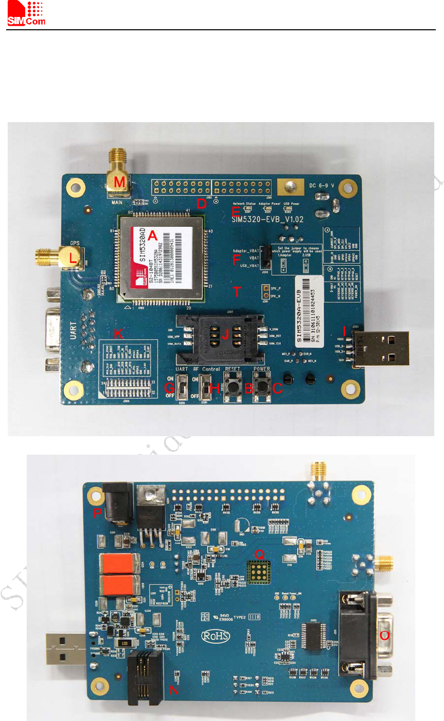
Figure 1: EVB view
A: SIM5320AD module
B: Reset keypad
C: Power on/off keypad
D: IO interface 1(including GPIO, ADC, SPI, etc)
E: LED indicator(including network status,operating status)
F: Power supply selection jumper
G: UART enable/disable switch
H: RF enable/disable (flight mode) switch
I: USB connector
J: SIM card socket
K: IO interface 2(including PCM,GPIO, UART, I2C, etc)
L: GPS antenna SMA
M: Main antenna SMA
O: UART connector
P: Adapter connector
Q: SIM5320AD JTAG test point
T: Speaker interface
All hardware Sub-interfaces included in SIM5320AD EVB are described in detail in following
chapters.
Smart Machine Smart Decision
SIM5320AD EVB User Guide 02.04.2011
7
3 EVB accessories
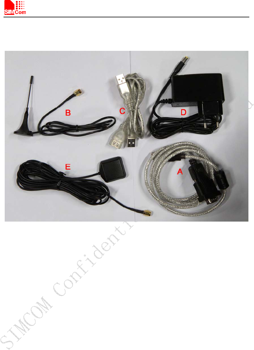
Figure 2: EVB accessory
A: USB to UART cable
B: RF antenna
C: USB cable
D: 6V DC adapter
E: GPS antenna
Smart Machine Smart Decision
SIM5320AD EVB User Guide 02.04.2011
8
4 Accessory Interface
4.1 Power Interface
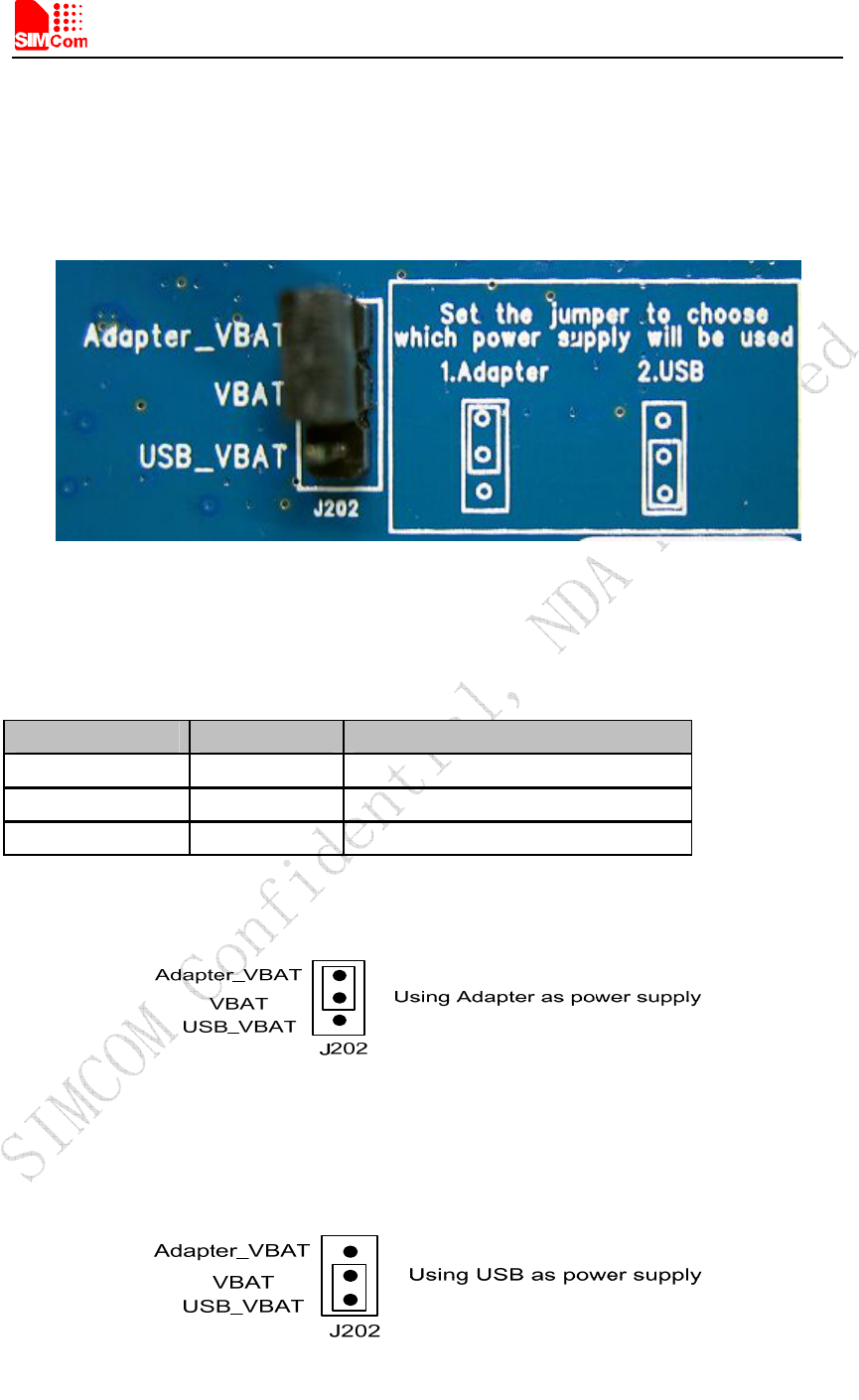
Figure 3: Power selection jumper
Table 2: Power supply
Signal Input/Output Description
Adapter_VBAT O 3.8V/2A DC source input
USB_VBAT O 3.8V/0.5A DC source input
VBAT I DC source input
If user wants to use DC adapter as power supply, Adapter_VBAT should be connected to VBAT
on J202 through a jumper as following figure shows.
This board could be powered by USB bus. User should connect the USB pin. USB_VBAT is the
USB power out.If user wants to use USB VBUS to power up the module, please connect
connector VBAT with connector USB_VBAT as following figure shows.and disconnect
Adapter_VBAT.
Smart Machine Smart Decision
SIM5320AD EVB User Guide 02.04.2011
9
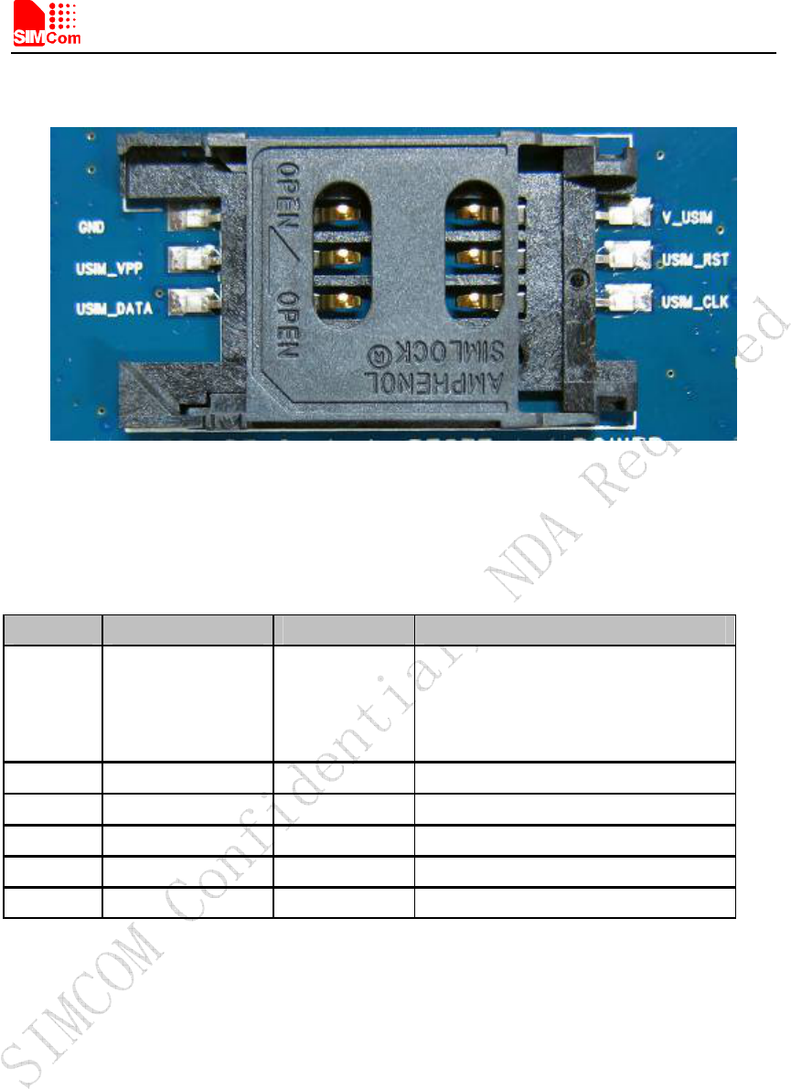
4.2 SIM card interface
Figure 4: SIM card socket
Table 3: SIM card socket
Pin Signal Input/Output Description
1
V_USIM O
USIM Card Power output automatic
output on USIM mode,one is
3.0V±10%, another is 1.8V±10%.
Current is about 10mA.
2 USIM_RESET O USIM Card Reset
3 USIM_CLK O USIM Card Clock
4 GND Ground
5 SIM_VPP O V_USIM
6 USIM_DATA I/O USIM Card data I/O
Smart Machine Smart Decision
SIM5320AD EVB User Guide 02.04.2011
10
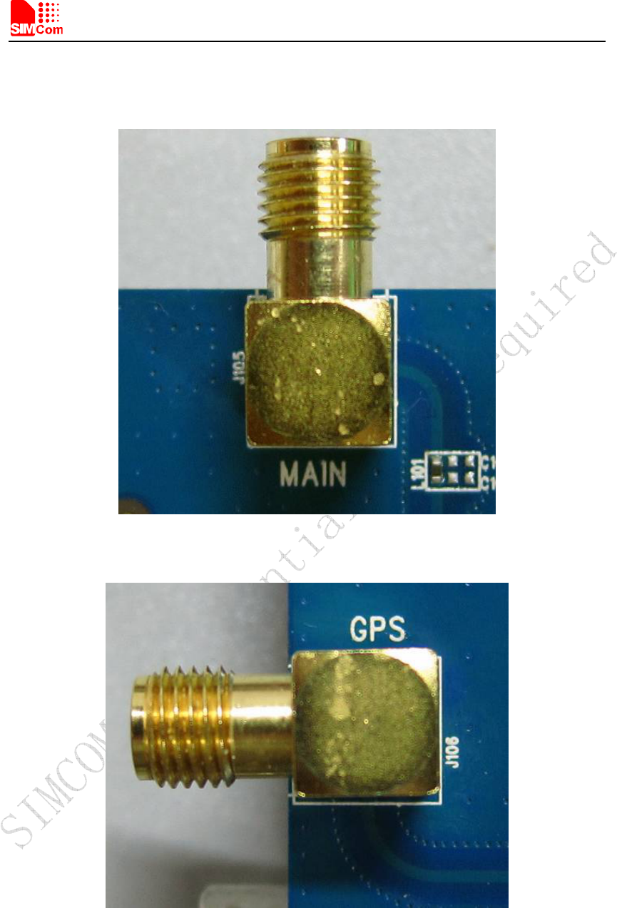
4.3 Antenna Interface
Figure 5: Main Antenna connector
Figure 6: GPS Antenna connector
Smart Machine Smart Decision
SIM5320AD EVB User Guide 02.04.2011
11
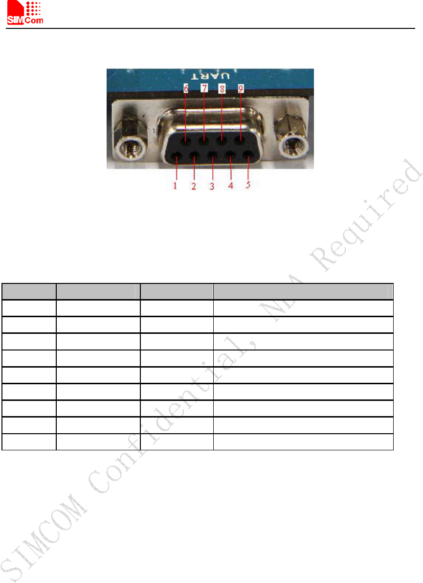
4.4 RS232 Interface
Figure 7: Serial Port
J205 is 9 pins standard RS232 UART interface. It can be connected to a PC directly.
Table 4: Serial Interface
Pin Signal I/O Description
1 DCD O Data carrier detection
2 TXD O Transmit data
3 RXD I Receive data
4 DTR I Data Terminal Ready
5 GND Ground
6 NC NC
7 RTS I Request to Send
8 CTS O Clear to Send
9 RI O Ring Indicator
Smart Machine Smart Decision
SIM5320AD EVB User Guide 02.04.2011
12
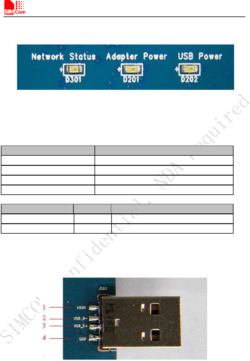
4.5 Operating Status LED
Figure 8: Status LED
Table 5: Network status LED
D301 Status Module Status
Off Module is not running
On Module is running, or voice call is connected
800ms On/ Off Module find the network and registered
200ms On/ Off Data communication
LED I/O Description
D201 O ADAPTER power indicator
D202 O USB power indicator
4.6 USB interface
Figure 9: USB Interface
It is a normal 4Pin USB connector.
Smart Machine Smart Decision
SIM5320AD EVB User Guide 02.04.2011
13
Table 6: USB interface
Pin Signal I/O Description
1 USB_VBUS I 5V
2 USB_DM I/O D+ line
3 USB_ DP I/O D- line
4 GND Ground
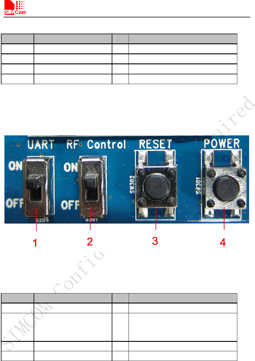
4.7 Switch interface
Figure 10: Switch Interface
Table 7: Switch interface
Switch Signal I/O Description
1 RS232 chip SHUTDOWN I UART switch
2 GPIO4 I RF switch (S301)
ON : Normal mode
OFF : Flight mode
3 RESET I Reset the module
4 PWRER_ON I Power on the module
Smart Machine Smart Decision
SIM5320AD EVB User Guide 02.04.2011
14
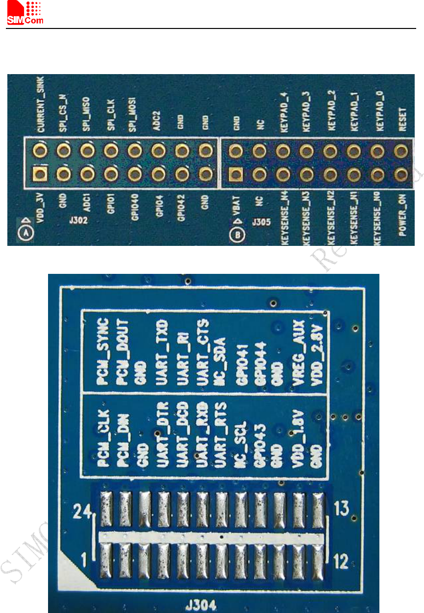
4.8 IO interface
Figure 11: IO Interface
Table 8: IO interface

Smart Machine Smart Decision
SIM5320AD EVB User Guide 02.04.2011
15
Signal I/O Description
GPIO40 I/O GPIO
POWER_ON I Power on the module
RESET I Reset the module
GPIO41 I/O GPIO
GPIO43 I/O GPIO
GPIO44 I/O GPIO
VDD_3V O 3V power supply
CURRENT_SINK I Current sink source
ADC1 I ADC
GPIO1 O Network status
GPIO4 I RF control switch
GPIO42 I/O GPIO
SPI_CS_N O SPI Chip selection
SPI_MISO I SPI Master input Slave output
SPI_MOSI O SPI Master output Slave input
ADC2 I ADC
KEYSENSE_N0 I Bit 0 for sensing key press on pad
matrix
KEYSENSE_ N1 I Bit 1 for sensing key press on pad
matrix
KEYSENSE_ N2 I Bit 2 for sensing key press on pad
matrix
KEYSENSE_ N3 I Bit 3 for sensing key press on pad
matrix
KEYSENSE_ N4 I Bit 4 for sensing key press on pad
matrix
KEYPAD_0 O Bit 0 drive to the pad matrix
KEYPAD_1 O Bit 1 drive to the pad matrix
KEYPAD_2 O Bit 2 drive to the pad matrix
KEYPAD_3 O Bit 3 drive to the pad matrix
KEYPAD_4 O Bit 4 drive to the pad matrix
I2C_SDA I/O I2C data
I2C_SCL O I2C clock
GPIO0 I General input pin for module wake up interrupt.
GPIO2 I General input pin.
GPIO3 O General output pin.
GPIO5 O General output pin.
Smart Machine Smart Decision
SIM5320AD EVB User Guide 02.04.2011
16
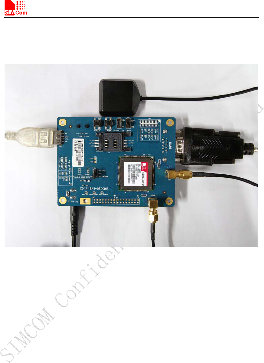
5 EVB and accessories
The EVB and its accessories are assembled as the figure below.
Figure 12: EVB and accessories

Smart Machine Smart Decision
SIM5320AD EVB User Guide 02.04.2011
17
6 Quickly start
6.1 Running
There are two ways to provide power supply to SIM5320AD module: one is to use the 6V power
supply provided in the EVB kit; the other is to use USB port of personal computer.
(1) When user use the power supply, if user insert 6V DC source adapter, user should connect
ADAPTER_VBAT pin and VBAT pin on the EVB board; then insert a valued SIM card and
check if the antenna is connected, and make sure that RF control switch is set to ON; finally
press the on/off switch for about 1 second, and then SIM5320AD module will begin running.
(2) Another option is to use USB port of Computer as power supply. To do so, user need to
connect USB_VBAT pin and VBAT pin on the EVB board, and make sure that RF control
switch is set to ON. Firstly insert the sim card and connect the antenna, then connect the PC
with USB-to-USB cable and press the Power_ON button for one second, then SIM5320AD
will start running.
User can see the light on the EVB flashing at a certain frequency about 1.25Hz. By the state,
user can judge whether the EVB and SIM5320AD is running or not. No function and test can be
executed if user has not connected necessary accessories.
NOTE: This EVB board supports USB power supply when user connects USB_VBAT and
VBAT together.
6.2 Installing Driver
There are 3 ways to connect the module to user’s computer and communicate via HyperTerminal:
(1) Using USB-TO-USB cable;
(2) Using UART-TO-USB cable;
(3) Using UART-TO-UART cable.
In the first case, user need install the module USB driver, which can be got from our FAE or sales;
For the UART to USB driver, user may get it from the CD in the EVB kit; If user use UART to
UART cable, there are certain points to be noticed. One can use UART to UART cable in EVB kit,
if the customers want to use their own UART to UART cable, please make sure that the pin
sequences of it is same as those of cable in EVB kit, pin sequences of which are shown in Figure
9.

Smart Machine Smart Decision
SIM5320AD EVB User Guide 02.04.2011
18
6.3 Connecting Net and calling
Once user installs the driver, user can follow steps below to connect to Network.
(1) When user use a UART-UART cable, user need to connect the serial port line to the serial port,
open the HyperTerminal (AT command windows) on user’s Personal computer. The location of
the HyperTerminal in windows2000/XP/Vista can be found from START→accessory→
communication→HyperTerminal. Please set the correct Baud Rate and COM port number, the
Baud Rate of SIM5320AD is 115200, and the COM port number is based on which UART port
user’s serial port line is inserted, user should select the port such as COM1 or COM2 etc.
(2) Connect the antenna to the SIM5320AD module using an antenna transmit line, insert SIM
card into the SIM card holder, and insert handset into its sockets.
(3) Follow the steps of running which has been mentioned above in Sector 5.1, power on the
system, type the AT command from the HyperTerminal, and then the SIM5320AD module will
execute its corresponding function. For example, if user type “AT”, then it should respond “OK”;
if user type “ATI”, it should display product identification information.
(4) If user want to use USB to USB cable, user need to connect the cable to USB port of the
module and the computer, then follow step 1~3.
(5) If user use UART to USB cable, user need to connect the cable to module serial port and the
USB port of the computer, then follow step 1~3.
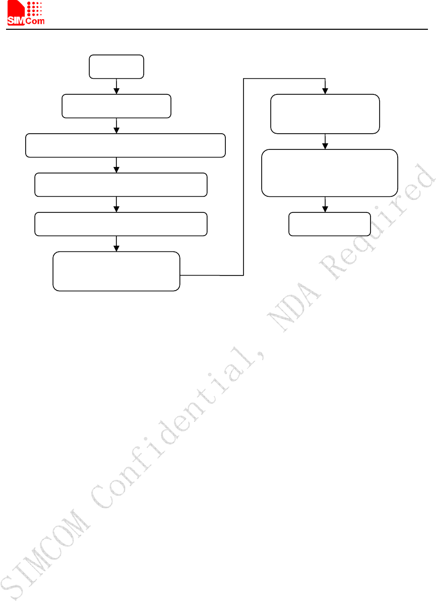
6.4 Downloading
Connect the USB port line to the USB port, connect the direct current source adapter, run the
download program, and choose the correct image, please follow the QDL downloading menu for
the operation. Update procedure is described in the figure below.
Smart Machine Smart Decision
SIM5320AD EVB User Guide 02.04.2011
19
Figure 13: USB interface update procedure
6.5 Turning off
Press the POWER_ON for about 1 second, SIM5320AD module will be turned off.
NOTE: If user uses USB to power on the module, just disconnect the USB cable to turn off.
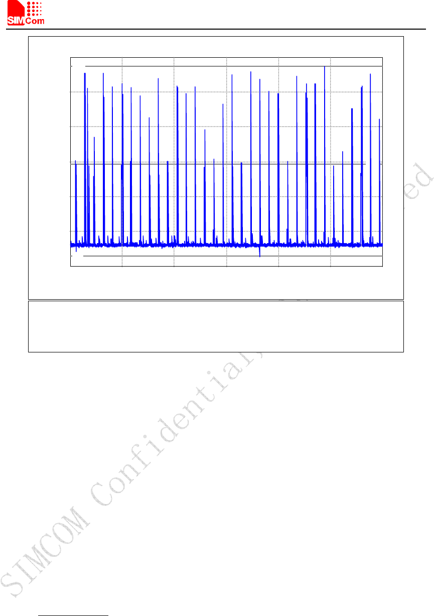
6.6 Measuring the current consumption
User can measure SIM5320AD current consumption in the sleep mode on our EVB. User need to
follow steps.
(1) Remove the jumper from J202, and provide a 3.8V DC power supply (such as: Agilent 66319B)
for VBAT on SIM5320AD EVB;
(2) Install a SIM card and a RF antenna;
(3) Shutdown UART by S204;
(4) Remove the USB cable;
(5) Power on SIM5320AD;
SIM5320AD will enter sleep mode automatically. User can measure SIM5320AD current
consumption. Test report is described in the figure below.
START
Module power on
Connect module USB slot and PC by USB cable
Install module driver on windows OS.
Close all app software which
use USB virtual
p
orts
Double click QDL.exe,
u
p
date be
g
in
Waiting until download finish,
QDL quit out automatically
Update success
Copy new firmware into QDL data folder
Smart Machine Smart Decision
SIM5320AD EVB User Guide 02.04.2011
20
Figure 14: current consumption in the sleep mode
Contact us:
Shanghai SIMCom Wireless Solutions Ltd.
Add: Building A,SIM Technology Building,No.633,Jinzhong Road,Changning
Disdrict,Shanghai P.R. China 200335
Tel: +86-21-3252 3300
Fax: +86-21-3252 3301
URL: www.sim.com
Current Waveform
Time
0.00s 4.00s 8.00s 12.00s 15.99s 19.99s 23.99s
Current (A)
-11.686m
8.511m
28.708m
48.904m
69.101m
89.298m
109.495m
High
Low
Max
Min
Calculated Measurements ( 170Hz sample rate)
Dc 3.2109mA Rms 12.8841mA
Low 750.2690uA Min -5.9155mA
High 47.2376mA Max 103.9990mA

Hardware Design
SIM5320AD_Hardware_Design
Smart Machine Smart Decision
Document Title SIM5320AD Hardware Design
Version 1.01
Date 2011-11-10
Status Release
Document Control ID SIM5320AD_Hardware Design_V1.01
General Notes
SIMCom offers this information as a service to its customers, to support application and engineering
efforts that use the products designed by SIMCom. The information provided is based upon requirements
specifically provided to SIMCom by the customers. SIMCom has not undertaken any independent search
for additional relevant information, including any information that may be in the customer’s possession.
Furthermore, system validation of this product designed by SIMCom within a larger electronic system
remains the responsibility of the customer or the customer’s system integrator. All specifications supplied
herein are subject to change.
Compliance Information
FCC Compliance Statement:
This device complies with Part 15 of the FCC Rules . Operation is subject to the following two conditions:
1. This device may not cause harmful interference, and
2. This device must accept any interference received, including
interference that may cause undesired operation. This device must accept any interference received,
including interference that may cause
undesired operation. Product that is a radio transmitter is labeled with FCC ID.
FCC Caution:
(1) Exposure to Radio Frequency Radiation. This equipment must be
installed and operated in accordance with provided instructions and the
antenna(s) used for this transmitter must be installed to provide a
separation distance of at least 20 cm from all persons and must not be collocated or operating in
conjunction with any other antenna or transmitter.
End-users and installers must be provided with antenna installation
instructions and transmitter operating conditions for satisfying RF exposure
compliance.
(2) Any changes or modifications not expressly approved by the grantee
of this device could void the user's authority to operate the equipment.
(3) This Transmitter must not be co-located or operating in conjunction with
any other antenna or transmitter.
(4) Changes or modifications to this unit not expressly approved by the
party responsible for compliance could void the user authority to operate
the equipment.

Smart Machine Smart Decision
SIM5320_Hardware Design_V1.01 2011-11-10
3
(1) the modules FCC ID is notvisible when installed in the host, or
(2) if the host is marketed so that end users do not havestraightforward commonly used methods
for access to remove the module so that the FCC ID ofthe module is visible; then an additional
permanent label referring to the enclosed module:Contains Transmitter Module
FCC ID: UDV-1103022011009
or Contains FCC ID: UDV-1103022011009 mustbe used.
Copyright
This document contains proprietary technical information which is the property of SIMCom Limited,
copying of this document and giving it to others and the using or communication of the contents thereof,
are forbidden without express authority. Offenders are liable to the payment of damages. All rights
reserved in the event of grant of a patent or the registration of a utility model or design. All specification
supplied herein are subject to change without notice at any time.
Copyright © Shanghai SIMCom Wireless Solutions Ltd. 2011

Smart Machine Smart Decision
SIM5320_Hardware Design_V1.01 2011-11-10
4
Contents
Revision History .......................................................................................................................................... 8
1 Introduction .......................................................................................................................................... 9
1.1 Product Outline................................................................................................................................ 9
1.2 Hardware Interface Overview.......................................................................................................... 9
1.3 Hardware Diagram........................................................................................................................... 9
1.4 Functional Overview...................................................................................................................... 10
2 Package Information...........................................................................................................................11
2.1 Pin Configuration............................................................................................................................11
2.2 Pin description ............................................................................................................................... 14
2.3 Package Dimensions...................................................................................................................... 16
2.4 Footprint Recommendation ........................................................................................................... 18
3 Application Interface Specification................................................................................................... 18
3.1 Power Supply................................................................................................................................. 18
3.1.1 Power Supply Pin.................................................................................................................... 19
3.1.2 Design Guide .......................................................................................................................... 19
3.1.3 RTC Backup............................................................................................................................ 21
3.2 Power on/off Time Sequence ......................................................................................................... 23
3.2.1 Power on Sequence ................................................................................................................. 23
3.2.2 Power off Sequence ................................................................................................................ 25
3.3 UART Interface.............................................................................................................................. 26
3.3.1 Pin Description........................................................................................................................ 27
3.3.2 Application Guide................................................................................................................... 28
3.4 USIM Interface .............................................................................................................................. 29
3.4.1 Pin description ........................................................................................................................ 29
3.4.2 Application Guide................................................................................................................... 30
3.4.3 Recommend Components ....................................................................................................... 30
3.5 I2C Interface .................................................................................................................................. 31
3.5.1 Pin Description........................................................................................................................ 32
3.5.2 Signal Description................................................................................................................... 32
3.5.3 Design Guide .......................................................................................................................... 32
3.6 USB Interface ................................................................................................................................ 32
3.6.1 Application Guide................................................................................................................... 33
3.7 SPI Interface .................................................................................................................................. 33
3.7.1 Pin Description........................................................................................................................ 33
3.8 GPIO Interface............................................................................................................................... 34
3.8.1 Pin Description........................................................................................................................ 34
3.8.2 Application Guide................................................................................................................... 35
3.9 Global Positioning System............................................................................................................. 37
3.9.1 Technical specification............................................................................................................ 37
3.9.2 Operate Mode.......................................................................................................................... 37
3.9.3 Application Guide................................................................................................................... 38

Smart Machine Smart Decision
SIM5320_Hardware Design_V1.01 2011-11-10
5
3.10 Multi-functional interface........................................................................................................... 39
3.10.1 Sink Current Source ............................................................................................................ 39
3.10.2 Reset Function..................................................................................................................... 40
3.10.3 ADC..................................................................................................................................... 40
3.10.4 LDO..................................................................................................................................... 41
4 RF Specification.................................................................................................................................. 42
4.1 RF Specification ............................................................................................................................ 42
4.2 Operating Specification ................................................................................................................. 43
4.3 Antenna Design Guide................................................................................................................... 44
5 Reliability and Operating Characteristics........................................................................................ 45
5.1 Electronic Characteristics .............................................................................................................. 45
5.2 Operating Mode ............................................................................................................................. 45
5.2.1 Operating Modes Overview.................................................................................................... 46
5.2.2 Minimize Power Consumption ............................................................................................... 46
5.3 Current Consumption..................................................................................................................... 47
5.4 EMC and ESD Notes ..................................................................................................................... 49
6 Guide for Production.......................................................................................................................... 50
6.1 Top and Bottom View of SIM5320AD ......................................................................................... 50
6.2 Typical Solder Reflow Profile ....................................................................................................... 50
6.3 Moisture Sensitivity Level (MSL)................................................................................................. 51
6.4 Stencil Foil Design Recommendation ........................................................................................... 51
6.5 Recommended Pad Design ............................................................................................................ 51
Appendix .................................................................................................................................................... 52
A. System Design..................................................................................................................................... 52
B. SIM5320AD GPIOs List ..................................................................................................................... 53
C. Digital I/O Characteristics................................................................................................................... 53
D. Related Documents ............................................................................................................................. 54
E. Terms and Abbreviations..................................................................................................................... 55
F. Safety Caution...................................................................................................................................... 58

Smart Machine Smart Decision
SIM5320_Hardware Design_V1.01 2011-11-10
6
Table Index
Table 1: General Feature ................................................................................................................................................. 10
Table 2: Pin definition..................................................................................................................................................... 13
Table 3: Pin description................................................................................................................................................... 14
Table 4: Pin description................................................................................................................................................... 19
Table 5: Power on timing ................................................................................................................................................ 24
Table 6: Power off timing ............................................................................................................................................... 26
Table 7: Pin description................................................................................................................................................... 27
Table 8: Logic level ........................................................................................................................................................ 28
Table 9: Electronic characteristic .................................................................................................................................... 29
Table 10: Pin description................................................................................................................................................. 29
Table 11:: Amphenol USIM socket pin description......................................................................................................... 31
Table 12: Pin description................................................................................................................................................. 32
Table 13: Electronic characteristic .................................................................................................................................. 32
Table 14: Electronic characteristic .................................................................................................................................. 33
Table 15: Pin description................................................................................................................................................. 34
Table 16: Electronic characteristic .................................................................................................................................. 34
Table 17: Pin description................................................................................................................................................. 35
Table 18: LED status....................................................................................................................................................... 36
Table 19: Control status .................................................................................................................................................. 36
Table 20: Electronic characteristic .................................................................................................................................. 39
Table 21: Electronic Characteristics................................................................................................................................ 41
Table 22: Electronic characteristic .................................................................................................................................. 41
Table 23: Conducted transmission power ....................................................................................................................... 42
Table 24: Operating frequencies ..................................................................................................................................... 42
Table 25: Conducted receive sensitivity.......................................................................................................................... 42
Table 26: GPRS/EDGE data throughout ......................................................................................................................... 43
Table 27: HSDPA throughout.......................................................................................................................................... 43
Table 28: Absolute maximum ratings.............................................................................................................................. 45
Table 29: Recommended operating ratings ..................................................................................................................... 45
Table 30: Operating temperature..................................................................................................................................... 45
Table 31: Operating Modes Overview ............................................................................................................................ 46
Table 32: Current consumption....................................................................................................................................... 47
Table 33: The ESD performance measurement table (Temperature: 25℃, Humidity: 45%) .......................................... 49
Table 34: SIM5320AD GPIOs list .................................................................................................................................. 53
Table 35: Digital I/O characteristics................................................................................................................................ 53
Table 36: Related documents .......................................................................................................................................... 54
Table 37: Terms and Abbreviations................................................................................................................................. 55
Table 38: Safety caution.................................................................................................................................................. 58

Smart Machine Smart Decision
SIM5320_Hardware Design_V1.01 2011-11-10
7
Figure Index
Figure 1: SIM5320AD functional architecture................................................................................................................ 10
Figure 2: Pin view........................................................................................................................................................... 12
Figure 3: Top dimensions (Unit: mm)............................................................................................................................. 16
Figure 4: Side dimensions (Unit: mm)............................................................................................................................ 17
Figure 5: Bottom dimensions (Unit: mm) ....................................................................................................................... 17
Figure 6: Footprint recommendation (Unit: mm)............................................................................................................ 18
Figure 7: VBAT_RF voltage drop during burst emission (GSM/GPRS)......................................................................... 19
Figure 8: VBAT input application circuit........................................................................................................................ 20
Figure 9: Reference circuit of the LDO power supply .................................................................................................... 20
Figure 10: Reference circuit of the DCDC power supply ............................................................................................... 21
Figure 11: RTC supply from capacitor............................................................................................................................ 22
Figure 12: RTC supply from non-chargeable battery...................................................................................................... 22
Figure 13: RTC supply from rechargeable battery .......................................................................................................... 22
Figure 14: Seiko XH414H-IV01E Charge-Discharge characteristic............................................................................... 23
Figure 15: Power on Timing Sequence ........................................................................................................................... 24
Figure 16: Application circuit ......................................................................................................................................... 25
Figure 17: Power off timing sequence ............................................................................................................................ 26
Figure 18: Full modem.................................................................................................................................................... 27
Figure 19: Null modem ................................................................................................................................................... 27
Figure 20: RI behaviour in NULL Modem ..................................................................................................................... 28
Figure 21: RI behaviour in FULL Modem ...................................................................................................................... 29
Figure 22: USIM interface reference circuit ................................................................................................................... 30
Figure 23: Amphenol SIM card socket ........................................................................................................................... 31
Figure 24: USB interface ................................................................................................................................................ 33
Figure 25: Application circuit ......................................................................................................................................... 35
Figure 26: Flight mode switch ........................................................................................................................................ 36
Figure 27: Active antenna circuit .................................................................................................................................... 38
Figure 28:Passive antenna circuit (Default) ................................................................................................................. 38
Figure 29: Current drive.................................................................................................................................................. 40
Figure 30: Reset circuit................................................................................................................................................... 40
Figure 31: Reference circuit............................................................................................................................................ 41
Figure 32: Antenna matching circuit............................................................................................................................... 44
Figure 33: Top and bottom view of SIM5320AD ........................................................................................................... 50
Figure 34: The ramp-soak-spike reflow profile of SIM5320AD..................................................................................... 50
Figure 35: Recommended pad ........................................................................................................................................ 51
Figure 36: System design................................................................................................................................................ 52

Smart Machine Smart Decision
SIM5320_Hardware Design_V1.01 2011-11-10
8
Revision History
Data Version Description of change Author
2011-11-10 1.01 Original Libing

Smart Machine Smart Decision
SIM5320_Hardware Design_V1.01 2011-11-10
9
1 Introduction
This document describes electronic specifications, RF specifications, function interface, mechanical
characteristic and testing conclusions of the SIMCom SIM5320AD module. With the help of this
document and other SIM5320AD software application notes, user guides, users can quickly understand
and use SIM5320AD module to design and develop applications quickly.
1.1 Product Outline
Designed for global market, SIM5320AD is a quad-band GSM/GPRS/EDGE and dual-band UMTS
/HSDPA that works on frequencies of GSM 850MHz, EGSM 900 MHz, DCS 1800 MHz, PCS 1900MHz
and WCDMA 1900/850MHz. The SIM5320 support HSDPA.User can choose the module based on the
wireless network configuration.
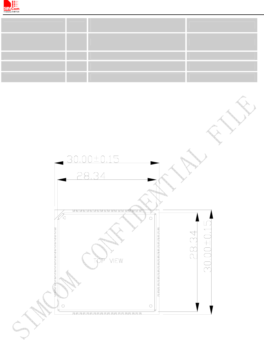
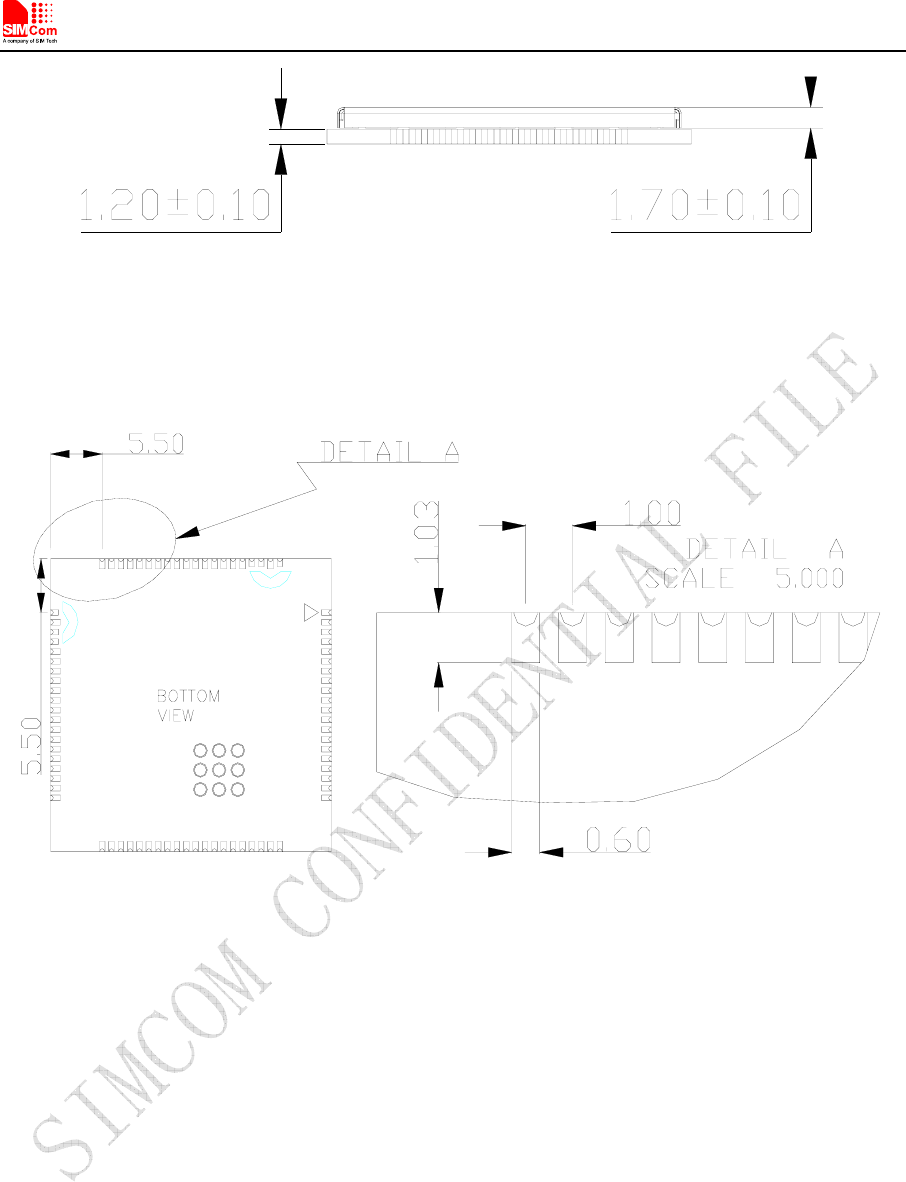
With a tiny configuration of 30*30*2.9 mm and integrated functions, SIM5320AD can meet almost any
space requirement in users’ application, such as Smart phone, PDA phone, industrial handhelds,
machine-to-machine, vehicle applications, etc..
There are 80 pins on SIM5320AD, which provide most application interfaces for customers’ board.
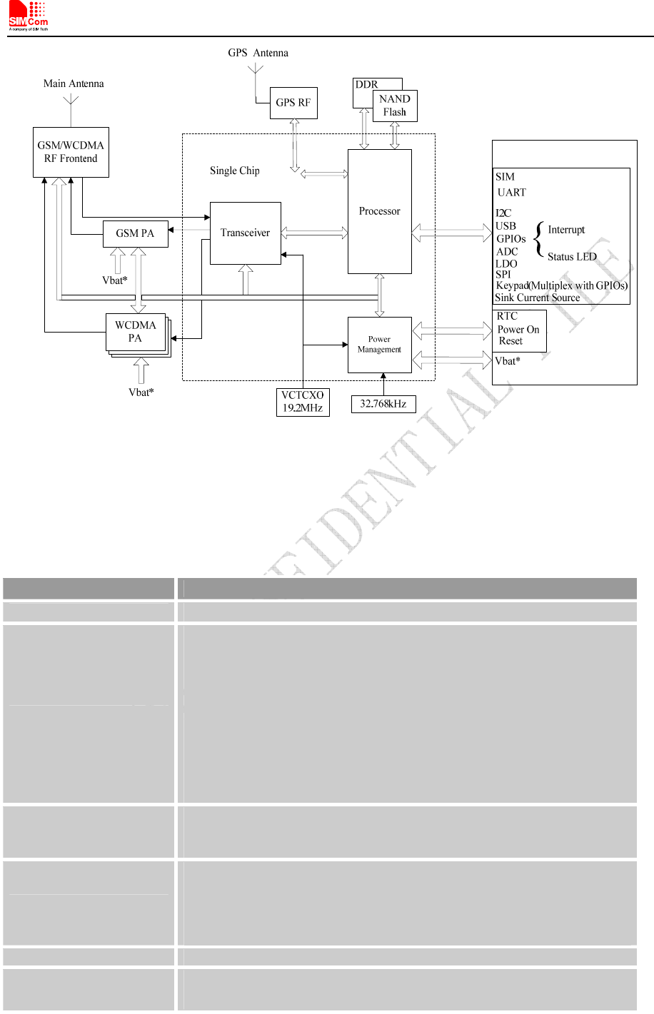
1.2 Hardware Interface Overview
Sub-interfaces are described in detail in the next chapter, which includes:
● Power Supply
● USB Interface
● Serial Interface
● SIM Interface
● GPIO
● ADC
● LDO Power Output
● Sink Current Source
● Keypad Interface
● SPI Interface
● RTC
● I2C Interface
1.3 Hardware Diagram
The global architecture of the SIM5320AD Embedded module is described in the figure below.
Smart Machine Smart Decision
SIM5320_Hardware Design_V1.01 2011-11-10
10
Figure 1: SIM5320AD functional architecture
1.4 Functional Overview
Table 1: General Feature
Feature Implementation
Power supply Single supply voltage 3.3~4.2V
Transmission data
● Dual-mode UMTS/HSDPA/EDGE/GPRS operation
● GPRS Class B, multislot class 12 operation, Supports coding scheme:
CS1-4
● EDGE multislot class 12 operation, Supports coding schemes
MSC1-9
● UMTS R99 data rates-384 kbps DL/UL
● HSDPA Category 5/6 -3.6 Mbps Category12-1.8 Mbps
● CSD feature: 9.6, 14.4, 64 kbps UL/DL
GPS
● Mobile-Assisted mode
● Mobile-based mode
● Standalone mode
SMS
● MT, MO, CB, Text and PDU mode
● SMS storage: SIM card
● Support transmission of SMS alternatively over CSD or GPRS.
User can choose preferred mode.
SIM interface Support identity card: 1.8V, 3V.
Serial interface ● Serial Port standard or null modem mode on Serial Port Interface
● Serial Port can be used to control module by sending AT command

Smart Machine Smart Decision
SIM5320_Hardware Design_V1.01 2011-11-10
11
USB Support USB2.0 Slave mode
Phonebook management Support phonebook types: SM, FD, LD, RC, ON, MC.
SIM application toolkit Support SAT class 3, GSM 11.14 Release 98
Support USAT
Real Time Clock Support RTC
Timer function Programmable by AT command
Physical characteristics Size:30*30*2.9mm
Weight:5.6g
Firmware upgrade Firmware upgrade over USB interface
Temperature range ● Operation temperature: -30°C to +80°C
● Storage temperature -40°C to +85°C
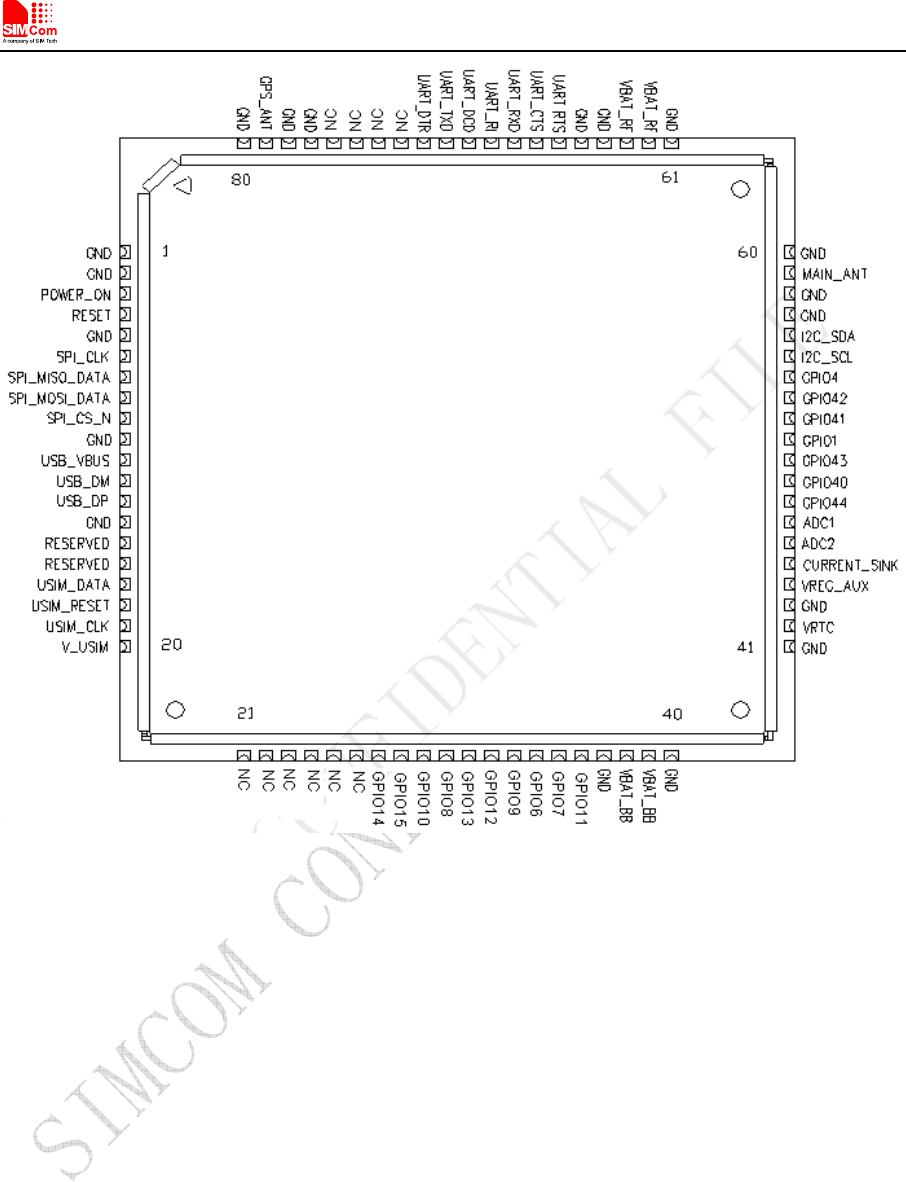
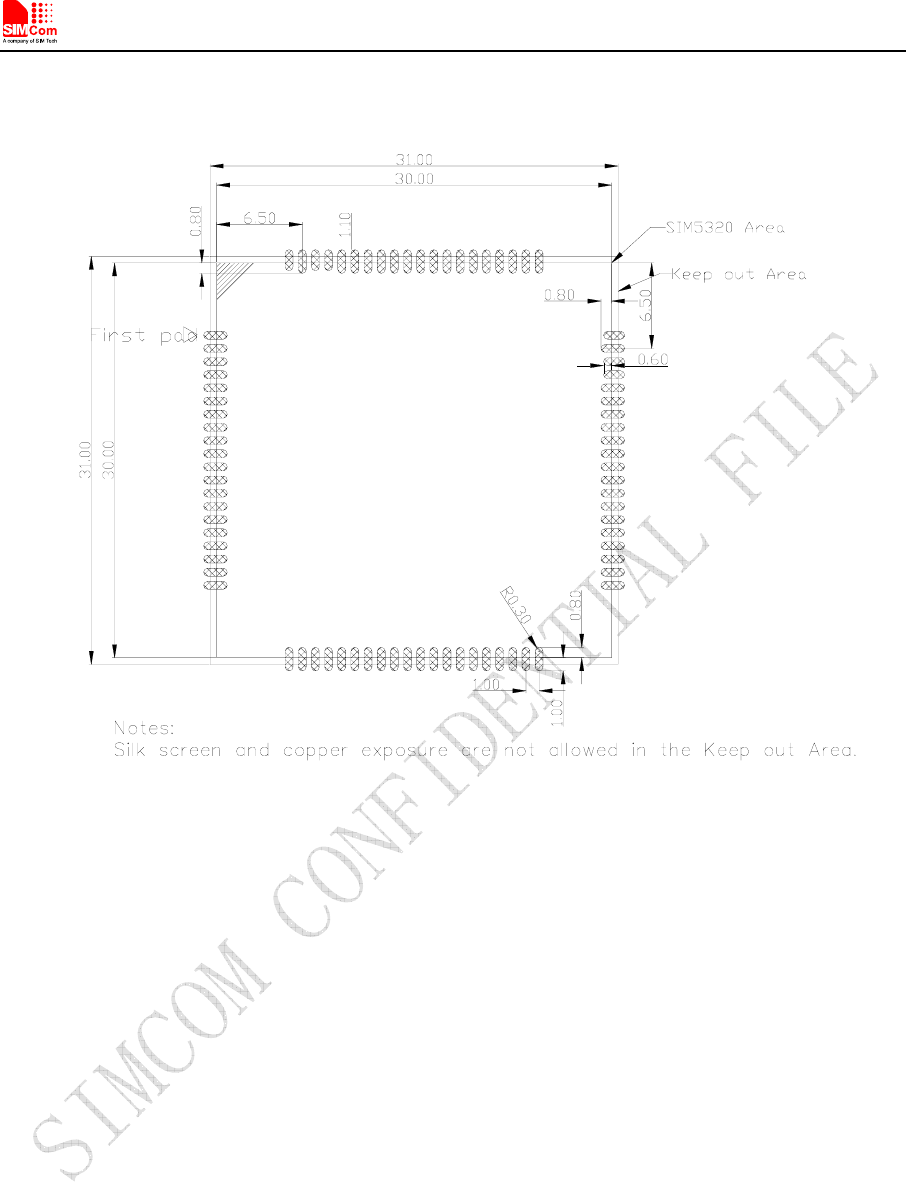
2 Package Information
2.1 Pin Configuration
All hardware interfaces which connect SIM5320AD to customers’ application platform are through 80
pins pads (Metal half hole). Figure 2 is SIM5320AD outline diagram.
Smart Machine Smart Decision
SIM5320_Hardware Design_V1.01 2011-11-10
12
Figure 2: Pin view

Smart Machine Smart Decision
SIM5320_Hardware Design_V1.01 2011-11-10
13
Table 2: Pin definition
Pin No. Define Pin No. Define
1 GND 2 GND
3 POWER_ON 4 RESET
5 GND 6 SPI_CLK
7 SPI_MISO_DATA 8 SPI_MOSI_DATA
9 SPI_CS_N 10 GND
11 USB_VBUS 12 USB_DM
13 USB_DP 14 GND
15 RESERVED 16 RESERVED
17 USIM_DATA 18 USIM_RESET
19 USIM_CLK 20 V_USIM
21 NC 22 NC
23 NC 24 NC
25 NC 26 NC
27 GPIO14 28 GPIO15
29 GPIO10 30 GPIO8
31 GPIO13 32 GPIO12
33 GPIO9 34 GPIO6
35 GPIO7 36 GPIO11
37 GND 38 VBAT_BB
39 VBAT_BB 40 GND
41 GND 42 VRTC
43 GND 44 VREG_AUX
45 CURRENT_SINK 46 ADC2
47 ADC1 48 GPIO44
49 GPIO40 50 GPIO43
51 GPIO1 52 GPIO41
53 GPIO42 54 GPIO4
55 I2C_SCL 56 I2C_SDA
57 GND 58 GND
59 MAIN_ANT 60 GND
61 GND 62 VBAT_RF
63 VBAT_RF 64 GND
65 GND 66 UART_RTS
Smart Machine Smart Decision
SIM5320_Hardware Design_V1.01 2011-11-10
14
67 UART_CTS 68 UART_RXD
69 UART_RI 70 UART_DCD
71 UART_TXD 72 UART_DTR
73 NC 74 NC
75 NC 76 NC
77 GND 78 GND
79 GPS_ANT 80 GND
2.2 Pin description
Table 3: Pin description
Pin name I/O Description Comment
Power Supply
VB AT_ RF/ VB AT_B B Power supply voltage
VRTC I/O Power supply for RTC
VREG_AUX O LDO power output
If it is unused, keep open.
GND Ground
Power on/off
POWER_ON I
POWER_ON should be pulled low at
least 64ms to power on or 500ms to
power off the module.
USIM interface
V_USIM O Voltage Supply for SIM card
Support 1.8V or 3V SIM card
USIM_DATA I/O SIM Data Output/Input
USIM_CLK O SIM Clock
USIM_RESET O SIM Reset
All signals of SIM
interface should be
protected against
ESD/EMC.
SPI interface
SPI_CLK O SPI clock
SPI_CS_N O SPI chip-select
SPI_MOSI_DATA O SPI (master only) master out/slave in
data
SPI_MISO_DATA I SPI (master only) master in/slave out
data
If it is unused, keep open.
USB
USB_VBUS I USB power supply input They are compliant with

Smart Machine Smart Decision
SIM5320_Hardware Design_V1.01 2011-11-10
15
USB_DP I/O
Plus (+) line of the differential,
bi-directional USB signal to/from the
p
eri
p
heral device.
USB_DM I/O
Minus (-) line of the differential,
bi-directional USB signal to/from the
p
eri
p
heral device.
Serial interface
UART_RXD I Receive Data
UART_TXD O Transmit Data
UART_RTS O Request to send
UART_CTS I Clear to Send
UART_RI O Ring Indicator
UART_DTR I/O DTE get ready
UART_DCD O Carrier detects
UART_RXD has been
pulled down with a 12kR
resistor to ground in the
module.
If it is unused, keep open.
I2C interface
I2C_SDA I/O I2C data
I2C_SCL O I2C clock output
Pulled up with a 2.2kR
resistor to 2.6V internally.
If it is unused, keep open.
GPIOs
GPIO6 I/O General input/output PIN.
GPIO7 I/O General input/output PIN.
GPIO8 I/O General input/output PIN.
GPIO9 I/O General input/output PIN.
GPIO10 I/O General input/output PIN.
GPIO11 I/O General input/output PIN.
GPIO12 I/O General input/output PIN.
GPIO13 I/O General input/output PIN.
GPIO14 I/O General input/output PIN.
GPIO15 I/O General input/output PIN.
All GPIOs.are 1.8V.
If it is unused, keep open.
GPIO1 O Output PIN as LED control for
network status.
GPIO4 I Input PIN as RF operating control.
GPIO40 O Output PIN as operating status
indicating of module.
GPIO41 I/O
General input/output PIN. It can be
used as wake/interrupt signal to host
from module
GPIO43 I/O
General input/output PIN. It can be
used as wake/interrupt signal to
module from host.
GPIO44 I/O General input/output PIN.
GPIO42 I/O General input/output PIN.
If it is unused, keep open.
Other interface
RESET I System reset in, active low.
Smart Machine Smart Decision
SIM5320_Hardware Design_V1.01 2011-11-10
16
CURRENT_SINK I Current source of ground-referenced
current sink Refer to 3.10
ADC1 I Analog Digital Converter Input Refer to 3.10
ADC2 I Analog Digital Converter Input
MAIN_ANT I/O ANT soldering pad
GPS_ANT I/O GPS ANT soldering pad
2.3 Package Dimensions
The following figure shows mechanical dimensions of SIM5320AD.
Figure 3: Top dimensions (Unit: mm)
Smart Machine Smart Decision
SIM5320_Hardware Design_V1.01 2011-11-10
17
Figure 4: Side dimensions (Unit: mm)
Figure 5: Bottom dimensions (Unit: mm)
Smart Machine Smart Decision
SIM5320_Hardware Design_V1.01 2011-11-10
18
2.4 Footprint Recommendation
Figure 6: Footprint recommendation (Unit: mm)
3 Application Interface Specification
3.1 Power Supply
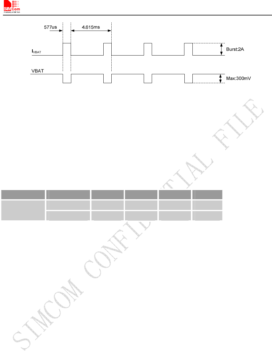
The power supply pins of SIM5320AD include VBAT_RF and VBAT_BB. VBAT_RF directly supplies
the power to RF PA; VBAT_BB supplies the power to the baseband system. For the VBAT_RF, the ripple
due to GSM/GPRS emission burst (every 4.615ms)may cause voltage drop, and the current consumption
rises typically to peak of 2A. So the power supply must be able to provide sufficient current up to 2A. The
following figure is the VBAT_RF voltage ripple wave at the maximum power transmit phase.
The test condition: VBAT_RF=4.0V, VBAT maximum output current =2A, CA=100 µF tantalum capacitor
(ESR=0.7Ω) and CB=1µF(Please refer to Figure 36—Application circuit).
Smart Machine Smart Decision
SIM5320_Hardware Design_V1.01 2011-11-10
19
Figure 7: VBAT_RF voltage drop during burst emission (GSM/GPRS)
3.1.1 Power Supply Pin
Two VBAT_RF and two VBAT_BB pins are dedicated to connect the supply voltage.
Table 4: Pin description
Pin type Pin name Min Typ Max Unit
VBAT_RF 3.3 3.8 4.2 V
POWER
VBAT_BB 3.3 3.8 4.2 V
Note: 1.Though the VBAT_RF and VBAT_BB are supplied by the same voltage level, they are different pins. VBAT_RF
is for RF section and VBAT_BB is for baseband system.
2. When the module is power off, users must pay attention to the issue about current leakage. Refer to Chapter 3.10.2
Note2.
3.1.2 Design Guide
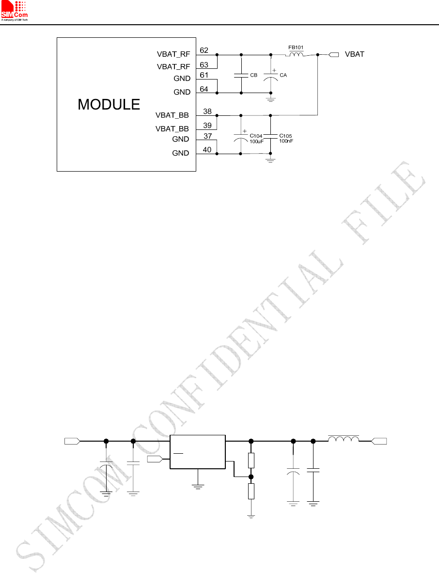
Mostly, user connects the VBAT_RF and VBAT_BB pins with one power supply. Make sure that the input
voltage at the VBAT_BB pin will never drop below 3.3V even during a transmit burst when the current
consumption rises up to 2A. If the power voltage drops below 3.3V, the module may be shut down
automatically. Using a large tantalum capacitor (above 100uF) will be the best way to reduce the voltage
drops. If the power current cannot support up to 2A, users must introduce larger capacitor (typical 1000uF)
to storage electric power, especially GPRS multiple time slots emission.
For the consideration of RF performance and system stability, another large capacitor (above 100uF)
should be located at the VBAT_RF pin and some multi-layer ceramic chip (MLCC) capacitors (0.1uF)
need to be used for EMC because of their low ESR in high frequencies. Note that capacitors should be put
beside VBAT_RF pins as close as possible. Also User should minimize the PCB trace impedance from the
power supply to the VBAT pins through widening the trace to 80 mil or more on the board. The following
figure is the recommended circuit.
Smart Machine Smart Decision
SIM5320_Hardware Design_V1.01 2011-11-10
20
Figure 8: VBAT input application circuit
There are three sections about how to design and optimize users’ power systems.
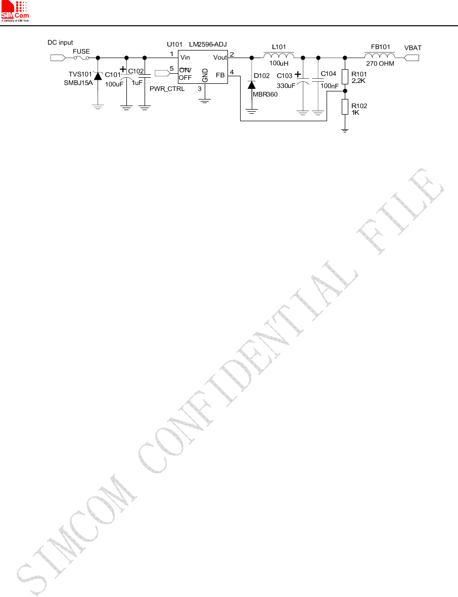
Power supply circuit
We recommend DCDC or LDO is used for the power supply of the module, make sure that the peak
current of power components can rise up to 2A. The following figure is the reference design of +5V input
power supply. The designed output for the power supply is 4.1V, here a linear regulator can be used.
Vin Vout
ON/
OFF
GND
FB
3
+
PWR_CTRL
R102
R101
FB101 VBAT
100K
43K
270 OHM
+C103
330uF
C104
100nF
U101 MIC29302
5
4
1
2
C101 C102
100uF 1uF
DC INPUT
Figure 9: Reference circuit of the LDO power supply
If there is a big difference between the input voltage and the desired output (VBAT), a switching converter
power will be preferable because of its better efficiency, especially at the high current situation. The
following figure is the reference circuit. Note that DCDC may deprave RF performance because of ripple
current intrinsically.
Smart Machine Smart Decision
SIM5320_Hardware Design_V1.01 2011-11-10
21
Figure 10: Reference circuit of the DCDC power supply
Voltage monitor
To monitor the power supply voltage, user can use the AT command “AT+CBC”, this command has two
parameters: the battery status and the voltage value (mV). It will return the capacity percentage and actual
value of battery (at the VBAT_BB pin). The voltage is continuously measured at intervals, whenever the
measured battery voltage is lower than a specific value set by the AT command “AT+CVALARM”. For
example, if the voltage value is set to be 3.4V, the following URC will be presented: “warning! voltage is
low: 3.3v”.
If the voltage is lower than a specific value which is set by the AT command “AT+CPMVT”, the module
will be powered off automatically and AT commands cannot be executed any more.
Note: Under-voltage warning function is disabled by default, user can enable it by the AT command “AT+CVALARM”.
Auto power off feature is disabled by default, user should set it by the AT command “AT+CPMVT” to an appropriate
value. Please refer to Document [1].
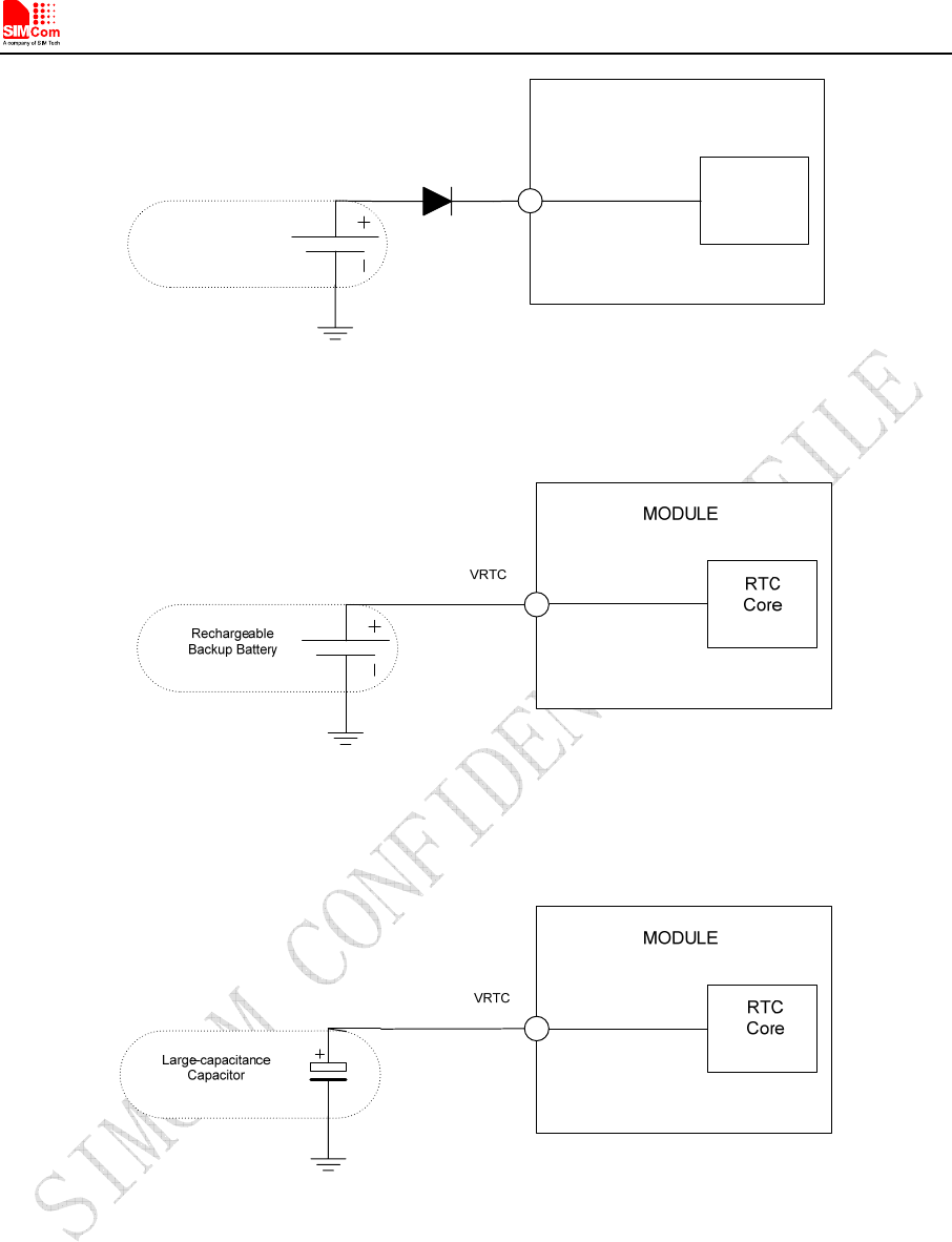
3.1.3 RTC Backup
The module uses RTC (Real Time Clock) to update and maintain inherent time and keeps system alive at
no power supply status. The RTC power supply of module can be provided by an external capacitor or a
battery (non-chargeable or rechargeable) through the VRTC. The following figures show various reference
circuits for RTC back up. The discharge current is less than 10uA. If this feature is used, please refer to the
AT commands “AT+CTZU” and “AT +CTZR”.
z External capacitor backup
Smart Machine Smart Decision
SIM5320_Hardware Design_V1.01 2011-11-10
22
RTC
Core
MODULE
VRTC
Non-chargeable
Backup Battery
Figure 11: RTC supply from capacitor
z Non-chargeable battery backup
Figure 12: RTC supply from non-chargeable battery
z Rechargeable battery backup
Figure 13: RTC supply from rechargeable battery
Note: The VRTC can be disabled, jus disconnect it in application circuit.
Coin-type rechargeable battery is recommended, such as XH414H-IV01E form Seiko can be used.
Typical charge-discharge curves for this battery are shown in the following figure.

Smart Machine Smart Decision
SIM5320_Hardware Design_V1.01 2011-11-10
23
Figure 14: Seiko XH414H-IV01E Charge-Discharge characteristic
3.2 Power on/off Time Sequence
3.2.1 Power on Sequence
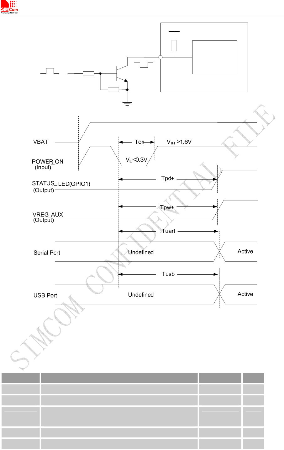
SIM5320AD can be powered on by POWER_ON pin, which starts normal operating mode.
POWER_ON pin is pulled up with a 200kR resistor to 1.8V in module. User can power on the
SIM5320AD by pulling the POWER_ON pin down for a short time. The power-on scenarios are
illustrated in the following figures.
Smart Machine Smart Decision
SIM5320_Hardware Design_V1.01 2011-11-10
24
4.7 K
47K
Turn on/ off impulse
POWER_ON
Power
on / off logic
200K
1.8V
MODULE
Figure 15: Power on Timing Sequence
Table 5: Power on timing
Parameter Description Time value Unit
Ton The time to pull POWER_ON down to power on 64< Ton<180 ms
TpD+ The time to indicate connecting with the network >5.5 s
Tpw+ The time to indicate the module is powered on
completely >4.5 s
Tuart The time to enable UART >4.7 s
Tusb The time to enable USB >9 s
Smart Machine Smart Decision
SIM5320_Hardware Design_V1.01 2011-11-10
25
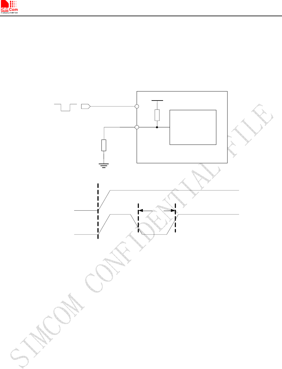
Automatic power on
If user needs to power on SIM5320AD automatically whenever the VBAT pins are connected to the power
supply, then POWER_ON pin is just pulled to ground by a resistance in circuit directly. The following is
the reference circuit.
10 K
POWER _ON
Power
on /off logic
200K
1.8V
MODULE
R1
RESET
Reset impulse
V
IL
<0. 3V
50ms<t<200ms
VBAT
RESET
( Input)
Figure 16: Application circuit
Note: After automatically powering on the module by pulling down POWER_ON pin to ground anytime, USB/UART may
not communicate normally with host, so it is suggested that SIM5320AD should be reset by RESET pin.
3.2.2 Power off Sequence
The following methods can be used to power down SIM5320AD. These procedures will make module
disconnect from the network and allow the software to enter a safe state, and then save data before
completely powering the module off.
● Method 1: Power off SIM5320AD by pulling the POWER_ON pin down
● Method 2: Power off SIM5320AD by AT command
User can power off the SIM5320AD by pulling POWER_ON down for a specific time. The power off
scenario is illustrated in the following figure.

Smart Machine Smart Decision
SIM5320_Hardware Design_V1.01 2011-11-10
26
Figure 17: Power off timing sequence
Table 6: Power off timing
Parameter Description Time value Unit
Toff The time pulling POWER_ON down to power off 0.5< Toff<5 s
TpD- The time to indicate disconnecting from the network >7 s
Tpw- The time to indicate the module power off completely >7.5 s
Tuart_off The time to disable UART >6 s
Tusb_off The time to disable USB >7.5 s
User can also use the AT command “AT + CP O F” to power down the module. After that, the AT commands
cannot be executed any longer. The module enters the POWER DOWN mode, only the RTC is still active.
For details, refer to Document [1].
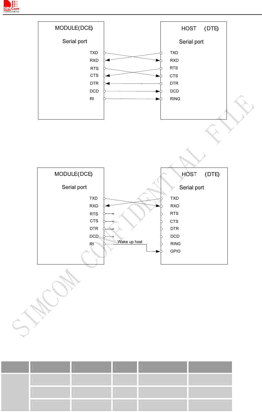
3.3 UART Interface
SIM5320AD provides a UART (universal asynchronous serial transmission) port. It consists of a flexible
7-wire serial interface. The module is as the DCE (Data Communication Equipment) and the client PC is
as the DTE (Data Terminal Equipment). AT commands are entered and serial communication is performed
through UART interface. The application circuit is in the following figures.
Smart Machine Smart Decision
SIM5320_Hardware Design_V1.01 2011-11-10
27
Figure 18: Full modem
Figure 19: Null modem
3.3.1 Pin Description
Table 7: Pin description
Pin type Pin name Pin No. I/O Active voltage Default Status
UART_RXD 68 I H Pull-Down
UART_TXD 71 O H Pull-Up
UART
UART_RTS 66 O H
Smart Machine Smart Decision
SIM5320_Hardware Design_V1.01 2011-11-10
28
UART_CTS 67 I H Pull-Up
UART_DTR 72 I H Pull-Up
UART_DCD 70 O H
UART_RI 69 O H
More pin information refers to chapter 2.2.
Table 8: Logic level
Parameter Min Max Unit
Logic low input 0 0.3*VDD_EXT V
Logic high input 0.7 *VDD_EXT VDD_EXT +0.3 V
Logic low output GND 0.2 V
Logic high output VDD_EXT -0.2 VDD_EXT V
Note: VDD_EXT (=2.6V) is e reference voltage in module internal interface.
All pins of all serial ports have 8mA driver capacity.
3.3.2 Application Guide
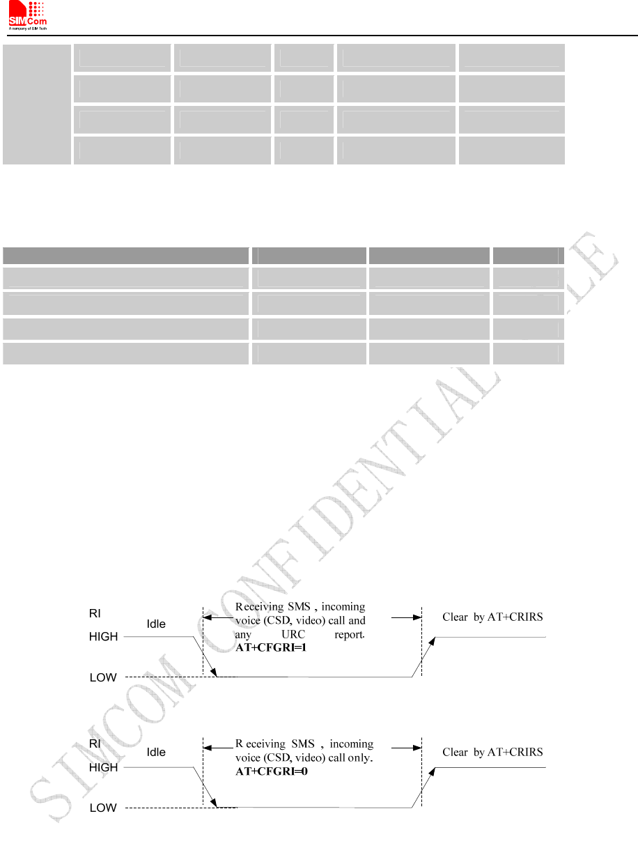
If UART port is used in Null Modem, the pin “RI” can be used as an interrupt signal to HOST. Normally it
will keep high logic level until certain condition such as receiving SMS, voice call (CSD, video) or URC
reporting, then “RI” will change to low logic level to inform the master (client PC). It will stay low until
the master clears the interrupt event with AT command.
Figure 20: RI behaviour in NULL Modem
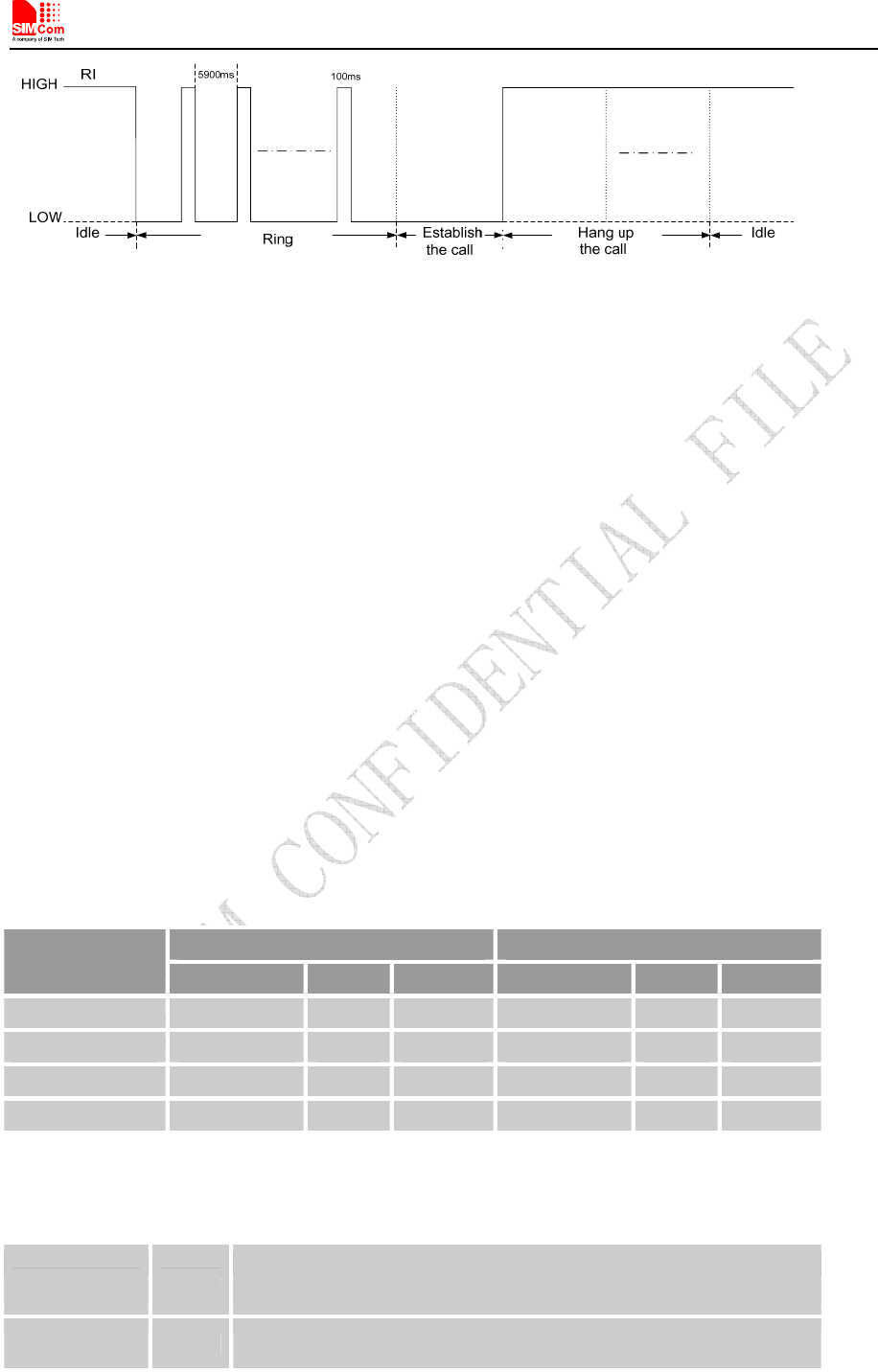
If Full Modem is used to establish communication between devices, the pin “RI” is another operation
status. Initially it keeps high, when a voice call or CSD call comes, the pin “RI” will change to low for
about 5900ms, then it will return to high level for 100ms. It will repeat this procedure until this call is
answered or hung up.
Smart Machine Smart Decision
SIM5320_Hardware Design_V1.01 2011-11-10
29
Figure 21: RI behaviour in FULL Modem
To comply with RS-232 protocol, the RS-232 level shifter chip should be used to connect SIM5320AD to
the RS-232-C interface. In this connection, the TTL level and RS-232 level are converted mutually.
SIMCom recommends that user uses the SP3238ECA chip with a full modem. For more information
please refers to the RS-232 chip datasheet.
Note: SIM5320AD supports the communication rate: 300, 600, 1200, 2400, 4800, 9600, 19200, 38400, 57600, 115200,
230400, 460800, 921600, 3200000, 3686400, 4000000bps. Default rate is 115200bps.
3.4 USIM Interface
The USIM provides the required subscription verification information to allow the mobile equipment to
attach to a GSM or UMTS network. Both 1.8V and 3.0V SIM Cards are supported.
3.4.1 Pin description
Table 9: Electronic characteristic
Table 10: Pin description
3.0V mode 1.8V mode
Pin name Min Typ Max Min Typ Max
V_USIM 2.7 3.00 3.3 1.65 1.8 2.0
USIM_RESET 0.8* V_USIM 3.00 V_USIM 0.8* V_USIM 1.8 V_USIM
USIM_CLK 0.7* V_USIM 3.00 V_USIM 0.8* V_USIM 1.8 V_USIM
USIM_DATA 0.7* V_USIM 3.00 V_USIM 0.8* V_USIM 1.8 V_USIM
Pin name Pin Description
USIM_CLK 19 USIM Card Clock
USIM_RESET 18 USIM Card Reset
USIM_DATA 17
USIM Card data I/O, which has been pulled up with a 22kR resistor to
V_USIM in module. Do not pull up or pull down in users’ application
circuit.
V_USIM 20 USIM Card Power output depends automatically on USIM mode,one
is 3.0V±10%, another is 1.8V±10%. Current is less than 50mA.
Smart Machine Smart Decision
SIM5320_Hardware Design_V1.01 2011-11-10
30
3.4.2 Application Guide
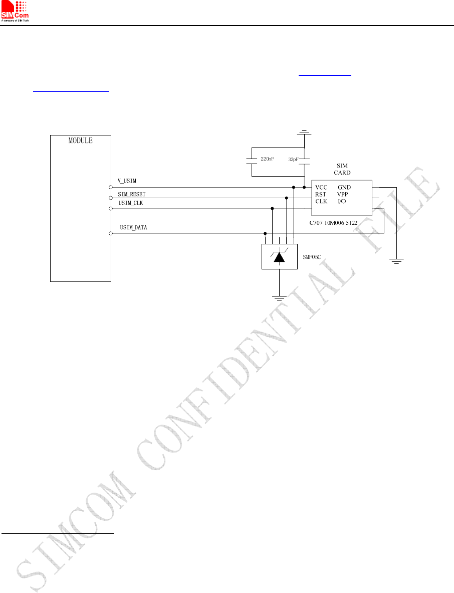
It is recommended to use an ESD protection component such as ST (www.st.com ) ESDA6V1W5 or ON
SEMI (www.onsemi.com ) SMF05C. Note that the SIM peripheral circuit should be close to the SIM card
socket. The reference circuit of the 8-pin SIM card holder is illustrated in the following figure.
Figure 22: USIM interface reference circuit
Note: USIM_DATA has been pulled up with a 22kR resistor to V_USIM in module. A 220nF shut capacitor on V_USIM
is used to reduce interference. Use AT Commands to get information in USIM card. For more detail, please refer to
document [1].
3.4.3 Recommend Components
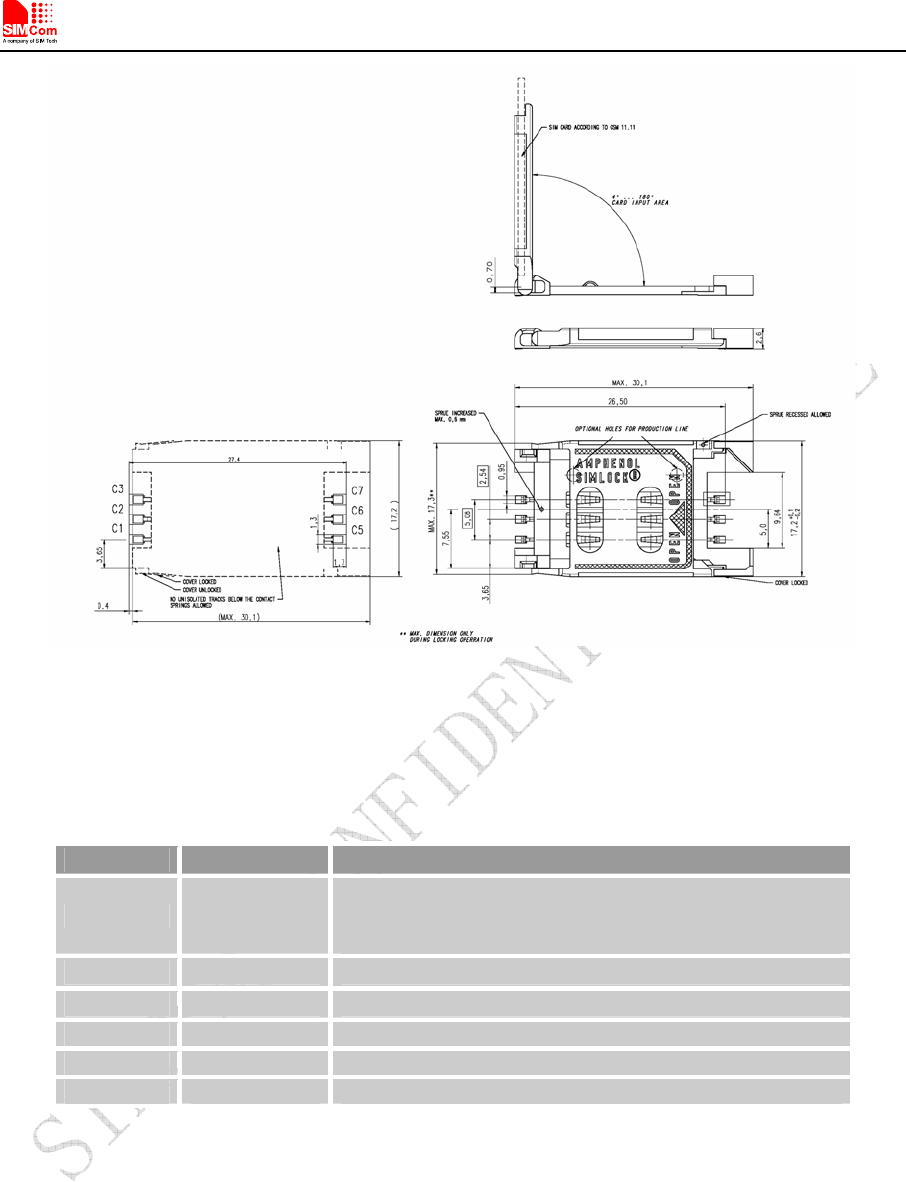
For 6 pins USIM socket, SIMCom recommend to use Amphenol C707 10M006 512 2. User can visit
http://www.amphenol.com for more information about the holder.
Smart Machine Smart Decision
SIM5320_Hardware Design_V1.01 2011-11-10
31
Figure 23: Amphenol SIM card socket
Table 11:: Amphenol USIM socket pin description
Pin Signal Description
C1 USIM_VDD
SIM Card Power supply, it can identify automatically the
SIM Card power mode,one is 3.0V±10%, another is
1.8V±10%.
C2 USIM_RST SIM Card Reset.
C3 USIM_CLK SIM Card Clock.
C5 GND Connect to GND.
C6 VPP Connect to USIM_VDD
C7 USIM_DATA SIM Card data I/O.
3.5 I2C Interface
I2C is used to communicate with peripheral equipments and can be operated as either a transmitter or
receiver, depending on the device function. Use AT Commands “AT+CRIIC and AT+CWIIC” to read/write
register values of related peripheral equipments connected with I2C interface.

Smart Machine Smart Decision
SIM5320_Hardware Design_V1.01 2011-11-10
32
3.5.1 Pin Description
Table 12: Pin description
3.5.2 Signal Description
Both SDA and SCL are bidirectional lines, connected to a positive supply via a pull-up resistor
respectively. When the bus is free, both lines are high.
3.5.3 Design Guide
For SIM5320AD, the data on the I2C bus can be transferred at rates up to 400kbps. The number of
peripheral devices connected to the bus is solely dependent on the bus capacitance limit of 400pF. Note
that PCB traces length and bending are in users’ control to minimize load capacitance.
Note
:
I2C_SDA and I2C _SCL have been pulled up with two 2.2kR resistors to 2.6V level in module. So there is no need
to pull them up in users’ application circuit.
3.6 USB Interface
SIM5320AD module contains a USB interface. This interface is compliant with the USB2.0 specification.
The USB2.0 specification requires hosts such as the computer to support all three USB speeds, namely
low-speed (1.5Mbps), full-speed (12Mbps) and high-speed (480Mbps). USB charging and USB-OTG is
not supported.
Table 13: Electronic characteristic
Input voltage scope( V )
Pin name Pin No. Min Typ Max
USB_VBUS 11 4.4 5.0 5.25
USB_DP 13
USB_DM 12
They are compliant with the USB 2.0 specification.
Pin name Pin No. Function
I2C_SDA 56 Serial interface data input and output
I2C_SCL 55 Serial interface clock input
Smart Machine Smart Decision
SIM5320_Hardware Design_V1.01 2011-11-10
33
3.6.1 Application Guide
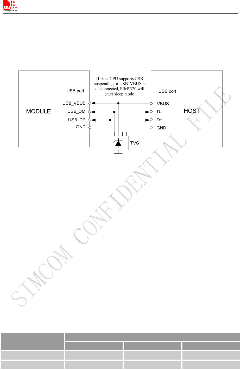
Currently SIM5320AD supports the USB suspend and resume mechanism which can help to save power.
If no transaction is on USB bus, SIM5320AD will enter suspend mode. When some events such as voice
call or receiving SMS happen, SIM5320AD will resume normal mode automatically.
Figure 24: USB interface
Because of high bit rate on USB bus, pay attention to influence of junction capacitance of ESD component
on USB data lines. Typically, the capacitance should be less than 4pF @1MHz.
Note
:
The SIM5320AD has two kinds of interface (UART and USB) to connect to host CPU. USB interface is mapped
to five virtual ports: “SIMTECH USB Modem”, “SIMTECH NMEA Device”, “SIMTECH ATCOM Device”,
“SIMTECH Diagnostics interface” and “SIMTECH Wireless Ethernet Adapter”.
3.7 SPI Interface
SPI interface of SIM5320AD is master only. It provides a duplex, synchronous, serial communication link
with peripheral devices. Its operation voltage is 1.8V, with clock rates up to 26 MHz.
3.7.1 Pin Description
Table 14: Electronic characteristic
1.8V mode
Pin name Min Typ Max
SPI_CLK 1.65 1.8 1.95
SPI_CS_N 1.65 1.8 1.95

Smart Machine Smart Decision
SIM5320_Hardware Design_V1.01 2011-11-10
34
SPI_MOMI_DATA 1.65 1.8 1.95
SPI_MIMO_DATA 1.65 1.8 1.95
Table 15: Pin description
3.8 GPIO Interface
SIM5320AD provides a limited number of GPIO pins. All GPIOs can be configured as inputs or outputs.
User can use AT Commands to read or write GPIOs status. Refer to ATC document for details.
3.8.1 Pin Description
Table 16: Electronic characteristic
Note: If more GPIOs need to be used, users can configure GPIO on other multiple function interfaces,. Please refer to
GPIO list.
Pin name Pin No. Function
SPI_CS 9 SPI chip-select; not mandatory in a point-to-point connection
SPI_MISO_DATA 7 SPI master in/slave out data
SPI_CLK 6 SPI clock
SPI_MOSI_DATA 8 SPI master out/slave in data
2.6V mode
Pin name Min Typ Max
GPIO1 2.5 2.6 2.7
GPIO4 2.5 2.6 2.7
GPIO40 2.5 2.6 2.7
GPIO41 2.5 2.6 2.7
GPIO43 2.5 2.6 2.7
GPIO44 2.5 2.6 2.7
GPIO42 2.5 2.6 2.7
Smart Machine Smart Decision
SIM5320_Hardware Design_V1.01 2011-11-10
35
Table 17: Pin description
Note: The output driver current of GPIOs is 1mA at the lower supply voltage and 2mA at the higher supply voltage.
3.8.2 Application Guide
Network status
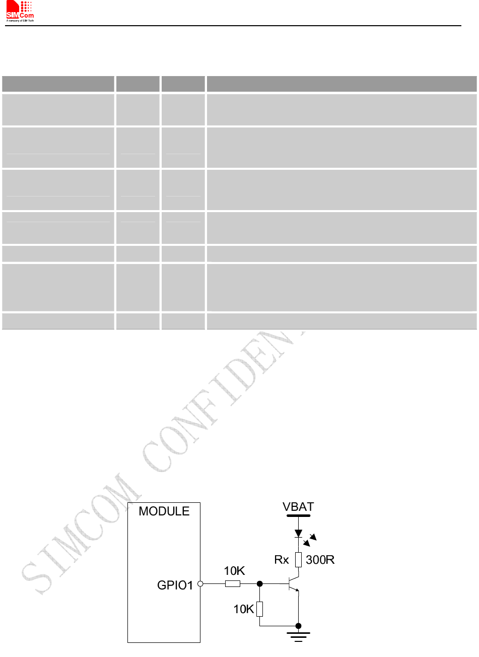
GPIO1 is used to control Network Status LED; application circuit is shown below.
Figure 25: Application circuit
Note: The value of resistor Rx depends on LED characteristic.
Pin name Pin No. I/O Function
GPIO1 51 O Output PIN as LED control for network status. If it is
unused, left open.
GPIO4 54 I
Input PIN as RF operating control.
H: Normal Mode L:Flight Mode
If it is unused, left open.
GPIO40 49 O
Output PIN as operating status indicating of module.
H: Power on L: Power off
If it is unused, left open.
GPIO41 52 I/O General input/output PIN. It can be used as wake/interrupt
signal to host from module If it is unused, left open.
GPIO42 53 I/O General Purpose Input/Output Port.
GPIO43 50 I/O
General Purpose Input/Output Port. It can be used as
wake/interrupt signal to module from host. If it is unused, left
open.
GPIO44 48 I/O General Purpose Input/Output Port
Smart Machine Smart Decision
SIM5320_Hardware Design_V1.01 2011-11-10
36
Table 18: LED status
LED Status Module Status
Always On Searching Network/Call Connect
200ms ON, 200ms OFF Data Transmit
800ms ON, 800ms OFF Registered network
Off Power off / Sleep
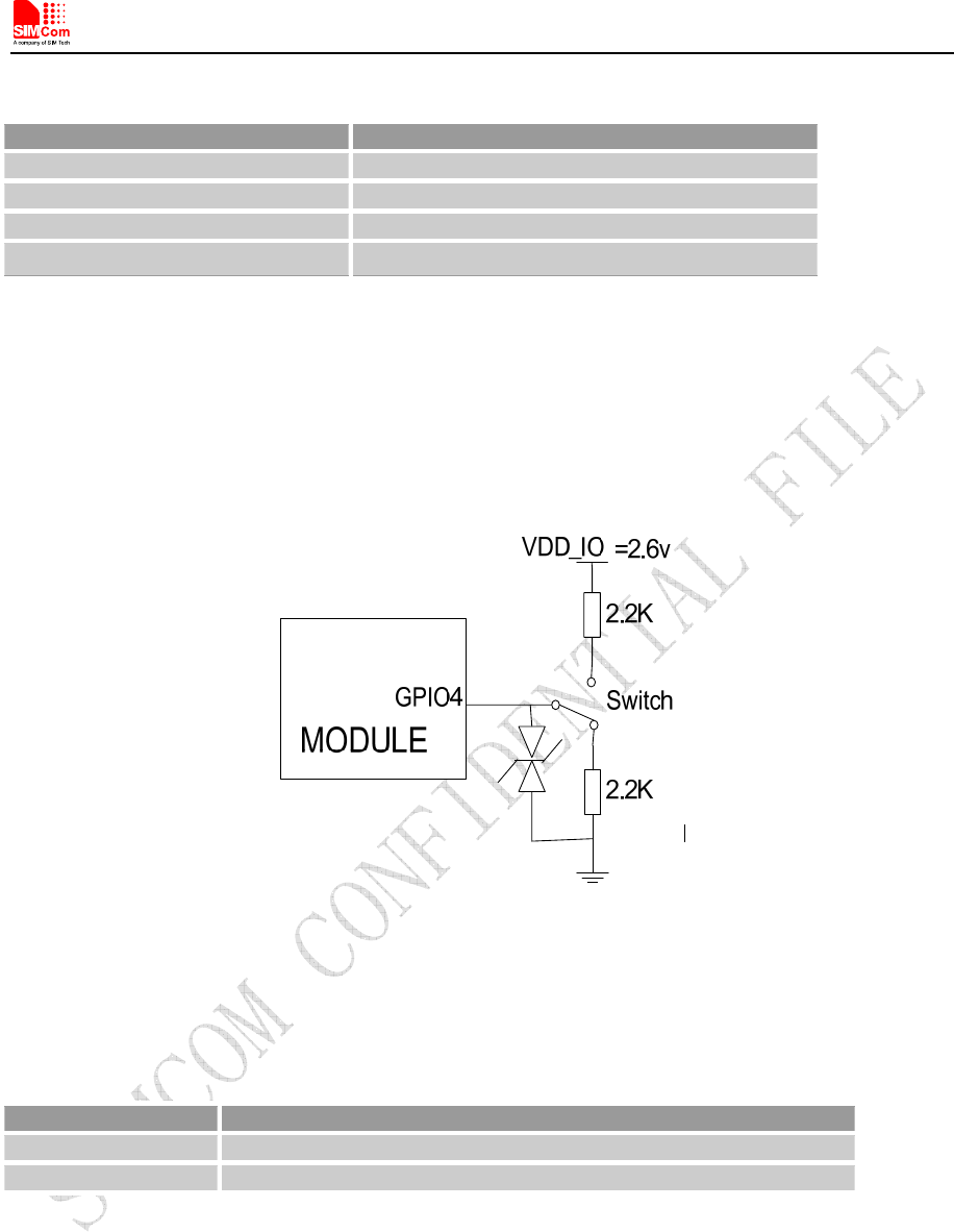
Flight mode control
GPIO4 controls SIM5320AD module to enter or exit the Flight mode. In Flight mode, SIM5320AD closes
RF function to prevent interference with other equipments or minimize current consumption. Bidirectional
ESD protection component is suggested to add on GPIO4.
Figure 26: Flight mode switch
Table 19: Control status
GPIO4 Status Module operation
Low Level Flight Mode: RF is closed.
High Level Normal Mode: RF is working.
Note
:
1. When the module is powered off, make sure all digital interfaces (UART, etc) connected with peripheral devices have
no voltage higher than 0.3V. If users’ design cannot meet above conditions, high level voltages maybe occur in GPIO pins
because current leakage from above digital interfaces may occur.

Smart Machine Smart Decision
SIM5320_Hardware Design_V1.01 2011-11-10
37
3.9 Global Positioning System
SIM5320AD merges GPS satellite and network information to provide a high-availability solution that
offers industry-leading accuracy and performance. This solution performs well, even in very challenging
environmental conditions where conventional GPS receivers fail, and provides a platform to enable
wireless operators to address both location-based services and emergency mandates.
3.9.1 Technical specification
Tracking sensitivity -157 dBm
Cold-start sensitivity -144 dBm
Accuracy (Open Sky) <2m (CEP50)
TTFF (Open Sky) Hot start <1s Cold start 35s(good signal)/ 100s(weak signal)
Receiver Type 12-channel, GPS L1 Frequency (1575.42MHz), C/A Code
Update rate Default 1 Hz
GPS data format NMEA-0183
GPS Current consumption (WCDMA/GSM Sleep mode) 100mA (Total supply current)
GPS antenna Passive/Active antenna
Note: Performance will vary depending on the environment, antenna type and signal conditions and so on.
3.9.2 Operate Mode
SIM5320AD supports both A-GPS and S-GPS, and then provides three operating modes: mobile-assisted
mode, mobile-based mode and standalone mode. A-GPS includes mobile-assisted and mobile-based mode.
In mobile-assisted mode, when a request for position location is issued, available network information is
provided to the location server (e.g. Cell-ID) and assistance is requested from the location server. The
location server sends the assistance information to the handset. The handset/mobile unit measures the GPS
observables and provides the GPS measurements along with available network data (that is appropriate for
the given air interface technology) to the location server. The location server then calculates the position
location and returns results to the requesting entity.
In mobile-based mode, the assistant data provided by the location server encompasses not only the
information required to assist the handset in measuring the satellite signals, but also the information
required to calculate the handset’s position. Therefore, rather than provide the GPS measurements and
available network data back to the location server, the mobile calculates the location on the handset and
passes the result to the requesting entity.
In standalone (autonomous) mode, the handset demodulates the data directly from the GPS satellites.
This mode has some reduced cold-start sensitivity, and a longer time to first fix as compared to the assisted
modes. However, it requires no server interaction and works out of network coverage.
This combination of GPS measurements and available network information provides:
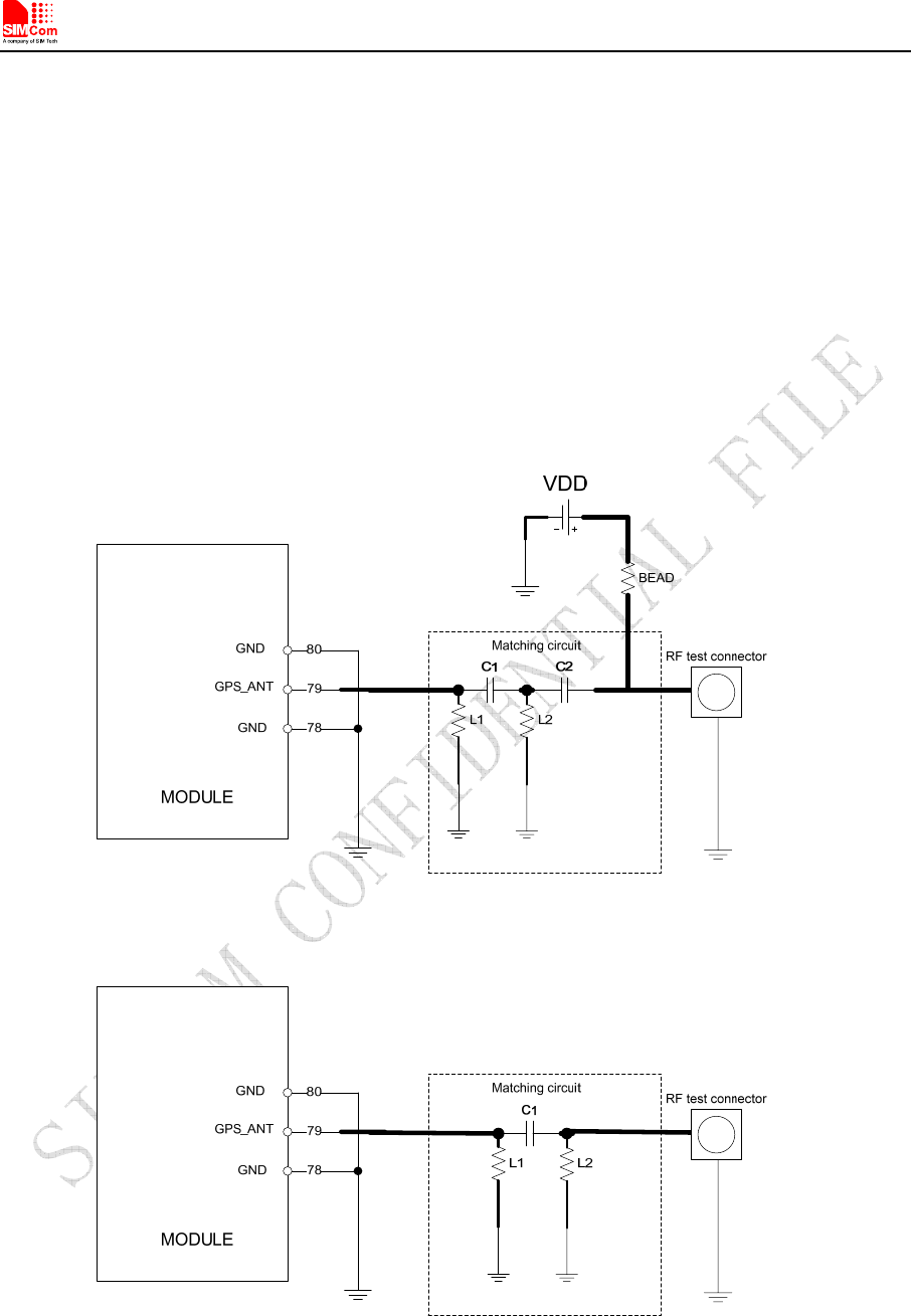
Smart Machine Smart Decision
SIM5320_Hardware Design_V1.01 2011-11-10
38
● High-sensitivity solution that works in all terrains: Indoor, outdoor, urban, and rural
● High availability that is enabled by using both satellite and network information
Therefore, while network solutions typically perform poorly in rural areas and areas of poor cell
geometry/density, and while unassisted, GPS-only solutions typically perform poorly indoors. The
SIM5320AD GPS solution provides optimal time to fix, accuracy, sensitivity, availability, and reduced
network utilization in both of these environments, depending on the given condition.
3.9.3 Application Guide
Users can adopt an active antenna or a passive antenna as GPS signal transceiver. In this document, all
GPS specification mentioned is from passive antenna. The following is the reference circuit.
Figure 27: Active antenna circuit
Figure 28:Passive antenna circuit (Default)
In above figures, the components C1 and L1, L2 are used for antenna matching, the values of the

Smart Machine Smart Decision
SIM5320_Hardware Design_V1.01 2011-11-10
39
components can only be obtained after the antenna tuning usually, and they are provided by antenna
vendor.C2 in Figure 27 is used for DC isolation. In active antenna circuit, users must use an external
LDO/DCDC to provide VDD voltage whose value should be taken according active antenna characteristic,
and VDD can be shut down to avoid consuming additional current when not being used.
GPS can be used by NMEA port. User can select NMEA as output through UART or USB. NMEA
sentences are automatic and no command is provided. NMEA sentences include GSV, GGA, RMC, GSA,
and VTG. Before using GPS, user should configure SIM5320AD in proper operating mode by AT
command. Please refer to related document for details. SIM5320AD can also get position location
information through AT directly.
Note:GPS is closed by default, it could be started by AT+CGPS. The AT command has two parameters, the first is on/off,
and the second is GPS mode. Default mode is standalone mode.
AGPS mode needs more support from the mobile telecommunication network. Refer to AGPS application document for
details.
3.10 Multi-functional interface
SIM5320AD merges functions for various applications. It can enrich users’ design and lower the cost of
users’ hardware.
3.10.1 Sink Current Source
The dedicated pin (CURRENT_SINK) is intended for driving passive devices,such as LCD backlight, this
implementation is +5V tolerant and suitable for driving white LEDs. The high-current driver can maintain
a constant current which is set by the AT command “AT+ CLEDITST”, capable of up to 150 mA.
Table 20: Electronic characteristic
Symbol Description Min Typ Max Unit
CURRENT_SINK Input voltage 0.5 VDD 5 V
IO Input current - - 150 mA
Since the driver is ground-referenced current sink, the operating device it drives must form a current path
between the VDD pin and the CURRENT_SINK pin. The following figure is for users reference.
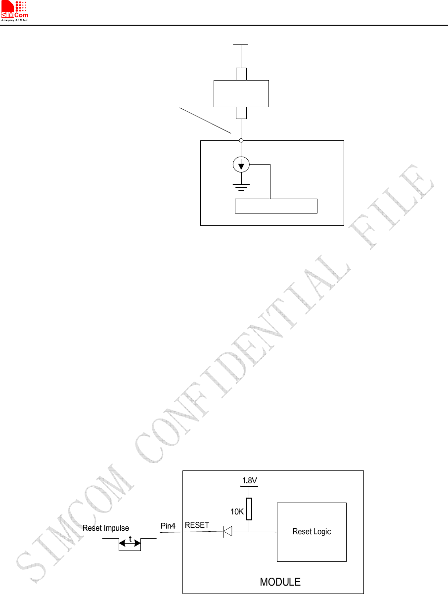
Smart Machine Smart Decision
SIM5320_Hardware Design_V1.01 2011-11-10
40
MODULE
CURRENT_SINK
Pin 45 is +5V tolerant-
suitable for driving white
LEDs
Current Controls
Passive
device
+
-
VBAT
High
current
Figure 29: Current drive
Note: The sinking current can be adjusted to meet design requirement through the AT command “AT+ CLEDITST =<0>,
<value>”.The “value” ranges from 0 to 15,on behalf of the current changes from 0mA to 150mA in steps of 10mA.
3.10.2 Reset Function
SIM5320AD also have a RESET pin (PIN4) to reset the module. This function is used as an emergency
reset only when AT command “AT+CPOF” and the POWER_ON pin has no effect. User can pull the
RESET pin to ground, then the module will reset.
This pin is already pulled up in module, so the external pull-up resistor is not necessary. A 100nF capacitor
close to the RESET pin is strongly recommended. A reference circuit is recommended in the following
figure.
Figure 30: Reset circuit
Note
:
50ms<t<200ms. ESD components are suggested to be used on Reset pin.
3.10.3 ADC
SIM5320AD has a dedicated ADC that is available for digitizing analog signals such as battery voltage
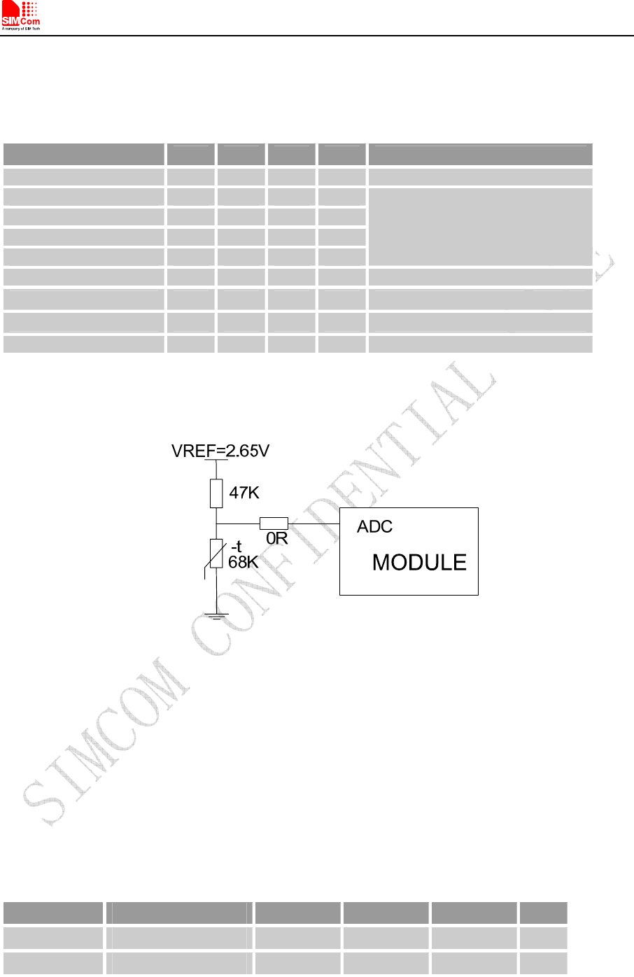
Smart Machine Smart Decision
SIM5320_Hardware Design_V1.01 2011-11-10
41
and so on; it is on PIN 47 and PIN 46 , namely ADC1 and ADC2 . This ADC is 12 bit
successive-approximation circuit, and electronic specification is shown in the following table.
Table 21: Electronic Characteristics
Specification Min Typ Max Unit Comments/Conditions
Resolution 12 Bits
Differential nonlinearity -4 +4 LSB
Integral nonlinearity -8 +8 LSB
Gain Error -2.5 +2.5 %
Offset Error -4 +40 LSB
Analog Vdd = ADC reference
2.4MHz sample rate
Input Range GND 2.2V V
Input serial resistance 2 kΩ Sample and hold switch resistance
Input capacitance 53 pF
Power-down to wakeup 9.6 19.2 μs
User can introduce a signal in the ADC pin directly and use the AT command “AT+CADC” to get the raw
data which is between 0 and 255. The data can be transformed to any type such as voltage, temperature etc.
Please refer to Chapter 3.1.2 and document [1].
Figure 31: Reference circuit
Note: The input signal voltage value in ADC must not be higher than 2.2V.
3.10.4 LDO
SIM5320AD has a LDO power output, namely VREG_AUX. The LDO is available and output voltage is
2.85v by default, rated for 250mA. User can switch the LDO on or off by the AT command
“AT+CVAUXS” and configure its output voltage by the AT command “AT+CVAUXV”.
Table 22: Electronic characteristic
Symbol Description Min Typ Max Unit
VREG_AUX Output voltage 1.5 2.85 3.05 V
IO Output current - - 250 mA
Smart Machine Smart Decision
SIM5320_Hardware Design_V1.01 2011-11-10
42
4 RF Specification
4.1 RF Specification
Table 23: Conducted transmission power
Frequency Max Min
GSM850 33dBm ±2dB 5dBm ± 5dB
E-GSM900 33dBm ±2dB 5dBm ± 5dB
DCS1800 30dBm ±2dB 0dBm ± 5dB
PCS1900 30dBm ±2dB 0dBm ± 5dB
GSM850 (8-PSK) 27dBm ±3dB 5dBm ± 5dB
E-GSM900 (8-PSK) 27dBm ±3dB 5dBm ± 5dB
DCS1800 (8-PSK) 26dBm +3/-4dB 0dBm ±5dB
PCS1900(8-PSK) 26dBm +3/-4dB 0dBm ±5dB
WCDMA 1900 24dBm +1/-3dB -56dBm ±5dB
WCDMA 850 24dBm +1/-3dB -56dBm ±5dB
Table 24: Operating frequencies
Frequency Receiving Transmission
GSM850 869 ~894 MHz 824 ~849 MHz
E-GSM900 925 ~960 MHz 880 ~915 MHz
DCS1800 1805~1880 MHz 1710~1785 MHz
PCS1900 1930~1990 MHz 1850~1910 MHz
WCDMA1900 1930~1990 MHz 1850~1910 MHz
WCDMA 850 869 ~894 MHz 824 ~849 MHz
Table 25: Conducted receive sensitivity
Frequency Receive sensitivity
GSM850 < -106dBm
E-GSM900 < -106dBm
DCS1800 < -106dBm
DCS1800 < -106dBm
WCDMA 1900 < -108dBm
WCDMA 850 < -106dBm
Smart Machine Smart Decision
SIM5320_Hardware Design_V1.01 2011-11-10
43
4.2 Operating Specification
SIM5320AD can support high rate data by GSM/WCDMA wireless network. In the different network
environment, data transmission rate shifts depending on modulation and encoding.
Table 26: GPRS/EDGE data throughout
Function Coding schemes 1 Timeslot 2 Timeslot 4 Timeslot
CS-1 9.05kbps 18.1kbps 36.2kbps
CS-2 13.4kbps 26.8kbps 53.6kbps
CS-3 15.6kbps 31.2kbps 62.4kbps
GPRS
CS-4 21.4kbps 42.8kbps 85.6kbps
MCS-1 8.80kbps 17.6kbps 35.20kbps
MCS-2 11.2kbps 22.4kbps 44.8kbps
MCS-3 14.8kbps 29.6kbps 59.2kbps
MCS-4 17.6kbps 35.2kbps 70.4kbps
MCS-5 22.4kbps 44.8kbps 89.6kbps
MCS-6 29.6kbps 59.2kbps 118.4kbps
MCS-7 44.8kbps 89.6kbps 179.2kbps
MCS-8 54.4kbps 108.8kbps 217.6kbps
EDGE
MCS-9 59.2kbps 118.4kbps 236.8kbps
Table 27: HSDPA throughout
Category Supported Max supported
HS-DSCH codes
Theoretical max
peak rate(Mbps) Modulation
Category1 5 1.2 16QAM,QPSK
Category2 5 1.2 16QAM,QPSK
Category3 5 1.8 16QAM,QPSK
Category4 5 1.8 16QAM,QPSK
Category5 3 5 3.6 16QAM,QPSK
Category6 3 5 3.6 16QAM,QPSK
Category7 10 7.2 16QAM,QPSK
Category8 10 7.2 16QAM,QPSK
Category9 15 10.0 16QAM,QPSK
Category10 15 14.0 16QAM,QPSK
Category11 5 0.9 QPSK
Category12 3 5 1.8 QPSK
Note: Actual throughout rates depend on network configuration, network loading, signal condition and so on.
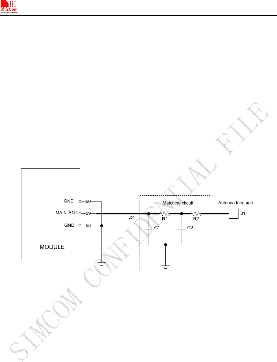
Smart Machine Smart Decision
SIM5320_Hardware Design_V1.01 2011-11-10
44
4.3 Antenna Design Guide
SIM5320AD provides RF antenna interface. Customer’s antenna should be located in the host board and
connected to module’s antenna pad through micro-strip line or other types of RF trace and the trace
impedance must be controlled in 50Ω. SIMCom recommends that the total insertion loss between the
antenna pad and antenna should meet the following requirements:
● GSM900/GSM850<0.5dB
● DCS1800/PCS1900 <0.9dB
● WCDMA 1900<0.9dB
● WCDMA 850<0.5dB
To facilitate the antenna tuning and certification test, a RF connector and an antenna matching circuit
should be added. The following figure is the recommended circuit.
Figure 32: Antenna matching circuit
In this figure, the components R1,C1,C2 and R2 is used for antenna matching, the value of components
can only be got after the antenna tuning, usually, they are provided by antenna vendor. By default, the R1,
R2 are 0 ohm resistors, and the C1, C2 are reserved for tuning.
The RF test connector in the figure is used for the conducted RF performance test, and should be placed as
close as to the module’s antenna pin. The traces impedance between components must be controlled in
50ohm.
Smart Machine Smart Decision
SIM5320_Hardware Design_V1.01 2011-11-10
45
5 Reliability and Operating Characteristics
5.1 Electronic Characteristics
Absolute maximum rating for digital and analog pins of SIM5320AD are listed in the following table:
Table 28: Absolute maximum ratings
Parameter Min Max Unit
Voltage at digital pins (1.8v mode) -0.3 1.8+0.3 V
Voltage at digital pins (2.6v mode) -0.3 2.6+0.3 V
Voltage at VBAT -0.5 6.0 V
Voltage at VRTC 1.5 3.2 V
Voltage at USB_VBUS -0.5 6.0 V
Table 29: Recommended operating ratings
Parameter Min Typ Max Unit
Voltage at digital pins (1.8v mode) 1.65 1.8 1.95 V
Voltage at digital pins (2.6v mode) 2.5 2.6 2.7 V
Voltage at VBAT 3.3 3.8 4.2 V
Voltage at VRTC 1.5 - 3.0 V
Voltage at USB_VBUS 4.75 5 5.25 V
The operating temperature and power specification is listed in the following table.
Table 30: Operating temperature
Parameter Min Typ Max Unit
Ambient temperature -30 25 80 ℃
Storage temperature -40 25 +85 ℃
Note: SIMCom recommends user to install a heat sink on the module shielding case if SIM5320AD operates in WCDMA
band.
5.2 Operating Mode
The following table summarizes the various operating modes, each operating modes will be referred to in
the following chapters.

Smart Machine Smart Decision
SIM5320_Hardware Design_V1.01 2011-11-10
46
5.2.1 Operating Modes Overview
Table 31: Operating Modes Overview
Mode Function
Sleep mode GSM/WCDM
A SLEEP
Module will automatically enter SLEEP mode if DTR is set to high
level and there is no on air or hardware interrupt (such as GPIO
interrupt or data on serial port).
In this case, the current consumption of module will be reduced to the
minimal level.
In SLEEP mode, the module can still receive paging message,voice
call and SMS.
GSM GSM IDLE Software is active. Module has registered to the GSM network, and
the module is ready to communicate.
GPRS
STANDBY
Module is ready for GPRS data transfer, but no data is currently sent
or received. In this case, power consumption depends on network
settings and GPRS configuration.
GPRS
GPRS DATA
There is GPRS data transfer (PPP or TCP or UDP) in progress. In this
case, power consumption is related with network settings (e.g. power
control level), uplink/downlink data rates and GPRS configuration
(e.g. used multi-slot settings).
EDGE
STANDBY
Module is ready for data transfer in EDGE mode, but no data is
currently sent or received. In this case, power consumption depends
on network settings and EDGE configuration
EDGE
EDGE DATA
There is EDGE data transfer (PPP or TCP or UDP) in progress. In this
case, power consumption is related with network settings (e.g. power
control level), uplink/downlink data rates and EDGE configuration.
WCDMA WCDMA
IDLE
Module has registered to the WCDMA network, and the module is
ready to communicate.
HSDPA IDLE
Module is ready for data transmission, but no data is currently sent or
received. Power consumption depends on network settings and
HSDPA configuration
HSDPA
HSDPA
DATA
There is HSDPA data transfer (PPP or TCP or UDP) in progress. In
this case, power consumption is related with network settings (e.g.
power control level), uplink/downlink data rates and HSDPA
configuration
Power down
Module can be powered down by the AT command “AT+CPOF” or the POWER_ON
pin. The power management unit shuts down the power supply of the module, only the
power supply of RTC is remained. The serial interface is not accessible. Operating
voltage (connected to VBAT) remains applied.
Minimum
functionality
mode
The AT command “AT+CFUN” can be used to set the module to a minimum
functionality mode without removing the power supply. In this mode, the RF part of
the module will not work or the SIM card will not be accessible, or both will be closed,
and the serial port is still accessible. The power consumption in this mode is very low.
5.2.2 Minimize Power Consumption
There are two modes that SIM5320AD achieves low power consumption.

Smart Machine Smart Decision
SIM5320_Hardware Design_V1.01 2011-11-10
47
Sleep mode
If peripheral equipments stops working, and there is no on air or hardware interrupts (such as GPIO
interrupts or data on UART), SIM5320AD will enter sleep mode automatically. In this mode, SIM5320AD
can still receive paging,voice call or SMS from network. If USB interface of SIM5320AD is connected to
host CPU, but host CPU does not support USB suspending, then SIM5320AD will not enter sleep mode.
After USB is disconnected, SIM5320AD will enter sleep mode.
Note: When UART interface is connected with host CPU, SIM5320AD can not enter sleep mode until RXD is pulled
down by the host CPU. If the module is in the idle mode, make sure to pull the RXD to low level by host CPU. SIMCom
recommends using GPIO43 or UART_DTR to wake up the module from host CPU and to use GPIO41 or UART_RI to
wake up the host CPU. Before designing, pay attention to how to realize waking function and refer to Document[24] and
Document[25] for more detail.
Minimum functionality mode
Minimum functionality mode ceases a majority function of module, thus minimizing the power
consumption. This mode is set by the AT command which provides a choice of the functionality levels.
● AT+CFUN=0: Minimum functionality
● AT+CFUN=1: Full functionality (Default)
● AT+CFUN=4: Disable RF function of the module (Flight mode)
If SIM5320AD has been set to minimum functionality mode, the module will firstly enter sleep mode,
then the RF function and SIM card function will be closed. In this case, the serial port is still accessible,
but RF function or SIM card will be unavailable. When SIM5320AD is in minimum functionality or flight
mode, it can return to full functionality by the AT command “AT+CFUN=1”.
Note: For flight mode, please refer to Chapter3.9.2.
5.3 Current Consumption
The current consumption in suspended mode and without USB connection is listed in the table below.
Here, “suspended mode” means that SIM5320AD is connected to USB bus, but it does not transfer data.
Table 32: Current consumption
GSM Sleep mode (without USB connection)
GSM850
Sleep @DRX=2 4.5mA
Sleep @DRX=5 2.7mA
Sleep @DRX=9 2.3mA
GSM900 Sleep @DRX=2 4.5mA

Smart Machine Smart Decision
SIM5320_Hardware Design_V1.01 2011-11-10
48
Sleep @DRX=5 2.7mA
Sleep @DRX=9 2.3mA
DCS1800
Sleep @DRX=2 4.5mA
Sleep @DRX=5 2.7mA
Sleep @DRX=9 2.3mA
PCS1900
Sleep @DRX=2 4.5mA
Sleep @DRX=5 2.7mA
Sleep @DRX=9 2.3mA
GSM Sleep Mode (with USB suspended)
GSM850
Sleep @DRX=2 4.6mA
Sleep @DRX=5 2.8mA
Sleep @DRX=9 2.5mA
GSM900
Sleep @DRX=2 4.6mA
Sleep @DRX=5 2.8mA
Sleep @DRX=9 2.5mA
DCS1800
Sleep @DRX=2 4.6mA
Sleep @DRX=5 2.8mA
Sleep @DRX=9 2.5mA
PCS1900
Sleep @DRX=2 4.6mA
Sleep @DRX=5 2.8mA
Sleep @DRX=9 2.5mA
DATA mode, GPRS ( 1 Rx,4 Tx ) CLASS 12
GSM 850 @power level #5 <660mA,Typical 488mA
GSM 900 @power level #5 <660mA,Typical 484mA
DCS1800 @power level #0 <530mA,Typical 346mA
PCS1900 @power level #0 <530mA,Typical 353mA
DATA mode, GPRS ( 3Rx, 2 Tx ) CLASS 12
GSM 850 @power level #5 <460mA,Typical 335mA
GSM 900 @power level #5 <440mA,Typical 332mA
DCS1800 @power level #0 <400mA,Typical 260mA
PCS1900 @power level #0 <300mA,Typical 263mA
EDGE Data
DATA mode, EDGE( 1 Rx,4 Tx ) CLASS 12
GSM 850 @power level #8 <500mA,Typical 335mA
GSM 900 @power level #8 <500mA,Typical 332mA
DCS1800 @power level #2 <450mA,Typical 291mA
PCS1900 @power level #2 <450mA,Typical 293mA
DATA mode, EDGE( 3Rx, 2 Tx ) CLASS 12
GSM 850 @power level #8 <330mA,Typical 235mA
GSM 900 @power level #8 <330mA,Typical 231mA
DCS1800 @power level #2 <300mA,Typical 206mA
PCS1900 @power level #2 <300mA,Typical 209mA
UMTS Sleep Mode (without USB connection)
WCDMA 1900 Sleep @DRX=9 2.2mA
Sleep @DRX=8 2.7 mA

Smart Machine Smart Decision
SIM5320_Hardware Design_V1.01 2011-11-10
49
Sleep @DRX=6 4.7mA
WCDMA 850
Sleep @DRX=9 2.2mA
Sleep @DRX=8 2.7 mA
Sleep @DRX=6 4.7mA
UMTS Sleep Mode (with USB suspended)
WCDMA 1900
Sleep @DRX=9 2.4mA
Sleep @DRX=8 2.8 mA
Sleep @DRX=6 4.8mA
WCDMA 850
Sleep @DRX=9 2.4mA
Sleep @DRX=8 2.8 mA
Sleep @DRX=6 4.8mA
HSDPA Data
WCDMA 1900
@Power 23dBm CQI=22 Typical 610mA
@Power 21dBm CQI=5 Typical 540mA
@Power -5dBm CQI=22 Typical 270mA
WCDMA 850
@Power 23dBm CQI=22 Typical 550mA
@Power 21dBm CQI=5 Typical 490mA
@Power -5dBm CQI=22 Typical 220mA
5.4 EMC and ESD Notes
EMC tests should be performed to detect any potential problems. Possible harmful emissions radiate by
the application to the RF receiver in the receiver band. It is recommended to shield the sensitive
components and trace with common ground and user can add beads where necessary.
Normally SIM5320AD is mounted on customer host board. Although some ESD components have been
added in SIM5320AD, to prevent ESD, user should put some ESD components on customers’ board. The
ESD components should be placed beside the connectors which human body might touch, such as SIM
card holder, switches, keys, etc. The following table is the SIM5320AD ESD measurement performance;
the results are from SIMCom EVB test.
Table 33: The ESD performance measurement table (Temperature: 25 , Humidity:℃ 45%)
Part Contact discharge Air discharge
VBAT,GND ±4KV ±6KV
UART,USB ±2KV ±6KV
Antenna port ±4KV ±6KV
Other ports ±2KV ±2KV
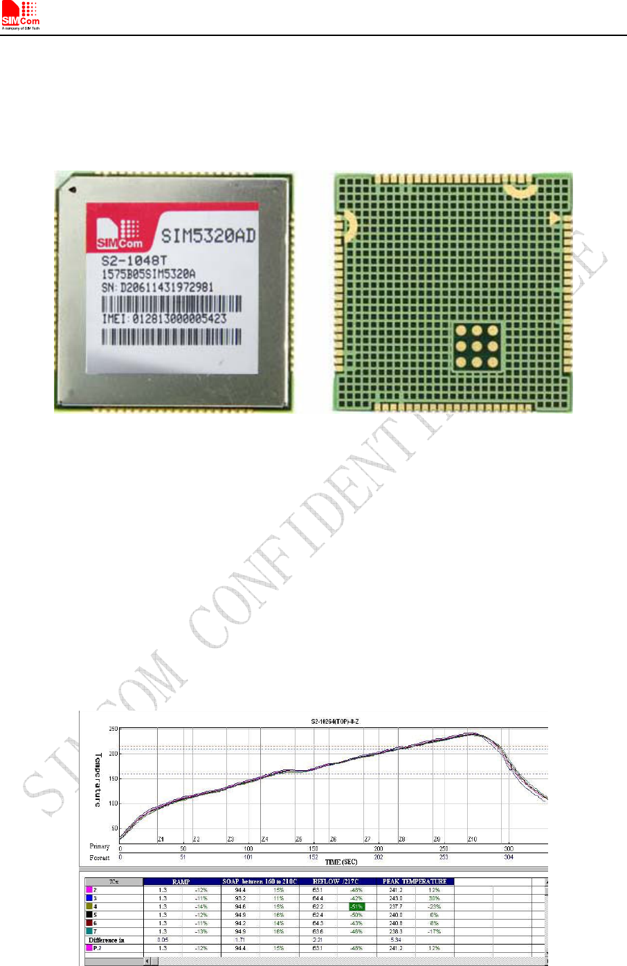
Smart Machine Smart Decision
SIM5320_Hardware Design_V1.01 2011-11-10
50
6 Guide for Production
6.1 Top and Bottom View of SIM5320AD
Figure 33: Top and bottom view of SIM5320AD
These test points are only used for module manufacturing and testing. They are not for customer’s
application.
6.2 Typical Solder Reflow Profile
For customer convenience, SIMCom provides a typical example for a commonly used soldering profile. In
final board assembly, the typical solder reflow profile will be determined by the largest component on the
board, as well as the type of solder/flux used and PCB stack-up. Therefore the soldering profile shown
below is only a generic recommendation and should be adjusted to the specific application and
manufacturing constraints.
Figure 34: The ramp-soak-spike reflow profile of SIM5320AD
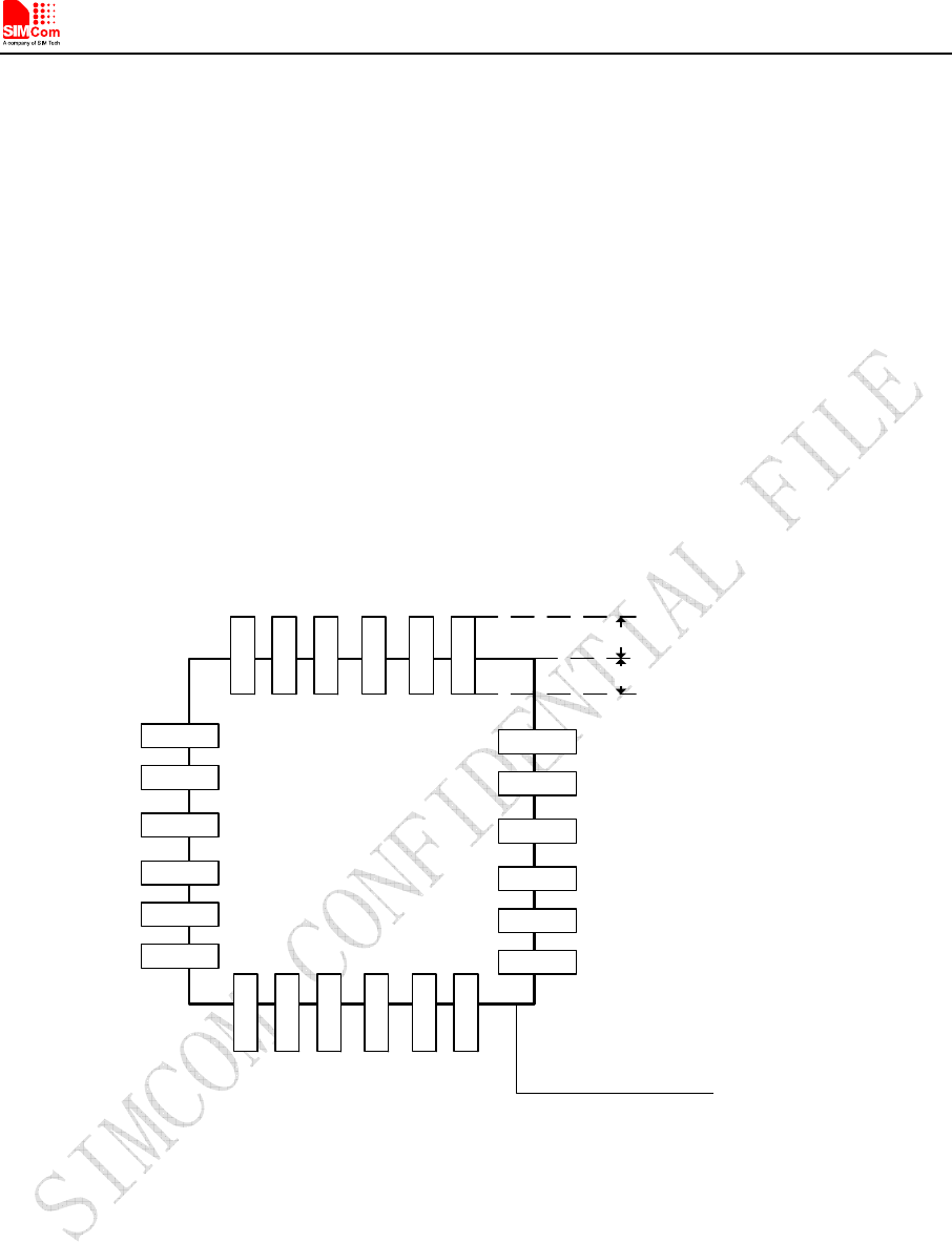
Smart Machine Smart Decision
SIM5320_Hardware Design_V1.01 2011-11-10
51
For details about secondary SMT, please refer to document [23].
6.3 Moisture Sensitivity Level (MSL)
SIM5320AD is qualified to Moisture Sensitivity Level (MSL) 5 in accordance with JEDEC J-STD-020.
After the prescribed time limit exceeded, users should bake modules for 192 hours in drying equipment
(<5% RH) at 40° C +5° C/-0° C, or 72 hours at 85° C +5° C/-5° C. Note that plastic tray is not
heat-resistant, users must not use the tray to bake at 85° C or the tray may be damaged.
6.4 Stencil Foil Design Recommendation
The recommended thickness of stencil foil is more than 0.15mm.
6.5 Recommended Pad Design
Module Outline
A
B
A:B=1.0mm:0.8mm
Figure 35: Recommended pad
Note: More designing details refer to Figure 6.
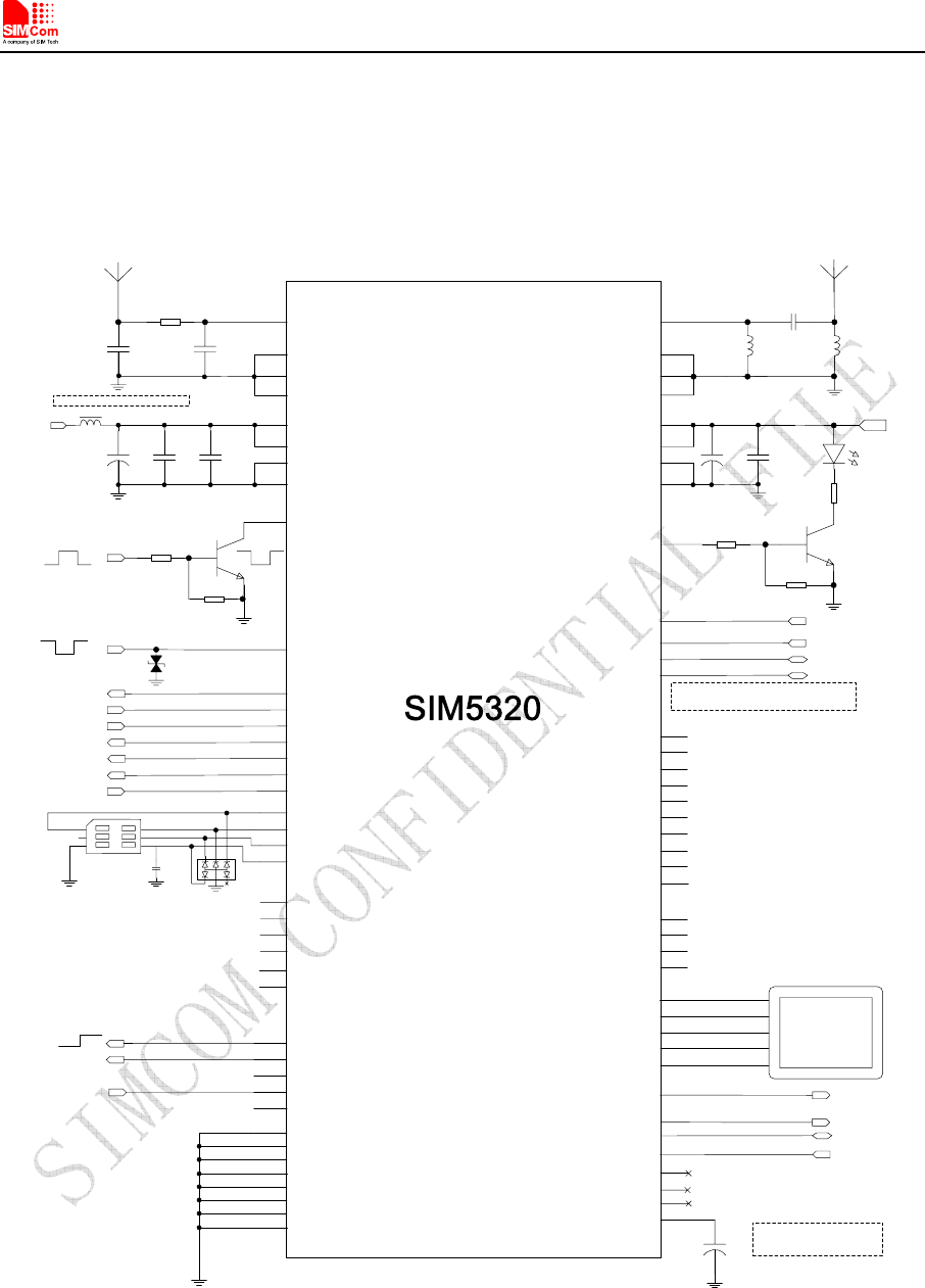
Smart Machine Smart Decision
SIM5320_Hardware Design_V1.01 2011-11-10
52
Appendix
A. System Design
C103C102C101
VBAT_RF
VBAT_RF
VBAT_BB
Power supply
100uF 100nF 22pF
UART_TXD
UART_RXD
UART_CTS
UART_RTS
UART_RI
UART_DCD
UART_DTR
C109
220nF
V_USIM
USIM_RESET
USIM_CLK
USIM_DATA
VBAT_BB
62
63
38
39
C105C104
100uF 100nF
Power supply
61
64
GND
GND
37
40
GND
GND
POWER_ON
RESET
3
4
Reset impulse
20~200ms
4.7K
47K
Turn on/off impulse
>50ms
UART_TXD
UART_RXD
UART_CTS
UART_RTS
UART_RI
UART_DCD
UART_DTR
71
68
67
66
69
70
72
23
1GND
GND
0R
C107C106
Main Antenna
NC NC
MAIN_ANT
59
58
GND
GND
57
C107
GPS Antenna
33pF
GPS_ANT 79
78
GND
GND
77 NC
L101 NC
L102
GND 80
GND
60
SIM_DATA
SIM_VDD
SIM_RST
SIM_CLK
SMF05C
NC
24
26
25
22
21
GPIO4
USB_VBUS
RF ON/OFF
11
12
GPIO1
10K
10K
300R
LED
Network
Status
USB_DP 13
32
USB_DM
USB_VBUS
USB_DM
USB_DP
28
27
31
36
29
33
35
30
36
GPIO15
GPIO13
GPIO14
GPIO12
GPIO10
GPIO11
GPIO9
GPIO7
GPIO8
GPIO6
76
74
75
73
6
7
9
8
45
SPI_CLK_N
SPI_MISO_DATA
SPI_CS
SPI_MOSI_DATA
LCD_DRV_N
LCD
Display
52
54
VREG_AUX VREG_AUX
44
IIC_SCL I2C_SCL
55
IIC_SDA I2C_SDA
56
ADC1 HKADC
Input range:0-2.2V
ADC2
47
46
Reserve
Reserve
15
16
VRTC
17
19
18
20
42
C108
If RTC is unused, keep
VRTC pin open.
GPIO40
51
53
50
48
49
GPIO41
GPIO42
GPIO43
GPIO44
5GND
GND
2
10
14 GND
GND
43 GND
GND
41
65
DC Output:1.75-3V
R102
R103
R104
R105
R106
R107
TVS
If USB interface is used, connect
USB_VBUS to DC 4.4V-5.25V
100uF
FB101 300 OHM
Ferrite Beads Rated current > 2A
Module status indicator
HOST_WAKEUP
MODULE_WAKEUP
TVS
NC
NC
NC
NC
NC
NC
NC
NC
NC
Figure 36: System design
Smart Machine Smart Decision
SIM5320_Hardware Design_V1.01 2011-11-10
53
B. SIM5320AD GPIOs List
Table 34: SIM5320AD GPIOs list
Name GPIO Index Default Function Alternate Function
STATUS_LED 1 Status led GPIO
RF_SWITCH 4 RF Switch Enable/Disable RF subsystem
GPIO6 6 Keypad GPIO
GPIO7 7 Keypad GPIO
GPIO8 8 Keypad GPIO
GPIO9 9 Keypad GPIO
GPIO10 10 Keypad GPIO
GPIO11 11 Keypad GPIO
GPIO12 12 Keypad GPIO
GPIO13 13 Keypad GPIO
GPIO14 14 Keypad GPIO
GPIO15 15 Keypad GPIO
UART1_CTS 33 CTS GPIO
UART1_RFR 34 RTS GPIO
UART1_DTR 35 DTR wake up module GPIO
UART_DCD 36 DCD GPIO
UART_RI 37 RI wake up host GPIO
GPIO40 40 Module power up status GPIO
GPIO41 41 Wake up host GPIO
GPIO42 42 GPIO GPIO
GPIO43 43 Wake up module GPIO
GPIO44 44 GPIO GPIO
C. Digital I/O Characteristics
Table 35: Digital I/O characteristics
2.6V Mode 1.8V Mode
Parameter Description Min Typ Max Min Typ Max Unit
VIH High-level
input voltage 1.69 2.6 2.9 1.17 1.8 2.1 V
VIL Low-level
input voltage -0.3 0 0.91 -0.3 0 0.63 V
VOH High-level
output voltage 1.17 2.6 2.6 0.81 1.8 1.8 V
VOL Low-level
output voltage 0 0 0.45 0 0 0.45 V

Smart Machine Smart Decision
SIM5320_Hardware Design_V1.01 2011-11-10
54
IIH
Input high
leakage
current
- - 1 - - 1 uA
IIL
Input low
leakage
current
-1 - - -1 - - uA
CIN Input
capacitance - - 7 - - 7 pF
Note: These parameters are for digital interface pins, such as keypad, GPIO, I2C, UART, SPI and DEBUG. The
SIM5320AD includes two kinds of voltages: 1.8v and 2.6v. Digital I/O specifications under both conditions are presented
in the above tables.
D. Related Documents
Table 36: Related documents
SN Document name Remark
[1] SIM5320AD_ATC_V1.0
0 SIM5320AD_ATC_V1.00
[2] ITU-T Draft new
recommendationV.25ter Serial asynchronous automatic dialing and control
[3] GSM 07.07 Digital cellular telecommunications (Phase 2+); AT command set
for GSM Mobile Equipment (ME)
[4] GSM 07.10 Support GSM 07.10 multiplexing protocol
[5] GSM 07.05
Digital cellular telecommunications (Phase 2+); Use of Data
Terminal Equipment – Data Circuit terminating Equipment (DTE –
DCE) interface for Short Message Service (SMS) and Cell
Broadcast Service (CBS)
[6] GSM 11.14
Digital cellular telecommunications system (Phase 2+);
Specification of the SIM Application Toolkit for the Subscriber
Identity Module – Mobile Equipment (SIM – ME) interface
[7] GSM 11.11
Digital cellular telecommunications system (Phase 2+);
Specification of the Subscriber Identity Module – Mobile
Equipment (SIM – ME) interface
[8] GSM 03.38 Digital cellular telecommunications system (Phase 2+); Alphabets
and language-specific information
[9] GSM 11.10
Digital cellular telecommunications system (Phase 2); Mobile
Station (MS) conformance specification; Part 1: Conformance
specification
[10] 3GPP TS 51.010-1 Digital cellular telecommunications system (Release 5); Mobile
Station (MS) conformance specification
[11] 3GPP TS 34.124 Electromagnetic Compatibility (EMC) for mobile terminals and
ancillary equipment.
[12] 3GPP TS 34.121 Electromagnetic Compatibility (EMC) for mobile terminals and
ancillary equipment.
Smart Machine Smart Decision
SIM5320_Hardware Design_V1.01 2011-11-10
55
[13] 3GPP TS 34.123-1
Technical Specification Group Radio Access Network; Terminal
conformance specification; Radio transmission and reception
(FDD)
[14] 3GPP TS 34.123-3 User Equipment (UE) conformance specification; Part 3: Abstract
Test Suites.
[15] EN 301 908-02 V2.2.1
Electromagnetic compatibility and Radio spectrum Matters
(ERM); Base Stations (BS) and User Equipment (UE) for
IMT-2000. Third Generation cellular networks; Part 2:
Harmonized EN for IMT-2000, CDMA Direct Spread
(UTRA FDD) (UE) covering essential requirements of article
3.2 of the R&TTE Directive
[16] EN 301 489-24 V1.2.1
Electromagnetic compatibility and Radio Spectrum Matters (ERM);
Electromagnetic Compatibility (EMC) standard for radio
equipment and services; Part 24: Specific conditions for IMT-2000
CDMA Direct Spread (UTRA) for Mobile and portable (UE) radio
and ancillary equipment
[17] IEC/EN60950-1(2001) Safety of information technology equipment (2000)
[18] 3GPP TS 51.010-1 Digital cellular telecommunications system (Release 5); Mobile
Station (MS) conformance specification
[19] GCF-CC V3.23.1 Global Certification Forum - Certification Criteria
[20] 2002/95/EC
Directive of the European Parliament and of the Council of 27
January 2003 on the restriction of the use of certain hazardous
substances in electrical and electronic equipment (RoHS)
[21] Sleep_Application_Note Sleep_Application_Note
[22] Waking_up_Applicatio
n_Note
Waking_up_Application_Note
[23] Module
secondary-SMT-UGD
SMT Note
E. Terms and Abbreviations
Table 37: Terms and Abbreviations
Abbreviation Description
ADC Analog-to-Digital Converter
ARP Antenna Reference Point
BER Bit Error Rate
BTS Base Transceiver Station
CS Coding Scheme
CSD Circuit Switched Data
CTS Clear to Send
DAC Digital-to-Analog Converter
DRX Discontinuous Reception
DSP Digital Signal Processor
DTE Data Terminal Equipment (typically computer, terminal, printer)
DTR Data Terminal Ready
DTX Discontinuous Transmission

Smart Machine Smart Decision
SIM5320_Hardware Design_V1.01 2011-11-10
56
EFR Enhanced Full Rate
EGSM Enhanced GSM
EMC Electromagnetic Compatibility
ESD Electrostatic Discharge
ETS European Telecommunication Standard
FCC Federal Communications Commission (U.S.)
FD SIM fix dialing phonebook
FDMA Frequency Division Multiple Access
FR Full Rate
GMSK Gaussian Minimum Shift Keying
GPRS General Packet Radio Service
GSM Global Standard for Mobile Communications
HR Half Rate
I2C Inter-Integrated Circuit
IMEI International Mobile Equipment Identity
Inorm Normal Current
Imax Maximum Load Current
kbps Kilo bits per second
Li-Ion Lithium-Ion
MO Mobile Originated
MS Mobile Station (GSM engine), also referred to as TE
MT Mobile Terminated
PAP Password Authentication Protocol
PBCCH Packet Switched Broadcast Control Channel
PCB Printed Circuit Board
PCS Personal Communication System, also referred to as GSM 1900
RF Radio Frequency
RMS Root Mean Square (value)
RTC Real Time Clock
Rx Receive Direction
SIM Subscriber Identification Module
SMS Short Message Service
SPI serial peripheral interface
TDMA Time Division Multiple Access
TE Terminal Equipment, also referred to as DTE
TX Transmit Direction
UART Universal Asynchronous Receiver & Transmitter
VSWR Voltage Standing Wave Ratio
Vmax Maximum Voltage Value
Vnorm Normal Voltage Value
Vmin Minimum Voltage Value
VIHmax Maximum Input High Level Voltage Value
VIHmin Minimum Input High Level Voltage Value
VILmax Maximum Input Low Level Voltage Value
VILmin Minimum Input Low Level Voltage Value
VImax Absolute Maximum Input Voltage Value
VImin Absolute Minimum Input Voltage Value
VOHmax Maximum Output High Level Voltage Value

Smart Machine Smart Decision
SIM5320_Hardware Design_V1.01 2011-11-10
57
VOHmin Minimum Output High Level Voltage Value
VOLmax Maximum Output Low Level Voltage Value
VOLmin Minimum Output Low Level Voltage Value
SM SIM phonebook
NC Not connect
EDGE Enhanced data rates for GSM evolution
HSDPA High Speed Downlink Packet Access
HSUPA High Speed Uplink Packet Access
ZIF Zero intermediate frequency
WCDMA Wideband Code Division Multiple Access
VCTCXO Voltage control temperature-compensated crystal oscillator
USIM Universal subscriber identity module
UMTS Universal mobile telecommunications system
UART Universal asynchronous receiver transmitter
Smart Machine Smart Decision
SIM5320_Hardware Design_V1.01 2011-11-10
58
F. Safety Caution
Table 38: Safety caution
Marks Requirements
When in a hospital or other health care facility, observe the restrictions about the use of
mobiles. Switch the cellular terminal or mobile off, medical equipment may be sensitive
to not operate normally for RF energy interference.
Switch off the cellular terminal or mobile before boarding an aircraft. Make sure it is
switched off. The operation of wireless appliances in an aircraft is forbidden to prevent
interference with communication systems. Forget to think much of these instructions
may lead to the flight safety or offend against local legal action, or both.
Do not operate the cellular terminal or mobile in the presence of flammable gases or
fumes. Switch off the cellular terminal when you are near petrol stations, fuel depots,
chemical plants or where blasting operations are in progress. Operation of any electrical
equipment in potentially explosive atmospheres can constitute a safety hazard.
Your cellular terminal or mobile receives and transmits radio frequency energy while
switched on. RF interference can occur if it is used close to TV sets, radios, computers
or other electric equipment.
Road safety comes first! Do not use a hand-held cellular terminal or mobile when
driving a vehicle, unless it is securely mounted in a holder for hands free operation.
Before making a call with a hand-held terminal or mobile, park the vehicle.
GSM cellular terminals or mobiles operate over radio frequency signals and cellular
networks and cannot be guaranteed to connect in all conditions, for example no mobile
fee or a invalid SIM card. While you are in this condition and need emergent help,
please remember using emergency calls. In order to make or receive calls, the cellular
terminal or mobile must be switched on and in a service area with adequate cellular
signal strength.
Some networks do not allow for emergency call if certain network services or phone
features are in use (e.g. lock functions, fixed dialing etc.). You may have to deactivate
those features before you can make an emergency call.
Also, some networks require that a valid SIM card be properly inserted in the cellular
terminal or mobile.

Smart Machine Smart Decision
SIM5320_Hardware Design_V1.01 2011-11-10
59
Contact us:
Shanghai SIMCom Wireless Solutions Ltd.
Add: SIM Technology Building, No.633, Jinzhong Road, Changning District, Shanghai P.R.
China 200335
Tel: +86 21 3235 3300
Fax: +86 21 3235 3301
URL: www.sim.com/wm