Simcom 1703022017008 WCDMA\EDGE\GPRS\GSM module User Manual UDV 1703022017008 REV 1
Shanghai Simcom Ltd. WCDMA\EDGE\GPRS\GSM module UDV 1703022017008 REV 1
Simcom >
UDV-1703022017008_User Manual_REV 1

SIM5320J Document
- 1 -
SIM5320J User Manual
Compliance Information
FCC Compliance Statement: This device complies with Part 15 of the FCC Rules . Operation is subject to the
following two conditions: 1. This device may not cause harmful interference, and 2. This device must accept
any interference received, including interference that may cause undesired operation. This device must accept
any interference received, including interference that may cause undesired operation. Product that is a radio
transmitter is labeled with FCC ID.
FCC Caution:
(1)Exposure to Radio Frequency Radiation. This equipment must be installed and operated in accordance with
provided instructions and the antenna(s) used for this transmitter must be installed to provide a separation
distance of at least 20 cm from all persons and must not be collocated or operating in conjunction with any other
antenna or transmitter. End-users and installers must be provided with antenna installation instructions and
transmitter operating conditions for satisfying RF exposure compliance.
(2) Any changes or modifications not expressly approved by the grantee of this device could void the user's
authority to operate the equipment.
(3) This Transmitter must not be co-located or operating in conjunction with any other antenna or transmitter.
(4) Changes or modifications to this unit not expressly approved by the party responsible for compliance could
void the user authority to operate the equipment.
(5) the modules FCC ID is not visible when installed in the host, or
(6) if the host is marketed so that end users do not have straight forward commonly used methods for access to
remove the module so that the FCC ID of the module is visible; then an additional permanent label referring to
the enclosed module: Contains Transmitter Module FCC ID: UDV-1703022017008 or Contains FCC ID:
UDV-1703022017008 must be used.
1. SIM5320J Description
1.1. Summarize
Designed for global market, SIM5320J is a dual-band GSM/GPRS/EDGE and dual-band UMTS /HSDPA that
works on frequencies of EGSM 900 MHz, DCS 1800 MHz and WCDMA 2100/850MHz. The SIM5320J
support HSDPA. User can choose the module based on the wireless network configuration.
With a tiny configuration of 30*30*2.9 mm and integrated functions, SIM5320J can meet almost any space
requirement in users’ application, such as Smart phone, PDA phone, industrial handhelds, machine-to-machine,
vehicle applications, etc..
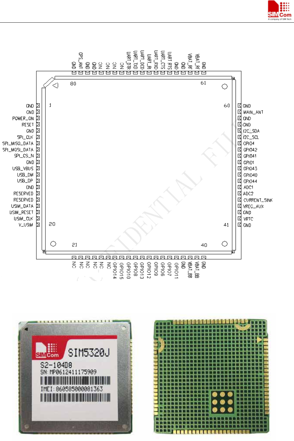
There are 80 pins on SIM5320J, which provide most application interfaces for customers’ board.

SIM5320J Document
- 2 -
1.2. Feature
● Dual-Band UMTS/HSDPA 850/2100MHz
● Duad-Band GSM/GPRS/EDGE 900/1800MHz
● GPRS multi-slot class 12
● EDGE multi-slot class 12
● Output power
- UMTS 850/2100: 0.25W
- GSM900: 2W
- DCS1800: 1W
● Control Via AT Commands
● Supply voltage range: 3.4~ 4.2V
● Extended operation temperature: -40℃ to +85℃
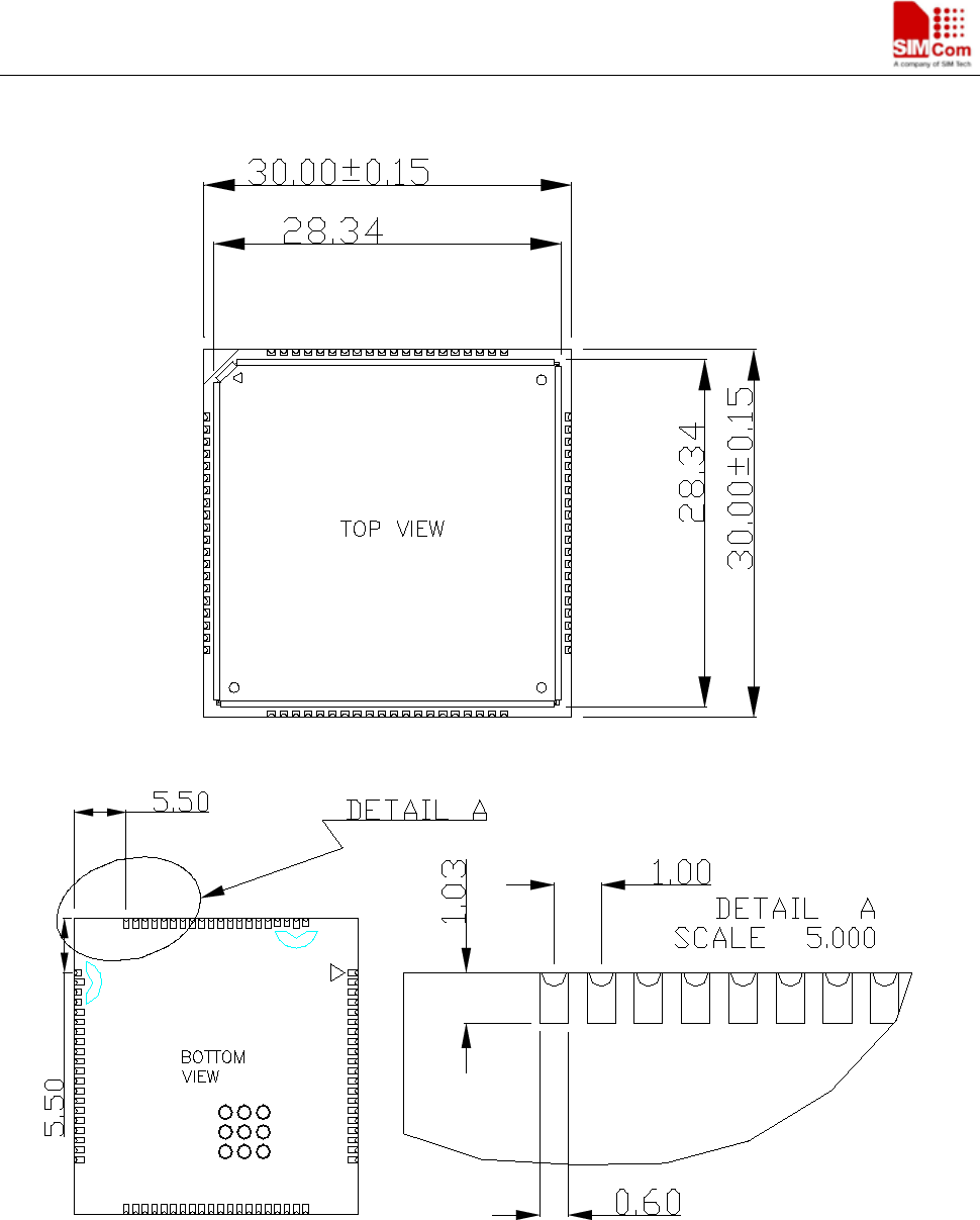
● Dimension: 30 * 30 * 2.9 mm
● Weight: 5.6g
● 80 LCC pads include
– Interface to external SIM 3V/1.8V
– USB 2.0
– UART
– I2C
– Keypad
– SPI
– PCM
– GPIO
– ADC
SIM5320J Document
- 3 -
1.3. Pin
1.4. Picture
Figure 1: Top and Bottom view of SIM5320J
SIM5320J Document
- 4 -
1.5. Dimension
Figure 2: Dimention
SIM5320J Document
- 5 -
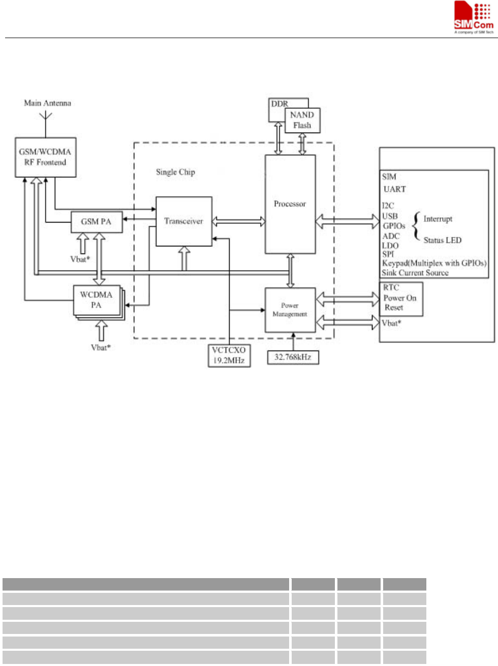
2. Detail Block Diagram
Figure 3: Block diagram of SIM5320J
3. Electrical and Reliability Characteristics
3.1. Absolute Maximum Ratings
The absolute maximum ratings stated in following table are stress ratings under non-operating conditions. Stresses
beyond any of these limits will cause permanent damage to SIM5320J.
Table 1: Absolute maximum ratings
Parameter
Min
Max
Unit
Voltage at digital pins (1.8v mode)
-0.3
1.8+0.3
V
Voltage at digital pins (2.6v mode)
-0.3
2.6+0.3
V
Voltage at VBAT
-0.5
6.0
V
Voltage at VRTC
1.5
3.2
V
Voltage at USB_VBUS
-0.5
6.0
V
3.2. USIM Card Interface Characteristics
Table 2: USIM card interface characteristics
SIM5320J Document
- 6 -
3.3. SIM_VDD Characteristics
3.4. Current Consumption (VBAT = 3.8V)
Table 3: Current consumption
GSM Sleep mode (without USB connection)
GSM900
Sleep @DRX=2 4.5mA
Sleep @DRX=5 2.7mA
Sleep @DRX=9 2.3mA
DCS1800
Sleep @DRX=2 4.5mA
Sleep @DRX=5 2.7mA
Sleep @DRX=9 2.3mA
GSM Sleep Mode (with USB suspended)
GSM900
Sleep @DRX=2 4.6mA
Sleep @DRX=5 2.8mA
Sleep @DRX=9 2.5mA
DCS1800
Sleep @DRX=2 4.6mA
Sleep @DRX=5 2.8mA
Sleep @DRX=9 2.5mA
DATA mode, GPRS ( 1 Rx,4 Tx ) CLASS 12
GSM 900
@power level #5 <660mA,Typical 484mA
DCS1800
@power level #0 <530mA,Typical 346mA
DATA mode, GPRS ( 3Rx, 2 Tx ) CLASS 12
GSM 900
@power level #5 <440mA,Typical 332mA
DCS1800
@power level #0 <400mA,Typical 260mA
EDGE Data
DATA mode, EDGE( 1 Rx,4 Tx ) CLASS 12
GSM 900
@power level #8 <500mA,Typical 332mA
DCS1800
@power level #2 <450mA,Typical 291mA
DATA mode, EDGE( 3Rx, 2 Tx ) CLASS 12
GSM 900
@power level #8 <330mA,Typical 231mA
DCS1800
@power level #2 <300mA,Typical 206mA
UMTS Sleep Mode (without USB connection)
WCDMA 2100
Sleep @DRX=9 2.2mA
Pin name 3.0V mode 1.8V mode
Min Typ Max Min Typ Max
V_USIM 2.7 3.00 3.3 1.65 1.8 2.0
USIM_RESET
0.8* V_USIM
3.00
V_USIM
0.8* V_USIM
1.8
V_USIM
USIM_CLK 0.7* V_USIM 3.00 V_USIM 0.8* V_USIM 1.8 V_USIM
USIM_DATA
0.7* V_USIM
3.00
V_USIM
0.8* V_USIM
1.8
V_USIM
SIM5320J Document
- 7 -
Sleep @DRX=8 2.7 mA
Sleep @DRX=6 4.7mA
WCDMA 850
Sleep @DRX=9 2.2mA
Sleep @DRX=8 2.7 mA
Sleep @DRX=6 4.7mA
UMTS Sleep Mode (with USB suspended)
WCDMA 2100
Sleep @DRX=9 2.4mA
Sleep @DRX=8 2.8 mA
Sleep @DRX=6 4.8mA
WCDMA 850
Sleep @DRX=9 2.4mA
Sleep @DRX=8 2.8 mA
Sleep @DRX=6 4.8mA
HSDPA Data
WCDMA 2100
@Power 23dBm CQI=22 Typical 610mA
@Power 21dBm CQI=5 Typical 540mA
@Power -5dBm CQI=22 Typical 270mA
WCDMA 850
@Power 23dBm CQI=22 Typical 550mA
@Power 21dBm CQI=5 Typical 490mA
@Power -5dBm CQI=22 Typical 220mA
3.5. Electro-Static Discharge
SIM800H is an ESD sensitive component, so more attention should be paid to the procedure of handling and
packaging. The ESD test results are shown in the following table.
Table 4: The ESD characteristics (Temperature: 25℃, Humidity: 45 %)
Part
Contact discharge
Air discharge
VBAT,GND
±4KV
±6KV
UART,USB
±2KV
±6KV
Antenna port
±4KV
±6KV
Other ports
±2KV
±2KV
4. Radio Characteristics
4.1. Module RF Output Power
The following table shows the module conducted output power.
Table 5: SIM5320J conducted RF output power
Frequency
Max
Min
E-GSM900
33dBm ±2dB
5dBm ± 5dB
SIM5320J Document
- 8 -
DCS1800
30dBm ±2dB
0dBm ± 5dB
E-GSM900 (8-PSK)
27dBm ±3dB
5dBm ± 5dB
DCS1800 (8-PSK)
26dBm +3/-4dB
0dBm ±5dB
WCDMA 2100
24dBm +1/-3dB
-56dBm ±5dB
WCDMA 850
24dBm +1/-3dB
-56dBm ±5dB
4.2. Module RF Receive Sensitivity
The following table shows the module’s conducted receive sensitivity, it is tested under static condition.
Table 6: SIM5320J conducted RF receive sensitivity
Frequency
Receive sensitivity
E-GSM900
< -106dBm
DCS1800
< -106dBm
WCDMA 2100
< -108dBm
WCDMA 850
< -106dBm
4.3. Module Operating Frequencies
The following table shows the module’s operating frequency range.
Table 7: SIM5320J operating frequencies
Frequency
Receiving
Transmission
E-GSM900
925
~
960 MHz
880
~
915 MHz
DCS1800
1805
~
1880 MHz
1710
~
1785 MHz
WCDMA2100
2110
~
2170 MHz
1920
~
1980 MHz
WCDMA 850
869
~
894 MHz
824
~
849 MHz
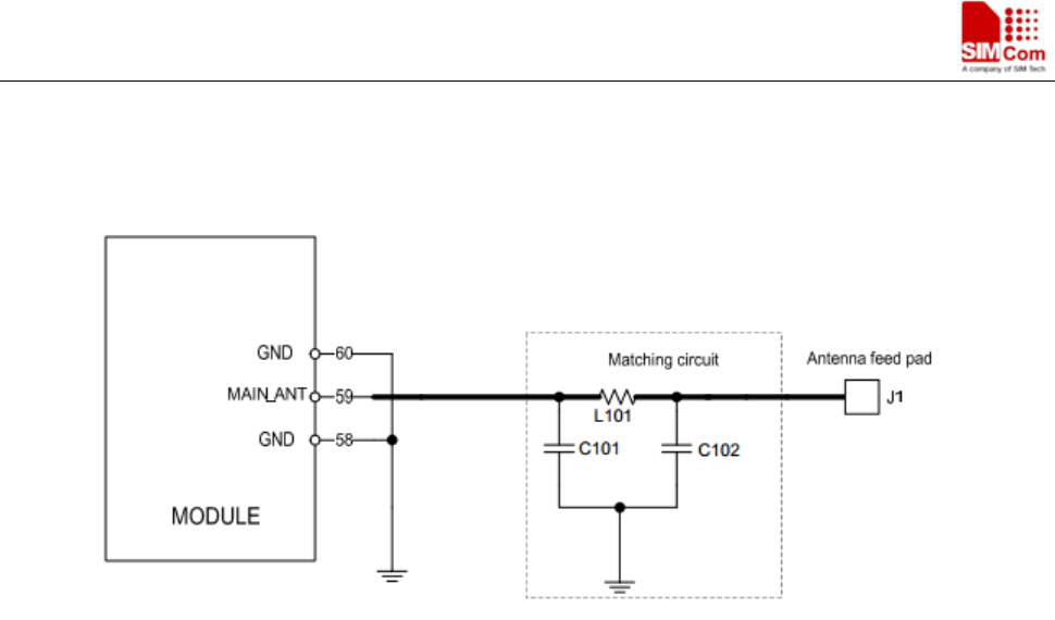
5. Antenna interface
SIM5320J provides RF antenna interface. Customer’s antenna should be located in the host board and
connected to module’s antenna pad through micro-strip line or other types of RF trace and the trace impedance
must be controlled in 50Ω.The maximum gain of the GSM antenna gain should not exceed 2dBi considering the
SAR radio. SIMCom recommends that the total insertion loss between the antenna pad and antenna should meet
the following requirements:
● GSM900<0.5dB
● DCS1800 <0.9dB
● WCDMA 2100<0.9dB
● WCDMA 850<0.5dB
SIM5320J Document
- 9 -
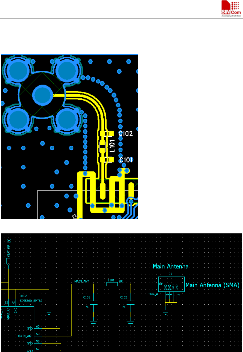
To facilitate the antenna tuning and certification test, a RF connector and an antenna matching circuit should be
added. The following figure is the recommended circuit.
Figure1: antenna matching circuit
In this figure, the components L101,C101,C102 is used for antenna matching, the value of components can only
be got after the antenna tuning, usually, they are provided by antenna vendor. By default, the L101 is 0 ohm
resistors, and the C101, C102 are reserved for tuning.
The RF test connector in the figure is used for the conducted RF performance test, and should be placed as close
as to the module’s antenna pin. The traces impedance between components must be controlled in 50ohm.
SIM5320J Document
- 10 -
5.1 Dipole Antenna Reference Design PCB
Mount these devices with brown mark facing up. Units: mm
Line width should be designed to provide 50Ω im ped a nc e matching characteristics
5.2 Dipole Antenna Reference Design Schematic