Simcom 2011091310088 GSM/GPRS/GPS Module User Manual SIM908 Rev 3
Shanghai Simcom Ltd. GSM/GPRS/GPS Module SIM908 Rev 3
UserManual.wiki
>
Simcom
>
2011091310088 User Manual
Users Manual
Navigation menu
Upload a User Manual
Namespaces
Wiki Guide
HTML
PDF
Info
Views
User Manual
Discussion / Help
Navigation
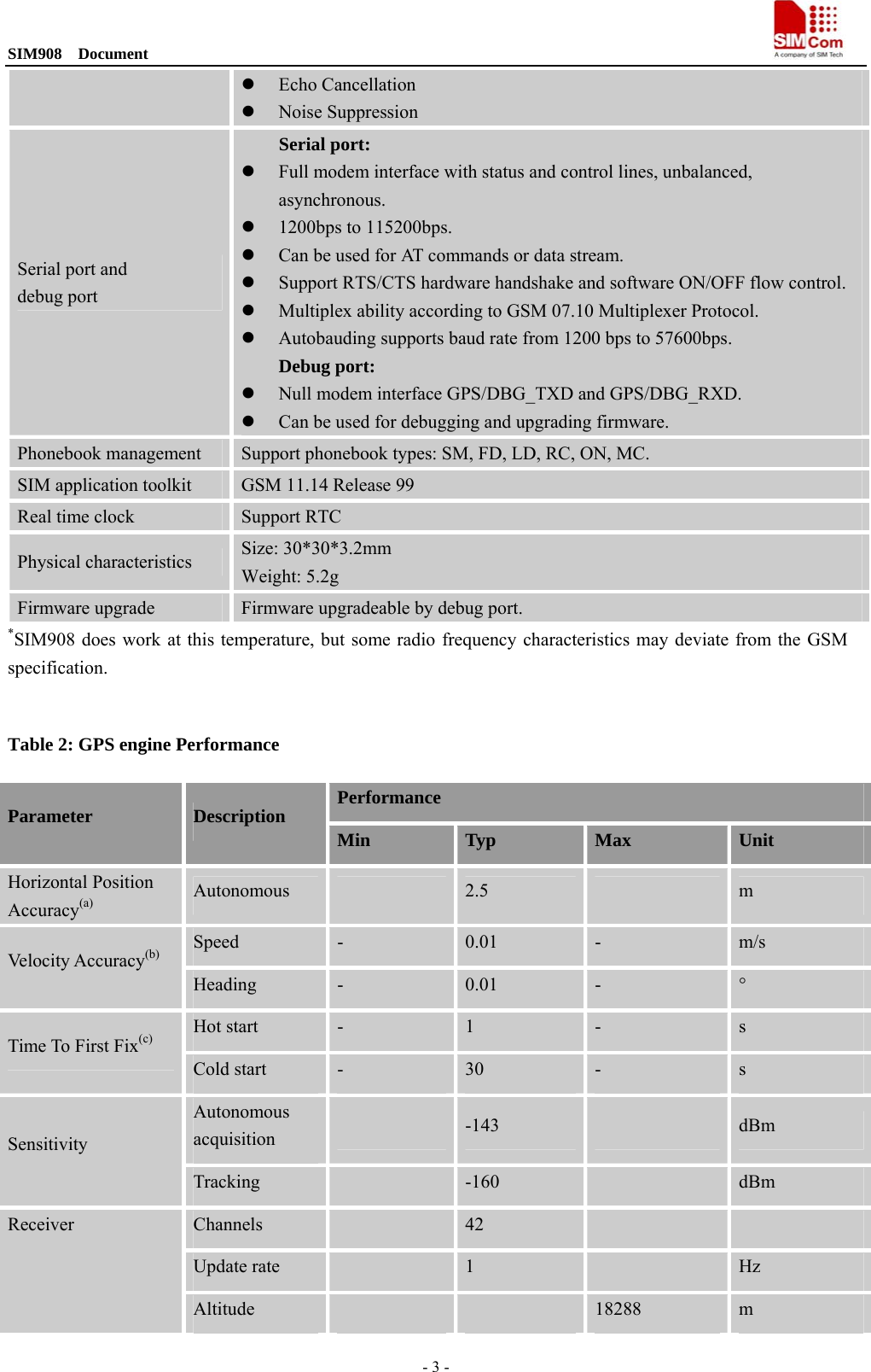
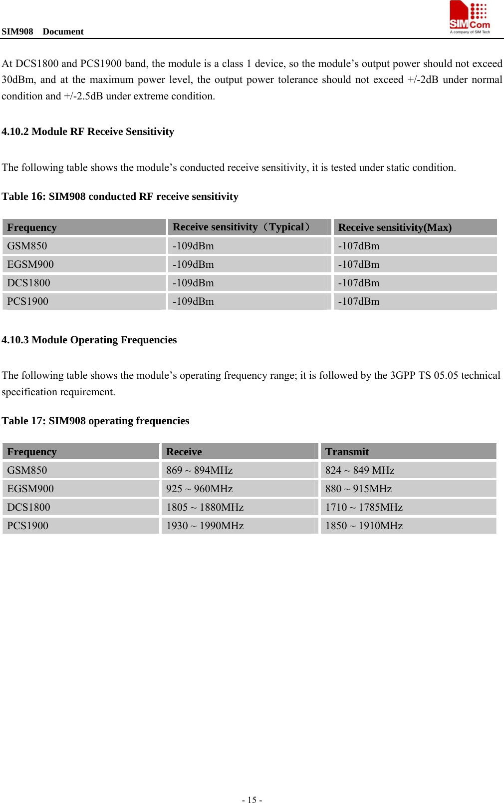
![SIM908 Document - 2 - mode (GPS engine is powered down). SIM908 integrates TCP/IP protocol and extended TCP/IP AT commands which are very useful for data transfer applications. 1.2 SIM908 Key Features Table 1: SIM908 GSM/GPRS engine key features Feature Implementation Power supply 3.4V ~ 4.5V Power saving Typical power consumption in sleep mode is 1.0mA ( BS-PA-MFRMS=9, GPS engine is powered down ) Charging Supports charging control for Li-Ion battery Frequency bands z SIM908 Quad-band: GSM 850, EGSM 900, DCS 1800, PCS 1900. SIM908 can search the 4 frequency bands automatically. The frequency bands also can be set by AT command “AT+CBAND”. For details, please refer to document [1]. z Compliant to GSM Phase 2/2+ Transmitting power z Class 4 (2W) at GSM 850 and EGSM 900 z Class 1 (1W) at DCS 1800 and PCS 1900 GPRS connectivity z GPRS multi-slot class 10(default) z GPRS multi-slot class 8 (option) Temperature range z Normal operation: -20°C ~ +60°C z Restricted operation: -40°C ~ -20°C and +80 °C ~ +60°C* z Storage temperature -45°C ~ +90°C Data GPRS z GPRS data downlink transfer: max. 85.6 kbps z GPRS data uplink transfer: max. 42.8 kbps z Coding scheme: CS-1, CS-2, CS-3 and CS-4 z Integrate the TCP/IP protocol. z Support Packet Broadcast Control Channel (PBCCH) CSD z Support CSD transmission USSD z Unstructured Supplementary Services Data (USSD) support SMS z MT, MO, CB, Text and PDU mode z SMS storage: SIM card FAX Group 3 Class 1 SIM interface Support SIM card: 1.8V, 3V External antenna Antenna pad Audio features Speech codec modes: z Half Rate (ETS 06.20) z Full Rate (ETS 06.10) z Enhanced Full Rate (ETS 06.50 / 06.60 / 06.80) z Adaptive multi rate (AMR)](https://usermanual.wiki/Simcom/2011091310088/User-Guide-1557862-Page-2.png)