Simcom 2011091310088 GSM/GPRS/GPS Module User Manual SIM908 Rev 3
Shanghai Simcom Ltd. GSM/GPRS/GPS Module SIM908 Rev 3
Simcom >
Users Manual

SIM908 Document
- 1 -
SIM908 User Manual
Note: This device complies with part 15 Rules. Operation is subject to the following two conditions: (1) This
device may not cause harmful interference, and (2) this device must accept any interference received, including
interference that may cause undesired operation.
If this equipment is installed in a host, We can find the ID label when opening the host. For label requirement
when transmitter module is installed in a host, the host shall have an additional permanent label referring to the
enclosed module:“Contains Transmitter Module FCC ID: UDV-2011091310088” or “Contains FCC ID:
UDV-2011091310088”.
This equipment has a GSM antenna and a GPS antenna, the GPS antenna peak gain is 5 dBi and modulation
type is BPSK; the GSM antenna peak gain is 3 dBi and modulation type is GMSK.
WARNING: Changes or modifications to this unit not expressly approved by the party responsible for
compliance could void the user's authority to operate the equipment. The antenna of the product, under normal
use condition is at least 24.22 cm away from the body of the user,the user must keeping at least 24.22cm
distance to the antenna.
The device has been evaluated to meet general RF exposure requirement. The device can be used in portable
exposure condition without restriction.
1. SIM908 Description
1.1 Summarize
Designed for global market, SIM908 is integrated with a high performance GSM/GPRS engine and a GPS engine.
The GSM/GPRS engine is a quad-band GSM/GPRS module that works on frequencies GSM 850MHz, EGSM
900MHz, DCS 1800MHz and PCS 1900MHz. SIM908 features GPRS multi-slot class 10/ class 8 (optional) and
supports the GPRS coding schemes CS-1, CS-2, CS-3 and CS-4. The GPS solution offers best- in-class
acquisition and tracing sensitivity, Time-To-First-Fix (TTFF) and accuracy.
With a tiny configuration of 30*30*3.2mm, SIM908 can meet almost all the space requirements in user
applications, such as M2M, smart phone, PDA, tracker and other mobile devices.
SIM908 has 80 SMT pads, and provides all hardware interfaces between the module and customers’ boards.
z Serial port and debug port can help user easily develop user’s applications.
z GPS Serial port.
z Two audio channels include two audio inputs and two audio outputs. These can be easily configured by AT
command.
z Charging interface.
z Programmable general purpose input and output.
z The keypad and SPI display interfaces will give users the flexibility to develop customized applications.
z RF pad and connector interface.
SIM908 is designed with power saving technique so that the current consumption is as low as 1.0mA in sleep
SIM908 Document
- 2 -
mode (GPS engine is powered down).
SIM908 integrates TCP/IP protocol and extended TCP/IP AT commands which are very useful for data transfer
applications.
1.2 SIM908 Key Features
Table 1: SIM908 GSM/GPRS engine key features
Feature Implementation
Power supply 3.4V ~ 4.5V
Power saving Typical power consumption in sleep mode is 1.0mA ( BS-PA-MFRMS=9, GPS
engine is powered down )
Charging Supports charging control for Li-Ion battery
Frequency bands
z SIM908 Quad-band: GSM 850, EGSM 900, DCS 1800, PCS 1900. SIM908
can search the 4 frequency bands automatically. The frequency bands also
can be set by AT command “AT+CBAND”. For details, please refer to
document [1].
z Compliant to GSM Phase 2/2+
Transmitting power
z Class 4 (2W) at GSM 850 and EGSM 900
z Class 1 (1W) at DCS 1800 and PCS 1900
GPRS connectivity
z GPRS multi-slot class 10(default)
z GPRS multi-slot class 8 (option)
Temperature range
z Normal operation: -20°C ~ +60°C
z Restricted operation: -40°C ~ -20°C and +80 °C ~ +60°C*
z Storage temperature -45°C ~ +90°C
Data GPRS
z GPRS data downlink transfer: max. 85.6 kbps
z GPRS data uplink transfer: max. 42.8 kbps
z Coding scheme: CS-1, CS-2, CS-3 and CS-4
z Integrate the TCP/IP protocol.
z Support Packet Broadcast Control Channel (PBCCH)
CSD z Support CSD transmission
USSD z Unstructured Supplementary Services Data (USSD) support
SMS
z MT, MO, CB, Text and PDU mode
z SMS storage: SIM card
FAX Group 3 Class 1
SIM interface Support SIM card: 1.8V, 3V
External antenna Antenna pad
Audio features
Speech codec modes:
z Half Rate (ETS 06.20)
z Full Rate (ETS 06.10)
z Enhanced Full Rate (ETS 06.50 / 06.60 / 06.80)
z Adaptive multi rate (AMR)
SIM908 Document
- 3 -
z Echo Cancellation
z Noise Suppression
Serial port and
debug port
Serial port:
z Full modem interface with status and control lines, unbalanced,
asynchronous.
z 1200bps to 115200bps.
z Can be used for AT commands or data stream.
z Support RTS/CTS hardware handshake and software ON/OFF flow control.
z Multiplex ability according to GSM 07.10 Multiplexer Protocol.
z Autobauding supports baud rate from 1200 bps to 57600bps.
Debug port:
z Null modem interface GPS/DBG_TXD and GPS/DBG_RXD.
z Can be used for debugging and upgrading firmware.
Phonebook management Support phonebook types: SM, FD, LD, RC, ON, MC.
SIM application toolkit GSM 11.14 Release 99
Real time clock Support RTC
Physical characteristics Size: 30*30*3.2mm
Weight: 5.2g
Firmware upgrade Firmware upgradeable by debug port.
*SIM908 does work at this temperature, but some radio frequency characteristics may deviate from the GSM
specification.
Table 2: GPS engine Performance
Performance
Parameter Description Min Typ Max Unit
Horizontal Position
Accuracy(a)
Autonomous 2.5 m
Speed - 0.01 - m/s
Velocity Accuracy(b)
Heading - 0.01 - °
Hot start - 1 - s
Time To First Fix(c)
Cold start - 30 - s
Autonomous
acquisition -143 dBm
Sensitivity
Tracking -160 dBm
Channels 42
Update rate 1 Hz
Receiver
Altitude 18288 m
SIM908 Document
- 4 -
Velocity 1850 km/h
Tracking L1,
CA Code
Protocol support
NMEA,OSP
Continuous
tracking
76 mA
acquisition 77
Power consumption(d)
Power down
current
0.03 uA
Table 3: Coding schemes and maximum net data rates over air interface
Coding scheme 1 timeslot 2 timeslot 4 timeslot
CS-1 9.05kbps 18.1kbps 36.2kbps
CS-2 13.4kbps 26.8kbps 53.6kbps
CS-3 15.6kbps 31.2kbps 62.4kbps
CS-4 21.4kbps 42.8kbps 85.6kbps
SIM908 Document
- 5 -
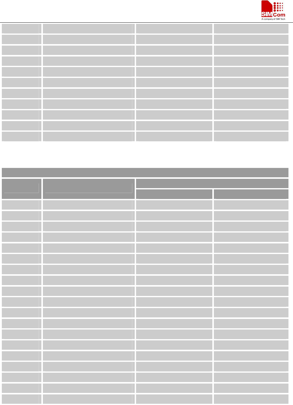
2. Package Information
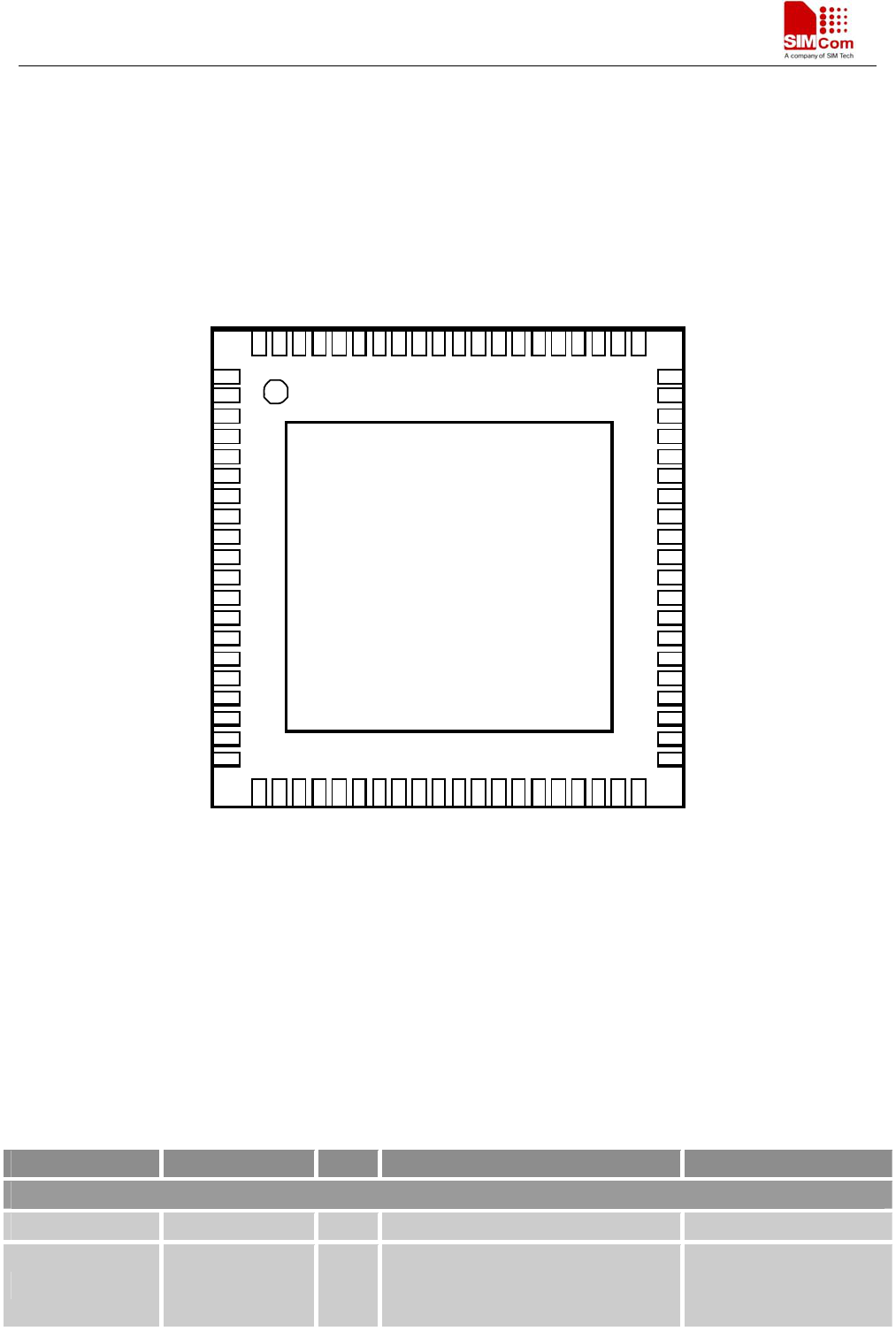
2.1 Pin out Diagram
GND
GPS-ANT
GND
GND
GPS-VANT-IN
GPS-VANT-OUT
VCHG
TEMP-BAT
DTR
TXD
DCD
RI
RXD
CTS
RTS
GND
GND
VBAT
VBAT
GND
GND GND
GND GSM-ANT
PWRKE
Y
GND
NC GND
GND I2C-SD
A
DISP-CLK I2C-SCL
DISP-DAT
A
N
C
DIS P-D/C N
C
DISP-CS STATUS
GND NETLIGHT
PWM3
PWM2
PWM1
ADC
N
C
GPS/DBG-RXD N
C
SIM-DAT
A
VDD-EXD
SIM-RST GND
SIM-CLK VRT
C
SIM-VDD GND
SPK1N
SPK1P
MI C1P
MIC1N
SPK2N
SPK2P
MIC2P
MIC2N
NC
NC
GPIO1/KBR0
GPIO2/KBR1
GPIO3/KBR2
GPIO4/KBC0
GPIO5/KBC1
GPIO6/KBC2
GND
NC
NC
GND
63
62
61
38
39
40
18
19
20
43
42
41
37
33
34
35
36
29
30
31
32
2
5
26
27
2
8
21
22
23
24
17 44
16 45
15 46
14 47
SIM908
TOP VIEW
13 48
12 49
10 51
11 50
952
853
754
655
556
457
3
58
2
59
64
160
68
67
66
6
5
72
71
70
69
76
75
74
73
80
79
78
77
GPS/DBG-TXD
NC
NC
NC
GND
Figure 1: SIM908 pin out diagram (Top view)
2.2 Pin Description
Table 4: Pin description
Pin name Pin number I/O Description Comment
Power supply
VBAT 62, 63 I Power supply 3.2V ~ 4.8V
VRTC 42 I/O Power supply for RTC
It is recommended to
connect with a battery or
a capacitor (e.g. 4.7uF).
SIM908 Document
- 6 -
VDD-EXT 44 O 2.8V output power supply If it is unused, keep open.
GPS-VANT-OUT 75 O 2.8V output for GPS active antenna If it is unused, keep open.
GPS-VANT-IN 76 I GPS active antenna power supply If it is unused, keep open.
GND
1, 2, 5, 10, 14, 37,
40, 41, 43, 57, 58,
60, 61, 64, 65, 77,
78, 80
Ground
Charge interface
VCHG 74 I Charger input
TEMP_BAT 73 I Battery temperature sensor
Power on/down
PWRKEY 3 I
PWRKEY should be pulled low at
least 1 second and then released to
power on/down the module.
Pulled up internally.
Audio interfaces
MIC1P 23
MIC1N 24
I Differential audio input
SPK1P 22
SPK1N 21
O Differential audio output
MIC2P 27
MIC2N 28
I Differential audio input
SPK2N 25
SPK2P 26
O Differential audio output
If these pins are unused,
keep open.
Status
STATUS 52 O Power on status
NETLIGHT 51 O Network status
If these pins are unused,
keep open.
LCD interface
DISP -CLK 6 O
DISP-DATA 7 I/O
DISP -D/C 8 O
DISP -CS 9 O
Display interface If these pins are unused,
keep open.
I2C interface
I2C-SDA 56 O I2C serial bus data
I2C-SCL 55 I/O I2C serial bus clock
If these pins are unused,
keep open.
Keypad interface / GPIOs
GPIO1/KBR0 31 GPIO1/keypad row 0
GPIO2/KBR1 32 GPIO2/keypad row 1
GPIO3/KBR2 33
I/O
GPIO3/keypad row 2
If these pins are unused,
keep open.
SIM908 Document
- 7 -
GPIO4/KBC0 34 GPIO4/keypad column 0
GPIO5/KBC1 35 GPIO5/keypad column 1
GPIO6/KBC2 36 GPIO6/keypad column 3
Serial port
RXD 68 I Receive data
TXD 71 O Transmit data
RTS 66 O Request to send
CTS 67 I Clear to send
DCD 70 O Data carrier detect
RI 69 O Ring indicator
DTR 72 I Data terminal ready
If only TXD and RXD
are used, it is suggested
to pull down DTR, and
others pins can be kept
open.
GPS/Debug interface
GPS/DBG-TXD 15 O
GPS/DBG-RXD 16 I
For GPS NMEA information output ,
debugging and upgrading firmware
If these pins are unused,
keep open.
SIM interface
SIM-VDD 20 O Voltage supply for SIM card. Support
1.8V or 3V SIM card
SIM-DATA 17 I/O SIM data input/output
SIM-CLK 19 O SIM clock
SIM-RST 18 O SIM reset
All signals of SIM
interface should be
protected against ESD
with a TVS diode array.
ADC
ADC 47 I Input voltage range: 0V ~ 2.8V If it is unused, keep open.
Pulse width modulation( PWM )
PWM1 48 O PWM
PWM2 49 O PWM
PWM3 50 O PWM
If these pins are unused,
keep open.
GSM/GPS RF interface
GSM-ANT 59 I/O GSM radio antenna connection Impendence must be
controlled to 50Ω.
GPS-ANT 79 I GPS radio antenna connection Impendence must be
controlled to 50Ω.
Not connect
NC 4,11,12,13,29,30,
38,39,45,46,53,54 - These pins should be
kept open.
SIM908 Document
- 8 -
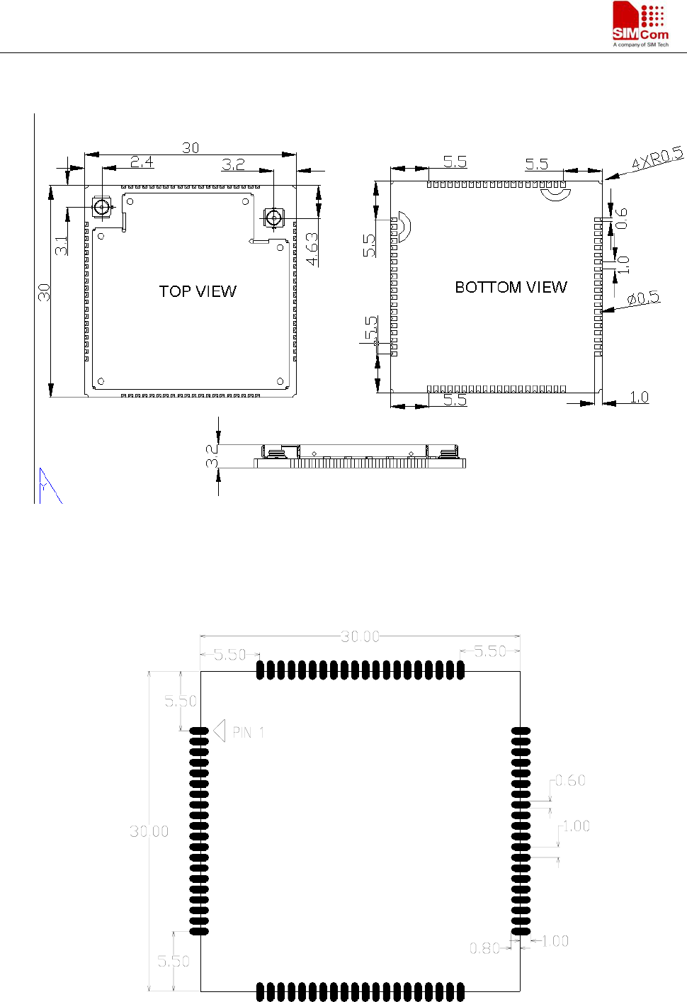
2.3 Package Dimensions
Figure 2: Dimensions of SIM908(Unit: mm)
Figure 3: Recommended PCB footprint outline(Unit: mm)
SIM908 Document
- 9 -
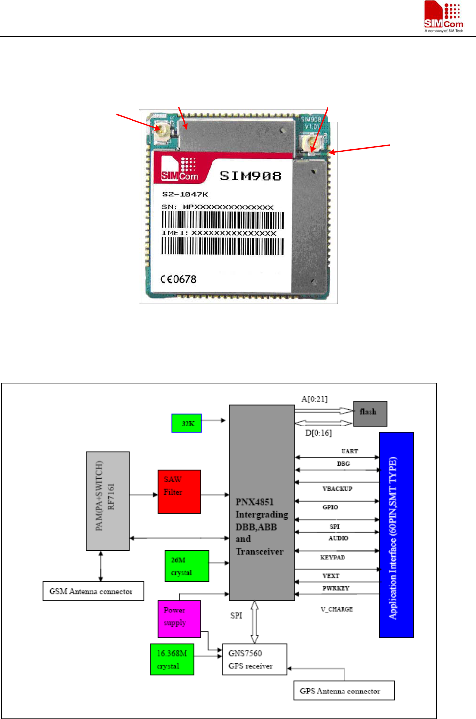
2.4 Pictures
Figure 4: The RF interface of module
3. Detail Block Diagram
Figure 5: Block diagram of SIM908
GPS
Antenna connector
GPS PAD GSM
Antenna connector
GSM PAD
SIM908 Document
- 10 -
4. Electrical and Reliability Characteristics
4.1 Absolute Maximum Ratings
The absolute maximum ratings stated in following table are stress ratings under non-operating conditions. Stresses
beyond any of these limits will cause permanent damage to SIM908.
Table 5: Absolute maximum ratings
Symbol Parameter Min Typ Max Unit
VBAT Power supply voltage - - 5.5 V
VI
* Input voltage -0.3 - 3.1 V
II
* Input current - - 10 mA
IO
* Output current - - 10 mA
*These parameters are for digital interface pins, such as keypad, GPIO, I2C, UART, LCD, PWMs and DEBUG.
4.2 Recommended Operating Conditions
Table 6: Recommended operating conditions
Symbol Parameter Min Typ Max Unit
VBAT Power supply voltage 3.2 4.0 4.8 V
TOPER Operating temperature -40 +25 +85 ℃
TSTG Storage temperature -45 +90 ℃
4.3 Digital Interface Characteristics
Table 7: Digital interface characteristics
Symbol Parameter Min Typ Max Unit
IIH High-level input current -10 - 10 uA
IIL Low-level input current -10 - 10 uA
VIH High-level input voltage 2.4 - - V
VIL Low-level input voltage - - 0.4 V
VOH High-level output voltage 2.7 - - V
VOL Low-level output voltage - - 0.1 V
* These parameters are for digital interface pins, such as keypad, GPIO, I2C, UART, LCD, PWMs and DEBUG.
SIM908 Document
- 11 -
4.4 SIM Card Interface Characteristics
Table 8: SIM card interface characteristics
Symbol Parameter Min Typ Max Unit
IIH High-level input current -10 - 10 uA
IIL Low-level input current -10 - 10 uA
1.4 - - V
VIH High-level input voltage
2.4 - - V
- - 0.4 V
VIL Low-level input voltage
2.4 V
1.7 - - V
VOH High-level output voltage
2.7 - - V
- - 0.1 V
VOL Low-level output voltage
- - 0.1 V
4.5 VDD_EXT Characteristics
Table 9: VDD_EXT characteristics
Symbol Parameter Min Typ Max Unit
VO Output voltage 2.70 2.80 2.95 V
IO Output current - - 10 mA
4.6 SIM_VDD Characteristics
Table 10: SIM_VDD characteristics
Symbol Parameter Min Typ Max Unit
2.75 2.9 3.00
VO Output voltage
1.65 1.80 1.95
V
IO Output current - - 10 mA
4.7 VRTC Characteristics
Table 11: VRTC characteristics
Symbol Parameter Min Typ Max Unit
VRTC-IN VRTC input voltage 2.00 3.00 3.15 V
SIM908 Document
- 12 -
IRTC-IN VRTC input current - 2 - uA
VRTC-OUT VRTC output voltage - 3.00 - V
IRTC-OUT VRTC output current - 10 - uA
4.8 Current Consumption (VBAT = 3.8V, GPS engine is powered down)
Table 12: GSM current consumption
Symbol Parameter Conditions Value Unit
IVRTC VRTC current VBAT disconnects. Backup battery is 3 V 2 uA
Power down mode 50 uA
BS-PA-MFRMS=9 1.2
BS-PA-MFRMS=5 1.5
Sleep mode
BS-PA-MFRMS=2 1.7
mA
GSM 850
EGSM 900
DCS 1800
Idle mode
PCS 1900
21 mA
PCL=5 240
PCL=12 110
GSM 850
EGSM 900
PCL=19 76
PCL=0 180
PCL=7 89
Voice call
DCS 1800
PCS 1900
PCL=15 76
mA
PCL=5 240
PCL=12 110
GSM 850
EGSM 900
PCL=19 83
mA
PCL=0 170
PCL=7 95
Data mode
GPRS(1Rx,1Tx)
DCS 1800
PCS 1900
PCL=15 80
mA
PCL=5 270
PCL=12 150
GSM 850
EGSM 900
PCL=19 120
mA
PCL=0 210
PCL=7 130
Data mode
GPRS(4Rx,1Tx)
DCS 1800
PCS 1900
PCL=15 115
mA
PCL=5 435
PCL=12 185
IVBAT VBAT current
Data mode
GPRS(3Rx,2Tx) GSM 850
EGSM 900
PCL=19 130
mA
SIM908 Document
- 13 -
PCL=0 320
PCL=7 155
DCS 1800
PCS 1900
PCL=15 122
mA
IVBAT-peak Peak current During Tx burst 2 A
4.9 Electro-Static Discharge
SIM908 is an ESD sensitive component, so more attention should be paid to the procedure of handling and
packaging. The ESD test results are shown in the following table.
Table 13: The ESD characteristics (Temperature: 25 , Humidity: 45 %)℃
Pin Contact discharge Air discharge
VBAT ±5KV ±10KV
GND ±4KV ±10KV
RXD, TXD ±3KV ±6KV
Antenna port ±5KV ±10KV
SPKP/ SPKN
MICP/ MICN ±3KV ±8KV
PWRKEY ±3KV ±8KV
4.10 Radio Characteristics
4.10.1 Module RF Output Power
The following table shows the module conducted output power, it is followed by the 3GPP TS 05.05 technical
specification requirement.
Table 14: SIM908 GSM 900 and GSM 850 conducted RF output power
GSM 900 and EGSM 850
Tolerance (dB) for conditions
PCL Nominal output power (dBm) Normal Extreme
0-2 39 ±2 ±2.5
3 37 ±3 ±4
4 35 ±3 ±4
5 33 ±3 ±4
6 31 ±3 ±4
7 29 ±3 ±4
8 27 ±3 ±4
SIM908 Document
- 14 -
9 25 ±3 ±4
10 23 ±3 ±4
11 21 ±3 ±4
12 19 ±3 ±4
13 17 ±3 ±4
14 15 ±3 ±4
15 13 ±3 ±4
16 11 ±5 ±6
17 9 ±5 ±6
18 7 ±5 ±6
19-31 5 ±5 ±6
Table 15: SIM908 DCS 1800 and PCS 1900 conducted RF output power
DCS 1800 and PCS 1900
Tolerance (dB) for conditions
PCL Nominal output power (dBm) Normal Extreme
29 36 ±2 ±2.5
30 34 ±3 ±4
31 32 ±3 ±4
0 30 ±3 ±4
1 28 ±3 ±4
2 26 ±3 ±4
3 24 ±3 ±4
4 22 ±3 ±4
5 20 ±3 ±4
6 18 ±3 ±4
7 16 ±3 ±4
8 14 ±3 ±4
9 12 ±4 ±5
10 10 ±4 ±5
11 8 ±4 ±5
12 6 ±4 ±5
13 4 ±4 ±5
14 2 ±5 ±6
15-28 0 ±5 ±6
For the module’s output power, the following is should be noted:
At GSM900 and GSM850 band, the module is a class 4 device, so the module’s output power should not exceed
33dBm, and at the maximum power level, the output power tolerance should not exceed +/-2dB under normal
condition and +/-2.5dB under extreme condition.
SIM908 Document
- 15 -
At DCS1800 and PCS1900 band, the module is a class 1 device, so the module’s output power should not exceed
30dBm, and at the maximum power level, the output power tolerance should not exceed +/-2dB under normal
condition and +/-2.5dB under extreme condition.
4.10.2 Module RF Receive Sensitivity
The following table shows the module’s conducted receive sensitivity, it is tested under static condition.
Table 16: SIM908 conducted RF receive sensitivity
Frequency Receive sensitivity(Typical) Receive sensitivity(Max)
GSM850 -109dBm -107dBm
EGSM900 -109dBm -107dBm
DCS1800 -109dBm -107dBm
PCS1900 -109dBm -107dBm
4.10.3 Module Operating Frequencies
The following table shows the module’s operating frequency range; it is followed by the 3GPP TS 05.05 technical
specification requirement.
Table 17: SIM908 operating frequencies
Frequency Receive Transmit
GSM850 869 ~ 894MHz 824 ~ 849 MHz
EGSM900 925 ~ 960MHz 880 ~ 915MHz
DCS1800 1805 ~ 1880MHz 1710 ~ 1785MHz
PCS1900 1930 ~ 1990MHz 1850 ~ 1910MHz