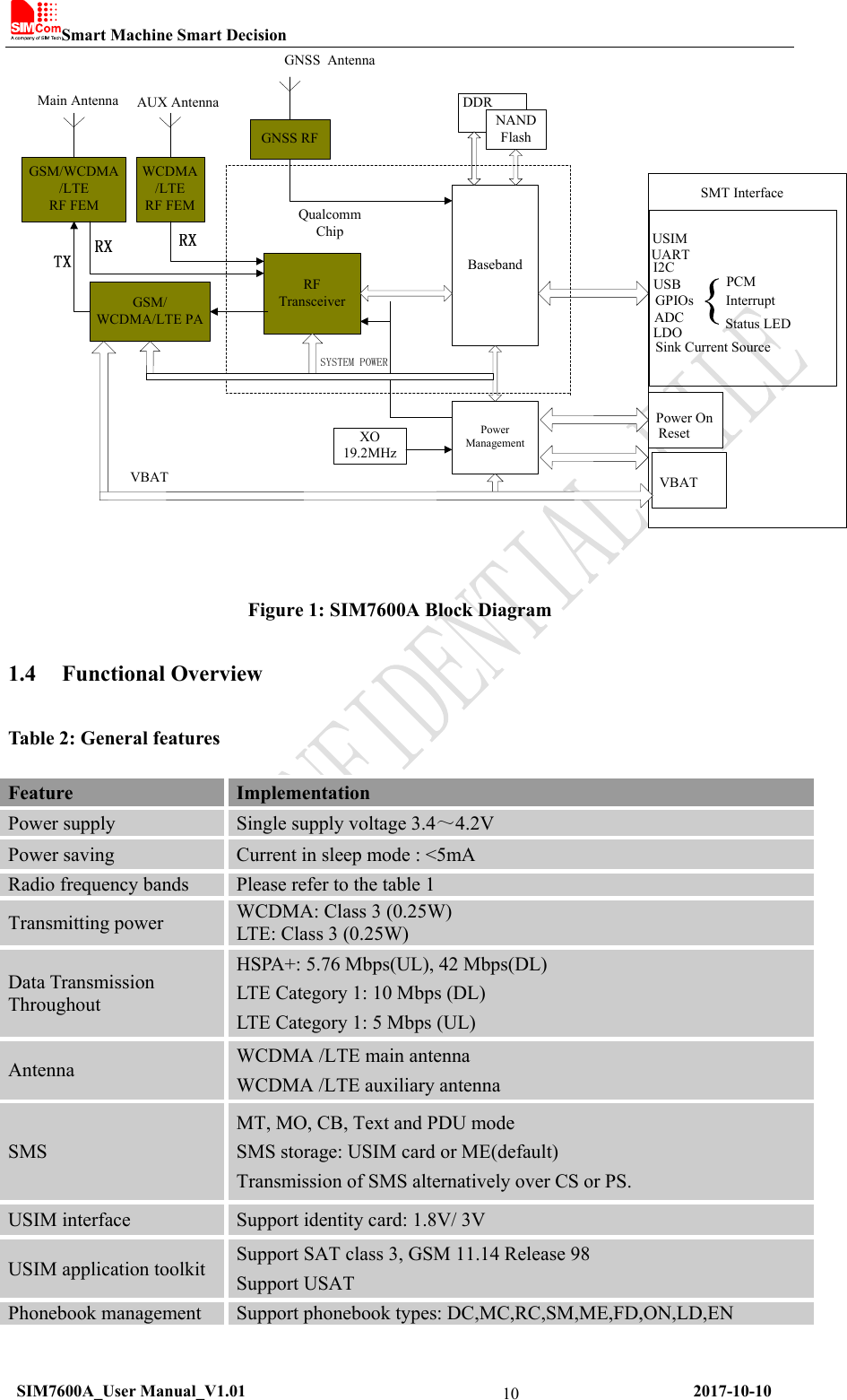
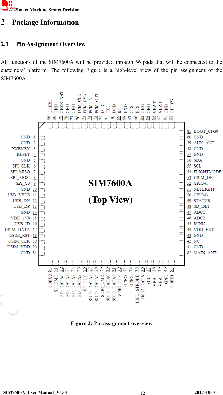
Simcom 201709 LTE-FDD/HSPA MODULE User Manual SIM7600A User Manual V1 01 20171010
Shanghai Simcom Ltd. LTE-FDD/HSPA MODULE SIM7600A User Manual V1 01 20171010
Simcom >
Contents
- 1. SIM7600A_User_Manual_V1.01_20171010
- 2. User Manual
SIM7600A_User_Manual_V1.01_20171010
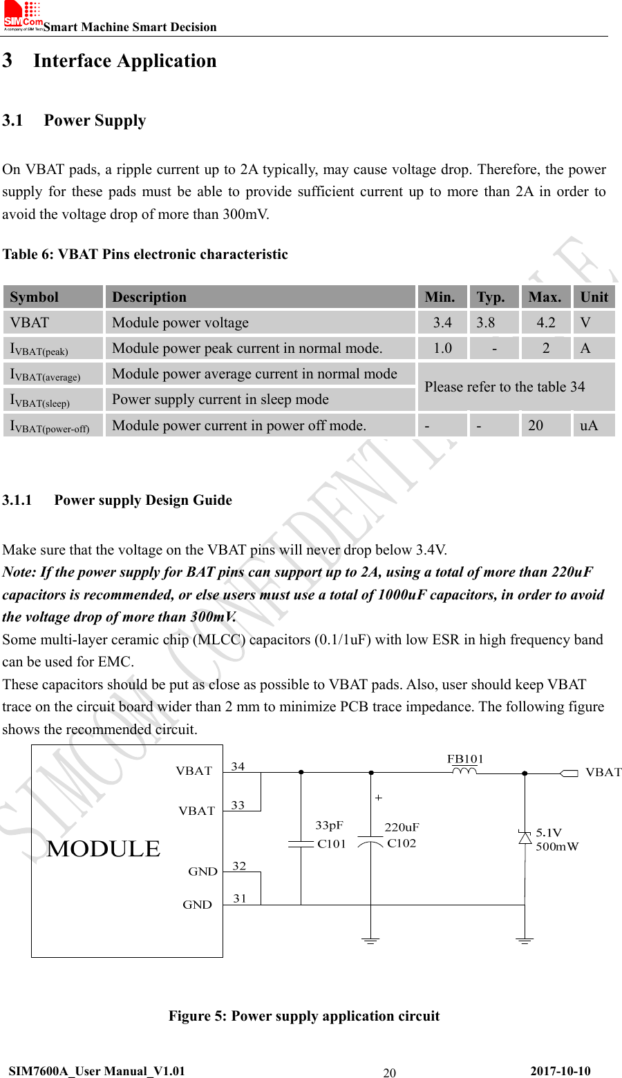
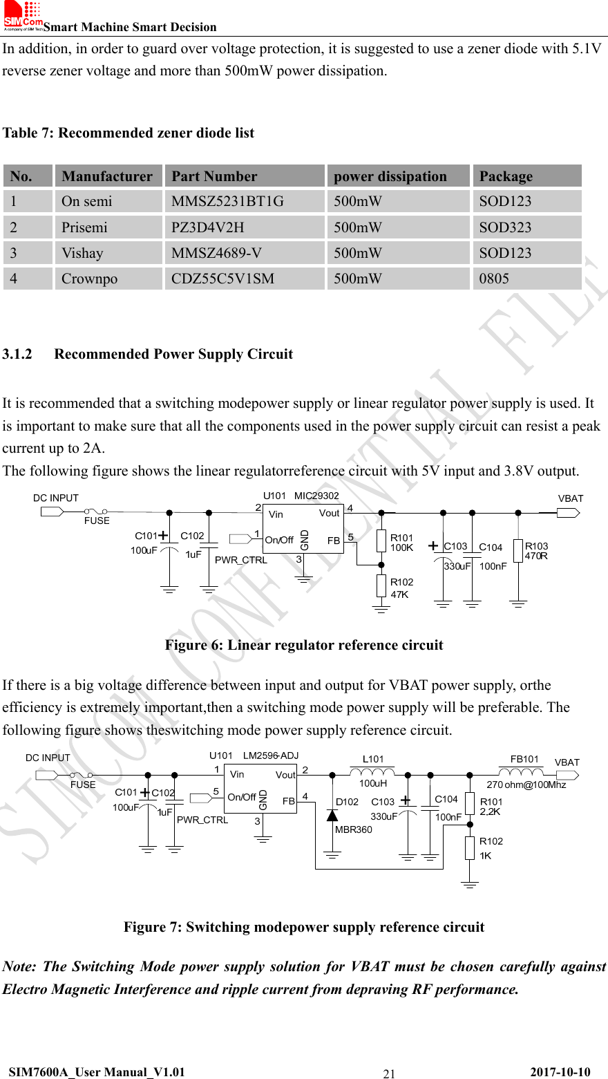
![Smart Machine Smart Decision SIM7600A_User Manual_V1.01 2017-10-10 223.1.3 Voltage Mo nitor To monitor the VBAT voltage, the AT command “AT+CBC” can be used. For monitoring the VBAT voltage outside or within a special range, the AT command “AT+CVALARM” can be used to enable the under-voltage warning function. If users need to power off Module, when the VBAT voltage is out of a range, the AT command “AT+CPMVT” can be used to enable under-voltage power-off function. Note: Under-voltage warning function and under-voltage power-off function are disabled by default. For more information about these AT commands, please refer to Document [1]. 3.2 Power on/Power off/Reset Function 3.2.1 Power on Module can be powered on by pulling the PWRKEY pin down to ground. The PWRKEY pin has been pulled up to dVDDinternally, so you does not need to pull it up externally. It is strongly recommended to put a100nF capacitor and an ESD protection diode close to the PWRKEY pin. Please refer to the following figure for the recommended reference circuit. 47KPWRKEY PowerOn off logicDiodedVDDMODULE100Ω100nF4.7KTurn on /offimpulse Figure 8: ReferencePower on/offCircuit The power-on scenarios are illustrated in the following figure.](https://usermanual.wiki/Simcom/201709.SIM7600A-User-Manual-V1-01-20171010/User-Guide-3598133-Page-22.png)
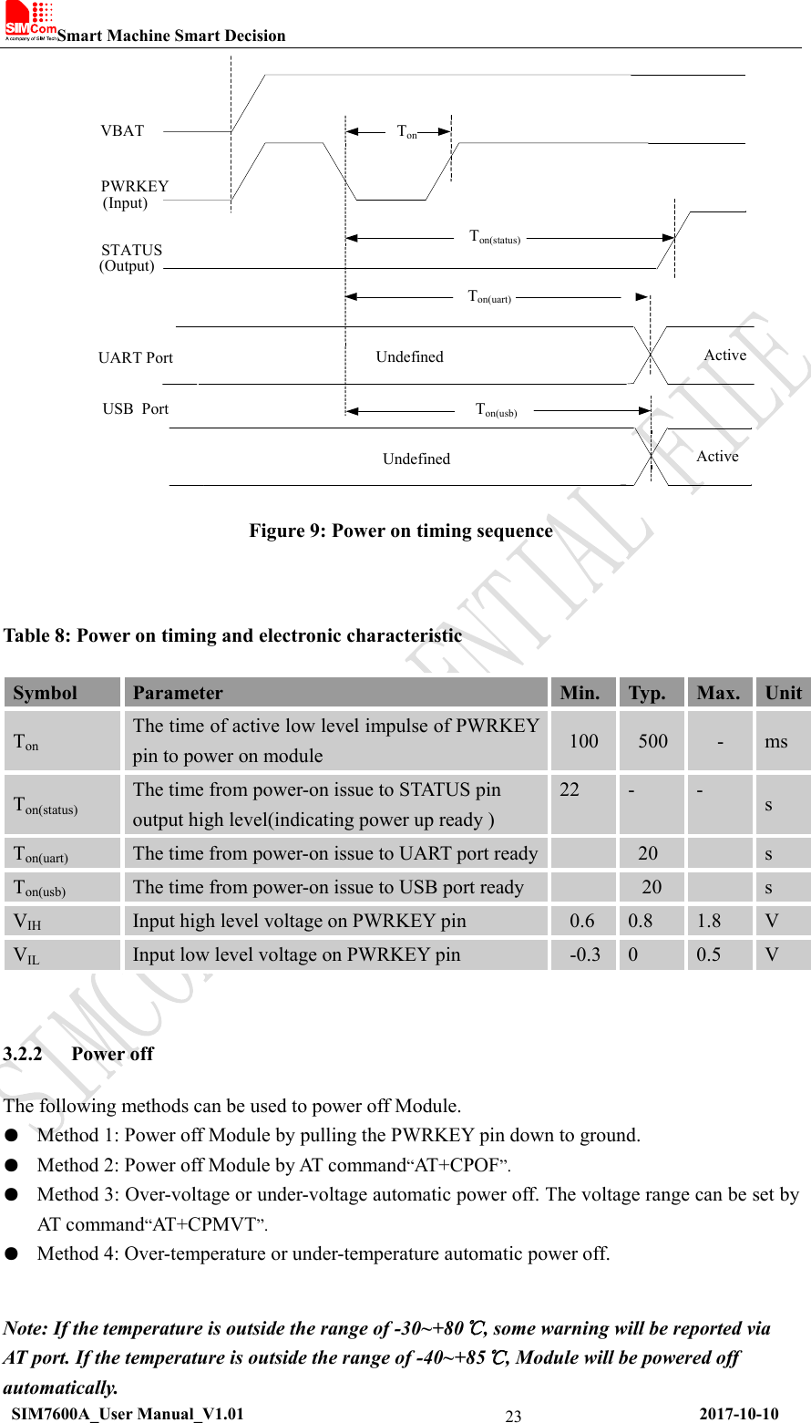
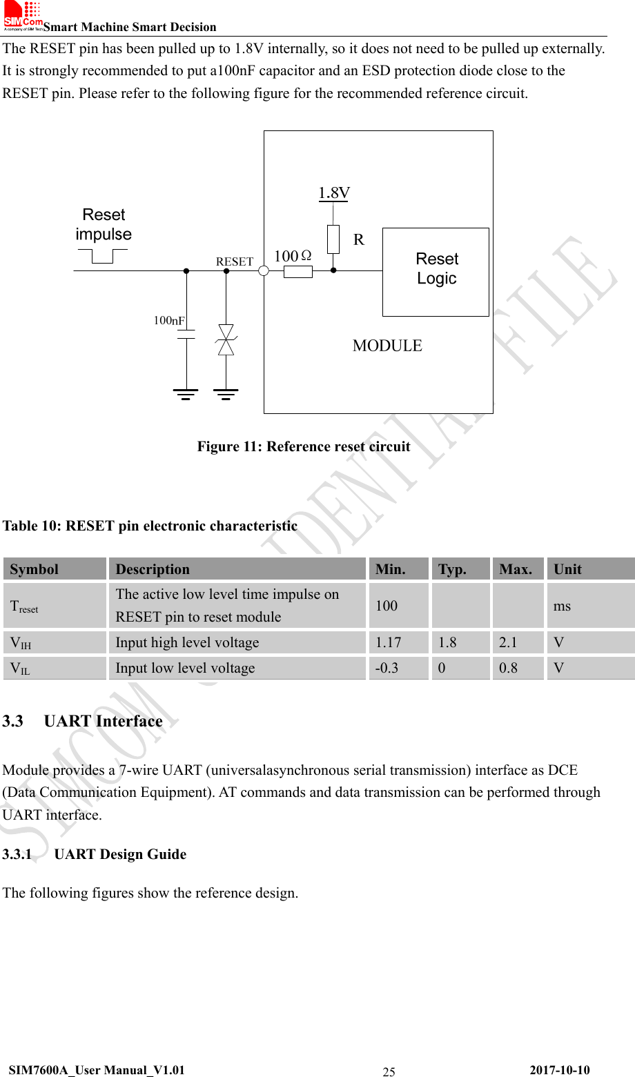
![Smart Machine Smart Decision SIM7600A_User Manual_V1.01 2017-10-10 24For details about “AT+CPOF” and “AT+CPMVT”, please refer to Document [1]. These procedures will make modules disconnect from the network and allow the software to enter a safe state and save data before modules are powered off completely. The power off scenario by pulling down the PWRKEY pin is illustrated in the following figure. (Output)Toff( Input )Toff(status)UART Port UndefinedActiveToff(uart)TonToff-onUSB Port UndefinedActiveToff(usb)PWRKEYSTATUS Figure 10: Power off timing sequence Table 9: Power off timing and Electronic Characteristic Symbol Parameter Time value UnitMin. Typ. Max.Toff The active low level time pulse on PWRKEY pin to power off module 2.5 -- -- s Toff(status) The time from power-off issue to STATUS pin output low level(indicating power off )* 22 - - s Toff(uart) The time from power-off issue to UART port off 15 - - s Toff(usb) The time from power-off issue to USB port off 15 - - s Toff-on The buffer time from power-off issue to power-on issue 0 - - s 3.2.3 Reset Function Module can be reset by pulling the RESET pin down to ground. Note: This function is only used as an emergency reset when AT command “AT+CPOF” and the PWRKEY pin all have lost efficacy.](https://usermanual.wiki/Simcom/201709.SIM7600A-User-Manual-V1-01-20171010/User-Guide-3598133-Page-24.png)
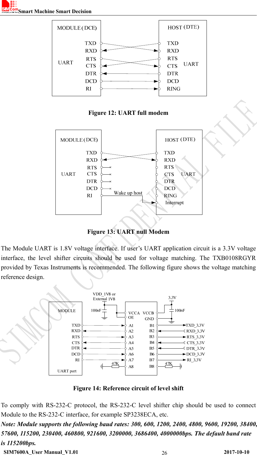
![Smart Machine Smart Decision SIM7600A_User Manual_V1.01 2017-10-10 273.3.2 RI and DTR Behavior The RI pin can be used to interrupt output signal to inform the host controller such as application CPU. Normally RI will stay at high level until certain conditions such as receiving SMS, or a URC report come in. It will then change to low level. It will stay low until the host controller clears the interrupted event with “AT+CRIRS” AT command. Figure 15: RI behaviour(SMS and URC report) Normally RI will be kept high until a voice call, then it will output periodic rectangular wave with 5900ms low level and 100ms high level. It will output this kind of periodic rectangular wave until the call is answered or hung up. Figure 16: RI behaviour(voice call) Note: For more details of AT commands about UART, please refer to document [1] and [22]. DTR pin can be used to wake Module from sleep. When Module enters sleep mode, pulling down DTR can wake Module. 3.4 USB Interface The Module contains a USB interface compliant with the USB2.0 specification as a peripheral, but the USB charging function is not supported.](https://usermanual.wiki/Simcom/201709.SIM7600A-User-Manual-V1-01-20171010/User-Guide-3598133-Page-27.png)
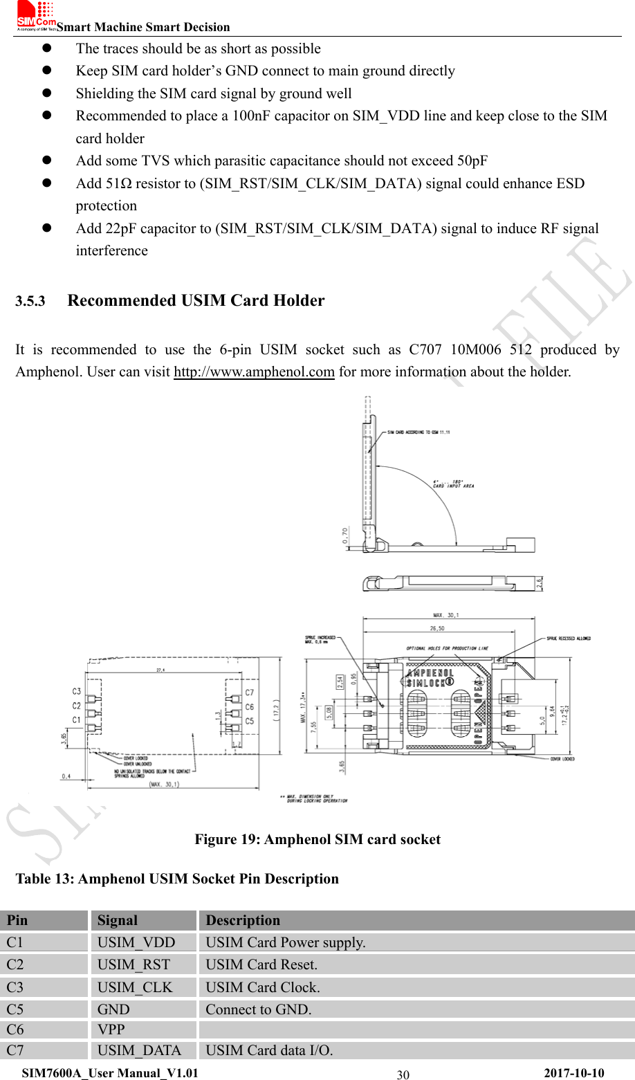
![Smart Machine Smart Decision SIM7600A_User Manual_V1.01 2017-10-10 29 Table 12: USIM Electronic characteristic 3.0V mode (USIM_VDD=2.95V) Symbol Parameter Min. Typ. Max. Unit USIM_VDD LDO power output voltage 2.75 2.95 3.05 V VIH High-level input voltage 0.65*USIM_VDD - USIM_VDD +0.3 V VIL Low-level input voltage -0.3 0 0.25*USIM_VDD V VOH High-level output voltage USIM_VDD -0.45 - USIM_VDD V VOL Low-level output voltage 0 0 0.45 V 3.5.1 USIM Application Guide It is recommended to use an ESD protection component such as ESDA6V1W5 produced by ST (www.st.com ) or SMF15C produced by ON SEMI (www.onsemi.com ). Note that the USIM peripheral circuit should be close to the USIM card socket.The following figure shows the 6-pin SIM card holder reference circuit. Figure 18: USIM interface reference circuit Note: USIM_DATA has been pulled up with a100KΩ resistor to USIM_VDD in module. A 100nF capacitor on USIM_VDD is used to reduceinterference. For more details of AT commands about USIM, please refer to document [1]. 3.5.2 SIM Card Design Guide SIM card signal could be interferenced by some high frequency signal, it is strongly recommended to follow these guidelines while designing: SIM card holder should be far away from antenna SIM traces should keep away from RF lines, VBAT and high-speed signal lines](https://usermanual.wiki/Simcom/201709.SIM7600A-User-Manual-V1-01-20171010/User-Guide-3598133-Page-29.png)
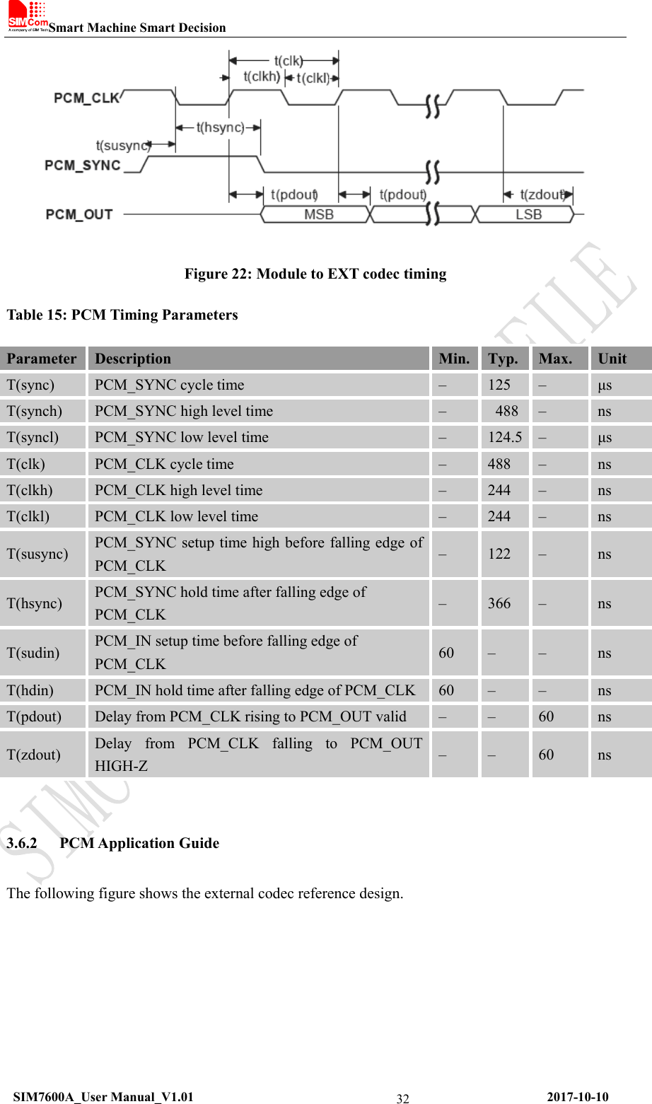
![Smart Machine Smart Decision SIM7600A_User Manual_V1.01 2017-10-10 313.6 PCM Interface Module provides a PCM interface for external codec, which can be used inmaster mode with short sync and 16 bits linear format. Table 14: PCM Format Note: For more details about PCM AT commands, please refer to document [1]. 3.6.1 PCM Timing Module supports 2.048 MHz PCM data and sync timing for 16 bits linear format codec. Figure 20: PCM_SYNC timing Figure 21: EXT codec to module timing Characteristics Specification LineInterfaceFormat Linear(Fixed) Datalength 16bits(Fixed) PCM Clock/Sync Source Master Mode(Fixed) PCMClockRate 2048 KHz (Fixed) PCMSyncFormat Shortsync(Fixed) Data Ordering MSB](https://usermanual.wiki/Simcom/201709.SIM7600A-User-Manual-V1-01-20171010/User-Guide-3598133-Page-31.png)
![Smart Machine Smart Decision SIM7600A_User Manual_V1.01 2017-10-10 33 Figure 23: Audio codec reference circuit Note: Module can transmit PCM data by theUSB portbesidesthe PCM interface. For more details please refer to documents [1] and [23]. 3.7 I2C Interface Module provides a I2C interface compatible with I2C specification, version 2.1, with clock rate up to 400 kbps. Its operation voltage is 1.8V. 3.7.1 I2C Design Guide The following figure shows the I2C bus reference design. Figure 24: I2C reference circuit Note: SDA and SCLhave pull-up resistors in module. So, 2 external pull up resistors are not needed in application circuit. “AT+CRIIC and AT+CWIIC” AT commands could be used to read/write register values of the I2C peripheral devices.For more details about AT commands please refer to document [1].](https://usermanual.wiki/Simcom/201709.SIM7600A-User-Manual-V1-01-20171010/User-Guide-3598133-Page-33.png)
![Smart Machine Smart Decision SIM7600A_User Manual_V1.01 2017-10-10 35Table 18: Pin multiplex function list Note:For more details of AT commands about GPIO multiplex function,please refer to document [1]. 3.11 Other interface 3.11.1 Sink Current Source The ISINK pin is VBATtolerant and intended to drive some passive devices such as LCD backlight, white LED, etc. Its output current can be up to 40 mA and be set by the AT command “AT+ CLEDITST”. Table 19: Sink current electronic characteristic Symbol Description Min. Typ. Max. Unit VISINK Voltage tolerant 0.5 - VBAT V IISINK Current tolerant 0 - 40 mA ISINK is a ground-referenced current sink. The following figure shows its reference circuit. Figure 26: ISINK reference circuit Pin Number Pin Name Default Function Alternate Function 4 SCL SCL GPIO11 5 SDA SDA GPIO10 12 USIM_DET GPIO34 USIM_DET 18 PCM_CLK PCM_CLK GPIO23,SPI_CLK I2C_SCL 19 PCM_SYNC PCM_SYNC GPIO20,SPI_MOSI 20 PCM_IN PCM_IN, GPIO21,SPI_MISO 21 PCM_OUT PCM_OUT GPIO22,SPI_CS_N I2C_SDA](https://usermanual.wiki/Simcom/201709.SIM7600A-User-Manual-V1-01-20171010/User-Guide-3598133-Page-35.png)
![Smart Machine Smart Decision SIM7600A_User Manual_V1.01 2017-10-10 36Note: The sinking current can be adjusted to meet the design requirement through the AT command “AT+ CLEDITST =<0>, <value>”.The “value” ranges from 0 to 8, on behalf of the current from 0mA to 40mA by 5mA step. 3.11.2 ADC Module has 1 dedicated ADC pins named ADC. They are available fordigitizing analog signals such as battery voltage and so on. These electronic specifications are shown in the following table. Table 20: ADC Electronic Characteristics Characteristics Min. Typ. Max. Unit Resolution –15 – Bits Input Range 0.1 1.7 V Input serial resistance 1 – – MΩ Note: “AT+CADC” can be used to read the voltage of the ADC pins, for more details, please refer to document [1].](https://usermanual.wiki/Simcom/201709.SIM7600A-User-Manual-V1-01-20171010/User-Guide-3598133-Page-36.png)
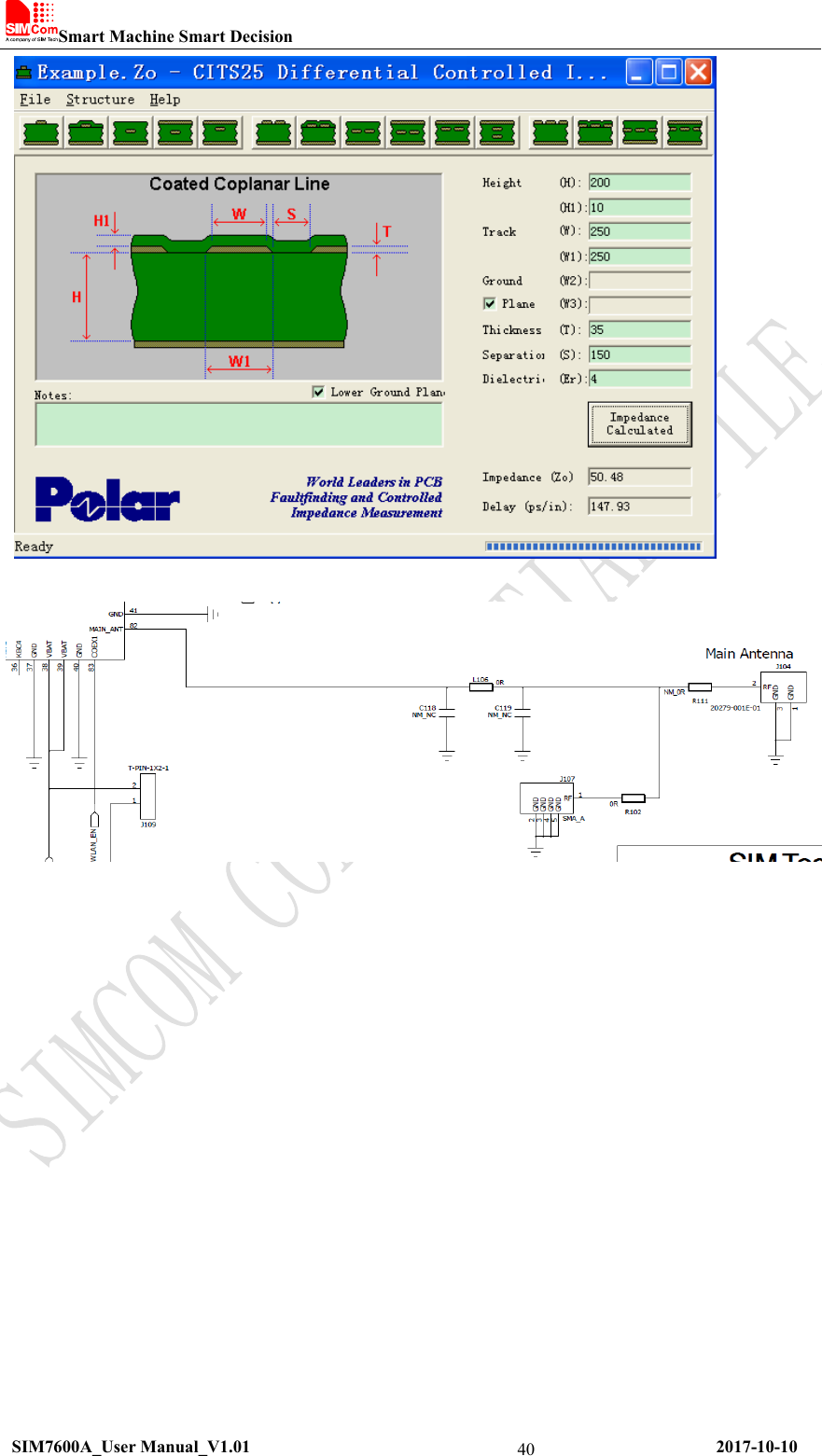
![Smart Machine Smart Decision SIM7600A_User Manual_V1.01 2017-10-10 39 Figure 28: Antenna matching circuit (DIV_ANT) In above figure, R3, C3, C4 and R4 are used for auxiliary antenna matching. By default, the R3, R4 are 0Ωresistors, and the C3, C4 are reserved for tuning. D2 is a TVS for ESD protection, and it is optional for users according to application environment. Two TVS are recommended in the table below. Table 26: Recommended TVS Package Part Number Vender 0201 LXES03AAA1-154 Murata 0402 LXES15AAA1-153 Murata Note:SIMCom suggests the LTE auxiliary antenna to be kept on, since there are many high bands in the designing of FDD-LTE. Because of the high insert loss of the RF cable and layout lines, the receiver sensitivity of these bands above will have risk to meet the authentication without the diversity antenna.For more details about auxiliary antenna design notice,please refer to document [25] To facilitate the antenna tuning and certification test, a RF connector and an antenna matching circuit should be added. The following figure is the recommended circuit. circuit should be added. The following figure is the recommended circuit.](https://usermanual.wiki/Simcom/201709.SIM7600A-User-Manual-V1-01-20171010/User-Guide-3598133-Page-39.png)
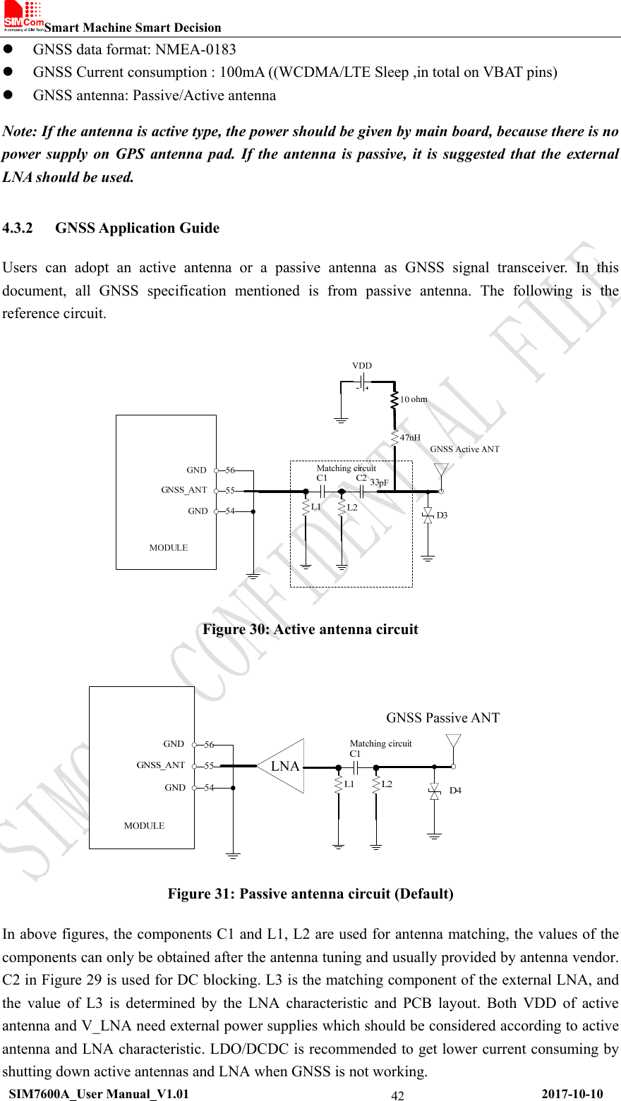
![Smart Machine Smart Decision SIM7600A_User Manual_V1.01 2017-10-10 43LNA should apply the following requirements as table 28. LNA is also suggested to put near the passive antenna. Table 27: LNA requirements Parameter Min Max Unit Vdd 1.5 3.3 V Idd 3 mA LNA_EN 1.3 V Gain 14 17 dB VSWR 2 GNSS can be used by NMEA port. User can select NMEA as output through UART or USB. NMEA sentences are automatic and no command is provided. NMEA sentences include GSV, GGA, RMC, GSA, and VTG. Before using GNSS, user should configure SIM7600A in proper operating mode by AT command. Please refer to related document for details. SIM7600A can also get position location information through AT directly. Note: GNSS is closed by default, it could be started by AT+CGPS. The AT command has two parameters, the first is on/off, and the second is GNSS mode. Default mode is standalone mode. AGPS mode needs more support from the mobile telecommunication network. Please refer to document [24] for more details.](https://usermanual.wiki/Simcom/201709.SIM7600A-User-Manual-V1-01-20171010/User-Guide-3598133-Page-43.png)
![Smart Machine Smart Decision SIM7600A_User Manual_V1.01 2017-10-10 46power supply. In this mode, the RF part of the module will not work but the serial port and USB port are still accessible. The power consumption in this mode is lower than normal mode. Power off Module will go into power off mode by sending the AT command “AT+CPOF” or by pulling down the PWRKEY pin normally. In this mode the power management unit shuts down the power supply and software is not active. The serial port and USB are is not accessible. 5.3.2 Sleep Mode In sleep mode, the current consumption of module will be reduced to the minimal level, and module can still receive paging message and SMS. Several hardware and software conditions must be satisfied together in order to let Module enter into sleep mode: 1. UART condition 2. USB condition 3. Software condition Note: Before designing, pay attention to how to realize sleeping/waking function and refer to Document [26] for more details. 5.3.3 Minimum Functionality Mode and Flight Mode Minimum functionality mode ceasesa majority functionof module, thus minimizing the power consumption. This mode is set by the AT command which provides a choice of the functionality levels. ● AT+CFUN=0: Minimum functionality ● AT+CFUN=1: Full functionality (Default) ● AT+CFUN=4: Flight mode If Module has been set to minimum functionality mode, the RF function and USIM card function will be closed. In this case, the serial port and USB are still accessible, but RF function and USIM card will be unavailable. If Module has been set to flight mode, the RF function will be closed. In this case, the serial port and USB are still accessible, but RF function will be unavailable. When Module is in minimum functionality or flight mode, it can return to full functionality by the AT command “AT+CFUN=1”. 5.4 Current Consumption The current consumption is listed in the table below.](https://usermanual.wiki/Simcom/201709.SIM7600A-User-Manual-V1-01-20171010/User-Guide-3598133-Page-46.png)
![Smart Machine Smart Decision SIM7600A_User Manual_V1.01 2017-10-10 486 SMT Production Guide 6.1 Top and Bottom View of Module Figure 32: Top and bottom view of Module 6.2 Typical SMT Reflow Profile SIMCom provides a typical soldering profile. Therefore the soldering profile shown below is only a generic recommendation and should be adjusted to the specific application and manufacturing constraints. Figure 33: The ramp-soak-spike Reflow Profile of Module Note: For more details about secondary SMT, please refer to the document [21].](https://usermanual.wiki/Simcom/201709.SIM7600A-User-Manual-V1-01-20171010/User-Guide-3598133-Page-48.png)
![Smart Machine Smart Decision SIM7600A_User Manual_V1.01 2017-10-10 55C. Related Documents Table 40: Related documents SN Title Description [1] SIM7X00 Series_AT Command Manual_V1.xx SIM7X00 Series_AT Command Manual [2] ITU-T Draft new recommendationV.25ter Serial asynchronous automatic dialing and control [3] GSM 07.07 Digital cellular telecommunications (Phase 2+); AT command set for GSM Mobile Equipment (ME) [4] GSM 07.10 Support GSM 07.10 multiplexing protocol [5] GSM 07.05 Digital cellular telecommunications (Phase 2+); Use of Data Terminal Equipment – Data Circuit terminating Equipment (DTE – DCE) interface for Short Message Service (SMS) and Cell Broadcast Service (CBS) [6] GSM 11.14 Digital cellular telecommunications system (Phase 2+); Specification of the SIM Application Toolkit for the Subscriber Identity Module – Mobile Equipment (SIM – ME) interface [7] GSM 11.11 Digital cellular telecommunications system (Phase 2+); Specification of the Subscriber Identity Module – Mobile Equipment (SIM – ME) interface [8] GSM 03.38 Digital cellular telecommunications system (Phase 2+); Alphabets and language-specific information [9] GSM 11.10 Digital cellular telecommunications system (Phase 2) ;Mobile Station (MS) conformance specification; Part 1: Conformance specification [10] 3GPP TS 51.010-1 Digital cellular telecommunications system (Release 5); Mobile Station (MS) conformance specification [11] 3GPP TS 34.124 Electromagnetic Compatibility (EMC) for mobile terminals and ancillary equipment. [12] 3GPP TS 34.121 Electromagnetic Compatibility (EMC) for mobile terminals and ancillary equipment. [13] 3GPP TS 34.123-1 Technical Specification Group Radio Access Network; Terminal conformance specification; Radio transmission and reception (FDD) [14] 3GPP TS 34.123-3 User Equipment (UE) conformance specification; Part 3: Abstract Test Suites. [15] EN 301 908-02 V2.2.1 Electromagnetic compatibility and Radio spectrum Matters (ERM); Base Stations (BS) and User Equipment (UE) for IMT-2000. Third Generation cellular networks; Part 2: Harmonized EN for IMT-2000, CDMA Direct Spread (UTRA FDD) (UE) covering essential requirements of article 3.2 of the R&TTE Directive [16] EN 301 489-24 V1.2.1 Electromagnetic compatibility and Radio Spectrum Matters (ERM); Electromagnetic Compatibility (EMC) standard for radio equipment and services; Part 24: Specific conditions for IMT-2000 CDMA Direct Spread (UTRA) for Mobile and portable (UE) radio and ancillary equipment [17] IEC/EN60950-1(2001) Safety of information technology equipment (2000) [18] 3GPP TS 51.010-1 Digital cellular telecommunications system (Release 5); Mobile Station (MS) conformance specification](https://usermanual.wiki/Simcom/201709.SIM7600A-User-Manual-V1-01-20171010/User-Guide-3598133-Page-55.png)
![Smart Machine Smart Decision SIM7600A_User Manual_V1.01 2017-10-10 56[19] GCF-CC V3.23.1 Global Certification Forum - Certification Criteria [20] 2002/95/EC Directive of the European Parliament and of the Council of 27 January 2003 on the restriction of the use of certain hazardous substances in electrical and electronic equipment (RoHS) [21] Module secondary-SMT-UGD-V1.xx Module secondary SMT Guidelines [22] SIM7X00 Series_UART_Application Note_V1.xx SIM7X00 Series_UART_Application Note [23] SIM7X00 Series_USB AUDIO_Application Note_V1.xx SIM7X00 Series_USB AUDIO_Application Note [24] Antenna design guidelines for diversity receiver system Antenna design guidelines for diversity receiver system [25] SIM7X00 Series_Sleep Mode_ Application Note_V1.xx SIM7X00 Series_Sleep Mode_ Application Note](https://usermanual.wiki/Simcom/201709.SIM7600A-User-Manual-V1-01-20171010/User-Guide-3598133-Page-56.png)