Simcom 201709 LTE-FDD/HSPA MODULE User Manual SIM7600A User Manual V1 01 20171010
Shanghai Simcom Ltd. LTE-FDD/HSPA MODULE SIM7600A User Manual V1 01 20171010
Simcom >
Contents
- 1. SIM7600A_User_Manual_V1.01_20171010
- 2. User Manual
SIM7600A_User_Manual_V1.01_20171010
SIM7600A_User Manual_V1.01

Smart Machine Smart Decision
SIM7600A_User Manual_V1.01 2017-10-10
2
Compliance Information:
FCC Compliance Statement: This device complies with Part 15 of the FCC Rules . Operation is
subject to the following two conditions: 1. This device may not cause harmful interference, and 2.
This device must accept any interference received, including interference that may cause undesired
operation. This device must accept any interference received, including interference that may cause
undesired operation. Product that is a radio transmitter is labeled with FCC ID.
FCC Caution:
(1)Exposure to Radio Frequency Radiation. This equipment must be installed and operated in
accordance with provided instructions and the antenna(s) used for this transmitter must be installed
to provide a separation distance of at least 20 cm from all persons and must not be collocated or
operating in conjunction with any other antenna or transmitter. End-users and installers must be
provided with antenna installation instructions and transmitter operating conditions for satisfying RF
exposure compliance.
(2)Any changes or modifications not expressly approved by the grantee of this device could void the
user's authority to operate the equipment.
(3)This Transmitter must not be co-located or operating in conjunction with any other antenna or
transmitter.
(4)Changes or modifications to this unit not expressly approved by the party responsible for
compliance could void the user authority to operate the equipment.
(5) the modules FCC ID is not visible when installed in the host, or (6) if the host is marketed so that
end users do not have straight forward commonly used methods for access to remove the module so
that the FCC ID of the module is visible; then an additional permanent label referring to the enclosed
module: Contains Transmitter Module FCC ID: UDV-201709 or Contains FCC ID: UDV-201709

Smart Machine Smart Decision
SIM7600A_User Manual_V1.01 2017-10-10
3
Document Title SIM7600A_User Manual
Version V1.01
Date 2017-10-10
Status Released
Document Control ID SIM7600A_User Manual_V1.01
General Notes
SIMCom offers this information as a service to its customers to support the application and
engineering efforts that use the products designed by SIMCom. The information provided is based
on the requirements specifically from the customers. SIMCom has not undertaken any independent
search for additional relevant information, including any information that may be in the customer’s
possession. Furthermore, the system validation of the product designed by SIMCom within a larger
electronic system remains the responsibility of the customer or the customer’s system integrator.
All specifications supplied herein are subject to change without notice.
Copyright
This document contains the proprietary technical information which is the property of SIMCom
Limited, copying of this document, giving it to others, the using or communication of the contents
thereof are forbidden without the official authority by SIMCom. Offenders are liable to the
payment of the damages. All rights are reserved in the event of grant of a patent or the registration
of a utility model or design. All specifications supplied herein are subject to change without notice
Copyright © SIMCom Wireless Solutions Co., Ltd. 2017

Smart Machine Smart Decision
SIM7600A_User Manual_V1.01 2017-10-10
4
Contents
Contents ............................................................................................................................................. 4
Table Index ........................................................................................................................................ 6
Figure Index ...................................................................................................................................... 7
Revision History ................................................................................................................................ 8
1Introduction ................................................................................................................................ 9
1.1Product Outline ..................................................................................................................... 9
1.2Hardware Interface Overview ............................................................................................... 9
1.3Hardware Block Diagram...................................................................................................... 9
1.4Functional Overview ........................................................................................................... 10
2Package Information ............................................................................................................... 12
2.1Pin Assignment Overview ................................................................................................... 12
2.2Pin Description .................................................................................................................... 14
2.3Mechanical Information ...................................................................................................... 18
2.4Footprint Recommendation ................................................................................................. 19
3Interface Application ............................................................................................................... 20
3.1Power Supply ...................................................................................................................... 20
3.1.1Power supply Design Guide ......................................................................................... 20
3.1.2Recommended Power Supply Circuit .......................................................................... 21
3.1.3Voltage Monitor ............................................................................................................ 22
3.2Power on/Power off/Reset Function .................................................................................... 22
3.2.1Power on ....................................................................................................................... 22
3.2.2Power off ...................................................................................................................... 23
3.2.3Reset Function .............................................................................................................. 24
3.3UART Interface ................................................................................................................... 25
3.3.1UART Design Guide .................................................................................................... 25
3.3.2RI and DTR Behavior ................................................................................................... 27
3.4USB Interface ...................................................................................................................... 27
3.4.1USB Application Guide ................................................................................................ 28
3.5USIM Interface.................................................................................................................... 28
3.5.1USIM Application Guide .............................................................................................. 29
3.5.2SIM Card Design Guide ............................................................................................... 29
3.5.3Recommended USIM Card Holder .............................................................................. 30
3.6PCM Interface ..................................................................................................................... 31
3.6.1PCM Timing ................................................................................................................. 31
3.6.2PCM Application Guide ............................................................................................... 32
3.7I2C Interface ....................................................................................................................... 33
3.7.1I2C Design Guide ......................................................................................................... 33
3.8Network Status .................................................................................................................... 34
3.9Operating Status Indication ................................................................................................. 34
3.10Pin Multiplex Function .................................................................................................... 34

Smart Machine Smart Decision
SIM7600A_User Manual_V1.01 2017-10-10
5
3.11Other interface ................................................................................................................. 35
3.11.1Sink Current Source .................................................................................................. 35
3.11.2ADC .......................................................................................................................... 36
4RF Specifications ...................................................................................................................... 37
4.1WCDMA/LTE RF Specifications ....................................................................................... 37
4.2WCDMA/LTE Antenna Design Guide ................................................................................ 38
4.3GNSS .................................................................................................................................. 41
4.3.1GNSS Technical specification ...................................................................................... 41
4.3.2GNSS Application Guide ............................................................................................. 42
5Electrical Specifications ........................................................................................................... 44
5.1Absolute Maximum Ratings................................................................................................ 44
5.2Operating Conditions .......................................................................................................... 44
5.3Operating Mode .................................................................................................................. 45
5.3.1Operating Mode Definition .......................................................................................... 45
5.3.2Sleep Mode ................................................................................................................... 46
5.3.3Minimum Functionality Mode and Flight Mode .......................................................... 46
5.4Current Consumption .......................................................................................................... 46
5.5ESD Notes ........................................................................................................................... 47
6SMT Production Guide ........................................................................................................... 48
6.1Top and Bottom View of Module ........................................................................................ 48
6.2Typical SMT Reflow Profile ............................................................................................... 48
6.3Moisture Sensitivity Level (MSL) ...................................................................................... 49
6.4Stencil Foil Design Recommendation ................................................................................. 49
7Packaging .................................................................................................................................. 50
Appendix .......................................................................................................................................... 52
A. Reference Design ...................................................................................................................... 52
B. Coding Schemes and Maximum Net Data Rates over Air Interface......................................... 53
C. Related Documents ................................................................................................................... 55
D. Terms and Abbreviations .......................................................................................................... 57
E. Safety Caution ........................................................................................................................... 59

Smart Machine Smart Decision
SIM7600A_User Manual_V1.01 2017-10-10
6
Table Index
Table 1: SIM7600A frequency bands ................................................................................................................... 9
Table 2: General features ................................................................................................................................... 10
Table 3: Pin Definitions ..................................................................................................................................... 13
Table 4: IO parameters definition....................................................................................................................... 14
Table 5: Pin description...................................................................................................................................... 14
Table 6: VBAT Pins electronic characteristic ..................................................................................................... 20
Table 7: Recommended zener diode list ............................................................................................................. 21
Table 8: Power on timing and electronic characteristic ...................................................................................... 23
Table 9: Power off timing and Electronic Characteristic .................................................................................... 24
Table 10: RESET pin electronic characteristic ................................................................................................... 25
Table 11: USIM Electronic characteristic in 1.8V mode (USIM_VDD=1.8V) .................................................. 28
Table 12: USIM Electronic characteristic 3.0V mode (USIM_VDD=2.95V) .................................................... 29
Table 13: Amphenol USIM Socket Pin Description ........................................................................................... 30
Table 14: PCM Format ....................................................................................................................................... 31
Table 15: PCM Timing Parameters .................................................................................................................... 32
Table 16: NETLIGHT pin status ........................................................................................................................ 34
Table 17: Pin definition of the STATUS ............................................................................................................ 34
Table 18: Pin multiplex function list .................................................................................................................. 35
Table 19: Sink current electronic characteristic ................................................................................................. 35
Table 20: ADC Electronic Characteristics .......................................................................................................... 36
Table 21: Conducted transmission power .......................................................................................................... 37
Table 22: Operating frequencies ........................................................................................................................ 37
Table 23: Conducted receive sensitivity ............................................................................................................. 37
Table 24: Reference sensitivity (QPSK) ............................................................................................................ 37
Table 25: Trace Loss .......................................................................................................................................... 38
Table 26: Recommended TVS ........................................................................................................................... 39
Table 27: LNA requirements .............................................................................................................................. 43
Table 28: Absolute maximum ratings ................................................................................................................. 44
Table 29: Recommended operating ratings ........................................................................................................ 44
Table 30: 1.8V Digital I/O characteristics* ........................................................................................................ 44
Table 31: Operating temperature ........................................................................................................................ 45
Table 32: Operating mode Definitions ............................................................................................................... 45
Table 33: Current consumption on VBAT Pins (VBAT=3.8V) .......................................................................... 47
Table 34: The ESD performance measurement table (Temperature: 25℃, Humidity: 45%) ............................. 47
Table 35: Moisture Sensitivity Level and Floor Life ......................................................................................... 49
Table 36: Tray size ............................................................................................................................................. 50
Table 37: Small Carton size ............................................................................................................................... 51
Table 38: Big carton size .................................................................................................................................... 51
Table 39: Coding schemes and maximum net data rates over air interface ........................................................ 53
Table 40: Related documents ............................................................................................................................. 55
Table 41: Terms and Abbreviations .................................................................................................................... 57
Table 42: Safety caution ..................................................................................................................................... 59

Smart Machine Smart Decision
SIM7600A_User Manual_V1.01 2017-10-10
7
Figure Index
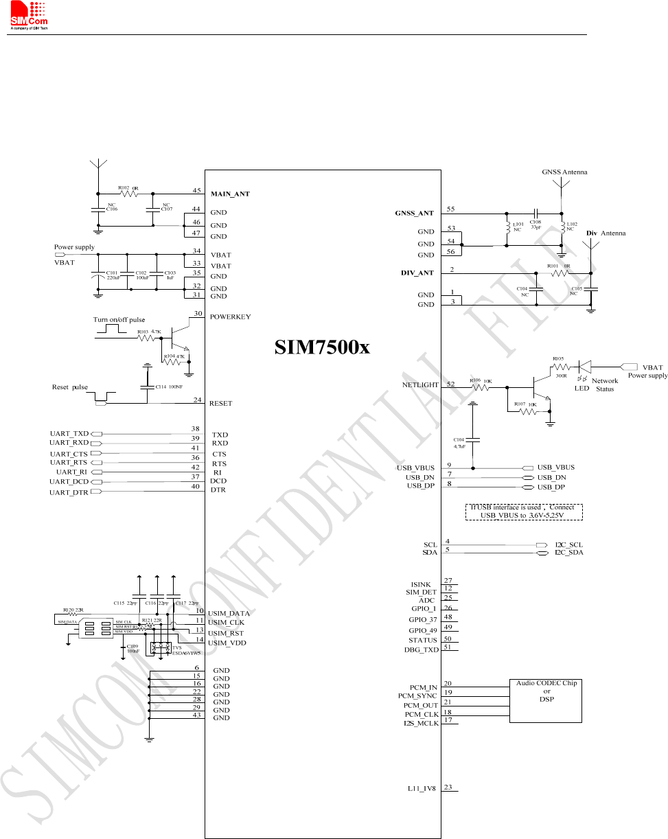
Figure 1: SIM7600A Block Diagram ................................................................................................................. 10
Figure 2: Pin assignment overview .................................................................................................................... 12
Figure 3: Dimensions (Unit: mm) ...................................................................................................................... 18
Figure 4: Footprint recommendation (Unit: mm) ............................................................................................... 19
Figure 5: Power supply application circuit......................................................................................................... 20
Figure 6: Linear regulator reference circuit ....................................................................................................... 21
Figure 7: Switching modepower supply reference circuit .................................................................................. 21
Figure 8: ReferencePower on/offCircuit ............................................................................................................ 22
Figure 9: Power on timing sequence .................................................................................................................. 23
Figure 10: Power off timing sequence ............................................................................................................... 24
Figure 11: Reference reset circuit ...................................................................................................................... 25
Figure 12: UART full modem ............................................................................................................................ 26
Figure 13: UART null Modem ........................................................................................................................... 26
Figure 14: Reference circuit of level shift .......................................................................................................... 26
Figure 15: RI behaviour(SMS and URC report) ........................................................................................... 27
Figure 16: RI behaviour(voice call) .............................................................................................................. 27
Figure 17: USB reference circuit ....................................................................................................................... 28
Figure 18: USIM interface reference circuit ...................................................................................................... 29
Figure 19: Amphenol SIM card socket .............................................................................................................. 30
Figure 20: PCM_SYNC timing .......................................................................................................................... 31
Figure 21: EXT codec to module timing ............................................................................................................ 31
Figure 22: Module to EXT codec timing ........................................................................................................... 32
Figure 23: Audio codec reference circuit ........................................................................................................... 33
Figure 24: I2C reference circuit ......................................................................................................................... 33
Figure 25: NETLIGHT reference circuit ............................................................................................................ 34
Figure 26: ISINK reference circuit .................................................................................................................... 35
Figure 27: Antenna matching circuit (MAIN_ANT) .......................................................................................... 38
Figure 28: Antenna matching circuit (DIV_ANT) ............................................................................................. 39
Figure 29: Antenna matching circuit (MAIN_ANT) .......................................................................................... 41
Figure 30: Active antenna circuit ....................................................................................................................... 42
Figure 31: Passive antenna circuit (Default) ...................................................................................................... 42
Figure 32: Top and bottom view of Module ....................................................................................................... 48
Figure 33: The ramp-soak-spike Reflow Profile of Module............................................................................... 48
Figure 34: Packaging introduce ......................................................................................................................... 50
Figure 34: Module tray drawing introduce......................................................................................................... 50
Figure 36: Small carton drawing introduce ........................................................................................................ 51
Figure 37: Big carton drawing introduce ........................................................................................................... 51
Figure 38: Reference design .............................................................................................................................. 52

Smart Machine Smart Decision
SIM7600A_User Manual_V1.01 2017-10-10
8
Revision History
Data Version Description of change Author
2016-09-30 V1.00 new Shengwu.sun
Smart Machine Smart Decision
SIM7600A_User Manual_V1.01 2017-10-10
9
1 Introduction
This document describes the electronic specifications, RF specifications, interfaces, mechanical
characteristics and testing results of the SIMCom SIM7600A. With the help of this document and
other software application notes/user guides, users can understand and use modules to design and
develop applications quickly.
1.1 Product Outline
The SIM7600A support many air-interface standards, refer to the following table.
Table 1: SIM7600A frequency bands
Standard Frequency SIM7600A
WCDMA BAND2
BAND5
LTE
LTE-FDD B2
LTE-FDD B4
LTE-FDD B12
With a smallphysical dimension of 30*30*2.9 mm and with the functionsintegrated, the Module
can meet almost any space requirement in users’ applications, such as smart phones, PDA’s,
industrial handhelds, machine-to-machine, vehicle applications, etc.
1.2 Hardware Interface Overview
The interfaces that are described in detail in the next chapters include:
● Power Supply
● USB Interface
● UART Interface
● USIM Interface
● GPIO
● ADC
● Power Output
● Current Sink Source
● PCM Interface
● I2C Interface
1.3 Hardware Block Diagram
The block diagram of the Module is shown in the figure below.
Smart Machine Smart Decision
SIM7600A_User Manual_V1.01 2017-10-10
10
GSM/WCDMA
/LTE
RF FEM
GSM/
WCDMA/LTE PA
RF
Transceiver
Baseband
XO
19.2MHz
NAND
Flash
I2C
PCM
Interrupt
Status LED
USB
USIM
Power On
Reset
UART
GPIOs
ADC
LDO
VBAT
Sink Current Source
DDR
Main Antenna
Power
Management
Qualcomm
Chip
SMT Interface
WCDMA
/LTE
RF FEM
AUX Antenna
SYSTEM POWER
VBAT
GNSS RF
GNSS Antenna
Figure 1: SIM7600A Block Diagram
1.4 Functional Overview
Table 2: General features
Feature Implementation
Power supply Single supply voltage 3.4~4.2V
Power saving Current in sleep mode : <5mA
Radio frequency bands Please refer to the table 1
Transmitting power WCDMA: Class 3 (0.25W)
LTE: Class 3 (0.25W)
Data Transmission
Throughout
HSPA+: 5.76 Mbps(UL), 42 Mbps(DL)
LTE Category 1: 10 Mbps (DL)
LTE Category 1: 5 Mbps (UL)
Antenna WCDMA /LTE main antenna
WCDMA /LTE auxiliary antenna
SMS
MT, MO, CB, Text and PDU mode
SMS storage: USIM card or ME(default)
Transmission of SMS alternatively over CS or PS.
USIM interface Support identity card: 1.8V/ 3V
USIM application toolkit Support SAT class 3, GSM 11.14 Release 98
Support USAT
Phonebook management Support phonebook types: DC,MC,RC,SM,ME,FD,ON,LD,EN
Smart Machine Smart Decision
SIM7600A_User Manual_V1.01 2017-10-10
11
Audio feature
Support PCM interface
Only support PCM master mode and short frame sync, 16-bit linear data
formats
UART interface
A full modem serial port by default
Baud rate: 300bps to 4Mbps(default:115200bps)
Auto-bauding baud rate: 9600,19200,38400,57600,115200bps
Can be used as the AT commands or data stream channel.
Support RTS/CTS hardware handshake
Multiplex ability according to GSM 07.10 Multiplexer Protocol.
USB USB 2.0 specification-compliant as a peripheral
Firmware upgrade USB Firmware upgrade over USB interface
USB 2.0 specification-compliant as a peripheral
Physical characteristics Weight:5.5g
Size:30*30*2.9mm
Temperature range
Normal operation temperature: -30°C to +80°C
Extended operation temperature: -40°C to +85°C*
Storage temperature -45°C to +90°C
*Note: Module is able to make and receive voice calls, data calls, SMS and make
WCDMA/HSPA+/LTE traffic in -40℃ ~ +85℃. The performance will be reduced slightly from
the 3GPP specifications if the temperature is outside the normal operating temperature range
and still within the extreme operating temperature range.
Smart Machine Smart Decision
SIM7600A_User Manual_V1.01 2017-10-10
12
2 Package Information
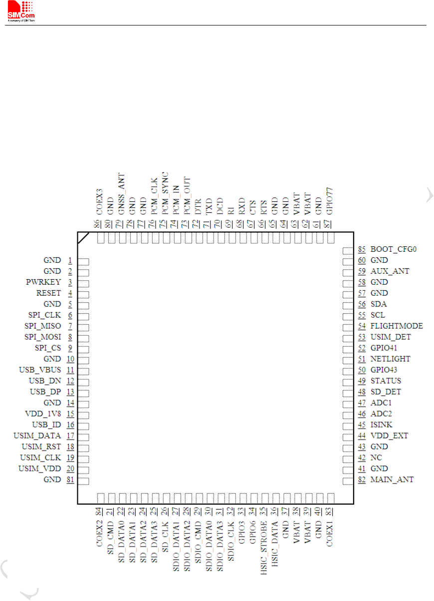
2.1 Pin Assignment Overview
All functions of the SIM7600A will be provided through 56 pads that will be connected to the
customers’ platform. The following Figure is a high-level view of the pin assignment of the
SIM7600A.
Figure 2: Pin assignment overview
SIM7600A
(Top View)
Smart Machine Smart Decision
SIM7600A_User Manual_V1.01 2017-10-10
13
Table 3: Pin Definitions
Pin No. Pin name Pin No. Pin name
1 GND 2 GND
3 PWRKEY 4 RESET
5 GND 6 SPI_CLK
7 SPI_MISO 8 SPI_MOSI
9 SPI_CS 10 GND
11 USB_VBUS 12 USB_DN
13 USB_DP 14 GND
15 VDD_1V8 16 USB_ID
17 USIM_DATA 18 USIM_RST
19 USIM_CLK 20 USIM_VDD
21 SD_CMD 22 SD_DATA0
23 SD_DATA1 24 SD_DATA2
25 SD_DATA3 26 SD_CLK
27 SDIO_DATA1 28 SDIO_DATA2
29 SDIO_CMD 30 SDIO_DATA0
31 SDIO_DATA3 32 SDIO_CLK
33 GPIO3 34 GPIO6
35 HSIC_STROBE 36 HSIC_DATA
37 GND 38 VBAT
39 VBAT 40 GND
41 GND 42 NC (RESERVED)
43 GND 44 VDD_EXT
45 ISINK 46 ADC2
47 ADC1 48 SD_DET
49 STATUS 50 GPIO43*
51 NETLIGHT 52 GPIO41
53 USIM_DET 54 FLIGHTMODE
55 SCL 56 SDA
57 GND 58 GND
59 AUX_ANT 60 GND
61 GND 62 VBAT
63 VBAT 64 GND
65 GND 66 RTS
67 CTS 68 RXD
Smart Machine Smart Decision
SIM7600A_User Manual_V1.01 2017-10-10
14
69 RI 70 DCD
71 TXD 72 DTR
73 PCM_OUT 74 PCM_IN
75 PCM_SYNC 76 PCM_CLK
77 GND 78 GND
79 GNSS_ANT 80 GND
81 GND 82 MAIN_ANT
83 COEX1* 84 COEX2
85 BOOT_CFG0* 86 COEX3*
87 GPIO77
*Note: Before the normal power up, pin48 cannot be pulled up.
2.2 Pin Description
Table 4: IO parameters definition
Pin type Description
PI Power input
PO Power output
AI Analog input
AIO Analog input/output
I/O Bidirectional input /output
DI Digital input
DO Digital output
DOH Digital output with high level
DOL Digital output with low level
PU Pull up
PD Pull down
Table 5: Pin description
Pin name Pin No. Default
status Description Comment
Power supply
VBAT 38,39,
62,63 PI Power supply, voltage range:
3.4~4.2V.
VDD_EXT 44 PO
LDO power output for other
external circuits with Max
150mA current output. Its
output voltage is 0V by default.
If unused, keep it
open.

Smart Machine Smart Decision
SIM7600A_User Manual_V1.01 2017-10-10
15
(The voltage can be
configured to 2.8V by AT
command).
VDD_1V8 15 PO
1.8V SMPS output with Max
50mA current output for
external circuit, such as level
shift circuit.
If unused, keep it
open.
GND
1,2,5,
10,14,37
,40,41,4
3,57,58,
60,61,64
,65,77,7
8,80,81
Ground
System Control
PWRKEY 3 DI,PU System power on/off control
input, active low.
The high voltage is
0.8V;
RESET 4 DI, PU System reset control input,
active low.
RESET has been
pulled up to 1.8V via
40Kohm resistor
internally.
SD interface
SD_CMD 21 DO SDIO command
If unused, keep them
open.
SD_DATA0 22 I/O
SDIO data
SD_DATA1 23 I/O
SD_DATA2 24 I/O
SD_DATA3 25 I/O
SD_CLK 26 DO SDIO clock
USIM interface
USIM_DATA 17 I/O,PU
USIM Card data I/O, which has
been pulled up via a 100KR
resistor to USIM_VDD
internally. Do not pull it up or
down externally.
All lines of USIM
interface should be
protected against
ESD.
USIM_RST 18 DO USIM Reset
USIM_CLK 19 DO USIM clock
USIM_VDD 20 PO
Power output for USIM card,
its output Voltage depends on
USIM card type automatically.
Its output current is up to
50mA.
SPI interface
SPI_CLK 6 DO SPI clock output Only support SPI
master mode.
SPI_MISO 7 DI SPI master in/slave out data
Smart Machine Smart Decision
SIM7600A_User Manual_V1.01 2017-10-10
16
SPI_MOSI 8 DO SPI master out/slave in data If unused, please keep
them open.
SPI_CS 9 DO SPI chip-select output
USB
USB_VBUS 11 DI,PD Valid USB detection input with
3.0~5.25V detection voltage
USB_DN 12 I/O Negative line of the differential,
bi-directional USB signal.
USB_DP 13 I/O Positive line of the differential,
bi-directional USB signal.
USB_ID 16 DI High-speed USB ID input
K
ee
p
it o
p
en.
UART interface
RTS 66 DOH Request to send
If unused, keep them
open.
CTS 67 DI,PU Clear to Send
RXD 68 DI,PU Receive Data
RI 69 DOH Ring Indicator
DCD 70 DOH Carrier detects
TXD 71 DOH Transmit Data
DTR 72 DI,PU DTE get ready
I2C interface
SCL 55 DO I2C clock output If unused, keep open,
or else pull them up
via 4.7KΩ resistors to
1.8V.
SDA 56 I/O I2C data input/output
SDIO interface
SDIO_DATA1 27 I/O SDIO data1
For WLAN solution
SDIO_DATA2 28 I/O SDIO data2
SDIO_CMD 29 DO SDIO command
SDIO_DATA0 30 I/O SDIO data0
SDIO_DATA3 31 I/O SDIO data3
SDIO_CLK 32 DO SDIO clock
HSIC interface
HSIC_STROB
E 35 DO HSIC strobe wakeup Reserved
HSIC_DATA 36 I/O HSIC data
PCM interface
PCM_OUT 73 DO PCM data output.
If unused, please keep
them open.
PCM_IN 74 DI PCM data input.
PCM_SYNC 75 DO PCM data frame sync signal.
PCM_CLK 76 DO PCM data bit clock.
GPIO
NETLIGHT 51 DO LED control output as network
status indication.
If unused, keep them
open.

Smart Machine Smart Decision
SIM7600A_User Manual_V1.01 2017-10-10
17
FLIGHTMODE 54 DI,PU
Flight Mode control input.
High level(or open): Normal
Mode
Low level: Flight Mode
DO NOT PULL UP
GPIO43 DURING
NORMAL POWER
UP!
STATUS 49 DO
Operating status output.
High level: Power on and
firmware ready
Low level: Power off
GPIO41 52 IO GPIO
GPIO43 50 IO GPIO
GPIO3 33 IO GPIO
GPIO6 34 IO GPIO
SD_DET 48 IO
Default: GPIO
Optional: SD card detecting
input.
H: SD card is removed
L: SD card is inserted
USIM_DET 53 IO
Default: GPIO
Optional: USIM card detecting
input.
H: USIM is removed
L: USIM is inserted
GPIO77 87 IO GPIO
RF interface
MAIN _ANT 82 AIO MAIN antenna soldering pad
GNSS_ANT 79 AI GNSS antenna soldering pad
AUX_ANT 59 AI Auxiliary antenna soldering pad
Other interface
ISINK 45 PI Ground-referenced current sink.
If unused, please keep
them open.
ADC1 47 AI Analog-digital converter input
1
ADC2 46 AI Analog-digital converter input
2
COEX1 83 I/O
RF synchronizing between
Wi-Fi and LTE.
If unused, keep them
open.
DO NOT PULL UP
COEX1 AND COEX2
DURING NORMAL
POWER UP!
COEX2 84 I/O
COEX3 86 I/O
BOOT_CFG0 85 DI,PD
Boot configuration input.
Module will be forced into
USB download mode by
connect 85 pin to VDD_1V8
during power up.
Do place 2 test points
for debug.
DO NOT PULL UP
BOOT_CFG0
DURING NORMAL
POWER UP!
NC 42 No connection. Keep it open
Smart Machine Smart Decision
SIM7600A_User Manual_V1.01 2017-10-10
18
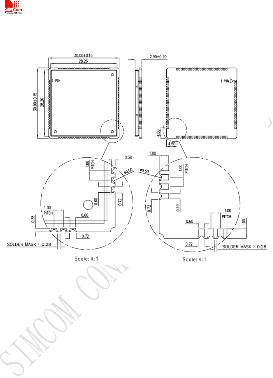
2.3 Mechanical Information
The following figure shows the package outline drawing of Module.
Figure 3: Dimensions (Unit: mm)
Smart Machine Smart Decision
SIM7600A_User Manual_V1.01 2017-10-10
19
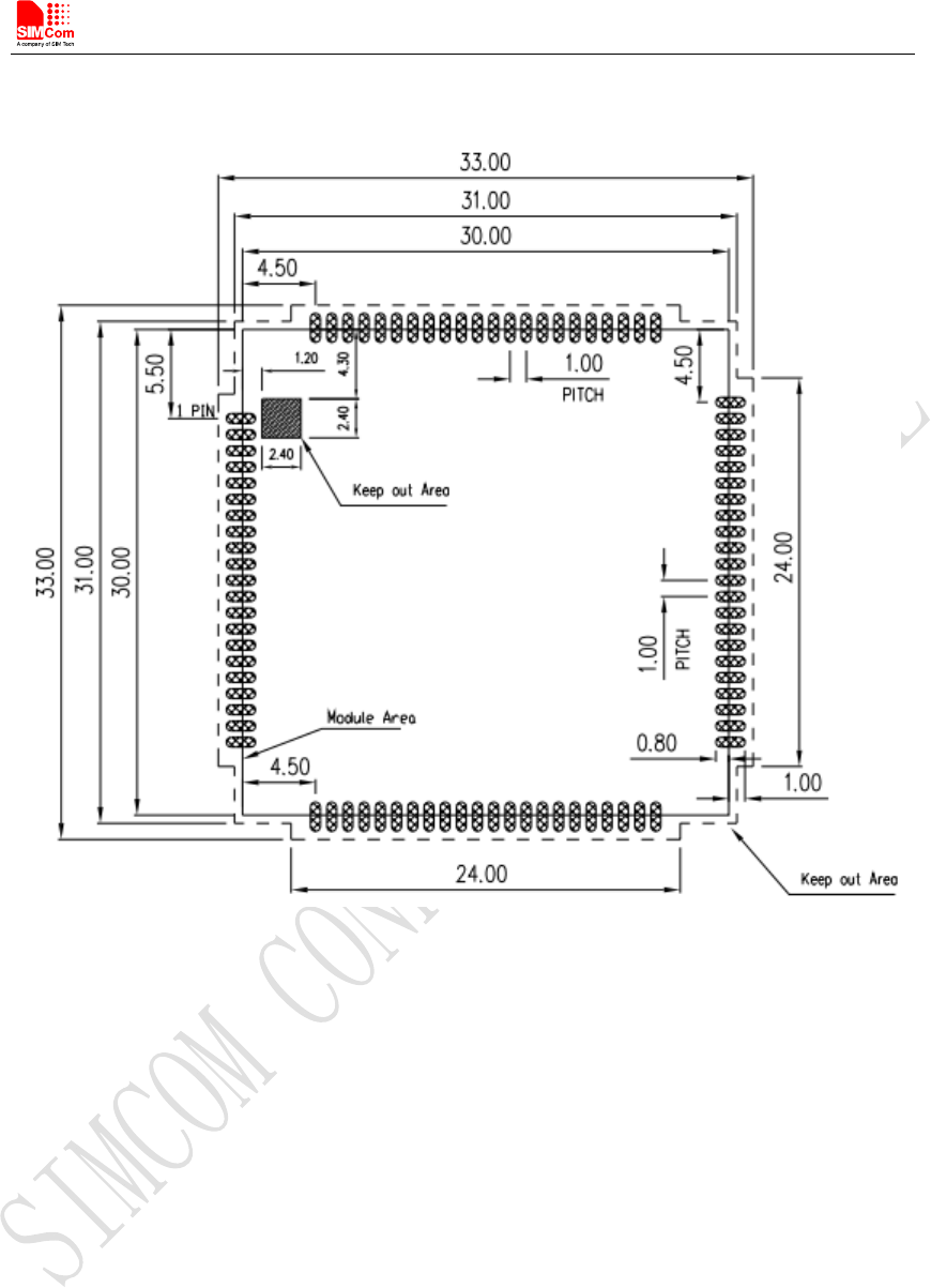
2.4 Footprint Recommendation
Figure 4: Footprint recommendation (Unit: mm)
Smart Machine Smart Decision
SIM7600A_User Manual_V1.01 2017-10-10
20
3 Interface Application
3.1 Power Supply
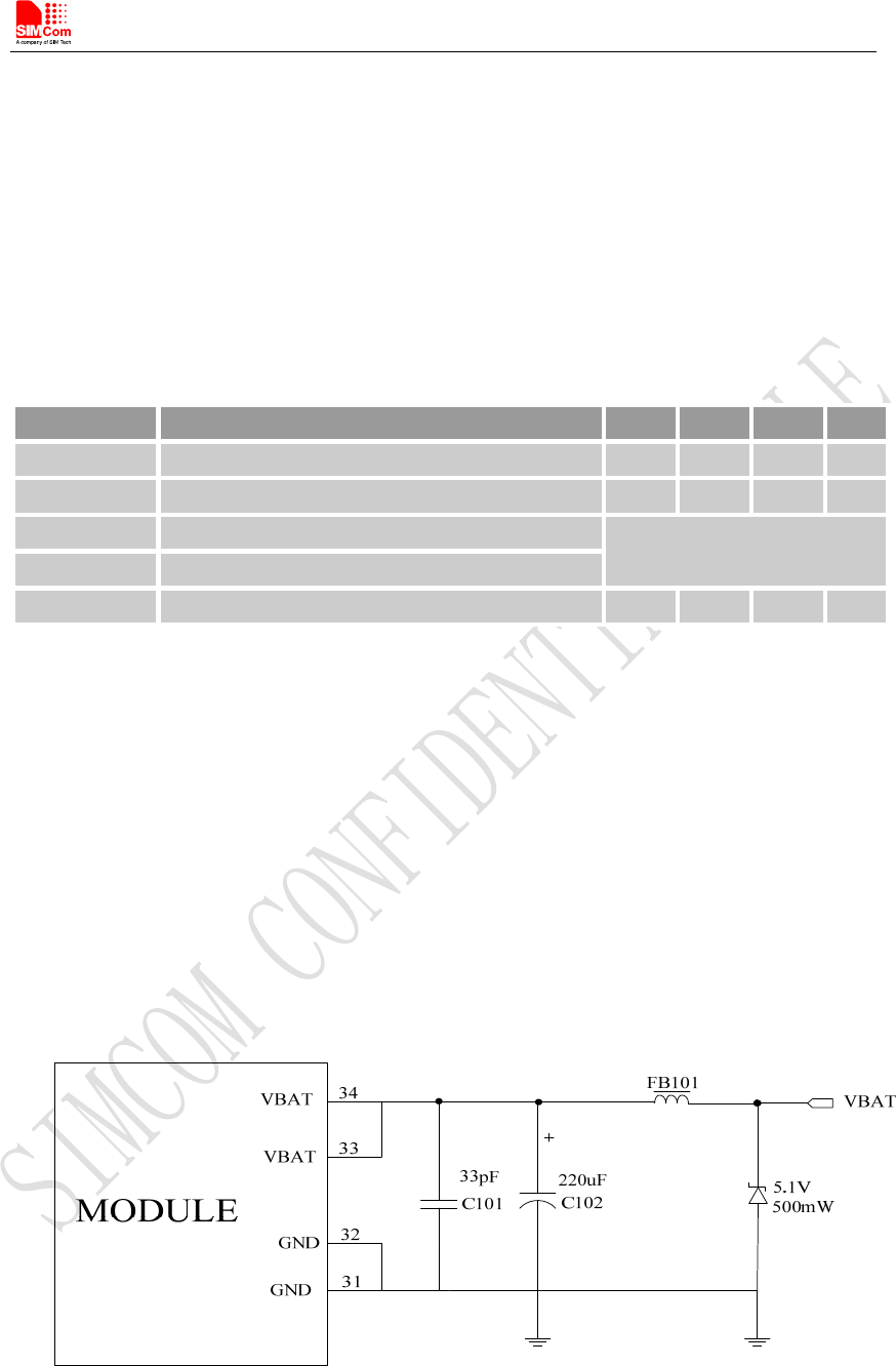
On VBAT pads, a ripple current up to 2A typically, may cause voltage drop. Therefore, the power
supply for these pads must be able to provide sufficient current up to more than 2A in order to
avoid the voltage drop of more than 300mV.
Table 6: VBAT Pins electronic characteristic
Symbol Description Min. Typ. Max. Unit
VBAT Module power voltage 3.4 3.8 4.2 V
IVBAT(peak) Module power peak current in normal mode. 1.0 - 2 A
IVBAT(average) Module power average current in normal mode Please refer to the table 34
IVBAT(sleep) Power supply current in sleep mode
IVBAT(power-off) Module power current in power off mode. - - 20 uA
3.1.1 Power supply Design Guide
Make sure that the voltage on the VBAT pins will never drop below 3.4V.
Note: If the power supply for BAT pins can support up to 2A, using a total of more than 220uF
capacitors is recommended, or else users must use a total of 1000uF capacitors, in order to avoid
the voltage drop of more than 300mV.
Some multi-layer ceramic chip (MLCC) capacitors (0.1/1uF) with low ESR in high frequency band
can be used for EMC.
These capacitors should be put as close as possible to VBAT pads. Also, user should keep VBAT
trace on the circuit board wider than 2 mm to minimize PCB trace impedance. The following figure
shows the recommended circuit.
Figure 5: Power supply application circuit
Smart Machine Smart Decision
SIM7600A_User Manual_V1.01 2017-10-10
21
In addition, in order to guard over voltage protection, it is suggested to use a zener diode with 5.1V
reverse zener voltage and more than 500mW power dissipation.
Table 7: Recommended zener diode list
No. Manufacturer Part Number power dissipation Package
1 On semi MMSZ5231BT1G 500mW SOD123
2 Prisemi PZ3D4V2H 500mW SOD323
3 Vishay MMSZ4689-V 500mW SOD123
4 Crownpo CDZ55C5V1SM 500mW 0805
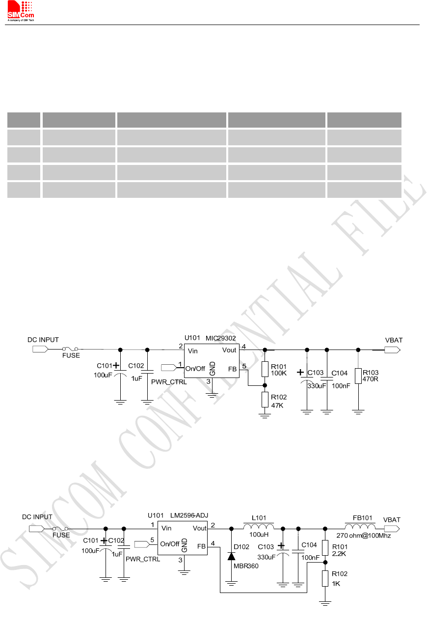
3.1.2 Recommended Power Supply Circuit
It is recommended that a switching modepower supply or linear regulator power supply is used. It
is important to make sure that all the components used in the power supply circuit can resist a peak
current up to 2A.
The following figure shows the linear regulatorreference circuit with 5V input and 3.8V output.
Figure 6: Linear regulator reference circuit
If there is a big voltage difference between input and output for VBAT power supply, orthe
efficiency is extremely important,then a switching mode power supply will be preferable. The
following figure shows theswitching mode power supply reference circuit.
Figure 7: Switching modepower supply reference circuit
Note: The Switching Mode power supply solution for VBAT must be chosen carefully against
Electro Magnetic Interference and ripple current from depraving RF performance.
Smart Machine Smart Decision
SIM7600A_User Manual_V1.01 2017-10-10
22
3.1.3 Voltage Mo nitor
To monitor the VBAT voltage, the AT command “AT+CBC” can be used.
For monitoring the VBAT voltage outside or within a special range, the AT command
“AT+CVALARM” can be used to enable the under-voltage warning function.
If users need to power off Module, when the VBAT voltage is out of a range, the AT command
“AT+CPMVT” can be used to enable under-voltage power-off function.
Note: Under-voltage warning function and under-voltage power-off function are disabled by
default. For more information about these AT commands, please refer to Document [1].
3.2 Power on/Power off/Reset Function
3.2.1 Power on
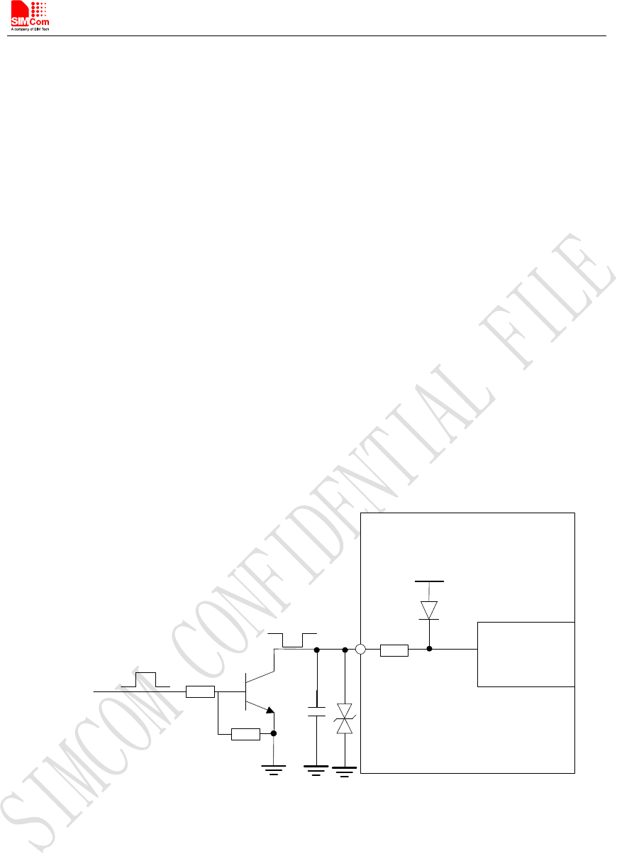
Module can be powered on by pulling the PWRKEY pin down to ground.
The PWRKEY pin has been pulled up to dVDDinternally, so you does not need to pull it up
externally. It is strongly recommended to put a100nF capacitor and an ESD protection diode close
to the PWRKEY pin. Please refer to the following figure for the recommended reference circuit.
47K
PWRKEY Power
On off logic
Diode
dVDD
MODULE
100Ω
100nF
4.7K
Turn on /off
impulse
Figure 8: ReferencePower on/offCircuit
The power-on scenarios are illustrated in the following figure.
Smart Machine Smart Decision
SIM7600A_User Manual_V1.01 2017-10-10
23
STATUS
(Output)
Ton
VBAT
PWRKEY
(Input)
Ton(status)
UART Port Undefined Active
Ton(uart)
Undefined Active
USB Port Ton(usb)
Figure 9: Power on timing sequence
Table 8: Power on timing and electronic characteristic
Symbol Parameter Min. Typ. Max. Unit
Ton The time of active low level impulse of PWRKEY
pin to power on module 100 500 - ms
Ton(status) The time from power-on issue to STATUS pin
output high level(indicating power up ready )
22 - - s
Ton(uart) The time from power-on issue to UART port ready 20 s
Ton(usb) The time from power-on issue to USB port ready 20 s
VIH Input high level voltage on PWRKEY pin 0.6 0.8 1.8 V
VIL Input low level voltage on PWRKEY pin -0.3 0 0.5 V
3.2.2 Power off
The following methods can be used to power off Module.
● Method 1: Power off Module by pulling the PWRKEY pin down to ground.
● Method 2: Power off Module by AT command“AT+ C P O F”.
● Method 3: Over-voltage or under-voltage automatic power off. The voltage range can be set by
AT command“AT + C P M V T ”.
● Method 4: Over-temperature or under-temperature automatic power off.
Note: If the temperature is outside the range of -30~+80 , some warning will be reported via
℃
AT port. If the temperature is outside the range of -40~+85 , Module will be powered off
℃
automatically.
Smart Machine Smart Decision
SIM7600A_User Manual_V1.01 2017-10-10
24
For details about “AT+CPOF” and “AT+CPMVT”, please refer to Document [1].
These procedures will make modules disconnect from the network and allow the software to enter a
safe state and save data before modules are powered off completely.
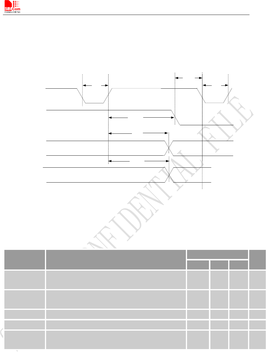
The power off scenario by pulling down the PWRKEY pin is illustrated in the following figure.
(Output)
Toff
( Input )
Toff(status)
UART Port UndefinedActive
Toff(uart)
Ton
Toff-on
USB Port Undefined
Active
Toff(usb)
PWRKEY
STATUS
Figure 10: Power off timing sequence
Table 9: Power off timing and Electronic Characteristic
Symbol Parameter Time value Unit
Min. Typ. Max.
Toff The active low level time pulse on PWRKEY pin to
power off module 2.5 -- -- s
Toff(status) The time from power-off issue to STATUS pin output
low level(indicating power off )* 22 - - s
Toff(uart) The time from power-off issue to UART port off 15 - - s
Toff(usb) The time from power-off issue to USB port off 15 - - s
Toff-on The buffer time from power-off issue to power-on
issue 0 - - s
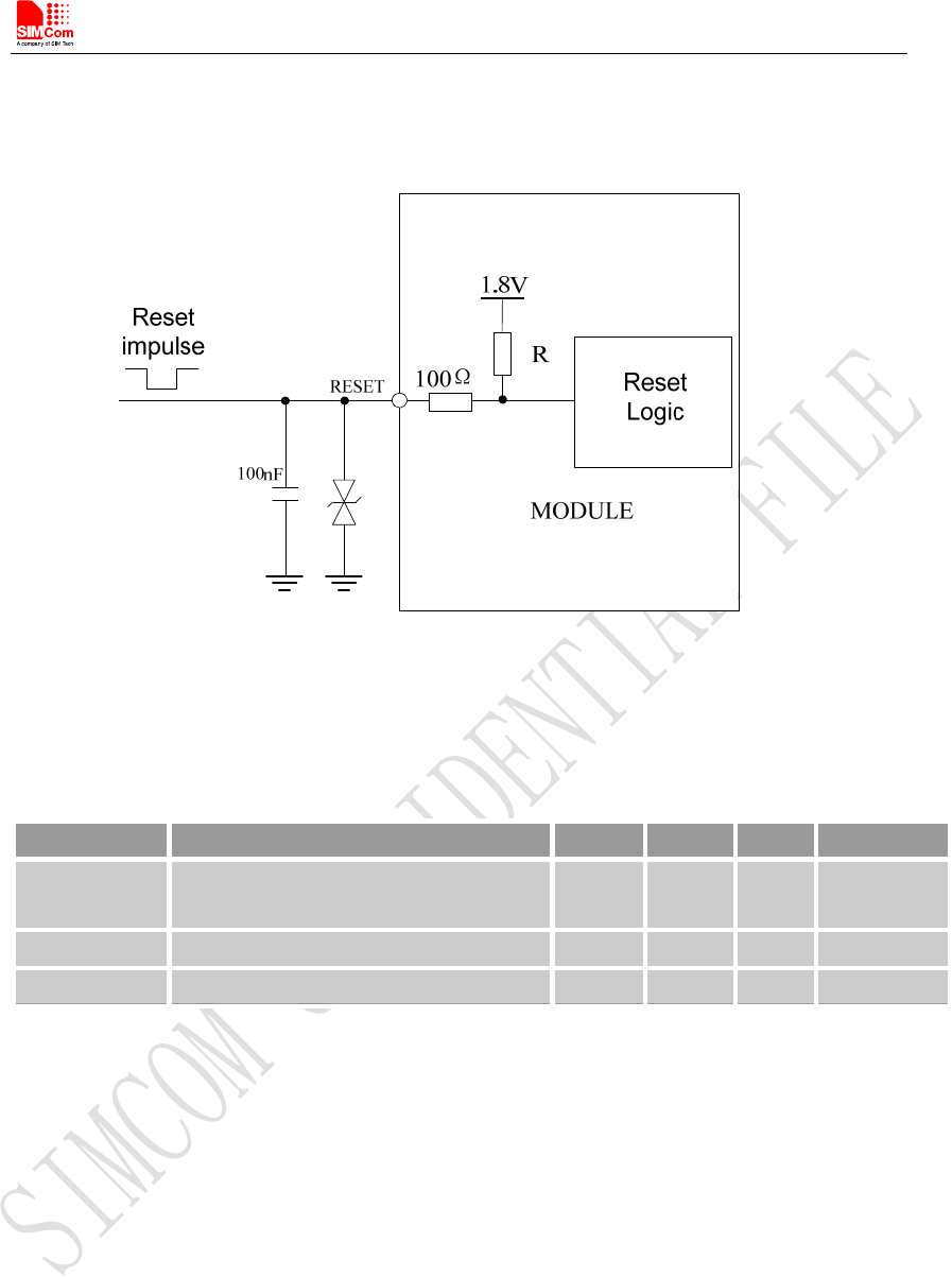
3.2.3 Reset Function
Module can be reset by pulling the RESET pin down to ground.
Note: This function is only used as an emergency reset when AT command “AT+CPOF” and the
PWRKEY pin all have lost efficacy.
Smart Machine Smart Decision
SIM7600A_User Manual_V1.01 2017-10-10
25
The RESET pin has been pulled up to 1.8V internally, so it does not need to be pulled up externally.
It is strongly recommended to put a100nF capacitor and an ESD protection diode close to the
RESET pin. Please refer to the following figure for the recommended reference circuit.
Figure 11: Reference reset circuit
Table 10: RESET pin electronic characteristic
Symbol Description Min. Typ. Max. Unit
Treset The active low level time impulse on
RESET pin to reset module 100 ms
VIH Input high level voltage 1.17 1.8 2.1 V
VIL Input low level voltage -0.3 0 0.8 V
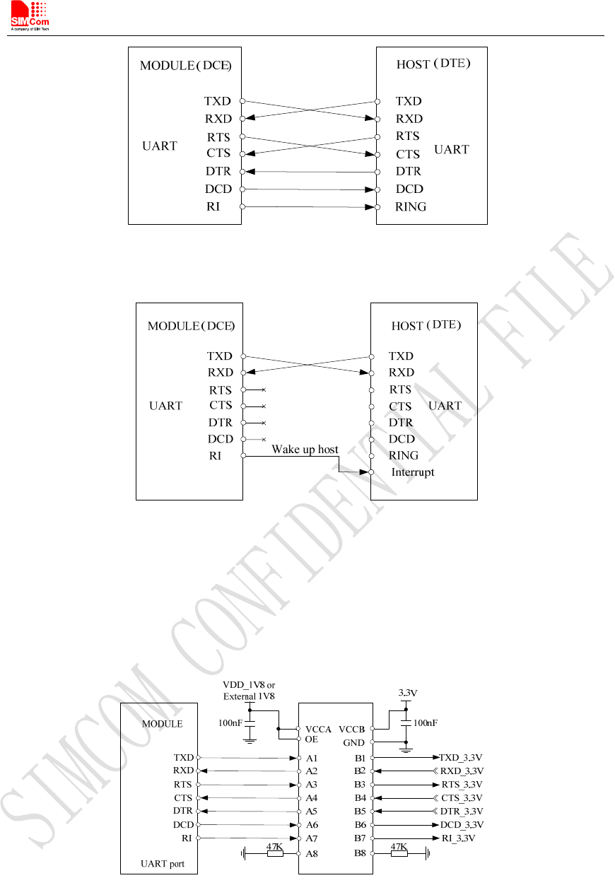
3.3 UART Interface
Module provides a 7-wire UART (universalasynchronous serial transmission) interface as DCE
(Data Communication Equipment). AT commands and data transmission can be performed through
UART interface.
3.3.1 UART Design Guide
The following figures show the reference design.
Smart Machine Smart Decision
SIM7600A_User Manual_V1.01 2017-10-10
26
Figure 12: UART full modem
Figure 13: UART null Modem
The Module UART is 1.8V voltage interface. If user’s UART application circuit is a 3.3V voltage
interface, the level shifter circuits should be used for voltage matching. The TXB0108RGYR
provided by Texas Instruments is recommended. The following figure shows the voltage matching
reference design.
Figure 14: Reference circuit of level shift
To comply with RS-232-C protocol, the RS-232-C level shifter chip should be used to connect
Module to the RS-232-C interface, for example SP3238ECA, etc.
Note: Module supports the following baud rates: 300, 600, 1200, 2400, 4800, 9600, 19200, 38400,
57600, 115200, 230400, 460800, 921600, 3200000, 3686400, 4000000bps. The default band rate
is 115200bps.
Smart Machine Smart Decision
SIM7600A_User Manual_V1.01 2017-10-10
27
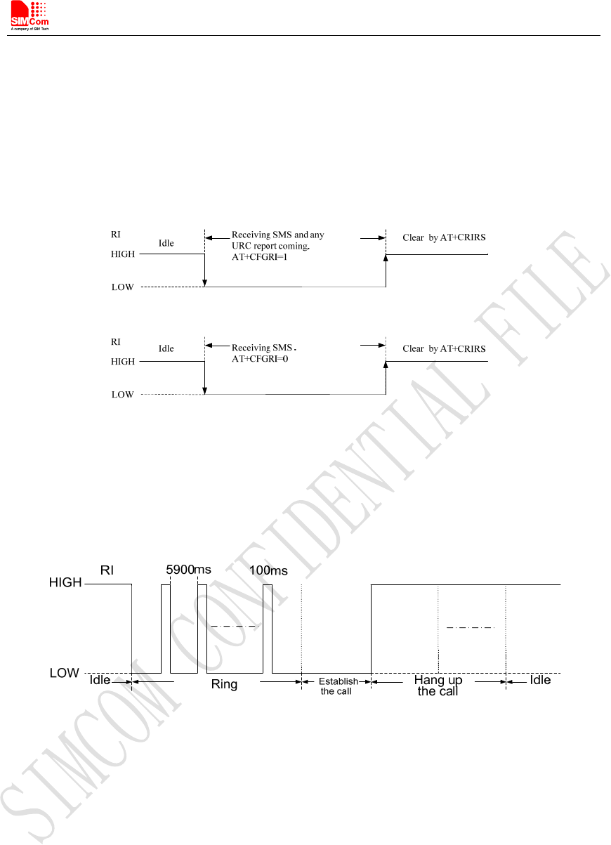
3.3.2 RI and DTR Behavior
The RI pin can be used to interrupt output signal to inform the host controller such as application
CPU.
Normally RI will stay at high level until certain conditions such as receiving SMS, or a URC report
come in. It will then change to low level. It will stay low until the host controller clears the
interrupted event with “AT+CRIRS” AT command.
Figure 15: RI behaviour(SMS and URC report)
Normally RI will be kept high until a voice call, then it will output periodic rectangular wave with
5900ms low level and 100ms high level. It will output this kind of periodic rectangular wave until
the call is answered or hung up.
Figure 16: RI behaviour(voice call)
Note: For more details of AT commands about UART, please refer to document [1] and [22].
DTR pin can be used to wake Module from sleep. When Module enters sleep mode, pulling down
DTR can wake Module.
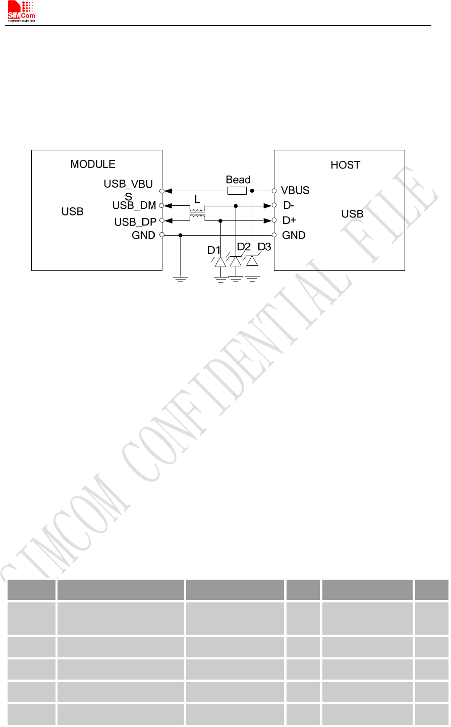
3.4 USB Interface
The Module contains a USB interface compliant with the USB2.0 specification as a peripheral, but
the USB charging function is not supported.
Smart Machine Smart Decision
SIM7600A_User Manual_V1.01 2017-10-10
28
3.4.1 USB Application Guide
Module can be used as a USB device. Module supports the USB suspend and resume mechanism
which can reduce power consumption. If there is no data transmission on the USB bus, Module will
enter suspend mode automatically and will be resumed by some events such as voice call, receiving
SMS, etc.
Figure 17: USB reference circuit
Because of the high bit rate on USB bus, more attention should be paid to the influence of the
junction capacitance of the ESD component on USB data lines. Typically, the capacitance should
be less than1pF. It is recommended to use an ESD protection component such as ESD9L5.0ST5G
provided by On Semiconductor (www.onsemi.com ).
D3 is suggested to select the diode with anti-ESD and voltage surge function, or customer could
add a ZENER diode for surge clamping. The recommend diodes list please refer to table 7.
L is recommended (MURATA) DLW21SN371SQ2L.
Note
:
The USB_DM and USB_DP nets must be traced by 90Ohm+/-10% differential
impedance.
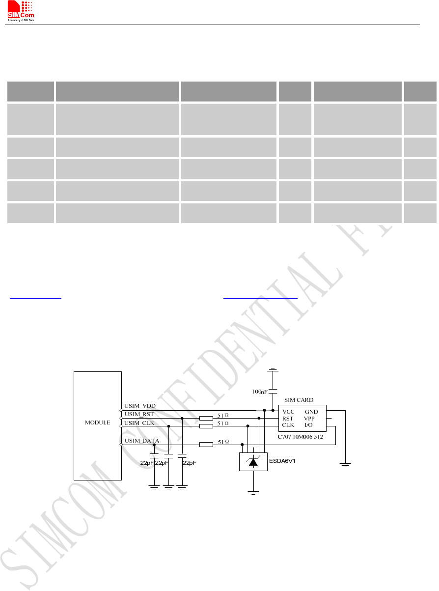
3.5 USIM Interface
Module supports both 1.8V and 3.0V USIM Cards.
Table 11: USIM Electronic characteristic in 1.8V mode (USIM_VDD=1.8V)
Symbol Parameter Min. Typ. Max. Unit
USIM_
VDD LDO power output voltage 1.75 1.8 1.95 V
VIH High-level input voltage 0.65*USIM_VDD - USIM_VDD +0.3 V
VIL Low-level input voltage -0.3 0 0.35*USIM_VDD V
VOH High-level output voltage USIM_VDD -0.45 - USIM_VDD V
VOL Low-level output voltage 0 0 0.45 V
Smart Machine Smart Decision
SIM7600A_User Manual_V1.01 2017-10-10
29
Table 12: USIM Electronic characteristic 3.0V mode (USIM_VDD=2.95V)
Symbol Parameter Min. Typ. Max. Unit
USIM_
VDD LDO power output voltage 2.75 2.95 3.05 V
VIH High-level input voltage 0.65*USIM_VDD - USIM_VDD +0.3 V
VIL Low-level input voltage -0.3 0 0.25*USIM_VDD V
VOH High-level output voltage USIM_VDD -0.45 - USIM_VDD V
VOL Low-level output voltage 0 0 0.45 V
3.5.1 USIM Application Guide
It is recommended to use an ESD protection component such as ESDA6V1W5 produced by ST
(www.st.com ) or SMF15C produced by ON SEMI (www.onsemi.com ). Note that the USIM
peripheral circuit should be close to the USIM card socket.The following figure shows the 6-pin
SIM card holder reference circuit.
Figure 18: USIM interface reference circuit
Note: USIM_DATA has been pulled up with a100KΩ resistor to USIM_VDD in module. A 100nF
capacitor on USIM_VDD is used to reduceinterference. For more details of AT commands about
USIM, please refer to document [1].
3.5.2 SIM Card Design Guide
SIM card signal could be interferenced by some high frequency signal, it is strongly recommended
to follow these guidelines while designing:
SIM card holder should be far away from antenna
SIM traces should keep away from RF lines, VBAT and high-speed signal lines
Smart Machine Smart Decision
SIM7600A_User Manual_V1.01 2017-10-10
30
The traces should be as short as possible
Keep SIM card holder’s GND connect to main ground directly
Shielding the SIM card signal by ground well
Recommended to place a 100nF capacitor on SIM_VDD line and keep close to the SIM
card holder
Add some TVS which parasitic capacitance should not exceed 50pF
Add 51Ω resistor to (SIM_RST/SIM_CLK/SIM_DATA) signal could enhance ESD
protection
Add 22pF capacitor to (SIM_RST/SIM_CLK/SIM_DATA) signal to induce RF signal
interference
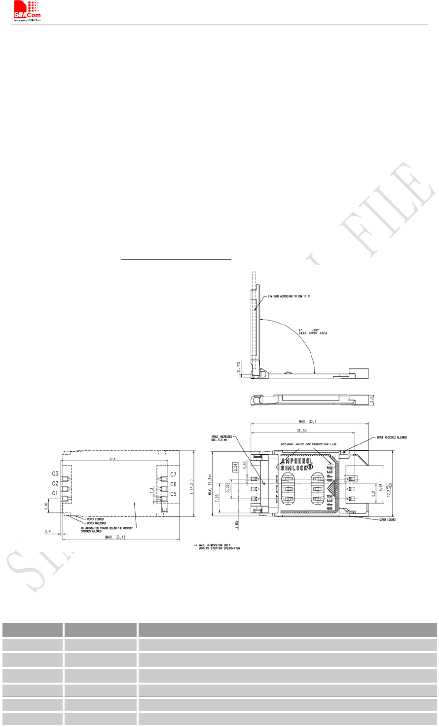
3.5.3 Recommended USIM Card Holder
It is recommended to use the 6-pin USIM socket such as C707 10M006 512 produced by
Amphenol. User can visit http://www.amphenol.com for more information about the holder.
Figure 19: Amphenol SIM card socket
Table 13: Amphenol USIM Socket Pin Description
Pin Signal Description
C1 USIM_VDD USIM Card Power supply.
C2 USIM_RST USIM Card Reset.
C3 USIM_CLK USIM Card Clock.
C5 GND Connect to GND.
C6 VPP
C7 USIM_DATA USIM Card data I/O.
Smart Machine Smart Decision
SIM7600A_User Manual_V1.01 2017-10-10
31
3.6 PCM Interface
Module provides a PCM interface for external codec, which can be used inmaster mode with short
sync and 16 bits linear format.
Table 14: PCM Format
Note: For more details about PCM AT commands, please refer to document [1].
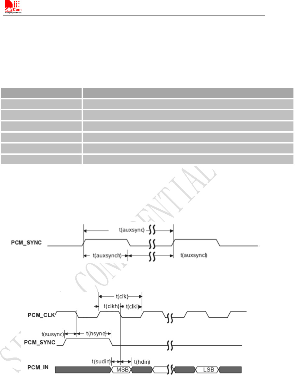
3.6.1 PCM Timing
Module supports 2.048 MHz PCM data and sync timing for 16 bits linear format codec.
Figure 20: PCM_SYNC timing
Figure 21: EXT codec to module timing
Characteristics Specification
LineInterfaceFormat Linear(Fixed)
Datalength 16bits(Fixed)
PCM Clock/Sync Source Master Mode(Fixed)
PCMClockRate 2048 KHz (Fixed)
PCMSyncFormat Shortsync(Fixed)
Data Ordering MSB
Smart Machine Smart Decision
SIM7600A_User Manual_V1.01 2017-10-10
32
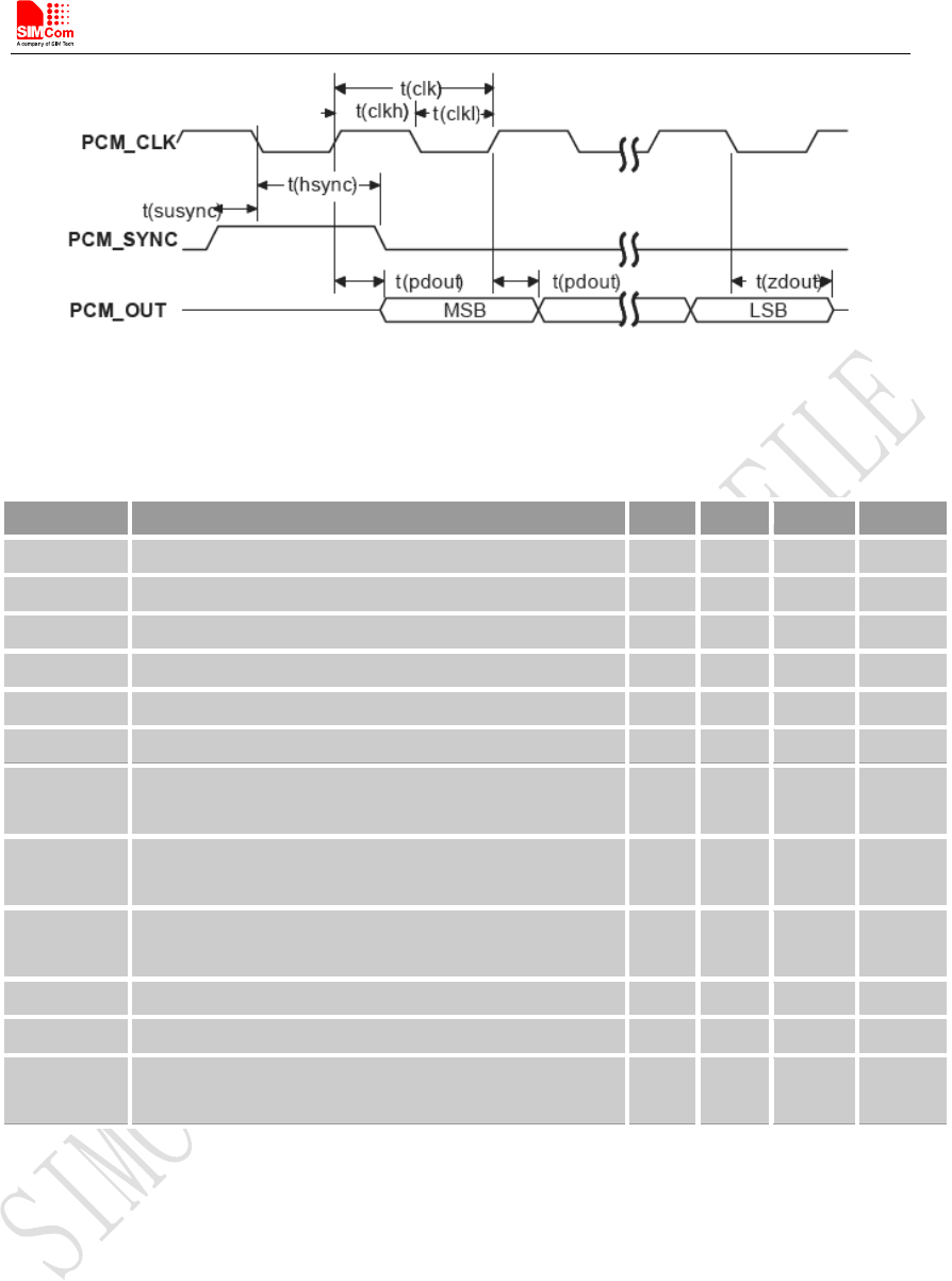
Figure 22: Module to EXT codec timing
Table 15: PCM Timing Parameters
Parameter Description Min. Typ. Max. Unit
T(sync) PCM_SYNC cycle time – 125 – μs
T(synch) PCM_SYNC high level time – 488 – ns
T(syncl) PCM_SYNC low level time – 124.5 – μs
T(clk) PCM_CLK cycle time – 488 – ns
T(clkh) PCM_CLK high level time – 244 – ns
T(clkl) PCM_CLK low level time – 244 – ns
T(susync) PCM_SYNC setup time high before falling edge of
PCM_CLK – 122 – ns
T(hsync) PCM_SYNC hold time after falling edge of
PCM_CLK – 366 – ns
T(sudin) PCM_IN setup time before falling edge of
PCM_CLK 60 – – ns
T(hdin) PCM_IN hold time after falling edge of PCM_CLK 60 – – ns
T(pdout) Delay from PCM_CLK rising to PCM_OUT valid – – 60 ns
T(zdout) Delay from PCM_CLK falling to PCM_OUT
HIGH-Z – – 60 ns
3.6.2 PCM Application Guide
The following figure shows the external codec reference design.
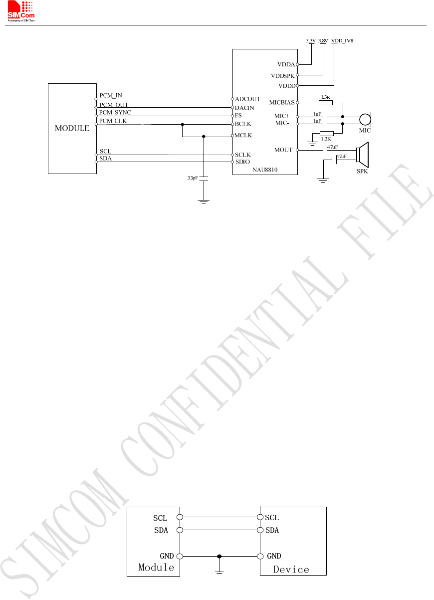
Smart Machine Smart Decision
SIM7600A_User Manual_V1.01 2017-10-10
33
Figure 23: Audio codec reference circuit
Note: Module can transmit PCM data by theUSB portbesidesthe PCM interface. For more
details please refer to documents [1] and [23].
3.7 I2C Interface
Module provides a I2C interface compatible with I2C specification, version 2.1, with clock rate up
to 400 kbps. Its operation voltage is 1.8V.
3.7.1 I2C Design Guide
The following figure shows the I2C bus reference design.
Figure 24: I2C reference circuit
Note
:
SDA and SCLhave pull-up resistors in module. So, 2 external pull up resistors are not needed in
application circuit.
“AT+CRIIC and AT+CWIIC” AT commands could be used to read/write register values of the
I2C peripheral devices.For more details about AT commands please refer to document [1].
Smart Machine Smart Decision
SIM7600A_User Manual_V1.01 2017-10-10
34
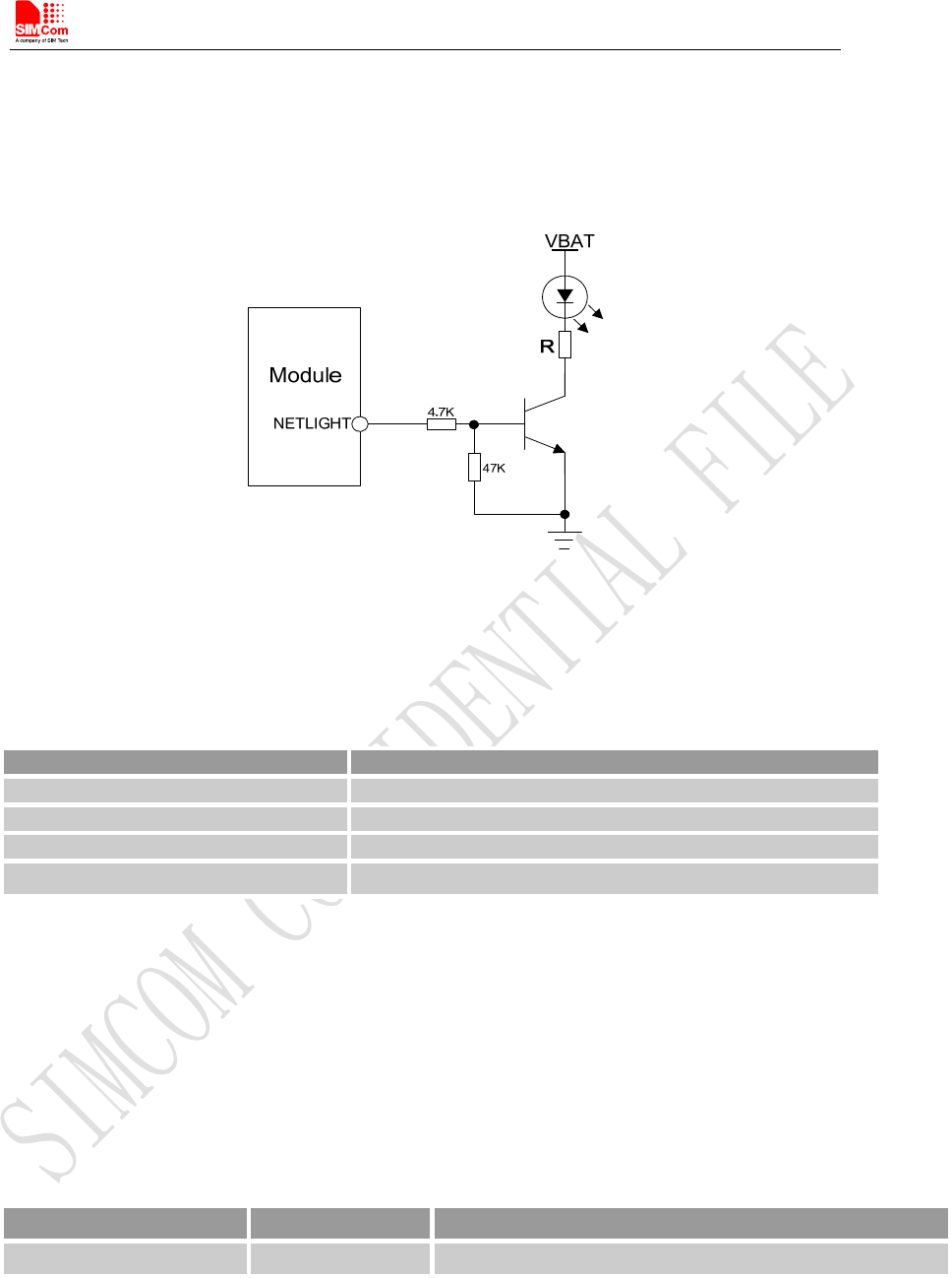
3.8 Network Status
The NETLIGHT pin is used to control Network Status LED, its reference circuit is shown in the
following figure.
Figure 25: NETLIGHT reference circuit
Note: The value of the resistor named “R” depends on the LED characteristic.
Table 16: NETLIGHT pin status
NETLIGHT pin status Module status
Always On Searching Network/Call Connect
200ms ON, 200ms OFF Data Transmit
800ms ON, 800ms OFF Registered network
OFF Power off / Sleep
Note: NETLIGHT output low level as “OFF”, and high level as “ON”.
3.9 Operating Status Indication
The pin50 is for operating status indication of the module. The pin output is high when module is
powered on, and output is low when module is powered off.
Table 17: Pin definition of the STATUS
Pin name Pin number Description
STATUS 50 Operating status indication
Note: For timing about STATUS, please reference to the chapter “3.2 power on/down scenarios”
3.10 Pin Multiplex Function
Some pins of Module could be used for alternate function besides default function.
Smart Machine Smart Decision
SIM7600A_User Manual_V1.01 2017-10-10
35
Table 18: Pin multiplex function list
Note
:
For more details of AT commands about GPIO multiplex function,please refer to
document [1].
3.11 Other interface
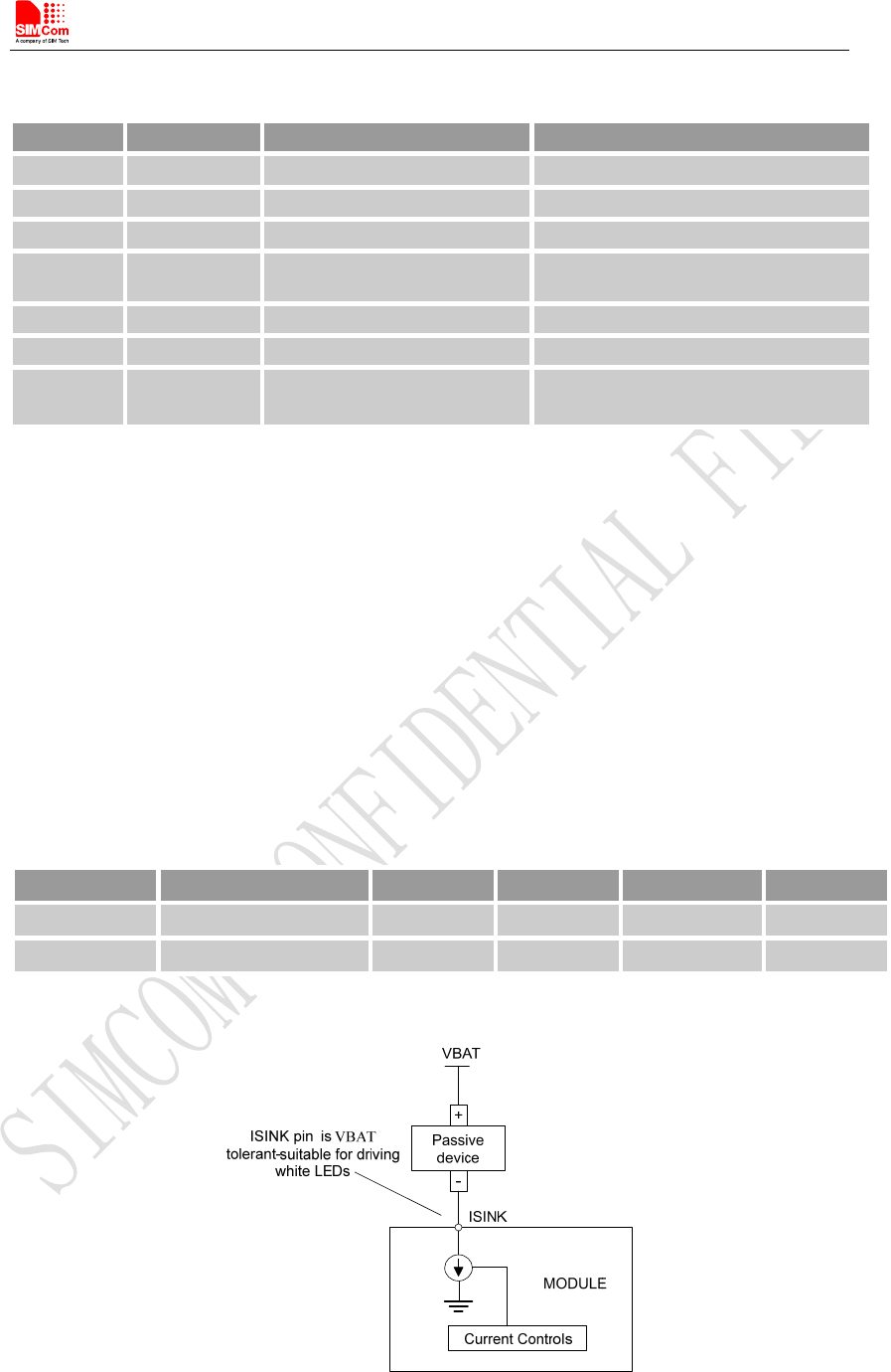
3.11.1 Sink Current Source
The ISINK pin is VBATtolerant and intended to drive some passive devices such as LCD backlight,
white LED, etc. Its output current can be up to 40 mA and be set by the AT command “AT+
CLEDITST”.
Table 19: Sink current electronic characteristic
Symbol Description Min. Typ. Max. Unit
VISINK Voltage tolerant 0.5 - VBAT V
IISINK Current tolerant 0 - 40 mA
ISINK is a ground-referenced current sink. The following figure shows its reference circuit.
Figure 26: ISINK reference circuit
Pin Number Pin Name Default Function Alternate Function
4 SCL SCL GPIO11
5 SDA SDA GPIO10
12 USIM_DET GPIO34 USIM_DET
18 PCM_CLK PCM_CLK GPIO23,SPI_CLK
I2C_SCL
19 PCM_SYNC PCM_SYNC GPIO20,SPI_MOSI
20 PCM_IN PCM_IN, GPIO21,SPI_MISO
21 PCM_OUT PCM_OUT GPIO22,SPI_CS_N
I2C_SDA
Smart Machine Smart Decision
SIM7600A_User Manual_V1.01 2017-10-10
36
Note: The sinking current can be adjusted to meet the design requirement through the AT
command “AT+ CLEDITST =<0>, <value>”.The “value” ranges from 0 to 8, on behalf of the
current from 0mA to 40mA by 5mA step.
3.11.2 ADC
Module has 1 dedicated ADC pins named ADC. They are available fordigitizing analog signals
such as battery voltage and so on. These electronic specifications are shown in the following table.
Table 20: ADC Electronic Characteristics
Characteristics Min. Typ. Max. Unit
Resolution –15 – Bits
Input Range 0.1 1.7 V
Input serial resistance 1 – – MΩ
Note: “AT+CADC” can be used to read the voltage of the ADC pins, for more details, please
refer to document [1].
Smart Machine Smart Decision
SIM7600A_User Manual_V1.01 2017-10-10
37
4 RF Specifications
4.1 WCDMA/LTE RF Specifications
Table 21: Conducted transmission power
Frequency Power Min.
WCDMA B2 24dBm +1/-3dB <-50dBm
WCDMA B5 24dBm +1/-3dB <-50dBm
LTE-FDD B2 23dBm +/-2.7dB <-40dBm
LTE-FDD B4 23dBm +/-2.7dB <-40dBm
LTE-FDD B12 23dBm +/-2.7dB <-40dBm
Table 22: Operating frequencies
Frequency Receiving Transmission
WCDMA B2 1930~1990 MHz 1850~1910 MHz
WCDMA B5 869~894 MHz 824~849 MHz
LTE-FDD B2 1930 ~1990 MHz 1850 ~1910 MHz
LTE-FDD B4 2110~2155 MHz 1710 ~1755 MHz
LTE-FDD B12 729~746 MHz 699 ~716 MHz
Table 23: Conducted receive sensitivity
Frequency Receive sensitivity(Typical) Receive sensitivity(MAX)
WCDMA B2 < -110dBm 3GPP
WCDMA B5 < -110dBm 3GPP
LTE See table 24 3GPP
Table 24: Reference sensitivity (QPSK)
E-UTRA
band
3GPP standard Test value 3GPP standard Duplex
1.4 MHz 3MHz 5MHz 10MHz 10 MHz 15 MHz 20 MHz
2 -102.7 -99.7 -98 -95 -101 -93.2 -92 FDD
4 -104.7 -101.7 -100 -97 -102 -95.2 -94 FDD
12 -101.7 -98.7 -97 -94 -101.5 FDD
Smart Machine Smart Decision
SIM7600A_User Manual_V1.01 2017-10-10
38
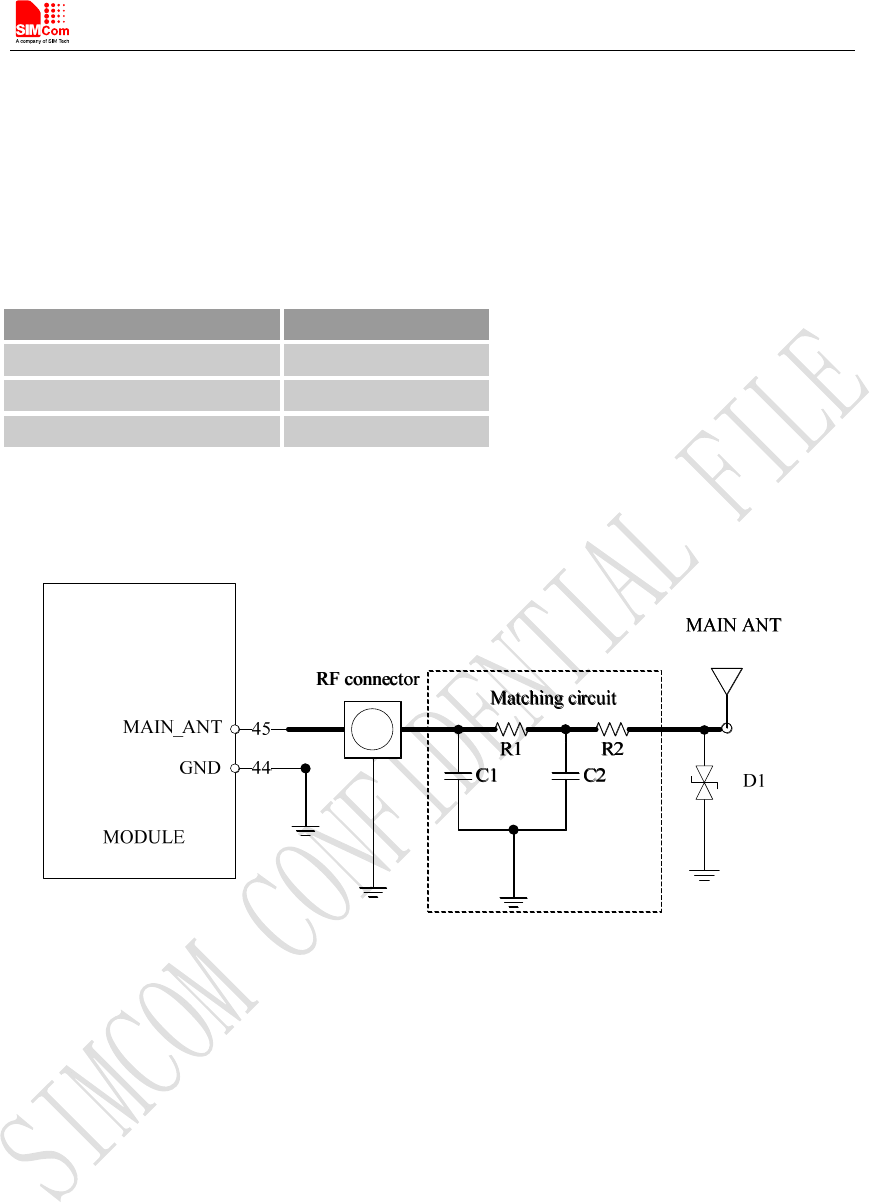
4.2 WCDMA/LTE Antenna Design Guide
Users should connect antennas to Module’s antenna pads through the micro-strip line or other types
of RF trace. The trace impedance must be controlled in 50Ω. SIMCom recommends that the total
insertion loss between Module and antenna should meet the following requirements:
Table 25: Trace Loss
Frequency Loss
700MHz-960MHz <0.5dB
1710MHz-2170MHz <0.9dB
2300MHz-2650MHz <1.2dB
To facilitate the antenna tuning and certification test, a RF connector and an antenna matching
circuit should be added. The following figure is the recommended circuit.
Figure 27: Antenna matching circuit (MAIN_ANT)
In above figure, the components R1,C1,C2 and R2 are used for antenna matching, the value of
components can only be achieved after the antenna tuning and usually provided by antenna vendor.
By default, the R1, R2 are 0Ω resistors, and the C1, C2 are reserved for tuning. The component D1
is a TVS for ESD protection, and it is optional for users according to application environment.
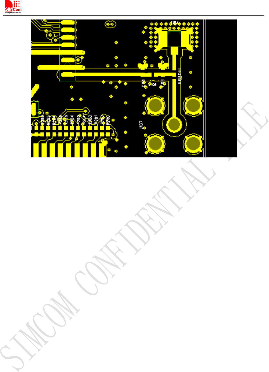
The RF test connector is used for the conducted RF performance test, and should be placed as close
as to the module’s MAIN_ANT pin. The traces impedance between Module and antenna must be
controlled in 50Ω.
Smart Machine Smart Decision
SIM7600A_User Manual_V1.01 2017-10-10
39
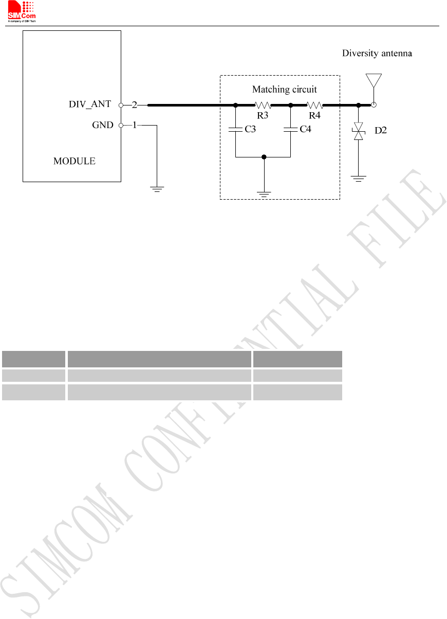
Figure 28: Antenna matching circuit (DIV_ANT)
In above figure, R3, C3, C4 and R4 are used for auxiliary antenna matching. By default, the R3, R4
are 0Ωresistors, and the C3, C4 are reserved for tuning. D2 is a TVS for ESD protection, and it is
optional for users according to application environment.
Two TVS are recommended in the table below.
Table 26: Recommended TVS
Package Part Number Vender
0201 LXES03AAA1-154 Murata
0402 LXES15AAA1-153 Murata
Note
:
SIMCom suggests the LTE auxiliary antenna to be kept on, since there are many high
bands in the designing of FDD-LTE. Because of the high insert loss of the RF cable and layout
lines, the receiver sensitivity of these bands above will have risk to meet the authentication
without the diversity antenna.For more details about auxiliary antenna design notice,please
refer to document [25]
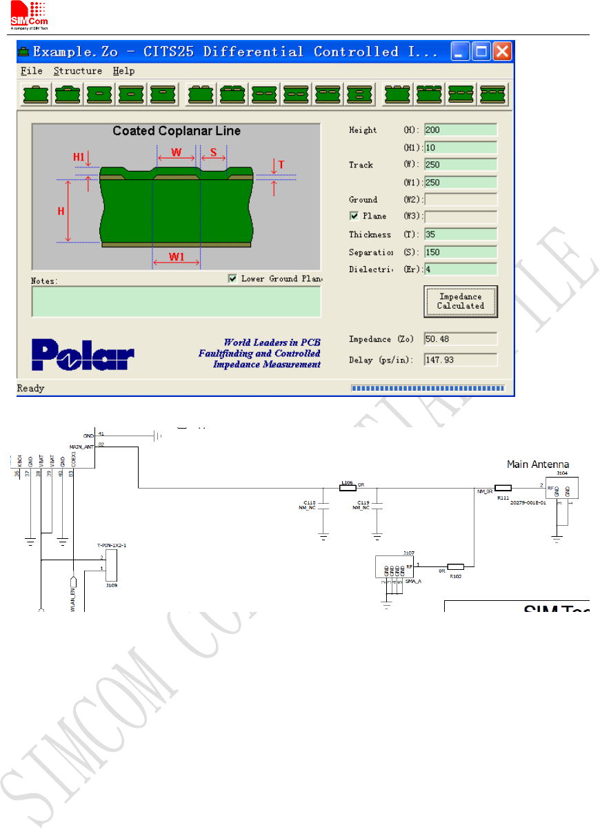
To facilitate the antenna tuning and certification test, a RF connector and an antenna matching
circuit should be added. The following figure is the recommended circuit.
circuit should be added. The following figure is the recommended circuit.
Smart Machine Smart Decision
SIM7600A_User Manual_V1.01 2017-10-10
40
Smart Machine Smart Decision
SIM7600A_User Manual_V1.01 2017-10-10
41
Figure 29: Antenna matching circuit (MAIN_ANT)
In figure 29, the components L106, C118, C119 and R111 or R102 are used for antenna matching,
the values of components can only be achieved after the antenna tuning and usually provided by
antenna vendor. By default, the L106,R111or R102 are 0Ω resistors, and the C118, C119 are
reserved for tuning are reserved for tuning. The RF test connector is used for the conducted RF
performance test, and should be placed as close as to the module’s MAIN_ANT pin. The traces
impedance between module and antenna must be controlled in 50Ω.
4.3 GNSS
SIM7600A merges GNSS satellite and network information to provide a high-availability solution
that offers industry-leading accuracy and performance. This solution performs well, even in very
challenging environmental conditions where conventional GNSS receivers fail, and provides a
platform to enable wireless operators to address both location-based services and emergency
mandates.
4.3.1 GNSS Technical specification
Tracking sensitivity: -159 dBm(GPS)/-158 dBm(GLONASS)
Cold-start sensitivity: -148 dBm
Accuracy (Open Sky): 2.5m (CEP50)
TTFF (Open Sky) : Hot start <1s, Cold start<35s
Receiver Type: 16-channel, C/A Code
GPS L1 Frequency: 1575.42±1.023MHz
GLONASS: 1597.5~1605.8 MHz
Update rate: Default 1 Hz
Smart Machine Smart Decision
SIM7600A_User Manual_V1.01 2017-10-10
42
GNSS data format: NMEA-0183
GNSS Current consumption : 100mA ((WCDMA/LTE Sleep ,in total on VBAT pins)
GNSS antenna: Passive/Active antenna
Note: If the antenna is active type, the power should be given by main board, because there is no
power supply on GPS antenna pad. If the antenna is passive, it is suggested that the external
LNA should be used.
4.3.2 GNSS Application Guide
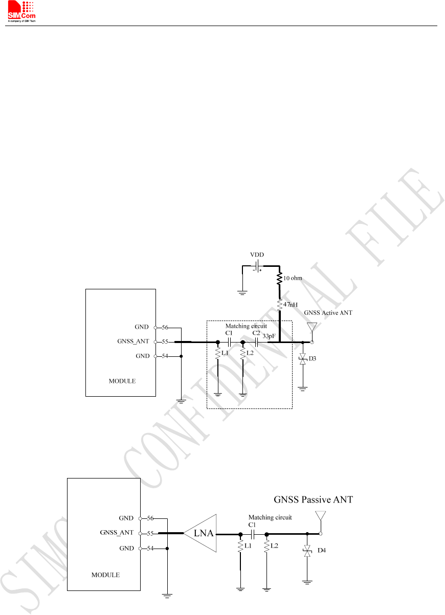
Users can adopt an active antenna or a passive antenna as GNSS signal transceiver. In this
document, all GNSS specification mentioned is from passive antenna. The following is the
reference circuit.
Figure 30: Active antenna circuit
Figure 31: Passive antenna circuit (Default)
In above figures, the components C1 and L1, L2 are used for antenna matching, the values of the
components can only be obtained after the antenna tuning and usually provided by antenna vendor.
C2 in Figure 29 is used for DC blocking. L3 is the matching component of the external LNA, and
the value of L3 is determined by the LNA characteristic and PCB layout. Both VDD of active
antenna and V_LNA need external power supplies which should be considered according to active
antenna and LNA characteristic. LDO/DCDC is recommended to get lower current consuming by
shutting down active antennas and LNA when GNSS is not working.
Smart Machine Smart Decision
SIM7600A_User Manual_V1.01 2017-10-10
43
LNA should apply the following requirements as table 28. LNA is also suggested to put near the
passive antenna.
Table 27: LNA requirements
Parameter Min Max Unit
Vdd 1.5 3.3 V
Idd 3 mA
LNA_EN 1.3 V
Gain 14 17 dB
VSWR 2
GNSS can be used by NMEA port. User can select NMEA as output through UART or USB.
NMEA sentences are automatic and no command is provided. NMEA sentences include GSV, GGA,
RMC, GSA, and VTG. Before using GNSS, user should configure SIM7600A in proper operating
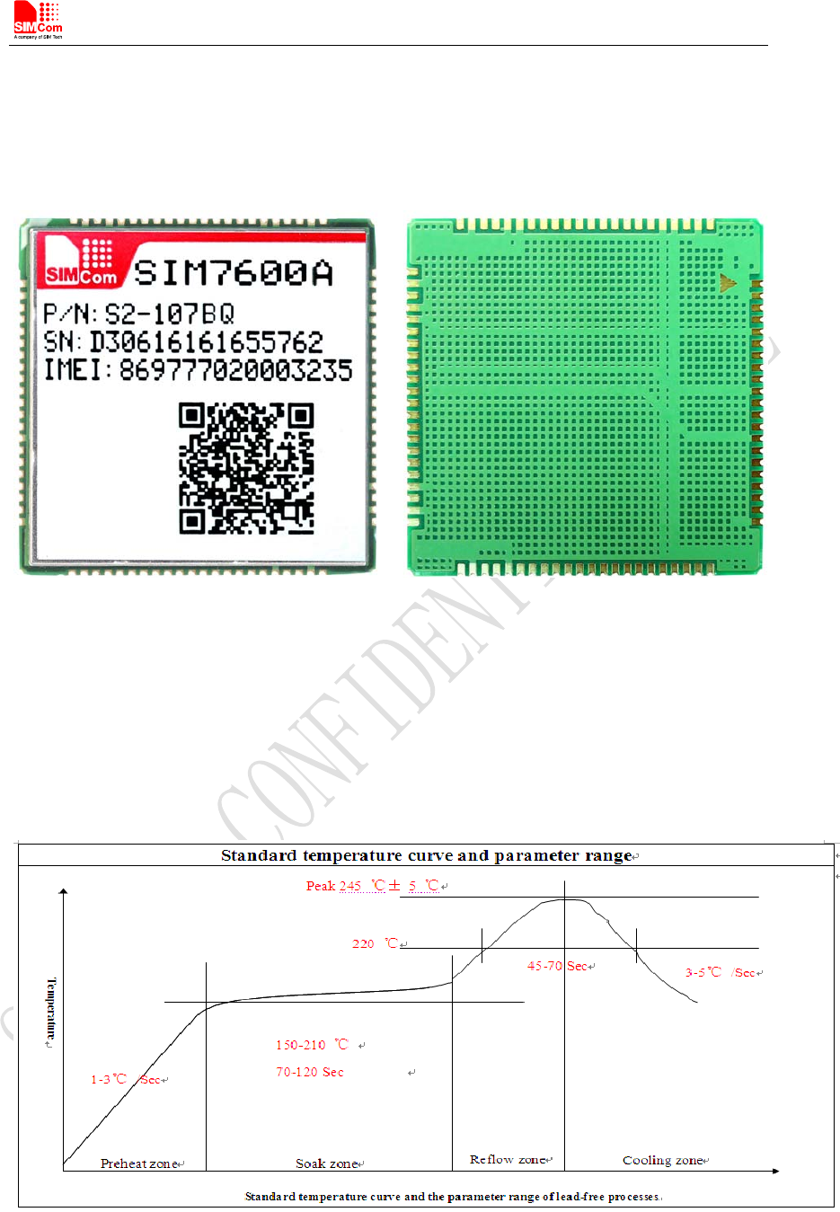
mode by AT command. Please refer to related document for details. SIM7600A can also get
position location information through AT directly.
Note: GNSS is closed by default, it could be started by AT+CGPS. The AT command has two
parameters, the first is on/off, and the second is GNSS mode. Default mode is standalone mode.
AGPS mode needs more support from the mobile telecommunication network. Please refer to
document [24] for more details.
Smart Machine Smart Decision
SIM7600A_User Manual_V1.01 2017-10-10
44
5 Electrical Specifications
5.1 Absolute Maximum Ratings
Absolute maximumrating for digital and analog pins of Module are listed in the following table:
Table 28: Absolute maximum ratings
Parameter Min. Max. Unit
Voltage at VBAT -0.5 6.0 V
Voltage at VBUS -0.5 6.3 V
Voltage at digital pins (RESET,SPI,GPIO,I2C,UART,PCM) -0.3 2.1 V
Voltage at digital pins :USIM -0.3 3.05 V
Voltage at PWRKEY -0.3 1.8
5.2 Operating Conditions
Table 29: Recommended operating ratings
Parameter Min. Typ. Max. Unit
Voltage at VBAT 3.4 3.8 4.2 V
Voltage at VBUS 3.6 5 5.25 V
Table 30: 1.8V Digital I/O characteristics*
Parameter Description Min. Typ. Max. Unit
VIH High-level input voltage 1.17 1.8 2.1 V
VIL Low-level input voltage -0.3 0 0.63 V
VOH High-level output voltage 1.35 - 1.8 V
VOL Low-level output voltage 0 - 0.45 V
IOH High-level output current(no
pull down resistor) - 2 mA
IOL Low-level output current(no pull
up resistor) - -2 - mA
IIH Input high leakage current (no
pull down resistor) - - 1 uA
IIL Input low leakage current(no
pull up resistor) -1 - - uA
*Note: These parameters are for digital interface pins, such as SPI, GPIOs (NETLIGHT), I2C,
UART, PCM.
Smart Machine Smart Decision
SIM7600A_User Manual_V1.01 2017-10-10
45
The operating temperature of Module is listed in the following table.
Table 31: Operating temperature
Parameter Min. Typ. Max. Unit
Normal operation temperature -30 25 80 ℃
Extended operation temperature* -40 25 85 ℃
Storage temperature -45 25 +90 ℃
*Note: Module is able to make and receive voice calls, data calls, SMS and make
WCDMA/HSPA+/LTE traffic in -40℃ ~ +85℃. The performance will be reduced slightly from
the 3GPP specifications if the temperature is outside the normal operating temperature range
and still within the extreme operating temperature range.
5.3 Operating Mode
5.3.1 Operating Mode Definition
The table belowsummarizes the various operating modes of Module series products.
Table 32: Operating mode Definitions
Mode Function
Normal operation
GSM/WCDMA / LTE
Sleep
In this case, the current consumption of module will be reduced to the
minimal level and the module can still receive paging message and
SMS.
GSM/WCDMA / LTE
Idle
Software is active. Module is registered to the network, and the
module is ready to communicate.
GSM/WCDMA / LTE
Talk
Connection between two subscribers is in progress. In this case, the
power consumption depends on network settings such as DTX off/on,
FR/EFR/HR, hopping sequences, antenna.
GSM/WCDMA/LTE
Standby
Module is ready for data transmission, but no data is currently sent or
received. In this case, power consumption depends on network
settings.
GPRS/EDGE/WCDM
A / LTE transmission
There is data transmission in progress. In this case, power
consumption is related to network settings (e.g. power control level);
uplink/downlink data rates, etc.
Minimum functionality
mode
AT command “AT+CFUN=0” can be used to set the module to a
minimum functionality mode without removing the power supply. In
this mode, the RF part of the module will not work and the USIM
card will not be accessible, but the serial port and USB port are still
accessible. The power consumption in this mode is lower than normal
mode.
Flight mode AT command “AT+CFUN=4” or pulling down the FLIGHTMODE
pin can be used to set the module to flight mode without removing the

Smart Machine Smart Decision
SIM7600A_User Manual_V1.01 2017-10-10
46
power supply. In this mode, the RF part of the module will not work
but the serial port and USB port are still accessible. The power
consumption in this mode is lower than normal mode.
Power off
Module will go into power off mode by sending the AT command
“AT+CPOF” or by pulling down the PWRKEY pin normally. In this
mode the power management unit shuts down the power supply and
software is not active. The serial port and USB are is not accessible.
5.3.2 Sleep Mode
In sleep mode, the current consumption of module will be reduced to the minimal level, and
module can still receive paging message and SMS.
Several hardware and software conditions must be satisfied together in order to let Module enter
into sleep mode:
1. UART condition
2. USB condition
3. Software condition
Note: Before designing, pay attention to how to realize sleeping/waking function and refer to
Document [26] for more details.
5.3.3 Minimum Functionality Mode and Flight Mode
Minimum functionality mode ceasesa majority functionof module, thus minimizing the power
consumption. This mode is set by the AT command which provides a choice of the functionality
levels.
● AT+CFUN=0: Minimum functionality
● AT+CFUN=1: Full functionality (Default)
● AT+CFUN=4: Flight mode
If Module has been set to minimum functionality mode, the RF function and USIM card function
will be closed. In this case, the serial port and USB are still accessible, but RF function and USIM
card will be unavailable.
If Module has been set to flight mode, the RF function will be closed. In this case, the serial port
and USB are still accessible, but RF function will be unavailable.
When Module is in minimum functionality or flight mode, it can return to full functionality by the
AT command “AT+CFUN=1”.
5.4 Current Consumption
The current consumption is listed in the table below.
Smart Machine Smart Decision
SIM7600A_User Manual_V1.01 2017-10-10
47
Table 33: Current consumption on VBAT Pins (VBAT=3.8V)
UMTS Sleep/Idle Mode
WCDMA supply current
(without USB connection)
Sleep mode @DRX=9Typical: 1.11
Idle mode @DRX=9Typical: 17.5
LTE Sleep/Idle mode
LTE supply current
(without USB connection)
Sleep mode Typical: 1.56
Idle mode Typical: 22
UMTS Talk
WCDMA B2 @Power 22dBm Typical: 524mA
WCDMA B5 @Power 23.48dBm Typical: 480mA
HSDPA Data
WCDMA B2 @Power 24dBm Typical: TBD
WCDMA B5 @Power 24dBm Typical: TBD
LTE Data
LTE-FDD B2
@5 MHz 22.2dBm Typical: 589mA
@10 MHz 22.7dBm Typical: 577mA
@20 MHz 22.38dBm Typical: 626mA
LTE-FDD B4
@5 MHz 23.05dBm Typical: 519mA
@10 MHz 23.04dBm Typical: 556mA
@20 MHz 22.83dBm Typical: 600mA
LTE-FDD B12 @5 MHz 22.69dBm Typical: 516mA
@10 MHz 22.9dBm Typical: 512mA
5.5 ESD Notes
Module is sensitive to ESD in the process of storage, transporting and assembling. Especially,
Module is mounted on the users’ mother board, The ESD components should be placed beside the
connectors which human body might touch, such as USIM card holder, audio jacks, switches and
keys, etc. The following table shows the Module ESD measurement performance without any
external ESD component.
Table 34: The ESD performance measurement table (Temperature: 25℃, Humidity: 45%)
Part Contact discharge Air discharge
GND +/-6K +/-12K
VBAT +/-5K +/-10K
Antenna port +/-5K +/-10K
USB +/-4K +/-8K
UART +/-4K +/-8K
PCM +/-4K +/-8K
Other PADs +/-3K +/-6K
Smart Machine Smart Decision
SIM7600A_User Manual_V1.01 2017-10-10
48
6 SMT Production Guide
6.1 Top and Bottom View of Module
Figure 32: Top and bottom view of Module
6.2 Typical SMT Reflow Profile
SIMCom provides a typical soldering profile. Therefore the soldering profile shown below is only
a generic recommendation and should be adjusted to the specific application and manufacturing
constraints.
Figure 33: The ramp-soak-spike Reflow Profile of Module
Note: For more details about secondary SMT, please refer to the document [21].
Smart Machine Smart Decision
SIM7600A_User Manual_V1.01 2017-10-10
49
6.3 Moisture Sensitivity Level (MSL)
Module is qualified to Moisture Sensitivity Level (MSL) 3 in accordance with JEDEC J-STD-033.
If the prescribed time limit is exceeded, users should bake modules for 192 hours in drying
equipment (<5% RH) at 40+5/-0°C, or 72 hours at 85+5/-5°C. Note that plastic tray is not
heat-resistant, and only can be baked at 45° C.
Table 35: Moisture Sensitivity Level and Floor Life
Moisture Sensitivity Level
(MSL)
Floor Life (out of bag) at factory ambient≤30°C/60% RH or as
stated
1 ≦℃
Unlimited at 30 /85% RH
2 1 year
2a 4 weeks
3 168 hours
4 72 hours
5 48 hours
5a 24 hours
6 Mandatory bake before use. After bake, it must be reflowed within the
time limit specified on the label.
NOTE: IPC / JEDEC J-STD-033 standard must be followed for production and storage.
6.4 Stencil Foil Design Recommendation
The recommended thickness of stencil foil is more than 0.1mm.
Smart Machine Smart Decision
SIM7600A_User Manual_V1.01 2017-10-10
50
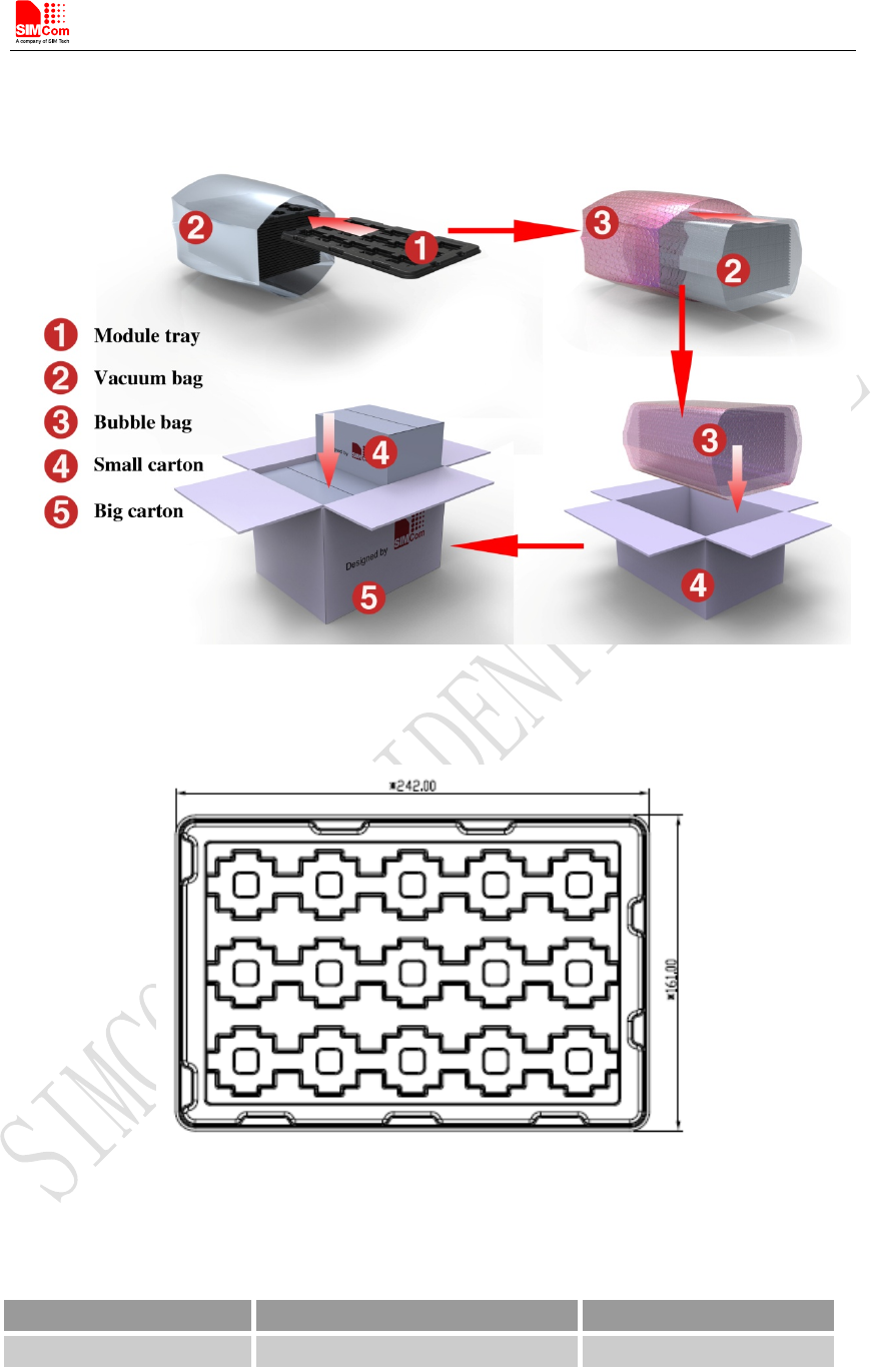
7 Packaging
Module module support tray packaging.
Figure 34: Packaging introduce
Module tray drawing:
Figure 35: Module tray drawing introduce
Table 36: Tray size
Length(±3mm) Width(±3mm) Module number
242.0 161.0 15
Small carton drawing:
Smart Machine Smart Decision
SIM7600A_User Manual_V1.01 2017-10-10
51
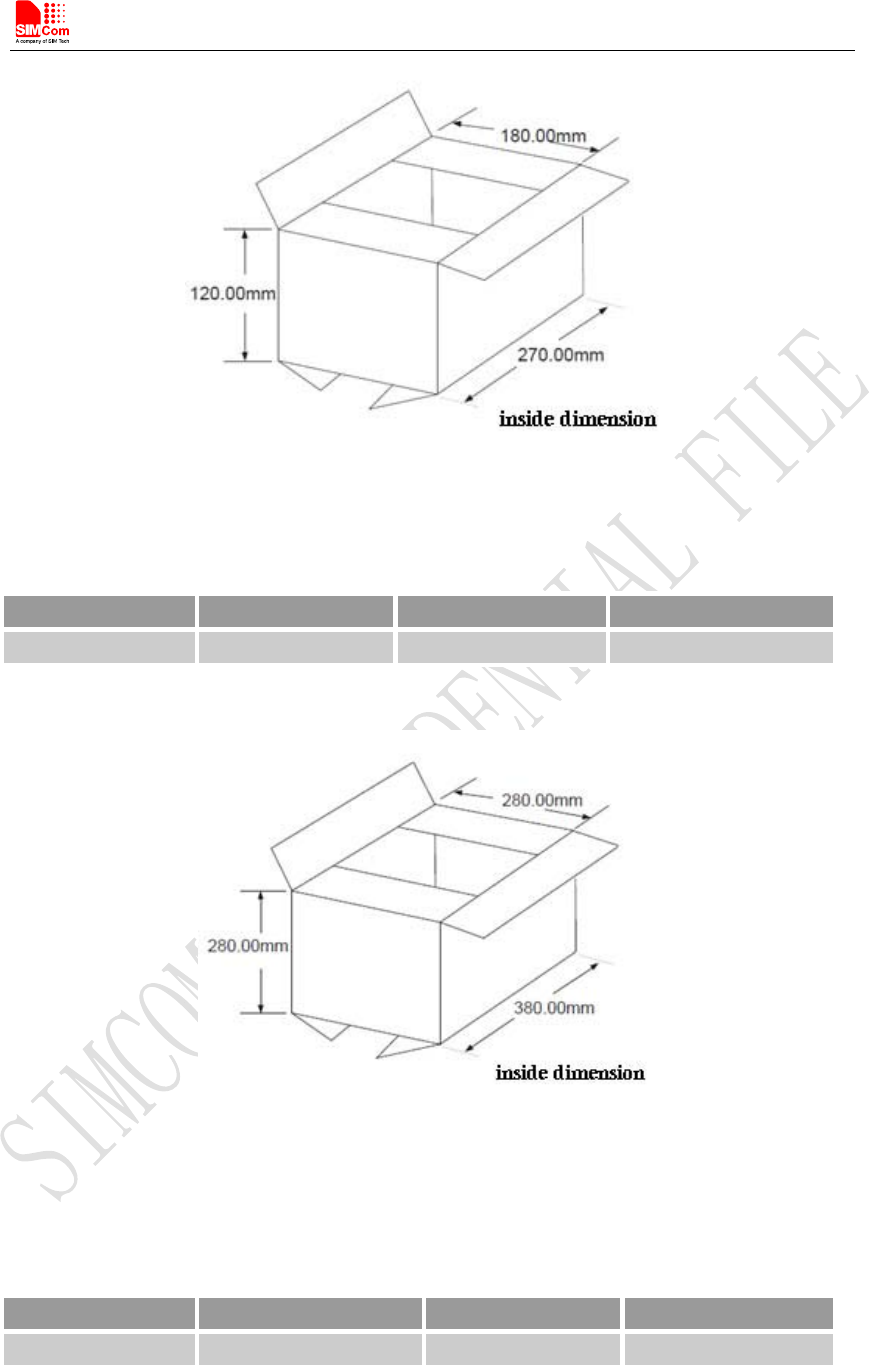
Figure 36: Small carton drawing introduce
Table 37: Small Carton size
Length(±10mm) Width(±10mm) Height(±10mm) Module number
270 180 120 15*20=300
Big carton drawing:
Figure 37: Big carton drawing introduce
Table 38: Big carton size
Length(±10mm) Width(±10mm) Height(±10mm)Module number
380 280 280 300*4=1200
Smart Machine Smart Decision
SIM7600A_User Manual_V1.01 2017-10-10
52
Appendix
A. Reference Design
Figure 38: Reference design
Note: The UART port suggest to be used by isolated circuit .
Smart Machine Smart Decision
SIM7600A_User Manual_V1.01 2017-10-10
53
B. Coding Schemes and Maximum Net Data Rates over Air Interface
Table 39: Coding schemes and maximum net data rates over air interface
Multislot definition(GPRS/EDGE)
Slot class DL slot number UL slot number Active slot number
1 1 1 2
2 2 1 3
3 2 2 3
4 3 1 4
5 2 2 4
6 3 2 4
7 3 3 4
8 4 1 5
9 3 2 5
10 4 2 5
11 4 3 5
12 4 4 5
GPRS coding scheme Max data rata(4 slots) Modulation type
CS 1 = 9.05 kb/s / time slot 36.2 kb/s GMSK
CS 2 = 13.4 kb/s / time slot 53.6 kb/s GMSK
CS 3 = 15.6 kb/s / time slot 62.4 kb/s GMSK
CS 4 = 21.4 kb/s / time slot 85.6 kb/s GMSK
EDGE coding scheme Max data rata(4 slots) Modulation type
MCS 1 = 8.8 kb/s/ time slot 35.2 kb/s GMSK
MCS 2 = 11.2 kb/s/ time slot 44.8 kb/s GMSK
MCS 3 = 14.8 kb/s/ time slot 59.2 kb/s GMSK
MCS 4 = 17.6 kb/s/ time slot 70.4 kb/s GMSK
MCS 5 = 22.4 kb/s/ time slot 89.6 kb/s 8PSK
MCS 6 = 29.6 kb/s/ time slot 118.4 kb/s 8PSK
MCS 7 = 44.8 kb/s/ time slot 179.2 kb/s 8PSK
MCS 8 = 54.4 kb/s/ time slot 217.6 kb/s 8PSK
MCS 9 = 59.2 kb/s/ time slot 236.8 kb/s 8PSK
HSDPA device category Max data rate(peak) Modulation type
Category 1 1.2Mbps 16QAM,QPSK
Category 2 1.2Mbps 16QAM,QPSK
Category 3 1.8Mbps 16QAM,QPSK
Category 4 1.8Mbps 16QAM,QPSK
Category 5 3.6Mbps 16QAM,QPSK
Category 6 3.6Mbps 16QAM,QPSK
Category 7 7.2Mbps 16QAM,QPSK
Category 8 7.2Mbps 16QAM,QPSK
Smart Machine Smart Decision
SIM7600A_User Manual_V1.01 2017-10-10
54
Category 9 10.2Mbps 16QAM,QPSK
Category 10 14.4Mbps 16QAM,QPSK
Category 11 0.9Mbps QPSK
Category 12 1.8Mbps QPSK
Category 13 17.6Mbps 64QAM
Category 14 21.1Mbps 64QAM
Category 15 23.4Mbps 16QAM
Category 16 28Mbps 16QAM
Category 17 23.4Mbps 64QAM
Category 18 28Mbps 64QAM
Category 19 35.5Mbps 64QAM
Category 20 42Mbps 64QAM
Category 21 23.4Mbps 16QAM
Category 22 28Mbps 16QAM
Category 23 35.5Mbps 64QAM
Category 24 42.2Mbps 64QAM
HSUPA device category Max data rate(peak) Modulation type
Category 1 0.96Mbps QPSK
Category 2 1.92Mbps QPSK
Category 3 1.92Mbps QPSK
Category 4 3.84Mbps QPSK
Category 5 3.84Mbps QPSK
Category 6 5.76Mbps QPSK
LTE-FDD device category
(Downlink) Max data rate(peak) Modulation type
Category 1 10Mbps QPSK/16QAM/64QAM
Category 2 50Mbps QPSK/16QAM/64QAM
Category 3 100Mbps QPSK/16QAM/64QAM
Category 4 150Mbps QPSK/16QAM/64QAM
LTE-FDD device category
(Uplink) Max data rate(peak) Modulation type
Category 1 5Mbps QPSK/16QAM
Category 2 25Mbps QPSK/16QAM
Category 3 50Mbps QPSK/16QAM
Category 4 50Mbps QPSK/16QAM
Smart Machine Smart Decision
SIM7600A_User Manual_V1.01 2017-10-10
55
C. Related Documents
Table 40: Related documents
SN Title Description
[1] SIM7X00 Series_AT
Command Manual_V1.xx SIM7X00 Series_AT Command Manual
[2] ITU-T Draft new
recommendationV.25ter Serial asynchronous automatic dialing and control
[3] GSM 07.07 Digital cellular telecommunications (Phase 2+); AT command
set for GSM Mobile Equipment (ME)
[4] GSM 07.10 Support GSM 07.10 multiplexing protocol
[5] GSM 07.05
Digital cellular telecommunications (Phase 2+); Use of Data
Terminal Equipment – Data Circuit terminating Equipment
(DTE – DCE) interface for Short Message Service (SMS)
and Cell Broadcast Service (CBS)
[6] GSM 11.14
Digital cellular telecommunications system (Phase 2+);
Specification of the SIM Application Toolkit for the
Subscriber Identity Module – Mobile Equipment (SIM – ME)
interface
[7] GSM 11.11
Digital cellular telecommunications system (Phase 2+);
Specification of the Subscriber Identity Module – Mobile
Equipment (SIM – ME) interface
[8] GSM 03.38 Digital cellular telecommunications system (Phase 2+);
Alphabets and language-specific information
[9] GSM 11.10
Digital cellular telecommunications system (Phase 2) ;
Mobile Station (MS) conformance specification; Part 1:
Conformance specification
[10] 3GPP TS 51.010-1 Digital cellular telecommunications system (Release 5);
Mobile Station (MS) conformance specification
[11] 3GPP TS 34.124 Electromagnetic Compatibility (EMC) for mobile terminals
and ancillary equipment.
[12] 3GPP TS 34.121 Electromagnetic Compatibility (EMC) for mobile terminals
and ancillary equipment.
[13] 3GPP TS 34.123-1
Technical Specification Group Radio Access Network;
Terminal conformance specification; Radio transmission and
reception (FDD)
[14] 3GPP TS 34.123-3 User Equipment (UE) conformance specification; Part 3:
Abstract Test Suites.
[15] EN 301 908-02 V2.2.1
Electromagnetic compatibility and Radio spectrum Matters
(ERM); Base Stations (BS) and User Equipment (UE) for
IMT-2000. Third Generation cellular networks; Part 2:
Harmonized EN for IMT-2000, CDMA Direct Spread
(UTRA FDD) (UE) covering essential requirements of article
3.2 of the R&TTE Directive
[16] EN 301 489-24 V1.2.1
Electromagnetic compatibility and Radio Spectrum Matters
(ERM); Electromagnetic Compatibility (EMC) standard for
radio equipment and services; Part 24: Specific conditions for
IMT-2000 CDMA Direct Spread (UTRA) for Mobile and
portable (UE) radio and ancillary equipment
[17] IEC/EN60950-1(2001) Safety of information technology equipment (2000)
[18] 3GPP TS 51.010-1 Digital cellular telecommunications system (Release 5);
Mobile Station (MS) conformance specification
Smart Machine Smart Decision
SIM7600A_User Manual_V1.01 2017-10-10
56
[19] GCF-CC V3.23.1 Global Certification Forum - Certification Criteria
[20] 2002/95/EC
Directive of the European Parliament and of the Council of
27 January 2003 on the restriction of the use of certain
hazardous substances in electrical and electronic equipment
(RoHS)
[21] Module
secondary-SMT-UGD-V1.xx
Module secondary SMT Guidelines
[22] SIM7X00
Series_UART_Application
Note_V1.xx
SIM7X00 Series_UART_Application Note
[23]
SIM7X00 Series_USB
AUDIO_Application
Note_V1.xx
SIM7X00 Series_USB AUDIO_Application Note
[24] Antenna design guidelines for
diversity receiver system
Antenna design guidelines for diversity receiver system
[25] SIM7X00 Series_Sleep Mode_
Application Note_V1.xx
SIM7X00 Series_Sleep Mode_ Application Note

Smart Machine Smart Decision
SIM7600A_User Manual_V1.01 2017-10-10
57
D. Terms and Abbreviations
Table 41: Terms and Abbreviations
Abbreviation Description
ADC Analog-to-Digital Converter
ARP Antenna Reference Point
BER Bit Error Rate
BTS Base Transceiver Station
CS Coding Scheme
CSD Circuit Switched Data
CTS Clear to Send
DAC Digital-to-Analog Converter
DRX Discontinuous Reception
DSP Digital Signal Processor
DTE Data Terminal Equipment (typically computer, terminal, printer)
DTR Data Terminal Ready
DTX Discontinuous Transmission
EFR Enhanced Full Rate
EGSM Enhanced GSM
EMC Electromagnetic Compatibility
ESD Electrostatic Discharge
ETS European Telecommunication Standard
EVDO Evolution Data Only
FCC Federal Communications Commission (U.S.)
FD SIM fix dialing phonebook
FDMA Frequency Division Multiple Access
FR Full Rate
GMSK Gaussian Minimum Shift Keying
GPRS General Packet Radio Service
GSM Global Standard for Mobile Communications
GNSS Global Navigation Satellite System
HR Half Rate
HSPA High Speed Packet Access
I2C Inter-Integrated Circuit
IMEI International Mobile Equipment Identity
LTE Long Term Evolution
MO Mobile Originated
MS Mobile Station (GSM engine), also referred to as TE
MT Mobile Terminated
PAP Password Authentication Protocol
PBCCH Packet Switched Broadcast Control Channel
PCB Printed Circuit Board
PCS Personal Communication System, also referred to as GSM 1900
RF Radio Frequency
RMS Root Mean Square (value)
RTC Real Time Clock
SIM Subscriber Identification Module
Smart Machine Smart Decision
SIM7600A_User Manual_V1.01 2017-10-10
58
SMS Short Message Service
SPI serial peripheral interface
SMPS Switched-mode power supply
TDMA Time Division Multiple Access
TE Terminal Equipment, also referred to as DTE
TX Transmit Direction
UART Universal Asynchronous Receiver & Transmitter
VSWR Voltage Standing Wave Ratio
SM SIM phonebook
NC Not connect
EDGE Enhanced data rates for GSM evolution
HSDPA High Speed Downlink Packet Access
HSUPA High Speed Uplink Packet Access
ZIF Zero intermediate frequency
WCDMA Wideband Code Division Multiple Access
VCTCXO Voltage control temperature-compensated crystal oscillator
USIM Universal subscriber identity module
UMTS Universal mobile telecommunications system
UART Universal asynchronous receiver transmitter
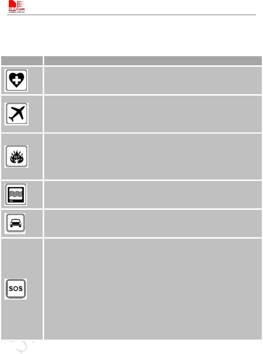
Smart Machine Smart Decision
SIM7600A_User Manual_V1.01 2017-10-10
59
E. Safety Caution
Table 42: Safety caution
Marks Requirements
When in a hospital or other health care facility, observe the restrictions about the use
of mobiles. Switch the cellular terminal or mobile off, medical equipment may be
sensitive and not operate normally due to RF energy interference.
Switch off the cellular terminal or mobile before boarding an aircraft. Make sure it is
switched off. The operation of wireless appliances in an aircraft is forbidden to
prevent interference with communication systems. Forgeting to think much of these
instructions may impact the flight safety or offend local legal action, or both.
Do not operate the cellular terminal or mobile in the presence of flammable gases or
fumes. Switch off the cellular terminal when you are near petrol stations, fuel depots,
chemical plants or where blasting operations are in progress. Operation of any
electrical equipment in potentially explosive atmospheres can constitute a safety
hazard.
Your cellular terminal or mobile receives and transmits radio frequency energy while
switched on. RF interference can occur if it is used close to TV sets, radios,
computers or other electric equipment.
Road safety comes first! Do not use a hand-held cellular terminal or mobile when
driving a vehicle, unless it is securely mounted in a holder for hands free operation.
Before making a call with a hand-held terminal or mobile, park the vehicle.
GSM cellular terminals or mobiles operate over radio frequency signals and cellular
networks and cannot be guaranteed to connect in all conditions, especially with a
mobile fee or an invalid SIM card. While you are in this condition and need emergent
help, please remember to use emergency calls. In order to make or receive calls, the
cellular terminal or mobile must be switched on and in a service area with adequate
cellular signal strength.
Some networks do not allow for emergency call if certain network services or phone
features are in use (e.g. lock functions, fixed dialing etc.). You may have to
deactivate those features before you can make an emergency call.
Also, some networks require that a valid SIM card be properly inserted in the cellular
terminal or mobile.

Smart Machine Smart Decision
SIM7600A_User Manual_V1.01 2017-10-10
60
Contact us:
Shanghai SIMCom Wireless Solutions Ltd.
Add: SIM Technology Building, No.633, Jinzhong Road, Changning District, Shanghai P.R. China
200335
Tel:+86 21 3235 3300
Fax:+86 21 3235 3020
URL:www.simcomm2m.com