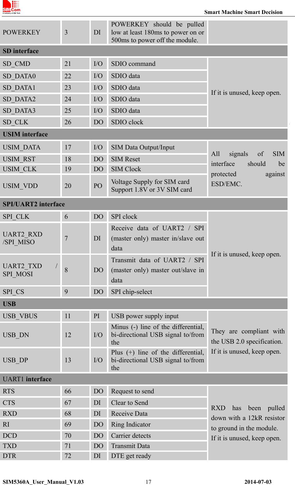
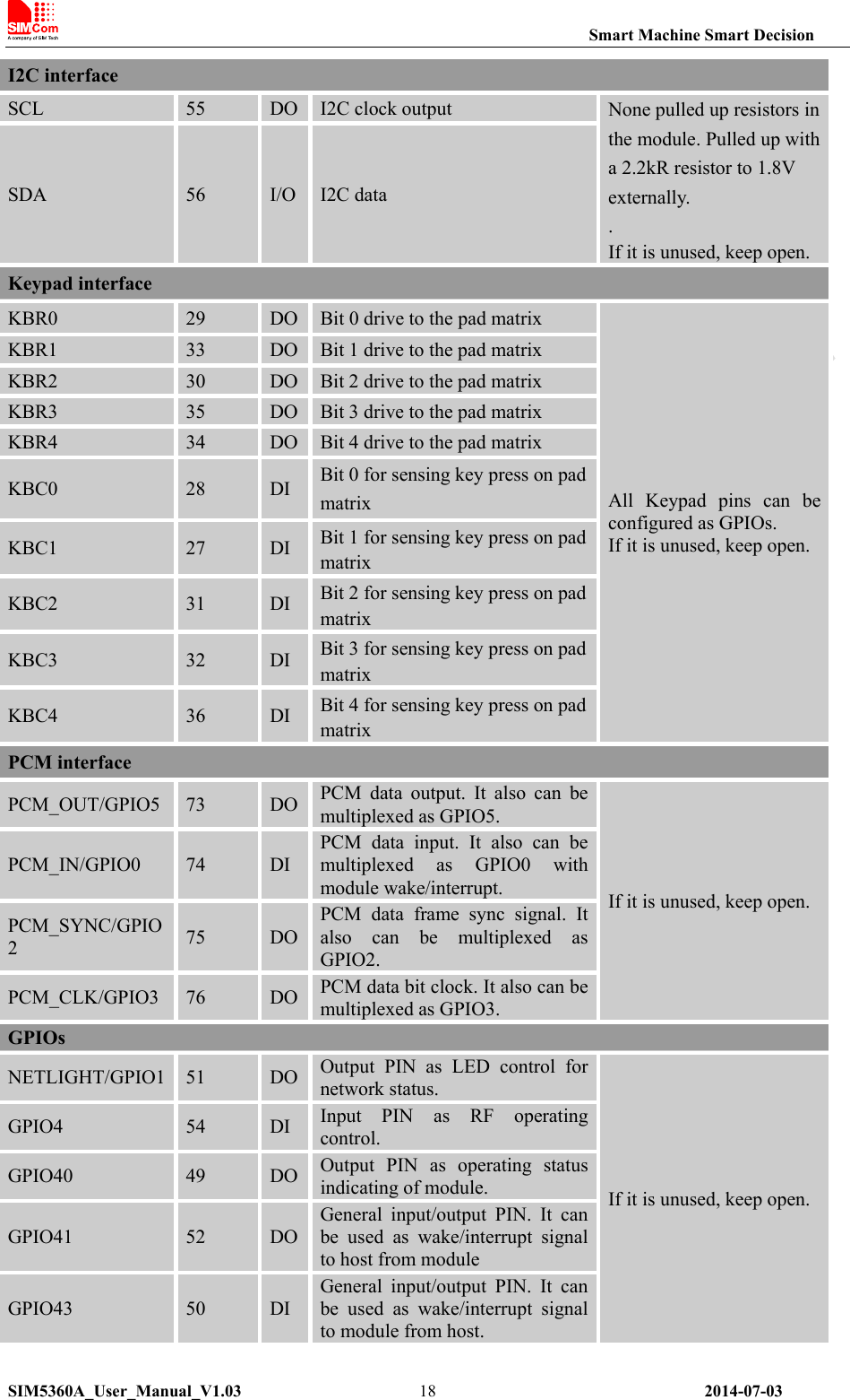
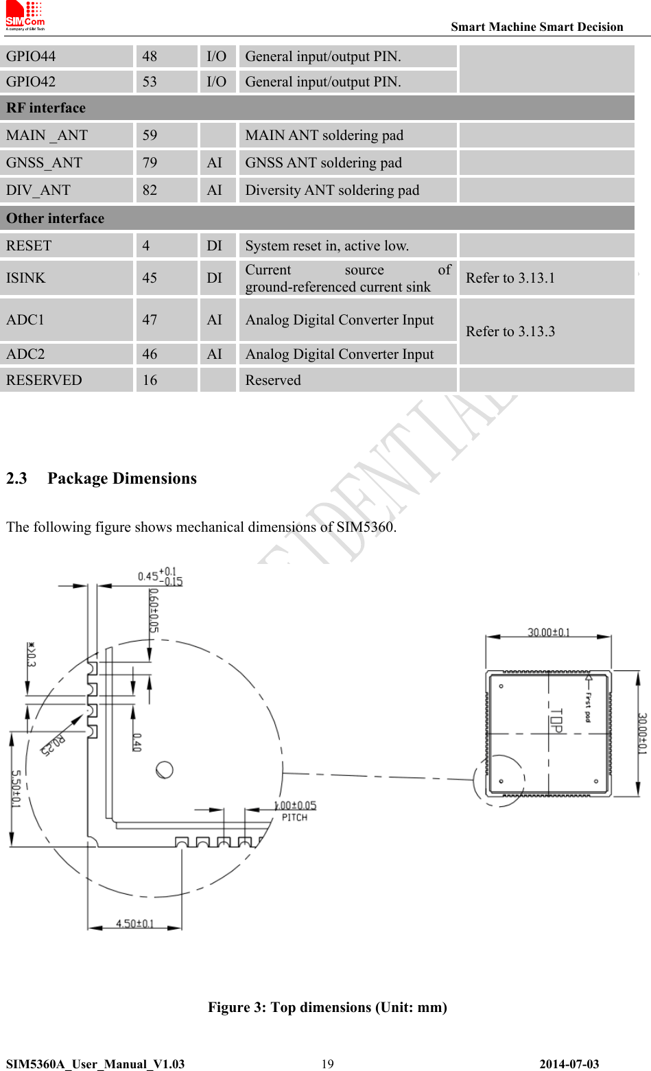
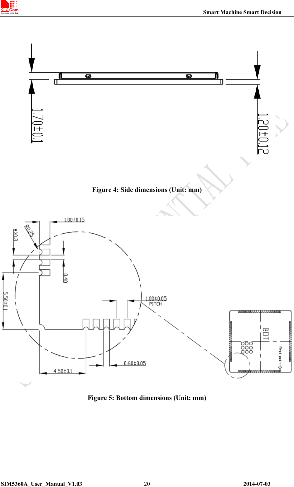
Simcom SIM5360A GSM/WCDMA Module User Manual SIM5360A Rev 1
Shanghai Simcom Ltd. GSM/WCDMA Module SIM5360A Rev 1
UserManual.wiki
>
Simcom
>
SIM5360A User Manual
>
SIM5360A_User Manual_Rev 1
Contents
1.
SIM5360A_EVB User Guide_Rev 1
2.
SIM5360A_User Manual_Rev 1
SIM5360A_User Manual_Rev 1
Navigation menu
Upload a User Manual
Namespaces
Wiki Guide
HTML
PDF
Info
Views
User Manual
Discussion / Help
Navigation
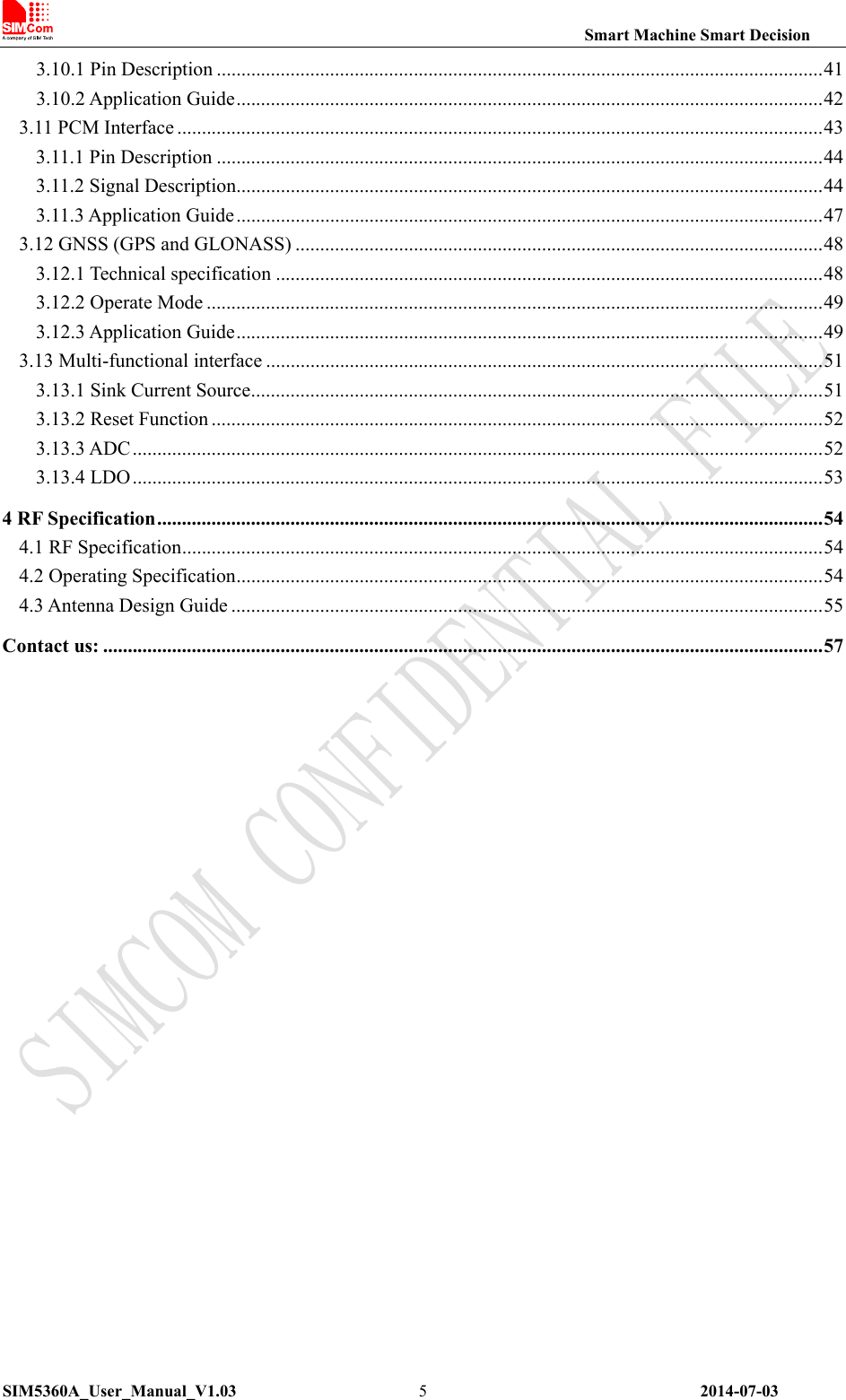
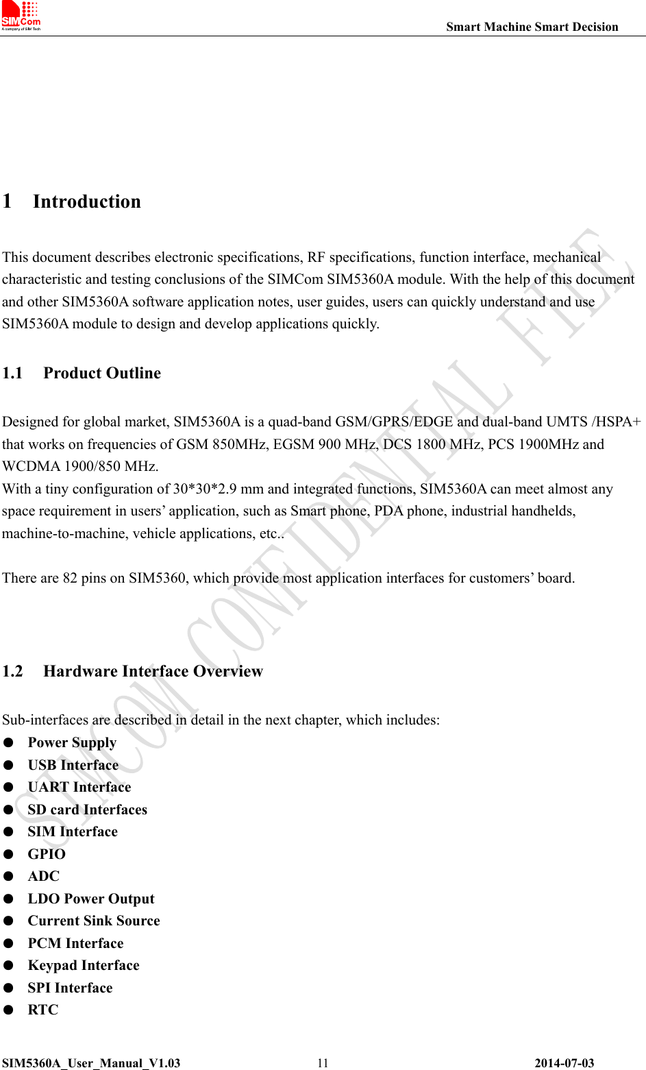
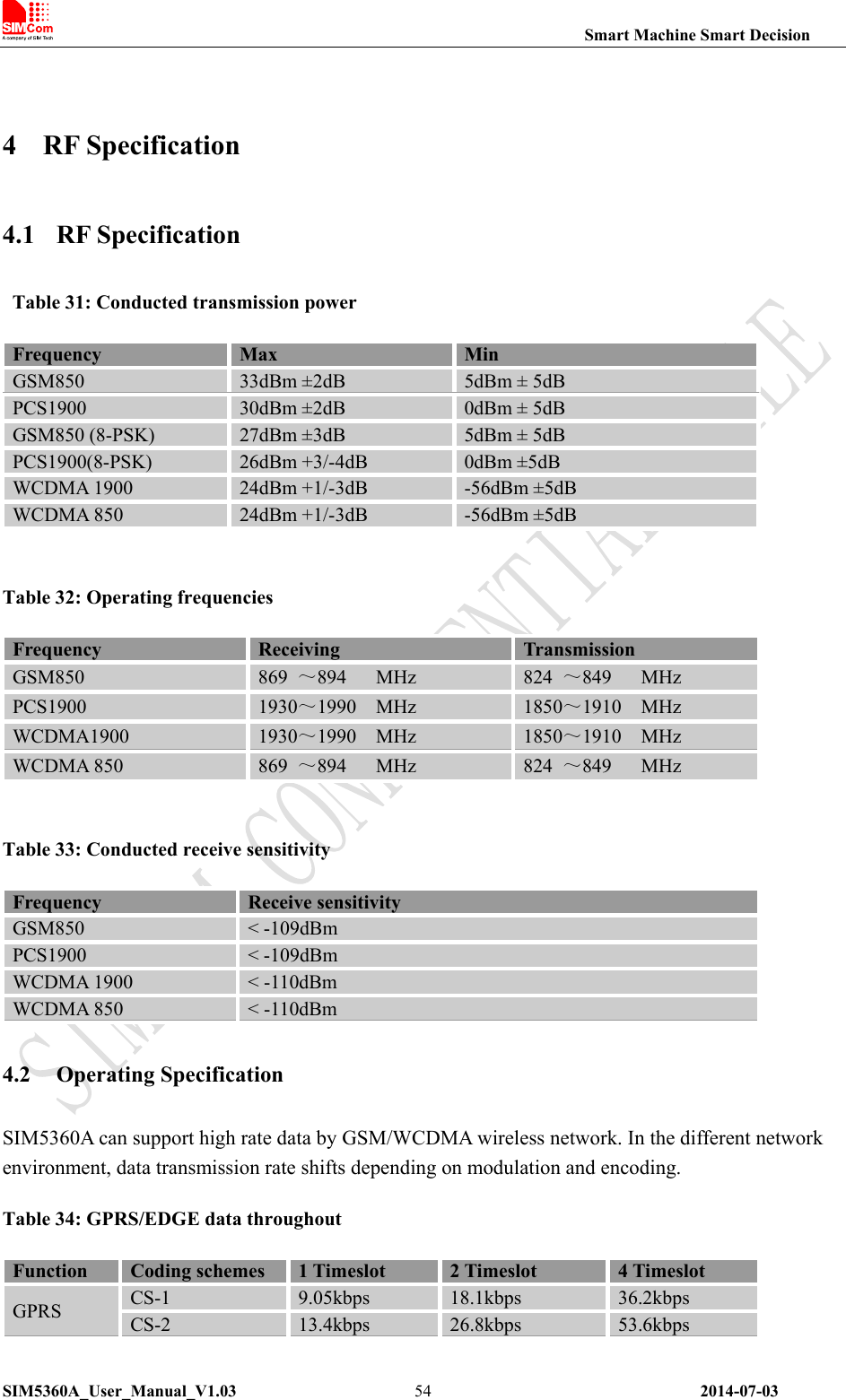
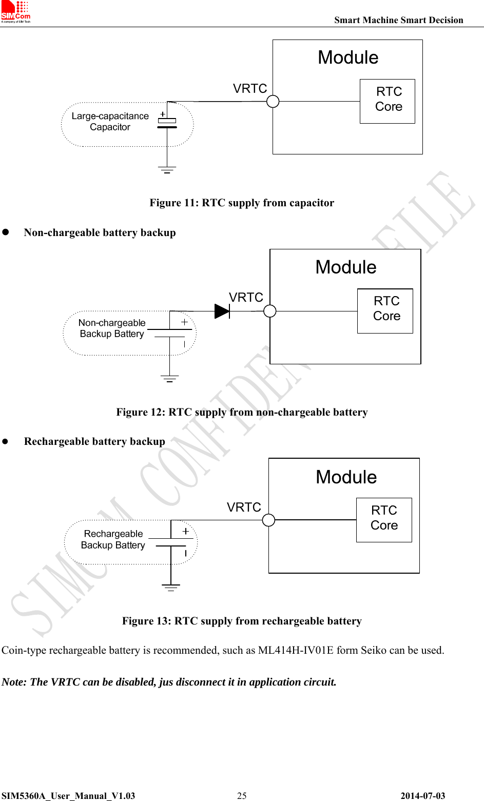
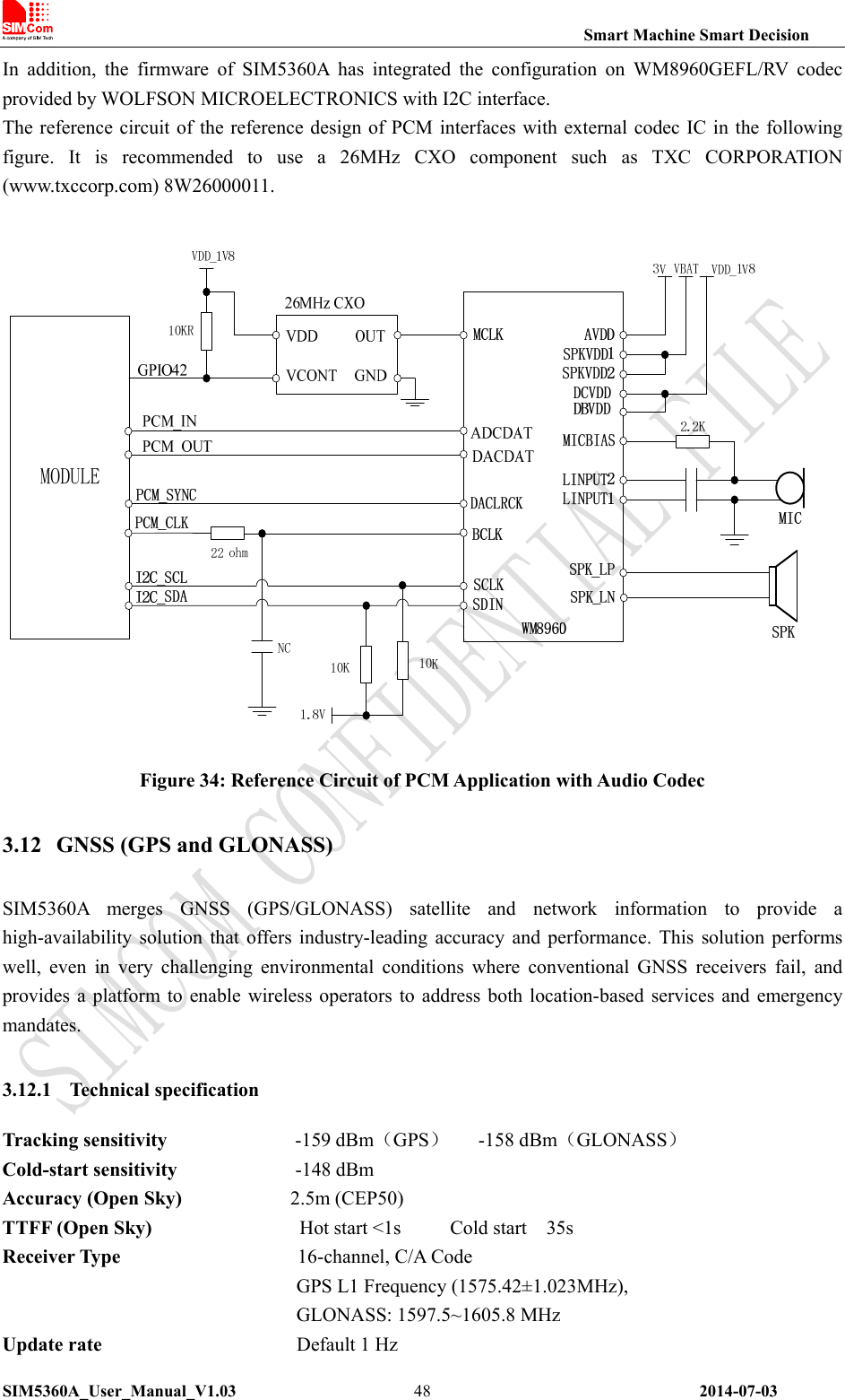
![Smart Machine Smart Decision SIM5360A_User_Manual_V1.03 2014-07-03 24power will be preferable because of its better efficiency, especially at the high current situation. The following figure is the reference circuit. Note that DCDC may deprave RF performance because of ripple current intrinsically. Figure 10: Reference circuit of the DCDC power supply Volta ge monito r To monitor the power supply voltage, user can use the AT command “AT+CBC”, this command has two parameters: the battery status and the voltage value (mV). It will return the capacity percentage and actual value of battery (at the VBAT pin). The voltage is continuously measured at intervals, whenever the measured battery voltage is lower than a specific value set by the AT command “AT+CVALARM”. For example, if the voltage value is set to be 3.4V, the following URC will be presented: “warning! voltage is low: 3.3v”. If the voltage is lower than a specific value which is set by the AT command “AT+CPMVT”, the module will be powered off automatically and AT commands cannot be executed any more. Note: Under-voltage warning function is disabled by default, user can enable it by the AT command “AT+CVALARM”. Please refer to Document [1]. 3.1.3 RTC Backup The module uses RTC (Real Time Clock) to update and maintain inherent time and keeps system alive at no power supply status. The RTC power supply of module can be provided by an external capacitor or a battery (non-chargeable or rechargeable) through the VRTC. The following figures show various reference circuits for RTC back up. The discharge current is less than 10uA. External capacitor backup](https://usermanual.wiki/Simcom/SIM5360A.SIM5360A-User-Manual-Rev-1/User-Guide-2350109-Page-24.png)
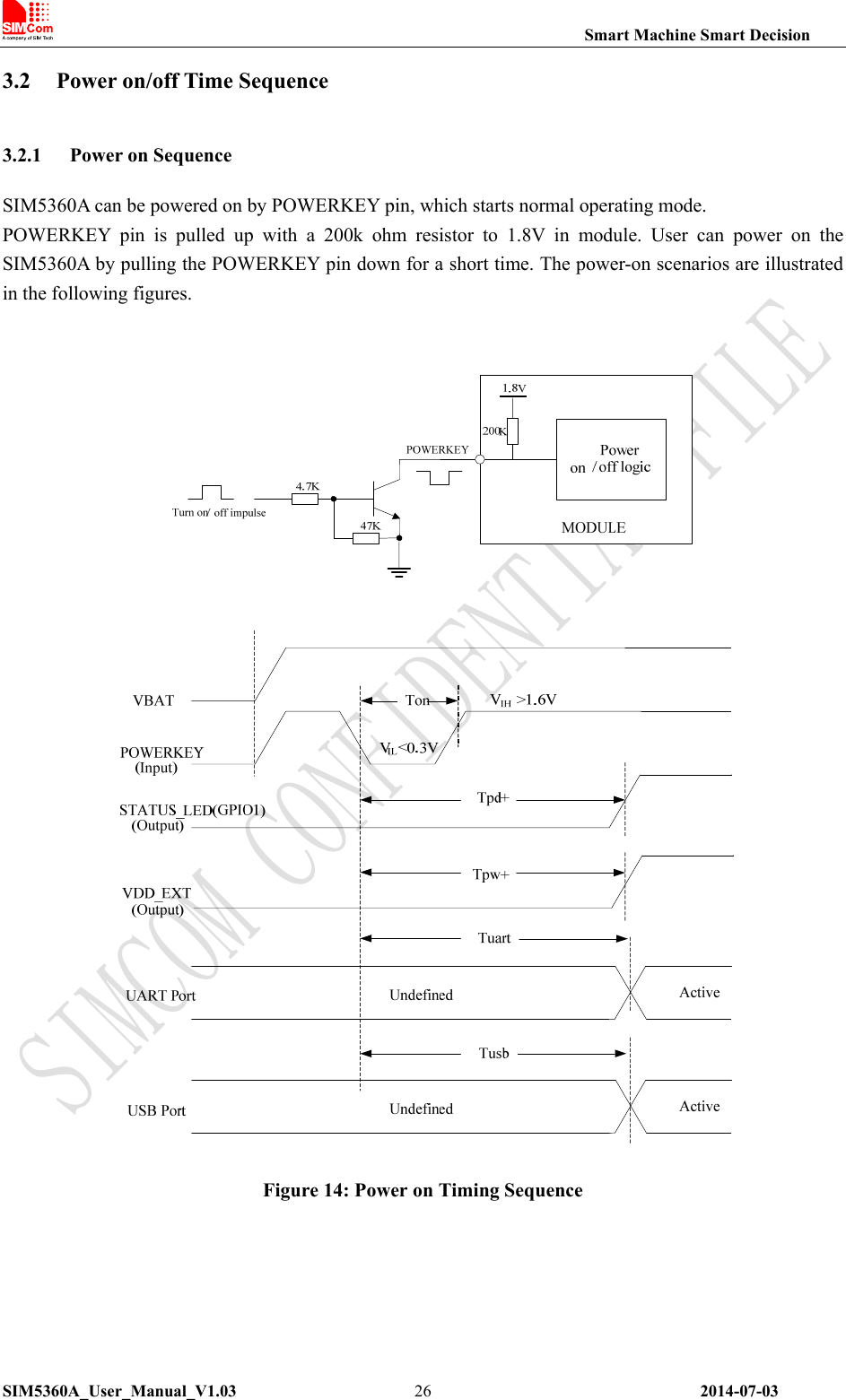
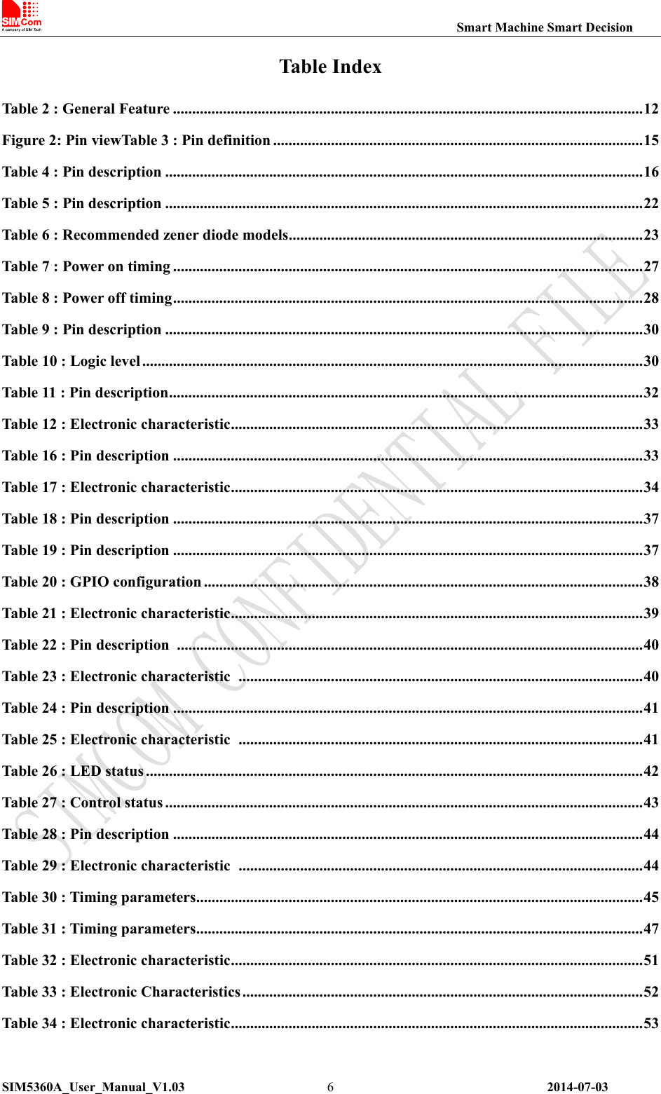
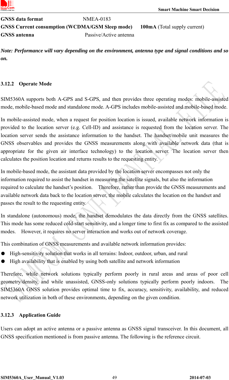
![Smart Machine Smart Decision SIM5360A_User_Manual_V1.03 2014-07-03 27Table 6: Power on timing Symbol Parameter Time value UnitMin. Typ. Max. Ton The time to pull POWERKEY down to power on 180 500 - ms TpD+ The time to indicate connecting with the network - - 5 s Tpw+ The time to indicate the module is powered on completely - - 0.5 s Tuart The time to enable UART - - 8 s Tusb The time to enable USB - - 10 s Note: Module could be automatically power on by connecting Power ON pin to Low level directly. Before designing, please refer to Document [27] for more detail. 3.2.2 Power off Sequence The following methods can be used to power down SIM5360. These procedures will make module disconnect from the network and allow the software to enter a safe state, and then save data before completely powering the module off. ● Method 1: Power off SIM5360A by pulling the POWERKEY pin down ● Method 2: Power off SIM5360A by AT command User can power off the SIM5360A by pulling POWERKEY down for a specific time. The power off scenario is illustrated in the following figure.](https://usermanual.wiki/Simcom/SIM5360A.SIM5360A-User-Manual-Rev-1/User-Guide-2350109-Page-27.png)
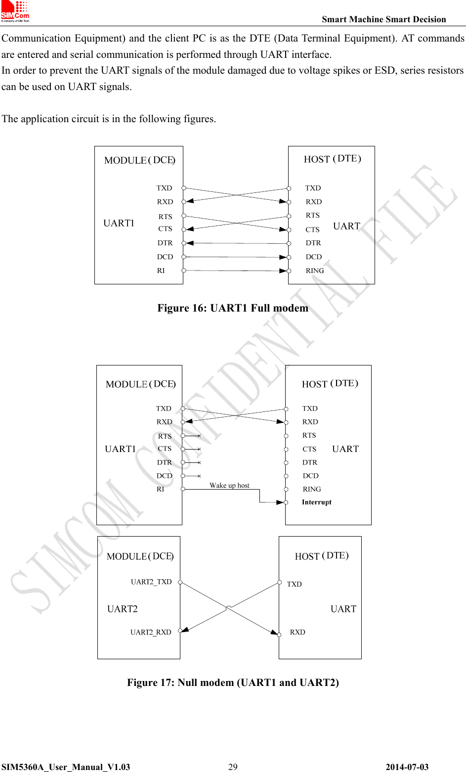
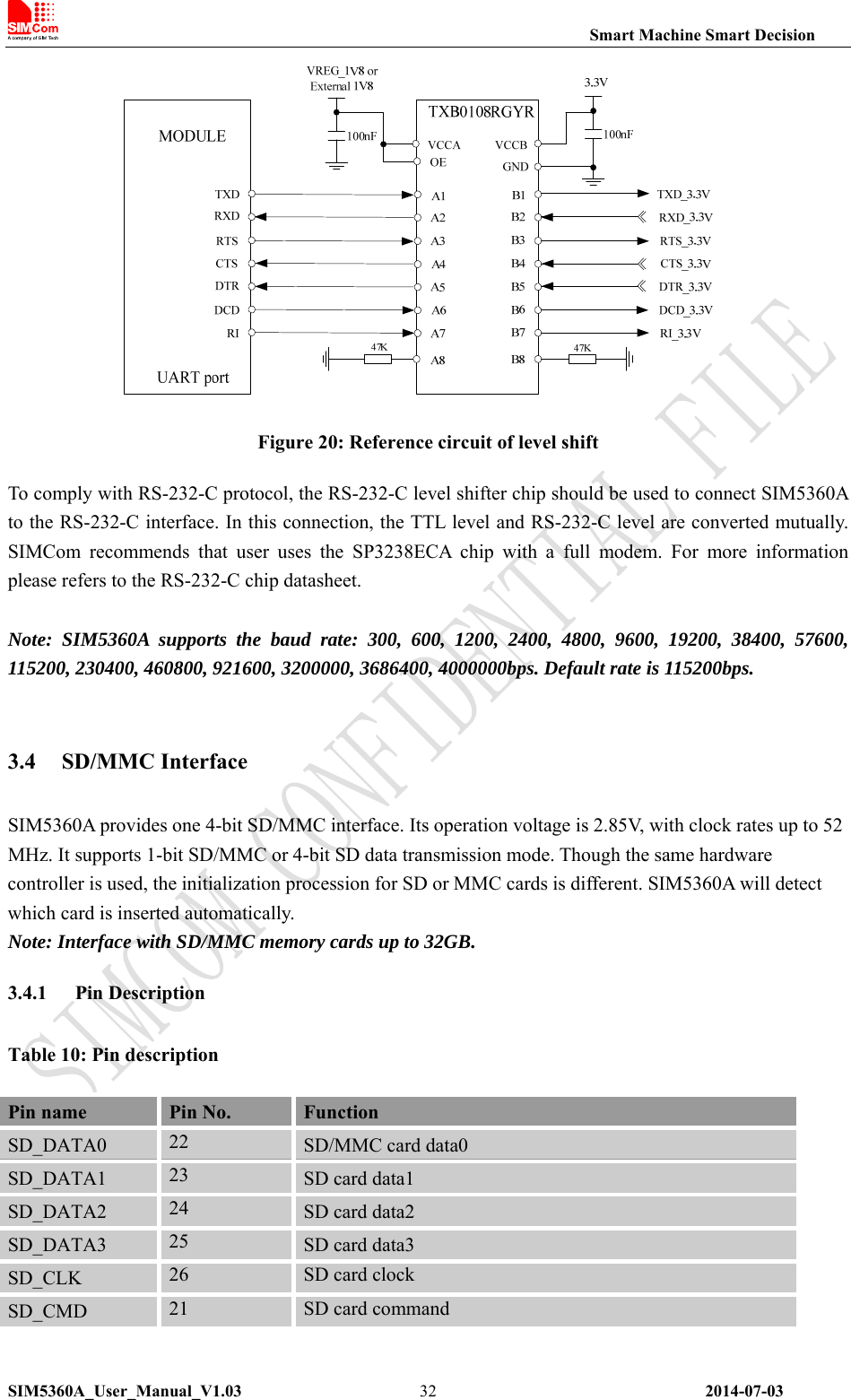
![Smart Machine Smart Decision SIM5360A_User_Manual_V1.03 2014-07-03 28 Figure 15: Power off timing sequence Table 7: Power off timing Symbol Parameter Time value Min. Typ. Max. Unit Toff The time pulling POWERKEY down to power off 0.5 - 5 s TpD- The time to indicate disconnecting from the network - - 2 s Tpw- The time to indicate the module power off completely - - 2 s Tuart The time to disable UART - - 3 s Tusb The time to disable USB - - 2 s Trestart The time to power on again after Tpw- 0 - - s User can also use the AT command “AT+CP OF ” to power down the module. After that, the AT commands cannot be executed any longer. The module enters the POWER DOWN mode, only the RTC is still active. For details, refer to Document [1]. 3.3 UART Interface SIM5360A provides two UARTs (universal asynchronous serial transmission) port. UART1 consists of a flexible 7-wire serial interface. UART2 consists of 2-wire serial interface. The module is as the DCE (Data](https://usermanual.wiki/Simcom/SIM5360A.SIM5360A-User-Manual-Rev-1/User-Guide-2350109-Page-28.png)
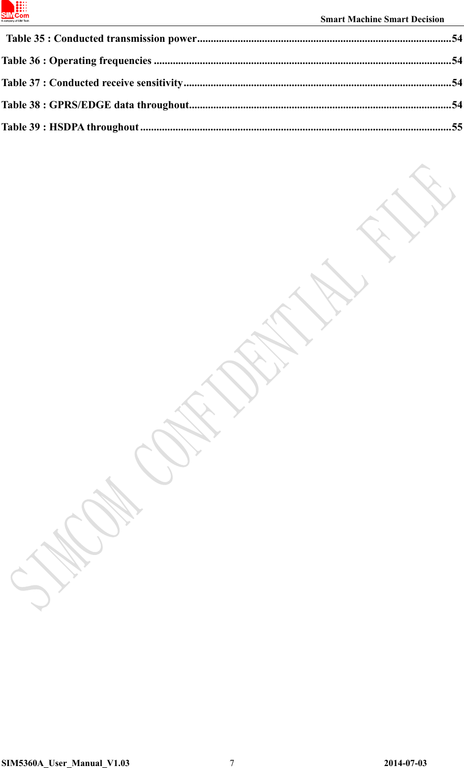
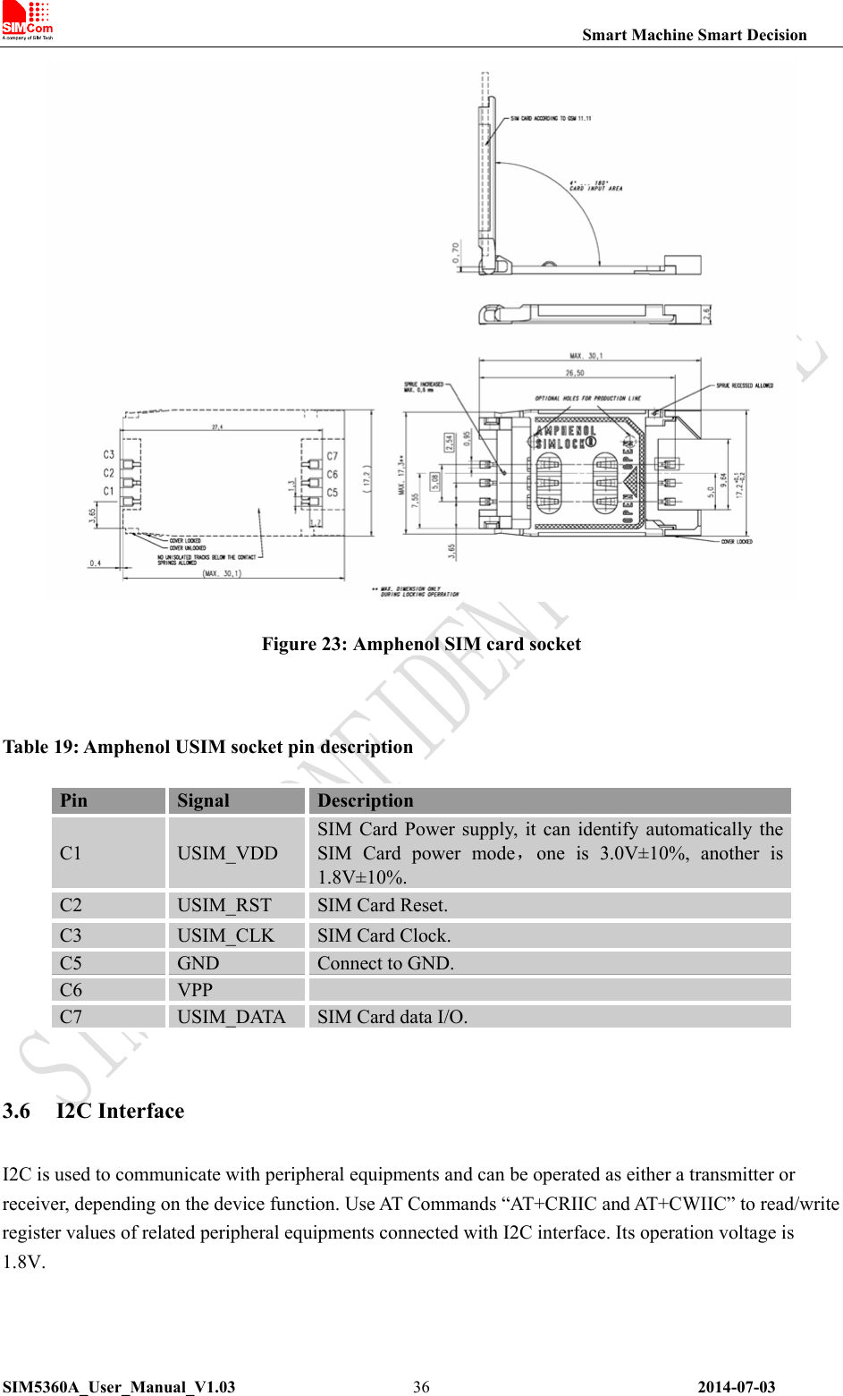
![Smart Machine Smart Decision SIM5360A_User_Manual_V1.03 2014-07-03 35 Figure 22: USIM interface reference circuit Note: USIM_DATA has been pulled up with a 15kohm resistor to USIM_VDD in module. A 220nF shut capacitor on USIM_VDD is used to reduce interference. Use AT Commands to get information in USIM card. For more detail, please refer to document [1]. 3.5.3 Recommend Components For 6 pins USIM socket, SIMCom recommend to use Amphenol C707 10M006 512 2. User can visit http://www.amphenol.com for more information about the holder.](https://usermanual.wiki/Simcom/SIM5360A.SIM5360A-User-Manual-Rev-1/User-Guide-2350109-Page-35.png)
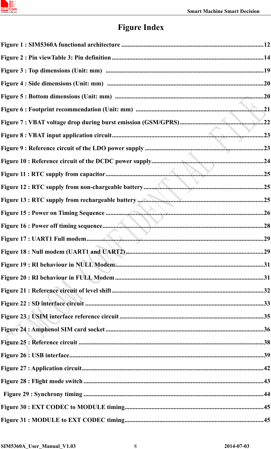
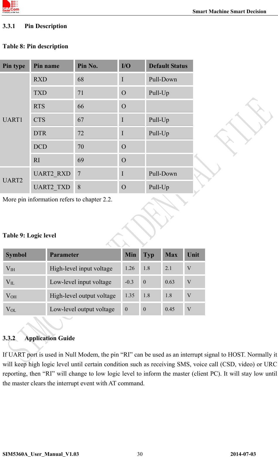
![Smart Machine Smart Decision SIM5360A_User_Manual_V1.03 2014-07-03 39KBC4 GPIO11 KBC3 GPIO12 KBC2 GPIO13 KBC1 GPIO14 KBC0 GPIO15 Note: Refer to document [23] for detailed information of Keypad Application Note. 3.8 USB Interface SIM5360A module contains a USB interface. This interface is compliant with the USB2.0 specification. The USB2.0 specification requires hosts such as the computer to support all three USB speeds, namely low-speed (1.5Mbps), full-speed (12Mbps) and high-speed (480Mbps). USB charging and USB-OTG is not supported. Table 17: Electronic characteristic Pin name Pin No. Input voltage scope( V ) Min Typ Max USB_VBUS 11 3 5.0 5.25 USB_DP 13 They are compliant with the USB 2.0 specification. USB_DN 12 3.8.1 Application Guide Currently SIM5360A supports the USB suspend and resume mechanism which can help to save power. If no transaction is on USB bus, SIM5360A will enter suspend mode. When some events such as voice call or receiving SMS happen, SIM5360A will resume normal mode automatically. Figure 25: USB interface](https://usermanual.wiki/Simcom/SIM5360A.SIM5360A-User-Manual-Rev-1/User-Guide-2350109-Page-39.png)
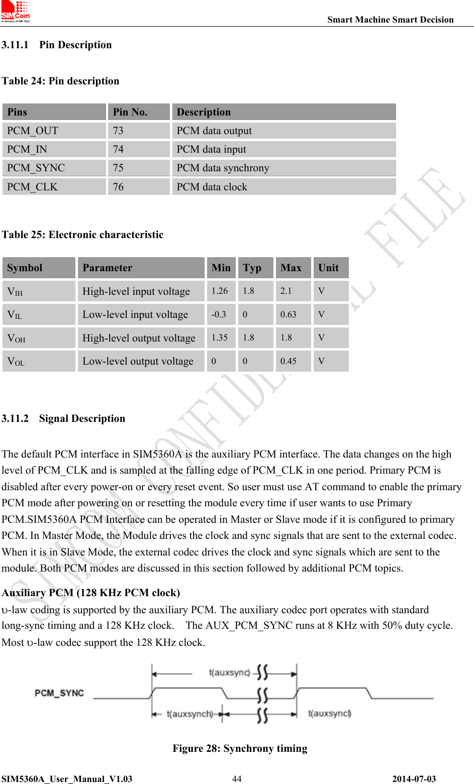
![Smart Machine Smart Decision SIM5360A_User_Manual_V1.03 2014-07-03 43 Figure 27: Flight mode switch Table 23: Control status GPIO4 Status Module operation Low Level Flight Mode: RF is closed. High Level Normal Mode: RF is working. Note:1. For SIM5360, GPIO0, GPIO2, GPIO3 and GPIO5 have multiplex function, user can use them as PCM interface to connect extend codec. Refer to section 3.11 and document [1] for details. 2. When the module is powered off, make sure all digital interfaces (PCM UART, etc) connected with peripheral devices have no voltage higher than 0.3V. If users’ design cannot meet above conditions, high level voltages maybe occur in GPIO pins because current leakage from above digital interfaces may occur. 3.11 PCM Interface SIM5360A provides hardware PCM interface for external codec. The PCM interface enables communication with an external codec to support hands-free applications. SIM5360A PCM interface can be used in two modes: the default mode is auxiliary PCM (8 KHz long sync mode at 128 KHz PCM CLK); the other mode is primary PCM (8 KHz short sync mode at 2048 KHz PCM CLK). In short-sync (primary PCM) mode, SIM5360A can be a master or a slave. In long-sync (auxiliary PCM) mode, SIM5360A is always a master. SIM5360A also supports 3 kinds of coding formats: 8 bits (-law or A-law) and 16 bits (linear). Note: PCM interface is multiplexed from GPIO (default setting). The AT command “AT+CPCM” is used to switch between PCM and GPIO functions. Please refer to document [21] and document [1] for details.](https://usermanual.wiki/Simcom/SIM5360A.SIM5360A-User-Manual-Rev-1/User-Guide-2350109-Page-43.png)
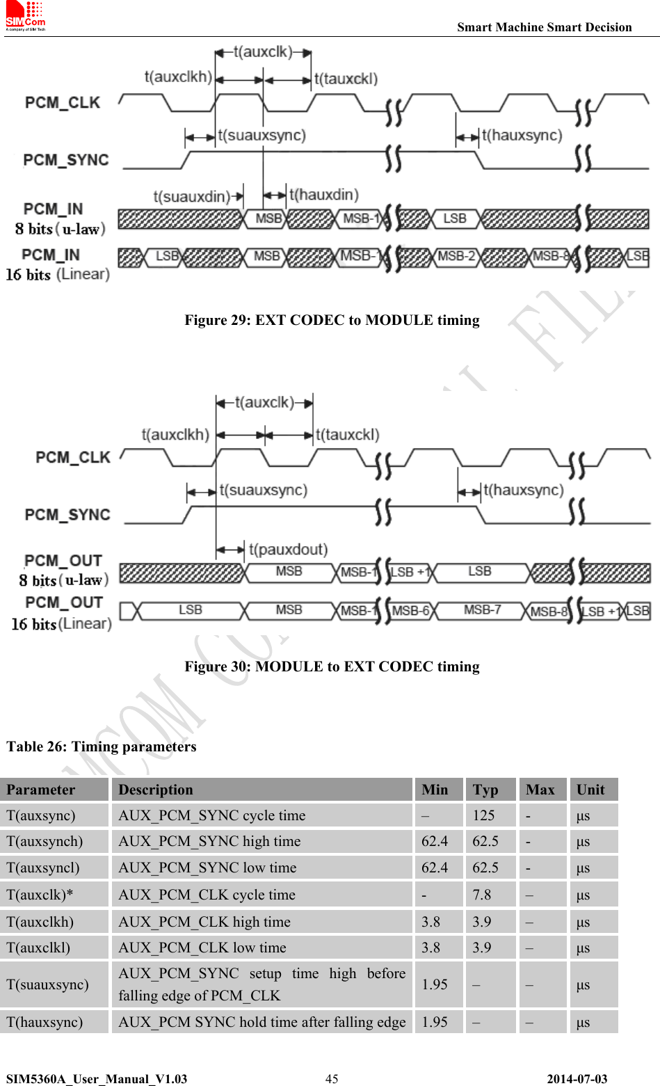
![Smart Machine Smart Decision SIM5360A_User_Manual_V1.03 2014-07-03 47 Figure 33: MODULE to EXT CODEC timing Table 27: Timing parameters Parameter Description Min Typ Max Unit T(sync) PCM_SYNC cycle time – 125 – μs T(synch) PCM_SYNC high time 400 500 – ns T(syncl) PCM_SYNC low time – 124.5 – μs T(clk) PCM_CLK cycle time – 488 – ns T(clkh) PCM_CLK high time – 244 – ns T(clkl) PCM_CLK low time – 244 – ns T(susync) PCM_SYNC setup time high before falling edge of PCM_CLK 60 – – ns T(hsync) PCM_SYNC hold time after falling edge of PCM_CLK 60 – – ns T(sudin) PCM_IN setup time before falling edge of PCM_CLK 50 – – ns T(hdin) PCM_IN hold time after falling edge of PCM_CLK 10 – – ns T(pdout) Delay from PCM_CLK rising to PCM_OUT valid – – 350 ns T(zdout) Delay from PCM_CLK falling to PCM_OUT HIGH-Z – 160 – ns Note: SIM5360A can transmit PCM data by USB except for PCM interface. 3.11.3 Application Guide The mode of SIM5360A PCM can be configured by AT command “AT+CPCM and AT+CPCMFMT”, and the default configuration is master mode using short sync data format with 2.048MHz PCM_CLK and 8 kHz PCM_SYNC. Please refer to document [21] and document [1] for details.](https://usermanual.wiki/Simcom/SIM5360A.SIM5360A-User-Manual-Rev-1/User-Guide-2350109-Page-47.png)
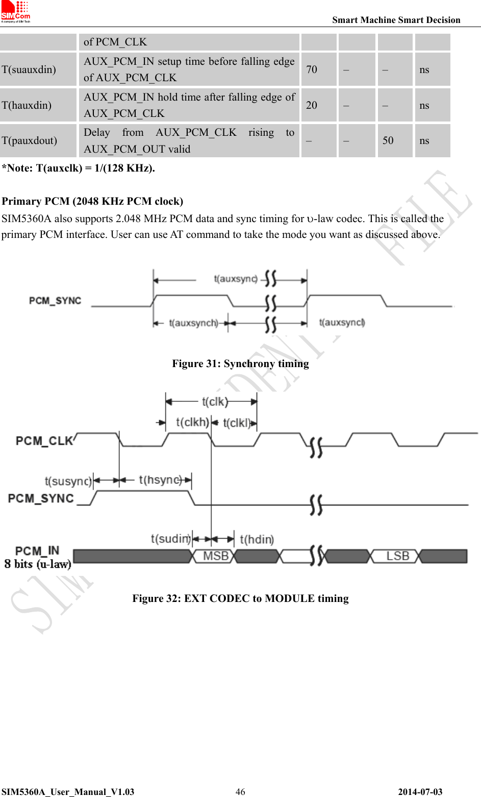
![Smart Machine Smart Decision SIM5360A_User_Manual_V1.03 2014-07-03 53data which is between 0 and 32768. The data can be transformed to any type such as voltage, temperature etc. Please refer to document [1]. Note: The input signal voltage value in ADC must not be higher than 2.2V. 3.13.4 LDO SIM5360A has a LDO power output, namely VDD_EXT. The LDO is available and output voltage is 2.85v by default, rated for 300mA. User can switch the LDO on or off by the AT command “AT+CVAUXS” and configure its output voltage by the AT command “AT+CVAUXV”. Table 30: Electronic characteristic Symbol Description Min Typ Max Unit VDD_EXT Output voltage 1.5 2.85 3.05 V IO Output current - - 300 mA](https://usermanual.wiki/Simcom/SIM5360A.SIM5360A-User-Manual-Rev-1/User-Guide-2350109-Page-53.png)