Simcom SIM5360A GSM/WCDMA Module User Manual SIM5360A Rev 1
Shanghai Simcom Ltd. GSM/WCDMA Module SIM5360A Rev 1
Simcom >
Contents
- 1. SIM5360A_EVB User Guide_Rev 1
- 2. SIM5360A_User Manual_Rev 1
SIM5360A_User Manual_Rev 1

SIM5360A_User_Manual_V1.03
Document Title SIM5360A User Manual
Version 1.03
Date 2014-07-03
Status Release
Document Control ID SIM5360A_User_Manual_V1.03

Smart Machine Smart Decision
Compliance Information
FCC Compliance Statement: This device complies with Part 15 of the FCC Rules . Operation is subject to
the following two conditions: 1. This device may not cause harmful interference, and 2. This device must
accept any interference received, including interference that may cause undesired operation. This device
must accept any interference received, including interference that may cause undesired operation. Product
that is a radio transmitter is labeled with FCC ID.
FCC Caution
(1)Exposure to Radio Frequency Radiation. This equipment must be installed and operated in accordance
with provided instructions and the antenna(s) used for this transmitter must be installed to provide a
separation distance of at least 20 cm from all persons and must not be collocated or operating in
conjunction with any other antenna or transmitter. End-users and installers must be provided with antenna
installation instructions and transmitter operating conditions for satisfying RF exposure compliance.
(2) Any changes or modifications not expressly approved by the grantee of this device could void the
user's authority to operate the equipment.
(3) This Transmitter must not be co-located or operating in conjunction with any other antenna or
transmitter.
(4) Changes or modifications to this unit not expressly approved by the party responsible for compliance
could void the user authority to operate the equipment.
(5) the modules FCC ID is not visible when installed in the host, or
(6) if the host is marketed so that end users do not have straight forward commonly used methods for
access to remove the module so that the FCC ID of the module is visible; then an additional permanent
label referring to the enclosed module: Contains Transmitter Module FCC ID: UDV-SIM5360A or
Contains FCC ID: UDV-SIM5360A must be used.
IC Notice
This device complies with Industry Canada license-exempt RSS standard(s). Operation is subject to the
following two conditions: this device may not cause interference, and this device must accept any
interference, including interference that may cause undesired operation of the device.
Le présent appareil est conforme aux CNR d'Industrie Canada applicables aux appareils radio exempts de
licence. L'exploitation est autorisée aux deux conditions suivantes: l'appareil ne doit pas produire de
brouillage, et l'utilisateur de l'appareil doit accepter tout brouillage radioélectrique subi, même si le
brouillage est susceptible d'en
This Class B digital apparatus complies with Canadian ICES-003.
Cet appareil numérique de la classe B est conforme à la norme NMB-003 du Canada.
General Notes
SIMCom offers this information as a service to its customers, to support application and engineering
efforts that use the products designed by SIMCom. The information provided is based upon requirements
specifically provided to SIMCom by the customers. SIMCom has not undertaken any independent search
for additional relevant information, including any information that may be in the customer’s possession.
Furthermore, system validation of this product designed by SIMCom within a larger electronic system
remains the responsibility of the customer or the customer’s system integrator. All specifications supplied
herein are subject to change.

Smart Machine Smart Decision
SIM5360A_User_Manual_V1.03 2014-07-03
3
Copyright
This document contains proprietary technical information which is the property of SIMCom Limited,
copying of this document and giving it to others and the using or communication of the contents thereof,
are forbidden without express authority. Offenders are liable to the payment of damages. All rights
reserved in the event of grant of a patent or the registration of a utility model or design. All specification
supplied herein are subject to change without notice at any time.
Copyright © Shanghai SIMCom Wireless Solutions Ltd. 2014

Smart Machine Smart Decision
SIM5360A_User_Manual_V1.03 2014-07-03
4
Contents
Revision History ......................................................................................................................................... 10
1 Introduction ............................................................................................................................................. 11
1.1 Product Outline ................................................................................................................................... 11
1.2 Hardware Interface Overview ............................................................................................................. 11
1.3 Hardware Diagram .............................................................................................................................. 12
1.4 Functional Overview ........................................................................................................................... 12
2 Package Information ............................................................................................................................... 13
2.1 Pin Configuration ................................................................................................................................ 13
2.2 Pin description .................................................................................................................................... 16
2.3 Package Dimensions ........................................................................................................................... 19
2.4 Footprint Recommendation ................................................................................................................. 21
3 Application Interface Specification ........................................................................................................ 21
3.1 Power Supply ...................................................................................................................................... 21
3.1.1 Power Supply Pin ......................................................................................................................... 22
3.1.2 Design Guide ................................................................................................................................ 22
3.1.3 RTC Backup ................................................................................................................................. 24
3.2 Power on/off Time Sequence .............................................................................................................. 26
3.2.1 Power on Sequence ....................................................................................................................... 26
3.2.2 Power off Sequence ...................................................................................................................... 27
3.3 UART Interface ................................................................................................................................... 28
3.3.1 Pin Description ............................................................................................................................. 30
3.3.2 Application Guide ......................................................................................................................... 30
3.4 SD/MMC Interface ............................................................................................................................. 32
3.4.1 Pin Description ............................................................................................................................. 32
3.4.2 Design guide ................................................................................................................................. 33
3.5 USIM Interface ................................................................................................................................... 33
3.5.1 Pin description .............................................................................................................................. 33
3.5.2 Application Guide ......................................................................................................................... 34
3.5.3 Recommend Components ............................................................................................................. 35
3.6 I2C Interface ....................................................................................................................................... 36
3.6.1 Pin Description ............................................................................................................................. 37
3.6.2 Signal Description ........................................................................................................................ 37
3.6.3 Design Guide ................................................................................................................................ 37
3.7 Keypad Interface ................................................................................................................................. 37
3.7.1 Pin Description ............................................................................................................................. 37
3.7.2 Application Guide ......................................................................................................................... 38
3.8 USB Interface ...................................................................................................................................... 39
3.8.1 Application Guide ......................................................................................................................... 39
3.9 SPI Interface ........................................................................................................................................ 40
3.9.1 Pin Description ............................................................................................................................. 40
3.10 GPIO Interface .................................................................................................................................. 40

Smart Machine Smart Decision
SIM5360A_User_Manual_V1.03 2014-07-03
5
3.10.1 Pin Description ........................................................................................................................... 41
3.10.2 Application Guide ....................................................................................................................... 42
3.11 PCM Interface ................................................................................................................................... 43
3.11.1 Pin Description ........................................................................................................................... 44
3.11.2 Signal Description....................................................................................................................... 44
3.11.3 Application Guide ....................................................................................................................... 47
3.12 GNSS (GPS and GLONASS) ........................................................................................................... 48
3.12.1 Technical specification ............................................................................................................... 48
3.12.2 Operate Mode ............................................................................................................................. 49
3.12.3 Application Guide ....................................................................................................................... 49
3.13 Multi-functional interface ................................................................................................................. 51
3.13.1 Sink Current Source .................................................................................................................... 51
3.13.2 Reset Function ............................................................................................................................ 52
3.13.3 ADC ............................................................................................................................................ 52
3.13.4 LDO ............................................................................................................................................ 53
4 RF Specification ....................................................................................................................................... 54
4.1 RF Specification .................................................................................................................................. 54
4.2 Operating Specification ....................................................................................................................... 54
4.3 Antenna Design Guide ........................................................................................................................ 55
Contact us: .................................................................................................................................................. 57

Smart Machine Smart Decision
SIM5360A_User_Manual_V1.03 2014-07-03
6
Table Index
Table 2 : General Feature .......................................................................................................................... 12
Figure 2: Pin viewTable 3 : Pin definition ................................................................................................ 15
Table 4 : Pin description ............................................................................................................................ 16
Table 5 : Pin description ............................................................................................................................ 22
Table 6 : Recommended zener diode models ............................................................................................ 23
Table 7 : Power on timing .......................................................................................................................... 27
Table 8 : Power off timing .......................................................................................................................... 28
Table 9 : Pin description ............................................................................................................................ 30
Table 10 : Logic level .................................................................................................................................. 30
Table 11 : Pin description ........................................................................................................................... 32
Table 12 : Electronic characteristic ........................................................................................................... 33
Table 16 : Pin description .......................................................................................................................... 33
Table 17 : Electronic characteristic ........................................................................................................... 34
Table 18 : Pin description .......................................................................................................................... 37
Table 19 : Pin description .......................................................................................................................... 37
Table 20 : GPIO configuration .................................................................................................................. 38
Table 21 : Electronic characteristic ........................................................................................................... 39
Table 22 : Pin description ......................................................................................................................... 40
Table 23 : Electronic characteristic ......................................................................................................... 40
Table 24 : Pin description .......................................................................................................................... 41
Table 25 : Electronic characteristic ......................................................................................................... 41
Table 26 : LED status ................................................................................................................................. 42
Table 27 : Control status ............................................................................................................................ 43
Table 28 : Pin description .......................................................................................................................... 44
Table 29 : Electronic characteristic ......................................................................................................... 44
Table 30 : Timing parameters .................................................................................................................... 45
Table 31 : Timing parameters .................................................................................................................... 47
Table 32 : Electronic characteristic ........................................................................................................... 51
Table 33 : Electronic Characteristics ........................................................................................................ 52
Table 34 : Electronic characteristic ........................................................................................................... 53

Smart Machine Smart Decision
SIM5360A_User_Manual_V1.03 2014-07-03
7
Table 35 : Conducted transmission power .............................................................................................. 54
Table 36 : Operating frequencies .............................................................................................................. 54
Table 37 : Conducted receive sensitivity ................................................................................................... 54
Table 38 : GPRS/EDGE data throughout ................................................................................................. 54
Table 39 : HSDPA throughout ................................................................................................................... 55

Smart Machine Smart Decision
SIM5360A_User_Manual_V1.03 2014-07-03
8
Figure Index
Figure 1 : SIM5360A functional architecture .......................................................................................... 12
Figure 2 : Pin viewTable 3: Pin definition ................................................................................................ 14
Figure 3 : Top dimensions (Unit: mm) .................................................................................................... 19
Figure 4 : Side dimensions (Unit: mm) ................................................................................................... 20
Figure 5 : Bottom dimensions (Unit: mm) .............................................................................................. 20
Figure 6 : Footprint recommendation (Unit: mm) ................................................................................. 21
Figure 7 : VBAT voltage drop during burst emission (GSM/GPRS) ..................................................... 22
Figure 8 : VBAT input application circuit ................................................................................................ 23
Figure 9 : Reference circuit of the LDO power supply ........................................................................... 23
Figure 10 : Reference circuit of the DCDC power supply ....................................................................... 2 4
Figure 11 : RTC supply from capacitor .................................................................................................... 25
Figure 12 : RTC supply from non-chargeable battery ............................................................................ 25
Figure 13 : RTC supply from rechargeable battery ................................................................................ 25
Figure 15 : Power on Timing Sequence .................................................................................................... 26
Figure 16 : Power off timing sequence ...................................................................................................... 28
Figure 17 : UART1 Full modem ................................................................................................................ 29
Figure 18 : Null modem (UART1 and UART2) ....................................................................................... 29
Figure 19 : RI behaviour in NULL Modem .............................................................................................. 31
Figure 20 : RI behaviour in FULL Modem .............................................................................................. 31
Figure 21 : Reference circuit of level shift ................................................................................................ 32
Figure 22 : SD interface circuit ................................................................................................................. 33
Figure 23 : USIM interface reference circuit ........................................................................................... 35
Figure 24 : Amphenol SIM card socket .................................................................................................... 36
Figure 25 : Reference circuit ..................................................................................................................... 38
Figure 26 : USB interface ........................................................................................................................... 39
Figure 27 : Application circuit ................................................................................................................... 42
Figure 28 : Flight mode switch .................................................................................................................. 43
Figure 29 : Synchrony timing .................................................................................................................. 44
Figure 30 : EXT CODEC to MODULE timing ........................................................................................ 45
Figure 31 : MODULE to EXT CODEC timing ........................................................................................ 45

Smart Machine Smart Decision
SIM5360A_User_Manual_V1.03 2014-07-03
9
Figure 32 : Synchrony timing .................................................................................................................... 46
Figure 33 : EXT CODEC to MODULE timing ........................................................................................ 46
Figure 34 : MODULE to EXT CODEC timing ........................................................................................ 47
Figure 35 : Reference Circuit of PCM Application with Audio Codec .................................................. 48
Figure 36 : Active antenna circuit ............................................................................................................. 50
Figure 37 :Passive antenna circuit (Default) ......................................................................................... 50
Figure 38 : Current drive ........................................................................................................................... 51
Figure 39 : Reset circuit ............................................................................................................................. 52
Figure 40 : Antenna matching circuit (MAIN_ANT) .............................................................................. 5 6
Figure 41 : Antenna matching circuit (DIV_ANT) .................................................................................. 56

Smart Machine Smart Decision
SIM5360A_User_Manual_V1.03 2014-07-03
10
Revision History
Data Version Description of change Author
2014-02-28 1.01 Original Libing
2014-04-18 1.02 Add UART2 description Libing
2014-07-03 1.03 Modify pin names of SIM5360A Libing

Smart Machine Smart Decision
SIM5360A_User_Manual_V1.03 2014-07-03
11
1 Introduction
This document describes electronic specifications, RF specifications, function interface, mechanical
characteristic and testing conclusions of the SIMCom SIM5360A module. With the help of this document
and other SIM5360A software application notes, user guides, users can quickly understand and use
SIM5360A module to design and develop applications quickly.
1.1 Product Outline
Designed for global market, SIM5360A is a quad-band GSM/GPRS/EDGE and dual-band UMTS /HSPA+
that works on frequencies of GSM 850MHz, EGSM 900 MHz, DCS 1800 MHz, PCS 1900MHz and
WCDMA 1900/850 MHz.
With a tiny configuration of 30*30*2.9 mm and integrated functions, SIM5360A can meet almost any
space requirement in users’ application, such as Smart phone, PDA phone, industrial handhelds,
machine-to-machine, vehicle applications, etc..
There are 82 pins on SIM5360, which provide most application interfaces for customers’ board.
1.2 Hardware Interface Overview
Sub-interfaces are described in detail in the next chapter, which includes:
● Power Supply
● USB Interface
● UART Interface
● SD card Interfaces
● SIM Interface
● GPIO
● ADC
● LDO Power Output
● Current Sink Source
● PCM Interface
● Keypad Interface
● SPI Interface
● RTC
Smart Machine Smart Decision
SIM5360A_User_Manual_V1.03 2014-07-03
12
● I2C Interface
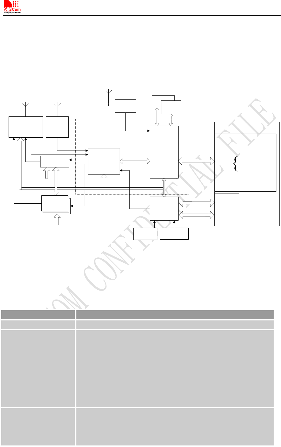
1.3 Hardware Diagram
The global architecture of the SIM5360A Embedded module is described in the figure below.
GSM/WCDMA
RF Frontend
GSM PA Transceiver
Processor
XO
19.2MHz
XO
32.768kHz
NAND
Flash
WCDMA
PA
MMC/SD
I2C
PCM
Interrupt
Status LED
USB
RTC
SIM
Power On
Reset
UART
GPIOs
ADC
LDO
Vbat*
Vbat*
Vbat* SPI
Keypad(Multiplex with GPIOs)
Sink Current Source
DDR
GNSS
RF
Main Antenna
GNSS Antenna
Power
Management
Qualcomm
Chip
SMT Interface
WCDMA
RF
Frontend
DIV Antenna
Figure 1: SIM5360A functional architecture
1.4 Functional Overview
Table 1: General Feature
Feature Implementation
Power supply Single supply voltage 3.4~4.2V
Transmission data
● Dual-mode UMTS/HSPA+/EDGE/GPRS operation
● GPRS Class B, multislot class 12 operation, Supports coding scheme:
CS1-4
● EDGE multislot class 12 operation, Supports coding schemes
MSC1-9
● UMTS R99 data rates-384 kbps DL/UL
● Category 6 HSDPA -14.4 Mbps HSUPA-5.76 Mbps
● CSD feature: 9.6, 14.4, 64 kbps UL/DL
GNSS
● GNSS engine (GPS and GLONASS)
● Protocol: NMEA
● Mobile-assisted mode
● Mobile-based mode
● Standalone mode

Smart Machine Smart Decision
SIM5360A_User_Manual_V1.03 2014-07-03
13
SMS
● MT, MO, CB, Text and PDU mode
● SMS storage: SIM card or ME(default)
● Support transmission of SMS alternatively over CSD or GPRS.
User can choose preferred mode.
SIM interface Support identity card: 1.8V, 3V.
Audio features(optional)
Speech codec modes:
● Half Rate (ETS 06.20)
● Full Rate (ETS 06.10)
● Enhanced Full Rate (ETS 06.50 / 06.60 / 06.80)
● AMR (WCDMA)
● AMR+QCP (GSM)
● A5/1, A5/2, and A5/3 ciphering
UART interface
● Support full mode or null mode
● Support AT command
USB Support USB2.0 Slave mode
Rx-diversity Support UMTS Rx-diversity.
Phonebook management Support phonebook types: SM, FD, LD, RC, ON, MC.
SIM application toolkit Support SAT class 3, GSM 11.14 Release 98
Support USAT
Real Time Clock Support RTC
Physical characteristics Size:30*30*2.9mm
Weight:5.7 g
Firmware upgrade Firmware upgrade over USB interface
PCM
Multiplex on GPIOs.
Used for analog audio function with external codec.
Support long frame sync and short frame sync.
Support 8-bit A-law, μ-law and 16-bit linear data formats.
Support master and slave mode, but must be the master in long frame
sync.
Temperature range
● Normal operation temperature: -10°C to +60°C
● Storage temperature -45°C to +90°C
2 Package Information
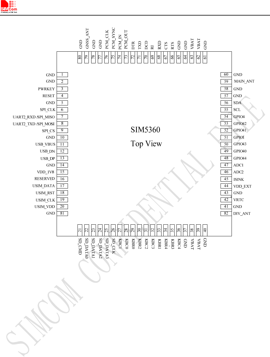
2.1 Pin Configuration
All hardware interfaces which connect SIM5360A to customers’ application platform are through 82 pins
pads (Metal half hole). Figure 2 is SIM5360A outline diagram.
Smart Machine Smart Decision
SIM5360A_User_Manual_V1.03 2014-07-03
14
Figure 2: Pin view

Smart Machine Smart Decision
SIM5360A_User_Manual_V1.03 2014-07-03
15
Table 2: Pin definition
Pin No. Define Pin No. Define
1 GND 2 GND
3 POWERKEY 4 RESET
5 GND 6 SPI_CLK
7 UART2_RXD / SPI_MISO 8 UART2_TXD / SPI_MOSI
9 SPI_CS 10 GND
11 USB_VBUS 12 USB_DN
13 USB_DP 14 GND
15 VDD_1V8 16 RESERVED
17 USIM_DATA 18 USIM_RST
19 USIM_CLK 20 USIM_VDD
21 SD_CMD 22 SD_DATA0
23 SD_DATA1 24 SD_DATA2
25 SD_DATA3 26 SD_CLK
27 KBC1 28 KBC0
29 KBR0 30 KBR2
31 KBC2 32 KBC3
33 KBR1 34 KBR4
35 KBR3 36 KBC4
37 GND 38 VBAT
39 VBAT 40 GND
41 GND 42 VRTC
43 GND 44 VDD_EXT
45 ISINK 46 ADC2
47 ADC1 48 GPIO44
49 GPIO40 50 GPIO43
51 NETLIGHT/GPIO1 52 GPIO41
53 GPIO42 54 GPIO4
55 SCL 56 SDA
57 GND 58 GND
59 MAIN_ANT 60 GND
61 GND 62 VBAT
63 VBAT 64 GND
65 GND 66 RTS

Smart Machine Smart Decision
SIM5360A_User_Manual_V1.03 2014-07-03
16
67 CTS 68 RXD
69 RI 70 DCD
71 TXD 72 DTR
73 PCM_OUT 74 PCM_IN
75 PCM_SYNC 76 PCM_CLK
77 GND 78 GND
79 GNSS_ANT 80 GND
81 GND 82 DIV_ANT
2.2 Pin description
IO Parameters Definition
Pin Type Description
PI Power input
PO Power output
IO Bidirectional input / output
DI Digital input
DO Digital output
AI Analog input
Table 3: Pin description
Pin name Pin No. I/O Description Comment
Power Supply
VBAT 38,39,
62,63 PI Power supply voltage
VRTC 42 I/O Power supply for RTC
If it is unused, keep open.
VDD_EXT 44 PO
LDO power output for SD card
circuit or other external circuit.
This LDO output voltage can be
changed by the AT command
“AT+CVAUXV”.
VDD_1V8 15 PO
The 1.8V SMPS output for
external circuit, such as level shift
circuit.
GND
1,2,5,10
,14,37,4
0,41,43,
57,58,6
0,61,64,
65,77,7
8,80,81
Ground
Power on/off

Smart Machine Smart Decision
SIM5360A_User_Manual_V1.03 2014-07-03
17
POWERKEY 3 DI
POWERKEY should be pulled
low at least 180ms to power on or
500ms to power off the module.
SD interface
SD_CMD 21 I/O SDIO command
If it is unused, keep open.
SD_DATA0 22 I/O SDIO data
SD_DATA1 23 I/O SDIO data
SD_DATA2 24 I/O SDIO data
SD_DATA3 25 I/O SDIO data
SD_CLK 26 DO SDIO clock
USIM interface
USIM_DATA 17 I/O SIM Data Output/Input
All signals of SIM
interface should be
protected against
ESD/EMC.
USIM_RST 18 DO SIM Reset
USIM_CLK 19 DO SIM Clock
USIM_VDD 20 PO Voltage Supply for SIM card
Support 1.8V or 3V SIM card
SPI/UART2 interface
SPI_CLK 6 DO SPI clock
If it is unused, keep open.
UART2_RXD
/SPI_MISO 7 DI
Receive data of UART2 / SPI
(master only) master in/slave out
data
UART2_TXD /
SPI_MOSI 8 DO
Transmit data of UART2 / SPI
(master only) master out/slave in
data
SPI_CS 9 DO SPI chip-select
USB
USB_VBUS 11 PI USB power supply input
They are compliant with
the USB 2.0 specification.
If it is unused, keep open.
USB_DN 12 I/O
Minus (-) line of the differential,
bi-directional USB signal to/from
the
USB_DP 13 I/O
Plus (+) line of the differential,
bi-directional USB signal to/from
the
UART1 interface
RTS 66 DO Request to send
RXD has been pulled
down with a 12kR resistor
to ground in the module.
If it is unused, keep open.
CTS 67 DI Clear to Send
RXD 68 DI Receive Data
RI 69 DO Ring Indicator
DCD 70 DO Carrier detects
TXD 71 DO Transmit Data
DTR 72 DI DTE get ready

Smart Machine Smart Decision
SIM5360A_User_Manual_V1.03 2014-07-03
18
I2C interface
SCL 55 DO I2C clock output None pulled up resistors in
the module. Pulled up with
a 2.2kR resistor to 1.8V
externally.
.
If it is unused, keep open.
SDA 56 I/O I2C data
Keypad interface
KBR0 29 DO Bit 0 drive to the pad matrix
All Keypad pins can be
configured as GPIOs.
If it is unused, keep open.
KBR1 33 DO Bit 1 drive to the pad matrix
KBR2 30 DO Bit 2 drive to the pad matrix
KBR3 35 DO Bit 3 drive to the pad matrix
KBR4 34 DO Bit 4 drive to the pad matrix
KBC0 28 DI Bit 0 for sensing key press on pad
matrix
KBC1 27 DI Bit 1 for sensing key press on pad
matrix
KBC2 31 DI Bit 2 for sensing key press on pad
matrix
KBC3 32 DI Bit 3 for sensing key press on pad
matrix
KBC4 36 DI Bit 4 for sensing key press on pad
matrix
PCM interface
PCM_OUT/GPIO5 73 DO PCM data output. It also can be
multiplexed as GPIO5.
If it is unused, keep open.
PCM_IN/GPIO0 74 DI
PCM data input. It also can be
multiplexed as GPIO0 with
module wake/interrupt.
PCM_SYNC/GPIO
2 75 DO
PCM data frame sync signal. It
also can be multiplexed as
GPIO2.
PCM_CLK/GPIO3 76 DO PCM data bit clock. It also can be
multiplexed as GPIO3.
GPIOs
NETLIGHT/GPIO1 51 DO Output PIN as LED control for
network status.
If it is unused, keep open.
GPIO4 54 DI Input PIN as RF operating
control.
GPIO40 49 DO Output PIN as operating status
indicating of module.
GPIO41 52 DO
General input/output PIN. It can
be used as wake/interrupt signal
to host from module
GPIO43 50 DI
General input/output PIN. It can
be used as wake/interrupt signal
to module from host.
Smart Machine Smart Decision
SIM5360A_User_Manual_V1.03 2014-07-03
19
GPIO44 48 I/O General input/output PIN.
GPIO42 53 I/O General input/output PIN.
RF interface
MAIN _ANT 59 MAIN ANT soldering pad
GNSS_ANT 79 AI GNSS ANT soldering pad
DIV_ANT 82 AI Diversity ANT soldering pad
Other interface
RESET 4 DI System reset in, active low.
ISINK 45 DI Current source of
ground-referenced current sink Refer to 3.13.1
ADC1 47 AI Analog Digital Converter Input Refer to 3.13.3
ADC2 46 AI Analog Digital Converter Input
RESERVED 16 Reserved
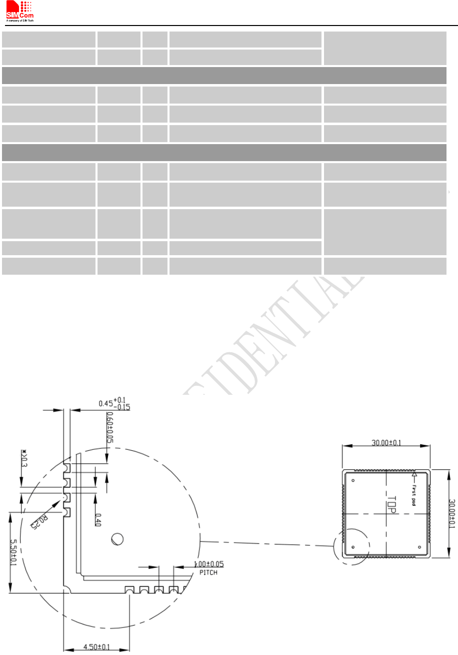
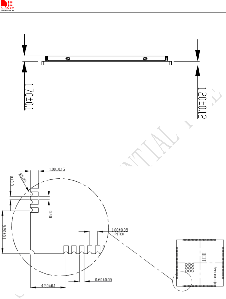
2.3 Package Dimensions
The following figure shows mechanical dimensions of SIM5360.
Figure 3: Top dimensions (Unit: mm)
Smart Machine Smart Decision
SIM5360A_User_Manual_V1.03 2014-07-03
20
Figure 4: Side dimensions (Unit: mm)
Figure 5: Bottom dimensions (Unit: mm)
Smart Machine Smart Decision
SIM5360A_User_Manual_V1.03 2014-07-03
21
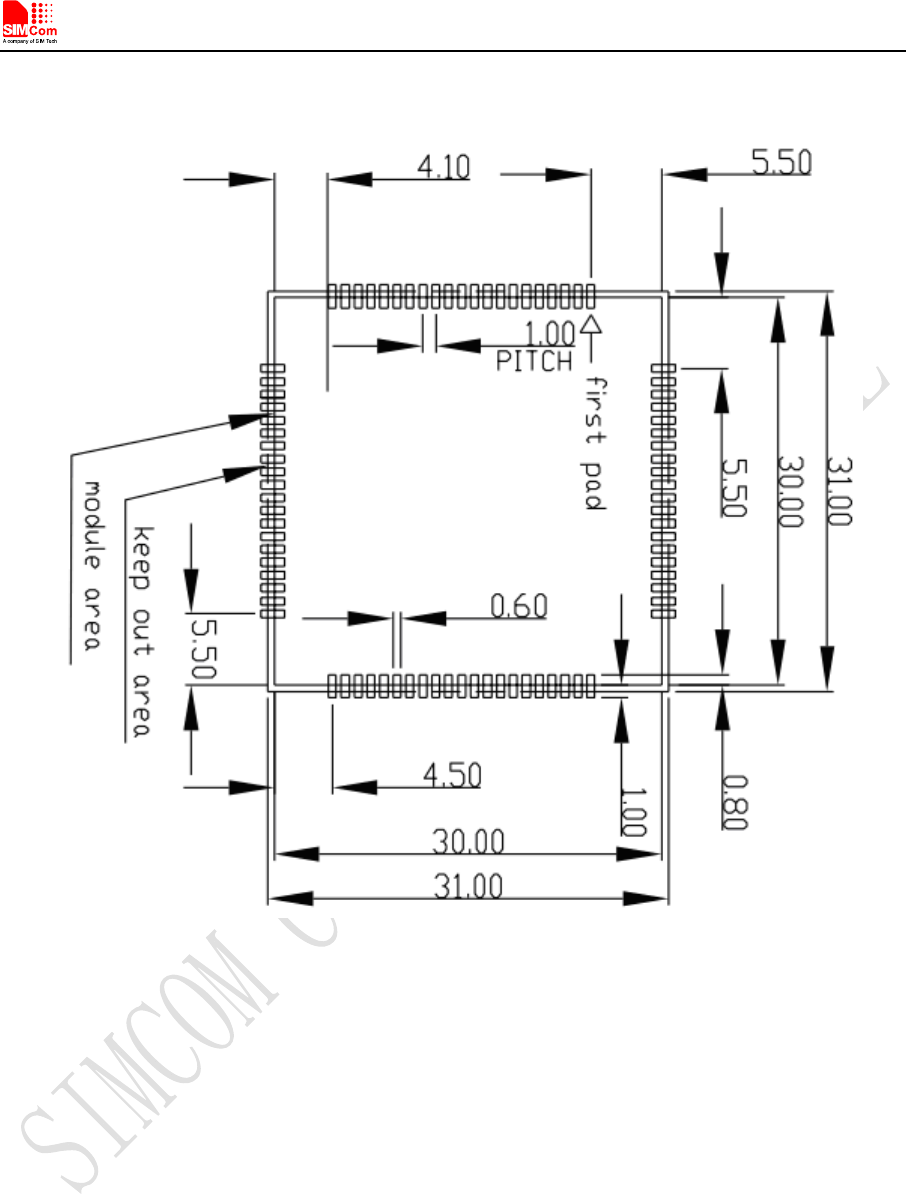
2.4 Footprint Recommendation
Figure 6: Footprint recommendation (Unit: mm)
3 Application Interface Specification
3.1 Power Supply
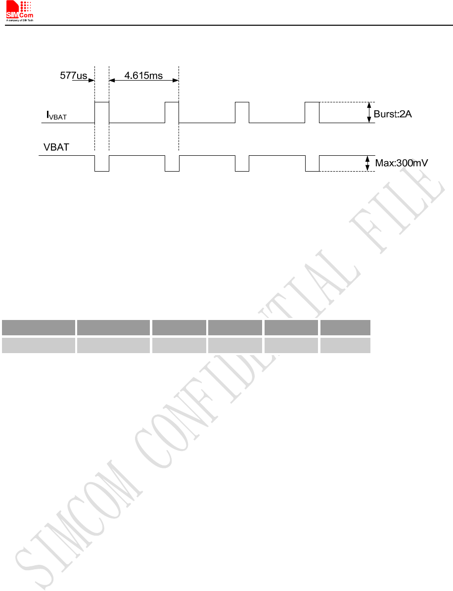
The power supply pins of SIM5360A include four VBAT pins (pin 62&63, pin 38&39). VBAT directly
supplies the power to RF circuit and baseband circuit. All four VBAT pins of SIM5360A must be used
together. VBAT directly supplies the power to RF PA and baseband system. For the VBAT, the ripple due
to GSM/GPRS emission burst (every 4.615ms)may cause voltage drop, and the current consumption rises
typically to peak of 2A. So the power supply must be able to provide sufficient current up to more than 2A.
The following figure is the VBAT voltage ripple wave at the maximum power transmit phase.
The test condition: VBAT =4.0V, VBAT maximum output current =2A, CA=100 µF tantalum capacitor
Smart Machine Smart Decision
SIM5360A_User_Manual_V1.03 2014-07-03
22
(ESR=0.7Ω) and CB=1µF(Please refer to Figure 8—Application circuit).
Figure 7: VBAT voltage drop during burst emission (GSM/GPRS)
3.1.1 Power Supply Pin
Two VBAT pins are dedicated to connect the supply voltage.
Table 4: Pin description
Pin type Pin name Min Typ Max Unit
POWER VBAT 3.4 3.8 4.2 V
Note:
1. When the module is power off, users must pay attention to the issue about current leakage. Refer to
Chapter 3.10.2.
3.1.2 Design Guide
Make sure that the input voltage at the VBAT pin will never drop below 3.3V even during a transmit burst
when the current consumption rises up to more than 2A. If the power voltage drops below 3.3V, the
module may be shut down automatically. Using large tantalum capacitors (above 100uF) will be the best
way to reduce the voltage drops. If the power current cannot support up to 2A, users must introduce larger
capacitor (typical 1000uF) to storage electric power, especially GPRS multiple time slots emission.
For the consideration of RF performance and system stability, some multi-layer ceramic chip (MLCC)
capacitors (0.1/1uF) need to be used for EMC because of their low ESR in high frequencies. Note that
capacitors should be put beside VBAT pins as close as possible. Also User should minimize the PCB trace
impedance from the power supply to the VBAT pins through widening the trace to 80 mil or more on the
board. The following figure is the recommended circuit.
In addition, in order to get a stable power source, it is suggested to use a zener diode of which reverse
zener voltage is 5.1V and dissipation power is more than 500mW.
Smart Machine Smart Decision
SIM5360A_User_Manual_V1.03 2014-07-03
23
Table 5: Recommended zener diode models
No. Manufacturer Part Number Power Package
1 On semi MMSZ5231BT1G 500mW SOD123
2 Prisemi PZ3D4V2H 500mW SOD323
3 Prisemi PZ5D4V2H 500mW SOD523
4 Vishay MMSZ4689-V 500mW SOD123
5 Crownpo CDZ55C5V1SM 500mW 0805
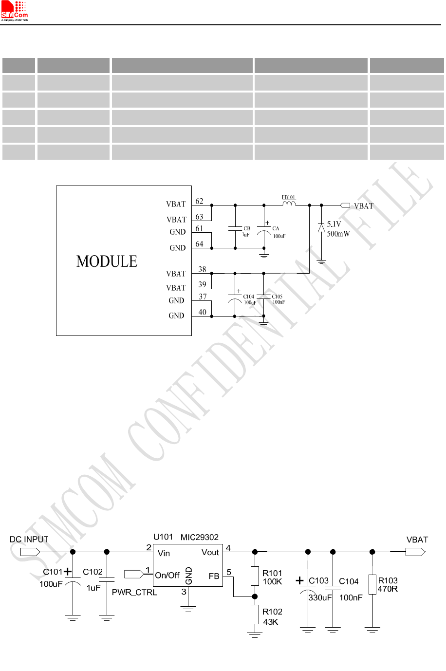
Figure 8: VBAT input application circuit
There are three sections about how to design and optimize users’ power systems.
Power supply circuit
We recommend DCDC or LDO is used for the power supply of the module, make sure that the peak
current of power components can rise up to more than 2A. The following figure is the reference design of
+5V input power supply. The designed output for the power supply is 4.1V, here a linear regulator can be
used.
Figure 9: Reference circuit of the LDO power supply
If there is a big difference between the input voltage and the desired output (VBAT), a switching converter
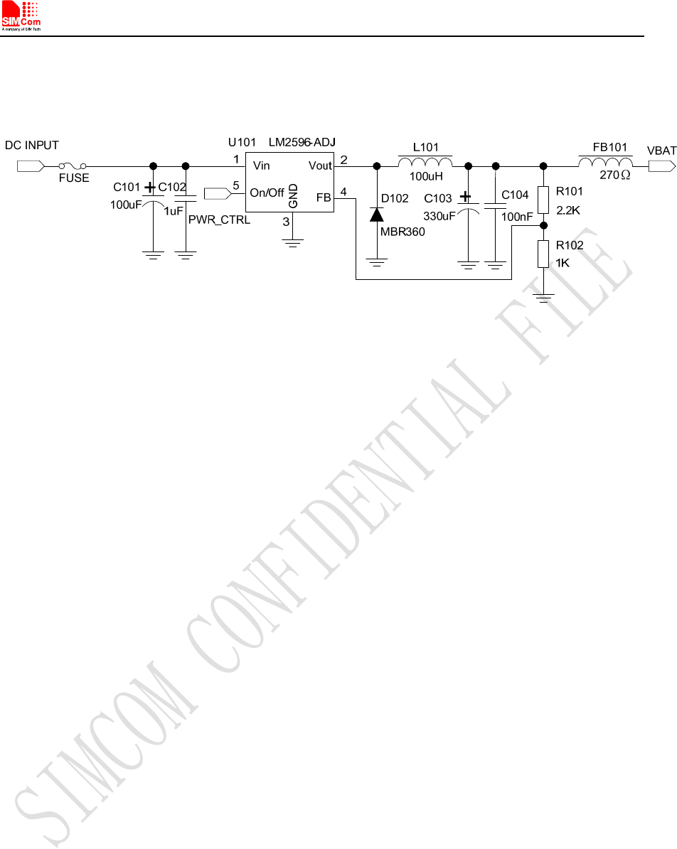
Smart Machine Smart Decision
SIM5360A_User_Manual_V1.03 2014-07-03
24
power will be preferable because of its better efficiency, especially at the high current situation. The
following figure is the reference circuit. Note that DCDC may deprave RF performance because of ripple
current intrinsically.
Figure 10: Reference circuit of the DCDC power supply
Volta ge monito r
To monitor the power supply voltage, user can use the AT command “AT+CBC”, this command has two
parameters: the battery status and the voltage value (mV). It will return the capacity percentage and actual
value of battery (at the VBAT pin). The voltage is continuously measured at intervals, whenever the
measured battery voltage is lower than a specific value set by the AT command “AT+CVALARM”. For
example, if the voltage value is set to be 3.4V, the following URC will be presented: “warning! voltage is
low: 3.3v”.
If the voltage is lower than a specific value which is set by the AT command “AT+CPMVT”, the module
will be powered off automatically and AT commands cannot be executed any more.
Note: Under-voltage warning function is disabled by default, user can enable it by the AT command
“AT+CVALARM”. Please refer to Document [1].
3.1.3 RTC Backup
The module uses RTC (Real Time Clock) to update and maintain inherent time and keeps system alive at
no power supply status. The RTC power supply of module can be provided by an external capacitor or a
battery (non-chargeable or rechargeable) through the VRTC. The following figures show various reference
circuits for RTC back up. The discharge current is less than 10uA.
External capacitor backup
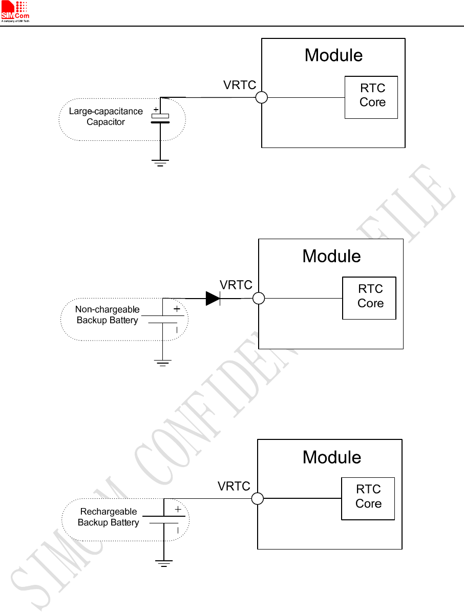
Smart Machine Smart Decision
SIM5360A_User_Manual_V1.03 2014-07-03
25
Figure 11: RTC supply from capacitor
Non-chargeable battery backup
Figure 12: RTC supply from non-chargeable battery
Rechargeable battery backup
Figure 13: RTC supply from rechargeable battery
Coin-type rechargeable battery is recommended, such as ML414H-IV01E form Seiko can be used.
Note: The VRTC can be disabled, jus disconnect it in application circuit.
Smart Machine Smart Decision
SIM5360A_User_Manual_V1.03 2014-07-03
26
3.2 Power on/off Time Sequence
3.2.1 Power on Sequence
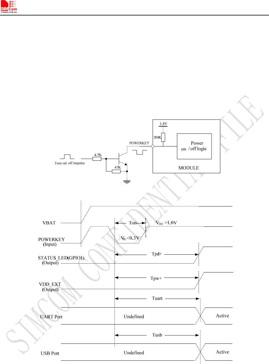
SIM5360A can be powered on by POWERKEY pin, which starts normal operating mode.
POWERKEY pin is pulled up with a 200k ohm resistor to 1.8V in module. User can power on the
SIM5360A by pulling the POWERKEY pin down for a short time. The power-on scenarios are illustrated
in the following figures.
Figure 14: Power on Timing Sequence

Smart Machine Smart Decision
SIM5360A_User_Manual_V1.03 2014-07-03
27
Table 6: Power on timing
Symbol Parameter Time value Unit
Min. Typ. Max.
Ton The time to pull POWERKEY down to power on 180 500 - ms
TpD+ The time to indicate connecting with the network - - 5 s
Tpw+ The time to indicate the module is powered on
completely - - 0.5 s
Tuart The time to enable UART - - 8 s
Tusb The time to enable USB - - 10 s
Note: Module could be automatically power on by connecting Power ON pin to Low level directly.
Before designing, please refer to Document [27] for more detail.
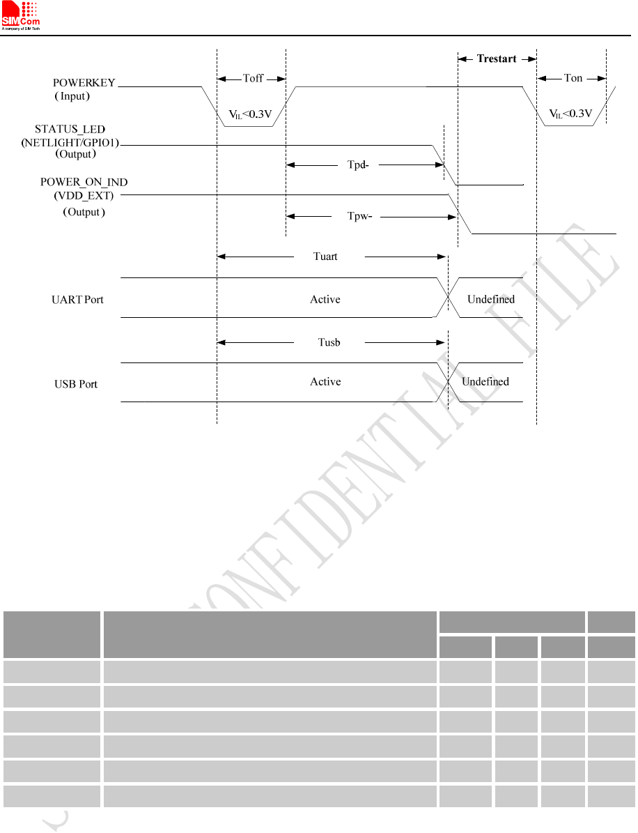
3.2.2 Power off Sequence
The following methods can be used to power down SIM5360. These procedures will make module
disconnect from the network and allow the software to enter a safe state, and then save data before
completely powering the module off.
● Method 1: Power off SIM5360A by pulling the POWERKEY pin down
● Method 2: Power off SIM5360A by AT command
User can power off the SIM5360A by pulling POWERKEY down for a specific time. The power off
scenario is illustrated in the following figure.
Smart Machine Smart Decision
SIM5360A_User_Manual_V1.03 2014-07-03
28
Figure 15: Power off timing sequence
Table 7: Power off timing
Symbol Parameter Time value
Min. Typ. Max. Unit
Toff The time pulling POWERKEY down to power off 0.5 - 5 s
TpD- The time to indicate disconnecting from the network - - 2 s
Tpw- The time to indicate the module power off completely - - 2 s
Tuart The time to disable UART - - 3 s
Tusb The time to disable USB - - 2 s
Trestart The time to power on again after Tpw- 0 - - s
User can also use the AT command “AT+CP OF ” to power down the module. After that, the AT commands
cannot be executed any longer. The module enters the POWER DOWN mode, only the RTC is still active.
For details, refer to Document [1].
3.3 UART Interface
SIM5360A provides two UARTs (universal asynchronous serial transmission) port. UART1 consists of a
flexible 7-wire serial interface. UART2 consists of 2-wire serial interface. The module is as the DCE (Data
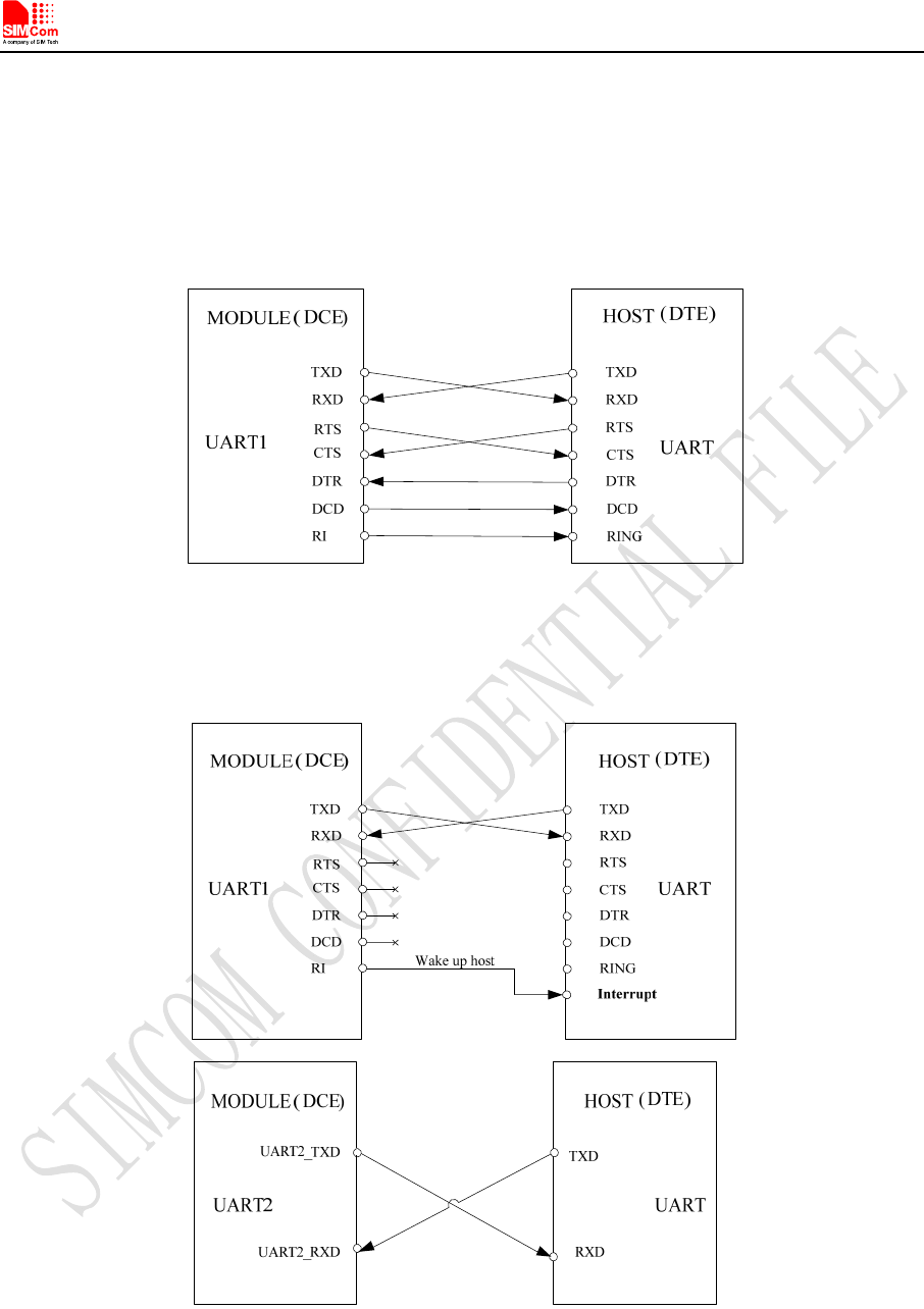
Smart Machine Smart Decision
SIM5360A_User_Manual_V1.03 2014-07-03
29
Communication Equipment) and the client PC is as the DTE (Data Terminal Equipment). AT commands
are entered and serial communication is performed through UART interface.
In order to prevent the UART signals of the module damaged due to voltage spikes or ESD, series resistors
can be used on UART signals.
The application circuit is in the following figures.
Figure 16: UART1 Full modem
Figure 17: Null modem (UART1 and UART2)
Smart Machine Smart Decision
SIM5360A_User_Manual_V1.03 2014-07-03
30
3.3.1 Pin Description
Table 8: Pin description
Pin type Pin name Pin No. I/O Default Status
UART1
RXD 68 I Pull-Down
TXD 71 O Pull-Up
RTS 66 O
CTS 67 I Pull-Up
DTR 72 I Pull-Up
DCD 70 O
RI 69 O
UART2
UART2_RXD 7 I Pull-Down
UART2_TXD 8 O Pull-Up
More pin information refers to chapter 2.2.
Table 9: Logic level
Symbol Parameter Min Typ Max Unit
VIH High-level input voltage 1.26 1.8 2.1 V
VIL Low-level input voltage -0.3 0 0.63 V
VOH High-level output voltage 1.35 1.8 1.8 V
VOL Low-level output voltage 0 0 0.45 V
3.3.2 Application Guide
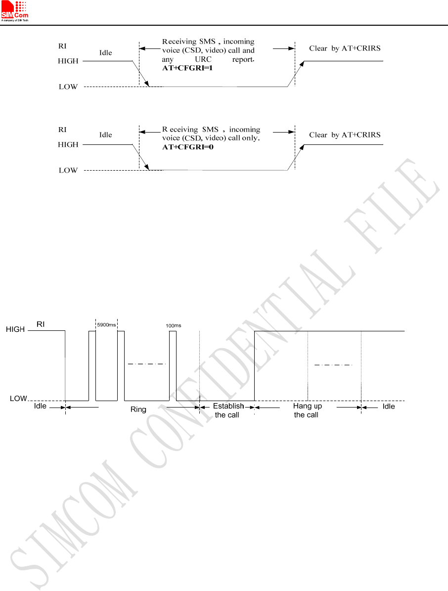
If UART port is used in Null Modem, the pin “RI” can be used as an interrupt signal to HOST. Normally it
will keep high logic level until certain condition such as receiving SMS, voice call (CSD, video) or URC
reporting, then “RI” will change to low logic level to inform the master (client PC). It will stay low until
the master clears the interrupt event with AT command.
Smart Machine Smart Decision
SIM5360A_User_Manual_V1.03 2014-07-03
31
Figure 18: RI behaviour in NULL Modem
If Full Modem is used to establish communication between devices, the pin “RI” is another operation
status. Initially it keeps high, when a voice call or CSD call comes, the pin “RI” will change to low for
about 5900ms, then it will return to high level for 100ms. It will repeat this procedure until this call is
answered or hung up.
Figure 19: RI behaviour in FULL Modem
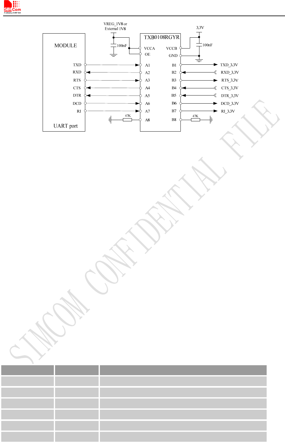
The SIM5360A UART is 1.8V interface. A level shifter should be used if user’s application is equipped
with a 3.3V UART interface. The level shifter TXB0108RGYR provided by Texas Instruments is
recommended. The reference design of the TXB0108RGYR is in the following figures.
Smart Machine Smart Decision
SIM5360A_User_Manual_V1.03 2014-07-03
32
Figure 20: Reference circuit of level shift
To comply with RS-232-C protocol, the RS-232-C level shifter chip should be used to connect SIM5360A
to the RS-232-C interface. In this connection, the TTL level and RS-232-C level are converted mutually.
SIMCom recommends that user uses the SP3238ECA chip with a full modem. For more information
please refers to the RS-232-C chip datasheet.
Note: SIM5360A supports the baud rate: 300, 600, 1200, 2400, 4800, 9600, 19200, 38400, 57600,
115200, 230400, 460800, 921600, 3200000, 3686400, 4000000bps. Default rate is 115200bps.
3.4 SD/MMC Interface
SIM5360A provides one 4-bit SD/MMC interface. Its operation voltage is 2.85V, with clock rates up to 52
MHz. It supports 1-bit SD/MMC or 4-bit SD data transmission mode. Though the same hardware
controller is used, the initialization procession for SD or MMC cards is different. SIM5360A will detect
which card is inserted automatically.
Note: Interface with SD/MMC memory cards up to 32GB.
3.4.1 Pin Description
Table 10: Pin description
Pin name Pin No. Function
SD_DATA0 22 SD/MMC card data0
SD_DATA1 23 SD card data1
SD_DATA2 24 SD card data2
SD_DATA3 25 SD card data3
SD_CLK 26 SD card clock
SD_CMD 21 SD card command
Smart Machine Smart Decision
SIM5360A_User_Manual_V1.03 2014-07-03
33
Table 11: Electronic characteristic
Symbol Parameter Min Typ Max Unit
VDD_EXT LDO power output 2.71 2.85 2.99 V
VIH High-level input voltage 0.65·VDD_EXT - VDD_EXT+0.3 V
VIL Low-level input voltage -0.3 0 0.3·VDD_EXT V
VOH High-level output voltage 2.71 2.85 2.99 V
VOL Low-level output voltage 0 0 0.45 V
3.4.2 Design guide
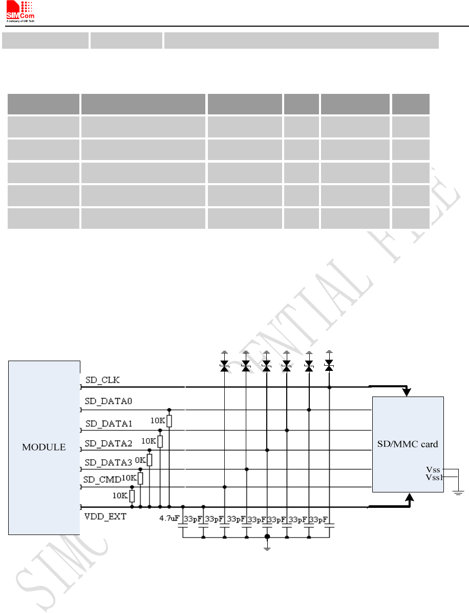
The module provides a LDO named VDD_EXT for SD card power supply. The LDO is 2.85V by default,
capable of 300mA. Data lines should be pulled up to VDD_EXT by 10K resistors. ESD/EMI components
should be arranged beside SD card socket. Refer to the following application circuit.
Figure 21: SD interface circuit
3.5 USIM Interface
The USIM provides the required subscription verification information to allow the mobile equipment to
attach to a GSM or UMTS network. Both 1.8V and 3.0V SIM Cards are supported.
3.5.1 Pin description
Table 12: Pin description
VDD_EXT 44 SD card power
Smart Machine Smart Decision
SIM5360A_User_Manual_V1.03 2014-07-03
34
Table 13: Electronic characteristic
Symbol Parameter
3.0V mode 1.8V mode
Unit
Min Typ Max Min Ty
p Max
USIM_VD
D
LDO power
output
2.71 2.85 3.05 1.7 1.8 1.9
V
VIH High-level
input voltage
0.65·USI
M_VDD - USIM_V
DD +0.3
0.65·USI
M_VDD - USIM_V
DD +0.3 V
VIL Low-level
input voltage -0.3 0 0.3·USI
M_VDD -0.3 0 0.3·USI
M_VDD V
VOH High-level
output voltage
2.71 2.85 3.05 1.7 1.8 1.9 V
VOL Low-level
output voltage 0 0 0.45 0 0 0.45 V
3.5.2 Application Guide
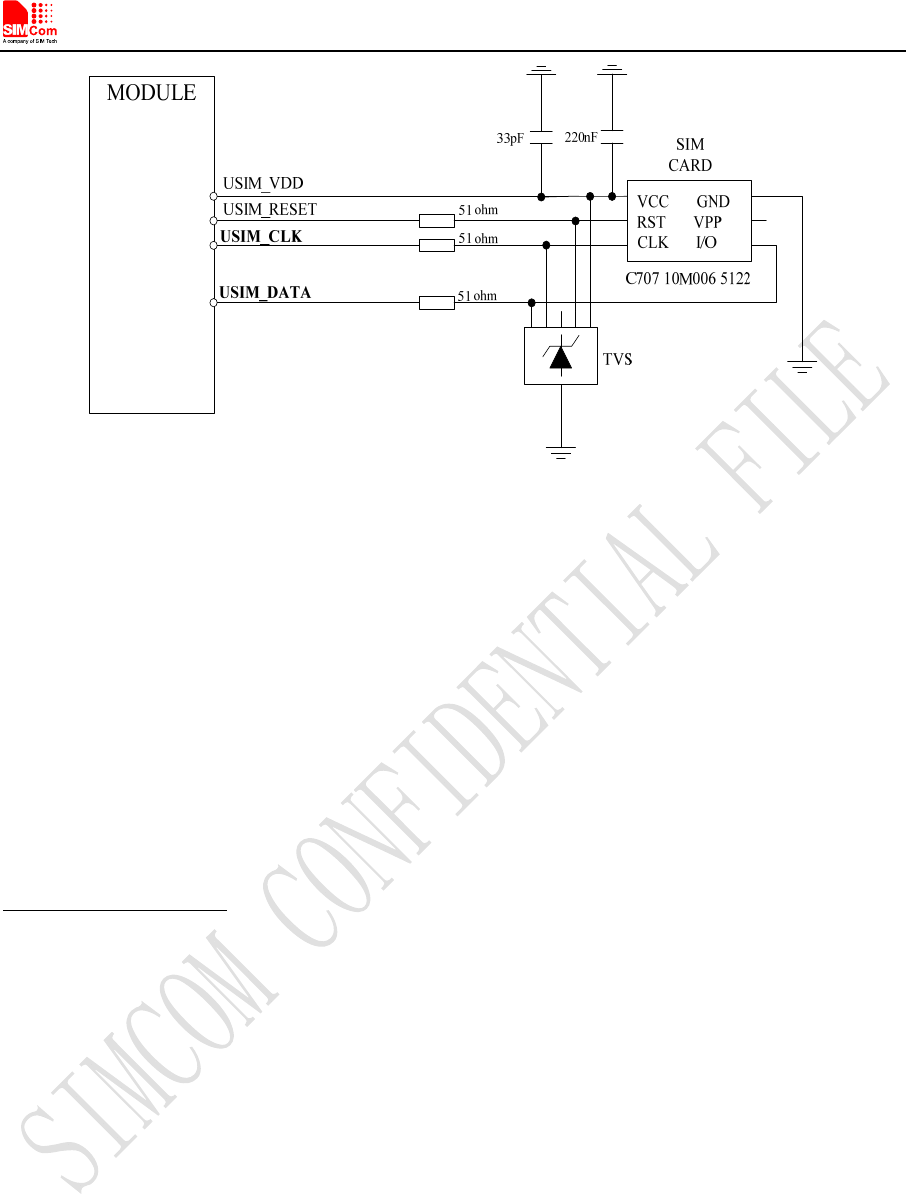
It is recommended to use an ESD protection component such as ST (www.st.com ) ESDA6V1W5 or ON
SEMI (www.onsemi.com ) SMF05C. Note that the SIM peripheral circuit should be close to the SIM card
socket. The reference circuit of the 6-pin SIM card holder is illustrated in the following figure.
Pin name Pin Description
USIM_CLK 19 USIM Card Clock
USIM_RST 18 USIM Card Reset
USIM_DATA 17
USIM Card data I/O, which has been pulled up with a 22kR resistor to
USIM_VDD in module. Do not pull up or pull down in users’
application circuit.
USIM_VDD 20 USIM Card Power output depends automatically on USIM mode,one
is 3.0V±10%, another is 1.8V±10%. Current is less than 50mA.
Smart Machine Smart Decision
SIM5360A_User_Manual_V1.03 2014-07-03
35
Figure 22: USIM interface reference circuit
Note: USIM_DATA has been pulled up with a 15kohm resistor to USIM_VDD in module. A 220nF shut
capacitor on USIM_VDD is used to reduce interference. Use AT Commands to get information in USIM
card. For more detail, please refer to document [1].
3.5.3 Recommend Components
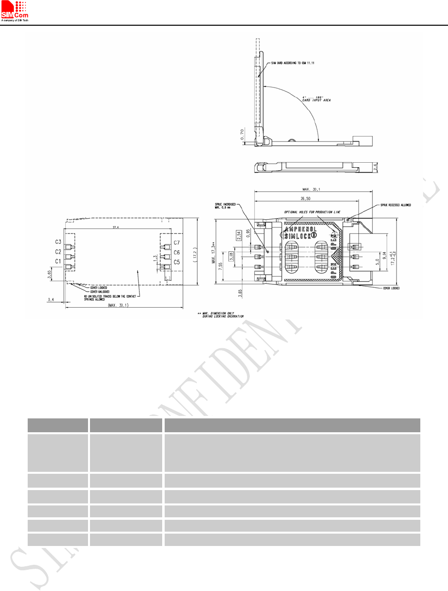
For 6 pins USIM socket, SIMCom recommend to use Amphenol C707 10M006 512 2. User can visit
http://www.amphenol.com for more information about the holder.
Smart Machine Smart Decision
SIM5360A_User_Manual_V1.03 2014-07-03
36
Figure 23: Amphenol SIM card socket
Table 19: Amphenol USIM socket pin description
Pin Signal Description
C1 USIM_VDD
SIM Card Power supply, it can identify automatically the
SIM Card power mode,one is 3.0V±10%, another is
1.8V±10%.
C2 USIM_RST SIM Card Reset.
C3 USIM_CLK SIM Card Clock.
C5 GND Connect to GND.
C6 VPP
C7 USIM_DATA SIM Card data I/O.
3.6 I2C Interface
I2C is used to communicate with peripheral equipments and can be operated as either a transmitter or
receiver, depending on the device function. Use AT Commands “AT+CRIIC and AT+CWIIC” to read/write
register values of related peripheral equipments connected with I2C interface. Its operation voltage is
1.8V.

Smart Machine Smart Decision
SIM5360A_User_Manual_V1.03 2014-07-03
37
3.6.1 Pin Description
Table 14: Pin description
3.6.2 Signal Description
Both SDA and SCL are bidirectional lines, connected to a positive supply via a pull-up resistor
respectively. When the bus is free, both lines are high.
3.6.3 Design Guide
For SIM5360, the data on the I2C bus can be transferred at rates up to 400kbps. The number of peripheral
devices connected to the bus is solely dependent on the bus capacitance limit of 400pF. Note that PCB
traces length and bending are in users’ control to minimize load capacitance.
Note
:
SDA and SCL have none pulled up resistors in module. So there is need to pull them up in users’
application circuit.
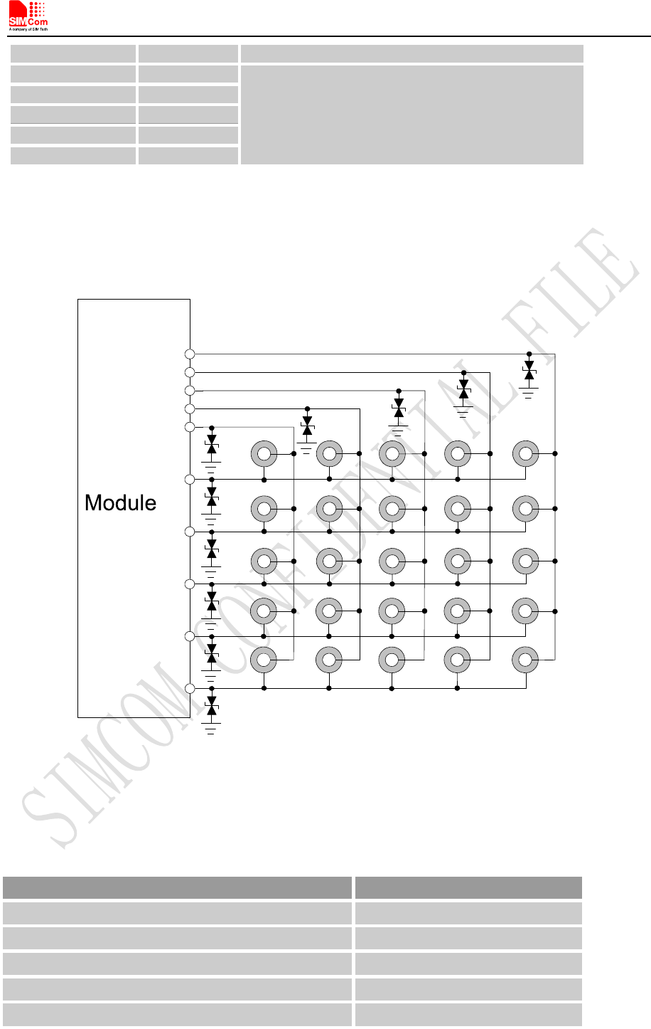
3.7 Keypad Interface
SIM5360A module provides a keypad interface that supports five sense lines, or columns, and five keypad
rows. The interface generates an interrupt when any key is pressed. Its operation voltage is 1.8V.
3.7.1 Pin Description
Table 15: Pin description
Pin name Pin No. Function
KBC0 28
Sensing keys
KBC1 27
KBC2 31
KBC3 32
Pin name Pin No. Function
SDA 56 Serial interface data input and output
SCL 55 Serial interface clock input
Smart Machine Smart Decision
SIM5360A_User_Manual_V1.03 2014-07-03
38
KBC4 36
KBR0 30
Driving pads
KBR1 29
KBR2 30
KBR3 35
KBR4 34
3.7.2 Application Guide
All keypad pins can be configured for GPIOs. These GPIOs also support interruption operation if used as
input pins. A typical circuit about the keypad (5*5 keypad matrix) is shown in the following figure.
KBR4
KBR3
KBR2
KBR1
KBR0
KBC0
KBC1
KBC2
KBC3
KBC4
Figure 24: Reference circuit
If these pins are configured for GPIOs, the sequence is listed in the following table.
Table 16: GPIO configuration
Keypad interface GPIO No.
KBR4 GPIO6
KBR3 GPIO7
KBR2 GPIO8
KBR1 GPIO9
KBR0 GPIO10
Smart Machine Smart Decision
SIM5360A_User_Manual_V1.03 2014-07-03
39
KBC4 GPIO11
KBC3 GPIO12
KBC2 GPIO13
KBC1 GPIO14
KBC0 GPIO15
Note: Refer to document [23] for detailed information of Keypad Application Note.
3.8 USB Interface
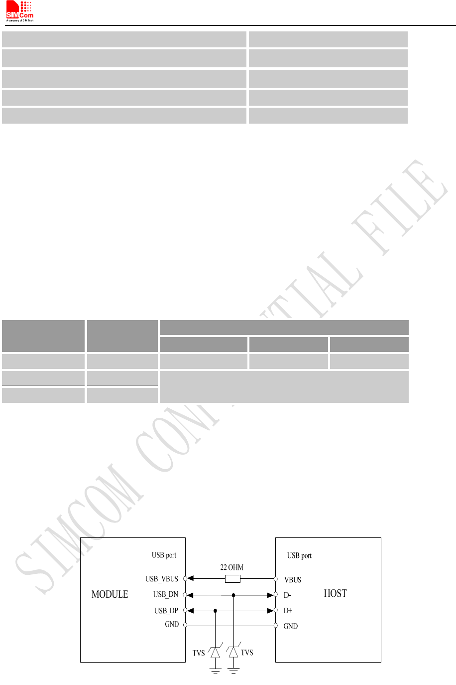
SIM5360A module contains a USB interface. This interface is compliant with the USB2.0 specification.
The USB2.0 specification requires hosts such as the computer to support all three USB speeds, namely
low-speed (1.5Mbps), full-speed (12Mbps) and high-speed (480Mbps). USB charging and USB-OTG is
not supported.
Table 17: Electronic characteristic
Pin name Pin No. Input voltage scope( V )
Min Typ Max
USB_VBUS 11 3 5.0 5.25
USB_DP 13 They are compliant with the USB 2.0 specification.
USB_DN 12
3.8.1 Application Guide
Currently SIM5360A supports the USB suspend and resume mechanism which can help to save power.
If no transaction is on USB bus, SIM5360A will enter suspend mode. When some events such as voice call
or receiving SMS happen, SIM5360A will resume normal mode automatically.
Figure 25: USB interface

Smart Machine Smart Decision
SIM5360A_User_Manual_V1.03 2014-07-03
40
Because of high bit rate on USB bus, pay attention to influence of junction capacitance of ESD component
on USB data lines. Typically, the capacitance should be less than 4pF @1MHz.
It is recommended to use an ESD protection component such as ON SEMI (www.onsemi.com )
ESD9M5.0ST5G or ESD9L5.0ST5G.
Note
:
The SIM5360A has two kinds of interface (UART and USB) to connect to host CPU. USB
interface is mapped to five virtual ports: “SIMTECH HS-USB Modem 9000”, “SIMTECH HS-USB
NMEA 9000”, “SIMTECH HS-USB AT port 9000”, “SIMTECH HS-USB Diagnostics 9000” and
“SIMTECH Wireless HS-USB Ethernet Adapter 9000”.
3.9 SPI Interface
SPI interface of SIM5360A is master only. It provides a duplex, synchronous, serial communication link
with peripheral devices. Its operation voltage is 1.8V, with clock rates up to 26 MHz.
3.9.1 Pin Description
Table 18: Pin description
Table 19: Electronic characteristic
Symbol Parameter Min Typ Max Unit
VIH High-level input voltage 1.26 1.8 2.1 V
VIL Low-level input voltage -0.3 0 0.63 V
VOH High-level output voltage 1.35 1.8 1.8 V
VOL Low-level output voltage 0 0 0.45 V
3.10 GPIO Interface
SIM5360A provides a limited number of GPIO pins. All GPIOs can be configured as inputs or outputs.
User can use AT Commands to read or write GPIOs status. Refer to ATC document for details.
Pin name Pin No. Function
SPI_CS 9 SPI chip-select; not mandatory in a point-to-point connection
SPI_MISO 7 SPI master in/slave out data
SPI_CLK 6 SPI clock
SPI_MOSI 8 SPI master out/slave in data

Smart Machine Smart Decision
SIM5360A_User_Manual_V1.03 2014-07-03
41
3.10.1 Pin Description
Table 20: Pin description
Note: If more GPIOs need to be used, users can configure GPIO on other multiple function interfaces,
such as PCM. Please refer to GPIO list.
Table 21: Electronic characteristic
Symbol Parameter Min Typ Max Unit
VIH High-level input voltage 1.26 1.8 2.1 V
VIL Low-level input voltage -0.3 0 0.63 V
VOH High-level output voltage 1.35 1.8 1.8 V
VOL Low-level output voltage 0 0 0.45 V
Note: The output driver current of GPIOs is 2mA.
Pin name Pin No. I/O Function
NETLIGHT/GPIO1 51 O Output PIN as LED control for network status. If it is
unused, left open.
GPIO4 54 I
Input PIN as RF operating control.
H: Normal Mode L:Flight Mode
If it is unused, left open.
GPIO40 49 O
Output PIN as operating status indicating of module.
H: Power on L: Power off
If it is unused, left open.
GPIO41 52 I/O General input/output PIN. It can be used as wake/interrupt
signal to host from module If it is unused, left open.
GPIO42 53 I/O General Purpose Input/Output Port.
GPIO43 50 I/O
General Purpose Input/Output Port. It can be used as
wake/interrupt signal to module from host. If it is unused, left
open.
GPIO44 48 I/O General Purpose Input/Output Port
Smart Machine Smart Decision
SIM5360A_User_Manual_V1.03 2014-07-03
42
3.10.2 Application Guide
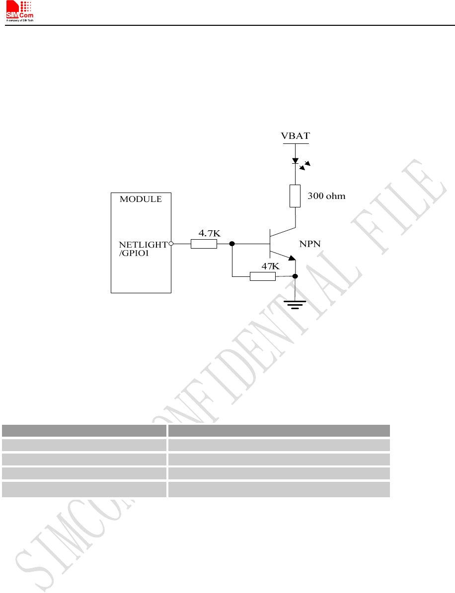
Network status
GPIO1 is used to control Network Status LED; application circuit is shown below.
Figure 26: Application circuit
Note: The value of resistor Rx depends on LED characteristic.
Table 22: LED status
LED Status Module Status
Always On Searching Network/Call Connect
200ms ON, 200ms OFF Data Transmit
800ms ON, 800ms OFF Registered network
Off Power off / Sleep
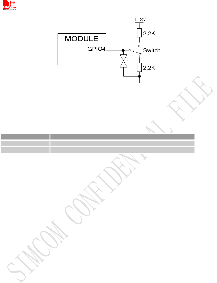
Flight mode control
GPIO4 controls SIM5360A module to enter or exit the Flight mode. In Flight mode, SIM5360A closes RF
function to prevent interference with other equipments or minimize current consumption. Bidirectional
ESD protection component is suggested to add on GPIO4.
Smart Machine Smart Decision
SIM5360A_User_Manual_V1.03 2014-07-03
43
Figure 27: Flight mode switch
Table 23: Control status
GPIO4 Status Module operation
Low Level Flight Mode: RF is closed.
High Level Normal Mode: RF is working.
Note
:
1. For SIM5360, GPIO0, GPIO2, GPIO3 and GPIO5 have multiplex function, user can use them
as PCM interface to connect extend codec. Refer to section 3.11 and document [1] for details.
2. When the module is powered off, make sure all digital interfaces (PCM UART, etc) connected with
peripheral devices have no voltage higher than 0.3V. If users’ design cannot meet above conditions,
high level voltages maybe occur in GPIO pins because current leakage from above digital interfaces
may occur.
3.11 PCM Interface
SIM5360A provides hardware PCM interface for external codec. The PCM interface enables
communication with an external codec to support hands-free applications. SIM5360A PCM interface can
be used in two modes: the default mode is auxiliary PCM (8 KHz long sync mode at 128 KHz PCM CLK);
the other mode is primary PCM (8 KHz short sync mode at 2048 KHz PCM CLK). In short-sync
(primary PCM) mode, SIM5360A can be a master or a slave. In long-sync (auxiliary PCM) mode,
SIM5360A is always a master. SIM5360A also supports 3 kinds of coding formats: 8 bits (-law or A-law)
and 16 bits (linear).
Note: PCM interface is multiplexed from GPIO (default setting). The AT command “AT+CPCM” is
used to switch between PCM and GPIO functions. Please refer to document [21] and document [1] for
details.
Smart Machine Smart Decision
SIM5360A_User_Manual_V1.03 2014-07-03
44
3.11.1 Pin Description
Table 24: Pin description
Pins Pin No. Description
PCM_OUT 73 PCM data output
PCM_IN 74 PCM data input
PCM_SYNC 75 PCM data synchrony
PCM_CLK 76 PCM data clock
Table 25: Electronic characteristic
Symbol Parameter Min Typ Max Unit
VIH High-level input voltage 1.26 1.8 2.1 V
VIL Low-level input voltage -0.3 0 0.63 V
VOH High-level output voltage 1.35 1.8 1.8 V
VOL Low-level output voltage 0 0 0.45 V
3.11.2 Signal Description
The default PCM interface in SIM5360A is the auxiliary PCM interface. The data changes on the high
level of PCM_CLK and is sampled at the falling edge of PCM_CLK in one period. Primary PCM is
disabled after every power-on or every reset event. So user must use AT command to enable the primary
PCM mode after powering on or resetting the module every time if user wants to use Primary
PCM.SIM5360A PCM Interface can be operated in Master or Slave mode if it is configured to primary
PCM. In Master Mode, the Module drives the clock and sync signals that are sent to the external codec.
When it is in Slave Mode, the external codec drives the clock and sync signals which are sent to the
module. Both PCM modes are discussed in this section followed by additional PCM topics.
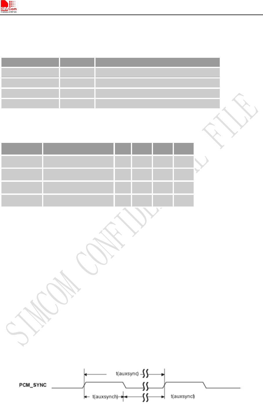
Auxiliary PCM (128 KHz PCM clock)
-law coding is supported by the auxiliary PCM. The auxiliary codec port operates with standard
long-sync timing and a 128 KHz clock. The AUX_PCM_SYNC runs at 8 KHz with 50% duty cycle.
Most -law codec support the 128 KHz clock.
Figure 28: Synchrony timing
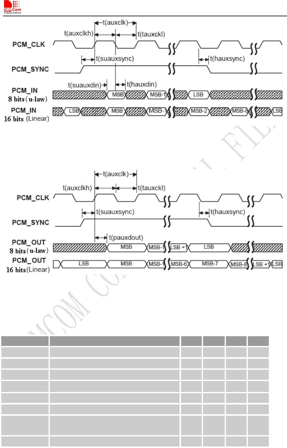
Smart Machine Smart Decision
SIM5360A_User_Manual_V1.03 2014-07-03
45
Figure 29: EXT CODEC to MODULE timing
Figure 30: MODULE to EXT CODEC timing
Table 26: Timing parameters
Parameter Description Min Typ Max Unit
T(auxsync) AUX_PCM_SYNC cycle time – 125 - μs
T(auxsynch) AUX_PCM_SYNC high time 62.4 62.5 - μs
T(auxsyncl) AUX_PCM_SYNC low time 62.4 62.5 - μs
T(auxclk)* AUX_PCM_CLK cycle time - 7.8 – μs
T(auxclkh) AUX_PCM_CLK high time 3.8 3.9 – μs
T(auxclkl) AUX_PCM_CLK low time 3.8 3.9 – μs
T(suauxsync) AUX_PCM_SYNC setup time high before
falling edge of PCM_CLK 1.95 – – μs
T(hauxsync) AUX_PCM SYNC hold time after falling edge 1.95 – – μs
Smart Machine Smart Decision
SIM5360A_User_Manual_V1.03 2014-07-03
46
of PCM_CLK
T(suauxdin) AUX_PCM_IN setup time before falling edge
of AUX_PCM_CLK 70 – – ns
T(hauxdin) AUX_PCM_IN hold time after falling edge of
AUX_PCM_CLK 20 – – ns
T(pauxdout) Delay from AUX_PCM_CLK rising to
AUX_PCM_OUT valid – – 50 ns
*Note: T(auxclk) = 1/(128 KHz).
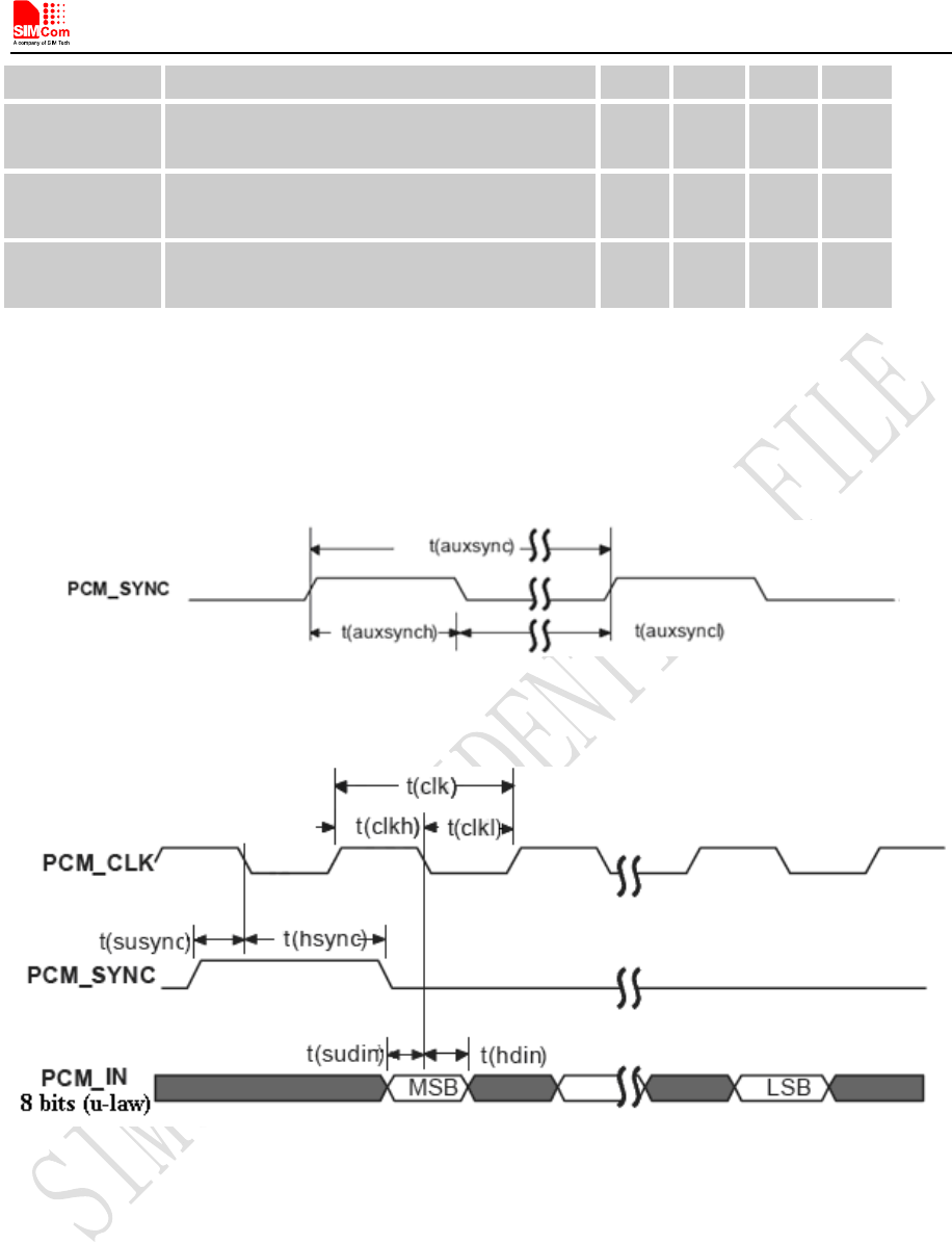
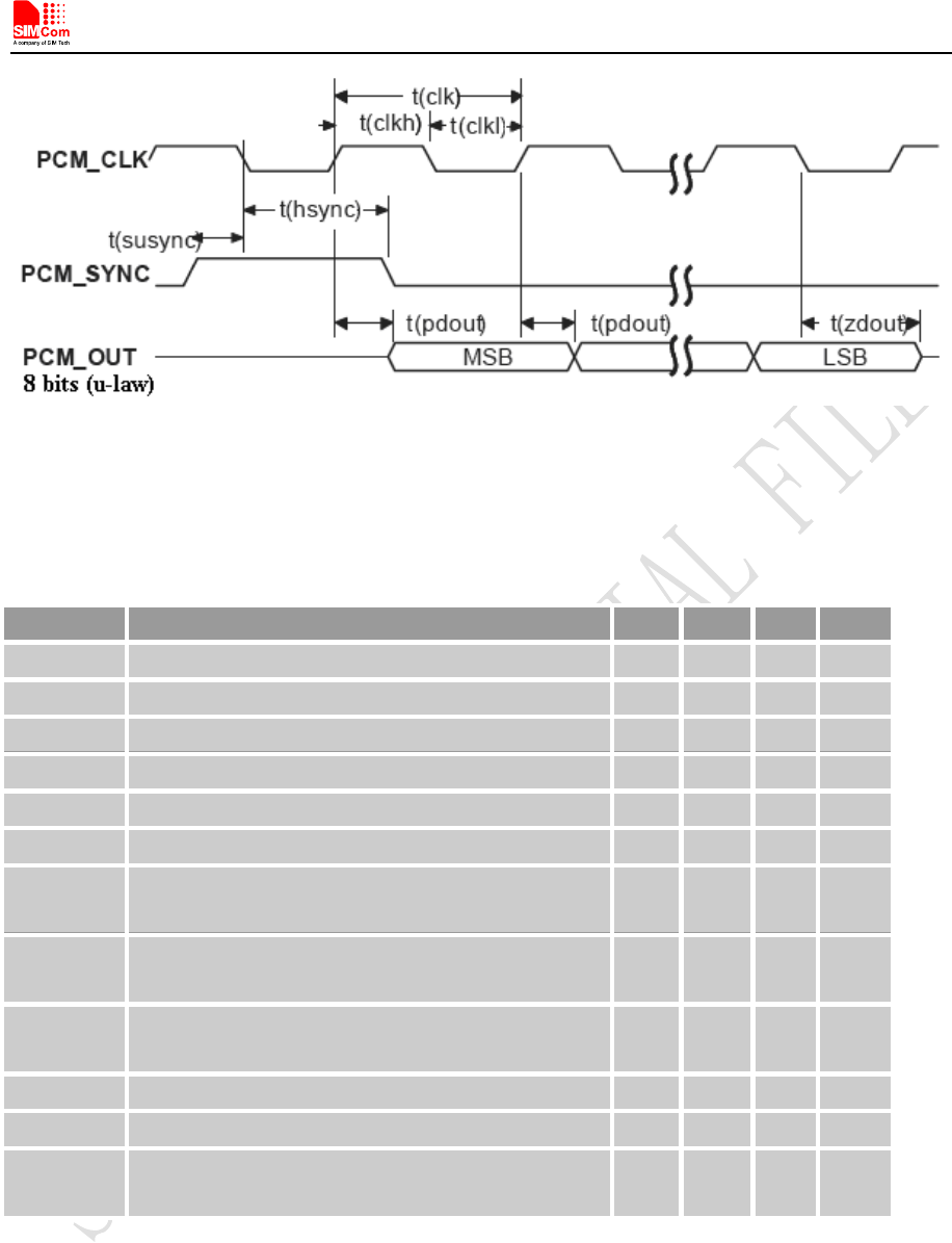
Primary PCM (2048 KHz PCM clock)
SIM5360A also supports 2.048 MHz PCM data and sync timing for -law codec. This is called the
primary PCM interface. User can use AT command to take the mode you want as discussed above.
Figure 31: Synchrony timing
Figure 32: EXT CODEC to MODULE timing
Smart Machine Smart Decision
SIM5360A_User_Manual_V1.03 2014-07-03
47
Figure 33: MODULE to EXT CODEC timing
Table 27: Timing parameters
Parameter Description Min Typ Max Unit
T(sync) PCM_SYNC cycle time – 125 – μs
T(synch) PCM_SYNC high time 400 500 – ns
T(syncl) PCM_SYNC low time – 124.5 – μs
T(clk) PCM_CLK cycle time – 488 – ns
T(clkh) PCM_CLK high time – 244 – ns
T(clkl) PCM_CLK low time – 244 – ns
T(susync) PCM_SYNC setup time high before falling edge of
PCM_CLK 60 – – ns
T(hsync) PCM_SYNC hold time after falling edge of
PCM_CLK 60 – – ns
T(sudin) PCM_IN setup time before falling edge of
PCM_CLK 50 – – ns
T(hdin) PCM_IN hold time after falling edge of PCM_CLK 10 – – ns
T(pdout) Delay from PCM_CLK rising to PCM_OUT valid – – 350 ns
T(zdout) Delay from PCM_CLK falling to PCM_OUT
HIGH-Z – 160 – ns
Note: SIM5360A can transmit PCM data by USB except for PCM interface.
3.11.3 Application Guide
The mode of SIM5360A PCM can be configured by AT command “AT+CPCM and AT+CPCMFMT”, and
the default configuration is master mode using short sync data format with 2.048MHz PCM_CLK and 8
kHz PCM_SYNC. Please refer to document [21] and document [1] for details.
Smart Machine Smart Decision
SIM5360A_User_Manual_V1.03 2014-07-03
48
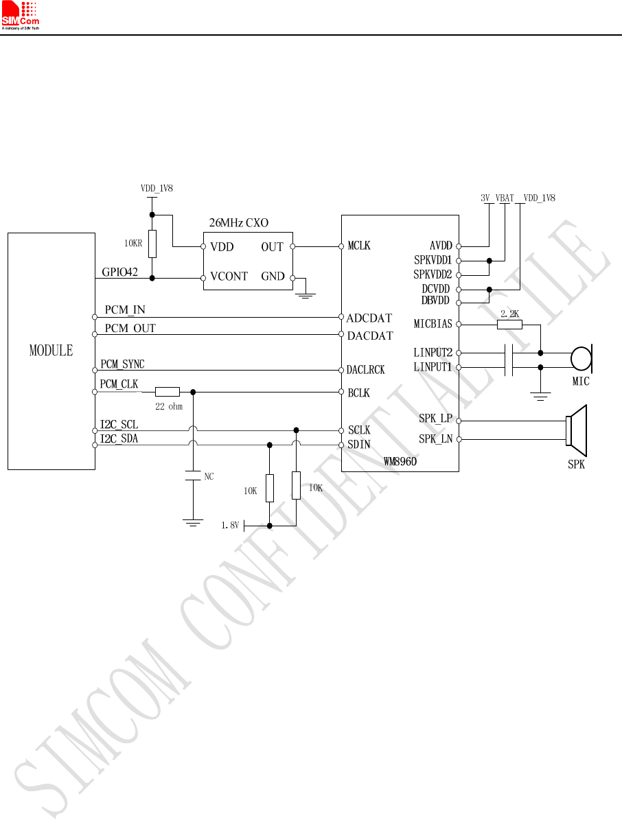
In addition, the firmware of SIM5360A has integrated the configuration on WM8960GEFL/RV codec
provided by WOLFSON MICROELECTRONICS with I2C interface.
The reference circuit of the reference design of PCM interfaces with external codec IC in the following
figure. It is recommended to use a 26MHz CXO component such as TXC CORPORATION
(www.txccorp.com) 8W26000011.
Figure 34: Reference Circuit of PCM Application with Audio Codec
3.12 GNSS (GPS and GLONASS)
SIM5360A merges GNSS (GPS/GLONASS) satellite and network information to provide a
high-availability solution that offers industry-leading accuracy and performance. This solution performs
well, even in very challenging environmental conditions where conventional GNSS receivers fail, and
provides a platform to enable wireless operators to address both location-based services and emergency
mandates.
3.12.1 Technical specification
Tracking sensitivity -159 dBm(GPS) -158 dBm(GLONASS)
Cold-start sensitivity -148 dBm
Accuracy (Open Sky) 2.5m (CEP50)
TTFF (Open Sky) Hot start <1s Cold start 35s
Receiver Type 16-channel, C/A Code
GPS L1 Frequency (1575.42±1.023MHz),
GLONASS: 1597.5~1605.8 MHz
Update rate Default 1 Hz

Smart Machine Smart Decision
SIM5360A_User_Manual_V1.03 2014-07-03
49
GNSS data format NMEA-0183
GNSS Current consumption (WCDMA/GSM Sleep mode) 100mA (Total supply current)
GNSS antenna Passive/Active antenna
Note: Performance will vary depending on the environment, antenna type and signal conditions and so
on.
3.12.2 Operate Mode
SIM5360A supports both A-GPS and S-GPS, and then provides three operating modes: mobile-assisted
mode, mobile-based mode and standalone mode. A-GPS includes mobile-assisted and mobile-based mode.
In mobile-assisted mode, when a request for position location is issued, available network information is
provided to the location server (e.g. Cell-ID) and assistance is requested from the location server. The
location server sends the assistance information to the handset. The handset/mobile unit measures the
GNSS observables and provides the GNSS measurements along with available network data (that is
appropriate for the given air interface technology) to the location server. The location server then
calculates the position location and returns results to the requesting entity.
In mobile-based mode, the assistant data provided by the location server encompasses not only the
information required to assist the handset in measuring the satellite signals, but also the information
required to calculate the handset’s position. Therefore, rather than provide the GNSS measurements and
available network data back to the location server, the mobile calculates the location on the handset and
passes the result to the requesting entity.
In standalone (autonomous) mode, the handset demodulates the data directly from the GNSS satellites.
This mode has some reduced cold-start sensitivity, and a longer time to first fix as compared to the assisted
modes. However, it requires no server interaction and works out of network coverage.
This combination of GNSS measurements and available network information provides:
● High-sensitivity solution that works in all terrains: Indoor, outdoor, urban, and rural
● High availability that is enabled by using both satellite and network information
Therefore, while network solutions typically perform poorly in rural areas and areas of poor cell
geometry/density, and while unassisted, GNSS-only solutions typically perform poorly indoors. The
SIM5360A GNSS solution provides optimal time to fix, accuracy, sensitivity, availability, and reduced
network utilization in both of these environments, depending on the given condition.
3.12.3 Application Guide
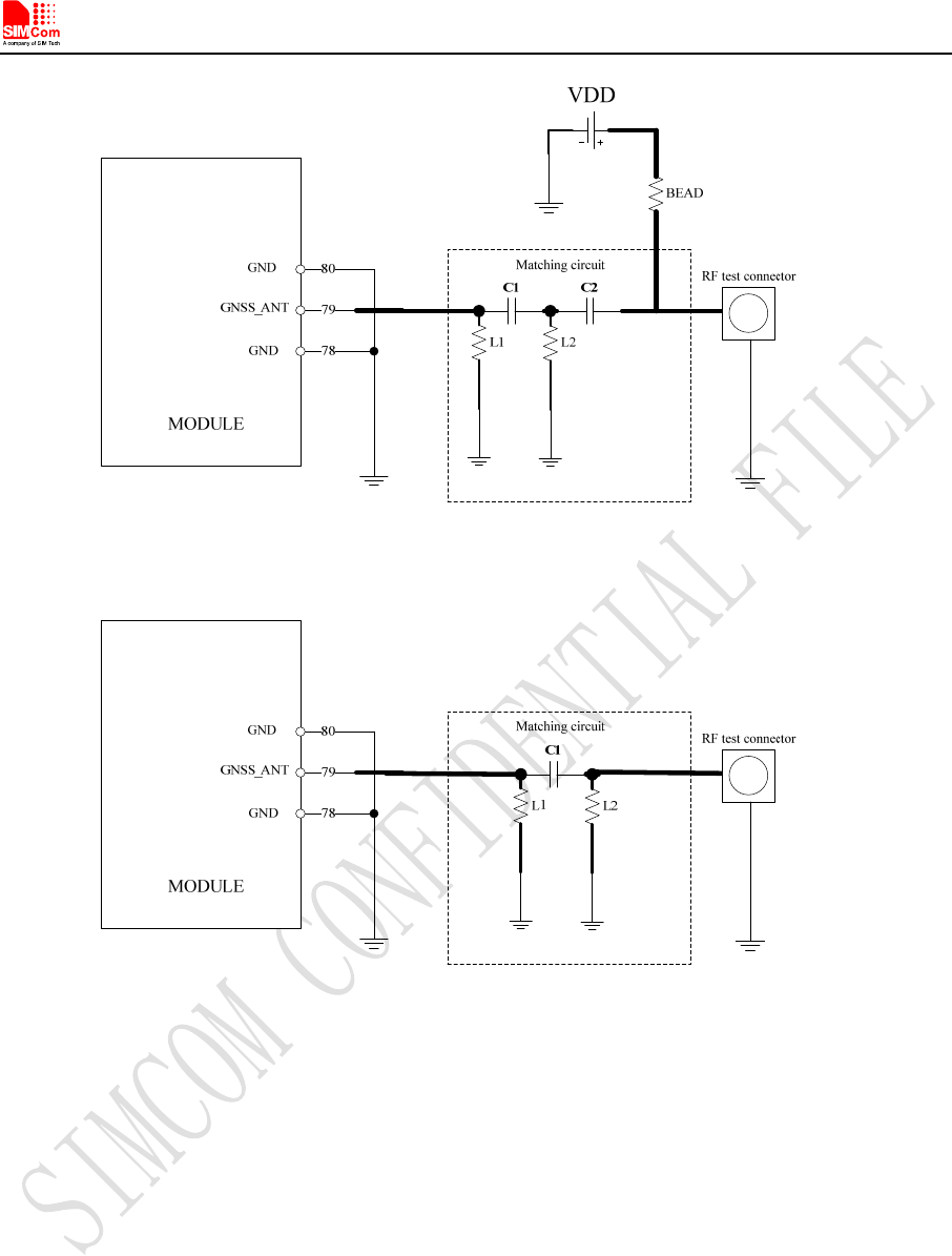
Users can adopt an active antenna or a passive antenna as GNSS signal transceiver. In this document, all
GNSS specification mentioned is from passive antenna. The following is the reference circuit.
Smart Machine Smart Decision
SIM5360A_User_Manual_V1.03 2014-07-03
50
Figure 35: Active antenna circuit
Figure 36:Passive antenna circuit (Default)
In above figures, the components C1 and L1, L2 are used for antenna matching, the values of the
components can only be obtained after the antenna tuning usually, and they are provided by antenna
vendor.C2 in Figure 36 is used for DC isolation. In active antenna circuit, users must use an external
LDO/DCDC to provide VDD voltage whose value should be taken according active antenna characteristic,
and VDD can be shut down to avoid consuming additional current when not being used.
GNSS can be used by NMEA port. User can select NMEA as output through UART or USB. NMEA
sentences are automatic and no command is provided. NMEA sentences include GSV, GGA, RMC, GSA,
and VTG. Before using GNSS, user should configure SIM5360A in proper operating mode by AT
command. Please refer to related document for details. SIM5360A can also get position location
information through AT directly.
Note: GNSS is closed by default, it could be started by AT+CGPS. The AT command has two parameters,
the first is on/off, and the second is GNSS mode. Default mode is standalone mode.
Smart Machine Smart Decision
SIM5360A_User_Manual_V1.03 2014-07-03
51
AGPS mode needs more support from the mobile telecommunication network. Refer to AGPS
application document for details.
3.13 Multi-functional interface
SIM5360A merges functions for various applications. It can enrich users’ design and lower the cost of
users’ hardware.
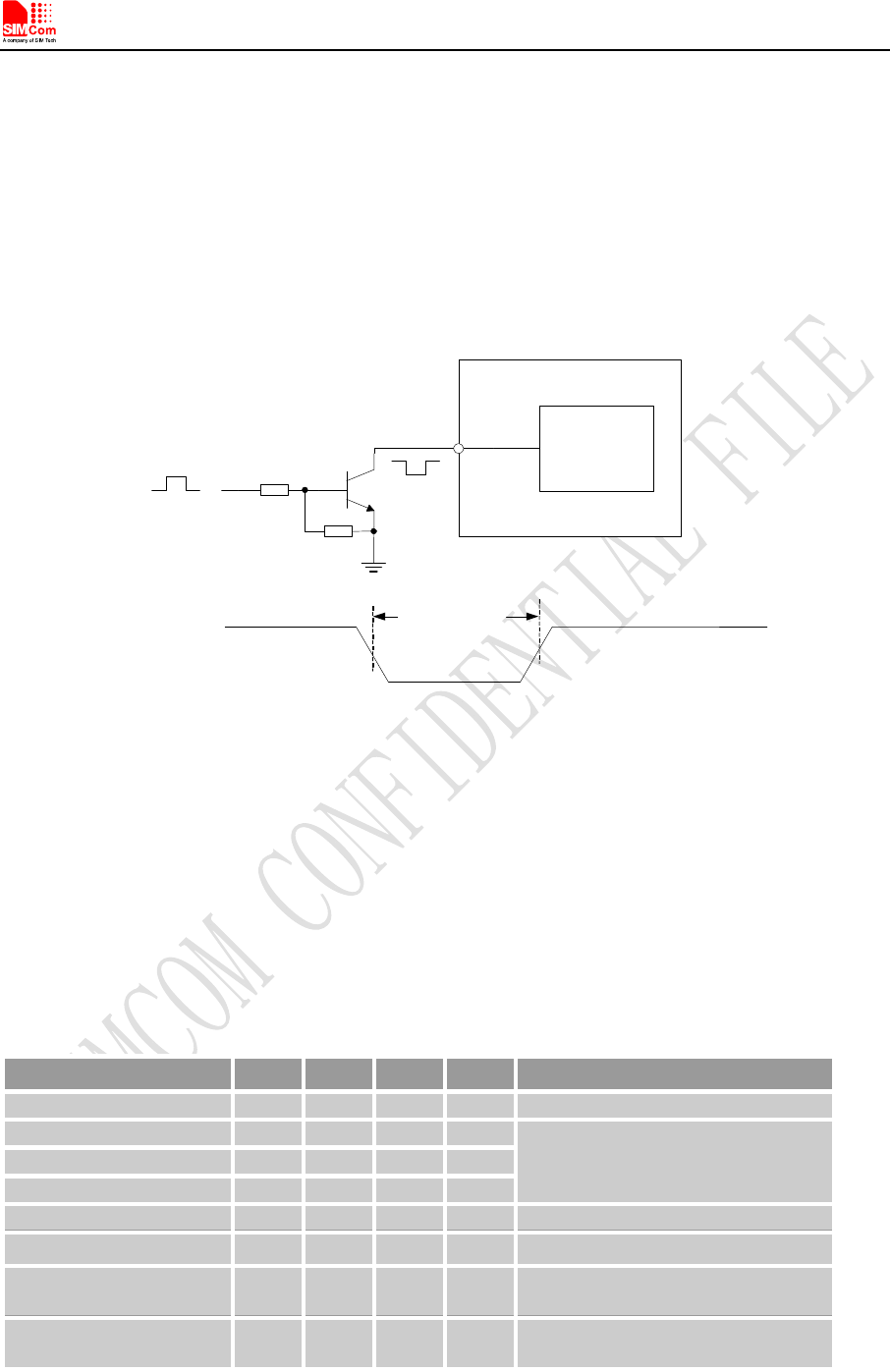
3.13.1 Sink Current Source
The dedicated pin (ISINK) is intended for driving passive devices,such as LCD backlight, this
implementation is VBAT tolerant and suitable for driving white LEDs. The high-current driver can
maintain a constant current which is set by the AT command “AT+ CLEDITST”, capable of up to 40 mA.
Table 28: Electronic characteristic
Symbol Description Min Typ Max Unit
ISINK Input voltage 0.5 VDD VBAT V
IO Input current 5 - 40 mA
Since the driver is ground-referenced current sink, the operating device it drives must form a current path
between the VDD pin and the ISINK pin. The following figure is for users reference.
MODULE
ISINK
Pin 45 is VBAT tolerant-
suitable for driving white
LEDs
Current Controls
Passive
device
+
-
VBAT
High
current
Figure 37: Current drive
Note: The sinking current can be adjusted to meet design requirement through the AT command “AT+
CLEDITST =<0>, <value>”.The “value” ranges from 0 to 15,on behalf of the current changes from
0mA to 150mA in steps of 10mA.
Smart Machine Smart Decision
SIM5360A_User_Manual_V1.03 2014-07-03
52
3.13.2 Reset Function
SIM5360A also have a RESET pin (PIN4) to reset the module. This function is used as an emergency reset
only when AT command “AT+CPOF” and the POWERKEY pin has no effect. User can pull the RESET
pin to ground, then the module will reset.
This pin is already pulled up in module, so the external pull-up resistor is not necessary. A 100nF capacitor
close to the RESET pin is strongly recommended. A reference circuit is recommended in the following
figure.
Treset >50ms
RESET
4.7K
47K
Reset Logic
MODULE
Reset Impulse
RESET
Figure 38: Reset circuit
Note
:
50ms<Treset<200ms. ESD components are suggested to be used on Reset pin.
3.13.3 ADC
SIM5360A has a dedicated ADC that is available for digitizing analog signals such as battery voltage and
so on; it is on PIN 47 and PIN 46 , namely ADC1 and ADC2 . This ADC is 15 bit
successive-approximation circuit, and electronic specification is shown in the following table.
Table 29: Electronic Characteristics
Specification Min Typ Max Unit Comments/Conditions
Resolution 15 Bits
Analog input bandwidth – 100 – kHz Analog Vdd = ADC reference
2.4MHz sample rate
Gain Error -2.5 +2.5 %
Offset Error -3.5 +3.5 LSB
Input Range GND 2.2V V
Input serial resistance 2 kΩ Sample and hold switch resistance
Power supply current
Normal operation 1.5 mA
Power supply current
Off 50 200 nA
User can introduce a signal in the ADC pin directly and use the AT command “AT+CADC” to get the raw

Smart Machine Smart Decision
SIM5360A_User_Manual_V1.03 2014-07-03
53
data which is between 0 and 32768. The data can be transformed to any type such as voltage, temperature
etc. Please refer to document [1].
Note: The input signal voltage value in ADC must not be higher than 2.2V.
3.13.4 LDO
SIM5360A has a LDO power output, namely VDD_EXT. The LDO is available and output voltage is
2.85v by default, rated for 300mA. User can switch the LDO on or off by the AT command
“AT+CVAUXS” and configure its output voltage by the AT command “AT+CVAUXV”.
Table 30: Electronic characteristic
Symbol Description Min Typ Max Unit
VDD_EXT Output voltage 1.5 2.85 3.05 V
IO Output current - - 300 mA

Smart Machine Smart Decision
SIM5360A_User_Manual_V1.03 2014-07-03
54
4 RF Specification
4.1 RF Specification
Table 31: Conducted transmission power
Frequency Max Min
GSM850 33dBm ±2dB 5dBm ± 5dB
PCS1900 30dBm ±2dB 0dBm ± 5dB
GSM850 (8-PSK) 27dBm ±3dB 5dBm ± 5dB
PCS1900(8-PSK) 26dBm +3/-4dB 0dBm ±5dB
WCDMA 1900 24dBm +1/-3dB -56dBm ±5dB
WCDMA 850 24dBm +1/-3dB -56dBm ±5dB
Table 32: Operating frequencies
Frequency Receiving Transmission
GSM850 869 ~894 MHz 824 ~849 MHz
PCS1900 1930~1990 MHz 1850~1910 MHz
WCDMA1900 1930~1990 MHz 1850~1910 MHz
WCDMA 850 869 ~894 MHz 824 ~849 MHz
Table 33: Conducted receive sensitivity
Frequency Receive sensitivity
GSM850 < -109dBm
PCS1900 < -109dBm
WCDMA 1900 < -110dBm
WCDMA 850 < -110dBm
4.2 Operating Specification
SIM5360A can support high rate data by GSM/WCDMA wireless network. In the different network
environment, data transmission rate shifts depending on modulation and encoding.
Table 34: GPRS/EDGE data throughout
Function Coding schemes 1 Timeslot 2 Timeslot 4 Timeslot
GPRS CS-1 9.05kbps 18.1kbps 36.2kbps
CS-2 13.4kbps 26.8kbps 53.6kbps
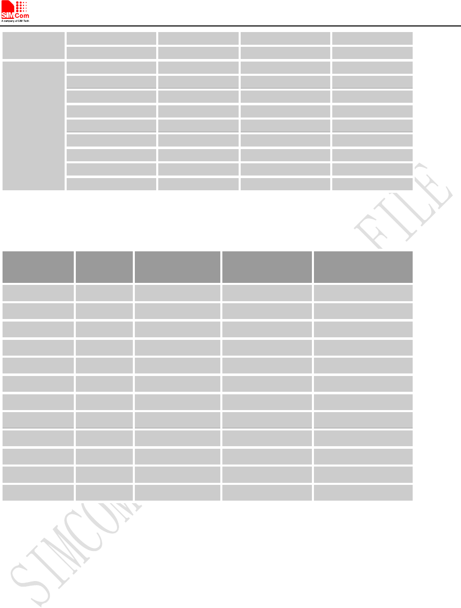
Smart Machine Smart Decision
SIM5360A_User_Manual_V1.03 2014-07-03
55
CS-3 15.6kbps 31.2kbps 62.4kbps
CS-4 21.4kbps 42.8kbps 85.6kbps
EDGE
MCS-1 8.80kbps 17.6kbps 35.20kbps
MCS-2 11.2kbps 22.4kbps 44.8kbps
MCS-3 14.8kbps 29.6kbps 59.2kbps
MCS-4 17.6kbps 35.2kbps 70.4kbps
MCS-5 22.4kbps 44.8kbps 89.6kbps
MCS-6 29.6kbps 59.2kbps 118.4kbps
MCS-7 44.8kbps 89.6kbps 179.2kbps
MCS-8 54.4kbps 108.8kbps 217.6kbps
MCS-9 59.2kbps 118.4kbps 236.8kbps
Table 35: HSDPA throughout
Category Supported Max supported
HS-DSCH codes
Theoretical max
peak rate(Mbps) Modulation
Category1 5 1.2 16QAM,QPSK
Category2 5 1.2 16QAM,QPSK
Category3 5 1.8 16QAM,QPSK
Category4 5 1.8 16QAM,QPSK
Category5 5 3.6 16QAM,QPSK
Category6 5 3.6 16QAM,QPSK
Category7 10 7.2 16QAM,QPSK
Category8 10 7.2 16QAM,QPSK
Category9 15 10.0 16QAM,QPSK
Category10 15 14.0 16QAM,QPSK
Category11 5 0.9 QPSK
Category12 5 1.8 QPSK
Note: Actual throughout rates depend on network configuration, network loading, signal condition and
so on.
4.3 Antenna Design Guide
There are three antenna ports for SIM5360A, Main antenna port named MAIN_ANT, Diversity antenna
port named DIV_ANT and GPS/GLONASS antenna port named GNSS_ANT, The RF interface of the
three antenna ports has an impedance of 50Ω.The maximum gain of the Main antenna gain should not
exceed 1dBi considering the SAR radio. No antenna gain may be used that would exceed the 2W EIRP
power limit in 1900MHz band.The input impendence of the antenna should be 50Ω, and the VSWR should
be less than 2.
SIMCom recommends that the total insertion loss between the antenna pad and antenna should meet the
following requirements:
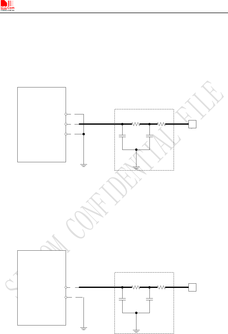
Smart Machine Smart Decision
SIM5360A_User_Manual_V1.03 2014-07-03
56
● GSM850<0.5dB
● PCS1900 <0.9dB
● WCDMA 1900<0.9dB
● WCDMA 850<0.5dB
To facilitate the antenna tuning and certification test, a RF connector and an antenna matching circuit
should be added. The following figure is the recommended circuit.
R2
C1
60
MODULE
59
MAIN_ANT
GND C2
58
GND
R1
Antenna feed pad
Matching circuit
J1
Figure 39: Antenna matching circuit (MAIN_ANT)
In this figure, the components R1,C1,C2 and R2 is used for antenna matching, the value of components
can only be got after the antenna tuning, usually, they are provided by antenna vendor. By default, the R1,
R2 are 0 ohm resistors, and the C1, C2 are reserved for tuning.
The RF test connector in the figure is used for the conducted RF performance test, and should be placed as
close as to the module’s antenna pin. The traces impedance between components must be controlled in
50ohm.
R5
C3
MODULE
82
DIV_ANT
GND C5
58
R3
Antenna feed pad
Matching circuit
J3
Figure 40: Antenna matching circuit (DIV_ANT)
In above figure, the components R3,C3,C5 and R5 is used for diversity antenna matching. The method of
antenna tuning is same as MAIN_ANT.

Smart Machine Smart Decision
SIM5360A_User_Manual_V1.03 2014-07-03
57
Contact us:
Shanghai SIMCom Wireless Solutions Ltd.
Add: SIM Technology Building, No.633, Jinzhong Road, Changning District, Shanghai P.R.
China 200335
Tel: +86 21 3235 3300
Fax: +86 21 3235 3301
URL: www.sim.com/wm