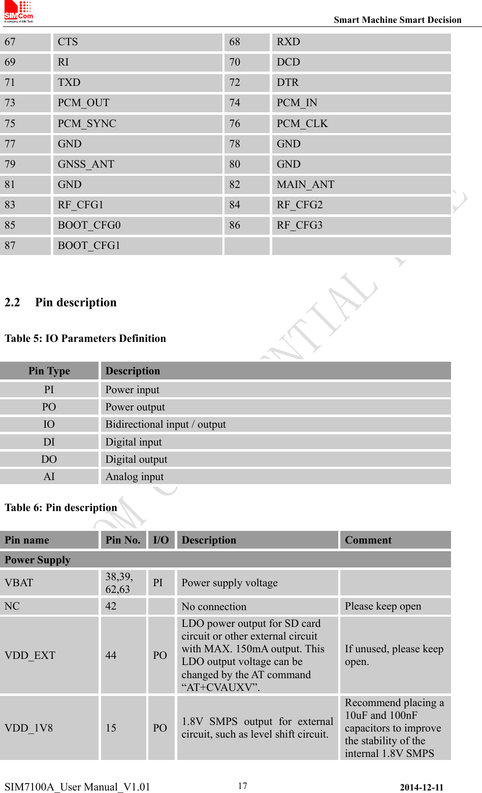
Simcom SIM7100A LTE/WCDMA Module User Manual UDV SIM7100A
Shanghai Simcom Ltd. LTE/WCDMA Module UDV SIM7100A
UserManual.wiki
>
Simcom
>
SIM7100A User Manual
>
UDV-SIM7100A_User Manual
Contents
1.
UDV-SIM7100A_User Manual
2.
UDV-SIM7100A_EVB_User Guide
UDV-SIM7100A_User Manual
Navigation menu
Upload a User Manual
Namespaces
Wiki Guide
HTML
PDF
Info
Views
User Manual
Discussion / Help
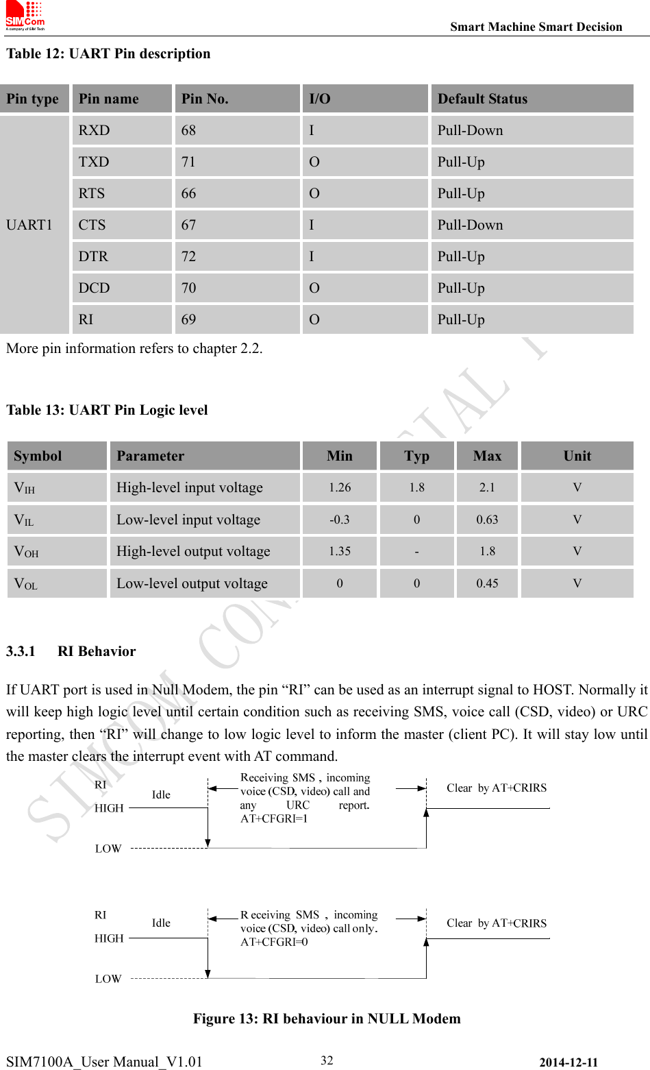
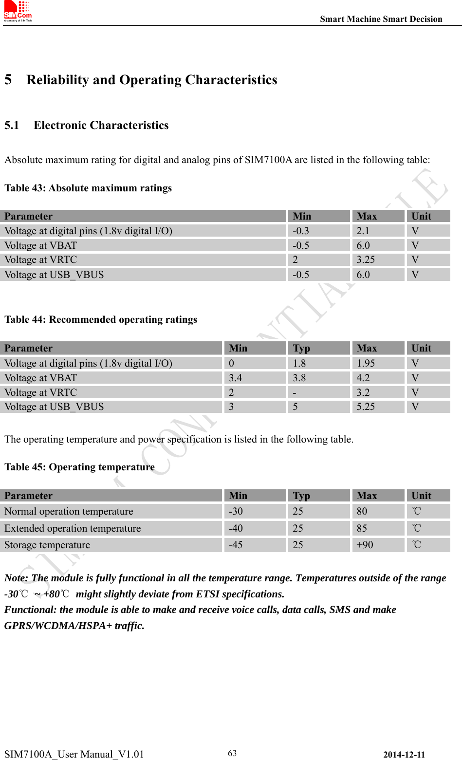
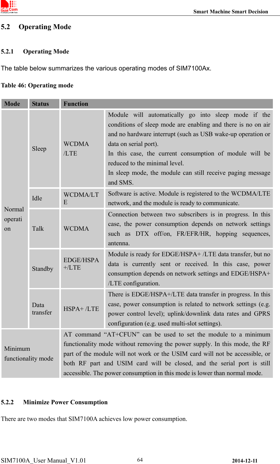
Navigation
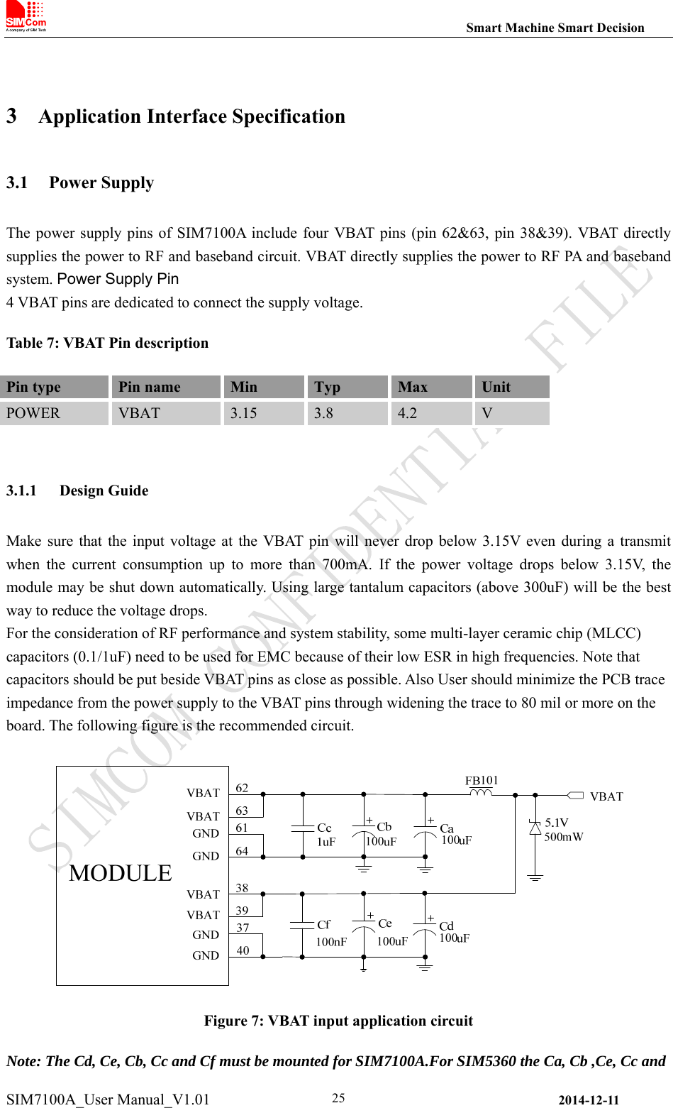
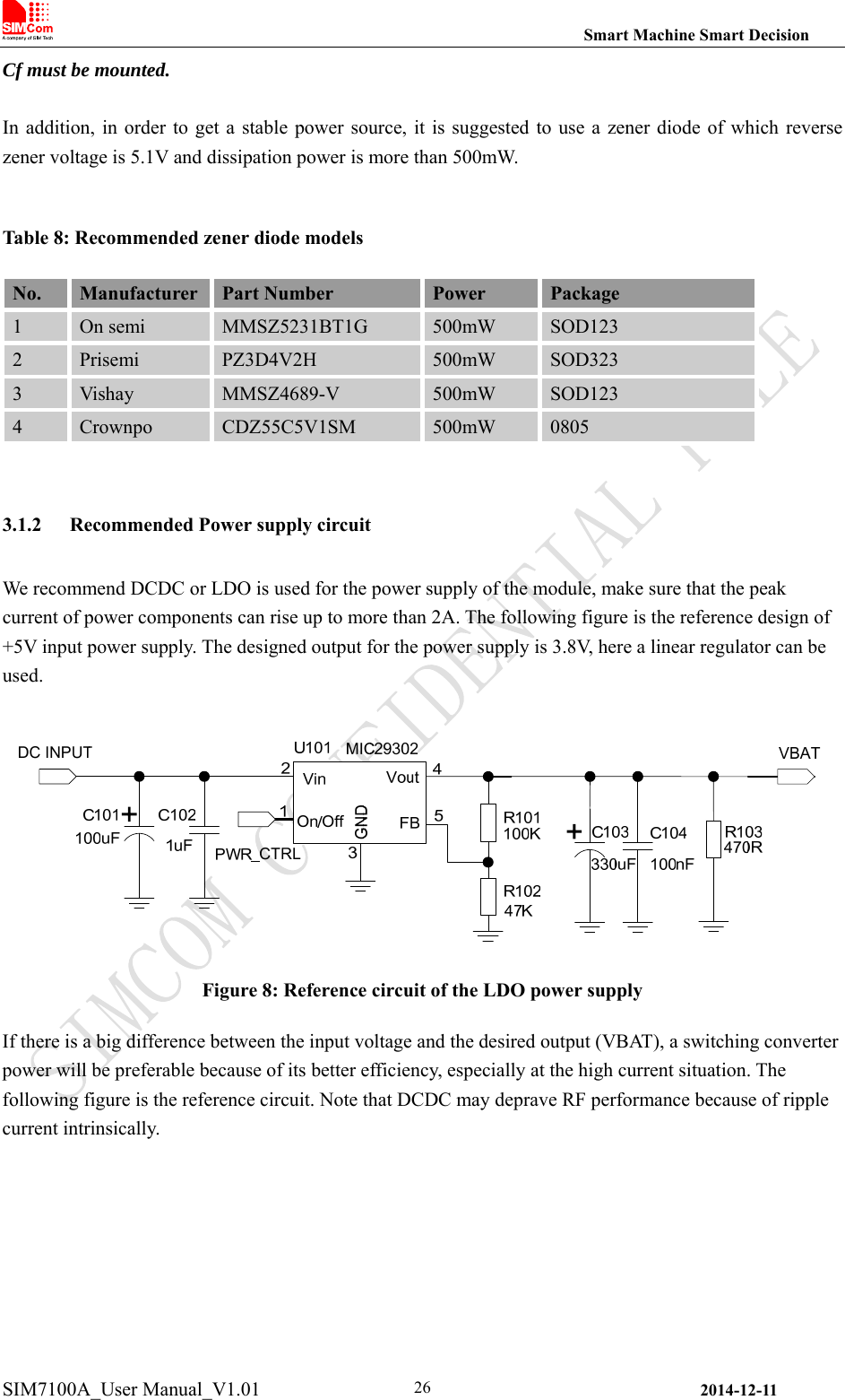
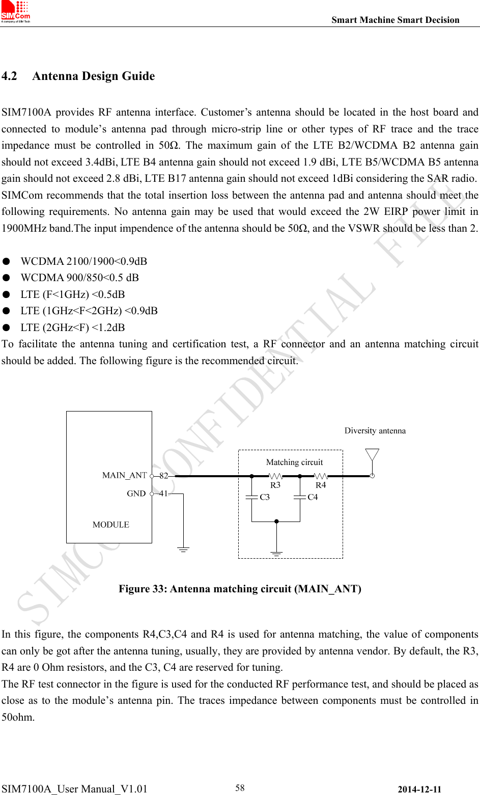
![Smart Machine Smart Decision SIM7100A_User Manual_V1.01 2014-12-11 27 Figure 9: Reference circuit of the DCDC power supply 3.1.3 Vol tage monitor To monitor the power supply voltage, user can use the AT command “AT+CBC”, this command has two parameters: the battery status and the voltage value (mV). It will return the capacity percentage and actual value of battery (at the VBAT pin). The voltage is continuously measured at intervals, whenever the measured battery voltage is lower than a specific value set by the AT command “AT+CVALARM”. For example, if the voltage value is set to be 3.4V, the following URC will be presented: “warning! voltage is low: 3.3v”. If the voltage is lower than a specific value which is set by the AT command “AT+CPMVT”, the module will be powered off automatically and AT commands cannot be executed any more. Note: Under-voltage warning function and under-voltage power-off function are disabled by default. For more information about these AT command, please refer to Document [1]. 3.2 Power on/Power off/Reset Time Sequence 3.2.1 Power on Sequence SIM7100A can be powered on by PWRKEY pin, which starts normal operating mode. PWRKEY pin is pulled up with a 200k ohm resistor to 1.8V in module. User can power on the SIM7100A by pulling the PWRKEY pin down for a short time. The power-on scenarios are illustrated in the following figures.](https://usermanual.wiki/Simcom/SIM7100A.UDV-SIM7100A-User-Manual/User-Guide-2482007-Page-27.png)
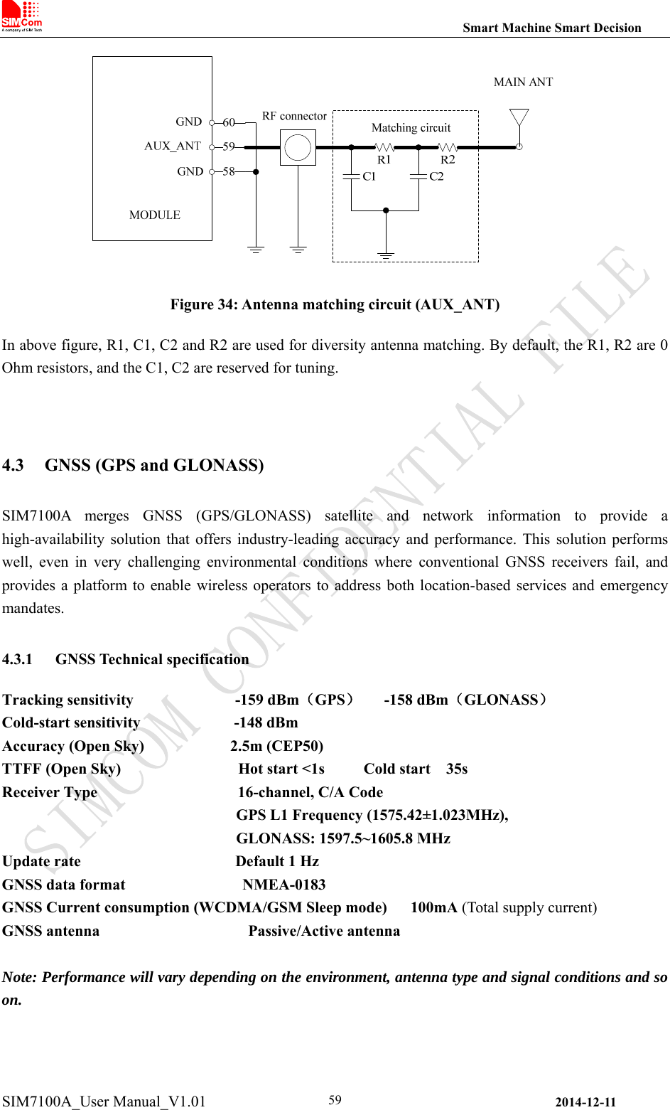
![Smart Machine Smart Decision SIM7100A_User Manual_V1.01 2014-12-11 29Table 9: Power on timing Symbol Parameter Time value UnitMin. Typ. Max. Ton The time to pull PWRKEY down to power on 180 500 - ms TpD+ The time to indicate connecting with the network - - 5 s Tpw+ The time to indicate the module is powered on completely - - 0.5 s Tuart The time to enable UART - - 8 s Tusb The time to enable USB - - 10 s Note: Module could be automatically power on by connecting PWRKEY pin to Low level directly. Before designing, please refer to Document [27] for more detail. 3.2.2 Power off Sequence The following methods can be used to power down SIM7100A. These procedures will make module disconnect from the network and allow the software to enter a safe state, and then save data before completely powering the module off. ● Method 1: Power off SIM7100A by pulling the PWRKEY pin down ● Method 2: Power off SIM7100A by AT command User can power off the SIM7100A by pulling PWRKEY down for a specific time. The power off scenario is illustrated in the following figure.](https://usermanual.wiki/Simcom/SIM7100A.UDV-SIM7100A-User-Manual/User-Guide-2482007-Page-29.png)
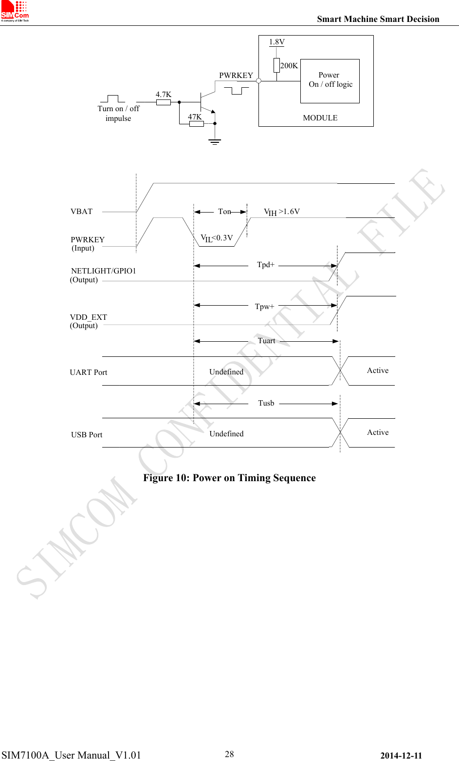
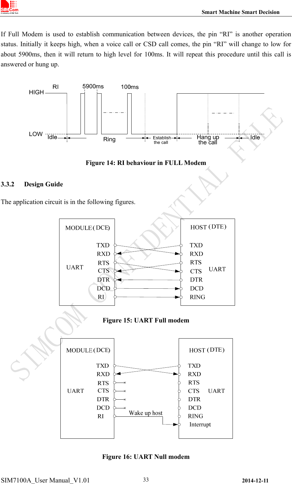
![Smart Machine Smart Decision SIM7100A_User Manual_V1.01 2014-12-11 30NETLIGHT/GPIO1(Output)VIL<0.3VToffPWRKEY( Input )Tpd-UART Port UndefinedActiveUSB Port UndefinedActiveVDD_EXT(Output )Tpw-TuartTusbVIL<0.3VTonTrestart Figure 11: Power off timing sequence Table 10: Power off timing Symbol Parameter Time value Min. Typ. Max. UnitToff The time pulling PWRKEY down to power off 0.5 - 5 s TpD- The time to indicate disconnecting from the network - - 2 s Tpw- The time to indicate the module power off completely - - 2 s Tuart The time to disable UART - - 3 s Tusb The time to disable USB - - 2 s Trestart The time to power on again after Tpw- 0 - - s User can also use the AT command “AT+C POF ” to power down the module. After that, the AT commands cannot be executed any longer. The module enters the POWER DOWN mode. VDD_EXT pin can be used to detect whether module is powered on or not. When module is powered on and firmware goes ready, VDD_EXT will be high level. Note: For details about “AT+CPOF”, please refer to Document [1]. 3.2.3 Reset Function SIM7100A also have a RESET pin (PIN4) to reset the module. This function is used as an emergency reset](https://usermanual.wiki/Simcom/SIM7100A.UDV-SIM7100A-User-Manual/User-Guide-2482007-Page-30.png)
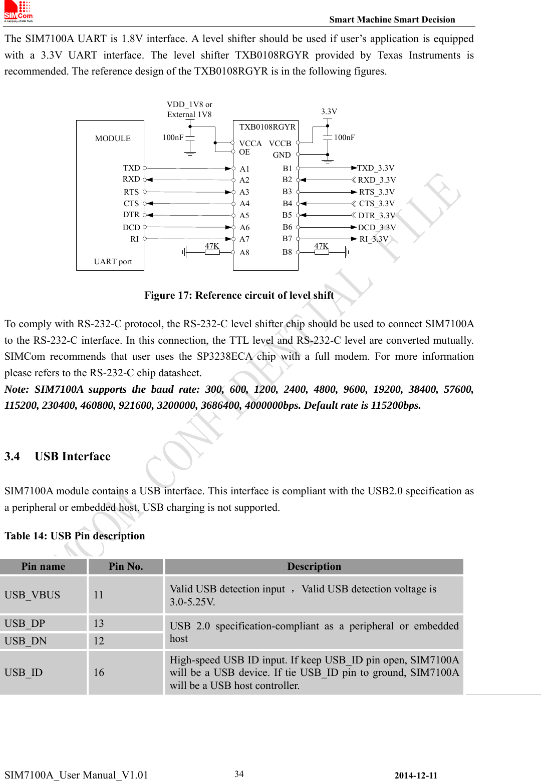
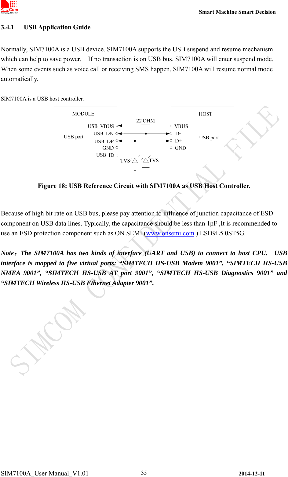
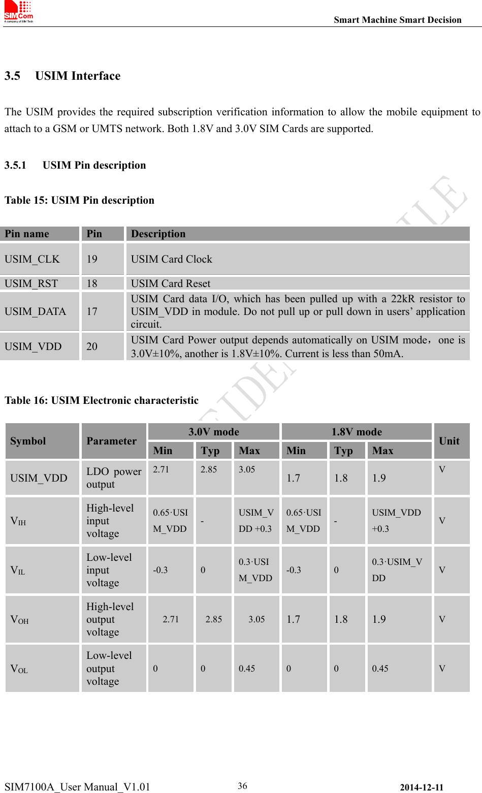
![Smart Machine Smart Decision SIM7100A_User Manual_V1.01 2014-12-11 373.5.2 USIM Application Guide It is recommended to use an ESD protection component such as ST (www.st.com ) ESDA6V1W5 or ON SEMI (www.onsemi.com ) SMF05C. Note that the SIM peripheral circuit should be close to the SIM card socket. The reference circuit of the 6-pin SIM card holder is illustrated in the following figure. Figure 19: USIM interface reference circuit Note: USIM_DATA has been pulled up with a 15kohm resistor to USIM_VDD in module. A 220nF shut capacitor on USIM_VDD is used to reduce interference. Use AT Commands to get information in USIM card. For more detail, please refer to document [1]. 3.5.3 Recommend Components of USIM holder For 6 pins USIM socket, SIMCom recommend to use Amphenol C707 10M006 512. User can visit http://www.amphenol.com for more information about the holder.](https://usermanual.wiki/Simcom/SIM7100A.UDV-SIM7100A-User-Manual/User-Guide-2482007-Page-37.png)
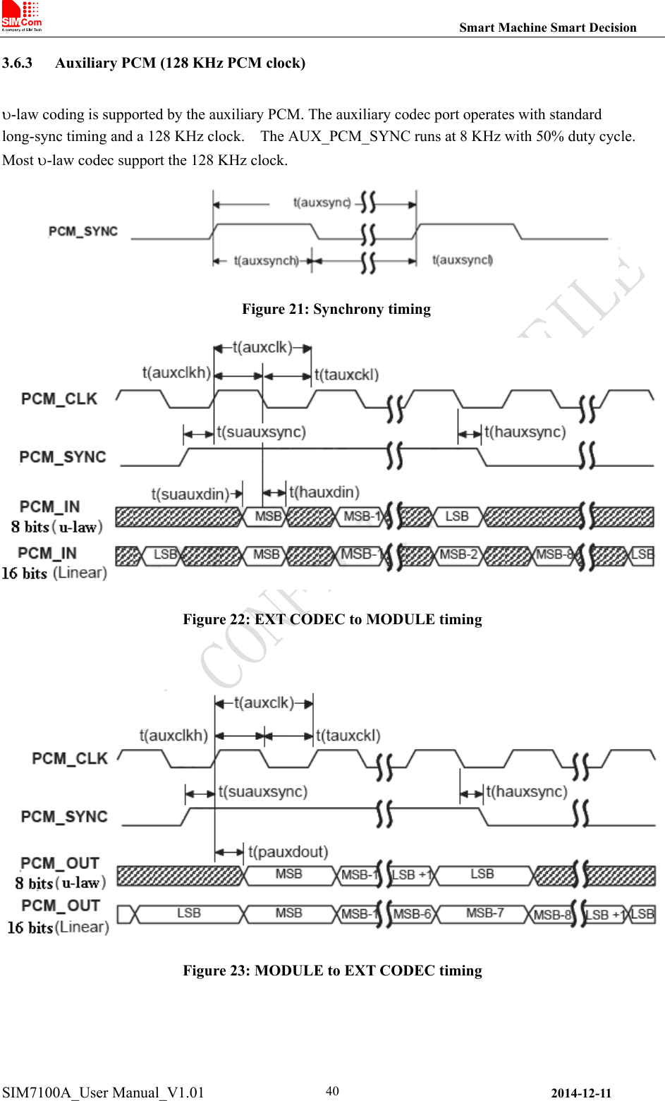
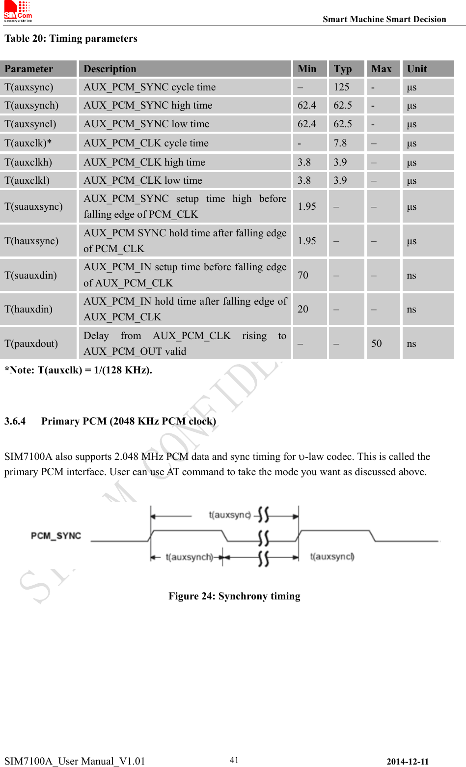
![Smart Machine Smart Decision SIM7100A_User Manual_V1.01 2014-12-11 39SIM7100A is always a master. SIM7100A also supports 3 kinds of coding formats: 8 bits (-law or A-law) and 16 bits (linear). Note: PCM interface is multiplexed from GPIO (default setting). The AT command “AT+CPCM” is used to switch between PCM and GPIO functions. Please refer to document [21] and document [1] for details. 3.6.1 PCM Pin Description Table 18: PCM Pin description Pins Pin No. Description PCM_OUT 73 PCM data output PCM_IN 74 PCM data input PCM_SYNC 75 PCM data synchrony PCM_CLK 76 PCM data clock Table 19: PCM Electronic characteristic Symbol Parameter Min Typ Max Unit VIH High-level input voltage 1.26 1.8 2.1 V VIL Low-level input voltage -0.3 0 0.63 V VOH High-level output voltage 1.35 - 1.8 V VOL Low-level output voltage 0 0 0.45 V 3.6.2 PCM Signal Description The default PCM interface in SIM7100A is the auxiliary PCM interface. The data changes on the high level of PCM_CLK and is sampled at the falling edge of PCM_CLK in one period. Primary PCM is disabled after every power-on or every reset event. So user must use AT command to enable the primary PCM mode after powering on or resetting the module every time if user wants to use Primary PCM.SIM7100A PCM Interface can be operated in Master or Slave mode if it is configured to primary PCM. In Master Mode, the Module drives the clock and sync signals that are sent to the external codec. When it is in Slave Mode, the external codec drives the clock and sync signals which are sent to the module. Both PCM modes are discussed in this section followed by additional PCM topics.](https://usermanual.wiki/Simcom/SIM7100A.UDV-SIM7100A-User-Manual/User-Guide-2482007-Page-39.png)
![Smart Machine Smart Decision SIM7100A_User Manual_V1.01 2014-12-11 43T(sudin) PCM_IN setup time before falling edge of PCM_CLK 50 – – ns T(hdin) PCM_IN hold time after falling edge of PCM_CLK 10 – – ns T(pdout) Delay from PCM_CLK rising to PCM_OUT valid – – 350 ns T(zdout) Delay from PCM_CLK falling to PCM_OUT HIGH-Z – 160 – ns Note: SIM7100A can transmit PCM data by USB except for PCM interface. 3.6.5 PCM Application Guide The mode of SIM7100A PCM can be configured by AT command “AT+CPCM and AT+CPCMFMT”, and the default configuration is master mode using short sync data format with 2.048MHz PCM_CLK and 8 kHz PCM_SYNC. Please refer to document [21] and document [1] for details. In addition, the firmware of SIM7100A has integrated the configuration on WM8960GEFL/RV codec provided by WOLFSON MICROELECTRONICS with I2C interface. The reference circuit of the reference design of PCM interfaces with external codec IC in the following figure. It is recommended to use a 26MHz CXO component such as TXC CORPORATION (www.txccorp.com) 8W26000011. Figure 27: Reference Circuit of PCM Application with Audio Codec](https://usermanual.wiki/Simcom/SIM7100A.UDV-SIM7100A-User-Manual/User-Guide-2482007-Page-43.png)
![Smart Machine Smart Decision SIM7100A_User Manual_V1.01 2014-12-11 48If these pins are configured for GPIOs, the sequence is listed in the following table. Table 28: Keypad multiplexing function Pin name Pin number Mode 0(default) Mode 1 KBR4 34 KBR4 GPIO6 KBR3 35 KBR3 GPIO7 KBR2 30 KBR2 GPIO8 KBR1 33 KBR1 GPIO9 KBR0 29 KBR0 GPIO10 KBC4 36 KBC4 GPIO11 KBC3 32 KBC3 GPIO12 KBC2 31 KBC2 GPIO13 KBC1 27 KBC1 GPIO14 KBC0 28 KBC0 GPIO15 Note: Refer to document [23] for detailed information of Keypad Application Note. 3.10 SPI Interface SPI interface of SIM7100A is master only. It provides a duplex, synchronous, serial communication link with peripheral devices. Its operation voltage is 1.8V, with clock rates up to 26 MHz. 3.10.1 SPI Pin Description Table 29: SPI Pin description Table 30: SPI Electronic characteristic Symbol Parameter Min Typ Max Unit VIH High-level input voltage 1.26 1.8 2.1 V Pin name Pin No. Function SPI_CS 9 SPI chip-select; not mandatory in a point-to-point connection SPI_MISO 7 SPI master in/slave out data SPI_CLK 6 SPI clock SPI_MOSI 8 SPI master out/slave in data](https://usermanual.wiki/Simcom/SIM7100A.UDV-SIM7100A-User-Manual/User-Guide-2482007-Page-48.png)
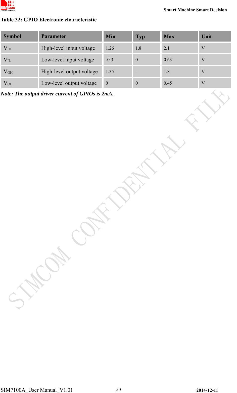
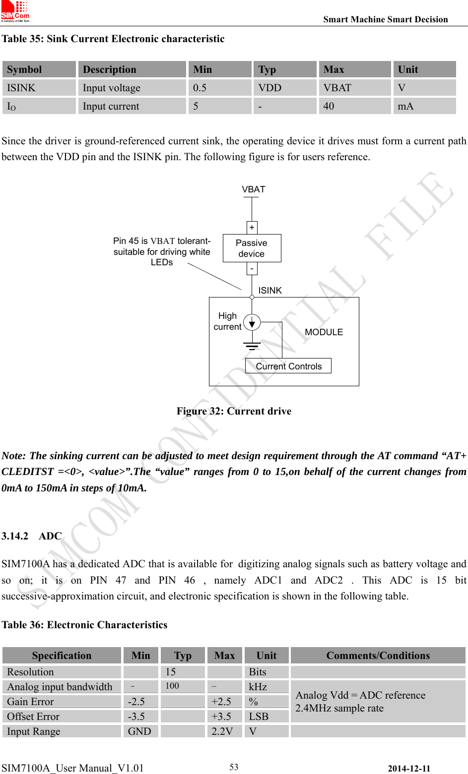
![Smart Machine Smart Decision SIM7100A_User Manual_V1.01 2014-12-11 52 Figure 31: Flight mode switch Table 34: Flight mode status GPIO4 Status Module operation Low Level Flight Mode: RF is closed. High Level Normal Mode: RF is working. Note:1. For SIM7100A, GPIO0, GPIO2, GPIO3 and GPIO5 have multiplex function, user can use them as PCM interface to connect extend codec. Refer to section 3.11 and document [1] for details. 2. When the module is powered off, make sure all digital interfaces (PCM UART, etc) connected with peripheral devices have no voltage higher than 0.3V. If users’ design cannot meet above conditions, high level voltages maybe occur in GPIO pins because current leakage from above digital interfaces may occur. 3.14 Multi-functional interface SIM7100A merges functions for various applications. It can enrich users’ design and lower the cost of users’ hardware. 3.14.1 Sink Current Source The dedicated pin (ISINK) is intended for driving passive devices,such as LCD backlight, this implementation is VBAT tolerant and suitable for driving white LEDs. The high-current driver can maintain a constant current which is set by the AT command “AT+ CLEDITST”, capable of up to 40 mA.](https://usermanual.wiki/Simcom/SIM7100A.UDV-SIM7100A-User-Manual/User-Guide-2482007-Page-52.png)
![Smart Machine Smart Decision SIM7100A_User Manual_V1.01 2014-12-11 54Input serial resistance 2 kΩ Sample and hold switch resistance Power supply current Normal operation 1.5 mA Power supply current Off 50 200 nA User can introduce a signal in the ADC pin directly and use the AT command “AT+CADC” to get the raw data which is between 0 and 32768. The data can be transformed to any type such as voltage, temperature etc. Please refer to document [1]. Note: The input signal voltage value in ADC must not be higher than 2.2V. 3.14.3 LDO SIM7100A has a LDO power output, namely VDD_EXT. The LDO is available and output voltage is 2.85v by default, rated for 150mA. User can switch the LDO on or off by the AT command “AT+CVAUXS” and configure its output voltage by the AT command “AT+CVAUXV”. Table 37: Electronic characteristic Symbol Description Min Typ Max Unit VDD_EXT Output voltage 1.7 2.85 3.05 V IO Output current - - 50 mA](https://usermanual.wiki/Simcom/SIM7100A.UDV-SIM7100A-User-Manual/User-Guide-2482007-Page-54.png)
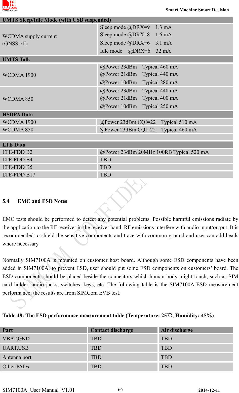
![Smart Machine Smart Decision SIM7100A_User Manual_V1.01 2014-12-11 655.2.3 Sleep mode If peripheral equipments stops working, and there is no on air or hardware interrupts (such as GPIO interrupts or data on UART), SIM7100A will enter sleep mode automatically. In this mode, SIM7100A can still receive paging,voice call or SMS from network. If USB interface of SIM7100A is connected to host CPU, but host CPU does not support USB suspending, then SIM7100A will not enter sleep mode. After USB is disconnected, SIM7100A will enter sleep mode. Note: When UART interface is connected with host CPU, SIM7100A cannot enter sleep mode until RXD is pulled down by the host CPU. If the module is in the idle mode, make sure to pull the RXD to low level by host CPU. SIMCom recommends using GPIO43 or DTR to wake up the module from host CPU and to use GPIO41 or RI to wake up the host CPU. Before designing, pay attention to how to realize waking function and refer to Document[24] and Document[25] for more detail. 5.2.4 Minimum functionality mode Minimum functionality mode ceases a majority function of module, thus minimizing the power consumption. This mode is set by the AT command which provides a choice of the functionality levels. ● AT+CFUN=0: Minimum functionality ● AT+CFUN=1: Full functionality (Default) ● AT+CFUN=4: Disable RF function of the module (Flight mode) If SIM7100A has been set to minimum functionality mode, the module will firstly enter sleep mode, then the RF function and SIM card function will be closed. In this case, the serial port is still accessible, but RF function or SIM card will be unavailable. When SIM7100A is in minimum functionality or flight mode, it can return to full functionality by the AT command “AT+CFUN=1”. 5.3 Current Consumption The current consumption in suspended mode and without USB connection is listed in the table below. Here, “suspended mode” means that SIM7100A is connected to USB bus, but it does not transfer data. Table 47: Current consumption OFF state OFF state supply current Power down 10uA UMTS Sleep/Idle Mode (without USB connection) WCDMA supply current (GNSS off) Sleep mode@DRX=9 1.1 mA Sleep mode @DRX=8 1.3 mA Sleep mode @DRX=6 2.8 mA Idle mode @DRX=6 15 mA](https://usermanual.wiki/Simcom/SIM7100A.UDV-SIM7100A-User-Manual/User-Guide-2482007-Page-65.png)
![Smart Machine Smart Decision SIM7100A_User Manual_V1.01 2014-12-11 68 Figure 38: The ramp-soak-spike reflow profile of SIM7100A For details about secondary SMT, please refer to document [26]. 6.3 Moisture Sensitivity Level (MSL) SIM7100A is qualified to Moisture Sensitivity Level (MSL) 5 in accordance with JEDEC J-STD-033. After the prescribed time limit exceeded, users should bake modules for 192 hours in drying equipment (<5% RH) at 40° C +5° C/-0° C, or 72 hours at 85° C +5° C/-5° C. Note that plastic tray is not heat-resistant, users must not use the tray to bake at 85° C or the tray may be damaged. Table 49: Moisture sensitivity level and floor life Moisture Sensitivity Level (MSL) Floor Life (out of bag) at factory ambient≤30°C/60% RH or as stated 1 Unlimited at ≦30℃/85% RH 2 1 year 2a 4 weeks 3 168 hours 4 72 hours 5 48 hours 5a 24 hours 6 Mandatory bake before use. After bake, it must be reflowed within the time limit specified on the label. NOTE: For product handling, storage, processing, IPC / JEDEC J-STD-033 must be followed.](https://usermanual.wiki/Simcom/SIM7100A.UDV-SIM7100A-User-Manual/User-Guide-2482007-Page-68.png)
![Smart Machine Smart Decision SIM7100A_User Manual_V1.01 2014-12-11 71 B. SIM7100A GPIOs List Table 50: SIM7100A GPIOs list Name GPIO Index Default Function Alternate Function PCM_IN 0 GPIO Interrupt [LEVEL/LOW] PCM_IN STATUS_LED 1 Status led GPIO1 PCM_SYNC 2 GPIO [IN] PCM_SYNC PCM_CLK 3 GPIO [OUT/LOW] PCM_CLK RF_SWITCH 4 RF Switch GPIO4 PCM_OUT 5 GPIO [OUT/LOW] PCM_OUT KBR4 6 Keypad GPIO KBR3 7 Keypad GPIO KBR2 8 Keypad GPIO KBR1 9 Keypad GPIO KBR0 10 Keypad GPIO KBC4 11 Keypad GPIO KBC3 12 Keypad GPIO KBC2 13 Keypad GPIO KBC1 14 Keypad GPIO KBC0 15 Keypad GPIO CTS 33 CTS GPIO RTS 34 RTS GPIO DTR 35 DTR wake up module GPIO DCD 36 DCD GPIO RI 37 RI wake up host GPIO GPIO40 40 Module power up status GPIO GPIO41 41 Wake up host GPIO GPIO42 42 GPIO[OUT/LOW] GPIO GPIO43 43 Wake up module GPIO GPIO44 44 GPIO[OUT/LOW] GPIO C. Digital I/O Characteristics Table 51: Digital I/O characteristics Parameter Description 1.8V Digital I/O Unit Min Typ Max VIH High-level input voltage 1.26 1.8 2.1 V VIL Low-level input voltage -0.3 0 0.63 V VOH High-level output 1.35 - 1.8 V](https://usermanual.wiki/Simcom/SIM7100A.UDV-SIM7100A-User-Manual/User-Guide-2482007-Page-71.png)
![Smart Machine Smart Decision SIM7100A_User Manual_V1.01 2014-12-11 72voltage VOL Low-level output voltage 0 0 0.45 V IOH High-level output current - 1 - mA IOL Low-level output current - -1 - mA IIH Input high leakage current - - 1 uA IIL Input low leakage current -1 - - uA CIN Input capacitance - - 7 pF Note: These parameters are for digital interface pins, such as keypad, GPIO, I2C, UART, SPI. Digital I/O specifications under both conditions are presented in the above tables. D. Related Documents Table 52: Related documents SN Document name Remark [1] SIM7100A_ATC_V1.00 SIM7100A_ATC_V1.00 [2] ITU-T Draft new recommendationV.25ter Serial asynchronous automatic dialing and control [3] GSM 07.07 Digital cellular telecommunications (Phase 2+); AT command set for GSM Mobile Equipment (ME) [4] GSM 07.10 Support GSM 07.10 multiplexing protocol [5] GSM 07.05 Digital cellular telecommunications (Phase 2+); Use of Data Terminal Equipment – Data Circuit terminating Equipment (DTE – DCE) interface for Short Message Service (SMS) and Cell Broadcast Service (CBS) [6] GSM 11.14 Digital cellular telecommunications system (Phase 2+); Specification of the SIM Application Toolkit for the Subscriber Identity Module – Mobile Equipment (SIM – ME) interface [7] GSM 11.11 Digital cellular telecommunications system (Phase 2+); Specification of the Subscriber Identity Module – Mobile Equipment (SIM – ME) interface [8] GSM 03.38 Digital cellular telecommunications system (Phase 2+); Alphabets and language-specific information [9] GSM 11.10 Digital cellular telecommunications system (Phase 2); Mobile Station (MS) conformance specification; Part 1: Conformance specification [10] 3GPP TS 51.010-1 Digital cellular telecommunications system (Release 5); Mobile Station (MS) conformance specification](https://usermanual.wiki/Simcom/SIM7100A.UDV-SIM7100A-User-Manual/User-Guide-2482007-Page-72.png)
![Smart Machine Smart Decision SIM7100A_User Manual_V1.01 2014-12-11 73[11] 3GPP TS 34.124 Electromagnetic Compatibility (EMC) for mobile terminals and ancillary equipment. [12] 3GPP TS 34.121 Electromagnetic Compatibility (EMC) for mobile terminals and ancillary equipment. [13] 3GPP TS 34.123-1 Technical Specification Group Radio Access Network; Terminal conformance specification; Radio transmission and reception (FDD) [14] 3GPP TS 34.123-3 User Equipment (UE) conformance specification; Part 3: Abstract Test Suites. [15] EN 301 908-02 V2.2.1 Electromagnetic compatibility and Radio spectrum Matters (ERM); Base Stations (BS) and User Equipment (UE) for IMT-2000. Third Generation cellular networks; Part 2: Harmonized EN for IMT-2000, CDMA Direct Spread (UTRA FDD) (UE) covering essential requirements of article 3.2 of the R&TTE Directive [16] EN 301 489-24 V1.2.1 Electromagnetic compatibility and Radio Spectrum Matters (ERM); Electromagnetic Compatibility (EMC) standard for radio equipment and services; Part 24: Specific conditions for IMT-2000 CDMA Direct Spread (UTRA) for Mobile and portable (UE) radio and ancillary equipment [17] IEC/EN60950-1(2001) Safety of information technology equipment (2000) [18] 3GPP TS 51.010-1 Digital cellular telecommunications system (Release 5); Mobile Station (MS) conformance specification [19] GCF-CC V3.23.1 Global Certification Forum - Certification Criteria [20] 2002/95/EC Directive of the European Parliament and of the Council of 27 January 2003 on the restriction of the use of certain hazardous substances in electrical and electronic equipment (RoHS) [21] Audio Application Note V1.01 Audio Application Note V1.01 [22] Reserved Reserved [23] Keypad Application Note V1.01 Keypad Application Note V1.01 [24] Sleep_Application_Note Sleep_Application_Note [25] Waking_up_Application_Note Waking_up_Application_Note [26] Module secondary-SMT-UGD SMT Note [27] SIM5xxx_Automatic_POWER_ON_Application_Note SIM5xxx_Automatic_POWER_ON_Application_Note](https://usermanual.wiki/Simcom/SIM7100A.UDV-SIM7100A-User-Manual/User-Guide-2482007-Page-73.png)