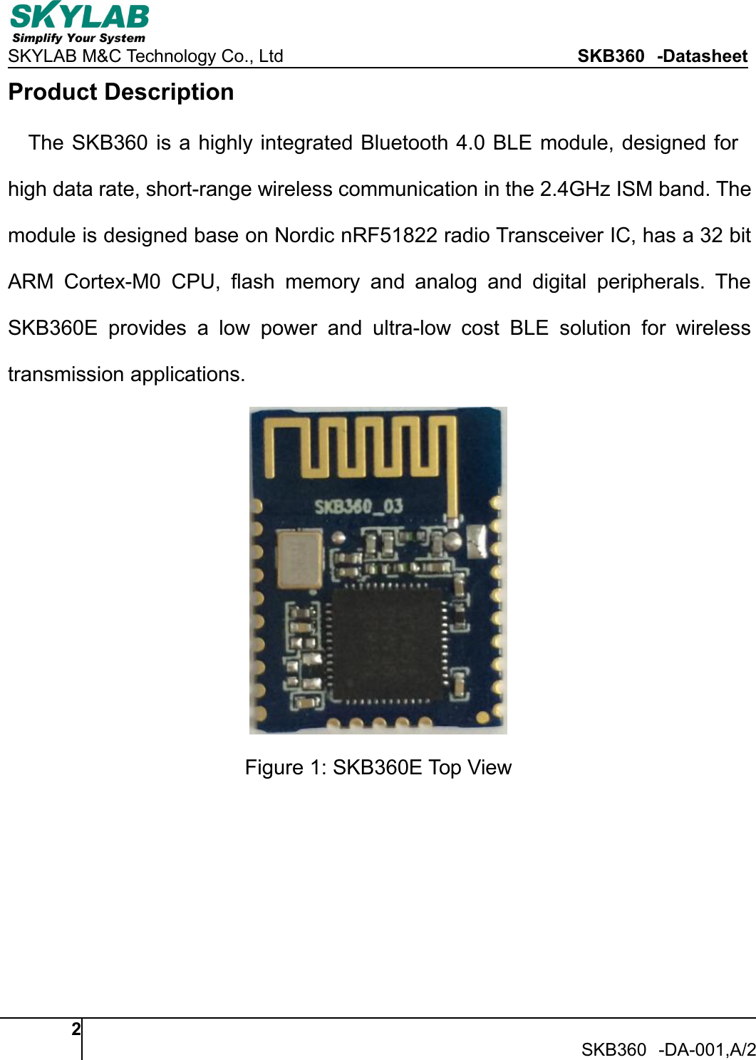
Skylab M and C Technology
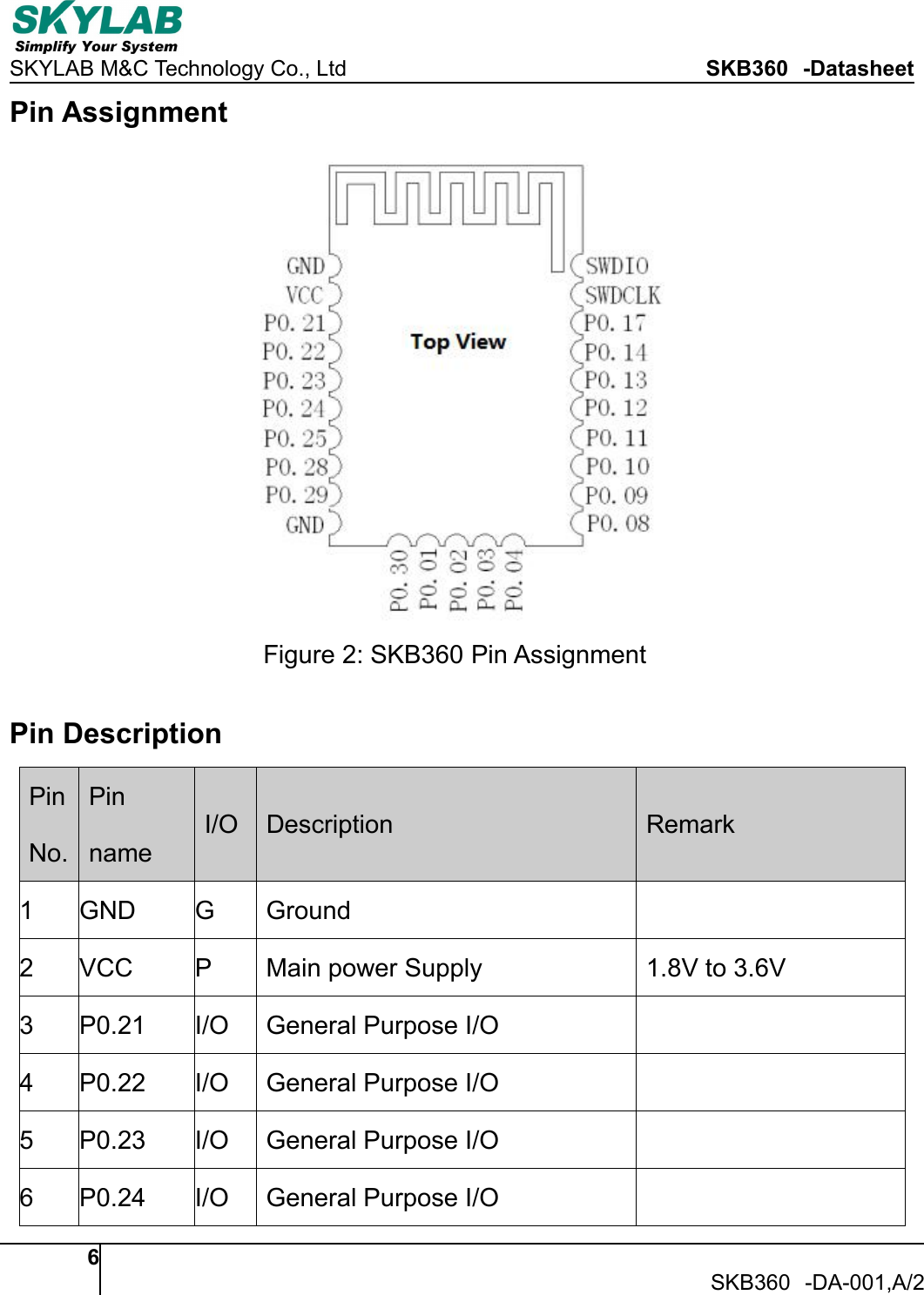
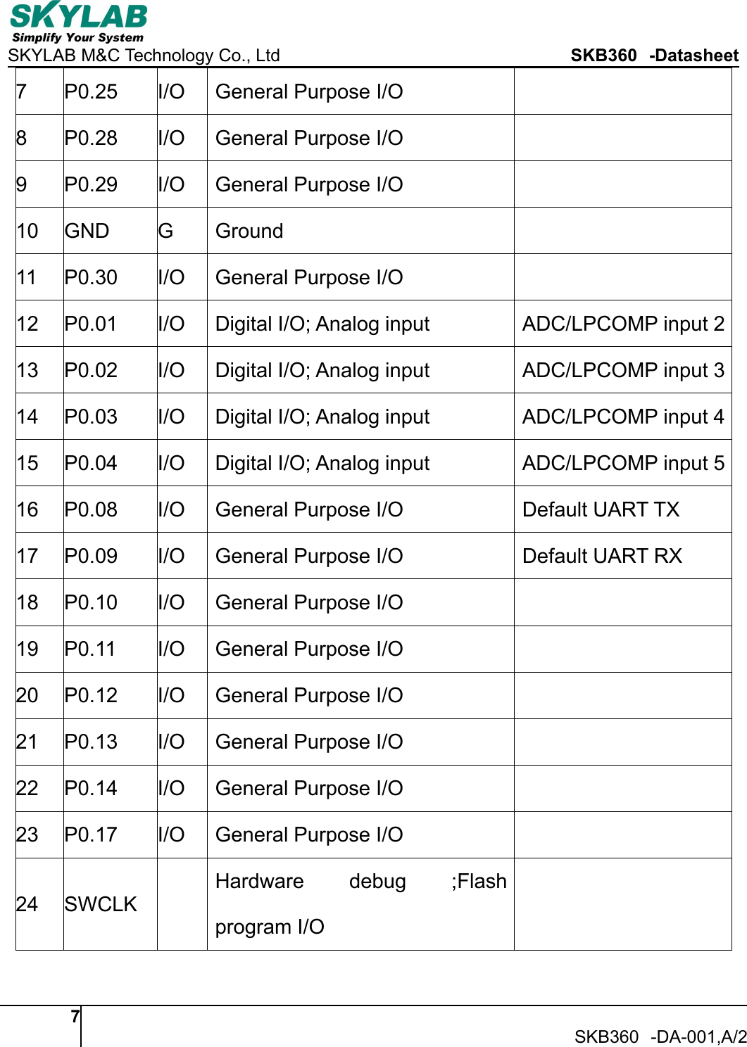
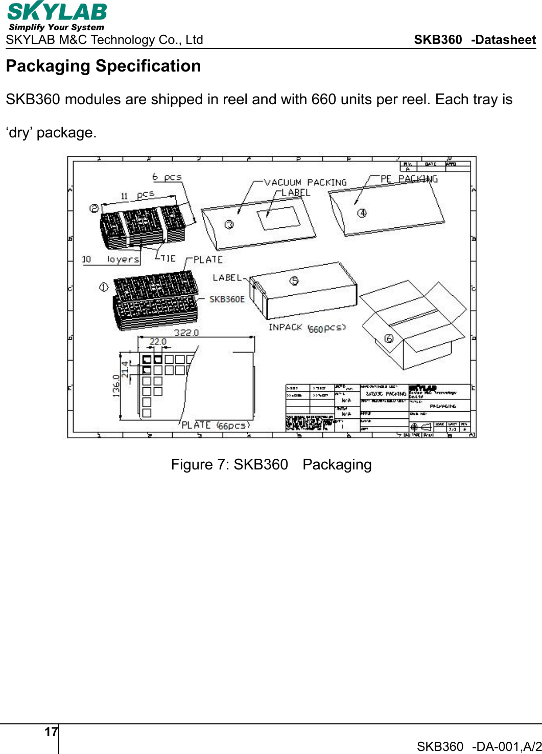
 SKB360 Bluetooth 4.0 Low Energy Module User Manual Ultra High Sensitivity GPS Engine Module

Skylab M&C; Technology Co.,Ltd. Bluetooth 4.0 Low Energy Module Ultra High Sensitivity GPS Engine Module

Users manual

SKYLAB M&C Technology Co., Ltd SKB360 -Datasheet1SKB360 -DA-001,A/2SKB360 Bluetooth 4.0Low Energy ModuleName: Bluetooth 4.0 Low Energy ModuleModel No.: SKB360Version: V2.03Revision History:Revision Description Approved DateV1.01 Initial Release Sunny 20140611V2.01 Upgrade hardware Sunny 20150117V2.02 Added AT instruction Sunny 20150528V2.03 Upgrade hardware Hogan 20160611User Manual
SKYLAB M&C Technology Co., Ltd SKB360 -Datasheet2SKB360 -DA-001,A/2Product DescriptionThe SKB360 is a highly integrated Bluetooth 4.0 BLE module, designed forhigh data rate, short-range wireless communication in the 2.4GHz ISM band. Themodule is designed base on Nordic nRF51822 radio Transceiver IC, has a 32 bitARM Cortex-M0 CPU, flash memory and analog and digital peripherals. TheSKB360E provides a low power and ultra-low cost BLE solution for wirelesstransmission applications.Figure 1: SKB360E Top View
SKYLAB M&C Technology Co., Ltd SKB360 -Datasheet3SKB360 -DA-001,A/2FeaturesMain Chip: nRF51822Bluetooth® 4.0 low energy single-mode protocol stackL2CAP, ATT, GAP,GATT and SM protocolsCentral and Peripheral rolesGATT Client and ServerFull SMP support including MITM and OOB pairing2.4 GHz transceiver-93dBm sensitivity in Bluetooth low energy mode250Kbps, 1Mbps, 2Mbps supported data ratesTx Power -20 to +4 dBm in 4 dB stepsTx Power -30 dBm Whisper modeRSSI (1 dB resolution)Flexible Power ManagementSupply voltage range 1.8V to 3.6V4.2us wake-up using 16MHz RCOSC0.6uA at 3V OFF mode1.2uA at 3V in OFF mode +1 region RAM retention2.6uA at 3V ON mode, all blocks IDLE8/9/10 bit ADC-4 configurable channels
SKYLAB M&C Technology Co., Ltd SKB360 -Datasheet4SKB360 -DA-001,A/220 General Purpose I/O pinsSPI Master/SlaveTwo-wire Master (I2C compatible)UART (CTS/RTS)CPU independent Programmable Peripheral Interconnect (PPI)Quadrature Decoder (QDEC)AES HW encryptionPlate antennaDimension: 17.4x13.7 x1.9 mm
SKYLAB M&C Technology Co., Ltd SKB360 -Datasheet5SKB360 -DA-001,A/2ApplicationsComputer peripherals and I/O devicesMouseKeyboardMulti-touch trackpadInteractive entertainment devicesRemote control3D GlassesGaming controllerPersonal Area NetworksHealth/fitness sensor and monitor devicesMedical devicesKey-fobs + wrist watchesRemote control toys
SKYLAB M&C Technology Co., Ltd SKB360 -Datasheet6SKB360 -DA-001,A/2Pin AssignmentFigure 2: SKB360 Pin AssignmentPin DescriptionPinNo.PinnameI/O Description Remark1 GND G Ground2 VCC P Main power Supply 1.8V to 3.6V3 P0.21 I/O General Purpose I/O4 P0.22 I/O General Purpose I/O5 P0.23 I/O General Purpose I/O6 P0.24 I/O General Purpose I/O
SKYLAB M&C Technology Co., Ltd SKB360 -Datasheet7SKB360 -DA-001,A/27 P0.25 I/O General Purpose I/O8 P0.28 I/O General Purpose I/O9 P0.29 I/O General Purpose I/O10 GND G Ground11 P0.30 I/O General Purpose I/O12 P0.01 I/O Digital I/O; Analog input ADC/LPCOMP input 213 P0.02 I/O Digital I/O; Analog input ADC/LPCOMP input 314 P0.03 I/O Digital I/O; Analog input ADC/LPCOMP input 415 P0.04 I/O Digital I/O; Analog input ADC/LPCOMP input 516 P0.08 I/O General Purpose I/O Default UART TX17 P0.09 I/O General Purpose I/O Default UART RX18 P0.10 I/O General Purpose I/O19 P0.11 I/O General Purpose I/O20 P0.12 I/O General Purpose I/O21 P0.13 I/O General Purpose I/O22 P0.14 I/O General Purpose I/O23 P0.17 I/O General Purpose I/O24 SWCLKHardware debug ;Flashprogram I/O
SKYLAB M&C Technology Co., Ltd SKB360 -Datasheet8SKB360 -DA-001,A/225SWDIO/nRESETHardware debug ;Flashprogram I/O;System reset (active low)Interfaces ConfigurationPower SupplyRegulated power for the SKB360I is required. The input voltage Vcc should be1.8V to 3.6V range, current is no less than 50mA. Suitable decoupling must beprovided by external decoupling circuitry (10uF and 1uF). It can reduce the Noisefrom power supply and increase power stability.Flash program I/OsThe module has two programmer pins, respectively SWCLK pin and SWDIOpin. The two pin Serial Wire Debug (SWD) interface provided as a part of the Debug Access Port (DAP) offers a flexible and powerful mechanism for non-intrusive debugging of program code. Breakpoints and single stepping are part of thissupport.SWDIO can also be use as system reset pin,the system reset pin is avtive low.GPIOThe general purpose I/O is organized as one port with up to 20 I/Os enablingaccess and control of up to 20 pins through one port. Each GPIO can be accessed individually with the following user configurable features:
SKYLAB M&C Technology Co., Ltd SKB360 -Datasheet9SKB360 -DA-001,A/2•Input/output direction•Output drive strength•Internal pull-up and pull-down resistors•Wake-up from high or low level triggers on all pins•Trigger interrupt on all pins•All pins can be used by the PPI task/event system; the maximum number of pins that can be interfaced through the PPI at the same time is limited by the number of GPIOTE channels•All pins can be individually configured to carry serial interface or quadrature demodulator signals•All pins can be configured as PWM signal.There are 4 ADC/LPCOMP input in the 20 I/Os.
SKYLAB M&C Technology Co., Ltd SKB360 -Datasheet10SKB360 -DA-001,A/2Serial Peripheral Interface(SPI/SPIS)The SPI interfaces enable full duplex synchronous communication betweendevices. They support a three-wire (SCK, MISO, MOSI) bi-directional bus withfast data transfers. The SPI Master can communicate with multiple slavesusing individual chip select signals for each of the slave devices attached to abus. Control of chip select signals is left to the application through use of GPIOsignals. SPI Master has double buffered I/O data. The SPI Slave includesEasyDMA for data transfer directly to and from RAM allowing Slave datatransfers to occur while the CPU is IDLE.The SPI peripheral support SPI mode0,1,2,and 3.The module have 3 SPI ports and they properties like followingtable.Instance Master/SlaveSPI0 MasterSPI1 MasterSPIS1 Slave
SKYLAB M&C Technology Co., Ltd SKB360 -Datasheet11SKB360 -DA-001,A/2Two-wire Interface(TWI)The two-wire interface can communicate with a bi-directional wired-AND buswith two lines (SCL, SDA). The protocol makes it possible to interconnect up to127 individually addressable devices. The interface is capable of clockstretching, supporting data rates of 100 kbps and 400 kbps. The module have2 TWI ports and they properties like following table.Instance Master/SlaveTWI0 MasterTWI1 MasterUniversal Asynchronous Receiver/Transmitter (UART)The Universal Asynchronous Receiver/Transmitter offers fast, full-duplex,asynchronous serial communication with built-in flow control (CTS, RTS)support in hardware up to 1 Mbps baud. Parity checking is supported.Notify: The GPIOs used for each SPI/TWI/UART interface line can be chosenfrom any GPIO on the device and are independently configurable.
SKYLAB M&C Technology Co., Ltd SKB360 -Datasheet12SKB360 -DA-001,A/2Operating ConditionsThe operating conditions are the physical parameters that the module canoperate within as defined in tableParameter Symbol Min. Typ. Max. UnitsSupply voltage, normal mode VCC 1.8 3.0 3.6 VSupply rise time (0V to VCC) Tr_vcc 100 msOperating temperature Ta -25 25 75 °CGeneral Purpose I/O(GPIO) specificationsParameter Symbol Min.Typ.Max. UnitsInput high voltage VIH 0.7VDD VDD VInput low voltage VIL VSS 0.3VDD VOutput high voltage VOH VDD-0.3 VDD VOutput low voltage VOL VSS 0.3VDD VPull-up resistance RPU 11 13 16 kΩPull-down resistance PPD 11 13 16 kΩ
SKYLAB M&C Technology Co., Ltd SKB360 -Datasheet13SKB360 -DA-001,A/2Absolute Maximum RatingMaximum ratings are the extreme limits the module can be exposed to withoutcausing permanent damage. Exposure to absolute maximum ratings forprolonged periods of time may affect the reliability of the module.Parameter Symbol Min Max UnitsPower SupplyPower Supply Volt. VCC -0.3 +3.9 VI/0 Pin voltageInput voltage on any inputconnectionVIO -0.3 VCC+0.3 VHuman Body Model ESD HBM 4000 VCharged Device Model ESD CDM 750 VEnvironmentStorage Temperature Tstg -40 +125 °CFlash memory Endurance Write/erase 20000+ timesNumber of times an address canbe written between erase cycles2 times
SKYLAB M&C Technology Co., Ltd SKB360 -Datasheet14SKB360 -DA-001,A/2Reference design schematicFigure 3: SKB360 schematic
SKYLAB M&C Technology Co., Ltd SKB360 -Datasheet15SKB360 -DA-001,A/2Package OutlineFigure 4: SKB360 DimensionsRecommended PCB pad patternFigure 5: SKB360 Layout Package
SKYLAB M&C Technology Co., Ltd SKB360 -Datasheet16SKB360 -DA-001,A/2Manufacturing Process RecommendationsFigure 6: SKB360 Typical Leadfree Soldering ProfileNote :The final soldering temperature chosen at the factory depends onadditional external factors like choice of soldering paste,size,thickness andproperties of the baseboard ,etc. Exceeding the maximum solderingtemperature in the recommended soldering profile may permanently damage themodule.
SKYLAB M&C Technology Co., Ltd SKB360 -Datasheet17SKB360 -DA-001,A/2Packaging SpecificationSKB360 modules are shipped in reel and with 660 units per reel. Each tray is‘dry’ package.Figure 7: SKB360 Packaging
SKYLAB M&C Technology Co., Ltd SKB360 -Datasheet18SKB360 -DA-001,A/2FCC StatementChanges or modifications not expressly approved by the party responsible for compliance could void theuser's authority to operate the equipment.This equipment has been tested and found to comply with the limits for a Class B digital device, pursuant toPart 15 of the FCC Rules. These limits are designed to provide reasonable protection against harmfulinterference in a residential installation. This equipment generates uses and can radiate radio frequencyenergy and, if not installed and used in accordance with theinstructions, may cause harmful interference to radio communications. However, there is no guarantee thatinterference will not occur in a particular installation. If this equipment does cause harmful interference toradio or television reception, which can be determined by turning the equipment off and on, the user isencouraged to try to correct the interference by one or more of the following measures:-- Reorient or relocate the receiving antenna.-- Increase the separation between the equipment and receiver.-- Connect the equipment into an outlet on a circuit different from that to which the receiver is connected.-- Consult the dealer or an experienced radio/TV technician for helpThis device complies with part 15 of the FCC rules. Operation is subject to the following two conditions(1)this device may not cause harmful interference, and (2) this device must accept any interference received,including interference that may cause undesired operation
SKYLAB M&C Technology Co., Ltd SKB360E-Datasheet19SKB360E-DA-001,A/2Skylab M&C Technology Co., Ltd.FCC Radiation Exposure StatementThe modular can be installed or integrated in mobile or fix devices only. This modular cannotbe installed in any portable device, for example, USB dongle like transmitters is forbidden.This modular complies with FCC RF radiation exposure limits set forth for an uncontrolledenvironment. This transmitter must not be collocated or operating in conjunction with any otherantenna or transmitter.If the FCC identification number is not visible when the module is installed inside anotherdevice, then the outside of the device into which the module is installed must also display alabel referring to the enclosed module.This exterior label can use wording such as the following:“Contains Transmitter Module FCC ID:2ACOE-SKB360 Or Contains FCC ID:2ACOE-SKB360''when the module is installed inside another device, the user manual of this device mustcontain below warning statements;1. This device complies with Part 15 of the FCC Rules. Operation is subject to the followingtwo conditions:(1) This device may not cause harmful interference.(2) This device must accept any interference received, including interference that may causeundesired operation.2. Changes or modifications not expressly approved by the party responsible for compliancecould void the user's authority to operate the equipment.The devices must be installed and used in strict accordance with the manufacturer'sinstructions as described in the user documentation that comes with the product.

Navigation menu