Skylab M and C Technology SKB360 Bluetooth 4.0 Low Energy Module User Manual Ultra High Sensitivity GPS Engine Module
Skylab M&C; Technology Co.,Ltd. Bluetooth 4.0 Low Energy Module Ultra High Sensitivity GPS Engine Module
Users manual

SKYLAB M&C Technology Co., Ltd SKB360 -Datasheet
1
SKB360 -DA-001,A/2
SKB360 Bluetooth 4.0
Low Energy Module
Name: Bluetooth 4.0 Low Energy Module
Model No.: SKB360
Version: V2.03
Revision History:
Revision Description Approved Date
V1.01 Initial Release Sunny 20140611
V2.01 Upgrade hardware Sunny 20150117
V2.02 Added AT instruction Sunny 20150528
V2.03 U
pg
rade hardware Ho
g
an 20160611
User Manual
SKYLAB M&C Technology Co., Ltd SKB360 -Datasheet
2
SKB360 -DA-001,A/2
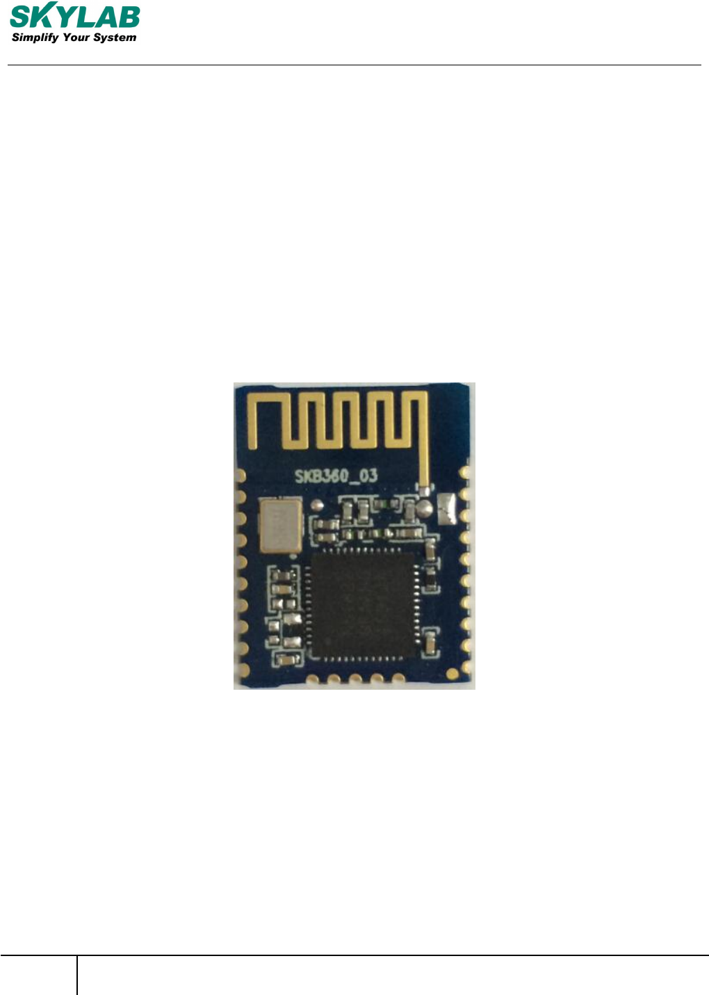
Product Description
The SKB360 is a highly integrated Bluetooth 4.0 BLE module, designed for
high data rate, short-range wireless communication in the 2.4GHz ISM band. The
module is designed base on Nordic nRF51822 radio Transceiver IC, has a 32 bit
ARM Cortex-M0 CPU, flash memory and analog and digital peripherals. The
SKB360E provides a low power and ultra-low cost BLE solution for wireless
transmission applications.
Figure 1: SKB360E Top View

SKYLAB M&C Technology Co., Ltd SKB360 -Datasheet
3
SKB360 -DA-001,A/2
Features
Main Chip: nRF51822
Bluetooth® 4.0 low energy single-mode protocol stack
L2CAP, ATT, GAP,GATT and SM protocols
Central and Peripheral roles
GATT Client and Server
Full SMP support including MITM and OOB pairing
2.4 GHz transceiver
-93dBm sensitivity in Bluetooth low energy mode
250Kbps, 1Mbps, 2Mbps supported data rates
Tx Power -20 to +4 dBm in 4 dB steps
Tx Power -30 dBm Whisper mode
RSSI (1 dB resolution)
Flexible Power Management
Supply voltage range 1.8V to 3.6V
4.2us wake-up using 16MHz RCOSC
0.6uA at 3V OFF mode
1.2uA at 3V in OFF mode +1 region RAM retention
2.6uA at 3V ON mode, all blocks IDLE
8/9/10 bit ADC-4 configurable channels

SKYLAB M&C Technology Co., Ltd SKB360 -Datasheet
4
SKB360 -DA-001,A/2
20 General Purpose I/O pins
SPI Master/Slave
Two-wire Master (I2C compatible)
UART (CTS/RTS)
CPU independent Programmable Peripheral Interconnect (PPI)
Quadrature Decoder (QDEC)
AES HW encryption
Plate antenna
Dimension: 17.4x13.7 x1.9 mm

SKYLAB M&C Technology Co., Ltd SKB360 -Datasheet
5
SKB360 -DA-001,A/2
Applications
Computer peripherals and I/O devices
Mouse
Keyboard
Multi-touch trackpad
Interactive entertainment devices
Remote control
3D Glasses
Gaming controller
Personal Area Networks
Health/fitness sensor and monitor devices
Medical devices
Key-fobs + wrist watches
Remote control toys
SKYLAB M&C Technology Co., Ltd SKB360 -Datasheet
6
SKB360 -DA-001,A/2
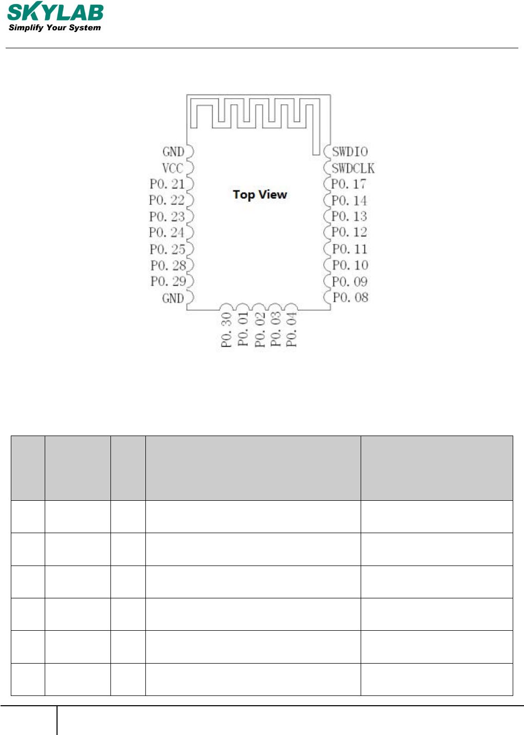
Pin Assignment
Figure 2: SKB360 Pin Assignment
Pin Description
Pin
No.
Pin
name
I/O Description Remark
1 GND G Ground
2 VCC P Main power Supply 1.8V to 3.6V
3 P0.21 I/O General Purpose I/O
4 P0.22 I/O General Purpose I/O
5 P0.23 I/O General Purpose I/O
6 P0.24 I/O General Purpose I/O

SKYLAB M&C Technology Co., Ltd SKB360 -Datasheet
7
SKB360 -DA-001,A/2
7 P0.25 I/O General Purpose I/O
8 P0.28 I/O General Purpose I/O
9 P0.29 I/O General Purpose I/O
10 GND G Ground
11 P0.30 I/O General Purpose I/O
12 P0.01 I/O Digital I/O; Analog input ADC/LPCOMP input 2
13 P0.02 I/O Digital I/O; Analog input ADC/LPCOMP input 3
14 P0.03 I/O Digital I/O; Analog input ADC/LPCOMP input 4
15 P0.04 I/O Digital I/O; Analog input ADC/LPCOMP input 5
16 P0.08 I/O General Purpose I/O Default UART TX
17 P0.09 I/O General Purpose I/O Default UART RX
18 P0.10 I/O General Purpose I/O
19 P0.11 I/O General Purpose I/O
20 P0.12 I/O General Purpose I/O
21 P0.13 I/O General Purpose I/O
22 P0.14 I/O General Purpose I/O
23 P0.17 I/O General Purpose I/O
24 SWCLK
Hardware debug ;Flash
program I/O

SKYLAB M&C Technology Co., Ltd SKB360 -Datasheet
8
SKB360 -DA-001,A/2
25
SWDIO/
nRESET
Hardware debug ;Flash
program I/O;
System reset (active low)
Interfaces Configuration
Power Supply
Regulated power for the SKB360I is required. The input voltage Vcc should be
1.8V to 3.6V range, current is no less than 50mA. Suitable decoupling must be
provided by external decoupling circuitry (10uF and 1uF). It can reduce the Noise
from power supply and increase power stability.
Flash program I/Os
The module has two programmer pins, respectively SWCLK pin and SWDIO
pin. The two pin Serial Wire Debug (SWD) interface provided as a part of the De
bug Access Port (DAP) offers a flexible and powerful mechanism for non-intrusiv
e debugging of program code. Breakpoints and single stepping are part of this
support.
SWDIO can also be use as system reset pin,the system reset pin is avtive low.
GPIO
The general purpose I/O is organized as one port with up to 20 I/Os enabling
access and control of up to 20 pins through one port. Each GPIO can be access
ed individually with the following user configurable features:

SKYLAB M&C Technology Co., Ltd SKB360 -Datasheet
9
SKB360 -DA-001,A/2
•Input/output direction
•Output drive strength
•Internal pull-up and pull-down resistors
•Wake-up from high or low level triggers on all pins
•Trigger interrupt on all pins
•All pins can be used by the PPI task/event system; the maximum number of pin
s that can be interfaced through the PPI at the same time is limited by the numb
er of GPIOTE channels
•All pins can be individually configured to carry serial interface or quadrature de
modulator signals
•All pins can be configured as PWM signal.
There are 4 ADC/LPCOMP input in the 20 I/Os.
SKYLAB M&C Technology Co., Ltd SKB360 -Datasheet
10
SKB360 -DA-001,A/2
Serial Peripheral Interface(SPI/SPIS)
The SPI interfaces enable full duplex synchronous communication between
devices. They support a three-wire (SCK, MISO, MOSI) bi-directional bus with
fast data transfers. The SPI Master can communicate with multiple slaves
using individual chip select signals for each of the slave devices attached to a
bus. Control of chip select signals is left to the application through use of GPIO
signals. SPI Master has double buffered I/O data. The SPI Slave includes
EasyDMA for data transfer directly to and from RAM allowing Slave data
transfers to occur while the CPU is IDLE.The SPI peripheral support SPI mode
0,1,2,and 3.The module have 3 SPI ports and they properties like following
table.
Instance Master/Slave
SPI0 Master
SPI1 Master
SPIS1 Slave
SKYLAB M&C Technology Co., Ltd SKB360 -Datasheet
11
SKB360 -DA-001,A/2
Two-wire Interface(TWI)
The two-wire interface can communicate with a bi-directional wired-AND bus
with two lines (SCL, SDA). The protocol makes it possible to interconnect up to
127 individually addressable devices. The interface is capable of clock
stretching, supporting data rates of 100 kbps and 400 kbps. The module have
2 TWI ports and they properties like following table.
Instance Master/Slave
TWI0 Master
TWI1 Master
Universal Asynchronous Receiver/Transmitter (UART)
The Universal Asynchronous Receiver/Transmitter offers fast, full-duplex,
asynchronous serial communication with built-in flow control (CTS, RTS)
support in hardware up to 1 Mbps baud. Parity checking is supported.
Notify: The GPIOs used for each SPI/TWI/UART interface line can be chosen
from any GPIO on the device and are independently configurable.
SKYLAB M&C Technology Co., Ltd SKB360 -Datasheet
12
SKB360 -DA-001,A/2
Operating Conditions
The operating conditions are the physical parameters that the module can
operate within as defined in table
Parameter Symbol Min. Typ. Max. Units
Supply voltage, normal mode VCC 1.8 3.0 3.6 V
Supply rise time (0V to VCC) Tr_vcc 100 ms
Operating temperature Ta -25 25 75 °C
General Purpose I/O(GPIO) specifications
Parameter Symbol Min.
Typ
.Max. Units
Input high voltage VIH 0.7VDD VDD V
Input low voltage VIL VSS 0.3VDD V
Output high voltage VOH VDD-0.3 VDD V
Output low voltage VOL VSS 0.3VDD V
Pull-up resistance RPU 11 13 16 kΩ
Pull-down resistance PPD 11 13 16 kΩ
SKYLAB M&C Technology Co., Ltd SKB360 -Datasheet
13
SKB360 -DA-001,A/2
Absolute Maximum Rating
Maximum ratings are the extreme limits the module can be exposed to without
causing permanent damage. Exposure to absolute maximum ratings for
prolonged periods of time may affect the reliability of the module.
Parameter Symbol Min Max Units
Power Supply
Power Supply Volt. VCC -0.3 +3.9 V
I/0 Pin voltage
Input voltage on any input
connection
VIO -0.3 VCC+0.3 V
Human Body Model ESD HBM 4000 V
Charged Device Model ESD CDM 750 V
Environment
Storage Temperature Tstg -40 +125 °C
Flash memory Endurance Write/erase 20000+ times
Number of times an address can
be written between erase cycles
2 times
SKYLAB M&C Technology Co., Ltd SKB360 -Datasheet
14
SKB360 -DA-001,A/2
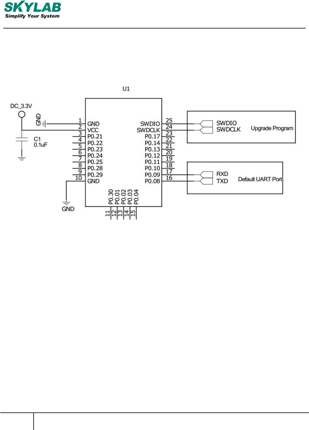
Reference design schematic
Figure 3: SKB360 schematic
SKYLAB M&C Technology Co., Ltd SKB360 -Datasheet
15
SKB360 -DA-001,A/2
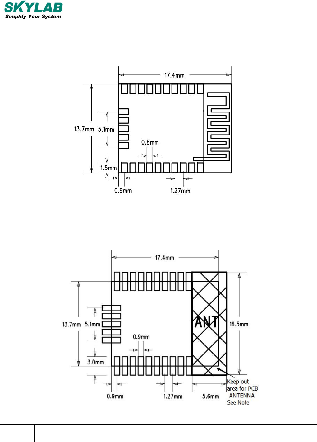
Package Outline
Figure 4: SKB360 Dimensions
Recommended PCB pad pattern
Figure 5: SKB360 Layout Package

SKYLAB M&C Technology Co., Ltd SKB360 -Datasheet
16
SKB360 -DA-001,A/2
Manufacturing Process Recommendations
Figure 6: SKB360 Typical Leadfree Soldering Profile
Note :The final soldering temperature chosen at the factory depends on
additional external factors like choice of soldering paste,size,thickness and
properties of the baseboard ,etc. Exceeding the maximum soldering
temperature in the recommended soldering profile may permanently damage the
module.
SKYLAB M&C Technology Co., Ltd SKB360 -Datasheet
17
SKB360 -DA-001,A/2
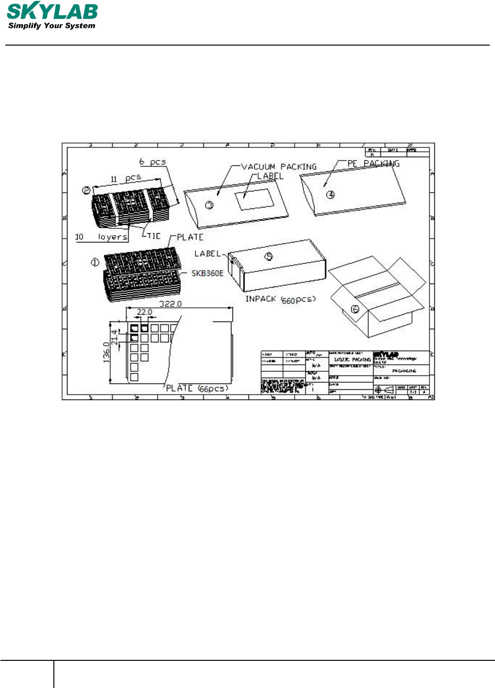
Packaging Specification
SKB360 modules are shipped in reel and with 660 units per reel. Each tray is
‘dry’ package.
Figure 7: SKB360 Packaging

SKYLAB M&C Technology Co., Ltd SKB360 -Datasheet
18
SKB360 -DA-001,A/2
FCC Statement
Changes or modifications not expressly approved by the party responsible for compliance could void the
user's authority to operate the equipment.
This equipment has been tested and found to comply with the limits for a Class B digital device, pursuant to
Part 15 of the FCC Rules. These limits are designed to provide reasonable protection against harmful
interference in a residential installation. This equipment generates uses and can radiate radio frequency
energy and, if not installed and used in accordance with the
instructions, may cause harmful interference to radio communications. However, there is no guarantee that
interference will not occur in a particular installation. If this equipment does cause harmful interference to
radio or television reception, which can be determined by turning the equipment off and on, the user is
encouraged to try to correct the interference by one or more of the following measures:
-- Reorient or relocate the receiving antenna.
-- Increase the separation between the equipment and receiver.
-- Connect the equipment into an outlet on a circuit different from that to which the receiver is connected.
-- Consult the dealer or an experienced radio/TV technician for help
This device complies with part 15 of the FCC rules. Operation is subject to the following two conditions
(1)this device may not cause harmful interference, and (2) this device must accept any interference received,
including interference that may cause undesired operation

SKYLAB M&C Technology Co., Ltd SKB360E-Datasheet
19
SKB360E-DA-001,A/2
Skylab M&C Technology Co., Ltd.
FCC Radiation Exposure Statement
The modular can be installed or integrated in mobile or fix devices only. This modular cannot
be installed in any portable device, for example, USB dongle like transmitters is forbidden.
This modular complies with FCC RF radiation exposure limits set forth for an uncontrolled
environment. This transmitter must not be collocated or operating in conjunction with any other
antenna or transmitter.
If the FCC identification number is not visible when the module is installed inside another
device, then the outside of the device into which the module is installed must also display a
label referring to the enclosed module.
This exterior label can use wording such as the following:
“Contains Transmitter Module FCC ID:2ACOE-SKB360 Or Contains FCC ID:2ACOE-SKB360''
when the module is installed inside another device, the user manual of this device must
contain below warning statements;
1. This device complies with Part 15 of the FCC Rules. Operation is subject to the following
two conditions:
(1) This device may not cause harmful interference.
(2) This device must accept any interference received, including interference that may cause
undesired operation.
2. Changes or modifications not expressly approved by the party responsible for compliance
could void the user's authority to operate the equipment.
The devices must be installed and used in strict accordance with the manufacturer's
instructions as described in the user documentation that comes with the product.