Sony Group CPWL0102U 802.11bgn WLAN Module User Manual B010 datasheet V03 201008023 Sony
Sony Corporation 802.11bgn WLAN Module B010 datasheet V03 201008023 Sony
User Manual

CWPL Series
第 1 頁,共 15 頁
CWPL
series
Hardware
Specification
Rev. 0.3
CWPL Series
第 2 頁,共 15 頁
Document Revision History
Document
Revision Date Modifier Comments
0.1 Apr. 19, 2010
Yishin Wu Initial release
0.2 Aug. 13, 2010
Yishin Wu
Add Power consumption, Tx power
Spec, Rx Sensitivity, Module perspective,
Mechanical drawing, Label drawing,
0.3 Aug. 23, 2010
Yishin Wu Update Label content, Ragulatory

CWPL Series
第 3 頁,共 15 頁
Contents
1. INTRODUCTION ...................................................................................... 6
1.1 Product Overview ......................................................................................... 6
1.2 Key Features ................................................................................................. 6
3. ELECTRICAL SPECIFICATIONS ............................................................ 7
3.1 Pin Definitions .............................................................................................. 7
3.2 DC Specifications ......................................................................................... 8
3.2.1 Power Consumption Specifications......................................................... 8
4.
RF SPECIFICATION .............................................................................. 9
4.1 TX Specifications .......................................................................................... 9
4.2 RX Specifications ....................................................................................... 10
4.3 Antenna Specifications .............................................................................. 11
5. MECHANICAL SPECIFICATIONS ........................................................ 12
5.1 Mechanical Drawing ................................................................................... 12
5.2 RF connector .............................................................................................. 13
5.2.1 Specification ............................................................................................ 13
5.2.2 Dimensions: (Unit: mm) .......................................................................... 13
5.3 Label Specifications ................................................................................... 13
6. ENVIRONMENTAL SPECIFICATIONS ................................................. 14

CWPL Series
第 4 頁,共 15 頁
7. PART NUMBERING ............................................................................... 14
7.1 Part Numbering ........................................................................................... 14
7.2 ID Definitions .............................................................................................. 15
8. REGULATORY ....................................................................................... 15

CWPL Series
第 5 頁,共 15 頁
Figures
Figure 2.2 CWPL010 Series block diagram .................................................... 7
Figure 4.1 Two Connector- CWPL010 series perspective ............................. 11
Figure 5.1 Two Connector- CWPL010 series mechanical drawing .............. 12
Figure 5.2 RF connector Dimensions ............................................................. 13
Figure 5.3 CWPL0102U Label drawing ........................................................... 13
Figure 7.1 Part Numbering ............................................................................... 14
Tables
Table 3.1 Pin Definitions .................................................................................... 7
Table 3.2 DC Specifications ............................................................................... 8
Table 3.3 Power Consumption Specifications ................................................. 8
Table 4.1 TX Specifications ............................................................................... 9
Table 4.2 RX Specifications ............................................................................. 10
Table 6.1 Operating Conditions ....................................................................... 14
Table 6.2 Non-operating Conditions ............................................................... 14
Table 7.1 ID Definitions .................................................................................... 15

CWPL Series
第 6 頁,共 15 頁
1. Introduction
1.1 Product Overview
The Sony CWPL010 series wireless LAN module contains the Ralink® RT3370 single
chip which is a highly integrated MAC/BBP for 2.4GHz RF transmission and supporting
150Mbps PHY rate. It fully complies with IEEE 802.11 b/g/n feature rich wireless
connectivity at high standards, delivers reliable, cost-effective, throughput from an extended
distance. The optimized radio frequency architecture and baseband algorithms provide super
performance and low power consumption. Deploy a high efficient USB engine and hardware
data processing accelerators without overloading the host processor. Security, quality of
service and international regulation are supported by CWPL010 series and giving end users
the greatest performance anytime in any circumstance.
1.2 Key Features
Legacy data rates 1, 2 in DSSS mode and rates 5.5, and 11 Mbps in CCK
mode, 6, 9, 12, 18, 24, 36, 48, and 54 in OFDM mode
Support 40MHz wide channel bandwidth
Uses the 2.412 to 2.497GHz ISM frequency band defined by the IEEE
802.11b/g/n specifications
Reverse direction grant data flow and frame aggregation
WEP 64/128, WPA, WPA2, TKIP, AES
QoS-WMM, WMM-PS, WPS, PIN, PBC
Multiple BSSID Support
Form Factor: PCI Express 1.1 Half Mini Card(single side)
International Regulation – 802.11d + h
Cisco CCX Support up to v5.0
Operating Systems – Windows XP 32/64, 2000, Vista 32/64, Linux, Macintosh,Win7
32/64
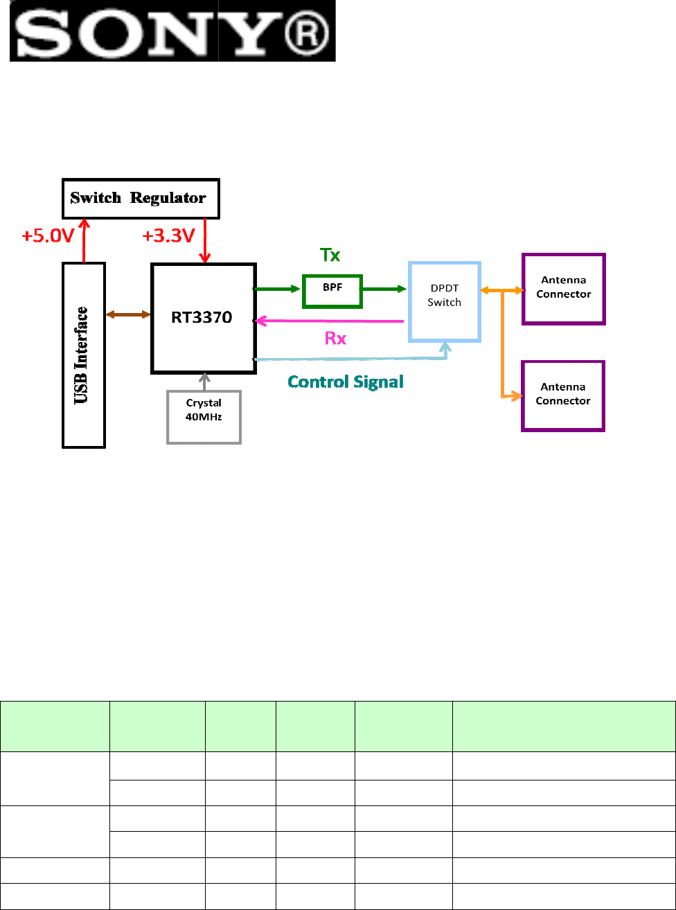
2. System Architecture
Figure 2.1
3.
Electrical Specifications
3.1 Pin Definitions
Signal
Group Signal
USB Interface D+
D-
Power +5.0V +5.0V
GND
WSP WSP
GND GND
第 7 頁,共 15 頁
2. System Architecture
Figure 2.1
CWPL010 Series block diagram
Electrical Specifications
Table 3.1 Pin Definitions
Name Pin No. Direction
UDP 2 Input/Output
differential pair
UDM 3 Input/Output
differential pair
UV+ 4 Input +5.0
V source
GND 1 N/A
Return current path
WSP 6 Input/Output
GND 5 N/A
Return current path
CWPL Series
Description
differential pair
for transmit
differential pair
for receive
V source
Return current path
Return current path
CWPL Series
第 8 頁,共 15 頁
3.2 DC Specifications
The Max Power (as max defined in USB Spec) is 2500mW 500mA
For all USB voltage rails (5.0V), it is recommended not to exceed 100mVpp noise in the
frequency range of 10-500KHz.
Table 3.2 DC Specifications
Parameters Symbol Conditions Min.
Typ.
Max.
Unit
5V Supply Voltage +UV - 4.75
5.0 5.25
V
3.2.1 Power Consumption Specifications
Power consumption is measured using current probe loop on the Power rails of the USB
interface (Pins). Assuming ASMP enabled (L1-active enabled and L0s is disabled).
Table 3.3 Power Consumption Specifications
Test Mode Description
Idle Power Consumption of idle. Assuming average power consumption is in
room temperature.
Average Power: 575 mW
1 Stream
Transmitting and
Receiving
Power Consumption of Transmit and Receive state, assuming Single spatial
stream transmission for 802.11b network
Average Power: 1085 mW
1 Stream
Transmitting and
Receiving
Power Consumption of Transmit and Receive state, assuming Single spatial
stream transmission for 802.11g network
Average Power: 930 mW
1 Stream
Transmitting and
Receiving
Power Consumption of Transmit and Receive state, assuming Single spatial
stream transmission for 802.11n (HT20) network
Average Power: 985 mW
1 Stream
Transmitting and
Receiving
Power Consumption of Transmit and Receive state, assuming Single spatial
stream transmission for 802.11n (HT40) network
Average Power: 975 mW
CWPL Series
第 9 頁,共 15 頁
4. RF Specification
4.1 TX Specifications
Table 4.1 TX Specifications
ModData
Rate
(Mbps)
Modulation
Tx Target Power
(dBm)
Data Rate
(Mbps) Modulation Tx Target Power
(dBm)
1 DBPSK 15 HT20-7.22 BPSK 15
2 DQPSK 15 HT20-14.44 QPSK 15
5.5 CCK 15 HT20-21.67 QPSK 15
11 CCK 15 HT20-28.89 16-QAM 15
6 OFDM 15 HT20-43.33 16-QAM 15
9 OFDM 15 HT20-57.78 64-QAM 15
12 OFDM 15 HT20-65 64-QAM 14
18 OFDM 15 HT20-72.22 64-QAM 14
24 OFDM 15 HT40-15 BPSK 15
36 OFDM 15 HT40-30 QPSK 15
48 OFDM 15 HT40-45 QPSK 15
54 OFDM 15 HT40-60 16-QAM 15
HT40-90 16-QAM 15
HT40-120 64-QAM 15
HT40-135 64-QAM 14
HT40-150 64-QAM 14
※Each tolerance is ±1.5dBm
CWPL Series
第 10 頁,共 15 頁
4.2 RX Specifications
Table 4.2 RX Specifications
Data Rate
(Mbps) Modulation
Rx Sensitivity
(dBm)
Data Rate
(Mbps) Modulation Rx Sensitivity
(dBm)
1 DBPSK -92 HT20-7.22 BPSK -87
2 DQPSK -91 HT20-14.44 QPSK -83
5.5 CCK -91 HT20-21.67 QPSK -82
11 CCK -88 HT20-28.89 16-QAM -79
6 OFDM -88 HT20-43.33 16-QAM -76
9 OFDM -87 HT20-57.78 64-QAM -72
12 OFDM -85 HT20-65 64-QAM -70
18 OFDM -83 HT20-72.22 64-QAM -67
24 OFDM -81 HT40-15 BPSK -85
36 OFDM -77 HT40-30 QPSK -81
48 OFDM -73 HT40-45 QPSK -79
54 OFDM -70 HT40-60 16-QAM -77
HT40-90 16-QAM -73
HT40-120 64-QAM -69
HT40-135 64-QAM -67
HT40-150 64-QAM -65
CWPL Series
第 11 頁,共 15 頁
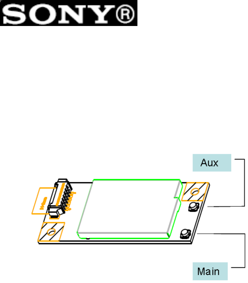
4.3 Antenna Specifications
Nominal antenna port impedance specification is 50 ohms for the Sony CWPL010 series
hardware.
For regulatory requirements, it is assumed that the antenna gain is:
Antenna gain for the 2.4GHz band : 1.6dBi
There are two antennas supporting 2.4-2.5GHz band.
The Sony HD96017 connector will be used on the Sony CWPL010 series hardware.
The antenna will be defined Main and Aux where is listing below:
Figure 4.1 Two Connector- CWPL010 series Perspective
CWPL Series
第 12 頁,共 15 頁
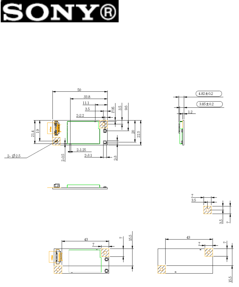
5. Mechanical Specifications
5.1 Mechanical Drawing
Figure 5.1 Two Connector- CWPL010 series mechanical drawing
CWPL Series
第 13 頁,共 15 頁
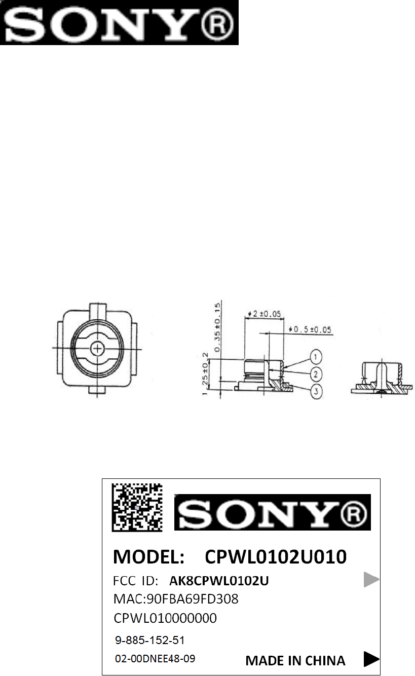
5.2 RF connector
Manufacturer: Sony
Manufacturer P/N: HD96017
5.2.1 Specification
Operating temperature range: -40℃
℃℃
℃~90℃
℃℃
℃
Storage temperature range: -40℃
℃℃
℃~90℃
℃℃
℃
Characteristic impedance: 50Ω (0~3GHz)
Voltage standing wave ratio: VSWR<=1.3 (0.045~3GHz)
5.2.2 Dimensions: (Unit: mm)
Figure 5.2 RF connector dimensions
5.3 Label Specifications
Figure 5.3 CWPL0102U Label Drawing
CWPL Series
第 14 頁,共 15 頁
6. Environmental Specifications
The following tables provide normal operating conditions and maximum rating requirements
for CWPL010 series hardware.
Table 6.1 Operating Conditions
Environment
Limits
Operating 0-70℃
※The radio parts at operating state and above temperature of T-shield.
Table 6.2 Non-operating Conditions
Environment Temperature Humidity
Min.
Typ.
Max.
Unit
Min.
Typ.
Max.
Unit
Non-Operating
-25
25 65 ℃ 45 - 90 %
※ Temperature condition for storage (Packaged) in warehouse is Maximum 40℃ up to 6 months.
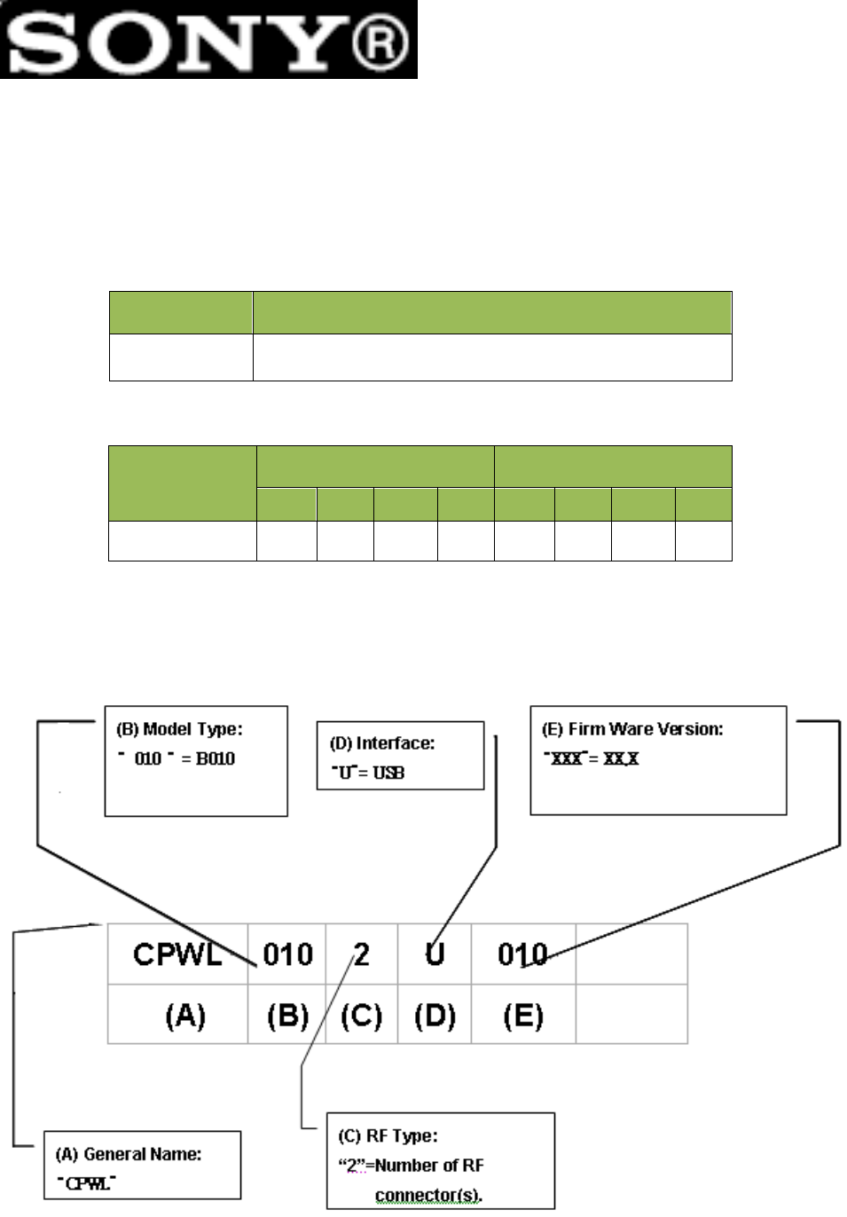
7. Part Numbering
7.1 Part Numbering
Figure 7.1 Part Numbering
CWPL Series
第 15 頁,共 15 頁
7.2 ID Definitions
Table 7.1 ID Definitions
WLAN Type Mode PID VID
CPWL101UXXX-RT3370
BGN 0x0006 0x0489
8. Regulatory
Channel Setting
Active
Passive
Disable
FCC
Ch1-Ch11
Ch12-Ch13
Ch14
Federal Communication Commission Interference Statement
This equipment has been tested and found to comply with the limits for a Class B digital device, pursuant to
Part 15 of the FCC Rules. These limits are designed to provide reasonable protection against harmful
interference in a residential installation. This equipment generates, uses and can radiate radio frequency
energy and, if not installed and used in accordance with the instructions, may cause harmful interference to
radio communications. However, there is no guarantee that interference will not occur in a particular
installation. If this equipment does cause harmful interference to radio or television reception, which can be
determined by turning the equipment off and on, the user is encouraged to try to correct the interference by
one of the following measures:
- Reorient or relocate the receiving antenna.
- Increase the separation between the equipment and receiver.
- Connect the equipment into an outlet on a circuit different from that to which the receiver is connected.
- Consult the dealer or an experienced radio/TV technician for help.
This device complies with Part 15 of the FCC Rules. Operation is subject to the following two conditions: (1)
This device may not cause harmful interference, and (2) this device must accept any interference received,
including interference that may cause undesired operation.
FCC Caution: Any changes or modifications not expressly approved by the party responsible for
compliance could void the user's authority to operate this equipment.
IMPORTANT NOTE:
FCC Radiation Exposure Statement:
This equipment complies with FCC radiation exposure limits set forth for an uncontrolled environment. This
equipment should be installed and operated with minimum distance 20cm between the radiator & your body.
This transmitter must not be co-located or operating in conjunction with any other antenna or transmitter.
IEEE 802.11b or 802.11g operation of this product in the U.S.A. is firmware-limited to channels 1 through 11.
This device is intended only for OEM integrators under the following conditions:
1) The antenna must be installed such that 20 cm is maintained between the antenna and users,
and
2) The transmitter module may not be co-located with any other transmitter or antenna,
3) For all products market in US, OEM has to limit the operation channels in CH1 to CH11 for 2.4G
band by supplied firmware programming tool. OEM shall not supply any tool or info to the end-user
regarding to Regulatory Domain change.
As long as 3 conditions above are met, further transmitter test will not be required. However, the OEM
integrator is still responsible for testing their end-product for any additional compliance requirements
required with this module installed (for example, digital device emissions, PC peripheral requirement, etc.).

IMPORTANT NOTE: In the event that these conditions can not be met (for example certain laptop
configurations or co-location with another transmitter), then the FCC authorization is no longer considered
valid and the FCC ID can not be used on the final product. In these circumstances, the OEM integrator will
be responsible for re-evaluating the end product (including the transmitter) and obtaining a separate FCC
authorization.
End Product Labeling
This transmitter module is authorized only for use in device where the antenna may be installed
such that 20 cm may be maintained between the antenna and users. The final end product must
be labeled in a visible area with the following: “Contains FCC ID:AK8CPWL0102U”.
Manual Information To the End User
The OEM integrator has to be aware not to provide information to the end user regarding how to install or
remove this RF module in the user's manual of the end product which integrates this module.
The end user manual shall include all required regulatory information/warning as show in this manual.