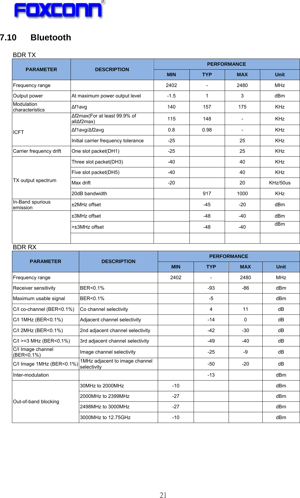
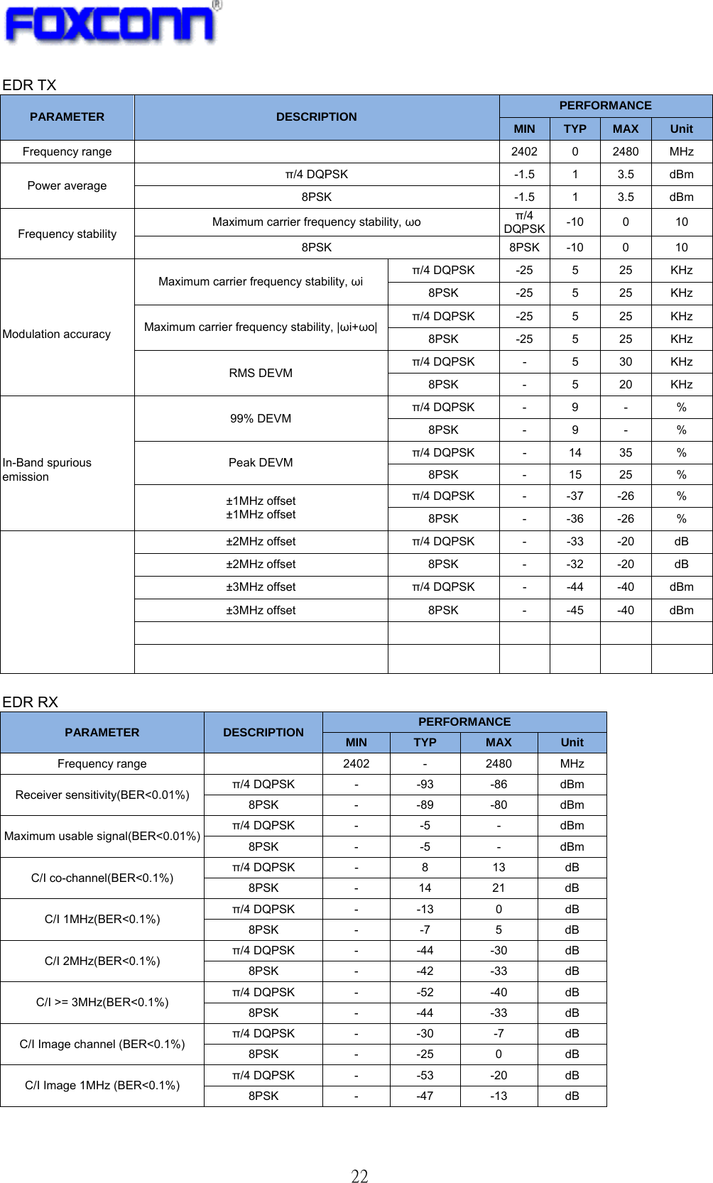
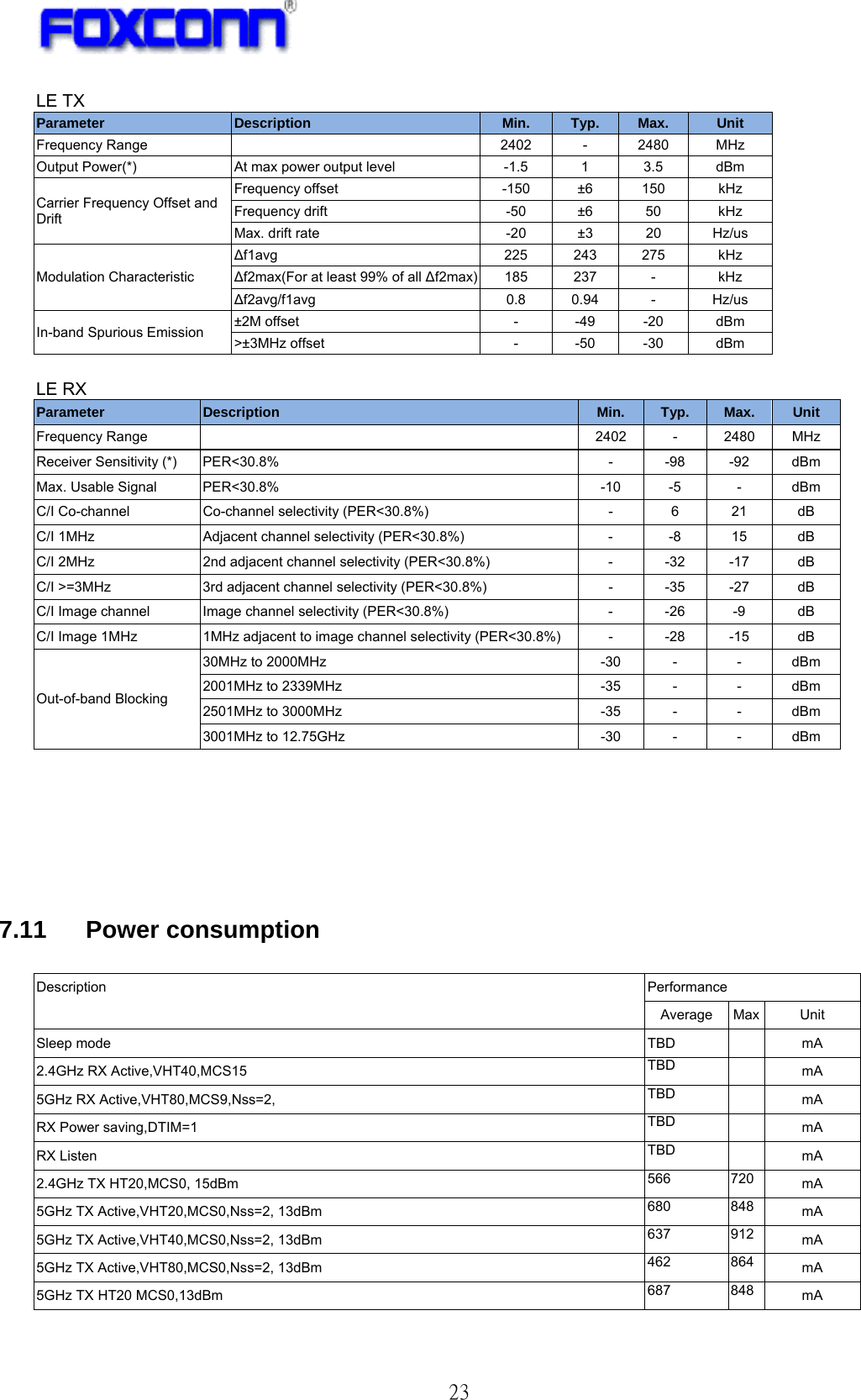
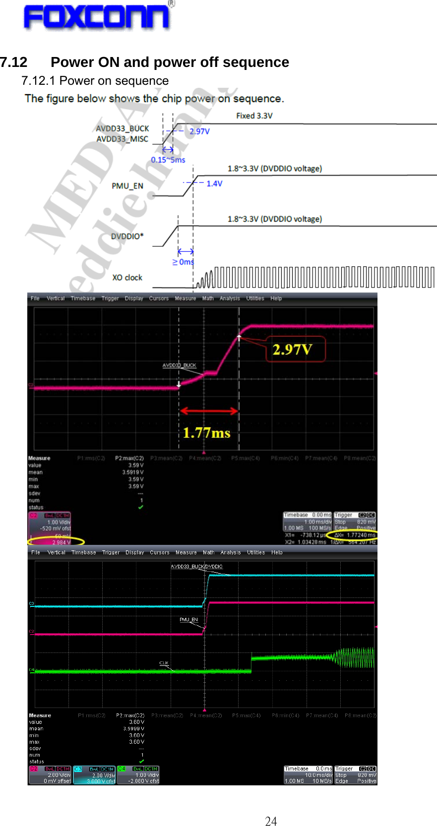
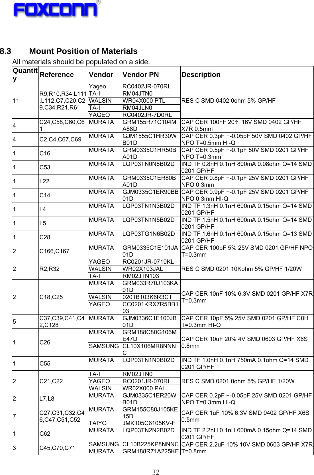
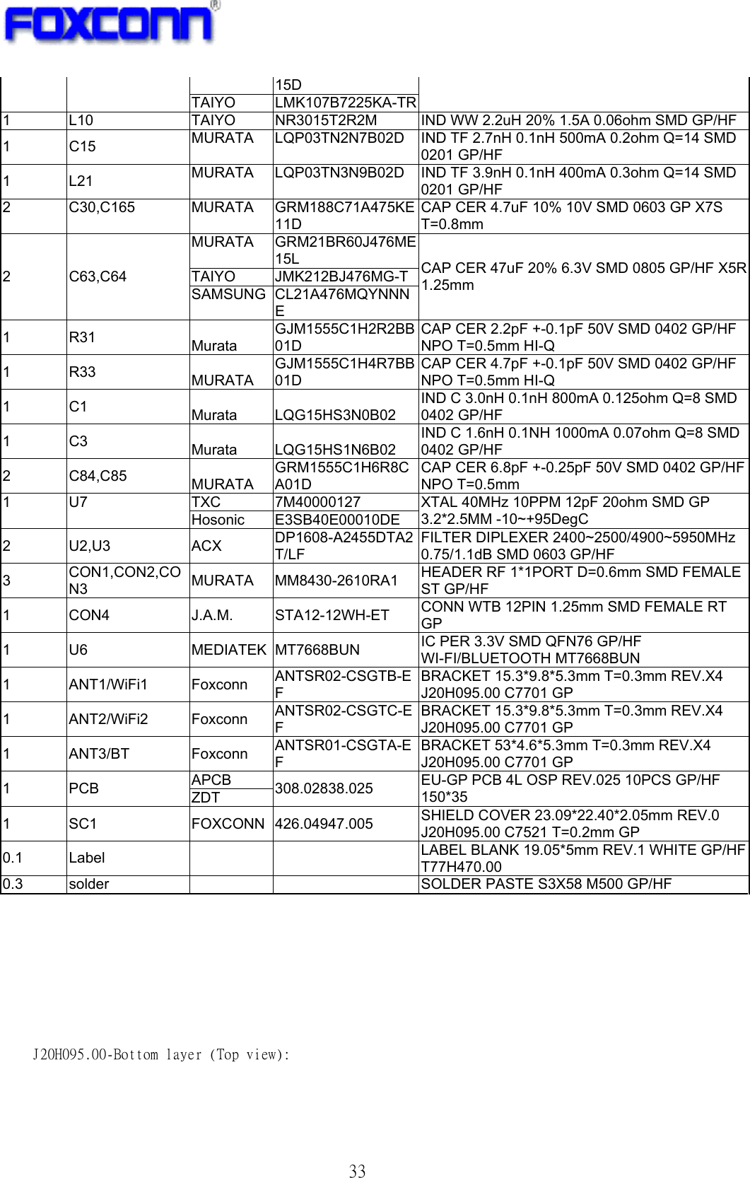
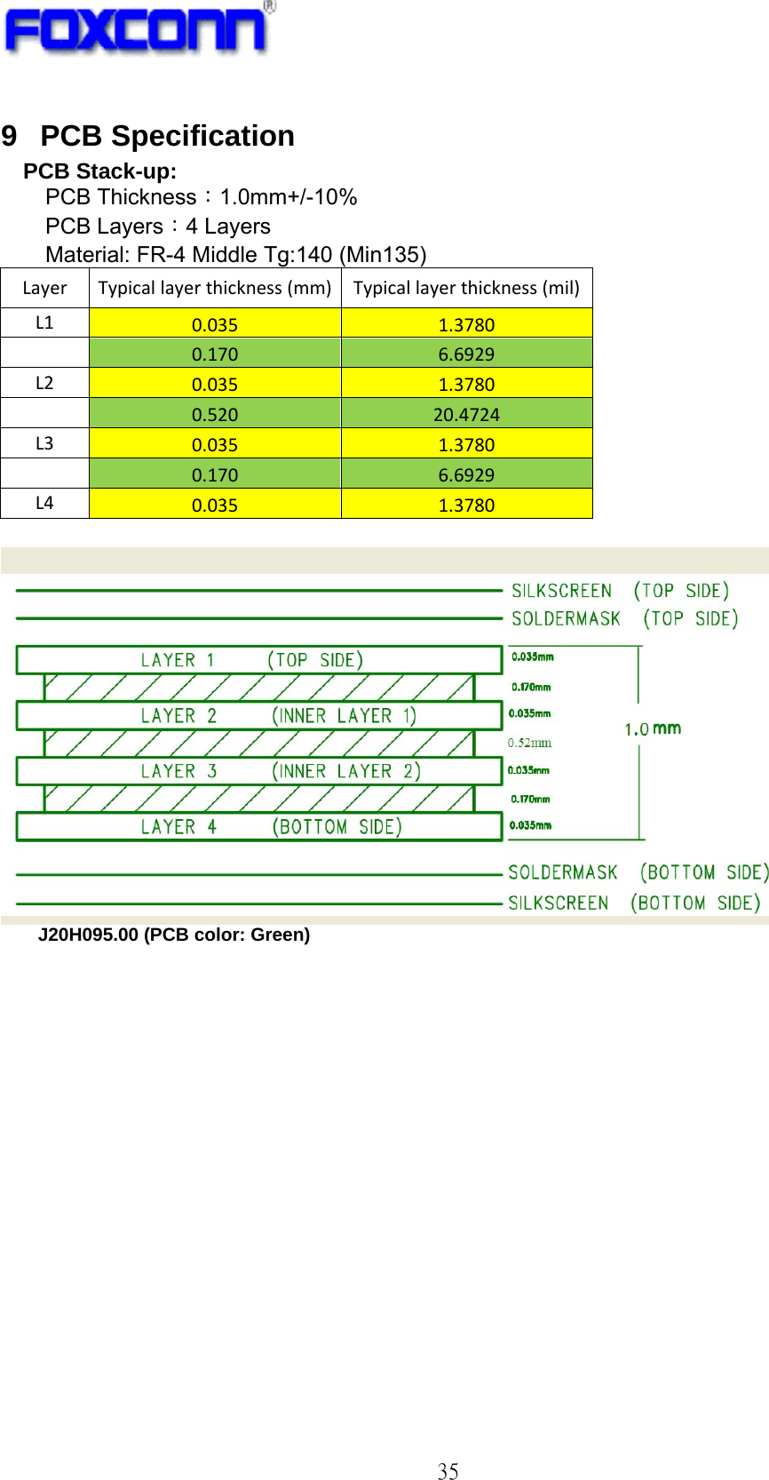
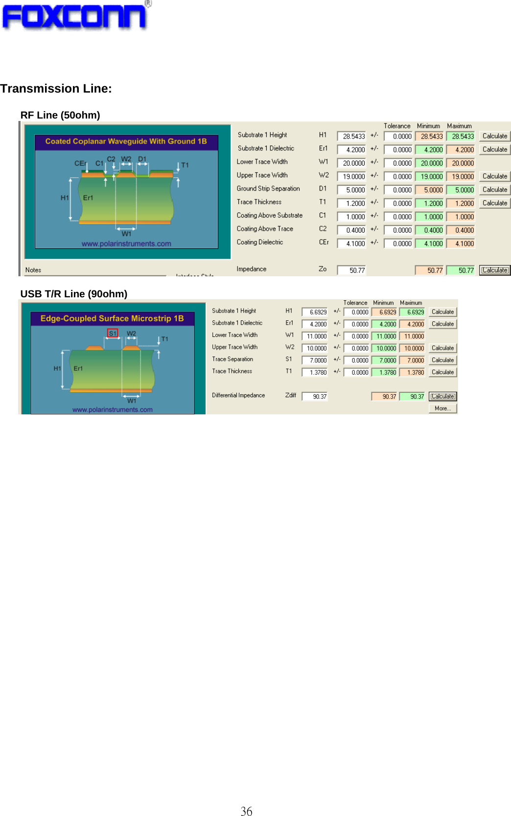
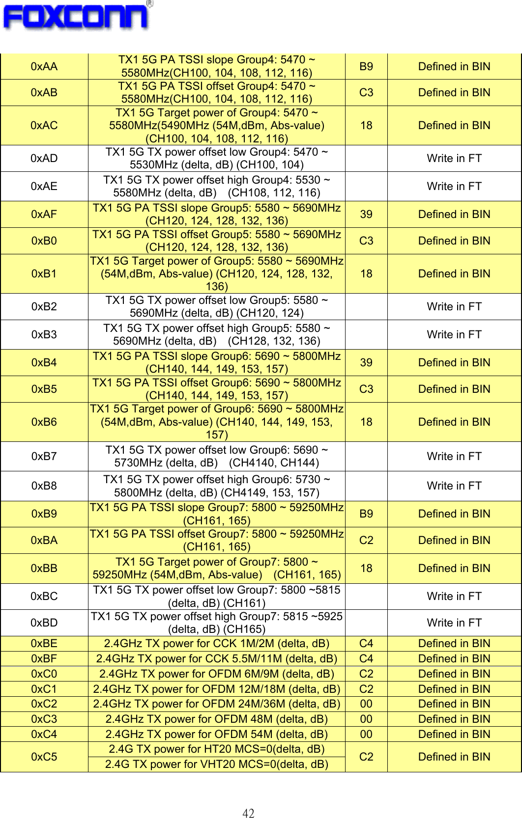
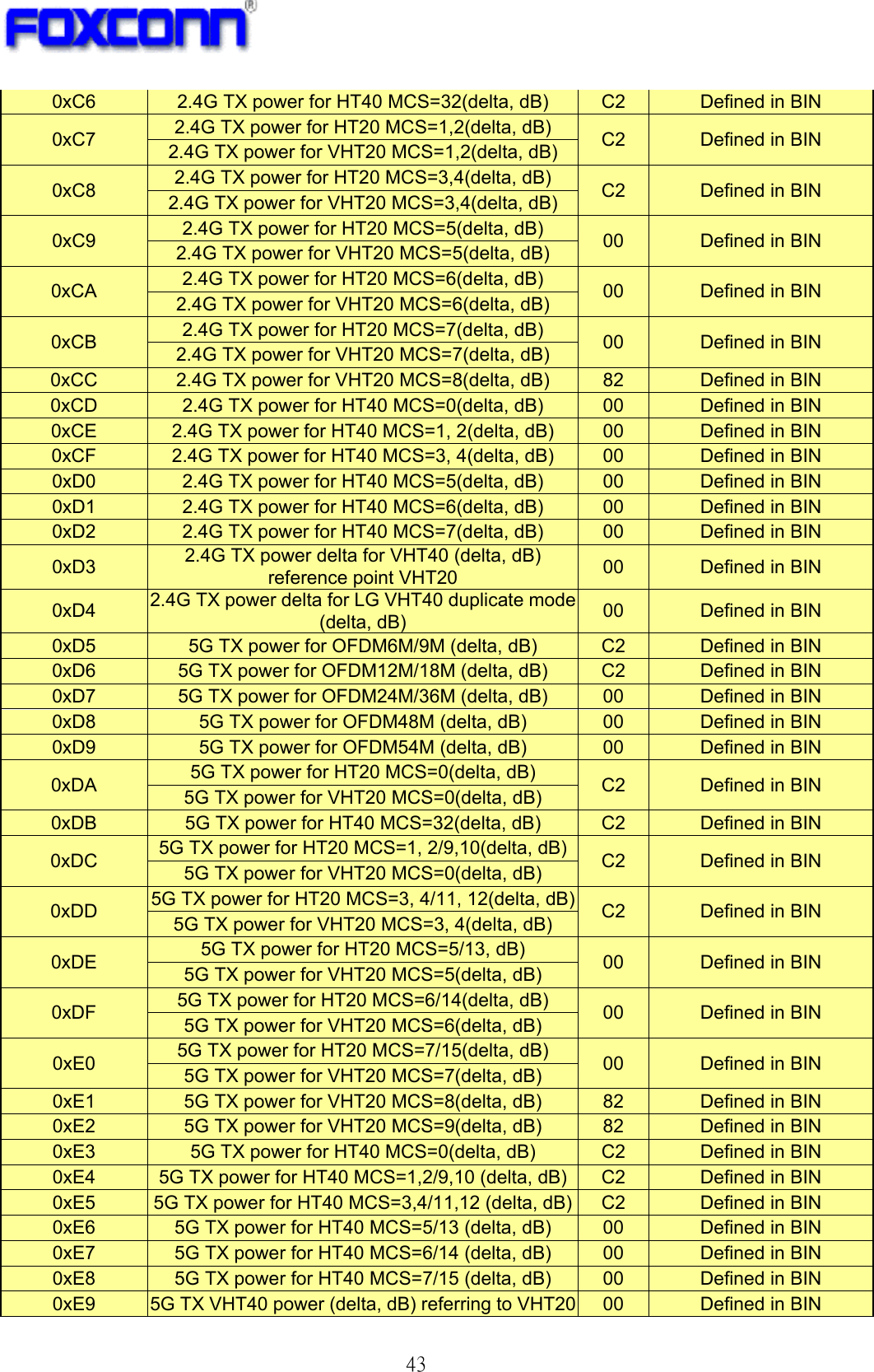
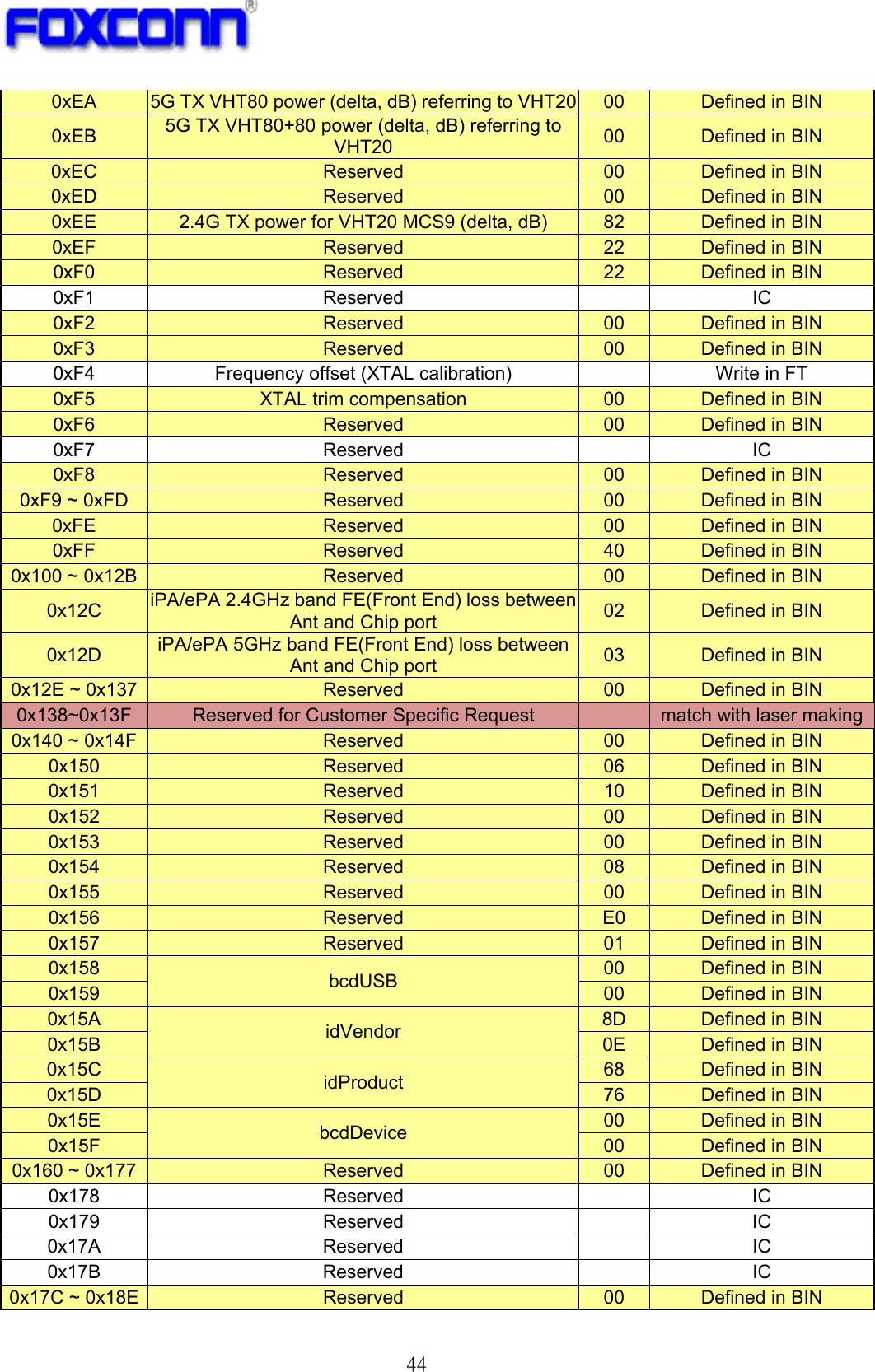
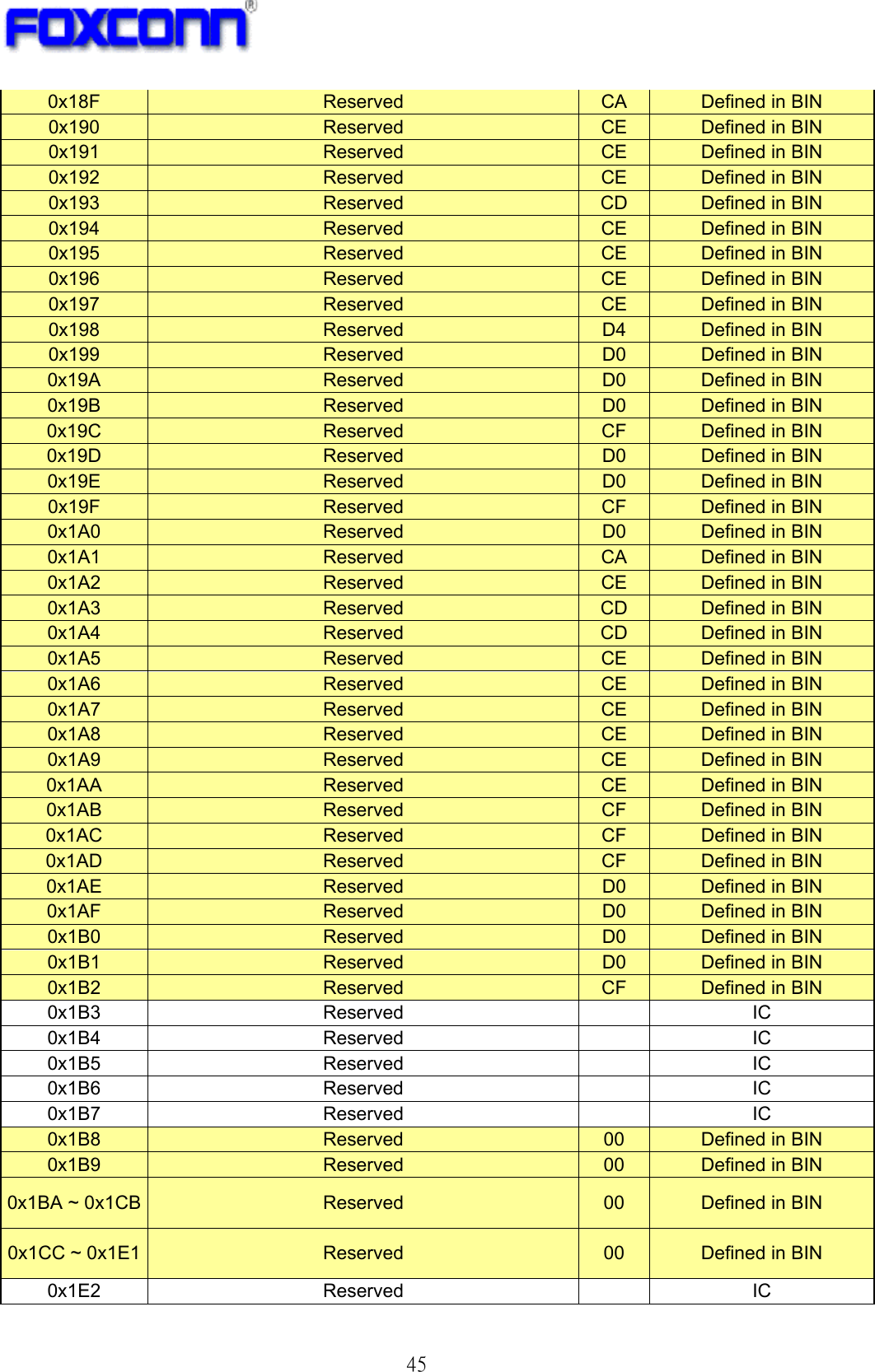
Sony Group J20H095 WLAN/BT Module User Manual 802
Sony Corporation WLAN/BT Module 802
UserManual.wiki
>
Sony Group
>
J20H095 User Manual
Users Manual rev.pdf
Navigation menu
Upload a User Manual
Namespaces
Wiki Guide
HTML
PDF
Info
Views
User Manual
Discussion / Help
Navigation


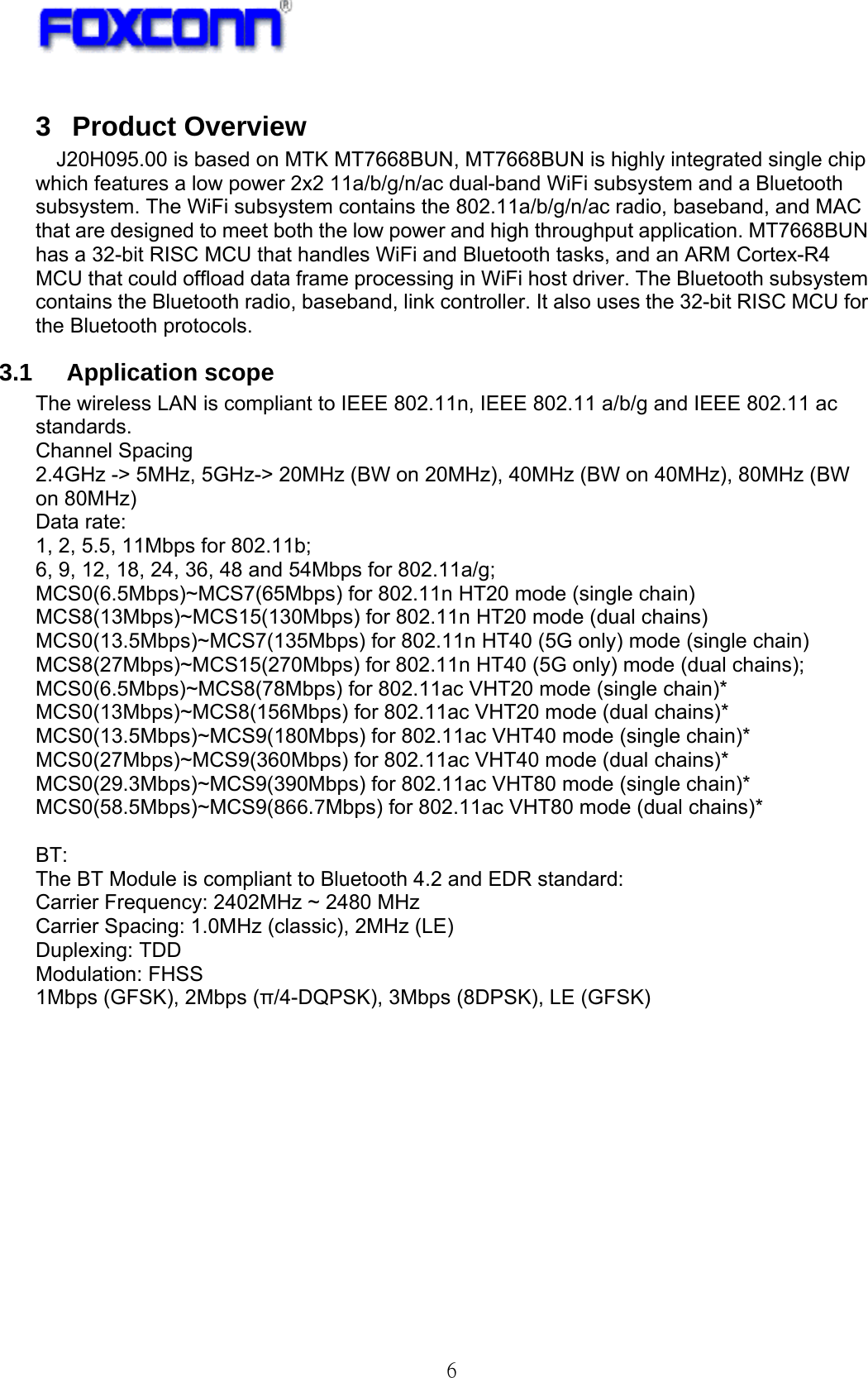
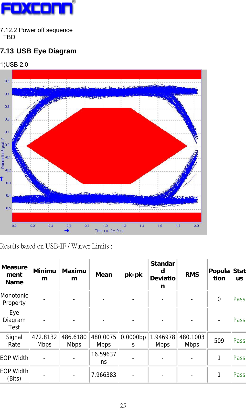
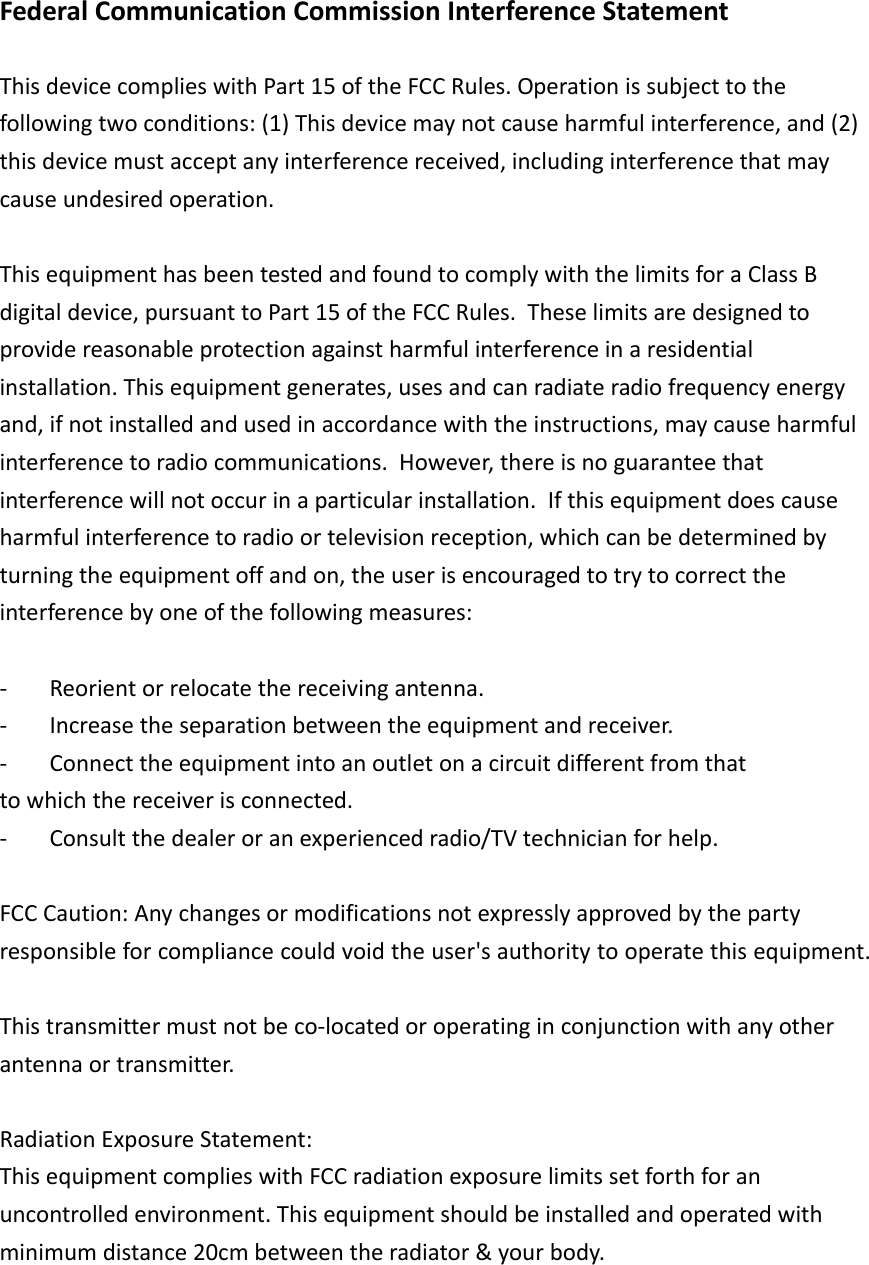
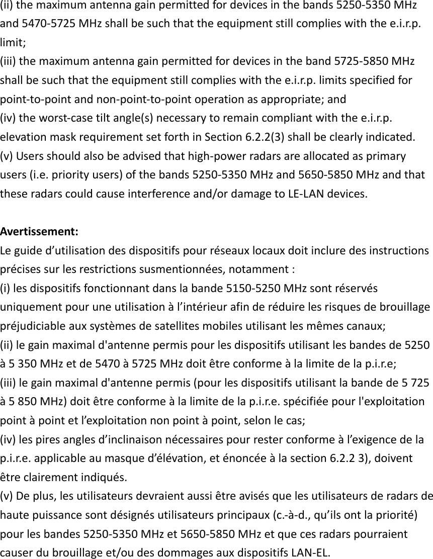
![27 Paired JK Jitter -419.5018ps 301.5176ps 5.597451ps 721.0195ps 242.5373ps 221.4760ps 6 PassPaired KJ Jitter -408.5133ps 331.1229ps 0.0000s 739.6362ps 250.7989ps 234.6009ps 8 Pass 7.14 Antenna Electrical Specification ANT1 (Free space) Peak gain: Wi-Fi ANT1 2.4GHz 5GHz ch Freq [MHz] Peak Gain [dBi] ch Freq [MHz] Peak Gain[dBi] 1 2412 -2.69 W52 36 5180 -0.62 2 2417 -2.49 40 5200 -0.35 3 2422 -2.37 44 5220 0.33 4 2427 -2.25 48 5240 0.45 5 2432 -2.19 W53 52 5260 0.87 6 2437 -2.20 56 5280 1.14 7 2442 -2.08 60 5300 0.99 8 2447 -1.94 64 5320 0.69 9 2452 -1.81 W56 100 5500 0.33 10 2457 -1.72 104 5520 0.34 11 2462 -1.38 108 5540 0.27 12 2467 -1.10 112 5560 0.17 13 2472 -0.84 116 5580 -0.01 120 5600 -0.60 124 5620 -1.21 128 5640 -1.85 132 5660 -2.07 136 5680 -1.67 140 5700 -1.26 ANT2 (Free space) Peak gain: Wi-Fi ANT2 2.4GHz 5GHz ch Freq [MHz] Peak Gain [dBi] ch Freq [MHz] Peak Gain[dBi]](https://usermanual.wiki/Sony-Group/J20H095/User-Guide-3622334-Page-27.png)
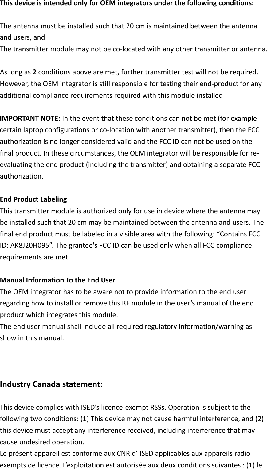
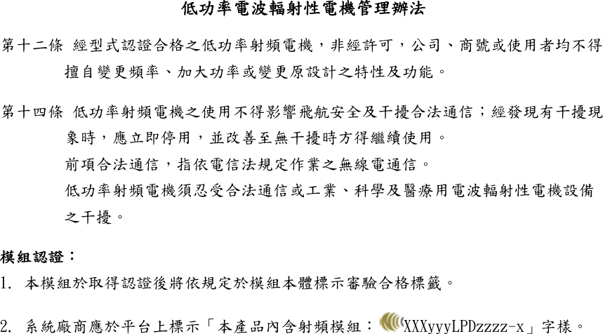
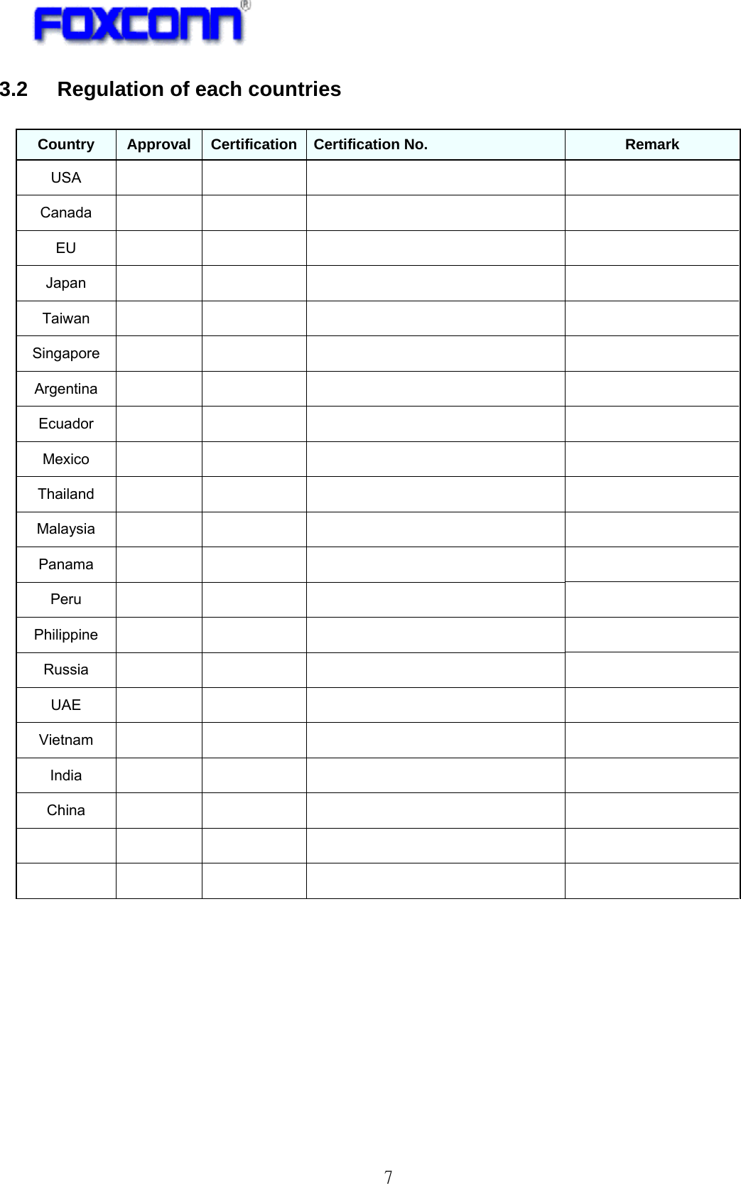
![ch Freq[MHz]PeakGainFreq[MHz]PeakGain ch Freq[MHz]PeakGainFreq[MHz]PeakGain ch Freq[MHz]PeakGain ch Freq[MHz]PeakGain ch Freq[MHz]PeakGain1 2412 0.96 36 5180 1.74 1 2412 -2.69 36 5180 -0.62 1 2402 4.23 28 24293.80 55 24563.222 2417 1.42 40 5200 2.06 2 2417 -2.49 40 5200 -0.35 2 2403 4.20 29 24303.78 56 24573.193 2422 1.70 44 5220 2.61 3 2422 -2.37 44 5220 0.33 3 2404 4.18 30 24313.76 57 24583.164 2427 2.12 48 52403.21 4 2427 -2.25 48 5240 0.45 4 2405 4.17 31 24323.73 58 24593.115 2432 2.46 52 52603.67 5 2432 -2.19 52 5260 0.87 5 2406 4.16 32 24333.71 59 24603.046 2437 2.64 56 52803.67 6 2437 -2.20 56 5280 1.14 6 2407 4.16 33 24343.69 60 2461 2.987 2442 2.99 60 53003.32 7 2442 -2.08 60 5300 0.99 7 2408 4.15 34 24353.67 61 2462 2.908 24473.27 64 53203.19 8 2447 -1.94 64 5320 0.69 8 2409 4.05 35 24363.64 62 2463 2.839 24523.35 100 5500 2.90 9 2452 -1.81 100 5500 0.33 9 2410 4.05 36 24373.63 63 2464 2.7710 24573.63 104 55203.23 10 2457 -1.72 104 5520 0.34 10 2411 4.08 37 24383.61 64 2465 2.7411 24623.58 108 55403.56 11 2462 -1.38 108 5540 0.27 11 2412 4.09 38 24393.61 65 2466 2.7212 24673.72 112 55603.56 12 2467 -1.10 112 5560 0.17 12 2413 4.11 39 24403.61 66 2467 2.7313 24723.87 116 55803.36 13 2472 -0.84 116 5580 -0.01 13 2414 4.11 40 24413.61 67 2468 2.73120 5600 2.99 120 5600 -0.60 14 2415 4.10 41 24423.59 68 2469 2.72124 5620 2.81 124 5620 -1.21 15 2416 4.07 42 24433.58 69 2470 2.72128 5640 2.67 128 5640 -1.85 16 2417 4.03 43 24443.57 70 2471 2.69132 5660 2.68 132 5660 -2.07 17 24183.99 44 24453.55 71 2472 2.65136 5680 2.80 136 5680 -1.67 18 24193.95 45 24463.52 72 2473 2.61140 5700 2.81 140 5700 -1.26 19 24203.92 46 24473.49 73 2474 2.55149 5745 2.84 149 5745 -1.14 20 24213.90 47 24483.44 74 2475 2.49153 5765 2.78 153 5765 -0.66 21 24223.86 48 24493.40 75 2476 2.43157 57853.04 157 5785 -0.44 22 24233.82 49 24503.35 76 2477 2.37161 58053.38 161 5805 -0.13 23 24243.81 50 24513.31 77 2478 2.38165 58253.25 165 5825 -0.64 24 24253.80 51 24523.29 78 2479 2.3725 24263.81 52 24533.28 79 2480 2.3726 24273.82 53 24543.2627 24283.81 54 24553.24W53W56chW58 W58BluetoothWi-Fi ANT22.4GHz帯 5GHz帯W52W53W56Wi-Fi ANT12.4GHz帯 5GHz帯chW52](https://usermanual.wiki/Sony-Group/J20H095/User-Guide-3622334-Page-28.png)

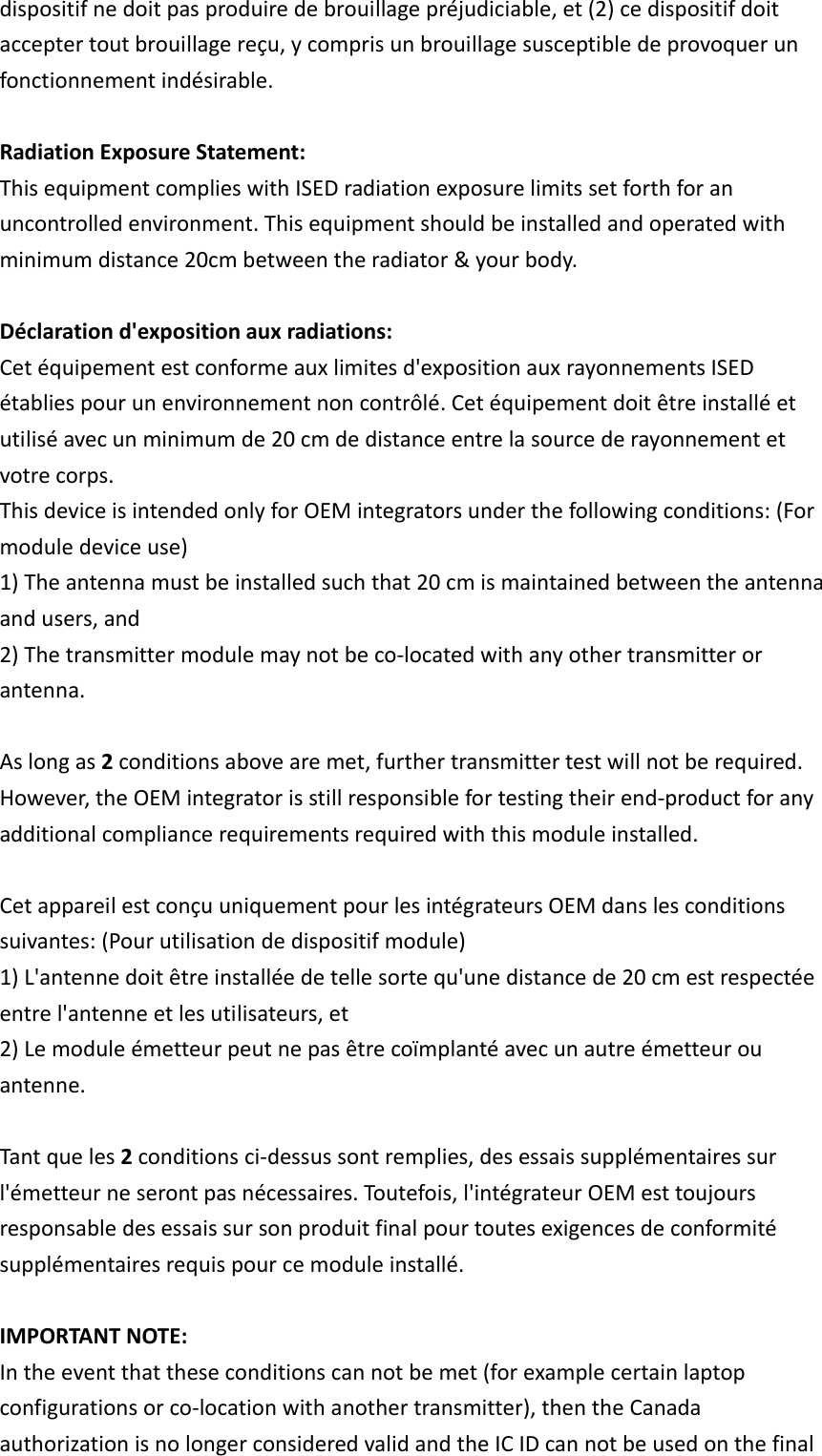
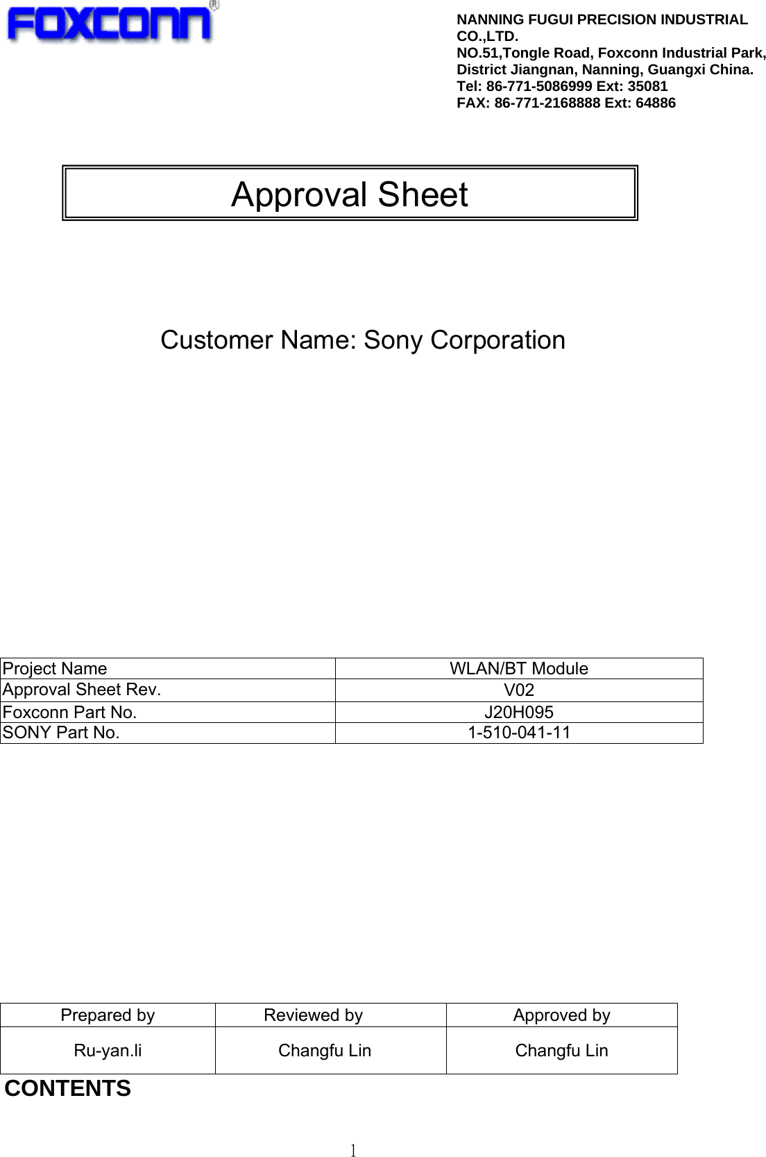
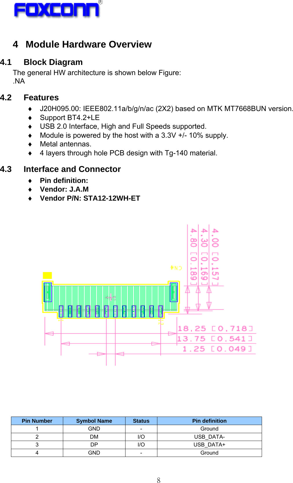
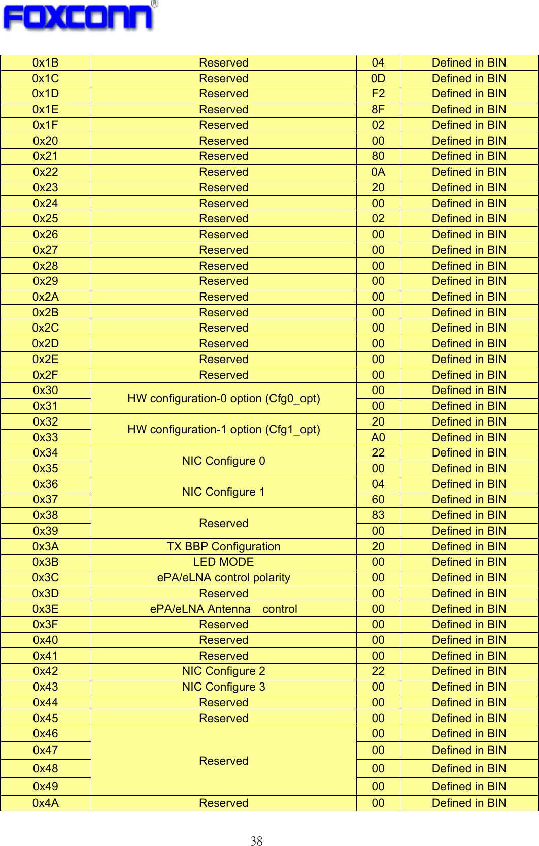
![37 12 OTP content User Area (0x138~0X13F) Index Description Value Efuse Location content ZZ Serial Number (High) It starts from 1 in each line every morning. It will be incremented by one. Ex. Serial Number = 32 (Decade) 0xZZ=0x00, 0xZZ=0x20,range:0001-FFFF 0x138 TBD ZZ Serial Number (Low) 0x139 TBD YY Year Year (0x11=>2017,0x12=>2018,0x13=>2019) 0x13A 11 MM Month Month (range : 0x01-0x0C) 0x13B 07 DD Date Date (range : 0x01-0x1F) 0x13C TBD LL Line Number Line Number (range : 0x01 -0xFF) 0x13D TBD N Module Identification Print “0” 0x13E 00 C Region code Print “0” HH Hardware Version 2 Trial and Revision Number for TV Module 0x13F 04 00=ES1 01=ES2 02=ES3 03=ES4 04=MVT 05=MP 06~0FF=Reserved Efuse Map Offset Description value value Type 0x00 Chip ID 68 Defined in BIN 0x01 76 Defined in BIN 0x02 E-fuse Version 00 Defined in BIN 0x03 00 Defined in BIN 0x04 1st WLAN Mac Address [7:0] match with laser making0x05 1st WLAN Mac Address [15:8] match with laser making0x06 1st WLAN Mac Address [23:16] match with laser making0x07 1st WLAN Mac Address [31:24] match with laser making0x08 1st WLAN Mac Address [39:32] match with laser making0x09 1st WLAN Mac Address [47:40] match with laser making0x0A Reserved 68 Defined in BIN 0x0B Reserved 76 Defined in BIN 0x0C Reserved C3 Defined in BIN 0x0D Reserved 14 Defined in BIN 0x0E Reserved 00 Defined in BIN 0x0F Reserved 00 Defined in BIN 0x10 Reserved 80 Defined in BIN 0x11 Reserved 02 Defined in BIN 0x12 Reserved C3 Defined in BIN 0x13 Reserved 14 Defined in BIN 0x14 Reserved 15 Defined in BIN 0x15 Reserved 76 Defined in BIN 0x16 Reserved 03 Defined in BIN 0x17 Reserved 22 Defined in BIN 0x18 Reserved FF Defined in BIN 0x19 Reserved FF Defined in BIN 0x1A Reserved 23 Defined in BIN](https://usermanual.wiki/Sony-Group/J20H095/User-Guide-3622334-Page-36.png)
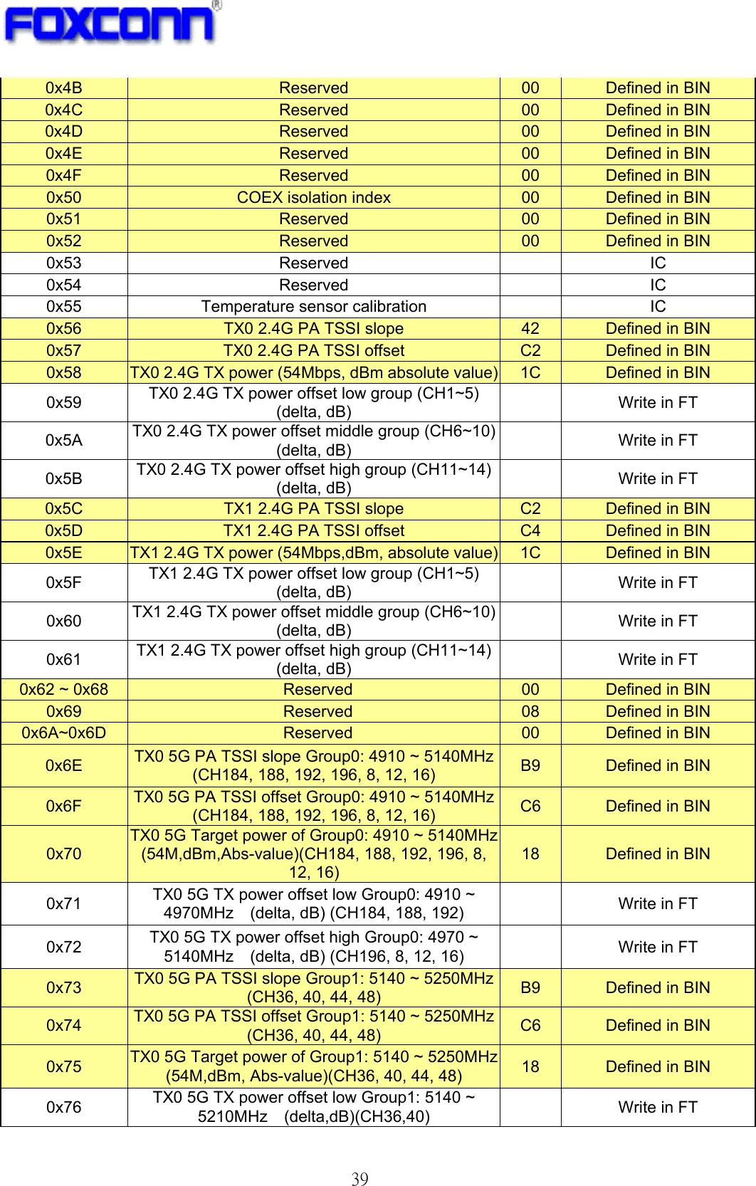
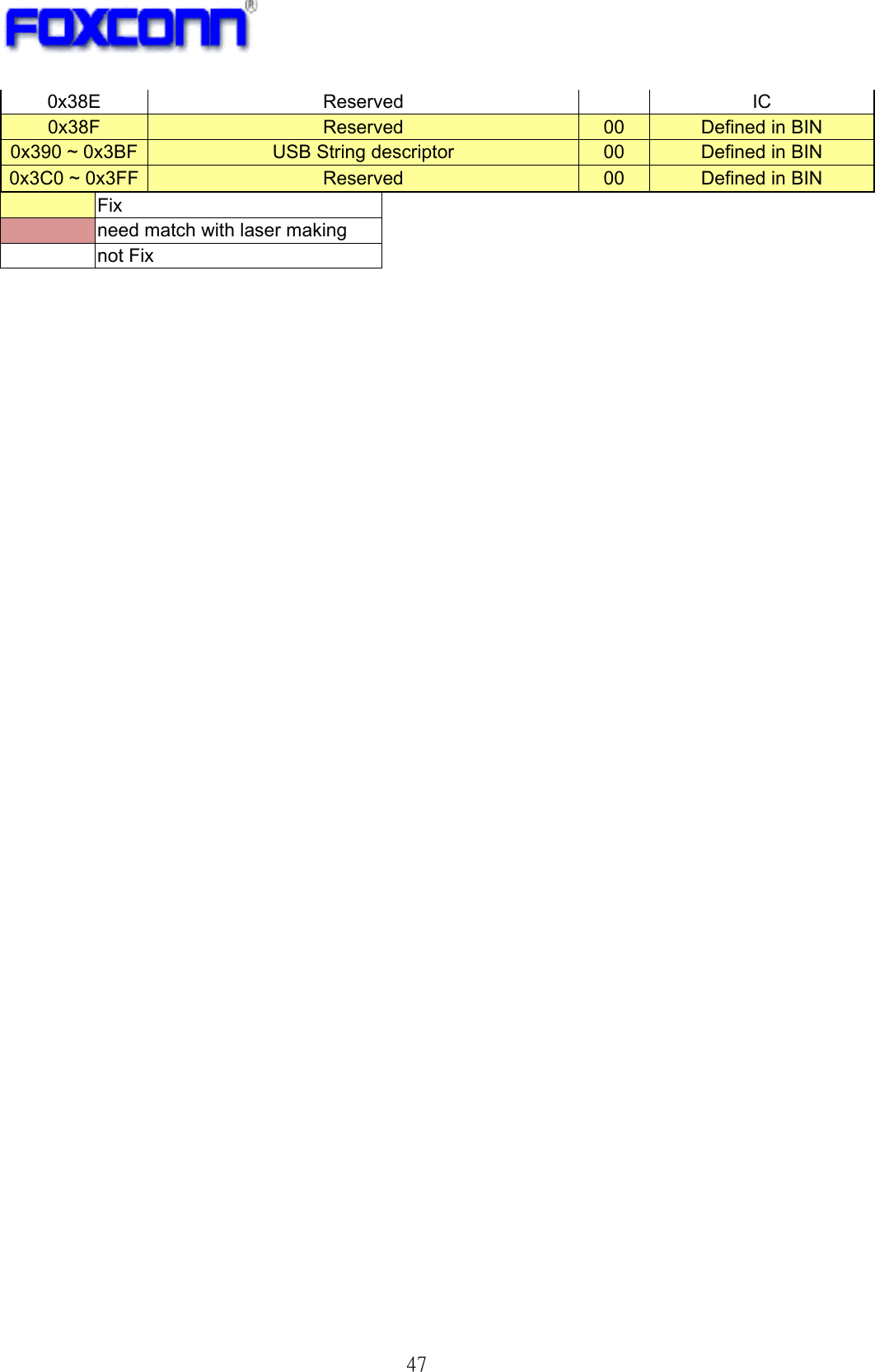
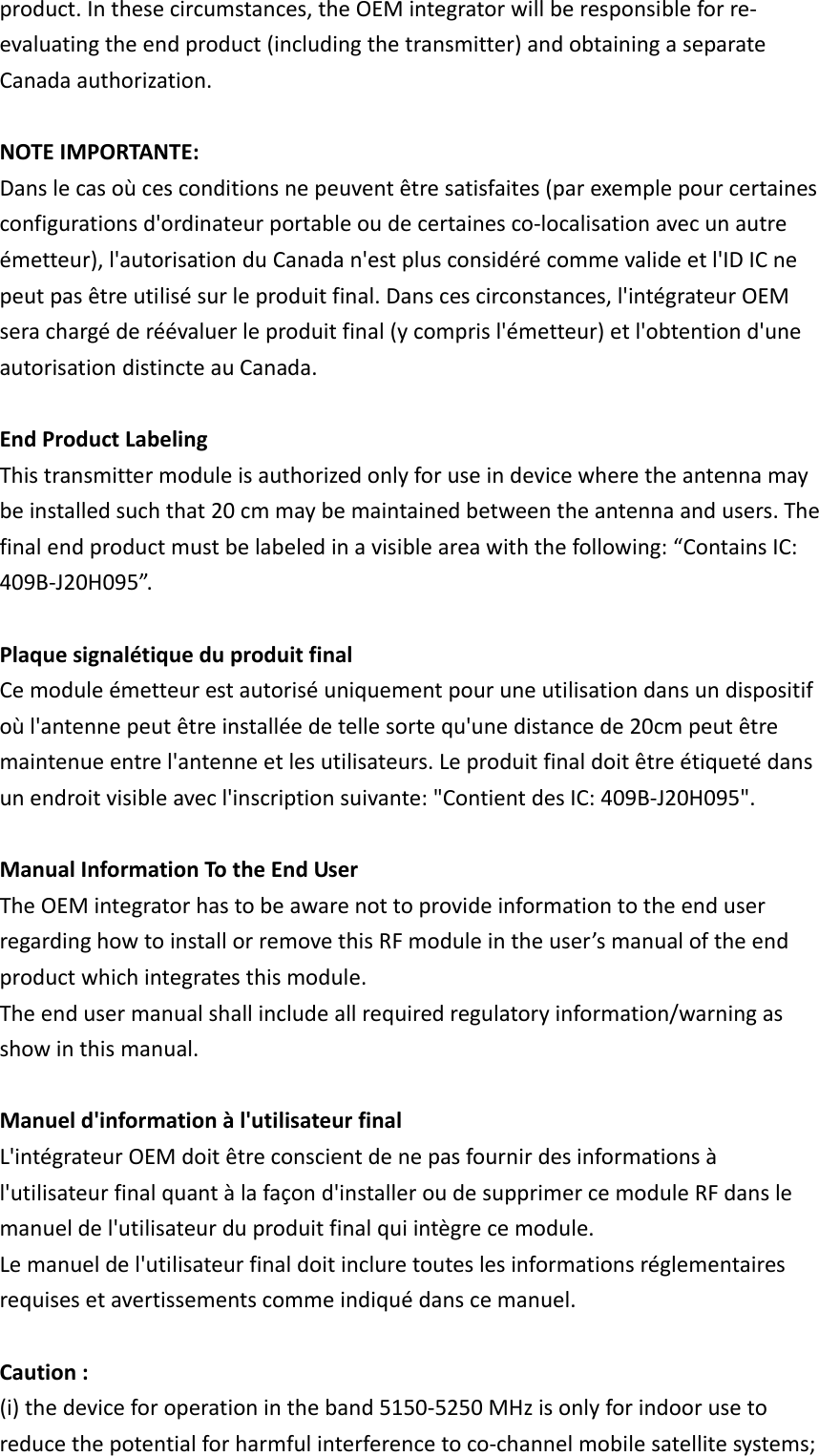
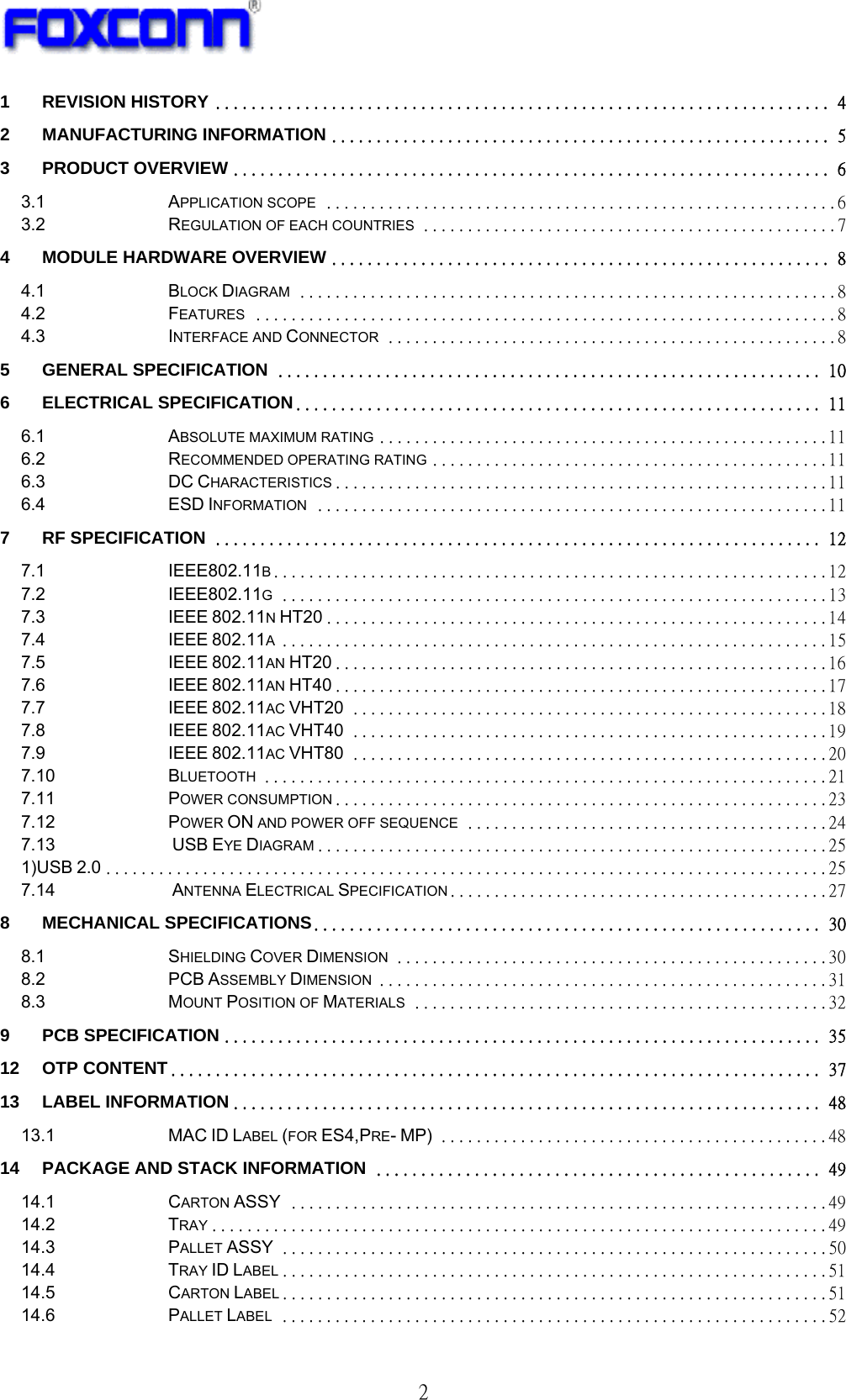
![46 0x1E3 Reserved IC 0x1E4 ~ 0x2FF Reserved 00 Defined in BIN 0x300 Reserved IC 0x301 ~ 0x304 Reserved 00 Defined in BIN 0x305 Reserved IC 0x306 Reserved IC 0x307 Reserved IC 0x308 Reserved IC 0x309 Reserved IC 0x30A 2nd WLAN Mac Address [7:0] 00 Defined in BIN 0x30B 2nd WLAN Mac Address [15:8] 00 Defined in BIN 0x30C 2nd WLAN Mac Address [23:16] 00 Defined in BIN 0x30D 2nd WLAN Mac Address [31:24] 00 Defined in BIN 0x30E 2nd WLAN Mac Address [39:32] 00 Defined in BIN 0x30F 2nd WLAN Mac Address [47:40] 00 Defined in BIN 0x310 ~ 0x33F Reserved 00 Defined in BIN 0x340~0x343 Reserved 02 Defined in BIN 0x344 Reserved 24 Defined in BIN 0x345~0x347 Reserved 04 Defined in BIN 0x348 Reserved 40 Defined in BIN 0x349~0x34B Reserved 03 Defined in BIN 0x34C Reserved 40 Defined in BIN 0x34D~0x34F Reserved 20 Defined in BIN 0x350~0x365 Reserved 00 Defined in BIN 0x366 ~ 0x36C Reserved IC 0x36D BT TX power by-channel compensation (Group 1, 2400~2414 MHz) Write in FT 0x36E BT TX power by-channel compensation (Group 2, 2415~2427 MHz) Write in FT 0x36F BT TX power by-channel compensation (Group 3, 2428~2440 MHz) Write in FT 0x370 BT TX power by-channel compensation (Group 4, 2441~2453 MHz) Write in FT 0x371 BT TX power by-channel compensation (Group 5, 2454~2466 MHz) Write in FT 0x372 BT TX power by-channel compensation (Group 6, 2467~2484 MHz) Write in FT 0x373 ~ 0x381 Reserved 00 Defined in BIN 0x382 BT TX Power level setting 66 Defined in BIN 0x383 BR/EDR/BLE TX Power setting 76 Defined in BIN 0x384 BT MAC Address [7:0] match with laser making0x385 BT MAC Address [15:8] match with laser making0x386 BT MAC Address [23:16] match with laser making0x387 BT MAC Address [31:24] match with laser making0x388 BT MAC Address [39:32] match with laser making0x389 BT MAC Address [47:40] match with laser making0x38A ~ 0x38B Reserved 00 Defined in BIN 0x38C Reserved IC 0x38D Reserved IC](https://usermanual.wiki/Sony-Group/J20H095/User-Guide-3622334-Page-45.png)