Sony Group J20H095 WLAN/BT Module User Manual 802
Sony Corporation WLAN/BT Module 802
Users Manual rev.pdf

1
Customer Name: Sony Corporation
Project Name WLAN/BT Module
Approval Sheet Rev. V02
Foxconn Part No. J20H095
SONY Part No. 1-510-041-11
Prepared by Reviewed by Approved by
Ru-yan.li Changfu Lin Changfu Lin
CONTENTS
NANNING FUGUI PRECISION INDUSTRIAL
CO.,LTD.
NO.51,Tongle Road, Foxconn Industrial Park,
District Jiangnan, Nanning, Guangxi China.
Tel: 86-771-5086999 Ext: 35081
FAX:
86
-
771
-
2168888 Ext: 64886
App
roval Sheet

2
1REVISION HISTORY ..................................................................... 4
2MANUFACTURING INFORMATION ........................................................ 5
3PRODUCT OVERVIEW ................................................................... 6
3.1APPLICATION SCOPE .......................................................... 6
3.2REGULATION OF EACH COUNTRIES ............................................... 7
4MODULE HARDWARE OVERVIEW ........................................................ 8
4.1BLOCK DIAGRAM ............................................................. 8
4.2FEATURES .................................................................. 8
4.3INTERFACE AND CONNECTOR ................................................... 8
5GENERAL SPECIFICATION ............................................................. 10
6ELECTRICAL SPECIFICATION ........................................................... 11
6.1ABSOLUTE MAXIMUM RATING ................................................... 11
6.2RECOMMENDED OPERATING RATING ............................................. 11
6.3DC CHARACTERISTICS ........................................................ 11
6.4ESD INFORMATION .......................................................... 11
7RF SPECIFICATION .................................................................... 12
7.1IEEE802.11B ............................................................... 12
7.2IEEE802.11G .............................................................. 13
7.3IEEE 802.11N HT20 ......................................................... 14
7.4IEEE 802.11A .............................................................. 15
7.5IEEE 802.11AN HT20 ........................................................ 16
7.6IEEE 802.11AN HT40 ........................................................ 17
7.7IEEE 802.11AC VHT20 ...................................................... 18
7.8IEEE 802.11AC VHT40 ...................................................... 19
7.9IEEE 802.11AC VHT80 ...................................................... 20
7.10BLUETOOTH ................................................................ 21
7.11POWER CONSUMPTION ........................................................ 23
7.12POWER ON AND POWER OFF SEQUENCE ......................................... 24
7.13 USB EYE DIAGRAM .......................................................... 25
1)USB 2.0 .................................................................................. 25
7.14 ANTENNA ELECTRICAL SPECIFICATION ........................................... 27
8MECHANICAL SPECIFICATIONS......................................................... 30
8.1SHIELDING COVER DIMENSION ................................................. 30
8.2PCB ASSEMBLY DIMENSION ................................................... 31
8.3MOUNT POSITION OF MATERIALS ............................................... 32
9PCB SPECIFICATION ................................................................... 35
12OTP CONTENT ......................................................................... 37
13LABEL INFORMATION .................................................................. 48
13.1MAC ID LABEL (FOR ES4,PRE- MP) ............................................ 48
14PACKAGE AND STACK INFORMATION .................................................. 49
14.1CARTON ASSY ............................................................. 49
14.2TRAY ...................................................................... 49
14.3PALLET ASSY .............................................................. 50
14.4TRAY ID LABEL .............................................................. 51
14.5CARTON LABEL .............................................................. 51
14.6PALLET LABEL .............................................................. 52


4
1 Revision History
Date Document
revision Change Description
2017/06/27 01
Initial release
2017/09/04 02
Add customer PN

5
2 Manufacturing Information
Manufacture Country:
Made in China
Manufacturer:
NANNING FUGUI PRECISION INDUSTRIAL CO.,LTD.
Manufacture Address:
NO.51,Tongle Road, Foxconn Industrial Park, District Jiangnan, Nanning,
Guangxi China.

6
3 Product Overview
J20H095.00 is based on MTK MT7668BUN, MT7668BUN is highly integrated single chip
which features a low power 2x2 11a/b/g/n/ac dual-band WiFi subsystem and a Bluetooth
subsystem. The WiFi subsystem contains the 802.11a/b/g/n/ac radio, baseband, and MAC
that are designed to meet both the low power and high throughput application. MT7668BUN
has a 32-bit RISC MCU that handles WiFi and Bluetooth tasks, and an ARM Cortex-R4
MCU that could offload data frame processing in WiFi host driver. The Bluetooth subsystem
contains the Bluetooth radio, baseband, link controller. It also uses the 32-bit RISC MCU for
the Bluetooth protocols.
3.1 Application scope
The wireless LAN is compliant to IEEE 802.11n, IEEE 802.11 a/b/g and IEEE 802.11 ac
standards.
Channel Spacing
2.4GHz -> 5MHz, 5GHz-> 20MHz (BW on 20MHz), 40MHz (BW on 40MHz), 80MHz (BW
on 80MHz)
Data rate:
1, 2, 5.5, 11Mbps for 802.11b;
6, 9, 12, 18, 24, 36, 48 and 54Mbps for 802.11a/g;
MCS0(6.5Mbps)~MCS7(65Mbps) for 802.11n HT20 mode (single chain)
MCS8(13Mbps)~MCS15(130Mbps) for 802.11n HT20 mode (dual chains)
MCS0(13.5Mbps)~MCS7(135Mbps) for 802.11n HT40 (5G only) mode (single chain)
MCS8(27Mbps)~MCS15(270Mbps) for 802.11n HT40 (5G only) mode (dual chains);
MCS0(6.5Mbps)~MCS8(78Mbps) for 802.11ac VHT20 mode (single chain)*
MCS0(13Mbps)~MCS8(156Mbps) for 802.11ac VHT20 mode (dual chains)*
MCS0(13.5Mbps)~MCS9(180Mbps) for 802.11ac VHT40 mode (single chain)*
MCS0(27Mbps)~MCS9(360Mbps) for 802.11ac VHT40 mode (dual chains)*
MCS0(29.3Mbps)~MCS9(390Mbps) for 802.11ac VHT80 mode (single chain)*
MCS0(58.5Mbps)~MCS9(866.7Mbps) for 802.11ac VHT80 mode (dual chains)*
BT:
The BT Module is compliant to Bluetooth 4.2 and EDR standard:
Carrier Frequency: 2402MHz ~ 2480 MHz
Carrier Spacing: 1.0MHz (classic), 2MHz (LE)
Duplexing: TDD
Modulation: FHSS
1Mbps (GFSK), 2Mbps (π/4-DQPSK), 3Mbps (8DPSK), LE (GFSK)

7
3.2 Regulation of each countries
Country Approval Certification Certification No. Remark
USA
Canada
EU
Japan
Taiwan
Singapore
Argentina
Ecuador
Mexico
Thailand
Malaysia
Panama
Peru
Philippine
Russia
UAE
Vietnam
India
China
8
4 Module Hardware Overview
4.1 Block Diagram
The general HW architecture is shown below Figure:
.NA
4.2 Features
♦ J20H095.00: IEEE802.11a/b/g/n/ac (2X2) based on MTK MT7668BUN version.
♦ Support BT4.2+LE
♦ USB 2.0 Interface, High and Full Speeds supported.
♦ Module is powered by the host with a 3.3V +/- 10% supply.
♦ Metal antennas.
♦ 4 layers through hole PCB design with Tg-140 material.
4.3 Interface and Connector
♦ Pin definition:
♦ Vendor: J.A.M
♦ Vendor P/N: STA12-12WH-ET
Pin Number Symbol Name Status Pin definition
1 GND - Ground
2 DM I/O USB_DATA-
3 DP I/O USB_DATA+
4 GND - Ground

9
5 VCC PWR DC +3.3V
6 VCC PWR DC +3.3V
7 VCC PWR DC +3.3V
8 GND - Ground
9 GND - Ground
10 WOW_L Output
Wake on WLAN signal output
"L"-drive is hoped when awake Host
11 RST_L Input "L"-drive reset signal input from Host
12 GND - Ground
S1 GND - Ground
S2 GND - Ground

10
5 General Specification
Item Specification
Frequency Range 2412MHz~2462MHz
5180MHz~5240MHz
5260MHz~5320MHz
5500MHz~5700MHz
5745MHz~5825MHz
Shielding Case Temperature (Figure 1) ~83.46℃@Ta=65℃
PCB Case Temperature (Figure 2) ~97.92℃@Ta=65℃
IC Case Measurement Temperature (Figure 3) ~102.33℃@Ta=65℃
Maximum Ripple on Supplied Voltage TBD
Antenna Port Impedance 50 ohm typ.
VSWR Antenna 1 <3
(with TV platform) Antenna 2 <3
Antenna 3 <3
Temperature Operating Temperature
-10℃~65℃
Storage Temperature
-40℃~85℃
Humidity Storage Humidity 45%~70% (Non-condensing)
11
6 Electrical Specification
6.1 Absolute maximum rating
6.2 Recommended operating rating
Element Symbol Min Typ Max Unit
DC supply voltage VDD33 2.97 3.3
3.63 (V)
6.3 DC Characteristics
Parameter Min Typ. Max Unit
Supply voltage 2.97 3.3 3.63 (V)
2.412GHz Tx Current(1M/16dBm) 483.3 (mA)
2.412GHz Tx Current(MCS0/15dBm) 460.6 (mA)
5.18GHz Tx Current(6M/13Bm/HT20) 500.6 (mA)
5.19GHz Tx Current(MCS0/13dBm/HT40) 502.5 (mA)
Rx(2G/5GHz) Current 150.3 (mA)
5.21GHz Tx Current(MCS9/11dBm/VHT80)* 375.4 (mA)
Standby 23.9
(mA)
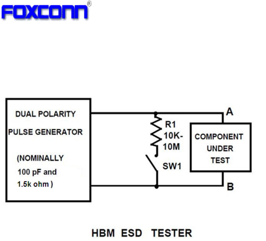
6.4 ESD Information
Mode Level Unit
HBM +/-1500 V
Element Parameter Maximum rating Unit
VDD33 3.3V Supply Voltage -0.3 to 3.63 (V)

12
7 RF Specification
7.1 IEEE802.11b
Items Contents
Specification IEEE802.11b
Mode DSSS / CCK
Channel CH1 to CH13
Data rate 1, 2, 5.5, 11Mbps
Temperature -10℃~65℃
Voltage 3.3V+/-10%
TX Characteristics Min. Typ. Max. Unit
1. Power Levels
1) Target Power@1Mbps 28 dBm
2) Target Power@2Mbps
28 dBm
3) Target Power@5.5Mbps
28 dBm
4) Target Power@11Mbps
28 dBm
2. Spectrum Mask @ target power
1) fc-33MHz < f < fc-22MHz -50 dBr
2) fc-22MHz < f < fc-11MHz -30 dBr
3) fc+11MHz < f < fc+22MHz -30 dBr
4) fc+22MHz < f < fc+33MHz -50 dBr
3. Frequency Error* +20 ppm
4 Modulation Accuracy(EVM)@ target power
1) 1Mbps(peak) -10 dB
2) 2Mbps(peak) -10 dB
3) 5.5Mbps(peak) -10 dB
4) 11Mbps(peak) - - -10 dB
5. Tx spurious emission for all out of band - - -50 dBm
RX Characteristics Min. Typ. Max. Unit
1. Minimum Input Level Sensitivity
1) 1Mbps (FER≦8%) - -97 -92 dBm
2) 2Mbps (FER≦8%) --94 -89 dBm
3) 5.5Mbps (FER≦8%) --92 -87 dBm
4) 11Mbps (FER≦8%) --89 -85 dBm
2. Maximum Input Level (FER≦8%) -10 0 - dBm
3. Adjacent channel rejection
1) 1Mbps (FER≦8%) 35 39 dB
2) 11Mbps (FER≦8%) 35 35 dB
4. Rx spurious emission -63 dBm

13
7.2 IEEE802.11g
Items Contents
Specification IEEE802.11g
Mode OFDM
Channel CH1 to CH13
Data rate 6, 9, 12, 18, 24, 36, 48, 54Mbps
Temperature -10℃~65℃
Voltage 3.3V+/-10%
TX Characteristics Min. Typ. Max. Unit
1. Power Levels
1) Target Power@6Mbps
27 dBm
2) Target Power@9Mbps
27 dBm
3) Target Power@12Mbps
27 dBm
4) Target Power@18Mbps
27 dBm
5) Target Power@24Mbps
26 dBm
6) Target Power@36Mbps
26 dBm
7) Target Power@48Mbps
26 dBm
8) Target Power@54Mbps
26 dBm
2. Spectrum Mask @ target power
1) at fc +/- 11MHz - - -20 dBr
2) at fc +/- 20MHz - - -28 dBr
3) at fc > +/-30MHz - - -40 dBr
3 Modulation Accuracy(EVM)@ target power
1) 6Mbps - -29 -5 dB
2) 9Mbps - -29 -8 dB
3) 12Mbps - -30 -10 dB
4) 18Mbps - -30 -13 dB
5) 24Mbps - -30 -16 dB
6) 36Mbps - -31 -19 dB
7) 48Mbps - -31 -22 dB
8) 54Mbps - -31 -25 dB
4 Frequency Error* -20 - +20 ppm
5.Tx spurious emission for all out of band - - -50 dBm
RX Characteristics Min. Typ. Max. Unit
1. Minimum Input Level Sensitivity
1) 6Mbps (PER <10%) - -94 -83 dBm
2) 9Mbps (PER < 10%) - -92 -81 dBm
3) 12Mbps (PER < 10%) - -91 -79 dBm
4) 18Mbps (PER < 10%) - -87 -77 dBm
5) 24Mbps (PER < 10%) - -85 -75 dBm
6) 36Mbps (PER < 10%) - -80 -73 dBm
7) 48Mbps (PER < 10%) - -77 -71 dBm
8) 54Mbps (PER < 10%) - -75 -69 dBm
2. Maximum Input Level (PER < 10%) -20 -11 - dBm
3. Adjacent channel rejection
1) 6Mbps (PER <10%) 16 39 dB
2) 54Mbps (PER < 10%) -1 23 dB
4. Rx spurious emission -63 dBm

14
7.3 IEEE 802.11n HT20
Items Contents
Specification IEEE802.11n HT20
Mode OFDM
Channel CH1 ~CH13
Data rate (MCS index) MCS0~MCS15
Temperature -10℃~65℃
Voltage 3.3V+/-10%
TX Characteristics Min. Typ. Max. Unit
1. Power Levels
1) Target Power@MCS0
27 dBm
2) Target Power@ MCS1
27 dBm
3) Target Power@ MCS2
27 dBm
4) Target Power@ MCS3
27 dBm
5) Target Power@ MCS4
27 dBm
6) Target Power@ MCS5
26 dBm
7) Target Power@ MCS6
26 dBm
8) Target Power@ MCS7
26 dBm
2. Spectrum Mask @ target power
1) at fc +/- 11MHz - - -20 dBr
2) at fc +/- 20MHz - - -28 dBr
3) at fc > +/-30MHz - - -45 dBr
3. Modulation Accuracy(EVM)@target power
1) MCS0 - -29 -5 dB
2) MCS1 - -29 -10 dB
3) MCS2 - -30 -13 dB
4) MCS3 - -30 -16 dB
5) MCS4 - -30 -19 dB
6) MCS5 - -31 -22 dB
7) MCS6 - -31 -25 dB
8) MCS7 - -31 -28 dB
4. Frequency Error* -20 - +20 ppm
5. Tx spurious emission for all out of band -50 dBm
RX Characteristics Min. Typ. Max. Unit
1. Minimum Input Level Sensitivity
1) MCS0 (PER < 10%) - -94 -81 dBm
2) MCS1 (PER < 10%) - -92 -79 dBm
3) MCS2 (PER < 10%) - -90 -77 dBm
4) MCS3 (PER < 10%) - -86 -75 dBm
5) MCS4 (PER < 10%) - -83 -73 dBm
6) MCS5 (PER < 10%) - -78 -71 dBm
7) MCS6 (PER < 10%) - -76 -69 dBm
8) MCS7 (PER < 10%) - -75 -67 dBm
2. Maximum Input Level (PER < 10%) -20 -10 - dBm
3 Adjacent channel rejection
1) MCS0 (PER <10%) 16 35 dB
2) MCS7 (PER < 10%) -2 8 dB
4. Rx spurious emission -63 dBm

15
7.4 IEEE 802.11a
Items Contents
Specification IEEE802.11a
Mode OFDM
Channel CH36 to CH165
Data rate 6, 9, 12, 18, 24, 36, 48, 54Mbps
Temperature -10℃~65℃
Voltage 3.3V+/-10%
TX Characteristics Min. Typ. Max. Unit
1. Power Levels
1) Target Power@6Mbps
23 dBm
2) Target Power@9Mbps
23 dBm
3) Target Power@12Mbps
23 dBm
4) Target Power@18Mbps
23 dBm
5) Target Power@24Mbps
23 dBm
6) Target Power@36Mbps
23 dBm
7) Target Power@48Mbps
23 dBm
8) Target Power@54Mbps
23 dBm
2. Spectrum Mask @ target power
1) at fc +/- 11MHz - - -20 dBr
2) at fc +/- 20MHz - - -28 dBr
3) at fc > +/-30MHz - - -40 dBr
3 Modulation Accuracy(EVM)@ target power
1) 6Mbps - -30 -5 dB
2) 9Mbps - -30 -8 dB
3) 12Mbps - -31 -10 dB
4) 18Mbps - -31 -13 dB
5) 24Mbps - -31 -16 dB
6) 36Mbps - -32 -19 dB
7) 48Mbps - -32 -22 dB
8) 54Mbps - -32 -25 dB
4 Frequency Error* -20 - +20 ppm
5. Tx spurious emission for all out of band -50 dBm
RX Characteristics Min. Typ. Max. Unit
1. Minimum Input Level Sensitivity
1) 6Mbps (PER <10%) - -92 -83 dBm
2) 9Mbps (PER < 10%) - -91 -81 dBm
3) 12Mbps (PER < 10%) - -90 -79 dBm
4) 18Mbps (PER < 10%) - -87 -77 dBm
5) 24Mbps (PER < 10%) - -85 -75 dBm
6) 36Mbps (PER < 10%) - -80 -73 dBm
7) 48Mbps (PER < 10%) - -77 -71 dBm
8) 54Mbps (PER < 10%) - -75 -69 dBm
2. Maximum Input Level (PER < 10%) -20 -11 - dBm
3. Adjacent channel rejection
1) 6M (PER <10%) 16 29 dB
2) 54M (PER < 10%) -1 15 dB
4. Rx spurious emission -57 dBm

16
7.5 IEEE 802.11an HT20
Items Contents
Specification IEEE802.11an HT20
Mode OFDM
Channel CH36 to CH165
Data rate (MCS index) MCS0~MCS15
Temperature -10℃~65℃
Voltage 3.3V+/-10%
TX Characteristics Min. Typ. Max. Unit
1. Power Levels
1) Target Power@MCS0
23
dBm
2) Target Power@ MCS1
23
dBm
3) Target Power@ MCS2
23
dBm
4) Target Power@ MCS3
23
dBm
5) Target Power@ MCS4
23
dBm
6) Target Power@ MCS5
23
dBm
7) Target Power@ MCS6
23
dBm
8) Target Power@ MCS7
23
dBm
2. Spectrum Mask @ target power
1) at fc +/- 11MHz - - -20 dBr
2) at fc +/- 20MHz - - -28 dBr
3) at fc > +/-30MHz - - -45 dBr
3. Modulation Accuracy(EVM)@ target power
1) MCS0 - -30 -5 dB
2) MCS1 - -30 -10 dB
3) MCS2 - -31 -13 dB
4) MCS3 - -31 -16 dB
5) MCS4 - -31 -19 dB
6) MCS5 - -32 -22 dB
7) MCS6 - -32 -25 dB
8) MCS7 - -32 -28 dB
4. Frequency Error* -20 - +20 ppm
5. Tx spurious emission for all out of band -50 dBm
RX Characteristics Min. Typ. Max. Unit
1. Minimum Input Level Sensitivity
1) MCS0 (PER < 10%) - -91 -81 dBm
2) MCS1 (PER < 10%) - -89 -79 dBm
3) MCS2 (PER < 10%) - -87 -77 dBm
4) MCS3 (PER < 10%) - -84 -75 dBm
5) MCS4 (PER < 10%) - -80 -73 dBm
6) MCS5 (PER < 10%) - -76 -71 dBm
7) MCS6 (PER < 10%) - -74 -69 dBm
8) MCS7 (PER < 10%) - -72 -67 dBm
2. Maximum Input Level (PER < 10%) -20 -10 - dBm
3. Adjacent channel rejection
1) MCS0 (PER <10%) 16 24 dB
2) MCS7 (PER < 10%) -2 3 dB
4. Rx spurious emission -57 dBm

17
7.6 IEEE 802.11an HT40
Items Contents
Specification IEEE802.11an HT40
Mode OFDM
Channel CH38 to CH159
Data rate (MCS index) MCS0~MCS15
Temperature -10℃~65℃
Voltage 3.3V+/-10%
TX Characteristics Min. Typ. Max. Unit
1. Power Levels
1) Target Power@MCS0
23
dBm
2) Target Power@ MCS1
23
dBm
3) Target Power@ MCS2
23
dBm
4) Target Power@ MCS3
23
dBm
5) Target Power@ MCS4
23
dBm
6) Target Power@ MCS5
23
dBm
7) Target Power@ MCS6
23
dBm
8) Target Power@ MCS7
23
dBm
2. Spectrum Mask @ target power
1) at fc +/- 21MHz - - -20 dBr
2) at fc +/- 40MHz - - -28 dBr
3) at fc > +/-60MHz - - -45 dBr
3. Modulation Accuracy(EVM)@ target power
1) MCS0 - -30 -5 dB
2) MCS1 - -30 -10 dB
3) MCS2 - -31 -13 dB
4) MCS3 - -31 -16 dB
5) MCS4 - -31 -19 dB
6) MCS5 - -32 -22 dB
7) MCS6 - -32 -25 dB
8) MCS7 - -32 -28 dB
4. Frequency Error* -20 - +20 ppm
5. Tx spurious emission for all out of band -50 dBm
RX Characteristics Min. Typ. Max. Unit
1. Minimum Input Level Sensitivity
1) MCS0 (PER < 10%) - -89 -78 dBm
2) MCS1 (PER < 10%) - -86 -76 dBm
3) MCS2 (PER < 10%) - -84 -74 dBm
4) MCS3 (PER < 10%) - -81 -72 dBm
5) MCS4 (PER < 10%) - -77 -70 dBm
6) MCS5 (PER < 10%) - -72 -68 dBm
7) MCS6 (PER < 10%) - -71 -66 dBm
8) MCS7 (PER < 10%) - -69 -64 dBm
2. Maximum Input Level (PER < 10%) -20 -10 - dBm
3. Adjacent channel rejection
1) MCS0 (PER <10%) 16 28 dB
2) MCS7 (PER < 10%) -2 5 dB
4. Rx spurious emission -57 dBm

18
7.7 IEEE 802.11ac VHT20
Items Contents
Specification IEEE802.11ac VHT20
Mode OFDM
Channel CH36 to CH165
Data rate (MCS index) MCS0~MCS8 (Nss=1)
Temperature -10℃~65℃
Voltage 3.3V+/-10%
TX Characteristics Min. Typ. Max. Unit
1. Power Levels
1) Target Power@MCS0
23
dBm
2) Target Power@ MCS1
23
dBm
3) Target Power@ MCS2
23
dBm
4) Target Power@ MCS3
23
dBm
5) Target Power@ MCS4
23
dBm
6) Target Power@ MCS5
23
dBm
7) Target Power@ MCS6
23
dBm
8) Target Power@ MCS7
23
dBm
9) Target Power@ MCS8
23 dBm
2. Spectrum Mask @ target power
1) at fc +/- 11MHz - - -20 dBr
2) at fc +/- 20MHz - - -28 dBr
3) at fc > +/-30MHz - - -45 dBr
3. Modulation Accuracy(EVM)@ target power
1) MCS0 - -30 -5 dB
2) MCS1 - -30 -10 dB
3) MCS2 - -31 -13 dB
4) MCS3 - -31 -16 dB
5) MCS4 - -31 -19 dB
6) MCS5 - -32 -22 dB
7) MCS6 - -32 -25 dB
8) MCS7 - -32 -27 dB
9) MCS8 - -32 -30 dB
4. Frequency Error* -20 +20 ppm
5. Tx spurious emission for all out of band -50 dBm
RX Characteristics Min. Typ. Max. Unit
1. Minimum Input Level Sensitivity
1) MCS0 (PER < 10%) - -91 -81 dBm
2) MCS1 (PER < 10%) - -88 -79 dBm
3) MCS2 (PER < 10%) - -87 -77 dBm
4) MCS3 (PER < 10%) - -84 -75 dBm
5) MCS4 (PER < 10%) - -80 -73 dBm
6) MCS5 (PER < 10%) - -75 -71 dBm
7) MCS6 (PER < 10%) - -74 -69 dBm
8) MCS7 (PER < 10%) - -72 -67 dBm
8) MCS8 (PER < 10%) - -68 -58 dBm
2. Maximum Input Level (PER < 10%) -20 -10 - dBm
3. Adjacent channel rejection
1) MCS0 (PER <10%) 16 22 dB
2) MCS8 (PER < 10%) -7 3 dB
4. Rx spurious emission -57 dBm

19
7.8 IEEE 802.11ac VHT40
Items Contents
Specification IEEE802.11ac VHT40
Mode OFDM
Channel CH38 to CH159
Data rate (MCS index) MCS0~MCS9 (Nss=1)
Temperature -10℃~65℃
Voltage 3.3V+/-10%
TX Characteristics Min. Typ. Max. Unit
1. Power Levels
1) Target Power@MCS0
23
dBm
2) Target Power@ MCS1
23
dBm
3) Target Power@ MCS2
23
dBm
4) Target Power@ MCS3
23
dBm
5) Target Power@ MCS4
23
dBm
6) Target Power@ MCS5
23
dBm
7) Target Power@ MCS6
23
dBm
8) Target Power@ MCS7
23
dBm
9) Target Power@ MCS8
23 dBm
10) Target Power@ MCS9
23 dBm
2. Spectrum Mask @ target power
1) at fc +/- 21MHz - - -20 dBr
2) at fc +/- 40MHz - - -28 dBr
3) at fc > +/- 60MHz - - -45 dBr
3. Modulation Accuracy(EVM)@ target power
1) MCS0 - -30 -5 dB
2) MCS1 - -30 -10 dB
3) MCS2 - -31 -13 dB
4) MCS3 - -31 -16 dB
5) MCS4 - -31 -19 dB
6) MCS5 - -32 -22 dB
7) MCS6 - -32 -25 dB
8) MCS7 - -32 -27 dB
9) MCS8 - -32 -30 dB
10) MCS9 - -32 -32 dB
4. Frequency Error* -20 - +20 ppm
5. Tx spurious emission for all out of band -50 dBm
RX Characteristics Min. Typ. Max. Unit
1. Minimum Input Level Sensitivity
1) MCS0 (PER < 10%) - -88 -78 dBm
2) MCS1 (PER < 10%) - -86 -76 dBm
3) MCS2 (PER < 10%) - -84 -74 dBm
4) MCS3 (PER < 10%) - -81 -72 dBm
5) MCS4 (PER < 10%) - -77 -70 dBm
6) MCS5 (PER < 10%) - -72 -68 dBm
7) MCS6 (PER < 10%) - -71 -66 dBm
8) MCS7 (PER < 10%) - -69 -64 dBm
7) MCS8 (PER < 10%) - -65 -59 dBm
8) MCS9 (PER < 10%) - -63 -57 dBm
2. Maximum Input Level (PER < 10%) -20 -10 - dBm
3. Adjacent channel rejection
1) MCS0 (PER <10%) 16 28 dB
2) MCS9 (PER < 10%) -9 5 dB
4. Rx spurious emission -57 dBm

20
7.9 IEEE 802.11ac VHT80
Items Contents
Specification IEEE802.11ac VHT80
Mode OFDM
Channel CH42 to CH155
Data rate (MCS index) MCS0~MCS9 (Nss=1)
Temperature -10℃~65℃
Voltage 3.3V+/-10%
TX Characteristics Min. Typ. Max. Unit
1. Power Levels
1) Target Power@ MCS0
23
dBm
2) Target Power@ MCS1
23
dBm
3) Target Power@ MCS2
23
dBm
4) Target Power@ MCS3
23
dBm
5) Target Power@ MCS4
23
dBm
6) Target Power@ MCS5
23
dBm
7) Target Power@ MCS6
23
dBm
8) Target Power@ MCS7
23
dBm
9) Target Power@ MCS8
23 dBm
10) Target Power@ MCS9
23 dBm
2. Spectrum Mask @ target power
1) at fc +/- 41MHz - - -20 dBr
2) at fc +/- 80MHz - - -28 dBr
3) at fc > +/- 120MHz - - -45 dBr
3. Modulation Accuracy(EVM)@ target power
1) MCS0 - -30 -5 dB
2) MCS1 - -30 -10 dB
3) MCS2 - -31 -13 dB
4) MCS3 - -31 -16 dB
5) MCS4 - -31 -19 dB
6) MCS5 - -32 -22 dB
7) MCS6 - -32 -25 dB
8) MCS7 - -32 -27 dB
9) MCS8 - -32 -30 dB
10) MCS9 - -32 -32 dB
4. Frequency Error* -20 - +20 ppm
5. Tx spurious emission for all out of band -50 dBm
RX Characteristics Min. Typ. Max. Unit
1. Minimum Input Level Sensitivity
1) MCS0 (PER < 10%) - -85 -75 dBm
2) MCS1 (PER < 10%) - -80 -73 dBm
3) MCS2 (PER < 10%) - -79 -71 dBm
4) MCS3 (PER < 10%) - -76 -69 dBm
5) MCS4 (PER < 10%) - -73 -67 dBm
6) MCS5 (PER < 10%) - -70 -65 dBm
7) MCS6 (PER < 10%) - -68 -63 dBm
8) MCS7 (PER < 10%) - -66 -61 dBm
9) MCS8 (PER < 10%) - -63 -58 dBm
10) MCS9 (PER < 10%) - -60 -54 dBm
2. Maximum Input Level (PER < 10%) -20 -10 - dBm
3. Adjacent channel rejection
1) MCS0 (PER <10%) 16 28 dB
2) MCS9 (PER < 10%) -9 -3 dB
4. Rx spurious emission -57 dBm

21
7.10 Bluetooth
BDR TX
PARAMETER DESCRIPTION PERFORMANCE
MIN TYP MAX Unit
Frequency range 2402 - 2480 MHz
Output power At maximum power output level -1.5 1 3 dBm
Modulation
characteristics ∆f1avg 140 157 175 KHz
ICFT
∆f2max(For at least 99.9% of
all∆f2max) 115 148 - KHz
∆f1avg/∆f2avg 0.8 0.98 - KHz
Initial carrier frequency tolerance -25 25 KHz
Carrier frequency drift One slot packet(DH1) -25 25 KHz
TX output spectrum
Three slot packet(DH3) -40 40 KHz
Five slot packet(DH5) -40 40 KHz
Max drift -20 20 KHz/50us
20dB bandwidth 917 1000 KHz
In-Band spurious
emission ±2MHz offset -45 -20 dBm
±3MHz offset -48 -40 dBm
>±3MHz offset -48 -40 dBm
BDR RX
PARAMETER DESCRIPTION PERFORMANCE
MIN TYP MAX Unit
Frequency range 2402 - 2480 MHz
Receiver sensitivity BER<0.1% -93 -86 dBm
Maximum usable signal BER<0.1% -5 dBm
C/I co-channel (BER<0.1%) Co channel selectivity 4 11 dB
C/I 1MHz (BER<0.1%) Adjacent channel selectivity -14 0 dB
C/I 2MHz (BER<0.1%) 2nd adjacent channel selectivity -42 -30 dB
C/I >=3 MHz (BER<0.1%) 3rd adjacent channel selectivity -49 -40 dB
C/I Image channel
(BER<0.1%) Image channel selectivity -25 -9 dB
C/I Image 1MHz (BER<0.1%) 1MHz adjacent to image channel
selectivity -50 -20 dB
Inter-modulation -13 dBm
Out-of-band blocking
30MHz to 2000MHz -10 dBm
2000MHz to 2399MHz -27 dBm
2498MHz to 3000MHz -27 dBm
3000MHz to 12.75GHz -10 dBm
22
EDR TX
PARAMETER DESCRIPTION PERFORMANCE
MIN TYP MAX Unit
Frequency range 2402 0 2480 MHz
Power average
π/4 DQPSK -1.5 1 3.5 dBm
8PSK -1.5 1 3.5 dBm
Frequency stability
Maximum carrier frequency stability, ωo π/4
DQPSK -10 0 10
8PSK 8PSK -10 0 10
Modulation accuracy
Maximum carrier frequency stability, ωi
π/4 DQPSK -25 5 25 KHz
8PSK -25 5 25 KHz
Maximum carrier frequency stability, |ωi+ωo|
π/4 DQPSK -25 5 25 KHz
8PSK -25 5 25 KHz
RMS DEVM
π/4 DQPSK - 5 30 KHz
8PSK - 5 20 KHz
In-Band spurious
emission
99% DEVM
π/4 DQPSK - 9 - %
8PSK - 9 - %
Peak DEVM
π/4 DQPSK - 14 35 %
8PSK - 15 25 %
±1MHz offset
±1MHz offset
π/4 DQPSK - -37 -26 %
8PSK - -36 -26 %
±2MHz offset π/4 DQPSK - -33 -20 dB
±2MHz offset 8PSK - -32 -20 dB
±3MHz offset π/4 DQPSK - -44 -40 dBm
±3MHz offset 8PSK - -45 -40 dBm
EDR RX
PARAMETER DESCRIPTION PERFORMANCE
MIN TYP MAX Unit
Frequency range 2402 - 2480 MHz
Receiver sensitivity(BER<0.01%)
π/4 DQPSK - -93 -86 dBm
8PSK - -89 -80 dBm
Maximum usable signal(BER<0.01%)
π/4 DQPSK - -5 - dBm
8PSK - -5 - dBm
C/I co-channel(BER<0.1%)
π/4 DQPSK - 8 13 dB
8PSK - 14 21 dB
C/I 1MHz(BER<0.1%)
π/4 DQPSK - -13 0 dB
8PSK - -7 5 dB
C/I 2MHz(BER<0.1%)
π/4 DQPSK - -44 -30 dB
8PSK - -42 -33 dB
C/I >= 3MHz(BER<0.1%)
π/4 DQPSK - -52 -40 dB
8PSK - -44 -33 dB
C/I Image channel (BER<0.1%)
π/4 DQPSK - -30 -7 dB
8PSK - -25 0 dB
C/I Image 1MHz (BER<0.1%)
π/4 DQPSK - -53 -20 dB
8PSK - -47 -13 dB

23
LE TX
Parameter Description Min. Typ. Max. Unit
Frequency Range 2402 - 2480 MHz
Output Power(*) At max power output level -1.5 1 3.5 dBm
Carrier Frequency Offset and
Drift
Frequency offset -150 ±6 150 kHz
Frequency drift -50 ±6 50 kHz
Max. drift rate -20 ±3 20 Hz/us
Modulation Characteristic
∆f1avg 225 243 275 kHz
∆f2max(For at least 99% of all ∆f2max) 185 237 - kHz
∆f2avg/f1avg 0.8 0.94 - Hz/us
In-band Spurious Emission ±2M offset - -49 -20 dBm
>±3MHz offset - -50 -30 dBm
LE RX
Parameter Description Min. Typ. Max. Unit
Frequency Range 2402 - 2480 MHz
Receiver Sensitivity (*) PER<30.8% - -98 -92 dBm
Max. Usable Signal PER<30.8% -10 -5 - dBm
C/I Co-channel Co-channel selectivity (PER<30.8%) - 6 21 dB
C/I 1MHz Adjacent channel selectivity (PER<30.8%) - -8 15 dB
C/I 2MHz 2nd adjacent channel selectivity (PER<30.8%) - -32 -17 dB
C/I >=3MHz 3rd adjacent channel selectivity (PER<30.8%) - -35 -27 dB
C/I Image channel Image channel selectivity (PER<30.8%) - -26 -9 dB
C/I Image 1MHz 1MHz adjacent to image channel selectivity (PER<30.8%) - -28 -15 dB
Out-of-band Blocking
30MHz to 2000MHz -30 - - dBm
2001MHz to 2339MHz -35 - - dBm
2501MHz to 3000MHz -35 - - dBm
3001MHz to 12.75GHz -30 - - dBm
7.11 Power consumption
Description Performance
Average Max Unit
Sleep mode TBD mA
2.4GHz RX Active,VHT40,MCS15 TBD mA
5GHz RX Active,VHT80,MCS9,Nss=2, TBD mA
RX Power saving,DTIM=1 TBD mA
RX Listen TBD mA
2.4GHz TX HT20,MCS0, 15dBm 566 720 mA
5GHz TX Active,VHT20,MCS0,Nss=2, 13dBm 680 848 mA
5GHz TX Active,VHT40,MCS0,Nss=2, 13dBm 637 912 mA
5GHz TX Active,VHT80,MCS0,Nss=2, 13dBm 462 864 mA
5GHz TX HT20 MCS0,13dBm 687 848 mA
24
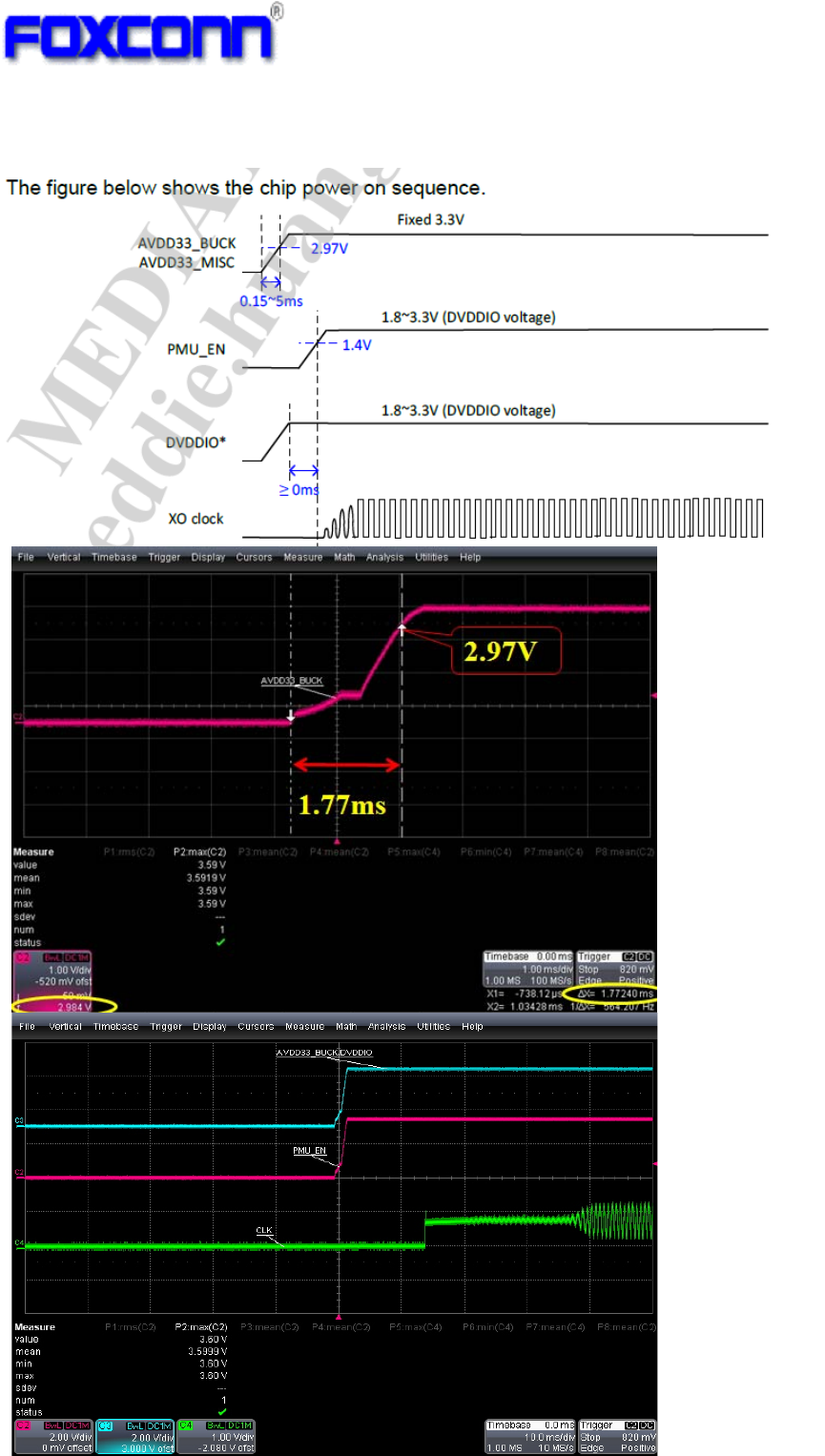
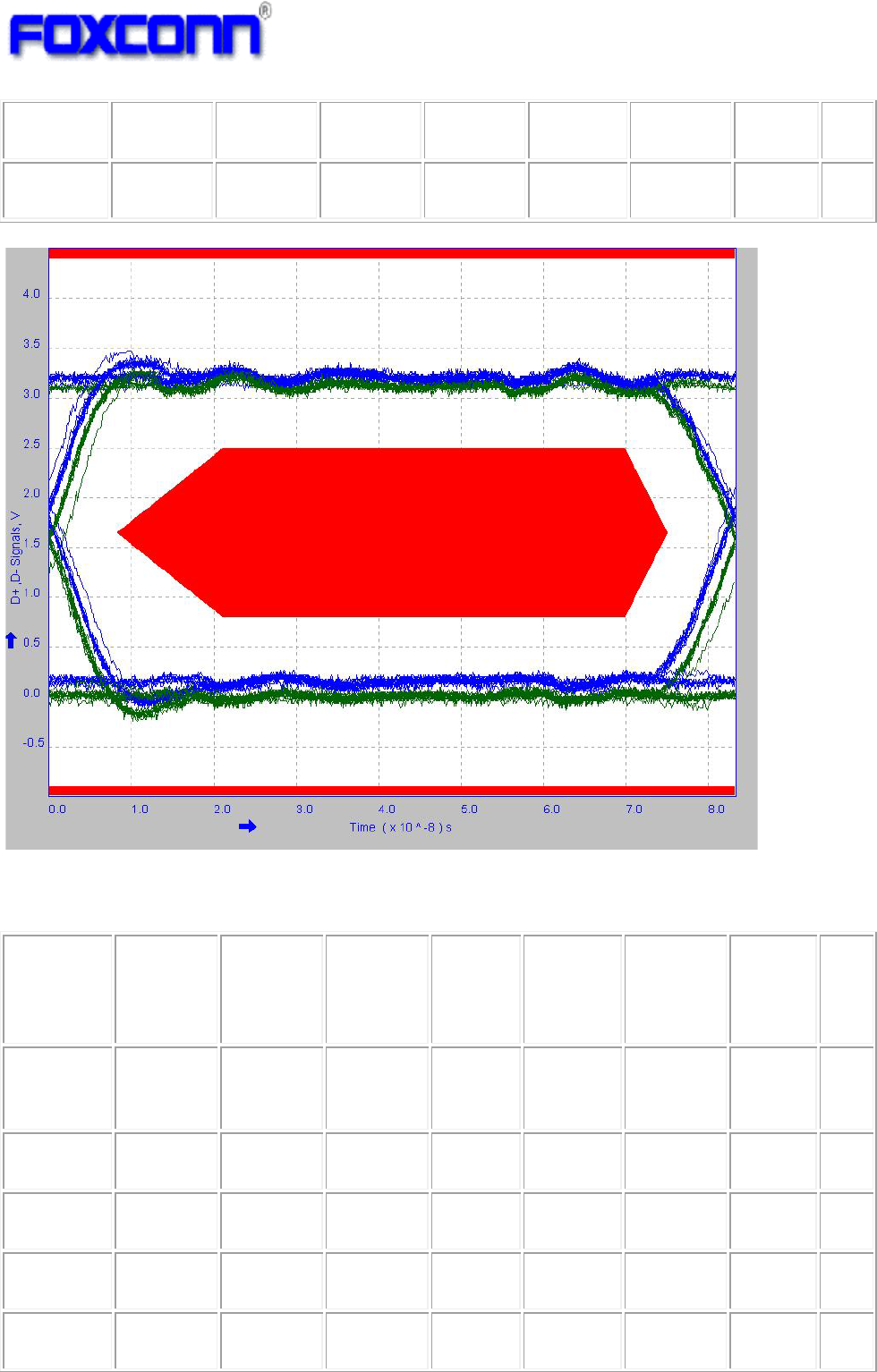
7.12 Power ON and power off sequence
7.12.1 Power on sequence
25
7.12.2 Power off sequence
TBD
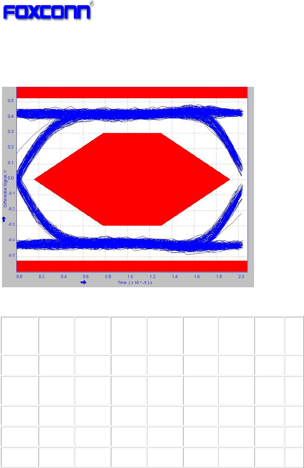
7.13 USB Eye Diagram
1)USB 2.0
Results based on USB-IF / Waiver Limits :
Measure
ment
Name
Minimu
m
Maximu
m Mean pk-pk
Standar
d
Deviatio
n
RMS Popula
tion
Stat
us
Monotonic
Property - - - - - - 0 Pass
Eye
Diagram
Test - - - - - - - Pass
Signal
Rate 472.8132
Mbps 486.6180
Mbps 480.0075
Mbps 0.0000bp
s 1.946978
Mbps 480.1003
Mbps 509 Pass
EOP Width - - 16.59637
ns - - - 1 Pass
EOP Width
(Bits) - - 7.966383 - - - 1 Pass
26
Falling
Edge Rate 1.131366
kV/us 1.475609
kV/us 1.311112
kV/us 344.2424
V/us 87.85163
V/us 1.314025
kV/us 108 Pass
Rising
Edge Rate 1.423693
V/us 1.511445
kV/us 1.256864
kV/us 1.510021
kV/us 143.8853
V/us 1.264998
kV/us 108 Pass
2)USB1.1
Results based on USB-IF / Waiver Limits :
Measure
ment
Name
Minimu
m
Maximu
m Mean pk-pk
Standar
d
Deviatio
n
RMS Popula
tion
Stat
us
Eye
Diagram
Test - - - - - - - Pass
Signal
Rate 11.82135
Mbps 12.20779
Mbps 12.00406
Mbps 0.0000b
ps 143.7864
kbps 12.01181
Mbps 28 Pass
Crossover
Voltage 1.635992
V 1.788064
V 1.713677
V 152.072
6mV 40.44978
mV 1.714130
V 19 Pass
EOP Width - - 165.8765
ns - - - 1 Pass
Consecutiv
e Jitter -838.4332
ps 652.0862
ps -133.4152
ps 1.49051
9ns 610.5417
ps 607.1521
ps 17 Pass
27
Paired JK
Jitter -419.5018
ps 301.5176
ps 5.597451
ps 721.019
5ps 242.5373
ps 221.4760
ps 6 Pass
Paired KJ
Jitter -408.5133
ps 331.1229
ps 0.0000s 739.636
2ps 250.7989
ps 234.6009
ps 8 Pass
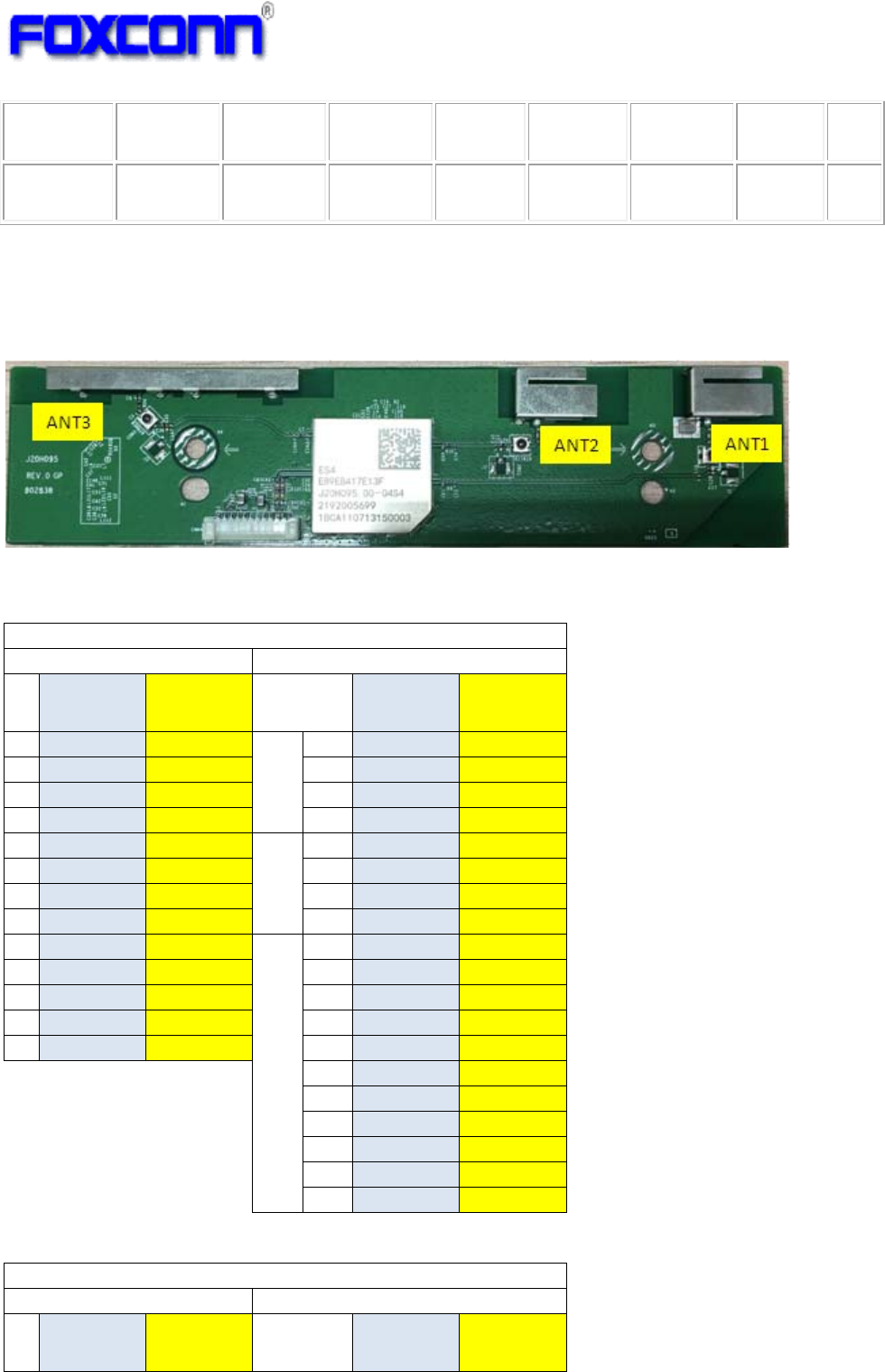
7.14 Antenna Electrical Specification
ANT1 (Free space)
Peak gain:
Wi-Fi ANT1
2.4GHz 5GHz
ch Freq
[MHz]
Peak Gain
[dBi] ch Freq
[MHz]
Peak Gain
[dBi]
1 2412 -2.69
W52
36 5180 -0.62
2 2417 -2.49 40 5200 -0.35
3 2422 -2.37 44 5220 0.33
4 2427 -2.25 48 5240 0.45
5 2432 -2.19
W53
52 5260 0.87
6 2437 -2.20 56 5280 1.14
7 2442 -2.08 60 5300 0.99
8 2447 -1.94 64 5320 0.69
9 2452 -1.81
W56
100 5500 0.33
10 2457 -1.72 104 5520 0.34
11 2462 -1.38 108 5540 0.27
12 2467 -1.10 112 5560 0.17
13 2472 -0.84 116 5580 -0.01
120 5600 -0.60
124 5620 -1.21
128 5640 -1.85
132 5660 -2.07
136 5680 -1.67
140 5700 -1.26
ANT2 (Free space)
Peak gain:
Wi-Fi ANT2
2.4GHz 5GHz
ch Freq
[MHz]
Peak Gain
[dBi] ch Freq
[MHz]
Peak Gain
[dBi]
ch Freq
[
MHz
]
Peak
G
ain
Freq
[
MHz
]
Peak
G
ain ch Freq
[
MHz
]
Peak
G
ain
Freq
[
MHz
]
Peak
G
ain ch Freq
[
MHz
]
Peak
G
ain ch Freq
[
MHz
]
Peak
G
ain ch Freq
[
MHz
]
Peak
G
ain
1 2412 0.96 36 5180 1.74 1 2412 -2.69 36 5180 -0.62 1 2402 4.23 28 2429
3
.80 55 2456
3
.22
2 2417 1.42 40 5200 2.06 2 2417 -2.49 40 5200 -0.35 2 2403 4.20 29 2430
3
.78 56 2457
3
.19
3 2422 1.70 44 5220 2.61 3 2422 -2.37 44 5220 0.33 3 2404 4.18 30 2431
3
.76 57 2458
3
.16
4 2427 2.12 48 5240
3
.21 4 2427 -2.25 48 5240 0.45 4 2405 4.17 31 2432
3
.73 58 2459
3
.11
5 2432 2.46 52 5260
3
.67 5 2432 -2.19 52 5260 0.87 5 2406 4.16 32 2433
3
.71 59 2460
3
.04
6 2437 2.64 56 5280
3
.67 6 2437 -2.20 56 5280 1.14 6 2407 4.16 33 2434
3
.69 60 2461 2.98
7 2442 2.99 60 5300
3
.32 7 2442 -2.08 60 5300 0.99 7 2408 4.15 34 2435
3
.67 61 2462 2.90
8 2447
3
.27 64 5320
3
.19 8 2447 -1.94 64 5320 0.69 8 2409 4.05 35 2436
3
.64 62 2463 2.83
9 2452
3
.35 100 5500 2.90 9 2452 -1.81 100 5500 0.33 9 2410 4.05 36 2437
3
.63 63 2464 2.77
10 2457
3
.63 104 5520
3
.23 10 2457 -1.72 104 5520 0.34 10 2411 4.08 37 2438
3
.61 64 2465 2.74
11 2462
3
.58 108 5540
3
.56 11 2462 -1.38 108 5540 0.27 11 2412 4.09 38 2439
3
.61 65 2466 2.72
12 2467
3
.72 112 5560
3
.56 12 2467 -1.10 112 5560 0.17 12 2413 4.11 39 2440
3
.61 66 2467 2.73
13 2472
3
.87 116 5580
3
.36 13 2472 -0.84 116 5580 -0.01 13 2414 4.11 40 2441
3
.61 67 2468 2.73
120 5600 2.99 120 5600 -0.60 14 2415 4.10 41 2442
3
.59 68 2469 2.72
124 5620 2.81 124 5620 -1.21 15 2416 4.07 42 2443
3
.58 69 2470 2.72
128 5640 2.67 128 5640 -1.85 16 2417 4.03 43 2444
3
.57 70 2471 2.69
132 5660 2.68 132 5660 -2.07 17 2418
3
.99 44 2445
3
.55 71 2472 2.65
136 5680 2.80 136 5680 -1.67 18 2419
3
.95 45 2446
3
.52 72 2473 2.61
140 5700 2.81 140 5700 -1.26 19 2420
3
.92 46 2447
3
.49 73 2474 2.55
149 5745 2.84 149 5745 -1.14 20 2421
3
.90 47 2448
3
.44 74 2475 2.49
153 5765 2.78 153 5765 -0.66 21 2422
3
.86 48 2449
3
.40 75 2476 2.43
157 5785
3
.04 157 5785 -0.44 22 2423
3
.82 49 2450
3
.35 76 2477 2.37
161 5805
3
.38 161 5805 -0.13 23 2424
3
.81 50 2451
3
.31 77 2478 2.38
165 5825
3
.25 165 5825 -0.64 24 2425
3
.80 51 2452
3
.29 78 2479 2.37
25 2426
3
.81 52 2453
3
.28 79 2480 2.37
26 2427
3
.82 53 2454
3
.26
27 2428
3
.81 54 2455
3
.24
W53
W56
ch
W58 W58
Bluetooth
Wi-Fi ANT2
2.4GHz帯 5GHz帯
W52
W53
W56
Wi-Fi ANT1
2.4GHz帯 5GHz帯
ch
W52
30
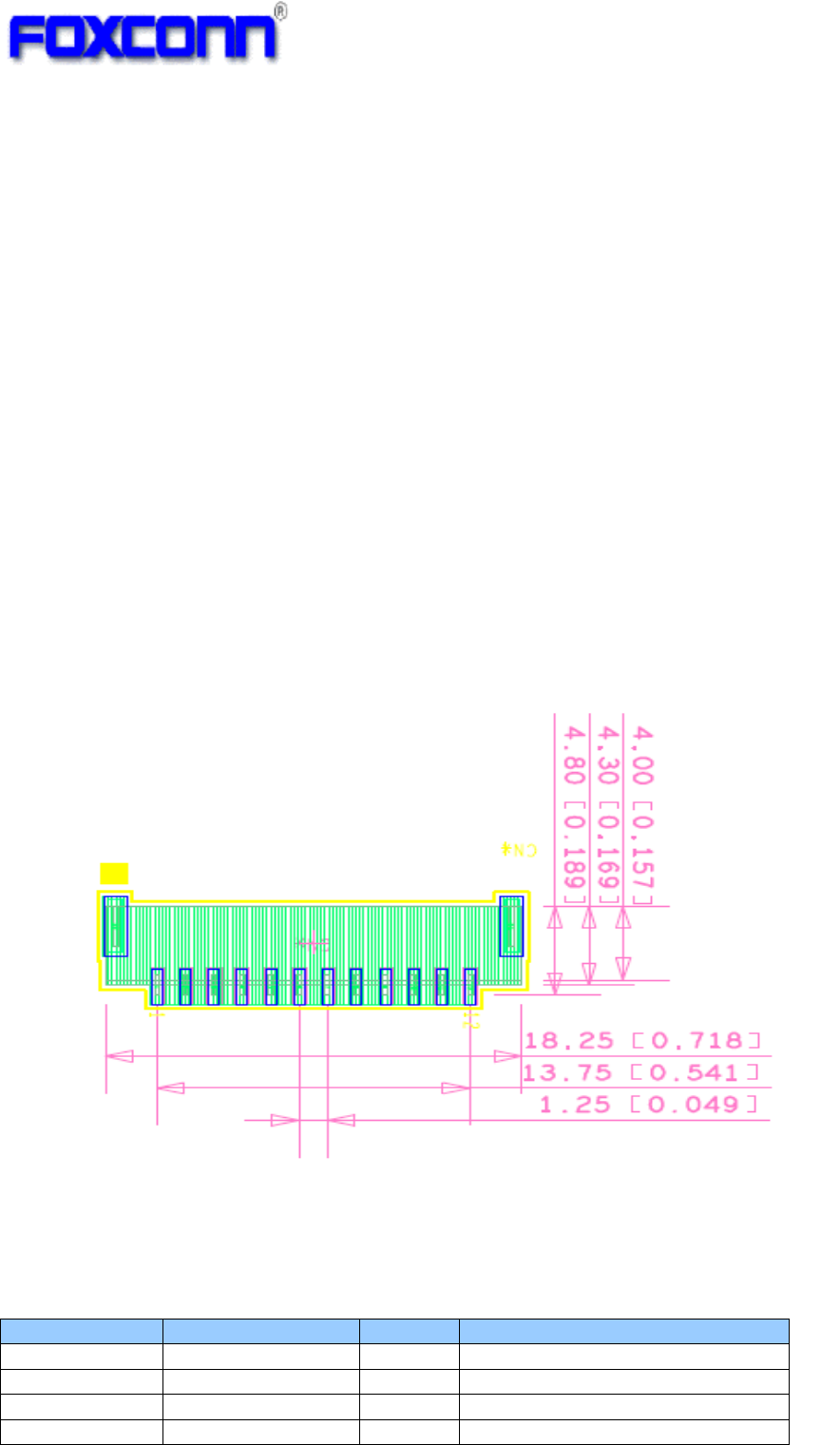
8 Mechanical Specifications
8.1 Shielding Cover Dimension
Dimension (LxWxH): 22.04mm x 27.26mm x 2.05mm
Thickness: 0.2mm
31
8.2 PCB Assembly Dimension
Dimension (W x Lx H ): 95mmx32mmx1.0mm
PCB: 4 layer FR4 design

32
8.3 Mount Position of Materials
All materials should be populated on a side.
Quantit
y Reference Vendor Vendor PN Description
11
R9,R10,R34,L111
,L112,C7,C20,C2
9,C34,R21,R61
Yageo RC0402JR-070RL
RES C SMD 0402 0ohm 5% GP/HF
TA-I RM04JTN0
WALSIN WR04X000 PTL
TA-I RM04JLN0
YAGEO RC0402JR-7D0RL
4 C24,C58,C60,C6
1
MURATA GRM155R71C104M
A88D
CAP CER 100nF 20% 16V SMD 0402 GP/HF
X7R 0.5mm
4 C2,C4,C67,C69
MURATA GJM1555C1HR30W
B01D
CAP CER 0.3pF +-0.05pF 50V SMD 0402 GP/HF
NPO T=0.5mm HI-Q
1 C16 MURATA GRM0335C1HR50B
A01D
CAP CER 0.5pF +-0.1pF 50V SMD 0201 GP/HF
NPO T=0.3mm
1 C53 MURATA LQP03TN0N8B02D IND TF 0.8nH 0.1nH 800mA 0.08ohm Q=14 SMD
0201 GP/HF
1 L22 MURATA GRM0335C1ER80B
A01D
CAP CER 0.8pF +-0.1pF 25V SMD 0201 GP/HF
NPO 0.3mm
1 C14 MURATA GJM0335C1ER90BB
01D
CAP CER 0.9pF +-0.1pF 25V SMD 0201 GP/HF
NPO 0.3mm HI-Q
1 L4 MURATA LQP03TN1N3B02D IND TF 1.3nH 0.1nH 600mA 0.15ohm Q=14 SMD
0201 GP/HF
1 L5 MURATA LQP03TN1N5B02D IND TF 1.5nH 0.1nH 600mA 0.15ohm Q=14 SMD
0201 GP/HF
1 C28 MURATA LQP03TG1N6B02D IND TF 1.6nH 0.1nH 600mA 0.15ohm Q=13 SMD
0201 GP/HF
2 C166,C167
MURATA GRM0335C1E101JA
01D
CAP CER 100pF 5% 25V SMD 0201 GP/HF NPO
T=0.3mm
2 R2,R32
YAGEO RC0201JR-0710KL
RES C SMD 0201 10Kohm 5% GP/HF 1/20W WALSIN WR02X103JAL
TA-I RM02JTN103
2 C18,C25
MURATA GRM033R70J103KA
01D CAP CER 10nF 10% 6.3V SMD 0201 GP/HF X7R
T=0.3mm
WALSIN 0201B103K6R3CT
YAGEO CC0201KRX7R5BB1
03
5 C37,C39,C41,C4
2,C128
MURATA GJM0336C1E100JB
01D
CAP CER 10pF 5% 25V SMD 0201 GP/HF C0H
T=0.3mm HI-Q
1 C26
MURATA GRM188C80G106M
E47D CAP CER 10uF 20% 4V SMD 0603 GP/HF X6S
0.8mm
SAMSUNG CL10X106MR8NNN
C
1 C55 MURATA LQP03TN1N0B02D IND TF 1.0nH 0.1nH 750mA 0.1ohm Q=14 SMD
0201 GP/HF
2 C21,C22
TA-I RM02JTN0
RES C SMD 0201 0ohm 5% GP/HF 1/20W YAGEO RC0201JR-070RL
WALSIN WR02X000 PAL
2 L7,L8 MURATA GJM0335C1ER20W
B01D
CAP CER 0.2pF +-0.05pF 25V SMD 0201 GP/HF
NPO T=0.3mm HI-Q
7 C27,C31,C32,C4
6,C47,C51,C52
MURATA GRM155C80J105KE
15D CAP CER 1uF 10% 6.3V SMD 0402 GP/HF X6S
0.5mm
TAIYO JMK105C6105KV-F
1 C62 MURATA LQP03TN2N2B02D IND TF 2.2nH 0.1nH 600mA 0.15ohm Q=14 SMD
0201 GP/HF
3 C45,C70,C71
SAMSUNG CL10B225KP8NNNC CAP CER 2.2uF 10% 10V SMD 0603 GP/HF X7R
T=0.8mm
MURATA GRM188R71A225KE

33
15D
TAIYO LMK107B7225KA-TR
1 L10 TAIYO NR3015T2R2M IND WW 2.2uH 20% 1.5A 0.06ohm SMD GP/HF
1 C15 MURATA LQP03TN2N7B02D IND TF 2.7nH 0.1nH 500mA 0.2ohm Q=14 SMD
0201 GP/HF
1 L21 MURATA LQP03TN3N9B02D IND TF 3.9nH 0.1nH 400mA 0.3ohm Q=14 SMD
0201 GP/HF
2 C30,C165 MURATA GRM188C71A475KE
11D
CAP CER 4.7uF 10% 10V SMD 0603 GP X7S
T=0.8mm
2 C63,C64
MURATA GRM21BR60J476ME
15L CAP CER 47uF 20% 6.3V SMD 0805 GP/HF X5R
1.25mm
TAIYO JMK212BJ476MG-T
SAMSUNG CL21A476MQYNNN
E
1 R31 Murata
GJM1555C1H2R2BB
01D
CAP CER 2.2pF +-0.1pF 50V SMD 0402 GP/HF
NPO T=0.5mm HI-Q
1 R33 MURATA
GJM1555C1H4R7BB
01D
CAP CER 4.7pF +-0.1pF 50V SMD 0402 GP/HF
NPO T=0.5mm HI-Q
1 C1 Murata LQG15HS3N0B02
IND C 3.0nH 0.1nH 800mA 0.125ohm Q=8 SMD
0402 GP/HF
1 C3 Murata LQG15HS1N6B02
IND C 1.6nH 0.1NH 1000mA 0.07ohm Q=8 SMD
0402 GP/HF
2 C84,C85 MURATA
GRM1555C1H6R8C
A01D
CAP CER 6.8pF +-0.25pF 50V SMD 0402 GP/HF
NPO T=0.5mm
1 U7 TXC 7M40000127 XTAL 40MHz 10PPM 12pF 20ohm SMD GP
3.2*2.5MM -10~+95DegC
Hosonic E3SB40E00010DE
2 U2,U3 ACX
DP1608-A2455DTA2
T/LF
FILTER DIPLEXER 2400~2500/4900~5950MHz
0.75/1.1dB SMD 0603 GP/HF
3 CON1,CON2,CO
N3 MURATA MM8430-2610RA1 HEADER RF 1*1PORT D=0.6mm SMD FEMALE
ST GP/HF
1 CON4 J.A.M. STA12-12WH-ET
CONN WTB 12PIN 1.25mm SMD FEMALE RT
GP
1 U6 MEDIATEK MT7668BUN IC PER 3.3V SMD QFN76 GP/HF
WI-FI/BLUETOOTH MT7668BUN
1 ANT1/WiFi1 Foxconn
ANTSR02-CSGTB-E
F
BRACKET 15.3*9.8*5.3mm T=0.3mm REV.X4
J20H095.00 C7701 GP
1 ANT2/WiFi2 Foxconn
ANTSR02-CSGTC-E
F
BRACKET 15.3*9.8*5.3mm T=0.3mm REV.X4
J20H095.00 C7701 GP
1 ANT3/BT Foxconn
ANTSR01-CSGTA-E
F
BRACKET 53*4.6*5.3mm T=0.3mm REV.X4
J20H095.00 C7701 GP
1 PCB APCB 308.02838.025 EU-GP PCB 4L OSP REV.025 10PCS GP/HF
150*35
ZDT
1 SC1 FOXCONN 426.04947.005
SHIELD COVER 23.09*22.40*2.05mm REV.0
J20H095.00 C7521 T=0.2mm GP
0.1 Label LABEL BLANK 19.05*5mm REV.1 WHITE GP/HF
T77H470.00
0.3 solder SOLDER PASTE S3X58 M500 GP/HF
J20H095.00-Bottom layer (Top view):

34
35
9 PCB Specification
PCB Stack-up:
PCB Thickness:1.0mm+/-10%
PCB Layers:4 Layers
Material: FR-4 Middle Tg:140 (Min135)
LayerTypicallayerthickness(mm)Typicallayerthickness(mil)
L10.035 1.3780
0.170 6.6929
L20.035 1.3780
0.520 20.4724
L30.035 1.3780
0.170 6.6929
L40.035 1.3780
J20H095.00 (PCB color: Green)
36
Transmission Line:
RF Line (50ohm)
USB T/R Line (90ohm)

37
12 OTP content
User Area (0x138~0X13F)
Index Description Value Efuse
Location content
ZZ Serial Number
(High)
It starts from 1 in each line every morning.
It will be incremented by one.
Ex. Serial Number = 32 (Decade)
0xZZ=0x00, 0xZZ=0x20,range:0001-FFFF
0x138 TBD
ZZ Serial Number (Low) 0x139 TBD
YY Year Year (0x11=>2017,0x12=>2018,0x13=>2019) 0x13A 11
MM Month Month (range : 0x01-0x0C) 0x13B 07
DD Date Date (range : 0x01-0x1F) 0x13C TBD
LL Line Number Line Number (range : 0x01 -0xFF) 0x13D TBD
N Module Identification Print “0” 0x13E 00
C Region code Print “0”
HH Hardware Version 2
Trial and Revision Number for TV Module
0x13F 04
00=ES1 01=ES2 02=ES3 03=ES4 04=MVT
05=MP 06~0FF=Reserved
Efuse Map
Offset Description value value Type
0x00 Chip ID 68 Defined in BIN
0x01 76 Defined in BIN
0x02 E-fuse Version 00 Defined in BIN
0x03 00 Defined in BIN
0x04 1st WLAN Mac Address [7:0] match with laser making
0x05 1st WLAN Mac Address [15:8] match with laser making
0x06 1st WLAN Mac Address [23:16] match with laser making
0x07 1st WLAN Mac Address [31:24] match with laser making
0x08 1st WLAN Mac Address [39:32] match with laser making
0x09 1st WLAN Mac Address [47:40] match with laser making
0x0A Reserved 68 Defined in BIN
0x0B Reserved 76 Defined in BIN
0x0C Reserved C3 Defined in BIN
0x0D Reserved 14 Defined in BIN
0x0E Reserved 00 Defined in BIN
0x0F Reserved 00 Defined in BIN
0x10 Reserved 80 Defined in BIN
0x11 Reserved 02 Defined in BIN
0x12 Reserved C3 Defined in BIN
0x13 Reserved 14 Defined in BIN
0x14 Reserved 15 Defined in BIN
0x15 Reserved 76 Defined in BIN
0x16 Reserved 03 Defined in BIN
0x17 Reserved 22 Defined in BIN
0x18 Reserved FF Defined in BIN
0x19 Reserved FF Defined in BIN
0x1A Reserved 23 Defined in BIN

38
0x1B Reserved 04 Defined in BIN
0x1C Reserved 0D Defined in BIN
0x1D Reserved F2 Defined in BIN
0x1E Reserved 8F Defined in BIN
0x1F Reserved 02 Defined in BIN
0x20 Reserved 00 Defined in BIN
0x21 Reserved 80 Defined in BIN
0x22 Reserved 0A Defined in BIN
0x23 Reserved 20 Defined in BIN
0x24 Reserved 00 Defined in BIN
0x25 Reserved 02 Defined in BIN
0x26 Reserved 00 Defined in BIN
0x27 Reserved 00 Defined in BIN
0x28 Reserved 00 Defined in BIN
0x29 Reserved 00 Defined in BIN
0x2A Reserved 00 Defined in BIN
0x2B Reserved 00 Defined in BIN
0x2C Reserved 00 Defined in BIN
0x2D Reserved 00 Defined in BIN
0x2E Reserved 00 Defined in BIN
0x2F Reserved 00 Defined in BIN
0x30 HW configuration-0 option (Cfg0_opt) 00 Defined in BIN
0x31 00 Defined in BIN
0x32 HW configuration-1 option (Cfg1_opt) 20 Defined in BIN
0x33 A0 Defined in BIN
0x34 NIC Configure 0 22 Defined in BIN
0x35 00 Defined in BIN
0x36 NIC Configure 1 04 Defined in BIN
0x37 60 Defined in BIN
0x38 Reserved 83 Defined in BIN
0x39 00 Defined in BIN
0x3A TX BBP Configuration 20 Defined in BIN
0x3B LED MODE 00 Defined in BIN
0x3C ePA/eLNA control polarity 00 Defined in BIN
0x3D Reserved 00 Defined in BIN
0x3E ePA/eLNA Antenna control 00 Defined in BIN
0x3F Reserved 00 Defined in BIN
0x40 Reserved 00 Defined in BIN
0x41 Reserved 00 Defined in BIN
0x42 NIC Configure 2 22 Defined in BIN
0x43 NIC Configure 3 00 Defined in BIN
0x44 Reserved 00 Defined in BIN
0x45 Reserved 00 Defined in BIN
0x46
Reserved
00 Defined in BIN
0x47 00 Defined in BIN
0x48 00 Defined in BIN
0x49 00 Defined in BIN
0x4A Reserved 00 Defined in BIN

39
0x4B Reserved 00 Defined in BIN
0x4C Reserved 00 Defined in BIN
0x4D Reserved 00 Defined in BIN
0x4E Reserved 00 Defined in BIN
0x4F Reserved 00 Defined in BIN
0x50 COEX isolation index 00 Defined in BIN
0x51 Reserved 00 Defined in BIN
0x52 Reserved 00 Defined in BIN
0x53 Reserved IC
0x54 Reserved IC
0x55 Temperature sensor calibration IC
0x56 TX0 2.4G PA TSSI slope 42 Defined in BIN
0x57 TX0 2.4G PA TSSI offset C2 Defined in BIN
0x58 TX0 2.4G TX power (54Mbps, dBm absolute value) 1C Defined in BIN
0x59 TX0 2.4G TX power offset low group (CH1~5)
(delta, dB) Write in FT
0x5A TX0 2.4G TX power offset middle group (CH6~10)
(delta, dB) Write in FT
0x5B TX0 2.4G TX power offset high group (CH11~14)
(delta, dB) Write in FT
0x5C TX1 2.4G PA TSSI slope C2 Defined in BIN
0x5D TX1 2.4G PA TSSI offset C4 Defined in BIN
0x5E TX1 2.4G TX power (54Mbps,dBm, absolute value) 1C Defined in BIN
0x5F TX1 2.4G TX power offset low group (CH1~5)
(delta, dB) Write in FT
0x60 TX1 2.4G TX power offset middle group (CH6~10)
(delta, dB) Write in FT
0x61 TX1 2.4G TX power offset high group (CH11~14)
(delta, dB) Write in FT
0x62 ~ 0x68 Reserved 00 Defined in BIN
0x69 Reserved 08 Defined in BIN
0x6A~0x6D Reserved 00 Defined in BIN
0x6E TX0 5G PA TSSI slope Group0: 4910 ~ 5140MHz
(CH184, 188, 192, 196, 8, 12, 16) B9 Defined in BIN
0x6F TX0 5G PA TSSI offset Group0: 4910 ~ 5140MHz
(CH184, 188, 192, 196, 8, 12, 16) C6 Defined in BIN
0x70
TX0 5G Target power of Group0: 4910 ~ 5140MHz
(54M,dBm,Abs-value)(CH184, 188, 192, 196, 8,
12, 16)
18 Defined in BIN
0x71 TX0 5G TX power offset low Group0: 4910 ~
4970MHz (delta, dB) (CH184, 188, 192) Write in FT
0x72 TX0 5G TX power offset high Group0: 4970 ~
5140MHz (delta, dB) (CH196, 8, 12, 16) Write in FT
0x73 TX0 5G PA TSSI slope Group1: 5140 ~ 5250MHz
(CH36, 40, 44, 48) B9 Defined in BIN
0x74 TX0 5G PA TSSI offset Group1: 5140 ~ 5250MHz
(CH36, 40, 44, 48) C6 Defined in BIN
0x75 TX0 5G Target power of Group1: 5140 ~ 5250MHz
(54M,dBm, Abs-value)(CH36, 40, 44, 48) 18 Defined in BIN
0x76 TX0 5G TX power offset low Group1: 5140 ~
5210MHz (delta,dB)(CH36,40) Write in FT

40
0x77 TX0 5G TX power offset high Group1: 5210 ~
5250MHz (delta, dB) (CH44, 48) Write in FT
0x78 TX0 5G PA TSSI slope Group2: 5250 ~ 5360MHz
(CH52, 56, 60, 64) B9 Defined in BIN
0x79 TX0 5G PA TSSI offset Group2: 5250 ~ 5360MHz
(CH52, 56, 60, 64) C6 Defined in BIN
0x7A TX0 5G Target power of Group2: 5250 ~ 5360MHz
(54M,dBm, Abs-value) CH52, 56, 60, 64) 18 Defined in BIN
0x7B TX0 5G TX power offset low Group2: 5250 ~
5290MHz (delta, dB) (CH52, 56) Write in FT
0x7C TX0 5G TX power offset high Group2: 5290 ~
5360MHz (delta, dB) (CH60, 64) Write in FT
0x7D TX0 5G PA TSSI slope Group3:5360 ~ 5470MHz
(Reserved) 39 Defined in BIN
0x7E TX0 5G PA TSSI offset Group3: 5360 ~
5470MHz(Reserved) C5 Defined in BIN
0x7F TX0 5G Target power of Group3: 5360 ~ 5490MHz
(54M,dBm, Abs-value) (Reserved) 18 Defined in BIN
0x80 TX0 5G TX power offset low Group3: 5360 ~
5430MHz (delta, dB) (Reserved) Write in FT
0x81 TX0 5G TX power offset high Group3 : 5430 ~
5470MHz (delta, dB) (Reserved) Write in FT
0x82 TX0 5G PA TSSI slope Group4: 5470 ~ 5580MHz
(CH100, 104, 108, 112, 116) 39 Defined in BIN
0x83 TX0 5G PA TSSI offset Group4: 5470 ~ 5580MHz
(CH100, 104, 108, 112, 116) C5 Defined in BIN
0x84
TX0 5G Target power of Group4: 5470 ~ 5580MHz
(54M,dBm, Abs-value) (CH100, 104, 108, 112,
116)
18 Defined in BIN
0x85 TX0 5G TX power offset low Group4: 5470 ~
5530MHz (delta, dB) (CH100, 104) Write in FT
0x86 TX0 5G TX power offset high Group4: 5530 ~
5580MHz (delta, dB) (CH108, 112, 116) Write in FT
0x87 TX0 5G PA TSSI slope Group5: 5580 ~ 5690MHz
(CH120, 124, 128, 132, 136) 39 Defined in BIN
0x88 TX0 5G PA TSSI offset Group5: 5580 ~ 5690MHz
(CH120, 124, 128, 132, 136) C4 Defined in BIN
0x89
TX0 5G Target power of Group5: 5580 ~ 5690MHz
(54M,dBm, Abs-value) (CH120, 124, 128, 132,
136)
18 Defined in BIN
0x8A TX0 5G TX power offset low Group5: 5580 ~
5690MHz (delta, dB) (CH120, 124) Write in FT
0x8B TX0 5G TX power offset high Group5: 5580 ~
5690MHz (delta, dB) (CH128, 132, 136) Write in FT
0x8C TX0 5G PA TSSI slope Group6: 5690 ~ 5800MHz
(CH140, 144, 149, 153, 157) B9 Defined in BIN
0x8D TX0 5G PA TSSI offset Group6: 5690 ~ 5800MHz
(CH140, 144, 149, 153, 157) C3 Defined in BIN
0x8E TX0 5G Target power of Group6: 5690 ~ 5800MHz
(54M,dBm, Abs-value)(CH140, 144, 149, 153, 157) 18 Defined in BIN
0x8F TX0 5G TX power offset low Group6: 5690 ~
5730MHz (delta, dB) (CH4140, CH144) Write in FT

41
0x90 TX0 5G TX power offset high Group6: 5730 ~
5800MHz (delta, dB) (CH4149, 153, 157) Write in FT
0x91 TX0 5G PA TSSI slope Group7: 5800 ~ 5925MHz
(CH161, 165) 39 Defined in BIN
0x92 TX0 5G PA TSSI offset Group7: 5800 ~ 5925MHz
(CH161, 165) C3 Defined in BIN
0x93 TX0 5G Target power of Group7: 5800 ~ 5925MHz
(54M,dBm, Abs-value) (CH161, 165) 18 Defined in BIN
0x94 TX0 5G TX power offset low Group7: 5800 ~5815
(delta, dB) (CH161) Write in FT
0x95 TX0 5G TX power offset high Group7: 5815 ~5925
(delta, dB) (CH165) Write in FT
0x96 TX1 5G PA TSSI slope Group0: 4910 ~ 5140MHz
(CH184, 188, 192, 196, 8, 12, 16) B9 Defined in BIN
0x97 TX1 5G PA TSSI offset Group0: 4910 ~ 5140MHz
(CH184, 188, 192, 196, 8, 12, 16) C5 Defined in BIN
0x98
TX1 5G Target power of Group0: 4910 ~ 5140MHz
(54M,dBm,Abs-value)(CH184, 188, 192, 196, 8,
12, 16)
18 Defined in BIN
0x99 TX1 5G TX power offset low Group0: 4910 ~
4970MHz (delta, dB) (CH184, 188, 192) Write in FT
0x9A TX1 5G TX power offset high Group0: 4970 ~
5140MHz (delta, dB) (CH196, 8, 12, 16) Write in FT
0x9B TX1 5G PA TSSI slope Group1: 5140 ~ 5250MHz
(CH36, 40, 44, 48) 39 Defined in BIN
0x9C TX1 5G PA TSSI offset Group1: 5140 ~ 5250MHz
(CH36, 40, 44, 48) C5 Defined in BIN
0x9D TX1 5G Target power of Group1: 5140 ~ 5250MHz
(54M,dBm, Abs-value)(CH36, 40, 44, 48) 18 Defined in BIN
0x9E TX1 5G TX power offset low Group1: 5140 ~
5210MHz (delta,dB)(CH36,40) Write in FT
0x9F TX1 5G TX power offset high Group1: 5210 ~
5250MHz (delta, dB) (CH44, 48) Write in FT
0xA0 TX1 5G PA TSSI slope Group2: 5250 ~ 5360MHz
(CH52, 56, 60, 64) B9 Defined in BIN
0xA1 TX1 5G PA TSSI offset Group2: 5250 ~ 5360MHz
(CH52, 56, 60, 64) C4 Defined in BIN
0xA2 TX1 5G Target power of Group2: 5250 ~ 5360MHz
(54M,dBm, Abs-value) (CH52, 56, 60, 64) 18 Defined in BIN
0xA3 TX1 5G TX power offset low Group2: 5250 ~
5290MHz (delta, dB) (CH52, 56) Write in FT
0xA4 TX1 5G TX power offset high Group2: 5290 ~
5360MHz (delta, dB) (CH60, 64) Write in FT
0xA5 TX1 5G PA TSSI slope Group3:5360 ~ 5470MHz
(Reserved) 39 Defined in BIN
0xA6 TX1 5G PA TSSI offset Group3: 5360 ~ 5470MHz
(Reserved) C4 Defined in BIN
0xA7 TX1 5G Target power of Group3: 5360 ~ 5490MHz
(54M,dBm, Abs-value) (Reserved) 18 Defined in BIN
0xA8 TX1 5G TX power offset low Group3: 5360 ~
5430MHz (delta, dB) (Reserved) Write in FT
0xA9 TX1 5G TX power offset high Group3 : 5430 ~
5470MHz (delta, dB) (Reserved) Write in FT

42
0xAA TX1 5G PA TSSI slope Group4: 5470 ~
5580MHz(CH100, 104, 108, 112, 116) B9 Defined in BIN
0xAB TX1 5G PA TSSI offset Group4: 5470 ~
5580MHz(CH100, 104, 108, 112, 116) C3 Defined in BIN
0xAC
TX1 5G Target power of Group4: 5470 ~
5580MHz(5490MHz (54M,dBm, Abs-value)
(CH100, 104, 108, 112, 116)
18 Defined in BIN
0xAD TX1 5G TX power offset low Group4: 5470 ~
5530MHz (delta, dB) (CH100, 104) Write in FT
0xAE TX1 5G TX power offset high Group4: 5530 ~
5580MHz (delta, dB) (CH108, 112, 116) Write in FT
0xAF TX1 5G PA TSSI slope Group5: 5580 ~ 5690MHz
(CH120, 124, 128, 132, 136) 39 Defined in BIN
0xB0 TX1 5G PA TSSI offset Group5: 5580 ~ 5690MHz
(CH120, 124, 128, 132, 136) C3 Defined in BIN
0xB1
TX1 5G Target power of Group5: 5580 ~ 5690MHz
(54M,dBm, Abs-value) (CH120, 124, 128, 132,
136)
18 Defined in BIN
0xB2 TX1 5G TX power offset low Group5: 5580 ~
5690MHz (delta, dB) (CH120, 124) Write in FT
0xB3 TX1 5G TX power offset high Group5: 5580 ~
5690MHz (delta, dB) (CH128, 132, 136) Write in FT
0xB4 TX1 5G PA TSSI slope Group6: 5690 ~ 5800MHz
(CH140, 144, 149, 153, 157) 39 Defined in BIN
0xB5 TX1 5G PA TSSI offset Group6: 5690 ~ 5800MHz
(CH140, 144, 149, 153, 157) C3 Defined in BIN
0xB6
TX1 5G Target power of Group6: 5690 ~ 5800MHz
(54M,dBm, Abs-value) (CH140, 144, 149, 153,
157)
18 Defined in BIN
0xB7 TX1 5G TX power offset low Group6: 5690 ~
5730MHz (delta, dB) (CH4140, CH144) Write in FT
0xB8 TX1 5G TX power offset high Group6: 5730 ~
5800MHz (delta, dB) (CH4149, 153, 157) Write in FT
0xB9 TX1 5G PA TSSI slope Group7: 5800 ~ 59250MHz
(CH161, 165) B9 Defined in BIN
0xBA TX1 5G PA TSSI offset Group7: 5800 ~ 59250MHz
(CH161, 165) C2 Defined in BIN
0xBB TX1 5G Target power of Group7: 5800 ~
59250MHz (54M,dBm, Abs-value) (CH161, 165) 18 Defined in BIN
0xBC TX1 5G TX power offset low Group7: 5800 ~5815
(delta, dB) (CH161) Write in FT
0xBD TX1 5G TX power offset high Group7: 5815 ~5925
(delta, dB) (CH165) Write in FT
0xBE 2.4GHz TX power for CCK 1M/2M (delta, dB) C4 Defined in BIN
0xBF 2.4GHz TX power for CCK 5.5M/11M (delta, dB) C4 Defined in BIN
0xC0 2.4GHz TX power for OFDM 6M/9M (delta, dB) C2 Defined in BIN
0xC1 2.4GHz TX power for OFDM 12M/18M (delta, dB) C2 Defined in BIN
0xC2 2.4GHz TX power for OFDM 24M/36M (delta, dB) 00 Defined in BIN
0xC3 2.4GHz TX power for OFDM 48M (delta, dB) 00 Defined in BIN
0xC4 2.4GHz TX power for OFDM 54M (delta, dB) 00 Defined in BIN
0xC5 2.4G TX power for HT20 MCS=0(delta, dB) C2 Defined in BIN
2.4G TX power for VHT20 MCS=0(delta, dB)

43
0xC6 2.4G TX power for HT40 MCS=32(delta, dB) C2 Defined in BIN
0xC7 2.4G TX power for HT20 MCS=1,2(delta, dB) C2 Defined in BIN
2.4G TX power for VHT20 MCS=1,2(delta, dB)
0xC8 2.4G TX power for HT20 MCS=3,4(delta, dB) C2 Defined in BIN
2.4G TX power for VHT20 MCS=3,4(delta, dB)
0xC9 2.4G TX power for HT20 MCS=5(delta, dB) 00 Defined in BIN
2.4G TX power for VHT20 MCS=5(delta, dB)
0xCA 2.4G TX power for HT20 MCS=6(delta, dB) 00 Defined in BIN
2.4G TX power for VHT20 MCS=6(delta, dB)
0xCB 2.4G TX power for HT20 MCS=7(delta, dB) 00 Defined in BIN
2.4G TX power for VHT20 MCS=7(delta, dB)
0xCC 2.4G TX power for VHT20 MCS=8(delta, dB) 82 Defined in BIN
0xCD 2.4G TX power for HT40 MCS=0(delta, dB) 00 Defined in BIN
0xCE 2.4G TX power for HT40 MCS=1, 2(delta, dB) 00 Defined in BIN
0xCF 2.4G TX power for HT40 MCS=3, 4(delta, dB) 00 Defined in BIN
0xD0 2.4G TX power for HT40 MCS=5(delta, dB) 00 Defined in BIN
0xD1 2.4G TX power for HT40 MCS=6(delta, dB) 00 Defined in BIN
0xD2 2.4G TX power for HT40 MCS=7(delta, dB) 00 Defined in BIN
0xD3 2.4G TX power delta for VHT40 (delta, dB)
reference point VHT20 00 Defined in BIN
0xD4 2.4G TX power delta for LG VHT40 duplicate mode
(delta, dB) 00 Defined in BIN
0xD5 5G TX power for OFDM6M/9M (delta, dB) C2 Defined in BIN
0xD6 5G TX power for OFDM12M/18M (delta, dB) C2 Defined in BIN
0xD7 5G TX power for OFDM24M/36M (delta, dB) 00 Defined in BIN
0xD8 5G TX power for OFDM48M (delta, dB) 00 Defined in BIN
0xD9 5G TX power for OFDM54M (delta, dB) 00 Defined in BIN
0xDA 5G TX power for HT20 MCS=0(delta, dB) C2 Defined in BIN
5G TX power for VHT20 MCS=0(delta, dB)
0xDB 5G TX power for HT40 MCS=32(delta, dB) C2 Defined in BIN
0xDC 5G TX power for HT20 MCS=1, 2/9,10(delta, dB) C2 Defined in BIN
5G TX power for VHT20 MCS=0(delta, dB)
0xDD 5G TX power for HT20 MCS=3, 4/11, 12(delta, dB) C2 Defined in BIN
5G TX power for VHT20 MCS=3, 4(delta, dB)
0xDE 5G TX power for HT20 MCS=5/13, dB) 00 Defined in BIN
5G TX power for VHT20 MCS=5(delta, dB)
0xDF 5G TX power for HT20 MCS=6/14(delta, dB) 00 Defined in BIN
5G TX power for VHT20 MCS=6(delta, dB)
0xE0 5G TX power for HT20 MCS=7/15(delta, dB) 00 Defined in BIN
5G TX power for VHT20 MCS=7(delta, dB)
0xE1 5G TX power for VHT20 MCS=8(delta, dB) 82 Defined in BIN
0xE2 5G TX power for VHT20 MCS=9(delta, dB) 82 Defined in BIN
0xE3 5G TX power for HT40 MCS=0(delta, dB) C2 Defined in BIN
0xE4 5G TX power for HT40 MCS=1,2/9,10 (delta, dB) C2 Defined in BIN
0xE5 5G TX power for HT40 MCS=3,4/11,12 (delta, dB) C2 Defined in BIN
0xE6 5G TX power for HT40 MCS=5/13 (delta, dB) 00 Defined in BIN
0xE7 5G TX power for HT40 MCS=6/14 (delta, dB) 00 Defined in BIN
0xE8 5G TX power for HT40 MCS=7/15 (delta, dB) 00 Defined in BIN
0xE9 5G TX VHT40 power (delta, dB) referring to VHT20 00 Defined in BIN

44
0xEA 5G TX VHT80 power (delta, dB) referring to VHT20 00 Defined in BIN
0xEB 5G TX VHT80+80 power (delta, dB) referring to
VHT20 00 Defined in BIN
0xEC Reserved 00 Defined in BIN
0xED Reserved 00 Defined in BIN
0xEE 2.4G TX power for VHT20 MCS9 (delta, dB) 82 Defined in BIN
0xEF Reserved 22 Defined in BIN
0xF0 Reserved 22 Defined in BIN
0xF1 Reserved IC
0xF2 Reserved 00 Defined in BIN
0xF3 Reserved 00 Defined in BIN
0xF4 Frequency offset (XTAL calibration) Write in FT
0xF5 XTAL trim compensation 00 Defined in BIN
0xF6 Reserved 00 Defined in BIN
0xF7 Reserved IC
0xF8 Reserved 00 Defined in BIN
0xF9 ~ 0xFD Reserved 00 Defined in BIN
0xFE Reserved 00 Defined in BIN
0xFF Reserved 40 Defined in BIN
0x100 ~ 0x12B Reserved 00 Defined in BIN
0x12C iPA/ePA 2.4GHz band FE(Front End) loss between
Ant and Chip port 02 Defined in BIN
0x12D iPA/ePA 5GHz band FE(Front End) loss between
Ant and Chip port 03 Defined in BIN
0x12E ~ 0x137 Reserved 00 Defined in BIN
0x138~0x13F Reserved for Customer Specific Request match with laser making
0x140 ~ 0x14F Reserved 00 Defined in BIN
0x150 Reserved 06 Defined in BIN
0x151 Reserved 10 Defined in BIN
0x152 Reserved 00 Defined in BIN
0x153 Reserved 00 Defined in BIN
0x154 Reserved 08 Defined in BIN
0x155 Reserved 00 Defined in BIN
0x156 Reserved E0 Defined in BIN
0x157 Reserved 01 Defined in BIN
0x158 bcdUSB 00 Defined in BIN
0x159 00 Defined in BIN
0x15A idVendor 8D Defined in BIN
0x15B 0E Defined in BIN
0x15C idProduct 68 Defined in BIN
0x15D 76 Defined in BIN
0x15E bcdDevice 00 Defined in BIN
0x15F 00 Defined in BIN
0x160 ~ 0x177 Reserved 00 Defined in BIN
0x178 Reserved IC
0x179 Reserved IC
0x17A Reserved IC
0x17B Reserved IC
0x17C ~ 0x18E Reserved 00 Defined in BIN

45
0x18F Reserved CA Defined in BIN
0x190 Reserved CE Defined in BIN
0x191 Reserved CE Defined in BIN
0x192 Reserved CE Defined in BIN
0x193 Reserved CD Defined in BIN
0x194 Reserved CE Defined in BIN
0x195 Reserved CE Defined in BIN
0x196 Reserved CE Defined in BIN
0x197 Reserved CE Defined in BIN
0x198 Reserved D4 Defined in BIN
0x199 Reserved D0 Defined in BIN
0x19A Reserved D0 Defined in BIN
0x19B Reserved D0 Defined in BIN
0x19C Reserved CF Defined in BIN
0x19D Reserved D0 Defined in BIN
0x19E Reserved D0 Defined in BIN
0x19F Reserved CF Defined in BIN
0x1A0 Reserved D0 Defined in BIN
0x1A1 Reserved CA Defined in BIN
0x1A2 Reserved CE Defined in BIN
0x1A3 Reserved CD Defined in BIN
0x1A4 Reserved CD Defined in BIN
0x1A5 Reserved CE Defined in BIN
0x1A6 Reserved CE Defined in BIN
0x1A7 Reserved CE Defined in BIN
0x1A8 Reserved CE Defined in BIN
0x1A9 Reserved CE Defined in BIN
0x1AA Reserved CE Defined in BIN
0x1AB Reserved CF Defined in BIN
0x1AC Reserved CF Defined in BIN
0x1AD Reserved CF Defined in BIN
0x1AE Reserved D0 Defined in BIN
0x1AF Reserved D0 Defined in BIN
0x1B0 Reserved D0 Defined in BIN
0x1B1 Reserved D0 Defined in BIN
0x1B2 Reserved CF Defined in BIN
0x1B3 Reserved IC
0x1B4 Reserved IC
0x1B5 Reserved IC
0x1B6 Reserved IC
0x1B7 Reserved IC
0x1B8 Reserved 00 Defined in BIN
0x1B9 Reserved 00 Defined in BIN
0x1BA ~ 0x1CB Reserved 00 Defined in BIN
0x1CC ~ 0x1E1 Reserved 00 Defined in BIN
0x1E2 Reserved IC

46
0x1E3 Reserved IC
0x1E4 ~ 0x2FF Reserved 00 Defined in BIN
0x300 Reserved IC
0x301 ~ 0x304 Reserved 00 Defined in BIN
0x305 Reserved IC
0x306 Reserved IC
0x307 Reserved IC
0x308 Reserved IC
0x309 Reserved IC
0x30A 2nd WLAN Mac Address [7:0] 00 Defined in BIN
0x30B 2nd WLAN Mac Address [15:8] 00 Defined in BIN
0x30C 2nd WLAN Mac Address [23:16] 00 Defined in BIN
0x30D 2nd WLAN Mac Address [31:24] 00 Defined in BIN
0x30E 2nd WLAN Mac Address [39:32] 00 Defined in BIN
0x30F 2nd WLAN Mac Address [47:40] 00 Defined in BIN
0x310 ~ 0x33F Reserved 00 Defined in BIN
0x340~0x343 Reserved 02 Defined in BIN
0x344 Reserved 24 Defined in BIN
0x345~0x347 Reserved 04 Defined in BIN
0x348 Reserved 40 Defined in BIN
0x349~0x34B Reserved 03 Defined in BIN
0x34C Reserved 40 Defined in BIN
0x34D~0x34F Reserved 20 Defined in BIN
0x350~0x365 Reserved 00 Defined in BIN
0x366 ~ 0x36C Reserved IC
0x36D BT TX power by-channel compensation (Group 1,
2400~2414 MHz) Write in FT
0x36E BT TX power by-channel compensation (Group 2,
2415~2427 MHz) Write in FT
0x36F BT TX power by-channel compensation (Group 3,
2428~2440 MHz) Write in FT
0x370 BT TX power by-channel compensation (Group 4,
2441~2453 MHz) Write in FT
0x371 BT TX power by-channel compensation (Group 5,
2454~2466 MHz) Write in FT
0x372 BT TX power by-channel compensation (Group 6,
2467~2484 MHz) Write in FT
0x373 ~ 0x381 Reserved 00 Defined in BIN
0x382 BT TX Power level setting 66 Defined in BIN
0x383 BR/EDR/BLE TX Power setting 76 Defined in BIN
0x384 BT MAC Address [7:0] match with laser making
0x385 BT MAC Address [15:8] match with laser making
0x386 BT MAC Address [23:16] match with laser making
0x387 BT MAC Address [31:24] match with laser making
0x388 BT MAC Address [39:32] match with laser making
0x389 BT MAC Address [47:40] match with laser making
0x38A ~ 0x38B Reserved 00 Defined in BIN
0x38C Reserved IC
0x38D Reserved IC

47
0x38E Reserved IC
0x38F Reserved 00 Defined in BIN
0x390 ~ 0x3BF USB String descriptor 00 Defined in BIN
0x3C0 ~ 0x3FF Reserved 00 Defined in BIN
Fix
need match with laser making
not Fix
48
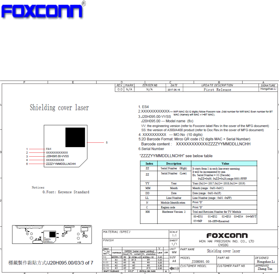
13 Label Information
13.1 MAC ID Label (for ES4,Pre- MP)
Laser marking : China factory
49
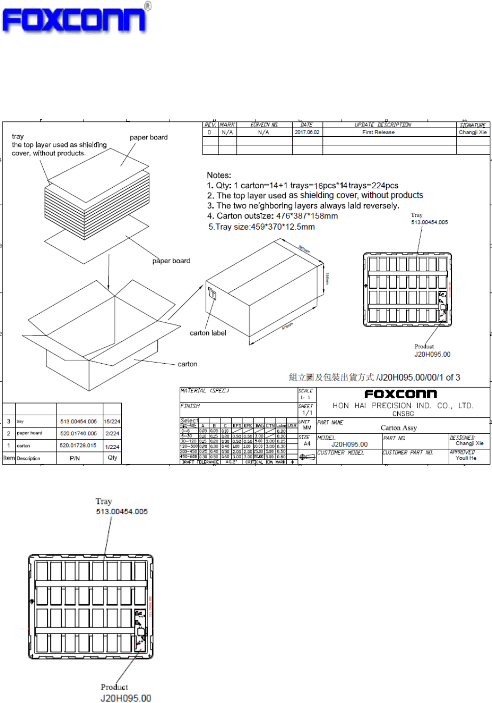
14 Package and Stack Information
14.1 Carton ASSY
14.2 Tray
50
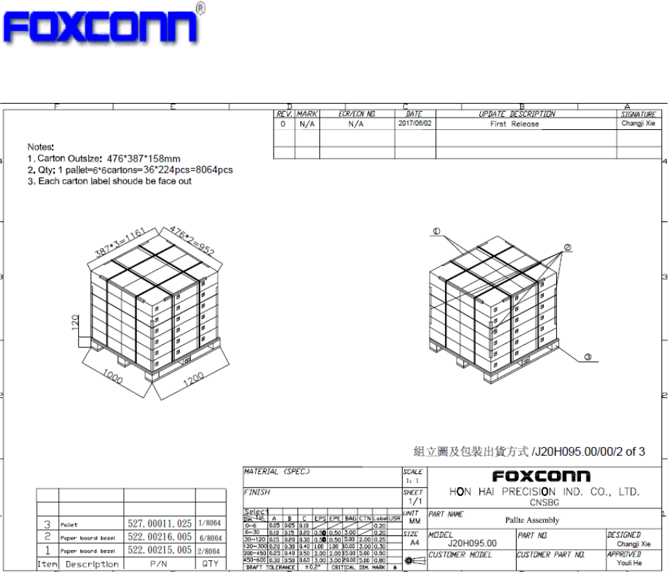
14.3 Pallet ASSY
51
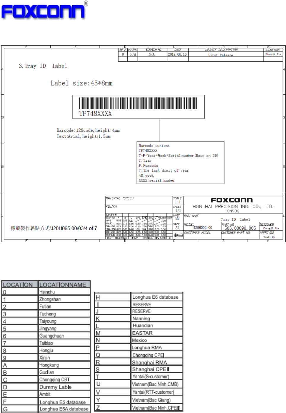
14.4 Tray ID Label
14.5 Carton Label
Instruction For Location Code
52
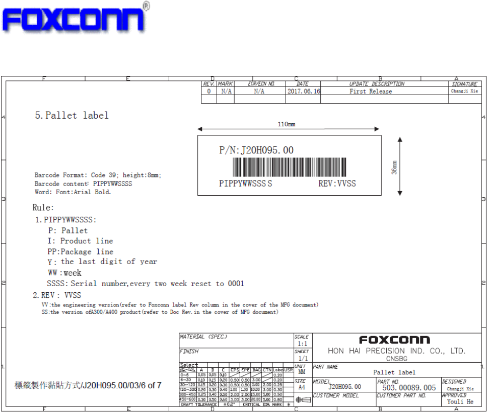
14.6 Pallet Label
53
15 Handling Notice
1) ESD
There are semiconductors on the module, please handle the module under ESD protected
and well-controlled environment (<1500V).

54
16 Reliability Test Result
No. Testing Chamber Location Qty
Test
Duration Status
1 High Temperature Load Test HT15 NN-SQA A:2pcs
B:2pcs 2 days Pass
2 Low Temperature Load Test TBD NN-SQA A:2pcs
B:2pcs 2 days Pass
3 Low Temperature Storage Test HT06 NN-SQA A:2pcs
B:2pcs 45 days TBD
4 High Temperatureand Humidity
Storage Test HT06 NN-SQA
A:2pcs
B:2pcs 45 days TBD
5 High Temperature and Humidity
Cycle Test HT06 NN-SQA
A:4pcs
B:4pcs 6 days TBD
6 High Temperature and Operation
Test HT11 NN-SQA
A:2pcs
B:2pcs 45 days TBD
7 High Temperature and Humidity
Operation Test HT11 NN-SQA
A:2pcs
B:2pcs 45 days TBD
8 Thermal Shock Test & Cross
section inspection
Themal shock
chamber NN-SQA A:5pcs
B:5pcs
29 days Pass
Cross-section 7 days Pass
9 Vibration Test Vibration tester NN-SQA A:2pcs
B:2pcs
2 days TBD
Cross-section 7 days TBD
10 Impact Test Shock tester LH A:2pcs
B:2pcs
14 days TBD
Cross-section 7 days TBD
11 Atmospheric Preconditioning TBD NN-SQA 1 Carton 4 days TBD
12 Compression Test(with package) / NN-SQA 1 Carton 3 days TBD
13 Random Vibration Test (with
package) / NN-SQA 1 Carton 3 days TBD
14 Drop Test (with package) / NN-SQA 1 Carton 1 day TBD
15 Sinus Vibration Test (with package) / NN-SQA 1 Carton 1 day TBD
FederalCommunicationCommissionInterferenceStatement
ThisdevicecomplieswithPart15oftheFCCRules.Operationissubjecttothe
followingtwoconditions:(1)Thisdevicemaynotcauseharmfulinterference,and(2)
thisdevicemustacceptanyinterferencereceived,includinginterferencethatmay
causeundesiredoperation.
ThisequipmenthasbeentestedandfoundtocomplywiththelimitsforaClassB
digitaldevice,pursuanttoPart15oftheFCCRules.Theselimitsaredesignedto
providereasonableprotectionagainstharmfulinterferenceinaresidential
installation.Thisequipmentgenerates,usesandcanradiateradiofrequencyenergy
and,ifnotinstalledandusedinaccordancewiththeinstructions,maycauseharmful
interferencetoradiocommunications.However,thereisnoguaranteethat
interferencewillnotoccurinaparticularinstallation.Ifthisequipmentdoescause
harmfulinterferencetoradioortelevisionreception,whichcanbedeterminedby
turningtheequipmentoffandon,theuserisencouragedtotrytocorrectthe
interferencebyoneofthefollowingmeasures:
‐ Reorientorrelocatethereceivingantenna.
‐ Increasetheseparationbetweentheequipmentandreceiver.
‐ Connecttheequipmentintoanoutletonacircuitdifferentfromthat
towhichthereceiverisconnected.
‐ Consultthedealeroranexperiencedradio/TVtechnicianforhelp.
FCCCaution:Anychangesormodificationsnotexpresslyapprovedbytheparty
responsibleforcompliancecouldvoidtheuser'sauthoritytooperatethisequipment.
Thistransmittermustnotbeco‐locatedoroperatinginconjunctionwithanyother
antennaortransmitter.
RadiationExposureStatement:
ThisequipmentcomplieswithFCCradiationexposurelimitssetforthforan
uncontrolledenvironment.Thisequipmentshouldbeinstalledandoperatedwith
minimumdistance20cmbetweentheradiator&yourbody.

ThisdeviceisintendedonlyforOEMintegratorsunderthefollowingconditions:
Theantennamustbeinstalledsuchthat20cmismaintainedbetweentheantenna
andusers,and
Thetransmittermodulemaynotbeco‐locatedwithanyothertransmitterorantenna.
Aslongas2conditionsabovearemet,furthertransmittertestwillnotberequired.
However,theOEMintegratorisstillresponsiblefortestingtheirend‐productforany
additionalcompliancerequirementsrequiredwiththismoduleinstalled
IMPORTANTNOTE:Intheeventthattheseconditionscannotbemet(forexample
certainlaptopconfigurationsorco‐locationwithanothertransmitter),thentheFCC
authorizationisnolongerconsideredvalidandtheFCCIDcannotbeusedonthe
finalproduct.Inthesecircumstances,theOEMintegratorwillberesponsibleforre‐
evaluatingtheendproduct(includingthetransmitter)andobtainingaseparateFCC
authorization.
EndProductLabeling
Thistransmittermoduleisauthorizedonlyforuseindevicewheretheantennamay
beinstalledsuchthat20cmmaybemaintainedbetweentheantennaandusers.The
finalendproductmustbelabeledinavisibleareawiththefollowing:“ContainsFCC
ID:AK8J20H095”.Thegrantee'sFCCIDcanbeusedonlywhenallFCCcompliance
requirementsaremet.
ManualInformationTotheEndUser
TheOEMintegratorhastobeawarenottoprovideinformationtotheenduser
regardinghowtoinstallorremovethisRFmoduleintheuser’smanualoftheend
productwhichintegratesthismodule.
Theendusermanualshallincludeallrequiredregulatoryinformation/warningas
showinthismanual.
IndustryCanadastatement:
ThisdevicecomplieswithISED’slicence‐exemptRSSs.Operationissubjecttothe
followingtwoconditions:(1)Thisdevicemaynotcauseharmfulinterference,and(2)
thisdevicemustacceptanyinterferencereceived,includinginterferencethatmay
causeundesiredoperation.
LeprésentappareilestconformeauxCNRd’ISEDapplicablesauxappareilsradio
exemptsdelicence.L’exploitationestautoriséeauxdeuxconditionssuivantes:(1)le
dispositifnedoitpasproduiredebrouillagepréjudiciable,et(2)cedispositifdoit
acceptertoutbrouillagereçu,ycomprisunbrouillagesusceptibledeprovoquerun
fonctionnementindésirable.
RadiationExposureStatement:
ThisequipmentcomplieswithISEDradiationexposurelimitssetforthforan
uncontrolledenvironment.Thisequipmentshouldbeinstalledandoperatedwith
minimumdistance20cmbetweentheradiator&yourbody.
Déclarationd'expositionauxradiations:
Cetéquipementestconformeauxlimitesd'expositionauxrayonnementsISED
établiespourunenvironnementnoncontrôlé.Cetéquipementdoitêtreinstalléet
utiliséavecunminimumde20cmdedistanceentrelasourcederayonnementet
votrecorps.
ThisdeviceisintendedonlyforOEMintegratorsunderthefollowingconditions:(For
moduledeviceuse)
1)Theantennamustbeinstalledsuchthat20cmismaintainedbetweentheantenna
andusers,and
2)Thetransmittermodulemaynotbeco‐locatedwithanyothertransmitteror
antenna.
Aslongas2conditionsabovearemet,furthertransmittertestwillnotberequired.
However,theOEMintegratorisstillresponsiblefortestingtheirend‐productforany
additionalcompliancerequirementsrequiredwiththismoduleinstalled.
CetappareilestconçuuniquementpourlesintégrateursOEMdanslesconditions
suivantes:(Pourutilisationdedispositifmodule)
1)L'antennedoitêtreinstalléedetellesortequ'unedistancede20cmestrespectée
entrel'antenneetlesutilisateurs,et
2)Lemoduleémetteurpeutnepasêtrecoïmplantéavecunautreémetteurou
antenne.
Tantqueles2conditionsci‐dessussontremplies,desessaissupplémentairessur
l'émetteurneserontpasnécessaires.Toutefois,l'intégrateurOEMesttoujours
responsabledesessaissursonproduitfinalpourtoutesexigencesdeconformité
supplémentairesrequispourcemoduleinstallé.
IMPORTANTNOTE:
Intheeventthattheseconditionscannotbemet(forexamplecertainlaptop
configurationsorco‐locationwithanothertransmitter),thentheCanada
authorizationisnolongerconsideredvalidandtheICIDcannotbeusedonthefinal
product.Inthesecircumstances,theOEMintegratorwillberesponsibleforre‐
evaluatingtheendproduct(includingthetransmitter)andobtainingaseparate
Canadaauthorization.
NOTEIMPORTANTE:
Danslecasoùcesconditionsnepeuventêtresatisfaites(parexemplepourcertaines
configurationsd'ordinateurportableoudecertainesco‐localisationavecunautre
émetteur),l'autorisationduCanadan'estplusconsidérécommevalideetl'IDICne
peutpasêtreutilisésurleproduitfinal.Danscescirconstances,l'intégrateurOEM
serachargéderéévaluerleproduitfinal(ycomprisl'émetteur)etl'obtentiond'une
autorisationdistincteauCanada.
EndProductLabeling
Thistransmittermoduleisauthorizedonlyforuseindevicewheretheantennamay
beinstalledsuchthat20cmmaybemaintainedbetweentheantennaandusers.The
finalendproductmustbelabeledinavisibleareawiththefollowing:“ContainsIC:
409B‐J20H095”.
Plaquesignalétiqueduproduitfinal
Cemoduleémetteurestautoriséuniquementpouruneutilisationdansundispositif
oùl'antennepeutêtreinstalléedetellesortequ'unedistancede20cmpeutêtre
maintenueentrel'antenneetlesutilisateurs.Leproduitfinaldoitêtreétiquetédans
unendroitvisibleavecl'inscriptionsuivante:"ContientdesIC:409B‐J20H095".
ManualInformationTotheEndUser
TheOEMintegratorhastobeawarenottoprovideinformationtotheenduser
regardinghowtoinstallorremovethisRFmoduleintheuser’smanualoftheend
productwhichintegratesthismodule.
Theendusermanualshallincludeallrequiredregulatoryinformation/warningas
showinthismanual.
Manueld'informationàl'utilisateurfinal
L'intégrateurOEMdoitêtreconscientdenepasfournirdesinformationsà
l'utilisateurfinalquantàlafaçond'installeroudesupprimercemoduleRFdansle
manueldel'utilisateurduproduitfinalquiintègrecemodule.
Lemanueldel'utilisateurfinaldoitincluretouteslesinformationsréglementaires
requisesetavertissementscommeindiquédanscemanuel.
Caution:
(i)thedeviceforoperationintheband5150‐5250MHzisonlyforindooruseto
reducethepotentialforharmfulinterferencetoco‐channelmobilesatellitesystems;
(ii)themaximumantennagainpermittedfordevicesinthebands5250‐5350MHz
and5470‐5725MHzshallbesuchthattheequipmentstillcomplieswiththee.i.r.p.
limit;
(iii)themaximumantennagainpermittedfordevicesintheband5725‐5850MHz
shallbesuchthattheequipmentstillcomplieswiththee.i.r.p.limitsspecifiedfor
point‐to‐pointandnon‐point‐to‐pointoperationasappropriate;and
(iv)theworst‐casetiltangle(s)necessarytoremaincompliantwiththee.i.r.p.
elevationmaskrequirementsetforthinSection6.2.2(3)shallbeclearlyindicated.
(v)Usersshouldalsobeadvisedthathigh‐powerradarsareallocatedasprimary
users(i.e.priorityusers)ofthebands5250‐5350MHzand5650‐5850MHzandthat
theseradarscouldcauseinterferenceand/ordamagetoLE‐LANdevices.
Avertissement:
Leguided’utilisationdesdispositifspourréseauxlocauxdoitincluredesinstructions
précisessurlesrestrictionssusmentionnées,notamment:
(i)lesdispositifsfonctionnantdanslabande5150‐5250MHzsontréservés
uniquementpouruneutilisationàl’intérieurafinderéduirelesrisquesdebrouillage
préjudiciableauxsystèmesdesatellitesmobilesutilisantlesmêmescanaux;
(ii)legainmaximald'antennepermispourlesdispositifsutilisantlesbandesde5250
à5350MHzetde5470à5725MHzdoitêtreconformeàlalimitedelap.i.r.e;
(iii)legainmaximald'antennepermis(pourlesdispositifsutilisantlabandede5725
à5850MHz)doitêtreconformeàlalimitedelap.i.r.e.spécifiéepourl'exploitation
pointàpointetl’exploitationnonpointàpoint,selonlecas;
(iv)lespiresanglesd’inclinaisonnécessairespourresterconformeàl’exigencedela
p.i.r.e.applicableaumasqued’élévation,eténoncéeàlasection6.2.23),doivent
êtreclairementindiqués.
(v)Deplus,lesutilisateursdevraientaussiêtreavisésquelesutilisateursderadarsde
hautepuissancesontdésignésutilisateursprincipaux(c.‐à‐d.,qu’ilsontlapriorité)
pourlesbandes5250‐5350MHzet5650‐5850MHzetquecesradarspourraient
causerdubrouillageet/oudesdommagesauxdispositifsLAN‐EL.

低功率電波輻射性電機管理辦法
第十二條 經型式認證合格之低功率射頻電機,非經許可,公司、商號或使用者均不得
擅自變更頻率、加大功率或變更原設計之特性及功能。
第十四條 低功率射頻電機之使用不得影響飛航安全及干擾合法通信;經發現有干擾現
象時,應立即停用,並改善至無干擾時方得繼續使用。
前項合法通信,指依電信法規定作業之無線電通信。
低功率射頻電機須忍受合法通信或工業、科學及醫療用電波輻射性電機設備
之干擾。
模組認證:
1. 本模組於取得認證後將依規定於模組本體標示審驗合格標籤。
2. 系統廠商應於平台上標示「本產品內含射頻模組: XXXyyyLPDzzzz-x」字樣。