Sony BE001012 CDMA 800 & 1900 MHz/AMPS User Manual Part 90
Sony Mobile Communications Inc CDMA 800 & 1900 MHz/AMPS Part 90
UserManual.wiki
>
Sony
>
BE001012 User Manual
Manual
Navigation menu
Upload a User Manual
Namespaces
Wiki Guide
HTML
PDF
Info
Views
User Manual
Discussion / Help
Navigation
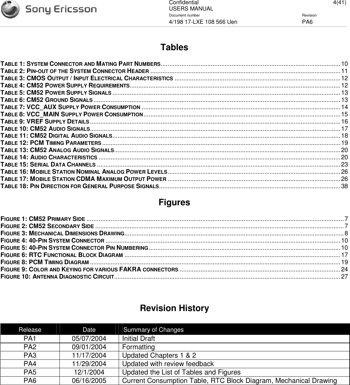
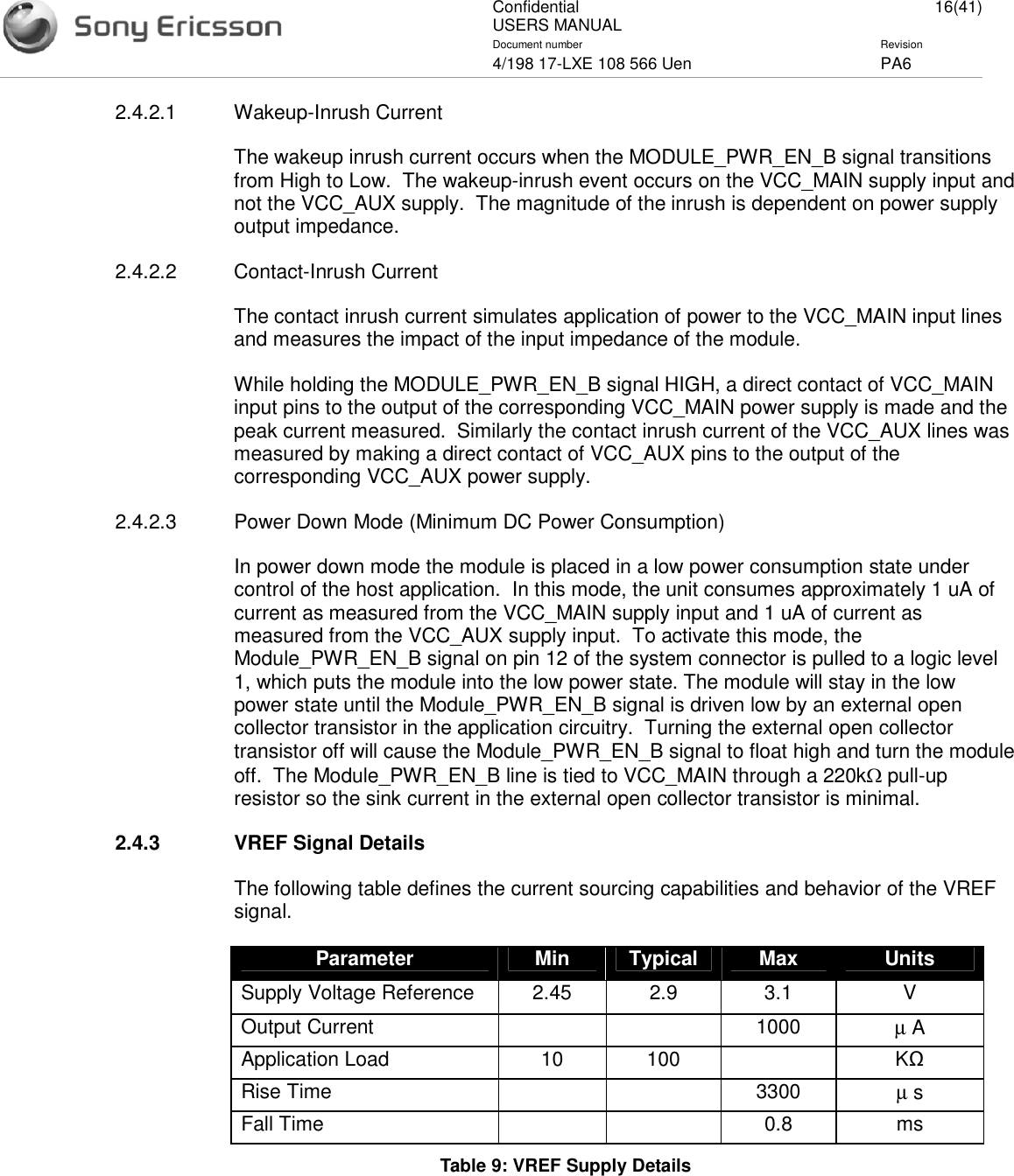
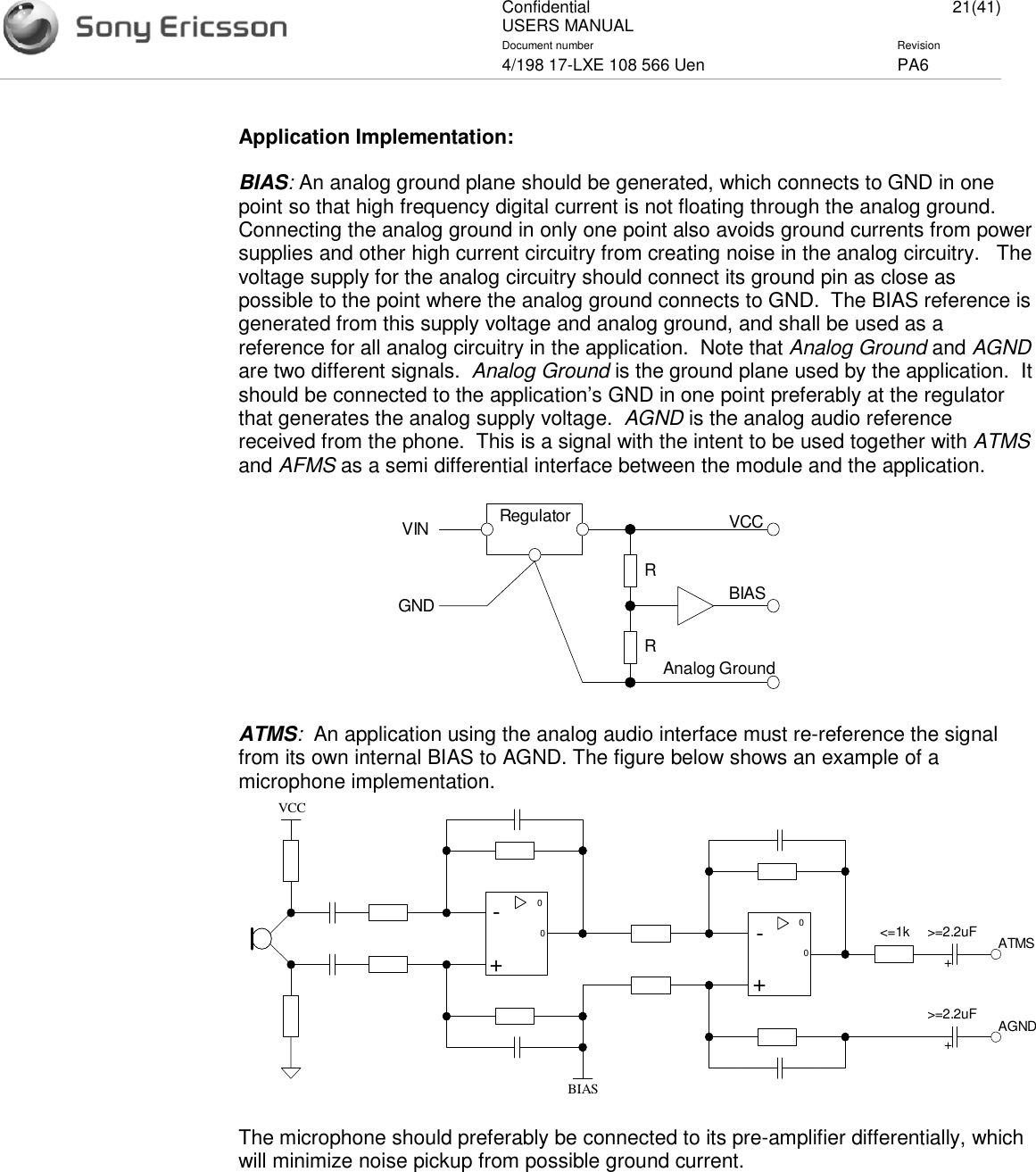
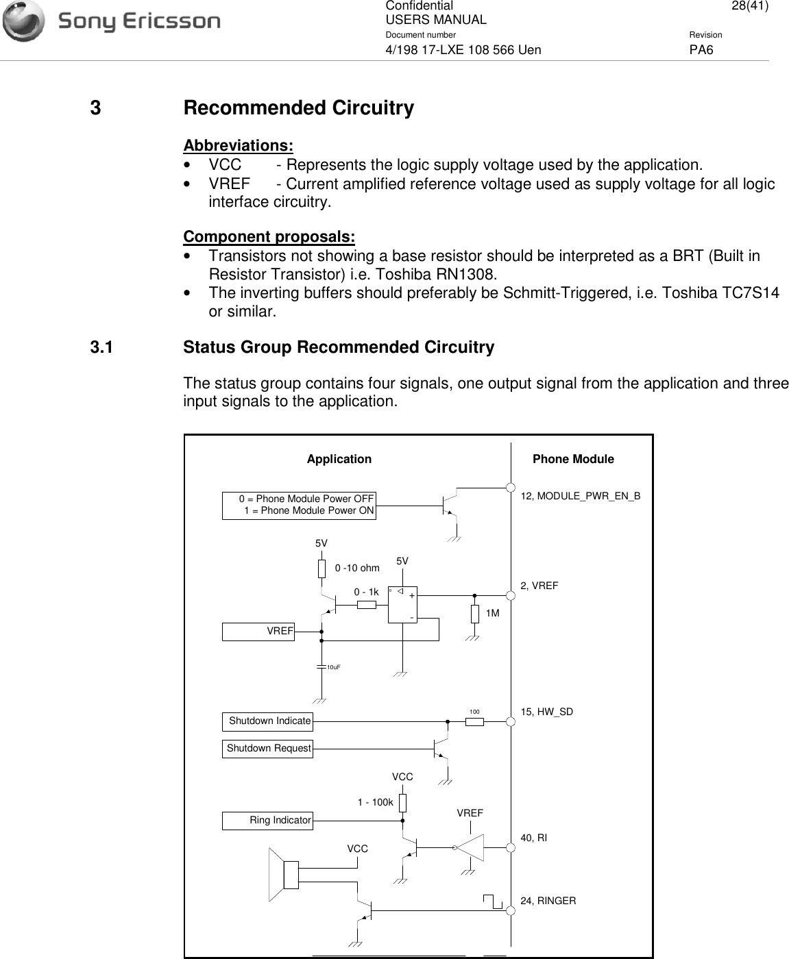
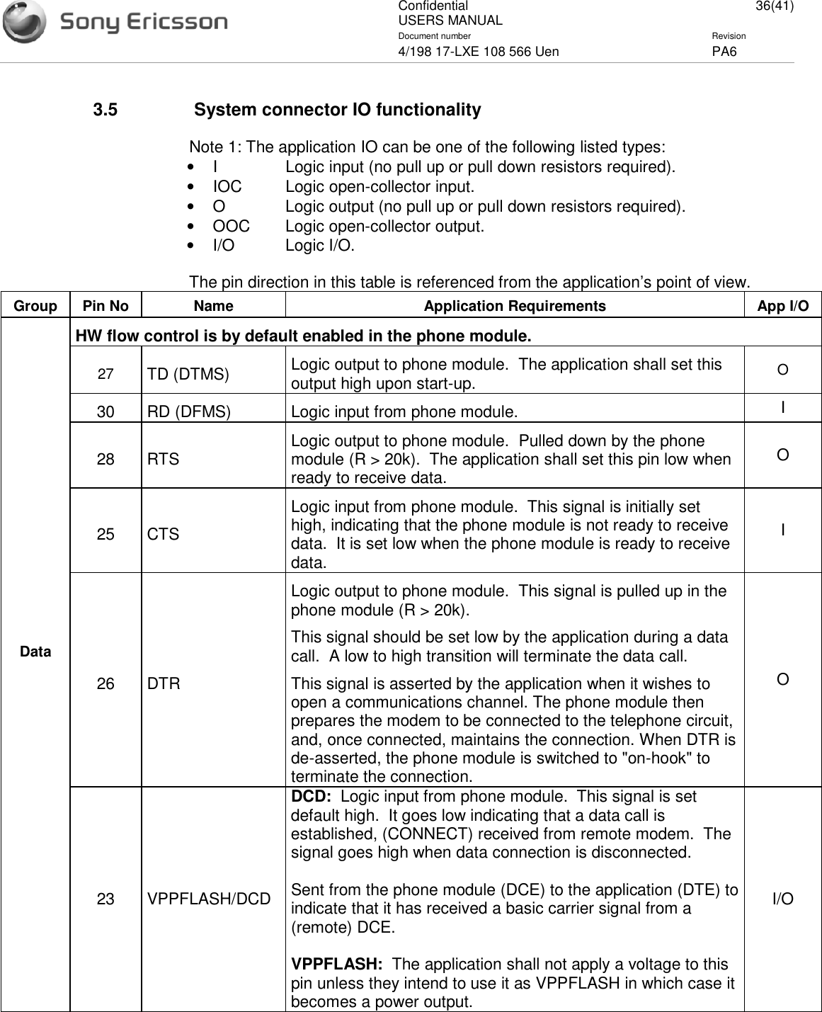
![ConfidentialUSERS MANUAL 14(41)Document number Revision4/198 17-LXE 108 566 Uen PA6[VCC_AUX power supply supports the 3W mode AMPS circuitry]Parameter MinimumValue TypicalValue MaximumValue UnitsInput Voltage 11 13.8 16.6 VIn a Call on Power Level 0(Power Class I) 0.88 1.3 AIn a Call on Power Level 2 3.5 4.5 mAAMPS Burst Duration for networkupdate 0.16 sStand-by/Idle mode (RX ON) 0.5 µAPowered Down Current Draw 1 µAInrush Current (Entering PL0) 16 ADuration of Inrush (Entering PL0) 40 µsInrush Current (contact) 28 ADuration of Inrush (contact) 40 µsTable 7: VCC_AUX Supply Power ConsumptionNote: The typical values observed in AMPS call are made with voice channel set at358.](https://usermanual.wiki/Sony/BE001012/User-Guide-570718-Page-15.png)
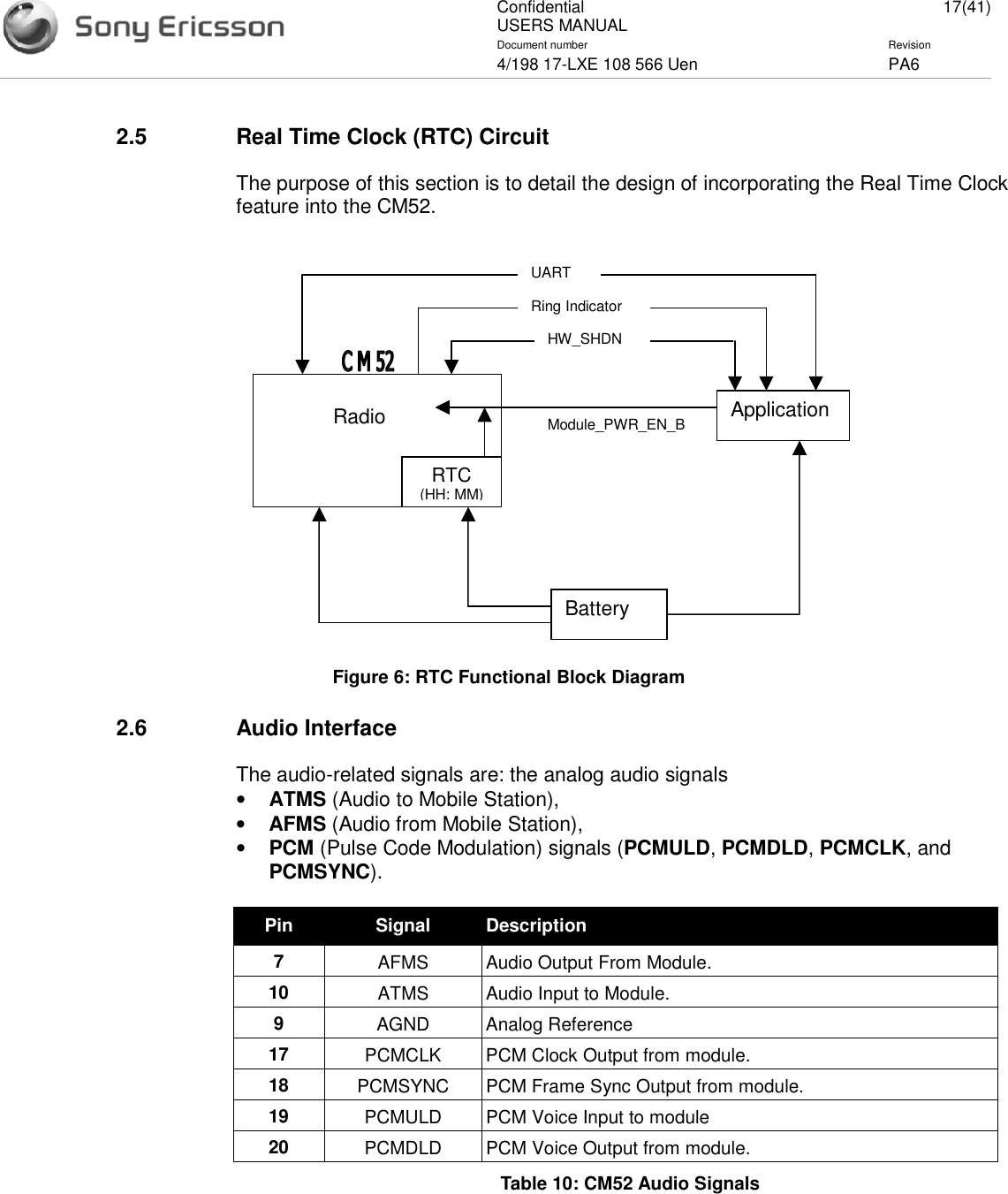
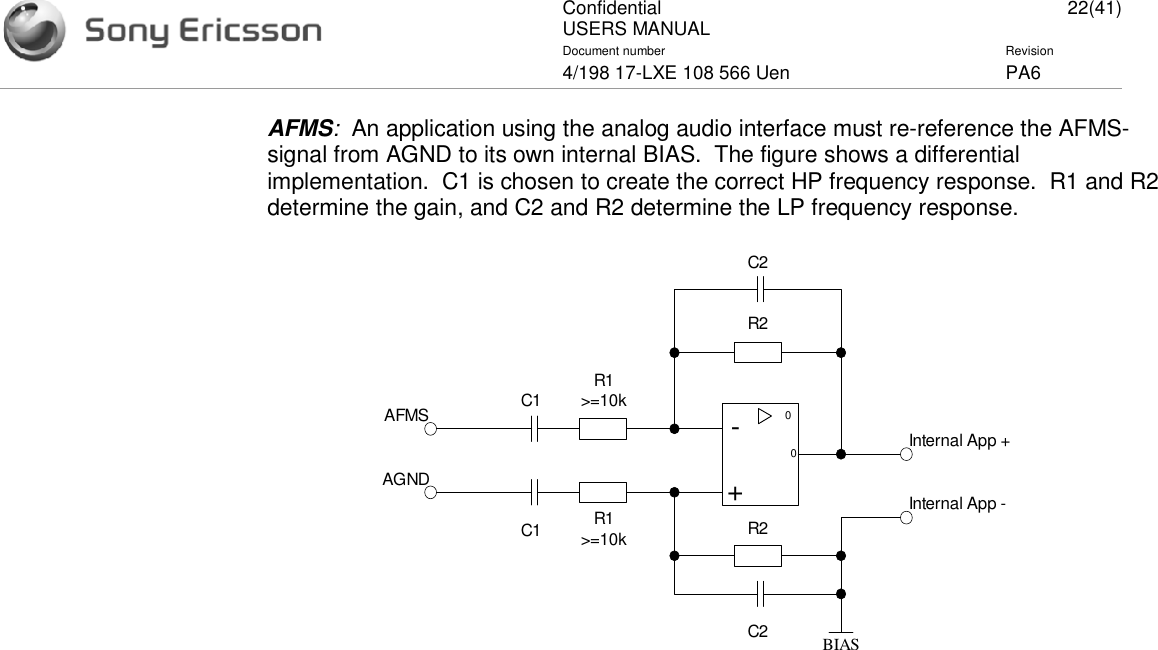
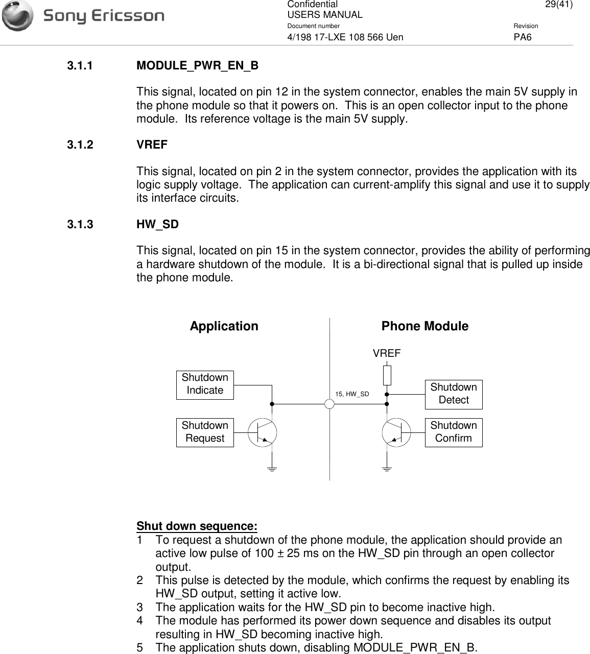
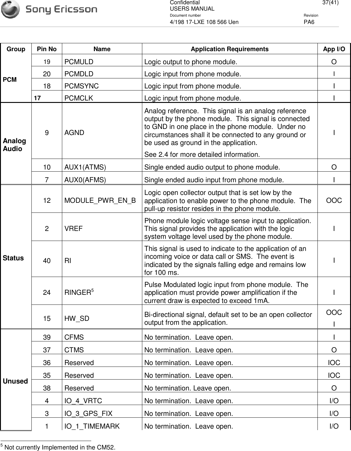
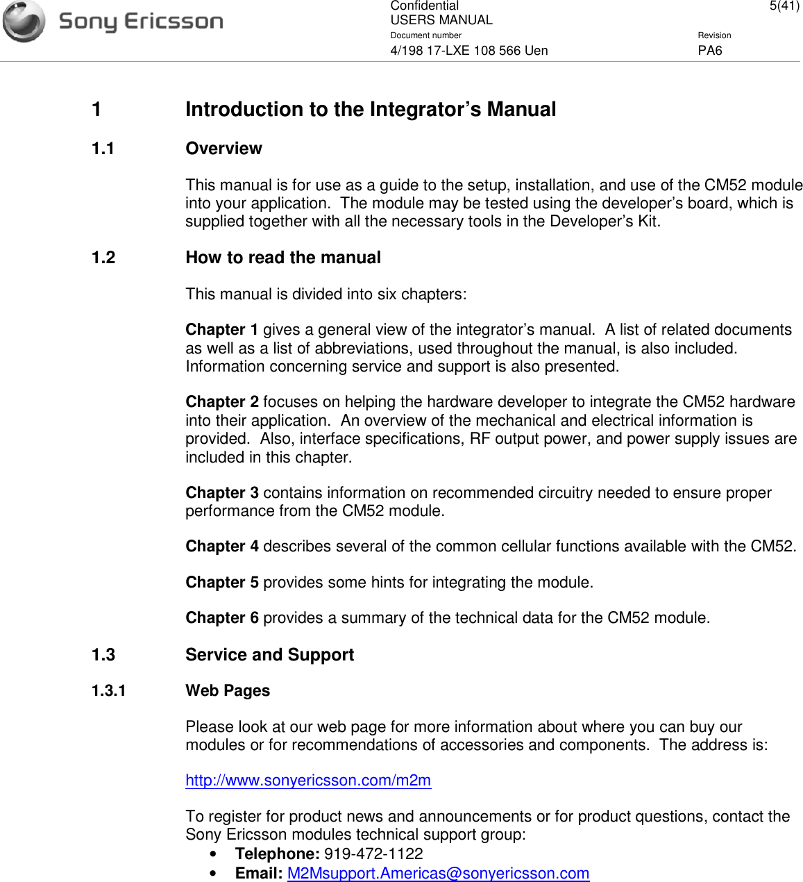
![ConfidentialUSERS MANUAL 15(41)Document number Revision4/198 17-LXE 108 566 Uen PA6[VCC_MAIN supply is the primary CM52 power supply]Parameter MinimumValue TypicalValue MaximumValue UnitsInput Voltage 4.5 5 5.5 VIn AMPS Call on Power Level 0(Power Class I) 0.59 0.75 AIn AMPS Call on Power Level 2 0.83 1.0 AIn CDMA call-Cellular Mode 0.67 0.90 AIn CDMA call-PCS Mode 0.72 0.95 A CDMA burst duration for Networkupdate 1.2 SStandby/Idle Current Draw inSlotted Mode (CDMA)1.28 sec slot 9.6 mA2.56 sec slot 7.2 mA5.12 sec slot 4.5 mAStand-by/Idle mode (AMPS) 45 mAPowered Down Current Draw 1 µAInrush Current (on wake up) 2.2 ADuration of Inrush (on wake-up) 150 µsInrush Current (contact) 2.0 ADuration of Inrush (contact) 50 µsTable 8: VCC_MAIN Supply Power ConsumptionNotes1. The typical current measurements noted in CDMA mode are with the followingsettings:a. CDMA-Cellular (800MHz): Band = IS-2000, Cell-Power = -104dBm,Channel Number 358b. CDMA-PCS (1900MHz): Band = IS-2000, Cell-Power = -104dBm,Channel Number 563Maximum Slot Cycle Index for both 800MHz and 1900MHz modes = 12. The inrush current measurements noted here are with respect to the stand aloneCM52 module at room temperature, the results might vary when the CM52 is usedin the Customer Application.3. Measurements are based on worst case scenario—CM52 with 3W option. Valuesfor CM52 with no 3W option could be marginally lower.](https://usermanual.wiki/Sony/BE001012/User-Guide-570718-Page-16.png)