Sony DVP S500D User Manual CD/DVD SYSTEM Manuals And Guides 98060757
SONY DVD Systems Manual 98060757 SONY DVD Systems Owner's Manual, SONY DVD Systems installation guides
DVP-S505D 98060757
User Manual: Sony DVP-S500D DVP-S500D SONY CD/DVD SYSTEM - Manuals and Guides View the owners manual for your SONY CD/DVD SYSTEM #DVPS500D. Home:Electronics Parts:Sony Parts:Sony CD/DVD SYSTEM Manual
Open the PDF directly: View PDF ![]() .
.
Page Count: 78
DVP-M35/S300/S305/S315/
S500D/S 505D/$715
OPERATION MANUAL
_CD/DVD PLAYER
Contents
1. Outline ....................................................................................................................................6
1-1. Series line-up ...............................................................................................................6
1-2. External appearance diagram ..................................................................................7
1-3,.Internal appearance diagram (top view) ..............................................................8
1-4. Disc drive unit ...........................................................................................................10
1-5. Block diagram ........................................................................................................... 13
2. SIGNAL PROCESSING BLOCK ...................................................................15
2-1. DVD RF FRONT END ..........................................................................................15
2-1-1. Attenuation of OP Output Signals ......................................................................... 16
2-1-2. HPF ........................................................................................................................ 16
2-1-3. RF Front End Processing: IC001 SSI33P3720 ...................................................... 16
2-2. CD RF FRONT END ..............................................................................................19
2-3. RF SIGNAL PROCESSING BLOCK ...............................................................2O
2-4. Decrypt Block ...........................................................................................................21
2-5. AV Decoder Block ...................................................................................................21
2-6. OSD Block .................................................................................................................21
L
2-7,. DNR, Video Encoder Blocks ................................................................................23
2-8. Clock Generation Block ......................................................................................... 24
2-9. AC-3 Decoder Block ...............................................................................................25
2-10. Audio L, R 2ch Signal Block .............................................................................26
2-11. Audio 5. lch Signal Block ....................................................................................27
2-12. DVP-S715 AU-205 Board Block Diagram ....................................................28
2-13. System Control Block ...........................................................................................29
2-14. Interface Control Block ........................................................................................29
3. SERVO BLOCK ...........................................................................................................33
3-1. General Description of Servo Circuits ............................................................... 33
3-1-1. Optical Pickup Control .......................................................................................... 33
3-1-2. Sled Control ........................................................................................................... 33
3-1-3. Spindle Control ...................................................................................................... 33
3-1-4. Tilt Control ............................................................................................................ 33
3-I-5. Disc Loading and Chucking .................................................................................. 33
3-1-6. Disc Judgment ....................................................................................................... 33
3-2. Servo Operation at DVD Play .............................................................................. 34
3-2-1. Optical Pickup Control .......................................................................................... 34
3-2-2. Sled Control ........................................................................................................... 41
3-2-3. Spindle Control ...................................................................................................... 43
3-2-4. Tilt Control ............................................................................................................ 44
3-3. Servo Operation at CD and Video CD Playing ...............................................46
3-3-1. Optical Pickup Control .......................................................................................... 46
3-3-2. Sled Control ........................................................................................................... 50
3-3-3. Spindle Control ...................................................................................................... 50
3-3-4. Tilt Control ......................................................................... :.................................. 50
3-4. Disc Loading and Chucking ..................................................................................50
3-4-1. Motor Driver .......................................................................................................... 51
3-4-2. Tray Position Detection ......................................................................................... 51
3-5. Differentiation of Disk Type ................................................................... 52
3-5-1. CD/DVD Differentiation ........................................................................................ 52
3-5-2. SL/DL Differentiation ............................................................................................ 52
3-5-3. Differentiation ............ i........................................................................................... 52
3-6. Block Diagram (Servo) ...........................................................................................53
4. IC PIN DESCRIPTION ..........................................................................................55
4-1. ARP CXD1865R (IC806 on MB-80 board) .....................................................55
4-1-1. Block Diagram .................................................................................... ................... 55
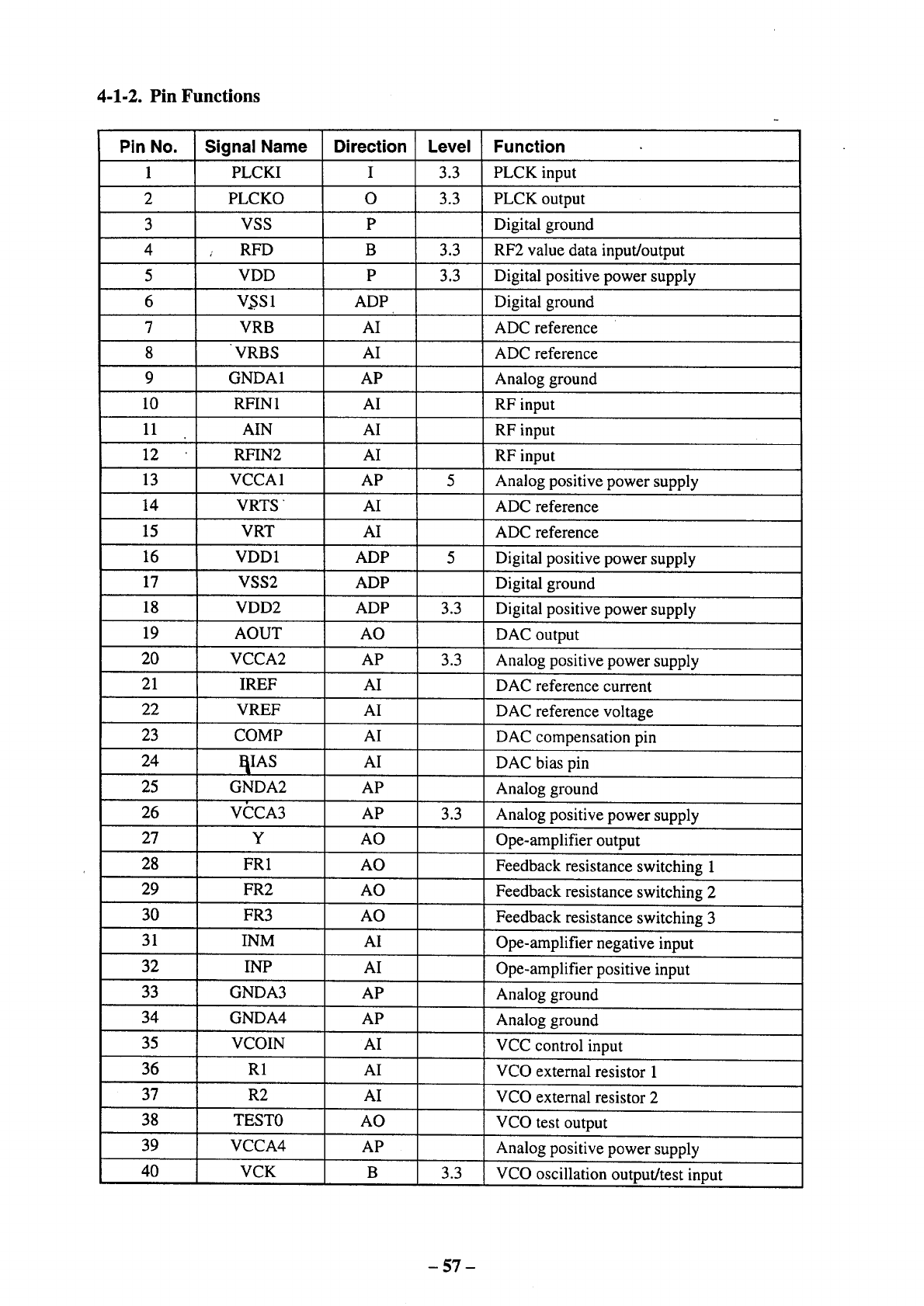
4-1-2. Pin Functions ....................................................................................... '.................. 57
4-2. AV Decoder L64020 (IC203 on MB-78 board) ..............................................62
4-2-1. Block Diagram ....................................................................................................... 62
4-2-2. Pin Assignment ...................................................................................................... 63
4-3. Digital Signal Processor CXD8730R (1C506 on MB;.78 board) ............... 65
4-3:1. Pin Assignment ...................................................................................................... 65
4-3-2. Pin Functions ......................................................................................................... 66
4-4. AC-3 Decoder MB86342 (IC104 on MB-78 board) ......................................70
4-4-1. Block Diagram ....................................................................................................... 70
4-4-2. Pin Functions ......................................................................................................... 71
-4-
4-5. Large Gate Array CXD8728 (IC804 on MB-78 board) ................................ 72
4-5-1. Block Diagram .................................................................................................... 7..72
4-5-2. Pin Functions ........................................................................................................ 73
4-6. Middle Gate Array CXD8746 (IC 101 on MB-78 board) ............................. 78
4-6-1. Block Diagram ....................................................................................................... 78
4-6-2. Pin Functions ......................................................................................................... 79
'4-7. Small Gate Array CXD8747 (IC807 on MB-78 board) ............................... 81
4-7-1. Block Diagram ....................................................................................................... 81
4-7-2. Pin Assignment ..................................... ............................ :.................................... 82
5. OVERALL BLOCK DIAGRAM ......................................................................83
5-1. RF, Servo, Audio, Power Block Diagram ......................................................... 83
5-2. Signal Processing Block Diagram ....................................................................... 89
5
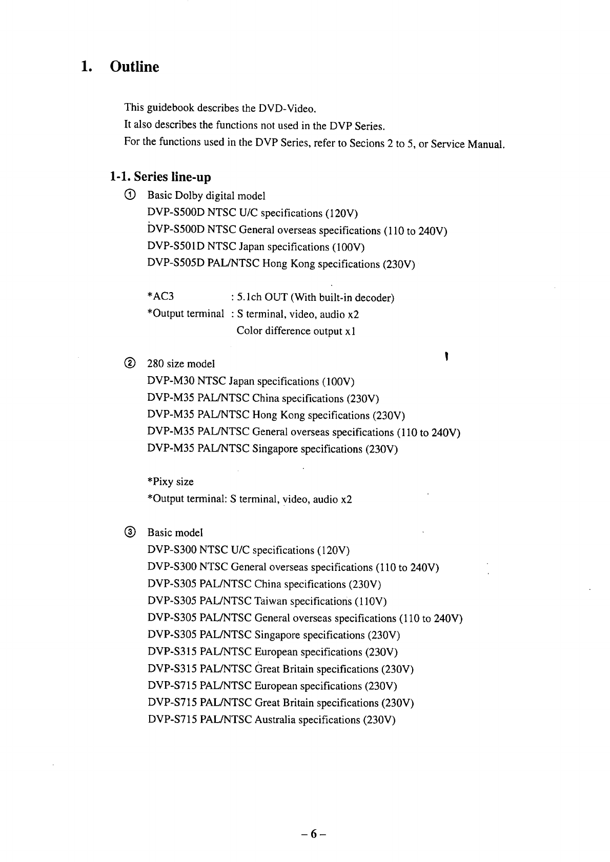
1. Outline
This guidebook describes the DVD-Video.
It also describes the functions not used in the DVP Series.
For the functions used in the DVP Series, refer to Secions 2 to 5, or Service Manual.
1-1. Series line-up
O Basic Dolby digital model
DVP-S500D NTSC U/C specifications (120V)
DVP-S500D NTSC General overseas specifications (110 to 240V)
DVP-S501D NTSC Japan specifications (100V)
DVP-S505D PAL/NTSC Hong Kong specifications (230V)
®
*AC3
*Output terminal
: 5.1 ch OUT (With built-in decoder)
: S terminal, video, audio x2
Color difference output xl
280 size model
DVP-M30 NTSC Japan specifications (100V)
DVP-M35 PAL/NTSC China specifications (230V)
DVP-M35 PAL/NTSC Hong Kong specifications (230V)
DVP-M35 PAL/NTSC General overseas specifications (110 to 240V)
DVP-M35 PAL/NTSC Singapore specifications (230V)
®
*Pixy size
*Output terminal: S terminal, video, audio x2
Basic model
DVP-S300 NTSC U/C specifications (120V)
DVP-S300 NTSC General overseas specifications (110 to 240V)
DVP-S305 PAL/NTSC China specifications (230V)
DVP-S305 PAL/NTSC Taiwan specifications (ll0V)
DVP-S305 PAL/NTSC General overseas specifications (110 to 240V)
DVP,S305 PAL/NTSC
DVP- $315 PAL/NTSC
DVP-S315 PAL/NTSC
DVP-S715 PAL/NTSC
Singapore specifications (230¥)
European specifications (230V)
Great Britain specifications (230V)
European specifications (230V)
DVP-S715 PAL/NTSC Great Britain specifications (230V)
DVP-S715 PAL/NTSC Australia specifications (230V)
-6-
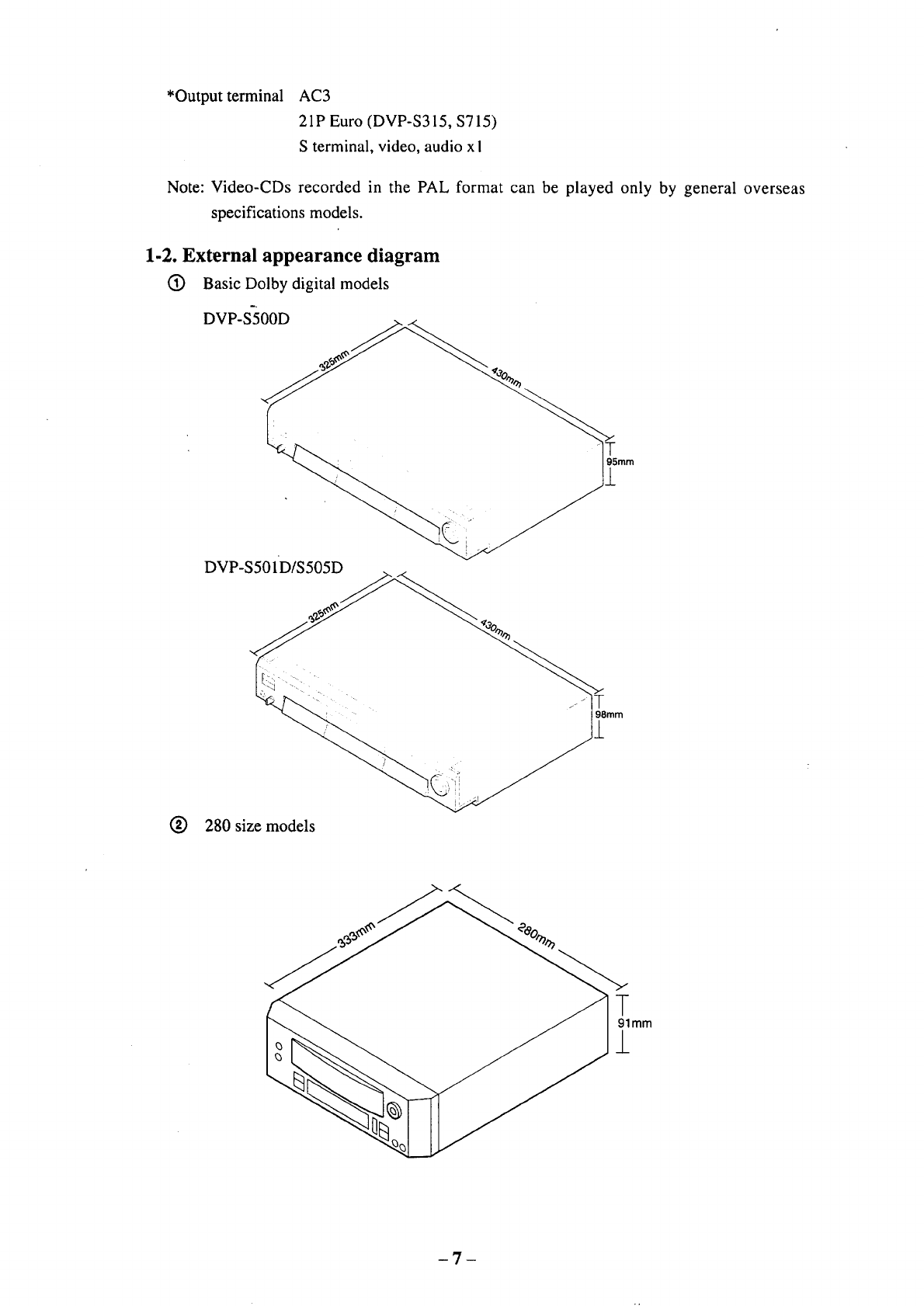
*Output terminal AC3
21P Euro (DVP-S315, $715)
S terminal, video, audio x l
Note: Video-CDs recorded in the PAL format can be played only by general overseas
specifications models.
1-2. External appearance diagram
(_) Basic Dolby digital models
DVP-S'500D
DVP-S501D/S505D
98ram
±
(_) 280 size models
T
91mm
1
7
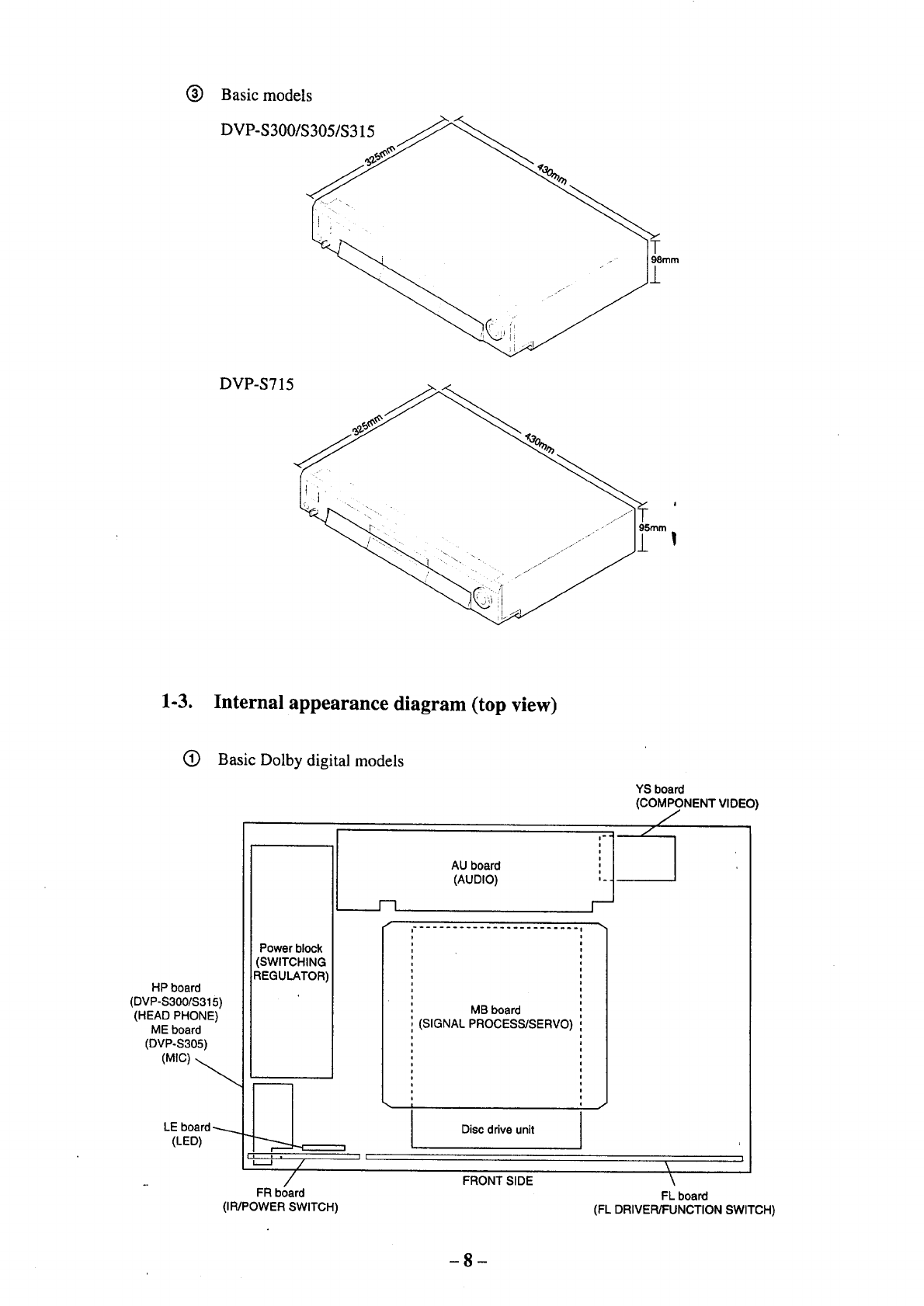
(_ Basic models
DVP-S300/S305/S315
±
DVP-S715
i
!
1-3. Internal appearance diagram (top view)
(_) Basic Dolby digital models
HP board
(DVP-S300/S315)
(HEAD PHONE)
ME board
(DVP-S305)
(MIC)
LE board
(LED)
Power block
(SWITCHING
REGULATOR
';---; '/
/
FR board
(IR/POWER SWITCH)
.__.__F3
AU board
(AUDIO)
.........................
I
MB board
(SIGNAL PROCESS/SERVO)
YS board
(COMPONENT VIDEO)
J
iDisc drive unit
FRONT SIDE
i
1
i
\
FL board
(FL DRIVER/FUNCTION SWITCH)
8
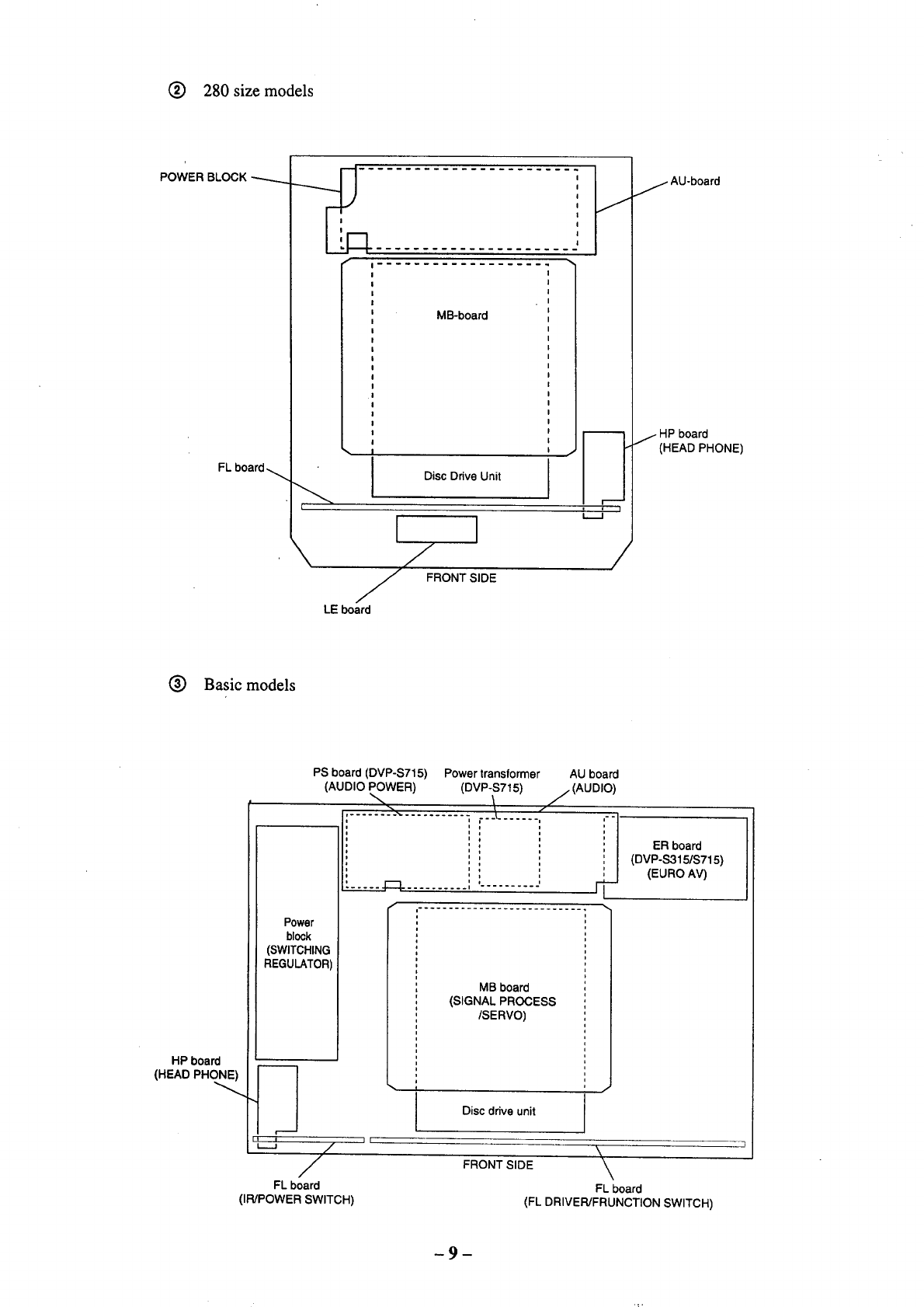
(_) 280 size models
POWER BLOCK _..
FL board
MB-board
--....,
\
Io,sco ,vou , i
I I
/
FRONT SIDE
LE board
, , '1
ii
/
jAU-board
j HP board
(HEAD PHONE)
(_) Basic models
HP board
(HEAD PHO._
PS board (DVP-S715) Power transformer AU board
(AUDIO POWER) (DVP-S715) ,_ (AUDIO)
............. .......... _t III tIIII111 lIlllll_I ........ JI 111 _Iltl""IIll "
Power
block
(SWITCHING
REGULATOR)
ER board
(DVP-S315/S715)
(EURO AV)
iii f--J I
' ' /
/
FL board
MB board
(SIGNAL PROCESS
/SERVO)
(IR/POWER SWITCH)
Disc drive unit
FRONT SIDE
FL board
(FL DRIVEFVFRUNCTION SWITCH)
9
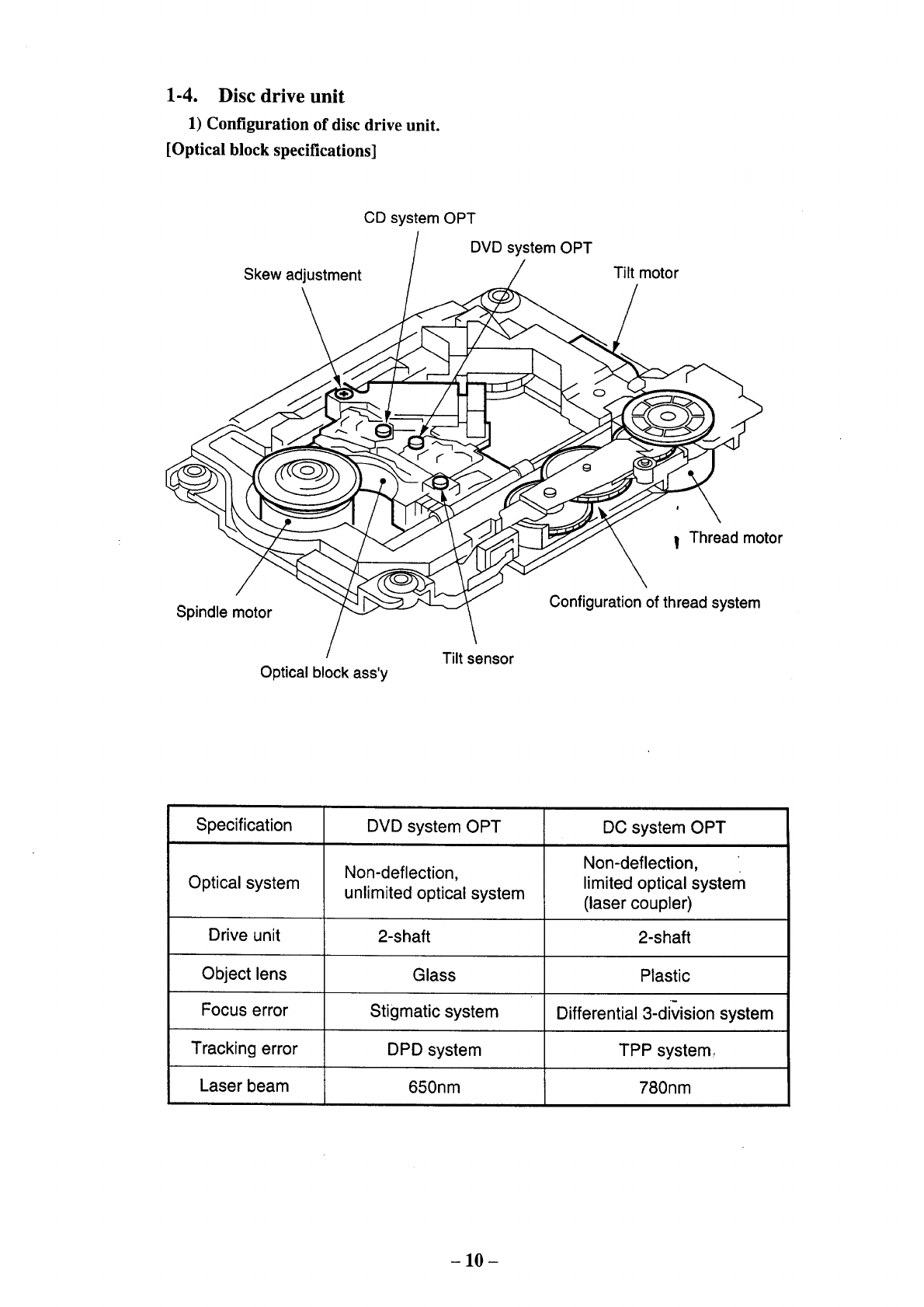
1-4. Disc drive unit
1) Configuration of disc drive unit.
[Optical block specifications]
CD system OPT
Skew adjustment
J
Spindle motor
Optical block ass'y
DVD system OPT
Tilt motor
iThread motor
Configuration of thread system
Tilt sensor
Specification DVD system OPT DC system OPT
Non-deflection,
Non-deflection, limited optical system
Optical system unlimited optical system (laser coupler)
Drive unit 2-shaft 2-shaft
Object lens Glass Plastic
Focus error Stigmatic system Differential 3-division system
Tracking error DPD system TPP system,
Laser beam 650nm 780nm
-10-
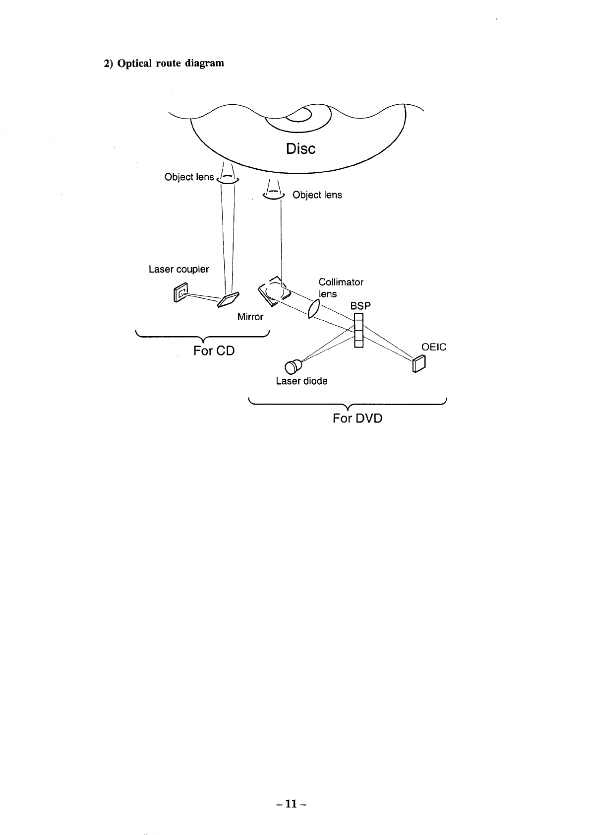
2) Optical route diagram
k
Las Objec ator
_.... lens
Mirror _)_._,._
y J
ForCD (__ ' ' -_"_ OEIC
Laser diode
Y
For DVD
-11-

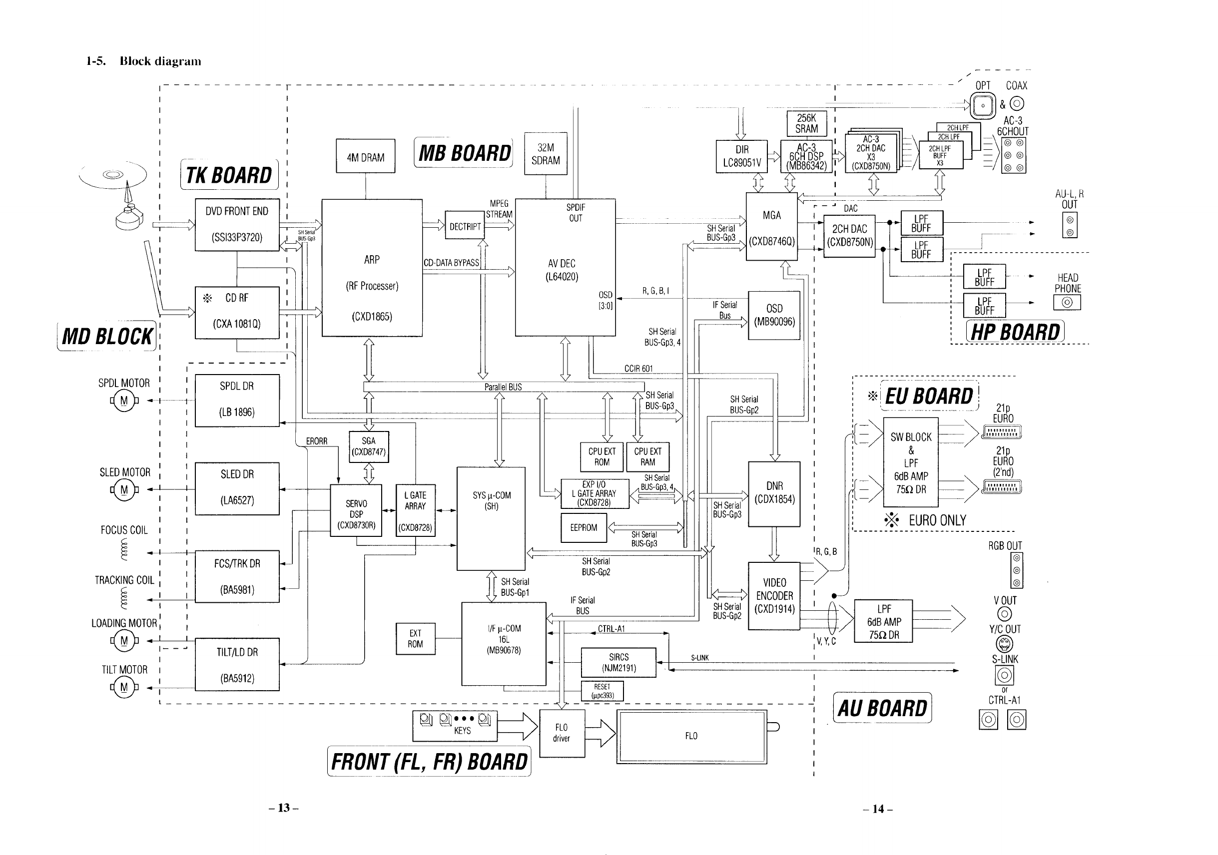
1-5. Block diagram
©
ITKBOARDI
I
_. CDRF
I
SPDLMOTOR I
@ '
SLEDMOTOR
@. ,
I
I
I
FOCUSCOIL I
_ ,i
i
/
/
I............ OPT COAX
TRACKINGCOIL
4M DRAM IMB BOARD132M
SDRAM
.i : &(_)
256K i -_
SRAM I , i 2CHLPF AC-3
ILc8D910R51vH (MBA8C63342)6CHDSP __l]__ _x3 2C_PFB_F___l--;__
...... -_ MGA ____.1 I_ _PF---_ ,..
--- -- SHSerial"l I II 2CHDAC I T-I BUFF I r *
_-- B_(OXD8746Q)[ I_I(oxDa750N)I_I F_
"-_1 _ _ rTCL_ ..........
OSD_ R,G,B,I /ill / ,, --
[3:0] -- IFSerial OSD / , LP.F
SHSerial - Bus_ (MB90096) BUFf /
- s_oo ,4I '11,
CCIR601 ___ II_l[ '- .... .-_------ -------------- -----T ---
__SHSeri_ SHSerial !1 ÷EU BOARD
AI IIBUS-Gp'_BUS-ep2_ ,.................... P21p
4_4_
SPDIF
OUT
LOADINGMOTOR
_I- - ""
I
TILTMOTOR I
®, t
DVDFRONTEND
(SSI33P3720)
'i
I
(CXA1081Q)
[
AVDEC
(L64020)
MPEG
ARP
(RFProcesser)
(CXD1865)
CPRUoEMXTIICPRuAEMxT
.IEXPi-qTd--:_
L GATEARRAY
1_(CXD8728) l_
I E_o_<___ >
_-- SHSera
/1
AU-L,R
OUT
D
HEAD
PHONE
OARDI
I EURO
[ZJ SWBLOCK
& 21p
'v' LPF EURO
IISHSerial (CDX1854) L----J 75aDR
BUS-G"3/_ "_ EUROONLY RGBOUT
IR,G,B
BUS-Gp2 U
VIDEO
IFSerial I1<_ ENCODER I
BUS SHSerial (CXD1914)
BUS-Gp2
S-LINK
FLO
driver
CTRL-A1
FLO
LPF
6dBAMP
75_ DR
V OUT
©
__i) Y/OOUZ
@
S-LINK
-_
or
SPDLDR ParallelBUS
Z
1411
(LB1896)
ERORR SGAI
SLEDDR
(LA6527)
FCS!FRKDR
(BA5981) SHSerialBUS-Gpl
I/Fp-COM
16L
(MB90678)
H lG
SERVO ARI
DSP
(CXD8730R)i I(C×D
I
SIRCS(NJM2191)
RESETI
(ppc393) I
7-
1
TILT/LDDR l" "_
1
(BA5912)
_E
IAY
}728)
SYSp-COM
(SH)
i
F_ONT(FL, FR)BOAR_
CTRL-A1
1,4.
-13- -14 -
2. Signal Processing Block
Block which perfornls various signal proccssings from the RF frollt cnd to the output of
the audio signal and video signal.
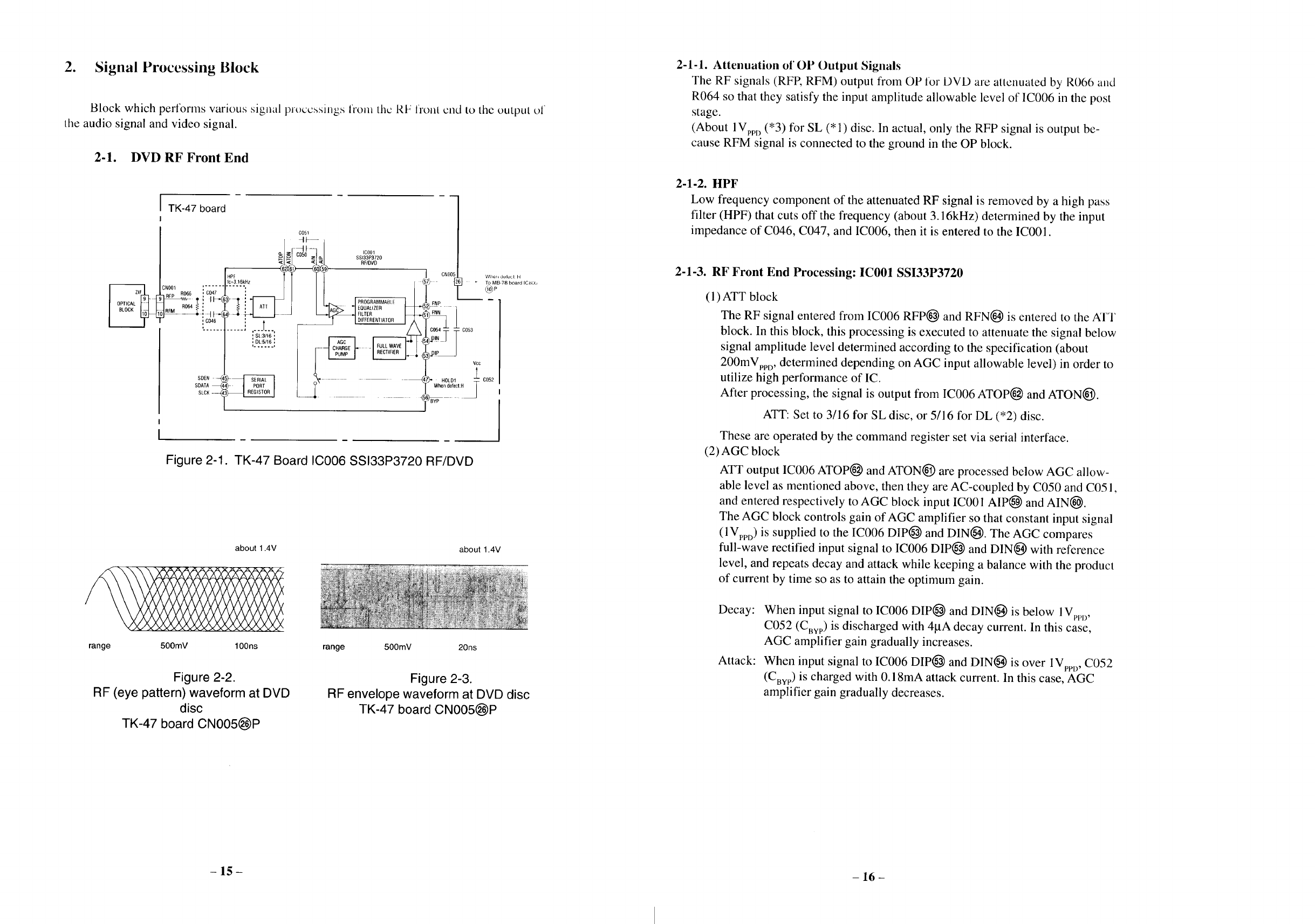
2-1. DVD RF Front End
TK-47 board
0051
oo o ,coo,
8SI33P3720
_ _ _ RFIDVD
IC=3.16kHz
CR001
R066 ,0047
.ru ._ - t F_ 4)
i0046
...L..
' SL:3 6
', DL:5/16 !
SDEN --
SDATA
SLCK
',V_a..,,,,o0_ <"
i 17171ii ,
CNO0_
_When delecl H
TO MB-78 board ICs0b
_ _- c053
_.,.T T
]_D IP_ VCC
Figure 2-1. TK-47 Board IC006 SSI33P3720 RF/DVD
about 1.4V about 1.4V
range 500mV lO0ns range 500mV 20ns
Figure 2-2.
RF (eye pattern) waveform at DVD
disc
TK-47 board CN005_)P
Figure 2-3.
RF envelope waveform at DVD disc
TK-47 board CN005(_P
2-1-1. Attenuation of OP Output Signals
The RF signals (RFP, RFM) output from OP for DVD are attenuated by R066 and
R064 so that they satisfy the input amplitude allowable level of IC006 in the post
stage.
(About IVpp D (*'3) for SL (*1) disc. In actual, only the RFP signal is output be-
cause RFM signal is connected to the ground in the OP block.
2-1-2. ttPF
Low frequency component of the attenuated RF signal is removed by a high pass
filter (HPF) that cuts off the frequency (about 3.16kHz) determined by the input
impedance of C046, C047, and IC006, then it is entered to the IC001.
2-1-3. RF Front End Processing: IC001 SSI33P3720
(1) ATT block
The RF signal entered from IC006 RFP(_) and RFN(_ is entered to the ATT
block. In this block, this processing is executed to attenuate the signal below
signal amplitude level determined according to the specification (about
200mVwD, determined depending on AGC input allowable level) in order to
utilize high performance of IC.
After processing, the signal is output from IC006 ATOP_ and ATONe).
ATT: Set to 3/16 for SL disc, or 5/16 for DL (*2) disc.
These are operated by the command register set via serial interface.
(2) AGC block
ATT output IC006 ATOP(_ and ATONe) are processed below AGC allow-
able level as mentioned above, then they are AC-coupled by C050 and C051,
and entered respectively to AGC block input IC001 AIP_ and AIN(_.
The AGC block controls gain of AGC amplifier so that constant input signal
(1VppD) is supplied to the IC006 DIP@ and DIN_). The AGC compares
full-wave rectified input signal to IC006 DIP(_ and DIN(_) with reference
level, and repeats decay and attack while keeping a balance with the product
of current by time so as to attain the optimum gain.
Decay:
Attack:
When input signal to IC006 DIP(_ and DIN(_) is below I Vppl) ,
C052 (CByp) is discharged with 41aA decay current. In this case,
AGC amplifier gain gradually increases.
When input signal to IC006 DIP_ and DIN(_) is over 1VpeD, C052
(CuvP) is charged with 0.18mA attack current. In this case, AGC
amplifier gain gradually decreases.
-15 - - 16 -
Theinputsignalto IC006DIP_ andDIN_) isa signalprocessedafterEQblock
mentionedlater.
"1:SingleLayerdisc *2:DualLayerdisc *3:Peakto PeakDifferential
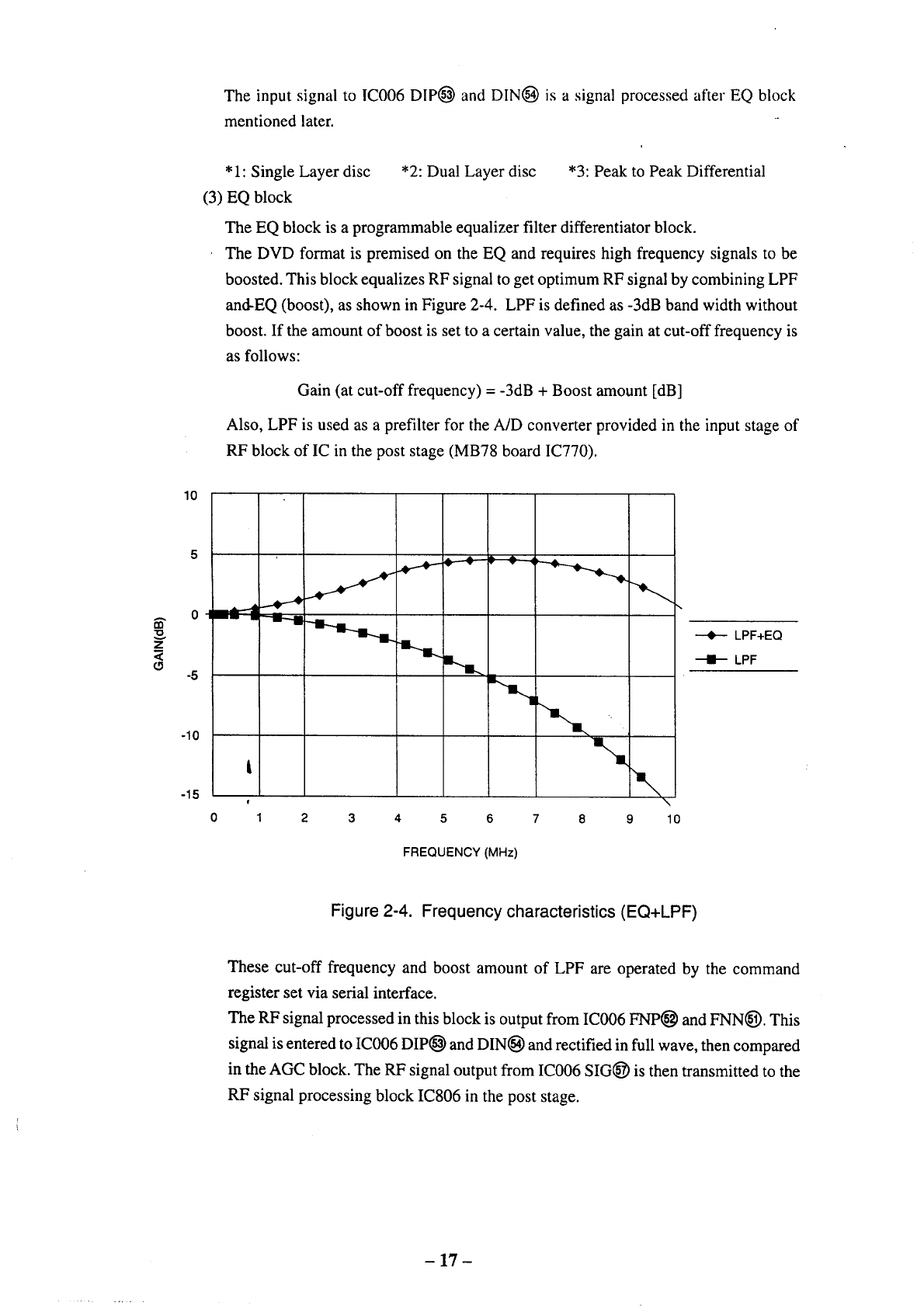
(3)EQblock
TheEQblockisaprogrammableequalizerfilterdifferentiatorblock.
TheDVDformatis premisedontheEQandrequireshighfrequencysignalstobe
boosted.ThisblockequalizesRFsignaltogetoptimumRFsignalbycombiningLPF
and-EQ(boost),asshownin Figure2-4. LPFisdefinedas-3dBbandwidthwithout
boost.If theamountofboostissettoacertainvalue,thegainatcut-offfrequencyis
asfollows:
Gain(atcut-offfrequency)= -3dB+ Boostamount[dB]
Also,LPFisusedasaprefilterfortheA/D converterprovidedintheinputstageof
RFblockof IC inthepoststage(MB78boardIC770).
wl
v
_z
10
-5
-10
-15
0
t
1 2 3456 7 8 9 10
FREQUENCY (MHz)
---e.--- LPF+EQ
--D-- LPF
Figure 2-4. Frequency characteristics (EQ+LPF)
These cut-off frequency and boost amount of LPF are operated by the command
register set via serial interface.
The RF signal processed in this block is output from IC006 FNP_ and FNN(_). This
signal is entered to IC006 DIP_ and DIN(_) and rectified in full wave, then compared
in the AGC block. The RF signal output from IC006 SIG(_ is then transmitted to the
RF signal processing block IC806 in the post stage.
- 17 -
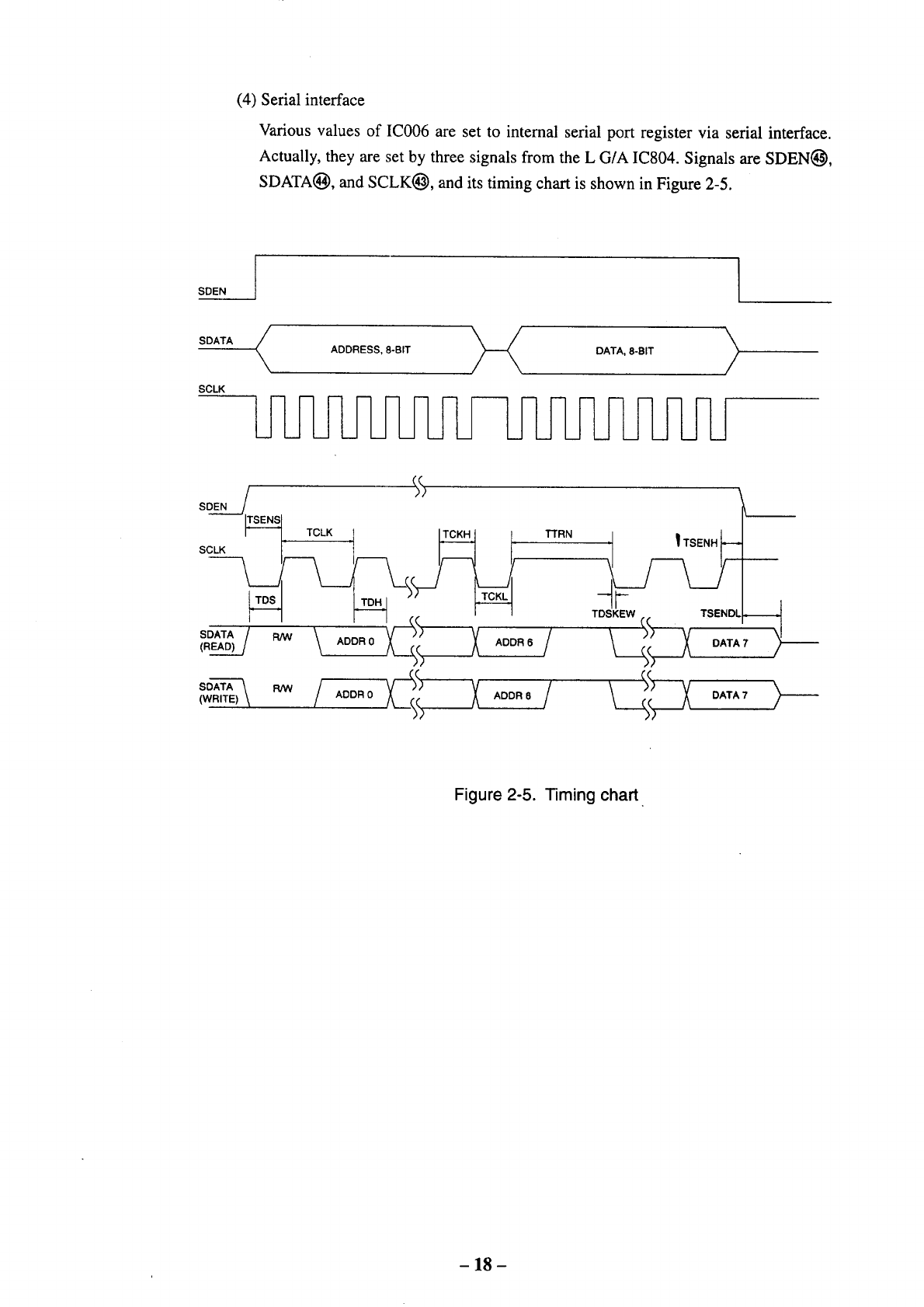
(4) Serial interface
Various values of IC006 are set to internal serial port register via serial interface.
Actually, they are set by three signals from the L G/A IC804. Signals are SDEN_,
SDATA_), and SCLK(_, and its timing chart is shown in Figure 2-5.
SDEN
SDATA (
SCLK LJ
ADDRESS, 8-BIT _DATA, 8-BIT )
SDEN
SCLK
SDATA /
(READ)/
SDATA \
(WRITE)
TCLK TTRN
ADDR0
ADDR0
Figure 2-5. Timing chart
- 18-
2-2. CD RF Front End
OPTICAL
BLOCK
rTK-47 board
_1 cNO01 -_
<
CXA,?.5550
CDRF TK-47 board
To MB-78 board
IC.806 ARP
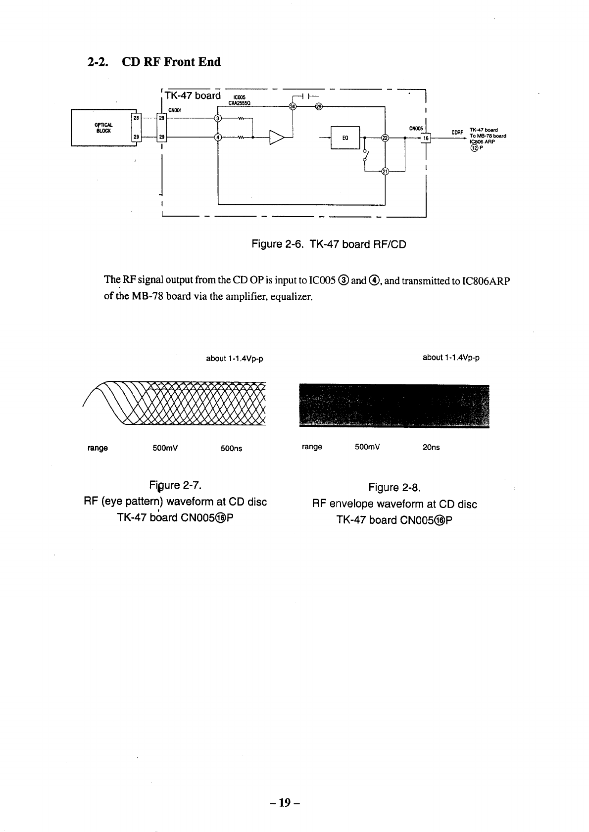
Figure 2-6. TK-47 board RF/CD
The RF signal output from the CD OP is input to IC005 (_) and (_), and transmitted to IC806ARP
of the MB-78 board via the amplifier, equalizer.
about 1-1.4Vp-p about 1-1.4Vp-p
range 500mY 500ns range 500mY 20ns
Fi0ure 2-7.
RF (eye pattern) waveform at CD disc
I
TK-47 board CN005(_P
Figure 2-8.
RF envelope waveform at CD disc
TK-47 board CN005(_P
- 19 -
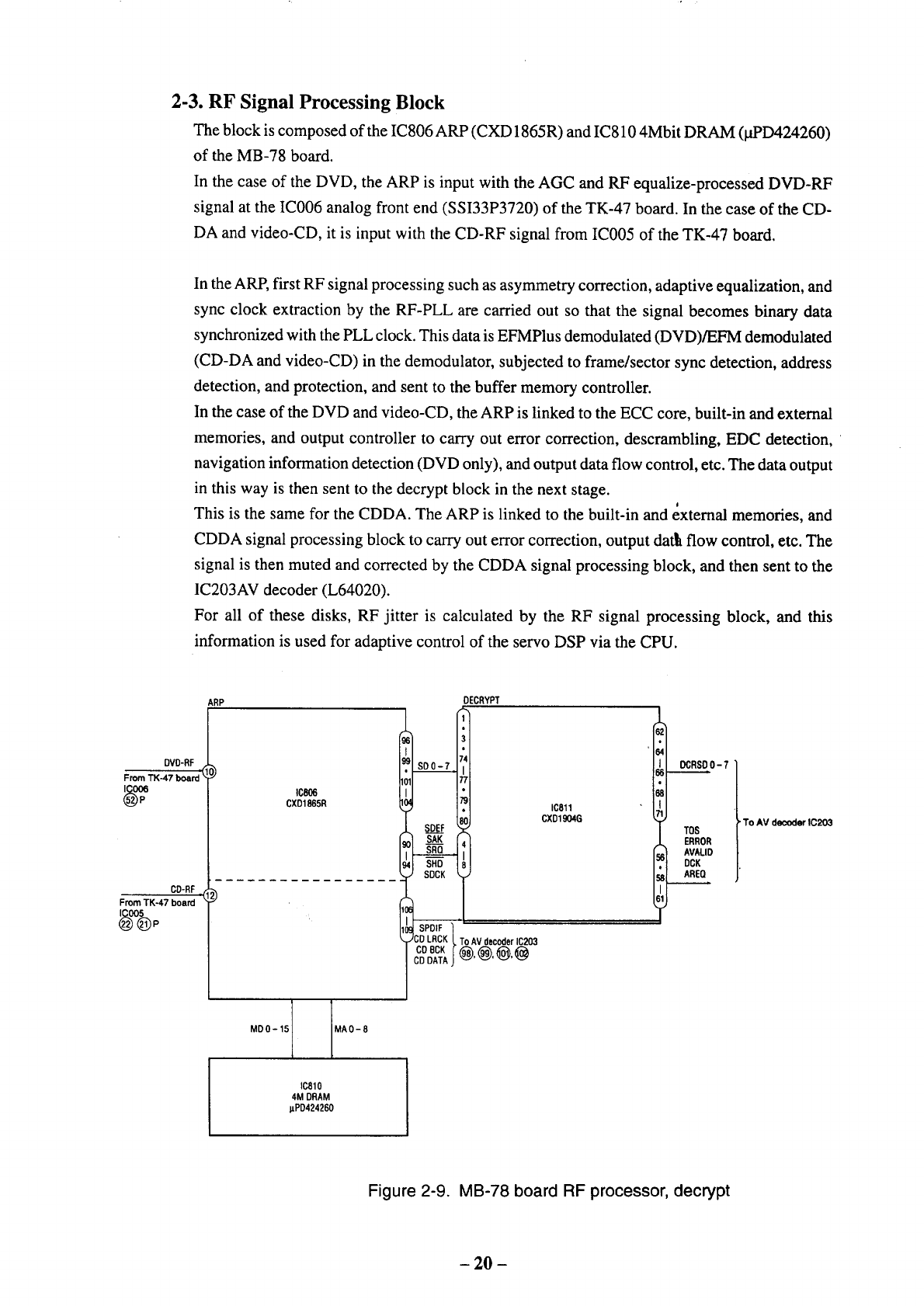
2-3. RF Signal Processing Block
The block is composed of the IC806 ARP (CXD 1865R) and IC810 4Mbit DRAM (I.tPD424260)
of the MB-78 board.
In the case of the DVD, the ARP is input with the AGC and RF equalize-processed DVD-RF
signal at the IC006 analog front end (SSI33P3720) of the TK-47 board. In the case of the CD-
DA and video-CD, it is input with the CD-RF signal from IC005 of the TK-47 board.
In the ARP, first RF signal processing such as asymmetry correction, adaptive equalization, and
sync clock extraction by the RF-PLL are carried out so that the signal becomes binary data
synchronized with the PLL clock. This data is EFMPlus demodulated (DVD)/EFM demodulated
(CD-DA and video-CD) in the demodulator, subjected to frame/sector sync detection, address
detection, and protection, and sent to the buffer memory controller.
In the case of the DVD and video-CD, the ARP is linked to the ECC core, built-in and external
memories, and output controller to carry out error correction, descrambling, EDC detection,
navigation information detection (DVD only), and output data flow control, etc. The data output
in this way is then sent to the decrypt block in the next stage.
J
This is the same for the CDDA. The ARP is linked to the built-in and external memories, and
CDDA signal processing block to carry out error correction, output datll flow control, etc. The
signal is then muted and corrected by the CDDA signal processing block, and then sent to the
IC203AV decoder (L64020).
For all of these disks, RF jitter is calculated by the RF signal processing block, and this
information is used for adaptive control of the servo DSP via the CPU.
ARP DECRYPT
DVD-RF (
From TK-47 boa_
CD-RF.(
From TK-47 boa_
IC806
CXD1865R
_O LRCK(. To AV decoder IC203
CD DATA)_J, _-.-, ,_J, _-._
IC811
CXD1904G
OCRSD0 - 7
TOS
ERROR
AVALID
DCK
AREQ
' To AV decoder IC203
MDO-15 MAO-8
IC810
4M DRAM
pPD424260
Figure 2-9. MB-78 board RF processor, decrypt
- 20 -
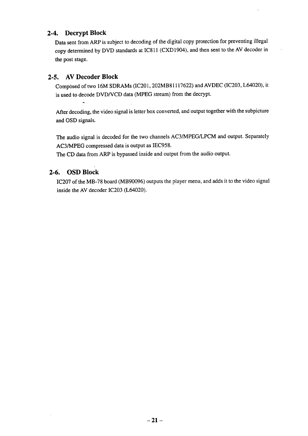
2-4. Decrypt Block
Data sent from ARP is subject to decoding of the digital copy protection for preventing illegal
copy determined by DVD standards at ICS11 (CXD1904), and then sent to the AV decoder in
the post stage.
2-5. AV Decoder Block
Comp0sed of two 16M SDRAMs (IC201,202MB 81117622) and AVDEC (IC203, L64020), it
is used to decode DVD/VCD data (MPEG stream) from the decrypt.
After decoding, the video signal is letter box converted, and output together with the subpicture
and OSD signals.
The audio signal is decoded for the two channels AC3/MPEG/LPCM and output. Separately
AC3/MPEG compressed data is output as IEC958.
The CD data from ARP is bypassed inside and output from the audio output.
2-6. OSD Block
IC207 of the MB-78 board (MB90096) outputs the player menu, and adds it to the video signal
inside the AV decoder IC203 (L64020).
- 21 -
IC203 AV Decoder
(L64020)
FromIC807 ('CG--'_'O
SGA , _SO
CXD08747 ' L SCLKO
IC207
MB90096
OSO
FromIC806ARP --
DCRSD 0-7
TOS
ERROR
AVALID
DCK
AREQ
CDLRCK
CDBCK
CDDATA
SPDIF
YC0-7
-- To IC251 DNR
AU-197
0353
iC351_C°axial °utptzt ] 0joltal
GPIF32T Ioutput
IC102 OIR (To LC8905t)
AVDATA
AV LRCK
AVBCK
tTo IC101 MGA (2cll signal)
IC201
IC202
16M SOP,AM
AVIO0-15
Figure 2-10. AV Decoder, OSD
- 22 -
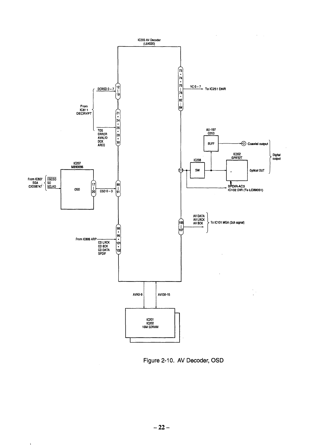
2-7. DNR, Video Encoder Blocks
The video data from the AV decoder is sent to IC251, DNR (CXD1854), subjected to video
noise reduction, and sent to the IC252 video encoder CXD1914 in the post stage. The video
data is converted to NTSC/PAL video signal (Color difference signal/S-Y, S-C/composite) here.
IC252
IC2510NR VIDEO ENCORDER
CXD1854 CXD 1914
From vr
IC203 '"
AV Decoder
C0-7
YO-7
R-Y 1
For color difference output
Y
J
B-Y
VIDEOC
ForS terminal
VIDEOY
VIDEOV Compositevideo
Figure 2-11. DNR video encoder
Signals are output externally after passing through the 75 _ driver.
- 23 -
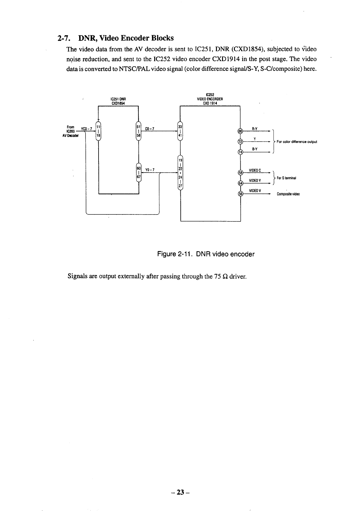
2-8. Clock Generator Block
The IC209 CXD8696PLL IC generates 27 MHz, and using this as the master clock, generates
the system clock for audio decoding.
System Clock 384fs 768fs
CD/VCD 16.9344 MHz 33.8688 MHz
DVD 18.4320 MHz 36.8640 MHz
IC209 IC206 SN74ABT12608
PLL
CXD8696 BUFF
X210
27MHz
)
)
1(;205 SN74ABT12608
BUFF
27.0000MHz
)7_Sfs
384fs
=
33.8688MHz
Figure 2-12. Clock generator
- 24 -
2-9. AC-3 Decoder Block
FromL_A (tC_4) 8s'r
SCKG2
SOG2From_11c8o5);
I
AV_II
OR LRCK (
M G/A (IC101)
CXO 87460
6STC
$062C
AC-3
DECODER
(IC_04)
M886342
AC3__K
AC;_LRCK
/2
AC3_DATA F
AC3_OATAR
AC3.OATA C
/3
DD_BCK l
DO_LRCK
DD_OATA F 1
256KS_
N341256
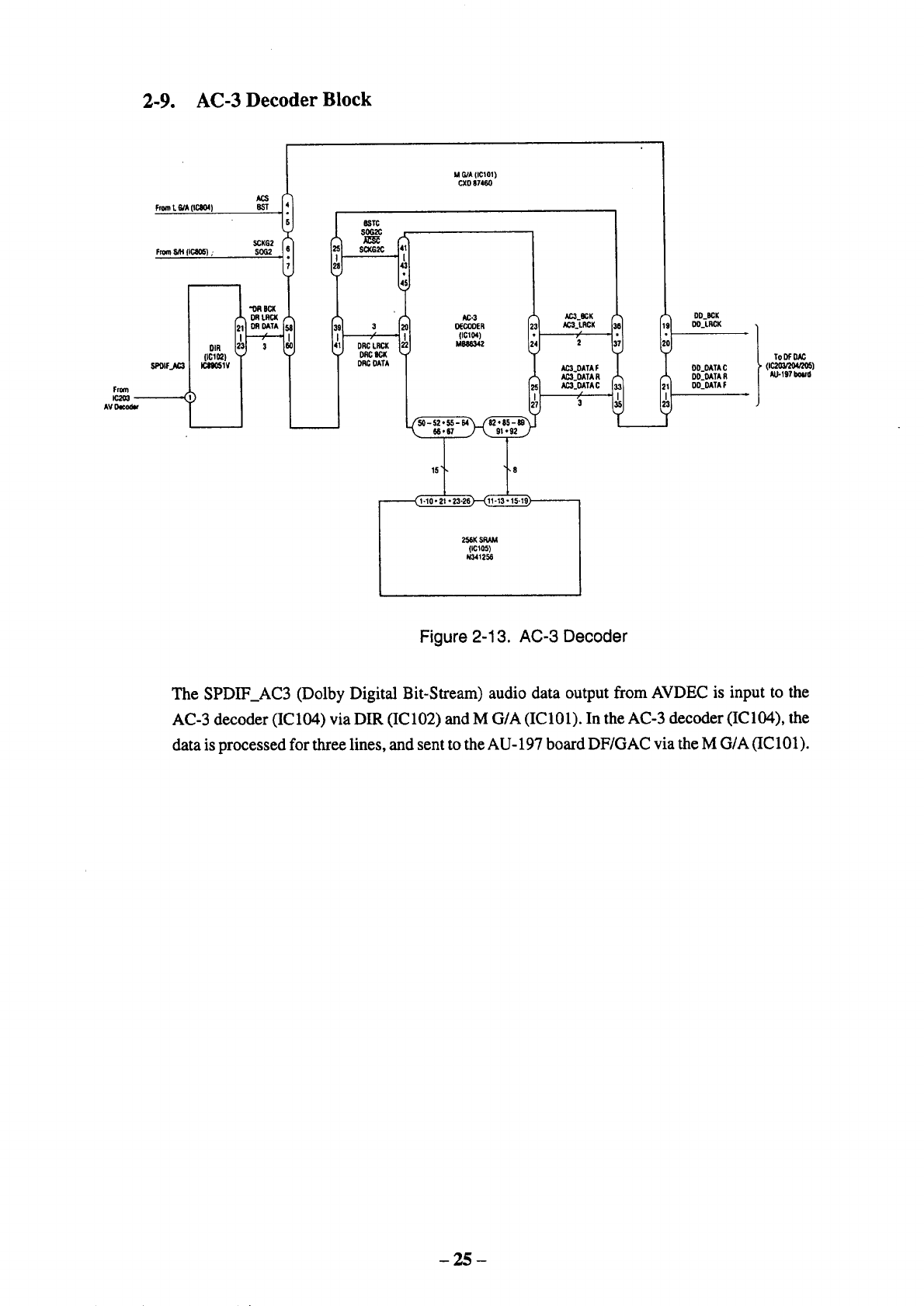
Figure 2-13. AC-3 Decoder
The SPDIF_AC3 (Dolby Digital Bit-Stream) audio data output from AVDEC is input to the
AC-3 decoder (IC104) via DIR (IC102) and M G/A (IC101). In the AC-3 decoder (IC104), the
data is processed for three lines, and sent to the AU- 197 board DF/GAC via the M G/A (IC 101).
- 25 -
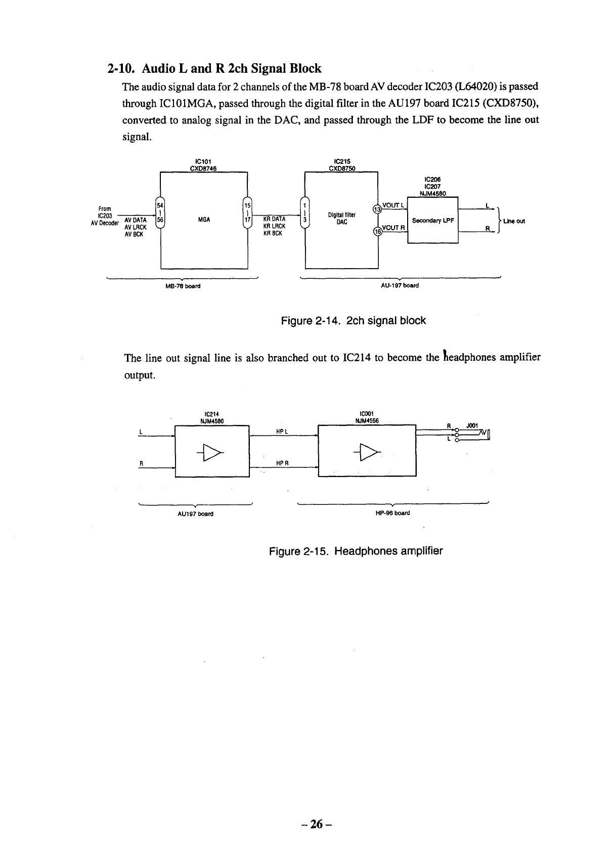
2-10. Audio L and R 2ch Signal Block
The audio signal data for 2channels of the MB-78 board AV decoder IC203 (L64020) is passed
through IC101MGA, passed through the digital filter in the AU197 board IC215 (CXD8750),
converted to analog signal in the DAC, and passed through the LDF to become the line out
signal.
From
IC203
AVDecoder AVDATA
AVLRCK
AVBCK
IC101 IC215
CXD8746 CXD8750
MGA KRDATA
KRLRCK
KR BCK
Digitalfilter
DAC
IC206
IC207
NJM4580
Secondary LPF Line oul
MB-78 board ""AU-197 board
Figure 2-14. 2ch signal block
The line out signal line is also branched out to IC214 to become the _eadphones amplifier
output.
L
R
IC214 IC001
NJM4580 NJM4556
-E> .,. -E>
R JO01
Y
AU197 board
_r
HP-96 board
Figure 2-15. Headphones amplifier
- 26 -
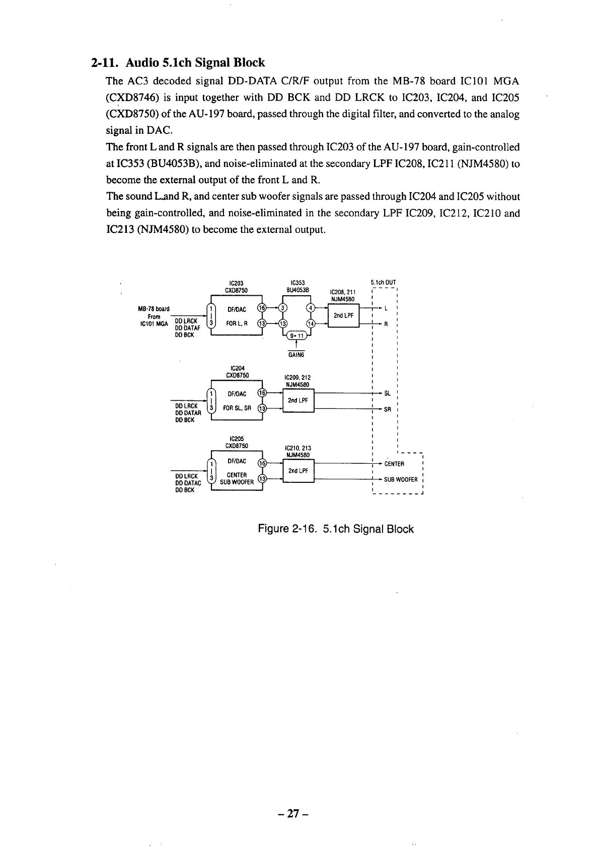
2-11. Audio 5.1ch Signal Block
The AC3 decoded signal DD-DATA C/R/F output from the MB-78 board IC101 MGA
(CXD8746) is input together with DD BCK and DD LRCK to IC203, IC204, and IC205
(CXD8750) of the AU-197 board, passed through the digital filter, and converted to the analog
signal in DAC.
The front L and Rsignals are then passed through IC203 of the AU- 197 board, gain-controlled
at IC353 (BU4053B), and noise-eliminated at the secondary LPF IC208, IC211 (NJM4580) to
become the external output of the front L and R.
The sound Land R, and center sub woofer signals are passed through IC204 and IC205 without
being gain-controlled, and noise-eliminated in the secondary LPF IC209, IC212, IC210 and
IC213 (NJM4580) to become the external output.
IC203 5.1ch OUT
CXD8750
MB-78board _DF/DAC
From DD LRCK =FOR L,R
IC101MGA DDbATAF
DDBCK
IC204
CXD8750
,_DF/DAC
DD LRCK FOR SL, SR
DO DATAR
DO BCK
IC205
CXD8750
___ DF/DAC
DD LRCK CENTER
DD DATAC SUB WOOFER
DO 8CK
IC353
BU4053B IC208, 211
GAIN6
---L
_R
IC209,212
, - SL-SR
IC210,213
_CENTER:
I
I
'SUBWOOFER I
I I
I_J
Figure 2-16. 5.1ch Signal Block
- 27 -
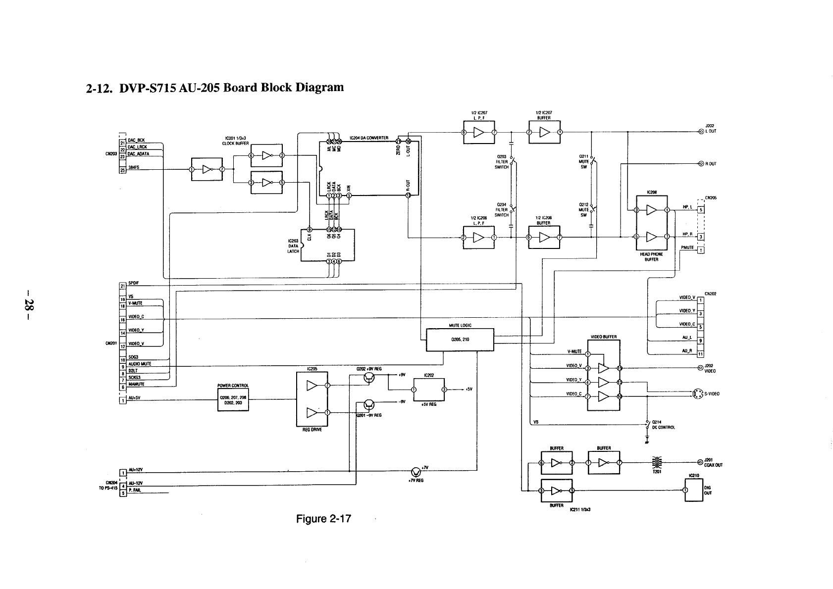
2-12. DVP-S715 AU-205 Board Block Diagram
I
i
7_
OAC BCK
DA,C LRCK
CN203 OAC AOATA
IF
CN201 SOG3
AUDIOMUTE
D2LT
SCKG3
_AU*SV
_E01 1/3x3 IC204 DA CONVERTER _i
CLOCK BUFFER
kATe
1/2 _CL_I7 1/2 IC207
L P, F BUFFER
0203
FILTER
SWITCH
POWERCONTROL
MUTE LOGIC
0205, 210
I
IC_85 Q2_ *W REG
_ ÷5V
---_ --W _EV REG
_1 .-_ REO
REG DRIVE
Q204
FILTER
SWITCH
1/2 1C206
L,P,F
['1--_AU*E2V
i'
CRY04 _ _1_
TO_-415 p. FAIL
Figure 2-17
1
t/2 IC206
BUFFER
0211
MUTE
SW
0212
MUTE
SW
VIDEO BUFFER
V_OEO V,
VIDEO Y
VIDEOIC
vs
J202
(_) L OUT
i (_ R OUT
IC208 HP, L ;" _ ,CN205
PMUTE I,
CR202
VIDEO V
VIOEO_YAuL
J20_
_) VIDEO
[© S-V,D_O
Q214
OCCONTROL
BUFFER BLB:FER
J_F
©c_
_tO
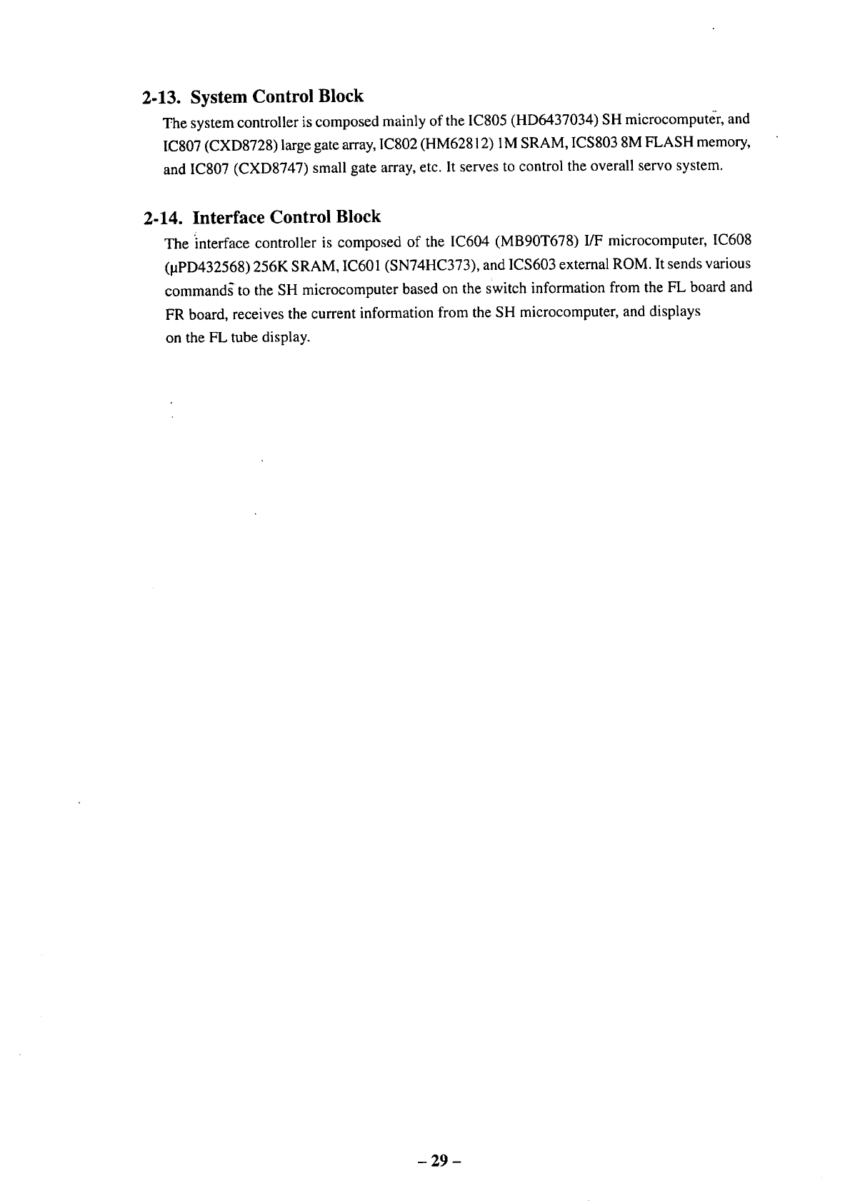
2-13. System Control Block
The system controller is composed mainly of the IC805 (HD6437034) SH microcomputer, and
IC807 (CXD8728) large gate array,1C802 (HM62812) 1M SRAM, ICS803 8M FLASH memory,
and IC807 (CXD8747) small gate array, etc. It serves to control the overall servo system.
2-14. Interface Control Block
The 'interface controller is composed of the IC604 (MBg0T678) I/F microcomputer, IC608
(_PD432568) 256K SRAM, IC601 (SN74HC373), and ICS603 external ROM. It sends various
commands to the SH microcomputer based on the switch information from the FL board and
FR board, receives the current information from the SH microcomputer, and displays
on the FL tube display.
- 29 -

SH
Servo Block
I
AC3 i_
Block
J
ARPBlock i_
J
SerialDevise i_
I/0
SA[0:19]
4SD[0:15]
Vcc=5V
Address
DATA
10805
HD 6437034 RD
WR
System Control CSO
Drive Control CSl
CS6
WAIT
1:3 r'_
XX
r,-- tY-
t
IRQO
IRQ6
IRQ7
IRQ3
IRQ2
TxDO
TxD1
SCK1
SIC1
SIC2
I
SOG1]
Out put
Iv
T
Hsync (from 0XD1914)
AdvancedHSYNC
• (for OSD, DNR,AVDEC)
1(3803 Vcc=5v
ROM(Flash)SMbit
IC802 Vcc=5v
RAM (1Mbit)
HM628128
._k ,LL A
r_ 00 ,,'-
_<_1_
T
•--Lo L JI
{9O T
____ INT&WAIT
co Control
_RxDs
MPX
Expansion
I/O 10804
LGA
CXD8728
T
LGA
=.-
o
fO
Q.
Address Bus
Decode Controll_
Device I
ChipSelectL
INT Control-_
WAlT C:nxt_:ll,
Gro.up.2
Chip_elect
r_
Tx DOSel -_
Rx DOSel
n
Serial [-
Gp3,4 /
CONTROLL
SOG2PS
_" 13 SCKG2PS
_- _ AVCK
=_J3
G,Oir
IWRn
IRDn
SDSPWRn
SDSPRDn
ARPCSn
DCRCSn
AVCSn
4 ARPINT
DCRINT
4ARPWIn
4DCRWrn
AVWTn
4Group2RxOs
4
IFSO
DBSO
IFSI
•DBSI
_CKG3
SOG3
SCKG4
SOG4
SCKG4n(DCLK)
IC 506
Servo DSP
CXD8730
dir&G Control
BusBuffer
(SGA)
J
J
J
J
JPSEL I
101
IC203~205
II DAC
oxo8 2
10102
DIR
LC89051V
o_,
Vcc=5V
,'-" I--
C3 z
_cE
O'3 (:3
00
j
IC806 Vcc=3.3V
ARP
CXD1865
t d, Ai, d
P
I
_._
I
_1_1 _/_1
AC3 Dec VEnc >
MB8-6342I C_D_9_4Q/
;°J
Serial
Gpl "
Serial
Gp2
,coo6_ _
SSl o_ IC251 (n
(SS133P3720) DNR
I_: ,,z, CXD1854Q
(::3 t-'t
IC811 Vcc=5V
DECRIPT
CXD1904
_--I._. _ _ _z_
o,1o "__
;
i
d
IC 203
AV_DEC
L64020
"To Expansion
I/O XI_FBSY
(Handshake)
IFSO=
IFSI_
10604
MB90T678
I/FCON SlO
Ch_n
SlO SO
Ch m SCLK
- FLCS
Sl_m FLCS
SO_m
CN802
Diagnostic
IConnector
DBSO..1 Rxl3
DBSI"t Tx[)
Expansion_ DIAGN I
I/O
II
03
EEPROM
BA9020F
LU
1.1.1
Vcc=3.3V
,,=:
1
IC215
DAC
CXD8750
10207 IC101
MB90096A 11 pPD16311
OSD FL_ConI
SlSCLKCGGS SISCLKFLCS
10807
0XD8747
y.
Serial Gp4
)kY
Serial Gp3
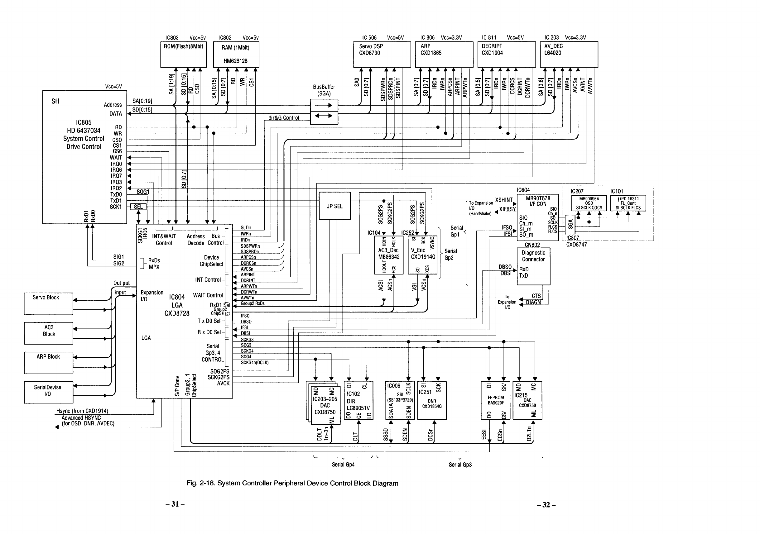
Fig. 2-18. System Controller Peripheral Device Control Block Diagram
- 31 - -32-
3. SERVO BLOCK 3-2. Servo Operation at DVD Play
3-1. General Description of Servo Circuits
3-1-1. Optical Pickup Control
Dedicated optical pickups for DVD and for CD and video CD are provided. The focus and
tracking servo gains are automatically adjusted for every disc loading so that the gains are
constant for every disc to be played.
3-1-2. Sled Control
Two pickups for DVD and CD/video CD are placed on the same sled, and the position is
controlled with one sled motor. The sled motor is attached with a speed detector utilizing
the Hall element, and a sled speed fluctuation due to mechanical load variations is minimized
by applying the speed servo control (feedback control).
The sled motor used is a DC motor with a brush.
The servo system circuit is used for both DVD and CD.
3-1-3. Spindle Control
One 3-phase brushless motor controls all disc rotations. The rotation detection pulses (FG:
Frequency Generator) utilizing the Hall element are used for control.
3-1-4. Tilt Control
The optical pickup is controlled so that the optical axis is perpendicular to the disc; when
DVD is played, it is controlled so that the time axis variation (jitter) of RF signal becomes
minimum.
At the start of DVD play (before RF signal is output), optical sensor detects the tilt angle of
disc and the optical pickup is controlled so that the optical axis is perpendicular to the disc.
The servo system circuit is used for both DVD and CD. At DVD, it always performs tilt
operation, but at CD, it operates only during start-up and stops at the tilt position during
playback.
3-1-5. Disc Loading and Chucking
One DC motor drives the tray in-out motions, and chucking of disc.
3-1-6. Disc Judgment
The presence of a disk is judged from the spindle motor spinning start-up time.
Also, the disc size (12cm or 8cm) is judged from the spindle motor speed-up time and disc
data.
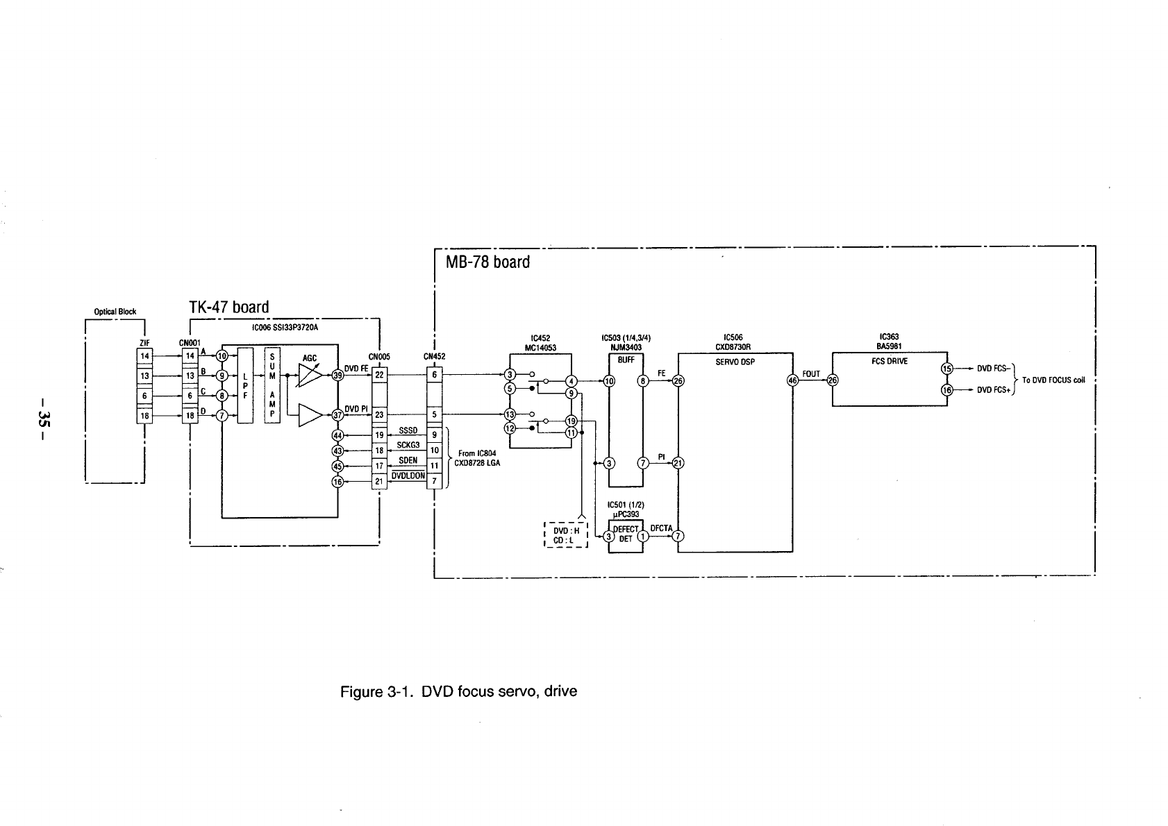
3-2-1. Optical Pickup Control
(1) DVD focus servo
The focus error signal output from the optical pickup for DVD (hereinafter referred to
as optical pickup) is entered to the TK-47 board IC006: SSI33P3720A A to D ((_ to
(_)P).
The balance amount and offset amount of the focus error signal is set by IC805 (CPU)
via IC804 of the MB-78 board using the internal register of IC006.
The focus error signal is generated at TK-47 board IC006, amplified, and output from
the FE terminal (_p).
The IC006 FOCUS error (DVD FE) signal is input to the MB-78 board via the flexible
flat cable.
The error signal is switched according to whether the disc type is DVD or CD by the
switch IC452, its signal level is adjusted by IC503 (OP amplifier (_), (_), (_p), and it is
input to the servo DSP IC506 (CXD8730R) _p.
-33 - - 34 -
I
Ln
I
Optical Block
r
i
i
i
]
ZIF
TK-47 board
IC006 SS133P3720A
CNO01 I
MB-78 board
i
I
' tC452
I MC14053
i
I
CNO05 CN452 r I
_-- _ ,__
_sso7] '._---_--_
s_,,_,<l ,,o,.,cBo,,' ' I
' I__'__ l
|
iC503 (1/4,3/4)
NJM3403
FE
IC501 1/2
IC506
CXD8730R
SERVODSP
IC363
BA5981
FCSDRtVE
DVD FCS--_ To DVD FOCUScoil
DVDFCS+_
Figure 3-1. DVD focus servo, drive
The IC506 Servo DSP: CXD8730 on MB-78 board provides the following control in
the focus servo system.
(a) Focus search
The optical pickup lens is moved toward a disc to turn on the focus servo.
The focus servo loop is turned on when the PI (Pull IN) signal (used for FOK:
Focus OK) exceeds the specification (Vc +0.25V) and the FE signal zero-crossing
is detected.
(b) Focus gain adjustment
The gain of digital filter in the IC506 is automatically adjusted so that the focus
servo loop gain becomes optimum.
Consequently, the optimum gain for each disc to be played can be attained, besides
correction of gain variations in focus actuator (coil) and optical pickup sensor
(photodiode for focusing).
(c) Focus bias adjustment
The focus bias is added to the focus servo filter so as to mi_mize the jitter.
Consequently, a variation of optical pickup and disc can be automatically corrected.
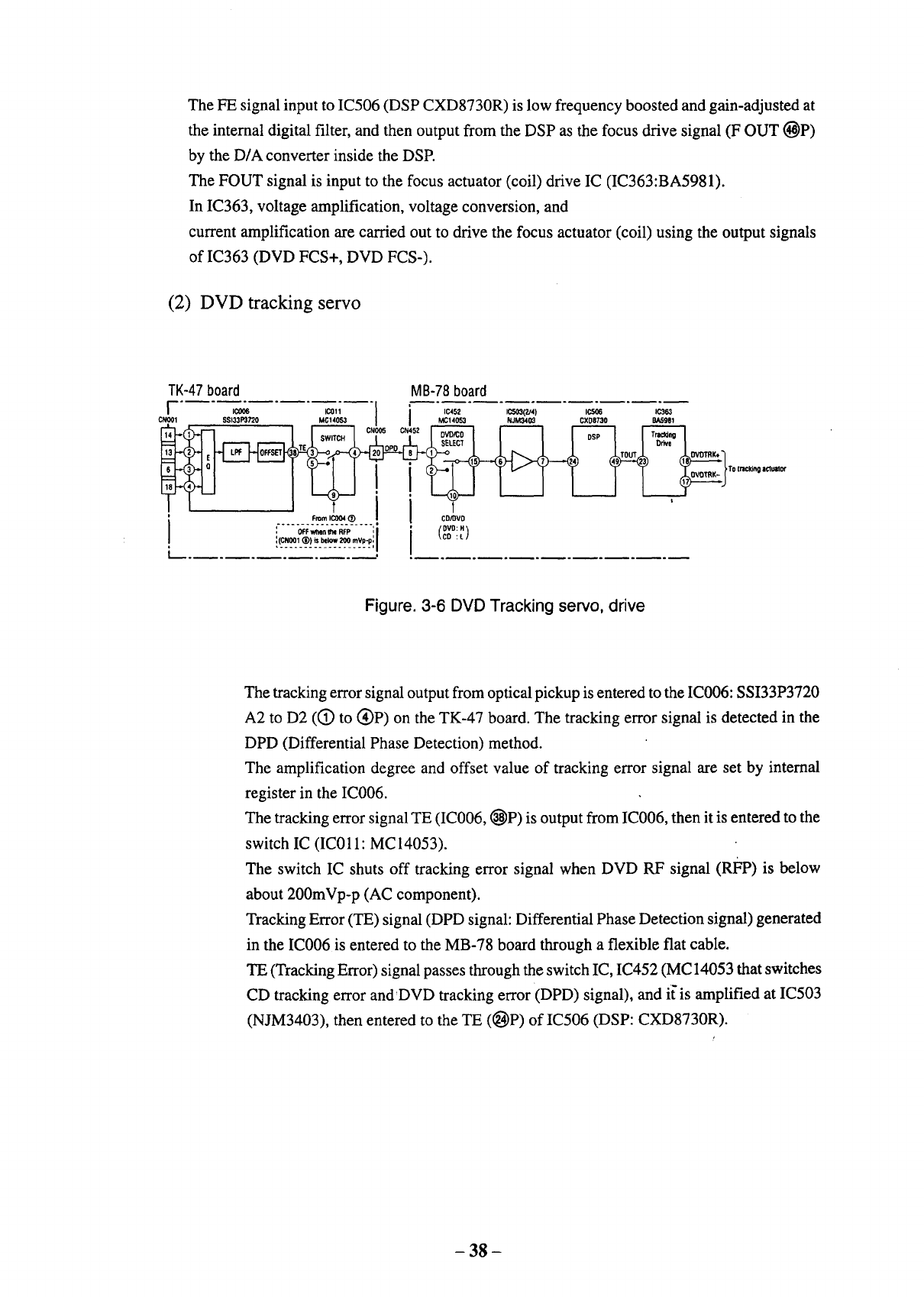
(d) Focus jump
Operation carried out when playing back the DVD dual layer disc to perform
focusing jump between layer 0 (PU side layer) and layer 1 (far end layer).
First the servo loop is turned off, the kick voltage is supplied to the focus actuator,
and the focus is jumped to the targeted layer. As the focus approaches the desired
layer, the FE signal appears. The voltage of this signal is monitored, the deceleration
pulse is generated, and the focus servo is turned ON again after focusing.
These operations from the start to end of jumping are all performed inside the
DSP.
- 36 -
,'topped
CNI_OOmV: : _ i 2ms/div
I_. 10:1 _(2ms_'_v)
:!I' i
:T
...........................ii...................!........;..................................
! :
: !
i
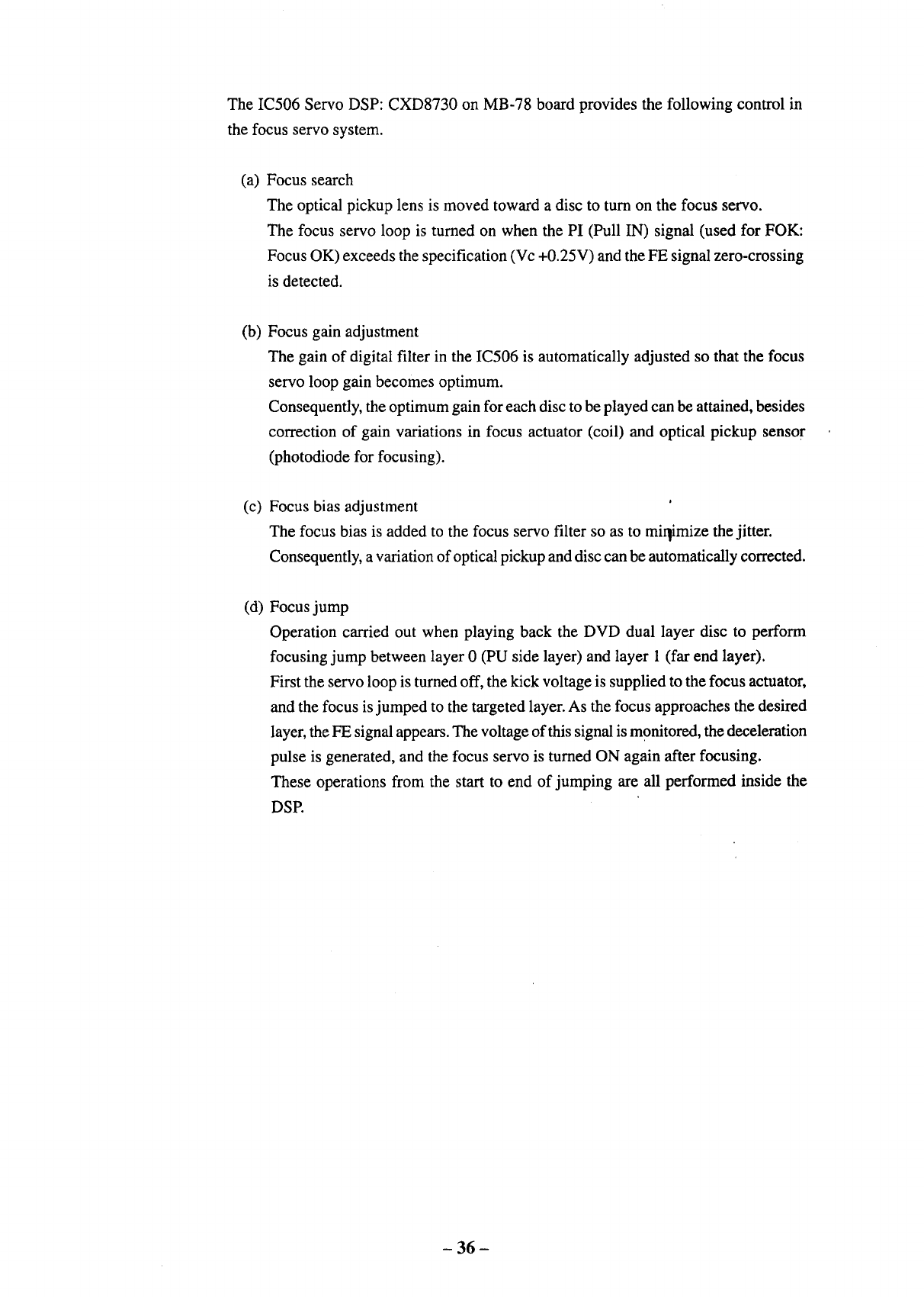
Figure 3-2. Example of S-shape
waveform for the DVD disc
(single layer) MB-78 board
CN303 (_P
;topped
CHI=5_mV: _ + : _$/_v
: : : f i _2QOk875
...... ]....... ]...... ]......... i ........ ??......... ]......... !......... i ........ [........
i: ;i '* i_}i
'!i .... ............il_.............................ii..............
i
......................................................... :......... ! ......... :...................
i :
Figure 3-3. Example of S-shape
waveform for the DVD disc
(dual layer) MB-78 board
CN303 (_)P
FOK
PI
FE
FOUT
BUSY
Figure 3-4. Focus jump waveform
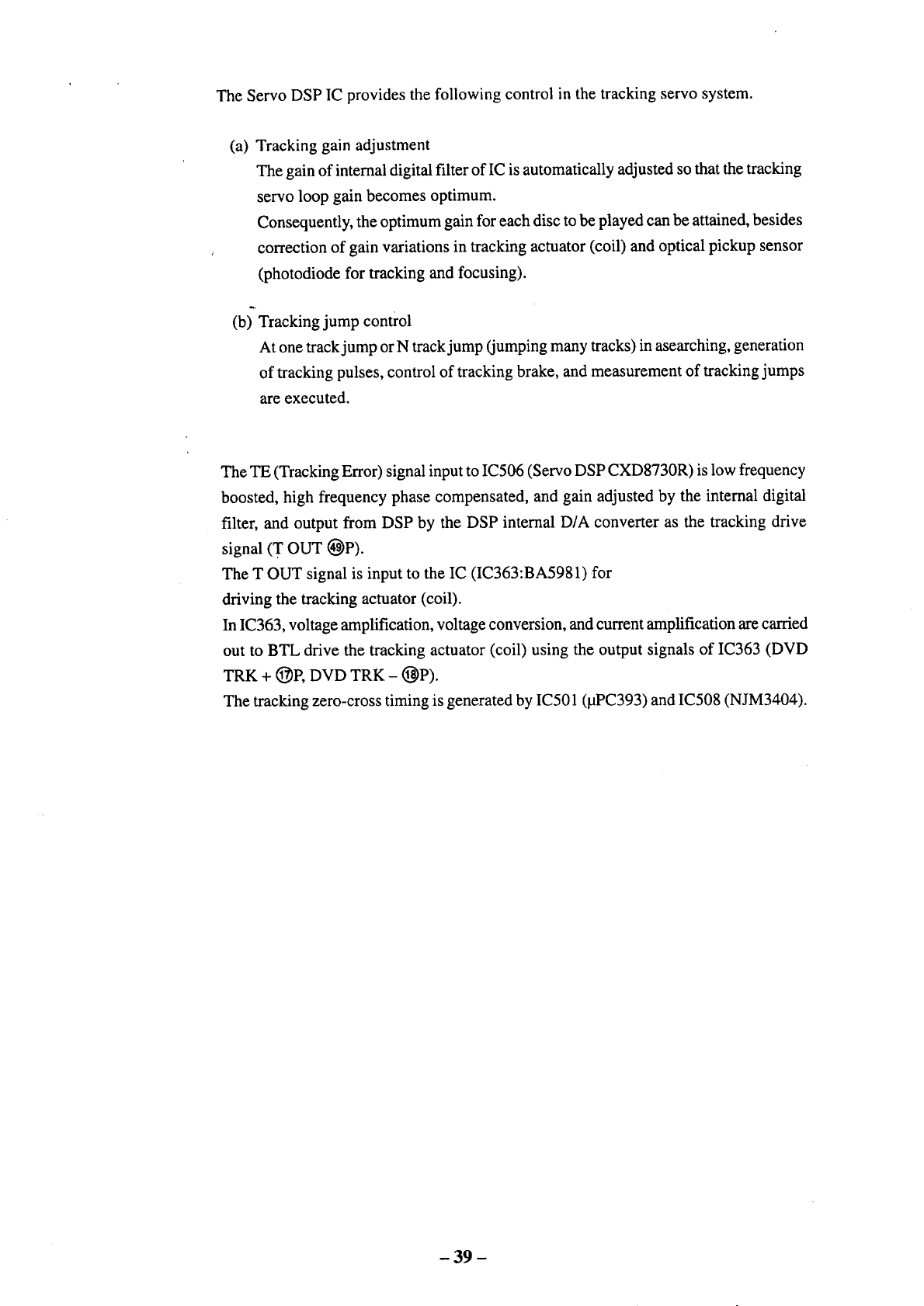
M_IRR............
Tzc]
................ .ii, DFCTS
[
OSPCORE IBUSY
I FON
___ _ I,ou,
PWM l _ SLOFS
fTiOFS
Figure 3-5. Example of S-shape
waveform for MB-78 board
CXD8730R (Layer) MB-78
board CN303 (_)P
-3? -
The FE signal input to IC506 (DSP CXD8730R) is low frequency boosted and gain-adjusted at
the internal digital filter, and then output from the DSP as the focus drive signal (F OUT _)P)
by the D/A converter inside the DSP.
The FOUT signal is input to the focus actuator (coil) drive IC (IC363:BA5981).
In IC363, voltage amplification, voltage conversion, and
current amplification are carried out to drive the focus actuator (coil) using the output signals
of IC363 (DVD FCS+, DVD FCS-).
(2) DVD tracking servo
TK-47board MB-78 board
ICG06 IC011 i Ic452 IC503(2/4) IC506 IC363
CNO01 8S133P3720 MC14053 IMC14053 NJM3403 CXD8730 BA5981
DPD TOUT D_I d
'....... F_'*pLc_..__.. _ Ict;iovo
', OFFwf'mnI_ RFP ', _ (OVO: H_
!(.c__ooL._!_ .._,y.vp.-.pl I_co:_/
To tr_kino actuator
Figure. 3-6 DVD Tracking servo, drive
The tracking error signal output from optical pickup is entered to the IC006:SSI33P3720
A2 to D2 (O to (_)P) on the TK-47 board. The tracking error signal is detected in the
DPD (Differential Phase Detection) method.
The amplification degree and offset value of tracking error signal are set by internal
register in the IC006.
The tracking error signal TE (IC006, _P) is output from IC006, then it is entered to the
switch IC (IC011: MC 14053).
The switch IC shuts off tracking error signal when DVD RF signal (RFP) is below
about 200mVp-p (AC component).
Tracking Error (TE) signal (DPD signal: Differential Phase Detection signal) generated
in the IC006 is entered to the MB-78 board through a flexible fiat cable.
TE (Tracking Error) signal passes through the switch IC, IC452 (MC14053 that switches
CD tracking error andDVD tracking error (DPD) signal), and it"is amplified at IC503
(NJM3403), then entered to the TE (_)P) of IC506 (DSP: CXD8730R).
!
- 38 -
The Servo DSP IC provides the following control in the tracking servo system.
(a) Tracking gain adjustment
The gain of intemal digital filter of IC is automatically adjusted so that the tracking
servo loop gain becomes optimum.
Consequently, the optimum gain for each disc to be played can be attained, besides
correction of gain variations in tracking actuator (coil) and optical pickup sensor
(photodiode for tracking and focusing).
(b) Tracking jump control
At one track jump or N track jump (jumping many tracks) in asearching, generation
of tracking pulses, control of tracking brake, and measurement of tracking jumps
are executed.
The TE (Tracking Error) signal input to IC506 (Servo DSP CXD8730R) is low frequency
boosted, high frequency phase compensated, and gain adjusted by the internal digital
filter, and output from DSP by the DSP internal D/A converter as the tracking drive
signal (T OUT _P).
The T OUT signal is input to the IC (IC363:BA5981) for
driving the tracking actuator (coil).
In IC363, voltage amplification, voltage conversion, and current amplification are carded
out to BTL drive the tracking actuator (coil) using the output signals of IC363 (DVD
TRK + _)P, DVD TRK - (_P).
The tracking zero-cross timing is generated by IC501 (1JPC393) and IC508 (NJM3404).
- 39 -
_.t,opped
CHI=500mV
DC 10:1
_" 5m:S_/div r
:: (Sm$t'div)
2NORM:20_kS/S
t
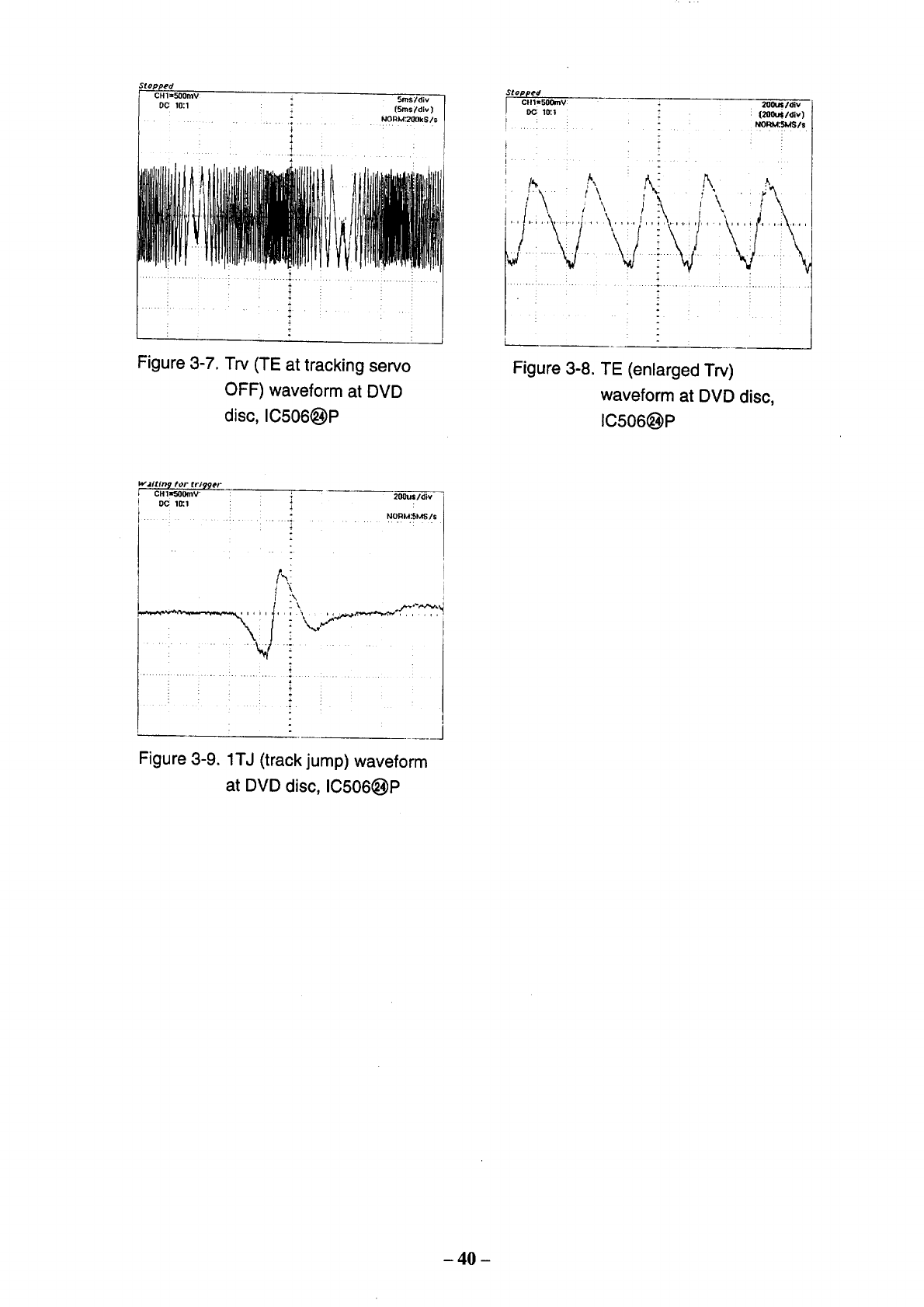
Figure 3-7. Trv (TE at tracking servo
OFF) waveform at DVD
disc, IC506(_)P
Stopped
CHlt506mV: 200us/dfv
• i (200_/div)
MORM:.SMS/$
Figure 3-8. TE (enlarged Try)
waveform at DVD disc,
IC506(_)P
Figure 3-9. 1TJ (track jump) waveform
at DVD disc, IC506_)P
-40 -
3-2-2. Sled control
LBF HPF
=_ Tracking block _,
IC506
CXD8730R
SLOFS
SOUT
SDCNT
HYCNT
IC302
LA6527N
,_ledDrive
,(
,(
,(
.(
FromFG-43 board,
IC501, IC502
I
I Feedback speed I
II control by Hall element j
Figure 3-10. DVD Sled control
' SLDMT _" To sled motor
_J
(1) Sled control during playing
During disc playing, namely, when the focus servo and tracking servo are turned on,
the sled servo controls the sled motor so that an objective lens of optical pickup positions
always in the center of movable range of tracking actuator.
The error signal of the sled servo is obtained by amplifying the low frequency components
of TE by the digital filter in the DSE Consequently, it cannot be observed externally.
Th[ error signal generated internally is output from SOUT ((_)P)) via the digital low
pass filter, and input to the sled driver IC302 (_P).
Thh sled driver carries out sled speed control constantly, and adds the SOUT voltage to
the control loop.
The Servo DSP IC506 CXD8730R carries out the following controls in the sled servo
block.
(a) Sled error signal generation
Carries out tracking error TE processing to generate the sled error signal.
(b) Sled error amplification
Amplifies the sled error signal by the LPF (Low Pass Filter) composed of the
digital filter and amplifier.
(c) Sled error ON/OFF
Tums ON the sled servo during normal playback, and turns it OFF when the
tracking servo is OFF when playback starts, during search, etc.
- 41 -
The sled error signal is passed through the digital filter in IC506 (DSP), and output
from the DSP as the SOUT ((_)P) signal from the D/A converter.
The SOUT signal is input to DVI ((_P) of the sled drive IC (IC302:LA6527N).
The sled drive IC incorporates a speed (motor rotation speed) feed back control using
the Hall element.
There are two speed detection Hall elements (HA, HB). The detection output is obtained
from the sled motor board (FG-43 board) as the differential output of (HA+, HA-)
(HB+, HB-).
The sled drive IC detects the inclination of the Hall element output waveform during
sled motor rotation (differential value near the zero cross) to form the speed feedback.
In the sled drive IC, after the sled error signal is converted to the sled motor rotation
speed signal, the voltage and current are amplified, and the sled (d.c.) motor is driven
by the output signal (SLDMT+ (_)E SLDMT- (_)P).
(2) Sled forced operation control
When driving the sled motor in operations other than playback, _n other words during
direct search, the sled speed target signal is input from IC506 (DSP:CXD8730R) _)P
SDCNT to the sled motor driver IC302 (LA6527N) (_)P. The data to IC506 (Servo
DSP) is sent from the IC805 SH microcomputer.
The IC506 SLOFS (_P is the offset adjustment signal of IC302. It is used to adjust the
voltage supplied between the motor terminals to 0 when the sled motor is stopping.
- 42 -
3-2-3. Spindle Control
This section describes the flow of control signals in the spindle servo during DVD playback.
The CLV control signal is generated from the RF signal obtained from the optical pickup in
'IC806 (CXD1865) to generate the two servo error signals-disc CLV speed error (MDSO (_
P) and CLV phase error (MDPO (_)P).
These two error signals is added by IC301 (NJM3404) and output from OP.
The spindle error output signal SPERR of the OP of IC301 is input to the spindle drive IC
(IC303:LB 1896).
The IC303 is a 3-phase brushless motor drive IC, and it contains a spindle error signal
amplifying circuit, gain switching circuit, and motor forced acceleration and deceleration
control circuit.
Gain switching is done with the SPGC1 signal ((_)P).
Disc size (CD/DVD) SPGC1 level
12 cm H
8 cm L
At the start and stop of disc playing, the forced acceleration and deceleration control is
executed.
Control mode Input signals
SPCTRL0 ((_)P) SPCTRL 1 ((_)P)
Acceleration H L
Deceleration H H
No control L H
MB-78 board t
le806
CXD1865
ARP
IC301 NJM3404
MDPO ,I-'_"___
IC303
LB1896
SPEER_
H' 12cm _:l _I
' I I,-
,L:Scm, _1 ;_1
-- -- -- '-ol U_l
Gain switching From
IC804
LGACXD8728
_1 TO spindle
•lmotor
Figure 3-11. DVD spindle control
- 43 -
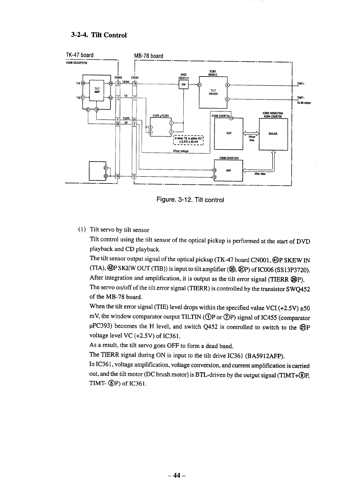
3-2-4. Tilt Control
TK-47board MB-78 board
IC006SSI33P3720
| | CNO06 TIERRcN452
T_
TIB_ TfE
jL..__ TIOFS
0452
2SD2114
Offsetvoffaoe
1(;361
BA5912
TILT t
DRIVER
OSP
tC806 CDXE730R
ARP
IC8051,10_7034
1C804_8
$H/LGA
t,litter
1
1
i
l TIMT÷
I TIMT-
To_ll_m
I
I
I
J
Figure. 3-12. Tilt control
(1) Tilt servo by tilt sensor
Tilt control using the tilt sensor of the optical pickup is performed at the start of DVD
playback and CD playback.
The tilt sensor output signal of the optical pickup (TK-47 board CN001, (_)P SKEW IN
(TIA), _P SKEW OUT (TIB)) is input to tilt amplifier (_), _)P) of IC006 (SS 13P3720).
After integration and amplification, it is output as the tilt error signal (TIERR _)P).
The servo on/off of the tilt error signal (TIERR) is controlled by the transistor SWQ452
of the MB-78 board.
When the tilt error signal (TIE) level drops within the specified value VCI (+2.5V) +50
mV, the window comparator output TILTIN ((_)P or (_)P) signal of IC455 (comparator
pPC393) becomes the H level, and switch Q452 is controlled to switch to the _[])P
voltage level VC (+2.5V) of IC361.
As a result, the tilt servo goes OFF to form a dead band.
The TIERR signal during ON is input to the tilt drive IC361 (BA5912AFP).
In IC361, voltage amplification, voltage conversion, and current amplification is carried
out, and the tilt motor (DC brush motor) is BTL-driven by the output signal (TIMT+(_)P,
TIMT- (_)P) of IC361.
- 44 -
(2) Tilt offset adjustment minimizing jitter
To optimize RF during DVD playback (excluding search), the jitter (JITTER:time:axis
fluctuation of the RF signal) is measured, offset is added to the tilt servo loop, and the
jitter is minimized.
As jitter is adjusted at shipment, normally this adjustment is not required during playback.
However if the jitter deviates with time, the adjustment value may not be optimum
, according to the disc. In such cases, the jitter is measured prior to playback, and if it is
deviated from the specified value, adjustments are started automatically.
i.
The jitter value is measured by IC806 (CXD1865R) and the measured data is sent to
the system controller IC805 (HD6437034) to determine the offset amount. The offset is
voltage-generated by the PWM output of IC506 (DSP), and input to SSI33P3720 (_P
as the offset voltage (TIOFS).
By performing the above three types of IC control, the jitter is adjusted to optimum.
- 45 -
3-3. Servo Operation at CD and Video CD Playing
3-3-1. Optical Pickup Control
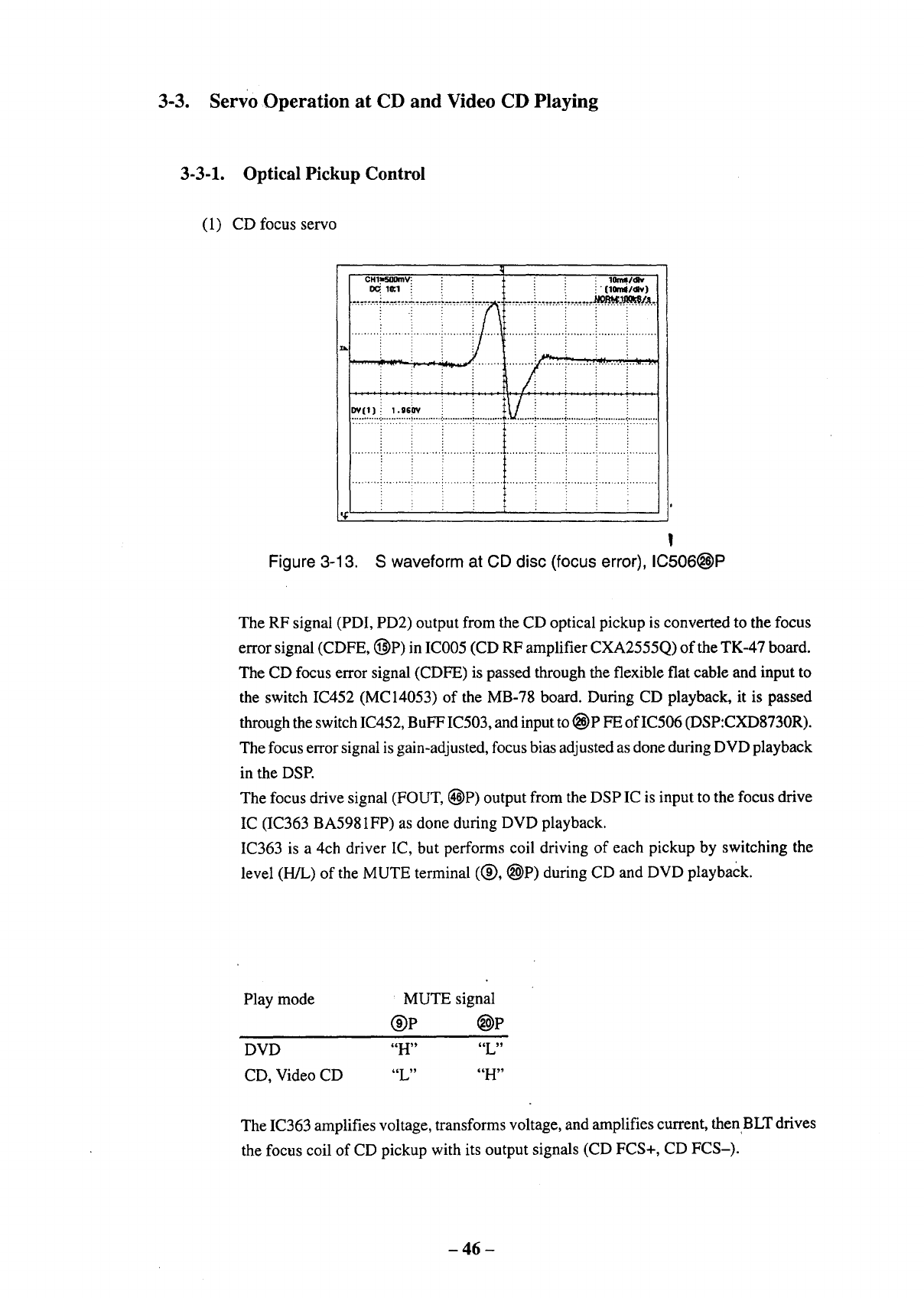
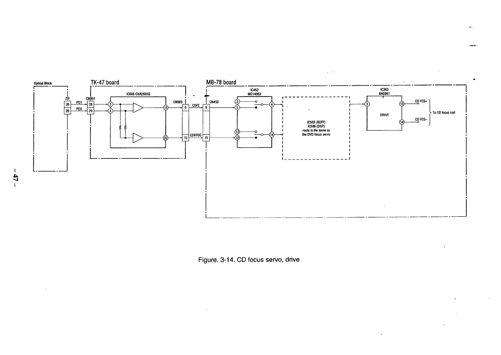
(1) CD focus servo
!
CH 1154]OmV: !lOtrnl/dlv
...................i.............................:.............................::.........i........
...................ii.............................t.............................!.........!.........
I
................... {............................. ! ............................. :......... _.........
1
:'i .... T ,, , • . •
!
Figure 3-13. S waveform at CD disc (focus error), IC506_)P
The RF signal (PDI, PD2) output from the CD optical pickup is converted to the focus
error signal (CDFE, (_)P) in IC005 (CD RF amplifier CXA2555Q) of the TK-47 board.
The CD focus error signal (CDFE) is passed through the flexible flat cable and input to
the switch IC452 (MC14053) of the MB-78 board. During CD playback, it is passed
through the switch IC452, BuFF IC503, and input to _)P FE of IC506 (DSP:CXD8730R).
The focus error signal is gain-adjusted, focus bias adjusted as done during DVD playback
in the DSP.
The focus drive signal (FOUT, _P) output from the DSP IC is input to the focus drive
IC (IC363 BA5981FP) as done during DVD playback.
IC363 is a 4ch driver IC, but performs coil driving of each pickup by switching the
level (H/L) of the MUTE terminal ((_), _P) during CD and DVD playback.
Play mode MUTE signal
_)P _P
DVD "H .... L"
CD, Video CD "L .... H"
The IC363 amplifies voltage, transforms voltage, and amplifies current, then BLT drives
the focus coil of CD pickup with its output signals (CD FCS+, CD FCS-).
- 46 -
I
I
OpticalBlock TK-47board
I
ZIF CNO01
IC005 CXA2555Q
CNO05
i
JI
|
L
|
MB-78 board
D
CN452
IC452
MC14053
I
I
I
I
I
I_
IC503(BUFF)
IC506 (DSP)
routeis the sameas
the DVDfocusservo
IC363
BA5981
DRIVE
C_ FCS* 1
To CD focuscoil
_cs-j
1
i
L_.
Figure. 3-14. CD focus servo, drive
(2) CD tracking servo
From
optical
block
TK-47 board
s
IC005
CXA25550
c[
MB-78 board
IC452 IC503
MC14053 NJM3403 IC506
CXD8730 le_3
BA5981
ToCO_up
trackingcoil
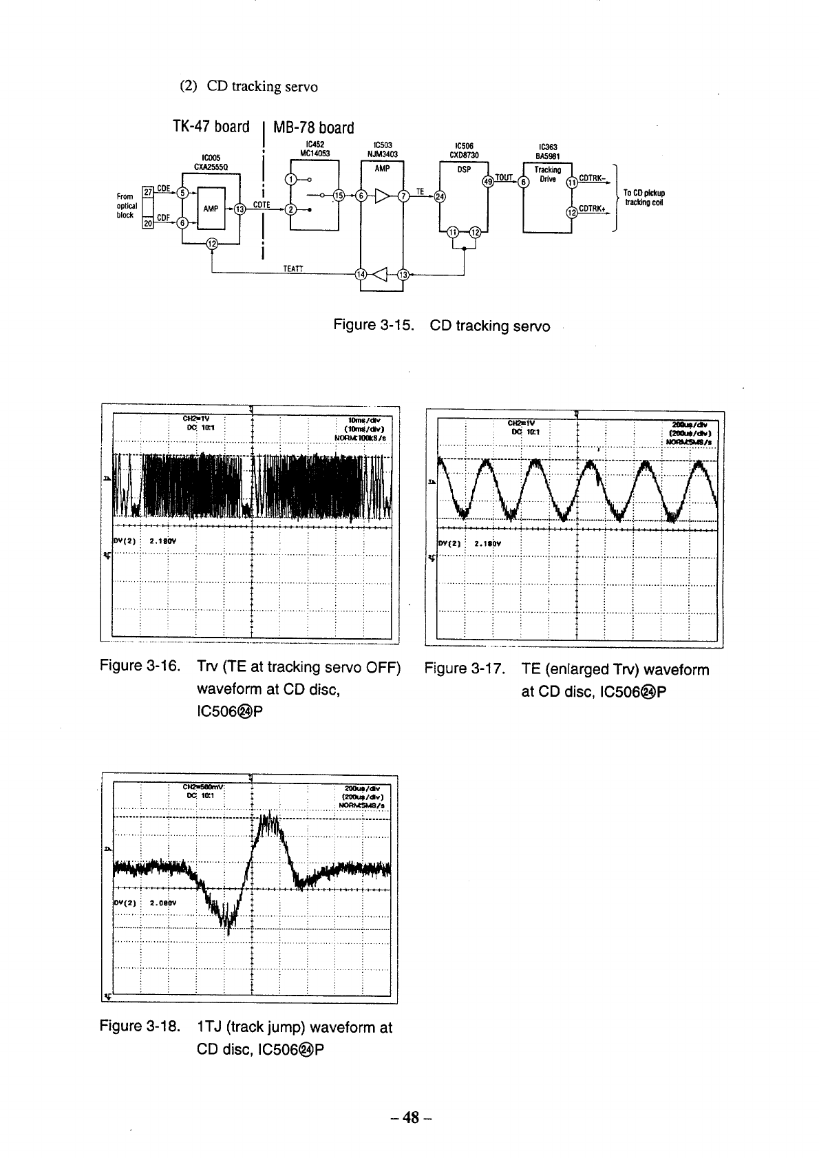
Figure 3-15. CD tracking servo
Figure 3-16. Try (TE at tracking servo OFF)
waveform at CD disc,
IC5061_)P
iCH2=lV i i 2muild_
.OC I_I - i (2Wu*/d_]
! :: i i _/,
................... i ......... i................... t ...... _! ......... ! ................... !.........
,.j
i+.
_(zl : z.1#_
'_i.........i.........i.....................................................................i.........
.........:........._..................._.........•.......................................;........
:?
Figure 3-17. TE (enlarged Try) waveform
at CD disc, IC506(_)P
cmn,,_mv: !Zoo_,/a_v
:iNO_M:SM_Is
........ ÷....... ÷....... _........ _....... _," _........ ._....... .;........ F........
o',',i'.o'_ i_,i/_ i i i i
................................................. ÷ ................................................
.............................i........._:........._.................................................
• . : , :: !
Figure 3-18. 1TJ (track jump) waveform at
CD disc, IC506(_)P
- 48 -
The CDE and CDF signals output from the CD optical pickup are converted to the CD
tracking error signal (CDTE (_)P) at IC005 of (CXA2555Q) the TK-47 board. -
The CDTE signal is input to the switch IC (IC452, MC1405'3) of the MB-78 board.
During CD playback, it is passed through the switch IC (IC452), amplified at IC503,
and input to _)P TE of IC506 (DSP CXD8730R).
Like DVD playback, the tracking error signal is gain-adjusted, tracking bias-adjusted,
and tracking auto level-adjusted in the DSP.
The DSP tracking drive signal (T OUT (_)P) is voltage-amplified, voltage-converted,
and .current-amplified by the IC (IC363 BA5981) for tracking driving, and used to
drive the CD pickup tracking coil.
Track jump control during CD search is carried out by IC506 (DSP CXD8730R) as
done during DVD search.
As a result, when performing 1 track jump or N track jump (many track jumps), tracking
pulses are generated, the tracking zero cross timing is detected, tracking brake is
controlled, and the number of track jumps is measured.
* Tracking auto level adjustment.
This function operates only during CD and V-CD playback.When the TE level (traverse
waveform) is small due to the inconsistency of the disc, this level adjustment is
performed to eliminate the inconsistencies. Consequently, like gain adjustment, the
adjustment is performed each time the disc is replaced (tray is opened), to set the
traverse level to 2.0 Vp-p.
After setting the disc and turning ON the focus servo, the peak-to-peak value of the TE
signal (this TE signal is called the traverse signal) is measured by the IC506
(DSP:CXD8730R).
The|measurement results are read by the IC805 (system control IC) to determine the
gain variable amount. The response (variable amount) is then returned again to IC506
f
(DSP:CXD8730R).
Upon receiving this, IC506 outputs control signal for the tracking auto level adjustment
from (_)P and (_P of the IC506 (DSP:CXD8730R). It is added by IC503 and converted
to the analog voltage (TEATT signal).
The TEATr signal is input to _)P of IC005 (CXA2555) of the
TK-47 board, and gain-controlled inside the IC. The variable width is about _+3.0 dB.
- 49 -
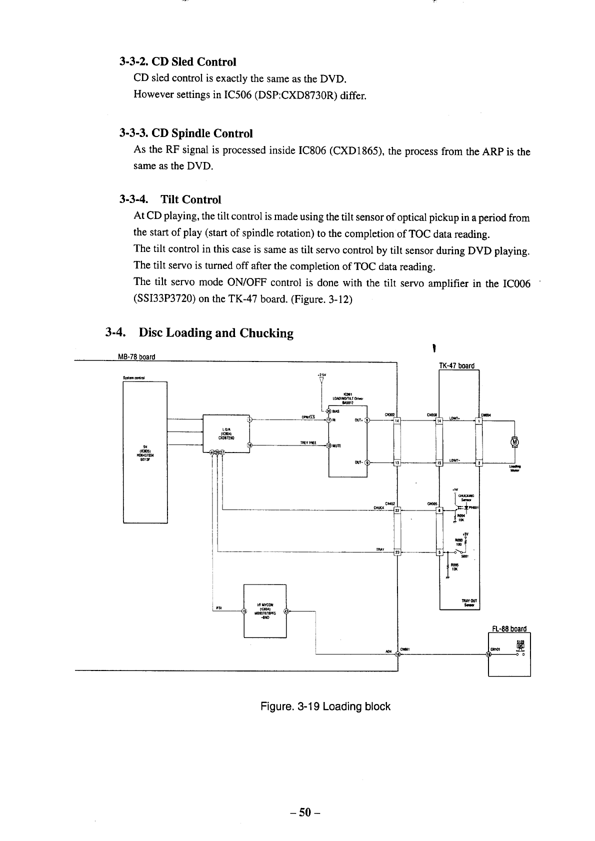
3-3-2. CD Sled Control
CD sled control is exactly the same as the DVD.
However settings in IC506 (DSP:CXD8730R) differ.
3-3-3. CD Spindle Control
As the RF signal is processed inside IC806 (CXD1865), the process from the ARP is the
same as the DVD.
3-3-4. Tilt Control
At CD playing, the tilt control is made using the tilt sensor of optical pickup in a period from
the start of play (start of spindle rotation) to the completion of TOC data reading.
The tilt control in this case is same as tilt servo control by tilt sensor during DVD playing.
The tilt servo is turned off after the completion of TOC data reading.
The tilt servo mode ON/OFF control is done with the tilt servo amplifier in the IC006
(SSI33P3720) on the TK-47 board. (Figure. 3-12)
3-4. Disc Loading and Chucking
MB-78board
HO_3r_
S013_
IIC_)
C_t_2eO
LOADff_w_TU.TOfkqz
T_Y _t
C_
CKUCK CN00S
)C_01
!
TK-47board
C_l, !LOM1. •
, LOUT- •
I (_lCXlt_
n
,,w
t_
FL-88board
Figure. 3-19 Loading block
- 50 -
Disc loading, unloading, and chucking operations are performed with one DC motor. Its
block diagram is dhown in Figure 3-19.
3-4-1. Motor Driver
The system controller IC (IC805) controls the open and close of the tray. It monitors the
sensors of the mechanism and
conti:ols the operations of the tray motor via the L G/A IC (IC804).
The tray open/close signal is output by 3-state PWM modulation from IC804.
H (5V) = Open
High Z = Stop
L (Gnd)= Close
The tray speed is controlled by increasing/decreasing the PWM duty ratio.
The TRAY FREE signal is used to control the Mute terminal of the driver directly, turn OFF
the motor drive, and free the operations.
During the stop state, the potential difference between the two terminals of the motor is
controlled to 0V, while during the Tray Free state, the motor is not controlled at all.
3-4-2. Tray Position Detection
Tray position detection is carded out by the chucking sensor PH001 and tray out sensor
S001 on the TK-47 board. These signals are input to the MB-78 board via the flexible flat
cable, and input to L G/A (IC804) CHUCK _)P, and TRAY _P.
The relation between tray position and sensor signals is as shown below:
Mode <TRAY OUT (CN005(_))> <CHUCKING (CN005(_))>
Tray out position H L
Tray opefating L L
Chucking position L H
!
-51 -
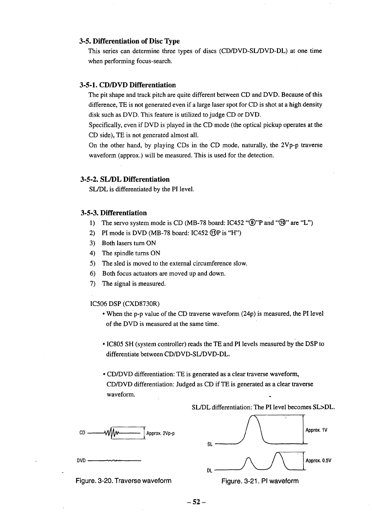
3-5. Differentiation of Disc Type
This series can determine three types of discs (CD/DVD-SL/DVD-DL) at one time
when performing focus-search.
3-5-1. CD/DVD Differentiation
The pit shape and track pitch are quite different between CD and DVD. Because of this
difference, TE is not generated even if a large laser spot for CD is shot at a high density
disk such as DVD. This feature is utilized to judge CD or DVD.
Specifically, even if DVD is played in the CD mode (the optical pickup operates at the
CD side), TE is not generated almost all.
On the other hand, by playing CDs in the CD mode, naturally, the 2Vp-p traverse
waveform (approx.) will be measured. This is used for the detection.
3-5-2. SL/DL Differentiation
SL/DL is differentiated by the PI level.
3-5 -3.
1)
2)
3)
4)
5)
6)
7)
Differentiation
The servo system mode is CD (MB-78 board: IC452 "(_)"P and "(_" are "L")
PI mode is DVD (MB-78 board: IC452 (_)P is "H")
Both lasers turn ON
The spindle turns ON
The sled is moved to the external circumference slow.
Both focus actuators are moved up and down.
The signal is measured.
IC506 DSP (CXD8730R)
•When the p-p value of the CD traverse waveform (24p) is measured, the PI level
of the DVD is measured at the same time.
• IC805 SH (system controller) reads the TE and PI levels measured bythe DSP to
differentiate between CD/DVD-SL/DVD-DL.
• CD/DVD differentiation: TE is generated as a clear traverse waveform,
CD/DVD differentiation: Judged as CD if TE is generated as a clear traverse
waveform.
CD __h_ I Approx. 2Vp-p
SL/DL differentiation: The PI level becomes SL>DL.
•_'IApprox.1V
SL
OVO ----.... -
Figure. 3-20. Traverse waveform
DL
Figure. 3-21. PI waveform
,rox.0.5V
-52 -
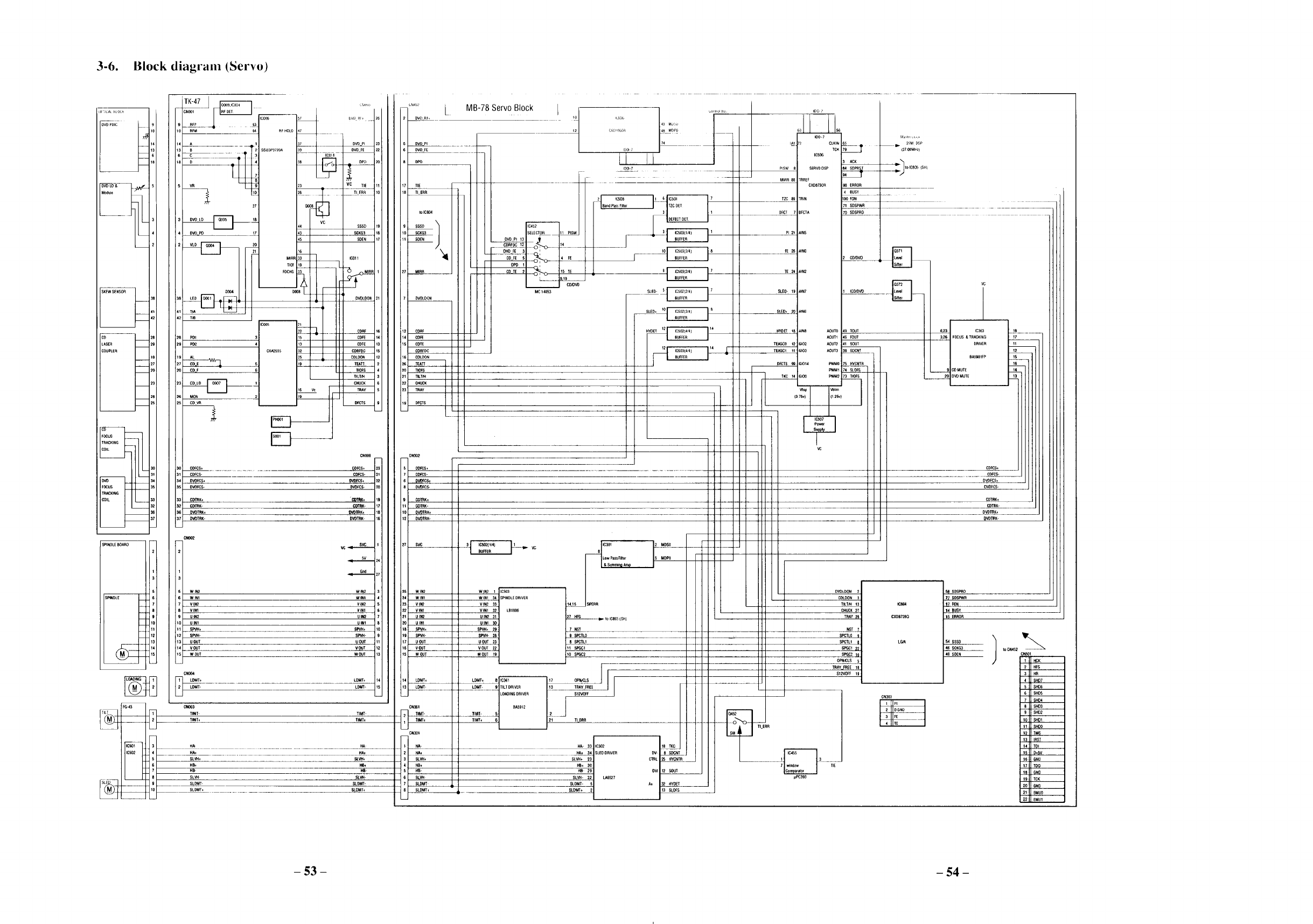
3-6. Block diagram (Servo)
,_ :k;AL _LOCK
DVDPDIC 9
14
18
S
38
4t
42
t9
27
20
23
26
25
FOCUS
TRACKING
COIL
3O
TR._KtNG
COIL i
SPINDLEBOARO
JTK-47 J
9_ icoo6 57
lO RFU 64 _F HOLO4Z
14 A ........ 1 37
13 B 2 ssi33P372oA 39
R C .... 3
_e D 4 38
7
5 VR 23
26
27 _08
3OVULO _VC
41
4 OVDPO lr 43
MIRa
TIOF
FOCHG
29 PD2 4
CX_SS5
19 AL
27 E
2O CD.F F
23 cp LC i
_ cx/_2555 _ I I- ---- 16 VC
121
uv_) Rh
DVDP_
OVDFE
_Pa
VC Tie
•TIERR
ssso
COKG3
i(:Oll
CRRF
COTE
CORFOC
COLCON
tEAl1
t_OFS
CHUCK
TRAY
_CTS
C_(
COFCR+
D_,FCS-
c¢_x,
CDTRK-
C_008
DVDTRK,
OYOTRK-
WIN2
WlNt
VlN2
VINt
CIN2
UIN1
SPVH,
SPVH-
UCOT
VCOT
w OUT
131
151 WIN2
]RL WiN1
17L VIN2
I81 Wm
I 9 I UIN2
]tOL UIN1
J'L s_.
It2L RPVH.
bUL uout
114L vOut
bSL wOUT
CNOO4
LDMT÷
LDMT-
LDMT+
LDMT-
1-43 CN0O3
TIMT.
TIMT,
TIMT-
TIMT*
IC501 HA
IC502 HA_ .............
Ti_7-
HB*
HB-
__ SLVH
SLDMT-
HA
SLVH+
He,
HB-
SLVH-
SLOMT-
SLOMT+
DVO FE
OPD
C_3OZ
I_I OFCS+
_U-
OVDFCS-
COr_K+
COTRK- '
RVDTRK÷
RVDTRK-
S_
w IN2
W I_1
VIN2
ViN1
U IN2
U IR1
S_VH÷
SPVH-
U OUT --
VOUT
WOUT
LDMT*
ON3_I
[_ TIMT_
TIMT_
CNU0_
SL_
_DMT
SLDMT*
L MR-78 Servo Block t
TI_ERR
OVOLDON
CRLDON
TILT/H
NUT
SPCTLI
SPGCl
OPNtCLS
S12VOFF
_1op
(375v)
CXDB728Q
2zM DSP
<27OOMHz)
<s.i
FON
IC363
DRWER
8A5981FP
CR/OVO
MC14053
W,IN2 1 IC303
WIN1 34 SPINDLEDRiVER
VIN2 33
VINI 32 LB1896
UIN2 31
UIN1 _0
U_H._ _NST
SPVH- 28 9 SPCTLO
UOUT 23 sS_CTL1
VOUT 22 seGcl
WOUT 19 SFGC2
LDMT- 9 TILTDRIVER 13 TRAYFREE
LOADINGDRIVER S12VOFF
BASg_2
TIMT- 5 2
TIM% 6 TI=E_R
ITS06
MUt,O
CXDI86!,R MDpo
ID_
HA- 311C302
HA* 34 SLEDORIVER
SLVH+ 23
_30
Ha 29
SLVH- Lk6527
SLDMT- A*
ULDMT+
IA1.
PISW
TZ¢
DFCT
FE
te
$LEO-
SLED*
HYRET
TEACCO
TEAGCI
OETS
CN303
IPI
DGND
CDFCS-
RVO_CS*
OVDFCS-
CDTRK+
CO_K-
DVDmK_
D_TRK-
SSSD 1
SCKG3 toCN4S2 _
SDEN CN501
1 kICK
2 NFS
3HR
4 UHD7
5 SHD6
6 SHD5
7SHD4
SSHD3
g SHD2
F0 SHD!
ll SHDU
t2 TMS
13 IRST
14 TOI
lS D*_V
16 GNU
17 TOO
I_ GNp
19 TCK
2O GND
2_ EMU0
22 _MUl
- 53 - - 54 -
4. IC PIN DESCRIPTION
4-1. ARP
CXD1865R (IC806 oil MB-78 board)
4-1-1. Block Diagram
13T-139, 141-143,
145-147, 149:MAO-MA9
113:WFCK 150:XMWR
114:SC0R 151:XCAS
116:EXCK 153:XRAS
50:DEC1 117:SBSO 154:XOE
51:NORF 119:SOS0 156-159, 161-164,
52:JITPWM 55:FWON 120:SOCK 166-169, 171-174:MDOO-MD15
T Out,,ut"--
.... ,protec,.on.'' ontro'I %
]_ NpM__[ Ope- I __ Built-in _ ECC-core I. _
27.y__a plifierl CLVcontrol memory L-II_.I signal /
" _ _gLesiegrnatI,°n_ _ Iprocessing[_'--"
IO:RI:-IN1
12:RFIN2
lg:AOUT_
124:SCKI
2:PLCKO_
35:VCOIN c,oc
control CPU I/F
43:MDSO 56:XWR
46:MDS1 57:XRD
48:MDPO 59-62, 64-67:DO-D7
49:MDP1 70-73, 75-78:AO-A7
47:MON 80:XlNT
53:LOCK 81:XCS
83:XWAT
84:XRST
90:SDCK
91:XSHD
92:XSRO
93:XSAK
94:SDEF
96-99, 101-104:SDO-SDt
106:DATA
107:BCLK
108:LRCK
109:DOUT
110:MUTE
112:MD2
55 - - 56 -
4-1-2. Pin Functions
Pin No.
1
2
3
4
5
6
7
8
9
10
11
12
13
14
15
16
17
18
19
20
21
22
23
24
25
26
27
28
29
30
31
32
33
34
35
36
37
38
39
40
Signal Name
PLCKI
PLCKO
VSS
i RFD
VDD
v_s1
VRB
VRBS
GNDA1
RFIN1
AIN
RFIN2
VCCA1
VRTS"
VRT
VDD1
VSS2
VDD2
AOUT
VCCA2
IREF
VREF
COMP
I_IAS
GNDA2
VCCA3
Y
FR1
FR2
FR3
INM
INP
GNDA3
GNDA4
VCOIN
R1
R2
TEST0
VCCA4
VCK
Direction
I
O
P
B
P
ADP
AI
AI
AP
AI
AI
AI
AP
AI
AI
ADP
ADP
ADP
AO
AP
AI
AI
AI
AI
AP
AP
AO
AO
AO
AO
AI
AI
AP
AP
AI
AI
AI
AO
AP
B
Level
3.3
3.3
3.3
3.3
5
5
3.3
3.3
3.3
3.3
Function
PLCK input
PLCK output
Digital ground
RF2 value data input/output
Digital positive power supply
Digital ground
ADC reference
ADC reference
Analog ground
RF input
RF input
RF input
Analog positive power supply
ADC reference
ADC reference
Digital positive power supply
Digital ground
Digital positive power supply
DAC output
Analog positive power supply
DAC reference current
DAC reference voltage
DAC compensation pin
DAC bias pin
Analog ground
Analog positive power supply
Ope-amplifier output
Feedback resistance switching 1
Feedback resistance switching 2
Feedback resistance switching 3
Ope-amplifier negative input
Ope-amplifier positive input
Analog ground
Analog ground
VCC control input
VCO external resistor 1
VCO external resistor 2
VCO test output
Analog positive power supply
VCO oscillation output/test input
-57 -
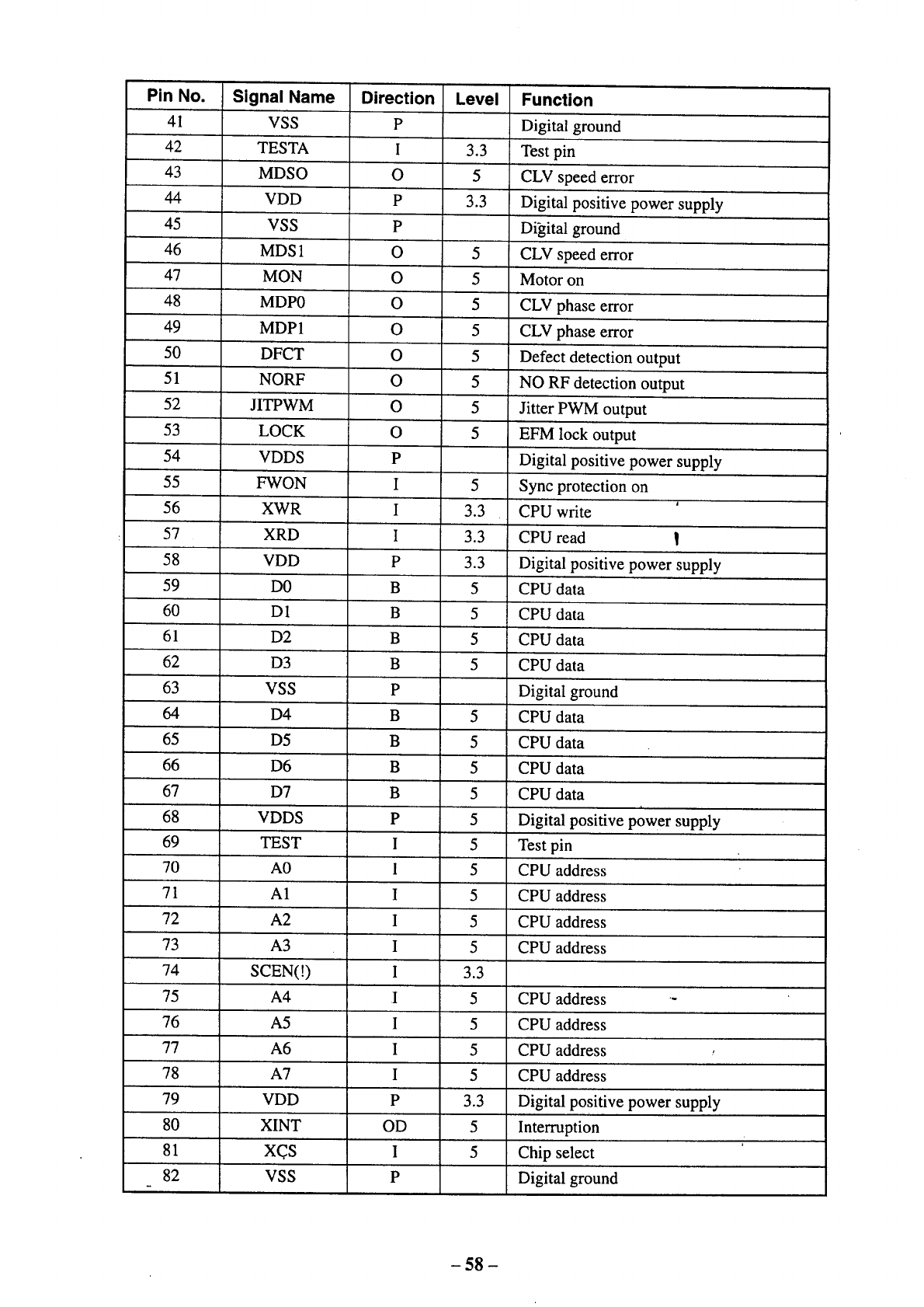
Pin No.
41
42
43
44
45
46
47
48
49
50
51
Signal Name
VSS
TESTA
MDSO
VDD
VSS
MDS 1
MON
MDP0
MDP1
DFCT
NORF
Direction
P
I
0
P
P
0
0
0
0
0
0
Level
3.3
5
3.3
5
5
5
5
5
5
Function
Digital ground
Test pin
CLV speed error
Digital positive power supply
Digital ground
CLV speed error
Motor on
CLV phase error
CLV phase error
Defect detection output
NO RF detection output
52
53
54
55
56
57
58
59
60
61
62
63
64
65
66
67
68
69
70
71
72
73
74
75
76
77
78
79
80
81
82
JITPWM
LOCK
VDDS
FWON
XWR
XRD
VDD
DO
D1
D2
D3
VSS
D4
D5
D6
D7
VDDS
TEST
A0
A1
A2
A3
SCEN(!)
A4
A5
A6
A7
VDD
XINT
XCS
VSS
O
O
P
I
I
I
P
B
B
B
B
P
B
B
B
B
P
I
1
I
I
I
I
I
I
I
I
P
OD
I
P
5
5
5
3.3
3.3
3.3
5
5
5
5
5
5
5
5
5
5
5
5
5
5
3,3
5
5
5
5
3.3
5
5
Jitter PWM output
EFM lock output
Digital positive power supply
Sync protection on
CPU write
CPU read l
Digital positive power supply
CPU data
CPU data
CPU data
CPU data
Digital ground
CPU data
CPU data
CPU data
CPU data
Digital positive power supply
Test pin
CPU address
CPU address
CPU address
CPU address
CPU address
CPU address
CPU address
CPU address
Digital positive power supply
Interruption
Chip select
Digital ground
-58-
Pin No.
83
84
85
86
87
88
89
90
91
92
93
94
95
96
97
98
99
100
101
102
103
104
105
106
107
108
109
110
111
112
113
114
115
116
117
118
119
120
121
122
123
124
Signal Name
XWAT
XRST
VDD
TEST0
SCMD
" ETST
VSS
SDCK
XSHD
XSRQ
XSAK
SDEF
VDD
SDO
SD1
SD2
SD3
VSS
SD4
SD5
SD6
SD7
VDD
DATA
BCLK
URCK
I_OUT
MUTE
VSS
MD2
WFCK
SCOR
VDDS
EXCK
SBSO
VSS
SQSO
SQCK
VSS
MCKI
VDDS
SCKI
Direction
OD
I
P
I
I
I
0
0
I
0
0
P
o (B)
O (B)
O (B)
o (a)
P
o (a)
o (B)
0 (B)
O (B)
P
O
O
O
O
I
P
I
O
O
P
I
O
P
O
I
P
I
P
I
Level
5
5
3.3
3.3
3.3
3.3
3.3
3.3
3.3
3.3
3.3
3.3
3.3
3.3
3.3
3.3
3.3
3.3
3.3
3.3
3.3
3.3
3.3
3.3
3.3
5
5
5
5
5
5
5
5
5
5
5
5
Function
Wait
Reset
Digital positive power supply
Test pin
Test pin
Test pin
Digital ground
SD bus clock
SD bus header
SD bus REQ
SD bus ACK
SD bus error flag
Digital positive power supply
SD bus data
SD bus data
SD bus data
SD bus data
Digital ground
SD bus data
SD bus data
SD bus data
SD bus data
Digital positive power supply
CDDA data
CDDA bit clock
CDDA LR clock
Digital out
Audio mute
Digital ground
Digital out on
Frame clock
Subcode sync
Digital positive power supply
SBSO reading clock
SubP to W serial output
Digital ground
SubQ serial output
SBSO reading clock
Digital ground
ECC clock
Digital positive power supply
System clock
-59 -
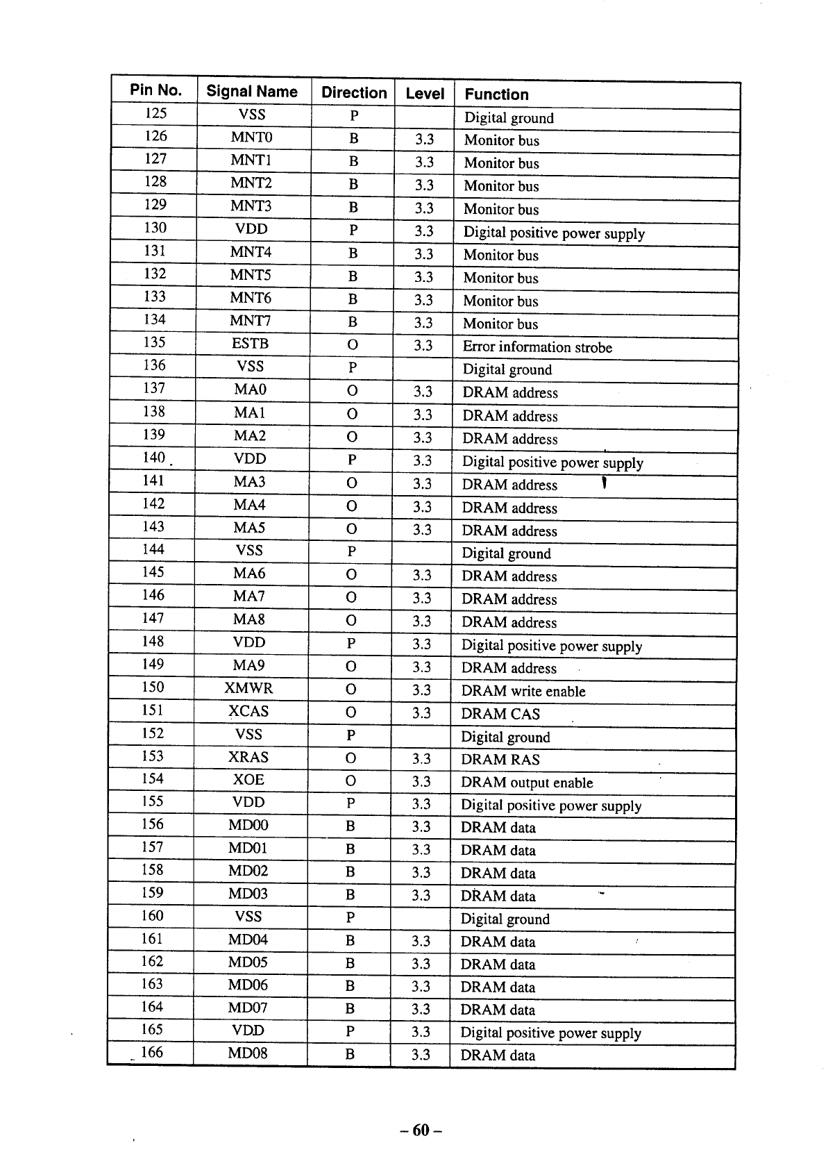
Pin No.
125
126
127
128
129
130
131
132
133
134
135
136
137
138
139
140
141
142
143
144
145
146
147
148
149
150
151
152
153
154
155
156
157
158
159
160
161
162
163
164
165
166
Signal Name
VSS
MNT0
MNT1
MNT2
MNT3
VDD
MNT4
MNT5
MNT6
MNT7
ESTB
VSS
MA0
MA1
MA2
VDD
MA3
MA4
MA5
VSS
MA6
MA7
MA8
VDD
MA9
XMWR
XCAS
VSS
XRAS
xoz
VDD
MD00
MD01
MD02
MD03
VSS
MD04
MD05
MD06
MD07
VDD
MD08
Direction
P
B
B
B
B
P
B
B
B
B
O
P
O
O
O
P
O
O
O
P
O
O
O
P
O
O
O
P
O
O
P
B
B
B
B
P
B
B
B
B
P
B
Level
3.3
3.3
3.3
3.3
3.3
3.3
3.3
3.3
3.3
3.3
3.3
3.3
3.3
3.3
3.3
3.3
3.3
3.3
3.3
3.3
3.3
3.3
3.3
3.3
3.3
3.3
3.3
3.3
3.3
3.3
3.3
3.3
3.3
3.3
3.3
3.3
3.3
Function
Digital ground
Monitor bus
Monitor bus
Monitor bus
Monitor bus
Digital positive power supply
Monitor bus
Monitor bus
Monitor bus
Monitor bus
Error information strobe
Digital ground
DRAM address
DRAM address
DRAM address
!
Digital positive power supply
DRAM address !
DRAM address
DRAM address
Digital ground
DRAM address
DRAM address
DRAM address
Digital positive power supply
DRAM address
DRAM write enable
DRAM CAS
Digital ground
DRAM RAS
DRAM output enable
Digital positive power supply
DRAM data
DRAM data
DRAM data
DRAM data "
Digital ground
DRAM data
DRAM data
DRAM data
DRAM data
Digital positive power supply
DRAM data
- 60 -
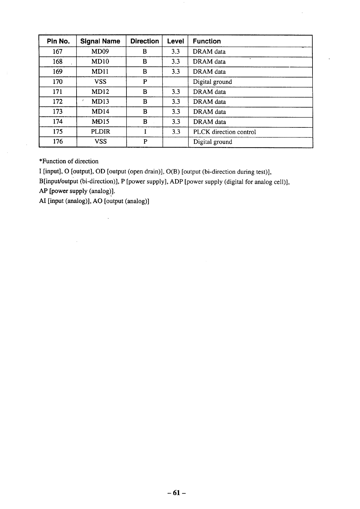
Pin No.
167
i68
169
170
171
172
173
174
175
176
Signal Name
MD09
MD10
MDll
VSS
MD12
MD13
MD14
M-D15
PLDIR
VSS
Direction
B
B
B
P
B
B
B
B
I
P
Level
3.3
3.3
3.3
3.3
3.3
3.3
3.3
3.3
Function
DRAM data
DRAM data
DRAM data
Digital ground
DRAM data
DRAM data
DRAM data
DRAM data
PLCK direction control
Digital ground
*Function of direction
I [input], O [output], OD [output (open drain)], O(B) [output (bi-direction during test)],
B[input/output (bi-direction)], P [power supply], ADP [power supply (digital for analog cell)],
AP [power supply (analog)].
AI [input (analog)], AO [output (analog)]
- 61 -
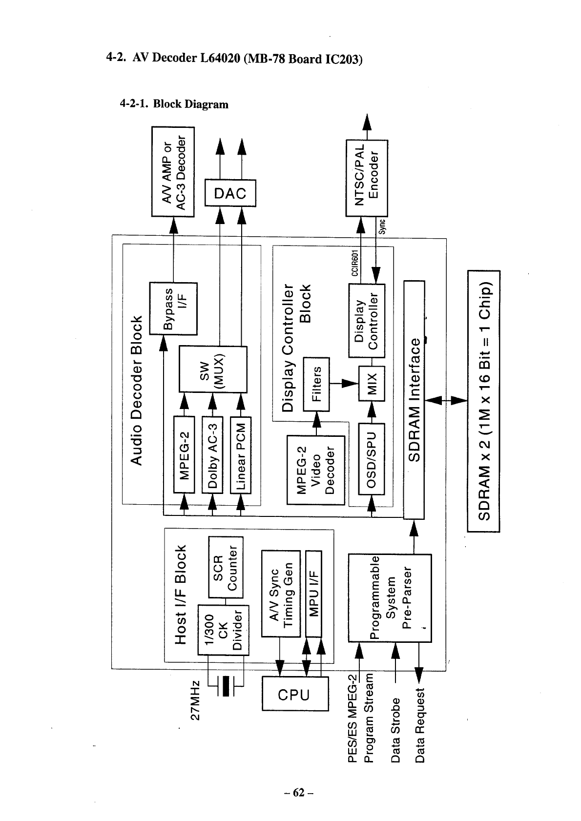
4-2. AV Decoder L64020 (MB-78 Board IC203)
4-2-1. Block Diagram
c-
O
II
rn
x
v
o,1
x
<
a
co
- 62 -
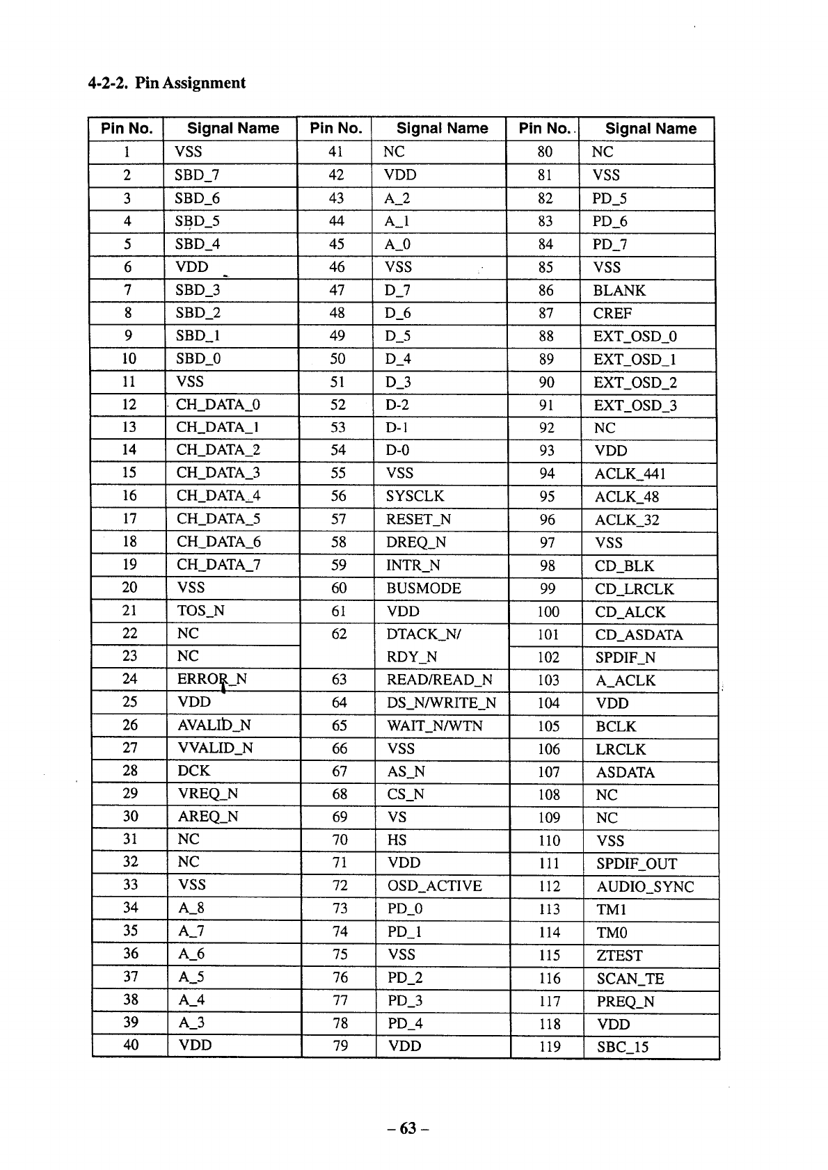
4-2-2.Pin Assignment
Pin No.
1
2
3
4
5
6
7
8
9
10
11
12
13
14
15
16
17
18
19
20
21
22
23
24
25
26
27
28
29
30
31
32
33
34
35
36
37
38
39
40
Signal Name
VSS
SBD_7
SBD_6
SBD_5
SBD_4
VDD
SBD_3
SBD_2
SBD1
SBD_0
VSS
CH_DATA_0
CH_DATA_I
CH_DATA_2
CH_DATA_3
CH_DATA,_4
CH_DATA_5
CH_DATA_6
CH_DATA_7
VSS
TOS_N
NC
NC
ERRO__N
VDD
AVALI__N
VVALID_N
DCK
VREQ_N
AREQ_N
NC
NC
VSS
A8
A7
A_6
A_5
A_4
A_3
VDD
Pin No.
41
42
43
44
45
46
47
48
49
5O
51
52
53
54
55
56
57
58
59
60
61
62
63
64
65
66
67
68
69
70
71
72
73
74
75
76
77
78
79
Signal Name
NC
VDD
A_2
A_I
A_0
VSS .-
D_7
D_6
D_5
D_4
D_3
D-2
D-l
D-0
VSS
SYSCLK
RESET_N
DREQ_N
INTR_N
BUSMODE
VDD
DTACK_N/
RDY_N
READ/READ_N
DS_N/WRITE_N
WAIT_N/WTN
VSS
AS_N
CS_N
VS
HS
VDD
OSD_ACTIVE
PD_0
PD_I
VSS
PD_2
PD_3
PD_4
VDD
Pin No..
80
81
82
83
84
85
86
87
88
89
90
91
92
93
94
95
96
97
98
99
100
101
102
103
104
105
106
107
108
109
110
111
112
113
114
115
116
117
118
119
Signal Name
NC
VSS
PD_5
PD_6
PD_7
VSS
BLANK
CREF
EXT_OSD_0
EXT_OSD_I
EXT_OSD_2
EXT_OSD_3
NC
VDD
ACLK_441
ACLK_48
ACLK_32
VSS
CD_BLK
CD_LRCLK
CD_ALCK
CD_ASDATA
SPDIF_N
A_ACLK
VDD
BCLK
LRCLK
ASDATA
NC
NC
VSS
SPDIF_OUT
AUDIO SYNC
TM1
TM0
ZTEST
SCAN_TE
PREQ_N
VDD
SBC_15
- 63 -
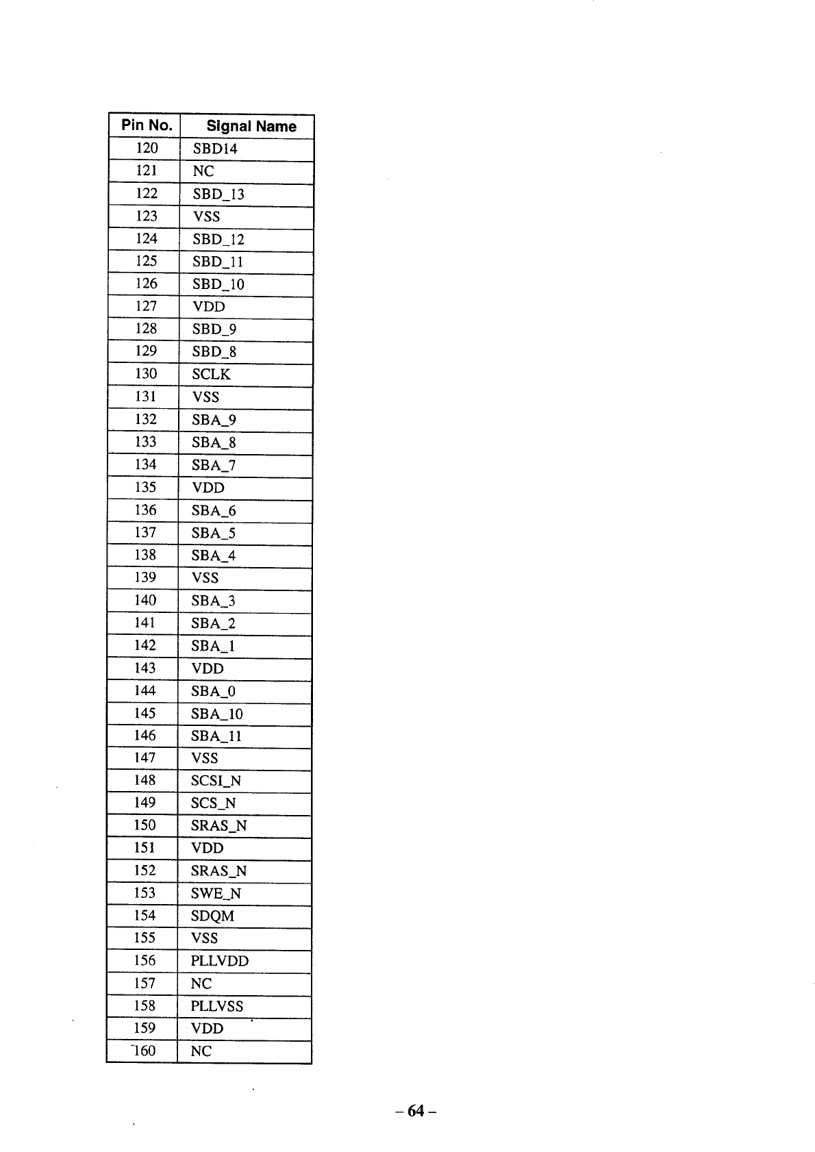
Pin No.
120
121
122
123
124
125
126
127
128
129
130
131
132
133
134
135
136
137
138
139
140
141
142
143
144
145
146
147
148
149
150
151
152
153
154
155
156
157
158
159
160
Signal Name
SBD14
NC
SBD_13
VSS
SBD_12
SBD_11
SBD_10
VDD
SBD_9
SBD_8
SCLK
VSS
SBA_9
SBA_8
SBA_7
VDD
SBA_6
SBA_5
SBA_4
VSS
SBA_3
SBA_2
SBA_I
VDD
SBA_0
SBA_10
SBA_ll
VSS
SCSI_N
SCS_N
SRAS_N
VDD
SRAS_N
SWEN
SDQM
VSS
PLLVDD
NC
PLLVSS
VDD
NC
- 64 -
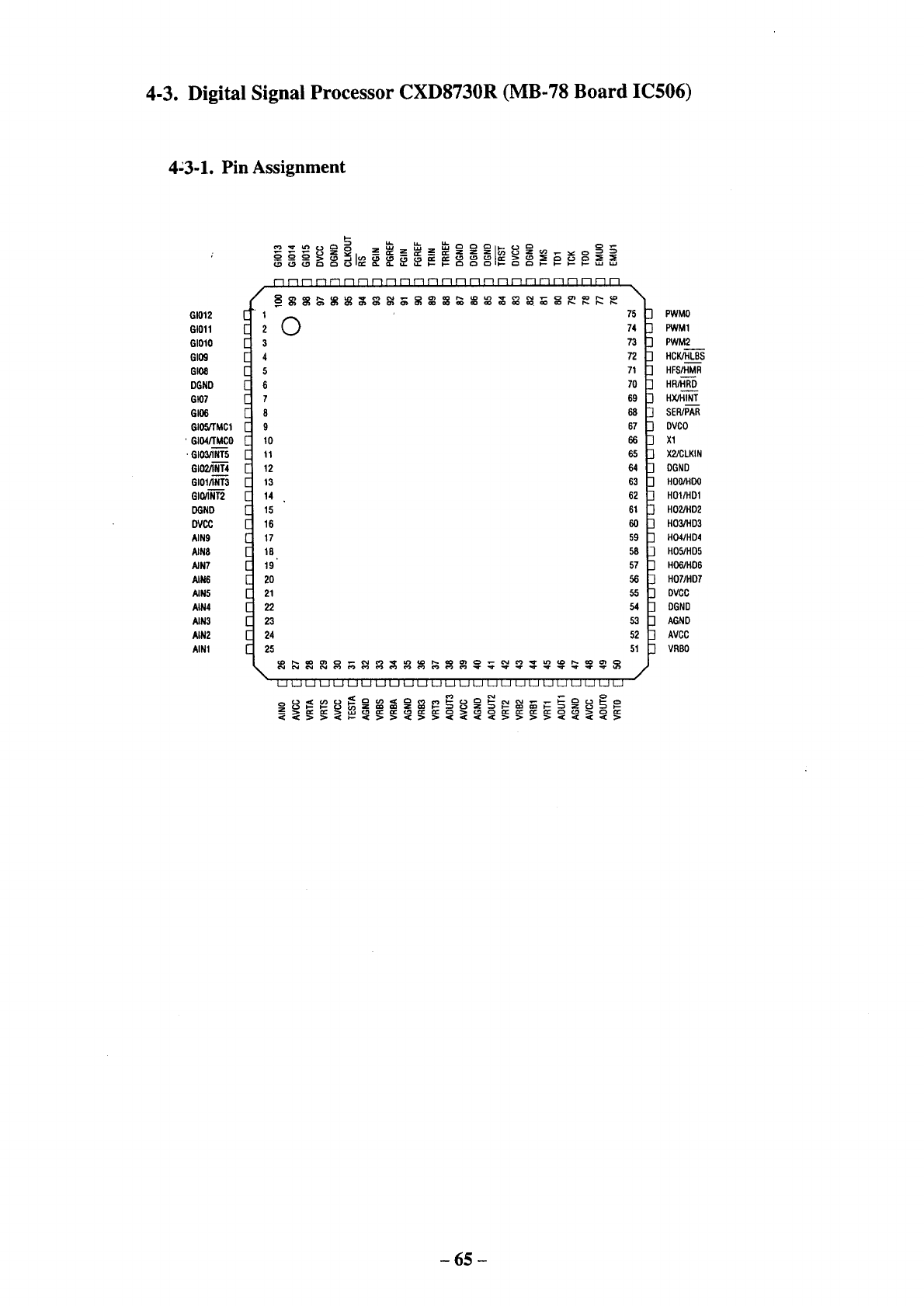
4-3. Digital Signal Processor CXD8730R (MB-78 Board IC506)
4:3-1. Pin Assignment
G1012
G1011
GI010
GI09
GI08
DGND
G}07
GI06
GIOS/TMC1
' GIO4/TMCO
' GlO3,qNT5
GIO2/INT4
GIO1ANT3
GI_INT2
DGND
DVCC
AIN9
AIN8
AIN7
AIN6
NN5
A|N4
AIN3
AIN2
AIN1
1 7 ]
2 (_ 74]
3 73 "l
4 72 -I
s 71 -1
670 "1
769 -1
I- 8 68 ]
[" 9 67 '-]
F lo 663
I- 11 65 -L
I- 12 64 -1
E13 63 3
I- 14 62 -1
[15 61
E 16 6o
[- 17 59
E _ 5_
[ _9 57
I- 20 56
[- 21 55
E22 54
I- 23 53
E24 52
[" 25 51
L_IL.._L_IL_IL_If._IL_Ii_IIIL_/L_.IL__L._L._JL_JL_IL_JL_JL_JL_J__ /
PWMO
PWM1
PWM2
HCWHLBS
HFS/HMR
HR/HRD
HX/HINT
SER/PAR
DVCO
Xl
X2/CLKIN
DGND
HOO/HDO
HOI/HD1
HO2/HD2
HO3/HD3
HO41HD4
HOS/'HD5
HO6/HD6
HO7IHD7
DVCC
DGND
AGND
AVCC
VRBO
- 65 -
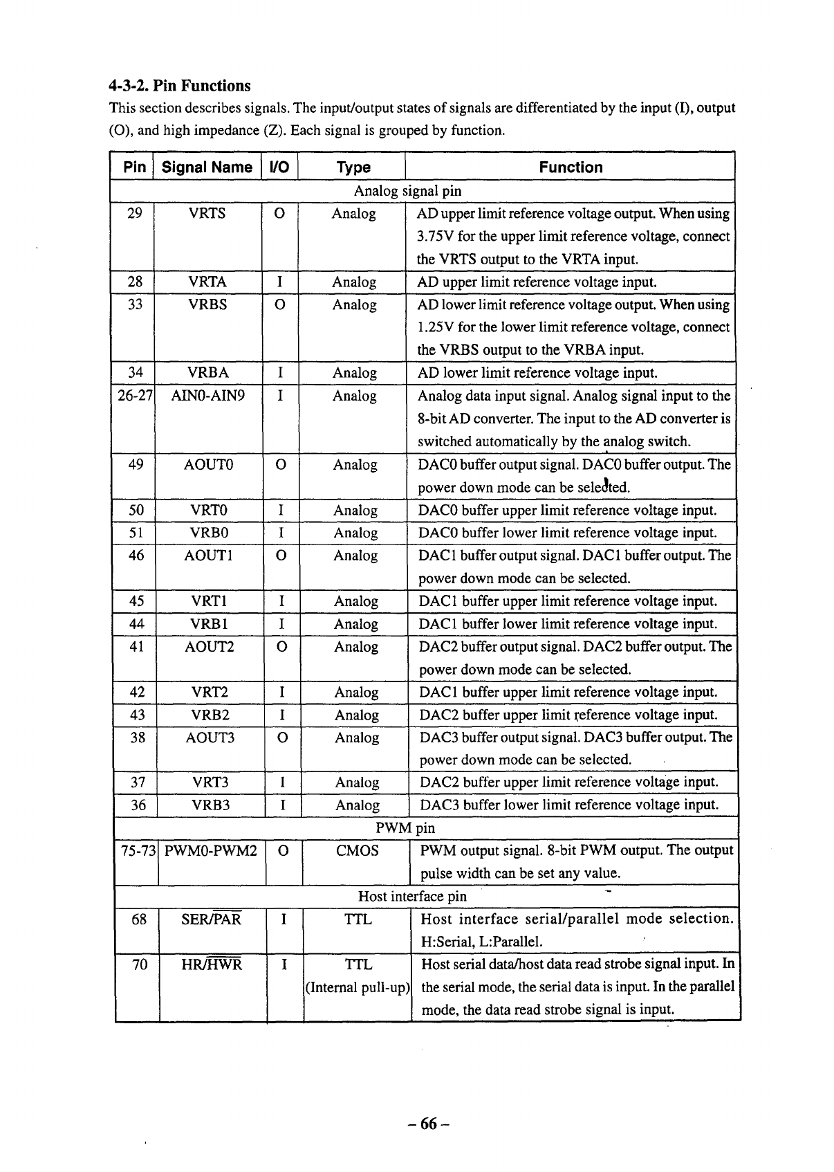
4-3-2. Pin Functions
This section describes signals. The input/output states of signals are differentiated by the input (I), output
(O), and high impedance (Z). Each signal is grouped by function.
Pin ]Signal Name I,I/0 I
29 VRTS O
28 VRTA I
33 VRBS O
34 VRBA I
26-27 AIN0-AIN9 I
49 AOUT0 O
50 VRT0 I
51 VRB0 I
46 AOUT1 O
45 VRT1 I
44 VRB 1 I
41 AOUT2 O
42 VRT2 I
43 VRB2 I
38 AOUT3 O
37 VRT3 1
36 VRB3 I
75-73 PWM0-PWM2 O
SER/PAR I
HR/HWR I
68
70
Type Function
Analog signal pin
Analog AD upper limit reference voltage output. When Using
3.75V for the upper limit reference voltage, connect
the VRTS output to the VRTA input.
Analog AD upper limit reference voltage input.
Analog AD lower limit reference voltage output. When using
1.25V for the lower limit reference voltage, connect
the VRBS output to the VRBA input.
Analog AD lower limit reference voltage input.
Analog Analog data input signal. Analog signal input to the
8-bit AD converter. The input to the AD converter is
switched automatically by the analog switch.
Analog DAC0 buffer output signal. DAC0 buffer output. The
power down mode can be seleJted.
Analog DAC0 buffer upper limit reference voltage input.
Analog DAC0 buffer lower limit reference voltage input.
Analog DAC 1 buffer output signal. DAC 1 buffer output. The
power down mode can be selected.
Analog DAC 1 buffer upper limit reference voltage input.
Analog DAC 1 buffer lower limit reference voltage input.
Analog DAC2 buffer output signal. DAC2 buffer output. The
power down mode can be selected.
Analog DAC 1 buffer upper limit reference voltage input.
Analog DAC2 buffer upper limit reference voltage input.
Analog DAC3 buffer output signal. DAC3 buffer output. The
power down mode can be selected.
Analog DAC2 buffer upper limit reference voltage input.
Analog DAC3 buffer lower limit reference voltage input.
PWM pin
CMOS PWM output signal. 8-bit PWM output. The output
pulse width can be set any value.
Host interface pin
TTL Host interface serial/parallel mode selection.
H:Serial, L:Parallel.
Host serial data/host data read strobe signal input. In
the serial mode, the serial data is input. In the parallel
mode, the data read strobe signal is input.
TrL
(Internal pull-up)
- 66 -
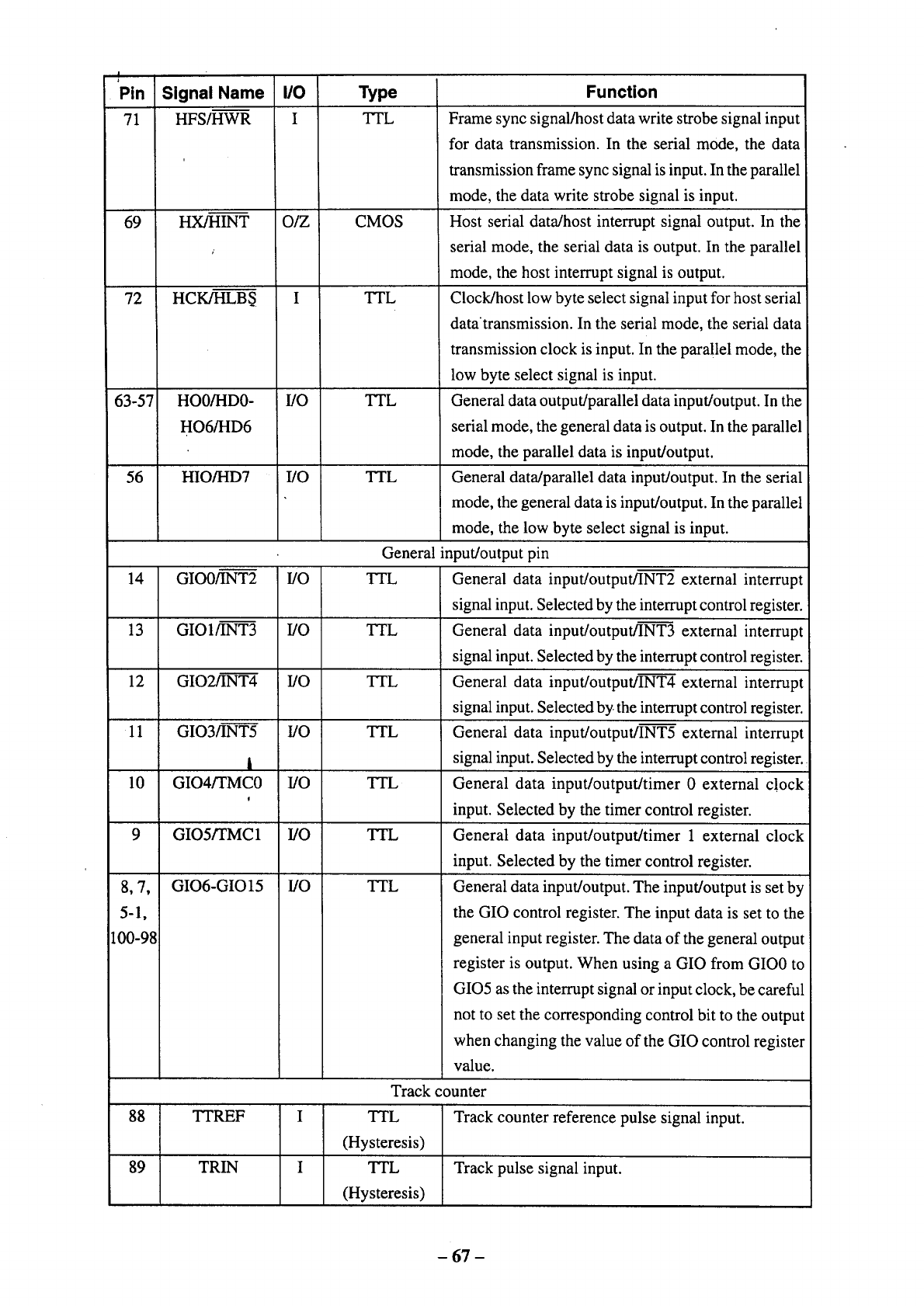
!Pin
71
69
72
63-57
56
Signal Name
HFS/HWR
HX/HINT
HCK/HLBS
HO0/HD0-
HO6/HD6
HIO/HD7
14 GIO0/INT2
13 GIO1/INT3
12 GIO2/INT4
Function
Frame sync signal/host data write strobe signal input
for data transmission. In the serial mode, the data
transmission frame sync signal is input. In the parallel
mode, the data write strobe signal is input.
Host serial data/host interrupt signal output. In the
serial mode, the serial data is output. In the parallel
mode, the host interrupt signal is output.
TTL Clock/host low byte select signal input for host serial
datatransmission. In the serial mode, the serial data
transmission clock is input. In the para!lel mode, the
low byte select signal is input.
TTL General data output/parallel data input/output. In the
serial mode, the general data is output. In the parallel
mode, the parallel data is input/output.
TTL General data/parallel data input/output. In the serial
mode, the general data is input/output. In the parallel
mode, the low byte select signal is input.
General input/output pin
TTL General data input/output/INT2 external interrupt
signal input. Selected by the interrupt control register.
TTL General data input/output/INT3 external interrupt
signal input. Selected by the interrupt control register.
TTL General data input/output/INT4 external interrupt
signal input. Selected by.the interrupt control register.
TTL General data input/output/INT5 external interrupt
signal input. Selected by the interrupt control register.
TIL General data input/output!timer 0 external clock
input. Selected by the timer control register.
TTL General data input/output/timer 1external clock
input. Selected by the timer control register.
TTL General data input/output. The input/output is set by
the GIO control register. The input data is set to the
general input register. The data of the general output
register is output. When using a GIO from GIO0 to
GIO5 as the interrupt signal or input clock, be careful
not to set the corresponding control bit to the output
when changing the value of the GIO control register
value.
Track counter
Track counter reference pulse signal input.
I/O
I
O/Z
I/O
I/O
lJO
I/O
I/O
11 GIO3/INT5 I/O
|
10 GIO4/TMC0 I/O
i
9 GIO5/TMC 1 I/O
8, 7_
5-1,
100-98
GIO6-GIO15 I/O
88 TTREF
TRIN89
Type
TTL
CMOS
TTL
(Hysteresis)
TTL
(Hysteresis)
Track pulse signal input.
- 67 -
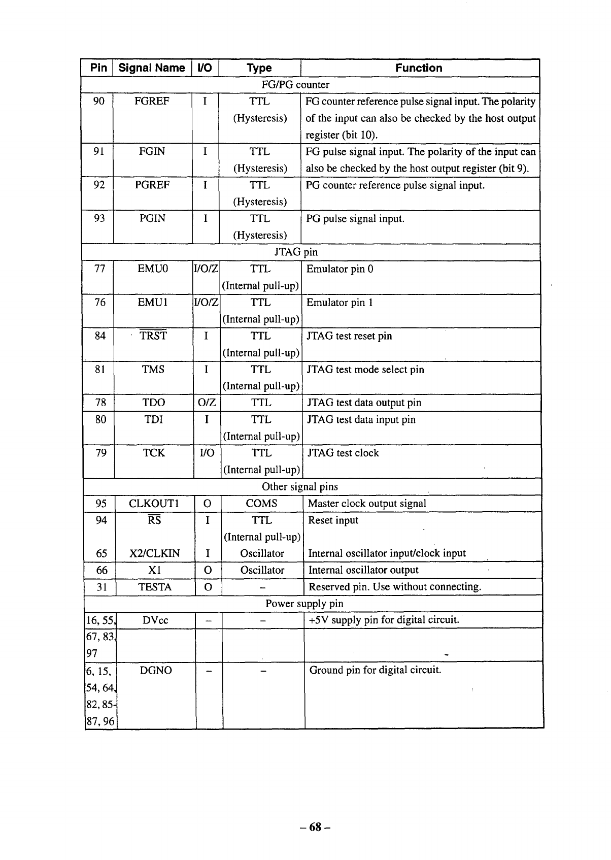
Pin I Signa,Name Ivol
90 FGREF I
91 FGIN I
92 PGREF I
93 PGIN I
77
76
84
81
EMU0 IIO/Z
EMU1 I/O/Z
TRST I
TMS I
78 TDO O/Z
80 TDI I
79 TCK I/O
95
94
CLKOUT1 O
RS I
Type
FG/PG counter
TTL
(Hysteresis)
65
66
31
16,55.
67,83
97
6,15,
54,64,
82,85-
87,961
X2/CLKIN I
Xl O
TESTA O
DVcc
DGNO
TTL
(Hysteresis)
TTL
(Hysteresis)
TTL
(Hysteresis)
JTAG
TTL
(Internal pull-up)
TTL
(Internal pull-up)
TTL
(Internal pull-up)
TTL
(Internal pull-up)
TTL
TTL
(Internal pull-up)
TTL
(Internal pull-up)
Function
FG counter reference pulse signal input. The polarity
of the input can also be checked by the host output
register (bit 10).
FG pulse signal input. The polarity of the input can
also be checked by the host output register (bit 9).
PG counter reference pulse signal input.
PGpulse signal input.
pin
Emulator pin 0
Emulator pin 1
JTAG test reset pin
JTAG test mode select pin
JTAG test data output pin
JTAG test data input pin
JTAG test clock
Other signal pins
Master clock output signal
Reset input
COMS
TTL
(Internal pull-up)
Oscillator
Oscillator
Internal oscillator input/clock input
Internal oscillator output
- Reserved pin. Use without connecting.
Power supply pin
- +5V supply pin for digital circuit.
- Ground pin for digital circuit.
- 68 -
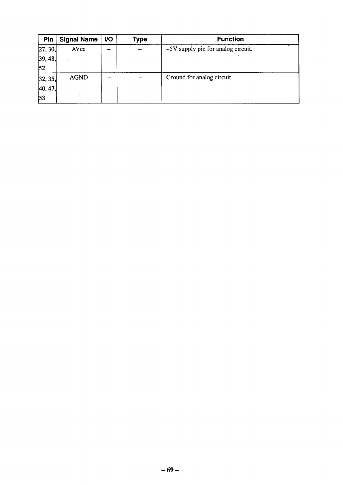
Pin
27, 30,
39, 48,
52
32, 35,
40, 47,
53
Signal Name I/0
AVcc
AGND
Type Function
+5V supply pin for analog circuit.
Ground for analog circuit.
- 69 -
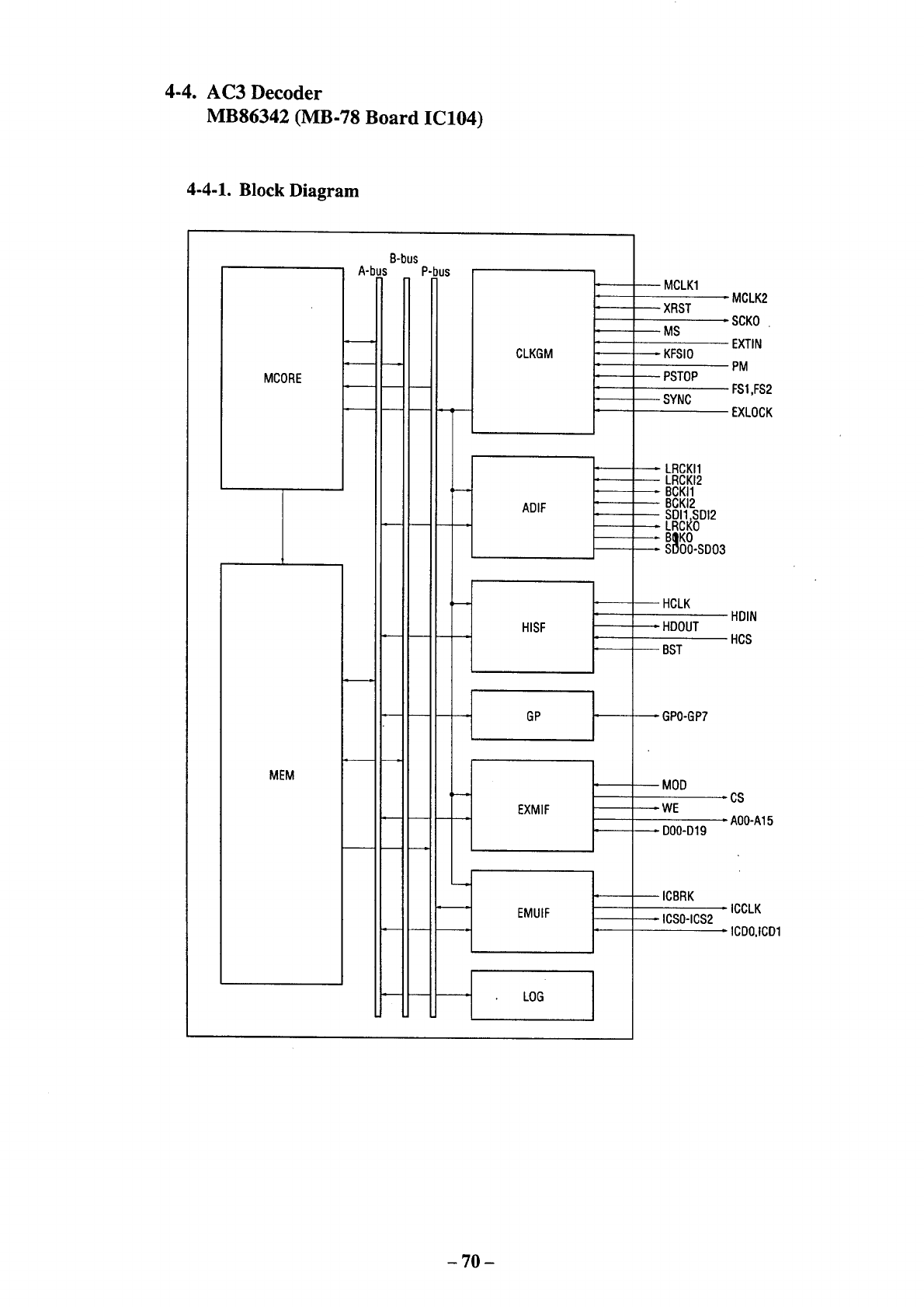
4-4. AC3 Decoder
MB86342 (MB-78 Board IC104)
4-4-1. Block Diagram
MCORE
MEM
B-bus
/_-OLIS
U
_'.DUS
CLKGM
ADIF
HISF
GP
EXMIF
EMUIF
LOG
-- MCLK1 MCLK2
-- XRST SGKO
- -- MS EXTIN
•- _ KFSlO PM
-- PSTOP FS1,FS2
-- SYNC EXLOCK
LRCKI1
-- LRCKI2
BCKI1
-- BCKI2
- -- SDII,SDI2
LRCKO
_B_KO
SDOO-SD03
-- HCLK -HDIN
HDOUT
"HCS
-- BST
.... GPO-GP7
--MOD
-CS
._ WE AOO-A15
DOO-D19
--ICBRK ICCLK
._ICSO-ICS2 -ICDO,ICD1
-70 -
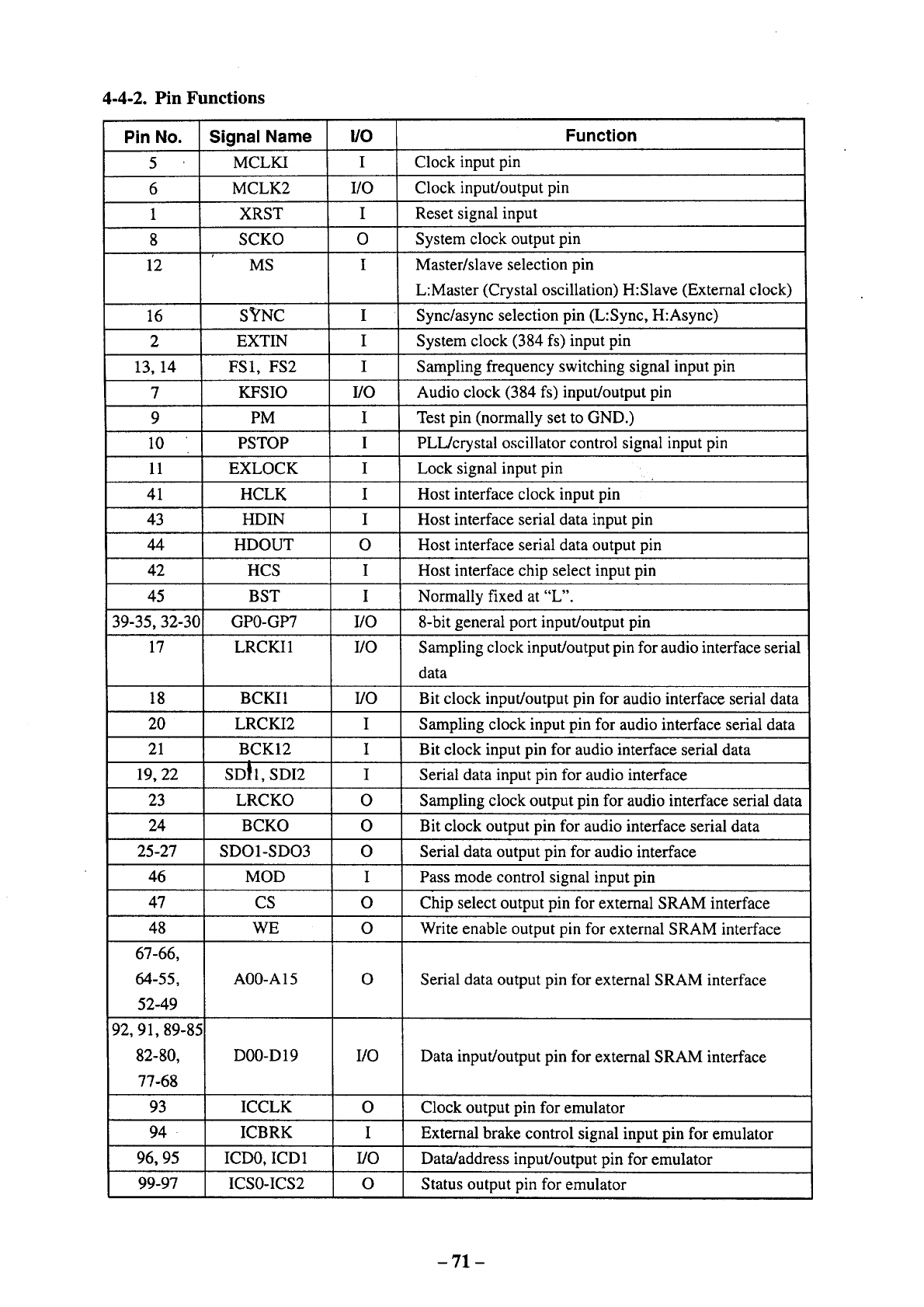
4-4-2. Pin Functions
Pin No.
5
6
Signal Name
MCLKI
MCLK2
1 XRST
8 SCKO
12 MS
16
2
13, 14
7
9
10
11
41
43
44
42
45
39-35, 32-30
17
18
20
21
19, 22
23
24
25-27
46
47
48
67-66,
64-55,
52-49
92, 91, 89-85
82-80,
77-68
93
94
96, 95
99-97
S_NC
EXTIN
FS1, FS2
KFSIO
PM
PSTOP
EXLOCK
HCLK
HDIN
HDOUT
HCS
BST
GP0-GP7
LRCKI1
BCKI1
LRCKI2
BCK12
SD_I, SDI2
LRCKO
BCKO
SDO1-SDO3
MOD
CS
WE
A00-A 15
D00-D19
ICCLK
ICBRK
ICD0, ICD 1
ICS0-ICS2
I/O
I
I/O
I
O
I
I
I
I
I/O
I
I
I
I
I
O
I
I
I/O
I/O
I/O
I
I
I
o
o
o
I
o
o
O
I/O
o
I
I/O
o
Function
Clock input pin
Clock input/output pin
Reset signal input
System clock output pin
Master/slave selection pin
L:Master (Crystal oscillation) H:Slave (External clock)
Sync/async selection pin (L:Sync, H:Async)
System clock (384 fs) input pin
Sampling frequency switching signal input pin
Audio clock (384 fs) input!output pin
Test pin (normally set to GND.)
PLL/crystal oscillator control signal input pin
Lock signal input pin
Host interface clock input pin
Host interface serial data input pin
Host interface serial data output pin
Host interface chip select input pin
Normally fixed at "L".
8-bit general port input/output pin
Sampling clock input/output pin for audio interface serial
data
Bit clock input/output pin for audio interface serial data
Sampling clock input pin for audio interface serial data
Bit clock input pin for audio interface serial data
Serial data input pin for audio interface
Sampling clock output pin for audio interface serial data
Bit clock output pin for audio interface serial data
Serial data output pin for audio interface
Pass mode control signal input pin
Chip select output pin for external SRAM interface
Write enable output pin for external SRAM interface
Serial data output pin for external SRAM interface
Data input/output pin for external SRAM interface
Clock output pin for emulator
External brake control signal input pin for emulator
Data/address input/output pin for emulator
Status output pin for emulator
-71 -
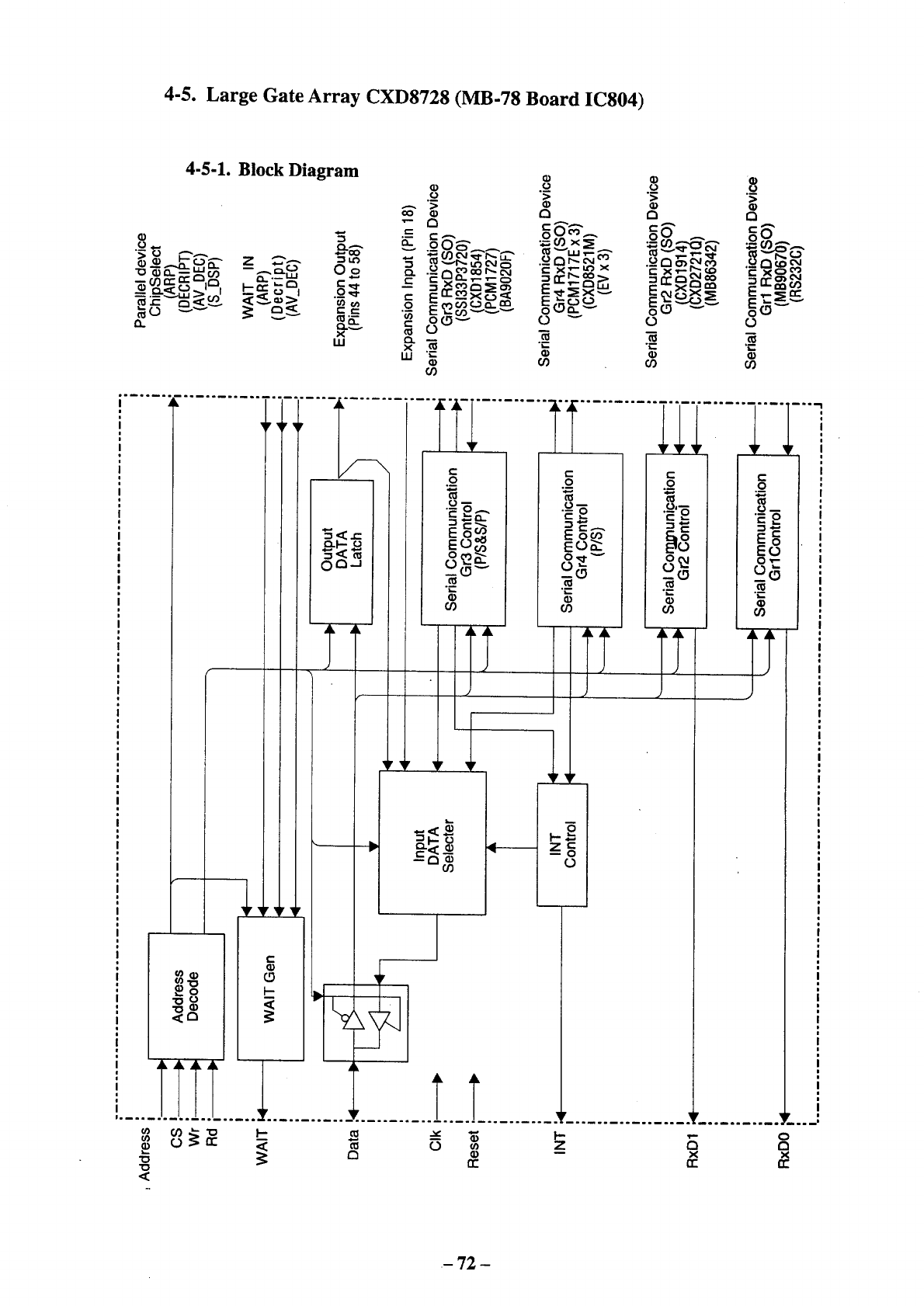
4-5. Large Gate Array CXD8728 (MB-78 Board IC804)
4-5-1. Block Diagram
oO
T,-
"5 .---
t_
3 o ,----
--=_w -- Oo
_, O0 t_ u: ,..%t-_ 0...:-'- ,.._
_o _ ""._= .-
0. _-_×
.£
>
0
N
co
.o_ .o_ .£
> > >
a a
..,rr_.N>=x---_ "_x_
_" ¢_X _ _- _.= _ t_--
0 v 0 0
og og o)
-72 -
4-5-2. Pin Functions
Pin No.
I
2
3
4
Signal Name
VDD
DVDLDONn
CDLDONn
CDfDVD
RD/WR,SHIF
I/O, RD/WR
I/O, RD/WR
I/O, RD/WR
5 OPN/CLS I/O, RD/WR
6 DRERR I/O, RD
7 NSTn I/O, RD/WR
8 SPCTL1 I/O, RD/WR
9 SPCTL0 I/O, RD/WR
10 SPGC2 I/O, RD/WR
11 DETON I/O, RD/WR
(Tout)
12 ACDDET I/O, RD
13 TILT/H I/O, RD/WR
14 BUS_2 I/O, RD
15 ERROR I/O, RD
i
(TIN)
16 LOCK I/O, RD
17 FOK I/O, RD
18 TRAYFREE I/O, RD/WR
19 S 12VOFF I/O, RD/WR
20 VDD
21 GND
22 SPGC 1 I/O, RDAVR
23 TBLR I/O, RD/WR
24 TBLL I/O, RD/WR
25 LDOUTn I/O, RD/WR
26 LDINn I/O, RD/WR
27 ACHUCK I/O, RD
28 ATRAY I10, RD
Function "
VDD
DVD laser light/off signal:ON when "L"
CD laser light/off signal:ON when "L"
Signal differentiating between CD and DVD:DVD
when "H".
Tray open/close. Open at "H" and Close at "L". Stop
when "Hiz".
DIR LC89051V error signal. Error when "H".
Spindle motor non-control voltage input.
Stop when set to 0V.
Switches the spindle servo operation mode.
Can be set to control, non-control, acceleration.
Switches the operation mode between SPCTL 1 and
2Bit.
Can be set to control, non-control, acceleration.
Spindle servo gain control signal.
Switches the gain of the "post stage" amplifier.
CD/DVD differentiation sensor ON/OFF SW
signal:ON when "H"
(Data output during memory test)
CD/DVD differentiation signal (sensor output
which is waveform-shaped)
TILT servo characteristics switching signal
Servo DSP busy flag:Busy when "L"
Servo DSP error flag:Error when "L"
(clk signal input during the memory test)
From ARP
From DSP
Releases the tray driver. Open when "L".
Servo 12V power supply OFF. 12V on when "H"
VDD
GND
Spindle servo gain control signal.
Switches the gain of the "first stage" amplifier.
Changer roulette rotation. Rotates when "H".
Changer roulette rotation. Rotates when "H".
Changer loading OUT. Loading out when "L".
Changer loading IN. Loading in when "L".
Mechanism chucking detection signal.
"H" when chucking.
Tray open signal. "H" when the tray is open.
- 73 -
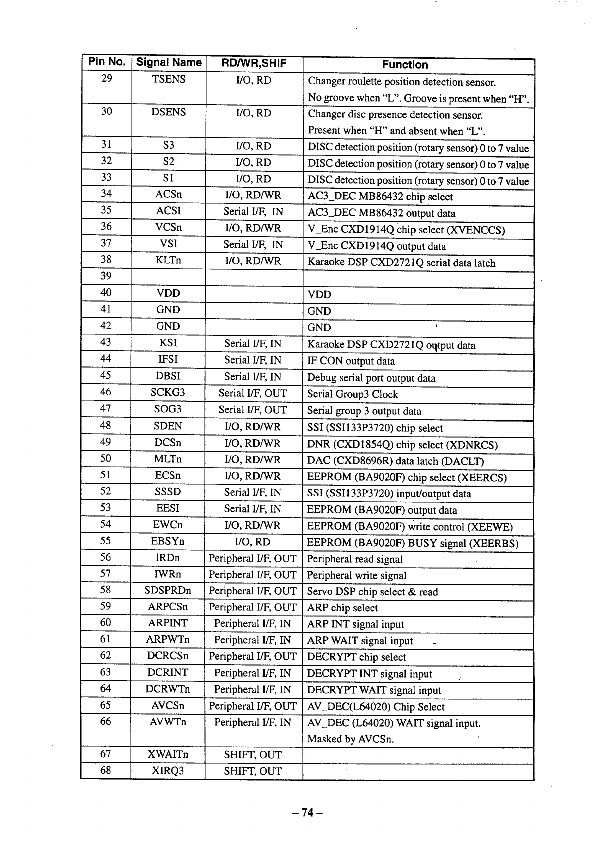
Pin No.
29
30
31
32
33
34
35
36
37
38
39
40
41
42
43
44
45
46
47
48
49
50
51
52
53
54
55
56
57
58
59
6O
61
62
63
64
65
66
67
" 68
Signal Name
TSENS
DSENS
$3
$2
S1
ACSn
ACSI
VCSn
VSI
KLTn
VDD
GND
GND
KSI
IFSI
DBSI
SCKG3
SOG3
SDEN
DCSn
MLTn
ECSn
SSSD
EESI
EWCn
EBSYn
IRDn
IWRn
SDSPRDn
ARPCSn
ARPINT
ARPWTn
DCRCSn
DCRINT
DCRWTn
AVCSn
AVWTn
XWAIT'n
XIRQ3
RD/WR,SHIF
I/O, RD
I/O, RD
I/O, RD
I/O, RD
I/O, RD
I/O, RD/WR
Serial I/F, IN
I/O, RD/WR
Serial I/F, IN
I/O, RD/WR
Serial I/F, IN
Serial I/F, IN
Serial I/F, IN
Serial I/F, OUT
Serial I/F, OUT
UO, RD/WR
I/O, RD/WR
I/O, RD/WR
I/O, RD/WR
Serial I/F, IN
Serial I/F, IN
I/O, RD/WR
I/O, RD
Peripheral I/F, OUT
Peripheral I/F, OUT
Peripheral I/F, OUT
Peripheral I/F, OUT
Peripheral I/F, IN
Peripheral I/F, IN
Peripheral I/F, OUT
Peripheral I/F, IN
Peripheral I/F, IN
Peripheral I/F, OUT
Peripheral I/F, IN
SHIFT, OUT
SHIFT, OUT
Function
Changer roulette position detection sensor.
No groove when "L". Groove is present when "H".
Changer disc presence detection sensor.
Present when "H" and absent when "L".
DISC detection position (rotary sensor) 0 to 7 value
DISC detection position (rotary sensor) 0 to 7 value
DISC detection position (rotary sensor) 0 to 7 value
AC3_DEC MB86432 chip select
AC3_DEC MB86432 output data
V_Enc CXD1914Q Chip select (XVENCCS)
V_Enc CXD1914Q output data
Karaoke DSP CXD2721Q serial data latch
VDD
GND
GND
Karaoke DSP CXD2721Q oqtput data
IF CON output data
Debug serial port output data
Serial Group3 Clock
Serial group 3 output data
SSI (SSI133P3720) chip select
DNR (CXD 1854Q) chip select (XDNRCS)
DAC (CXD8696R) data latch (DACLT)
EEPROM (BA9020F) chi p select (XEERCS)
SSI (SSI133P3720) input/output data
EEPROM (BA9020F) output data
EEPROM (BA9020F) Write control (XEEWE)
EEPROM (BA9020F) BUSY signal (XEERBS)
Peripheral read signal
Peripheral write signal
Servo DSP chip select & read
ARP chip select
ARP INT signal input
ARP WAIT signal input ..
DECRYPT chip select
DECRYPT INT signal input
DECRYPT WAIT signal input
AV_DEC(L64020) Chip Select
AV_DEC (L64020) WAIT signal input.
Masked by AVCSn.
- 74 -
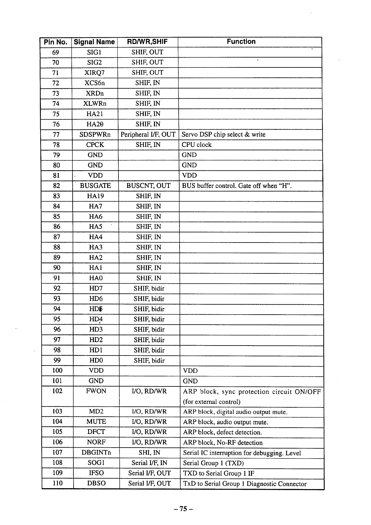
Pin No.
69
70
71
72
73
74
75
76
77
78
79
80
81
82
83
84
85
86
87
88
89
90
91
92
93
94
95
96
97
98
99
100
101
102
Signal Name
SIG1
SIG2
XmQ7
XCS6n
XRDn
XLWRn
HA21
HA20
SDSPWRn
CPCK
GND
GND
VDD
BUSGATE
RD/WR,SHIF
SHIE OUT
SHIE OUT
SHIF, OUT
SHIE IN
SHIE IN
SHIE IN
SHIE IN
SHIE IN
Peripheral I/F, OUT
SHIE IN
BUSCNT, OUT
HA19 SHIE IN
HA7 SHIF, IN
HA6
HA5
HA4
HA3
HA2
HA1
HA0
HD7
HD6
HDI_
HD4
!
HD3
HD2
HD1
HD0
VDD
GND
FWON
SHIE IN
SHIF, IN
SHIF, IN
SHIF, IN
SHIF, IN
SHIF, IN
SHIF, IN
SHIF, bidir
SHIF, bidir
SHIF, bidir
SHIF, bidir
SHIF, bidir
SHIF, bidir
SHIF, bidir
SHIF, bidir
Function
Servo DSP chip select & write
CPU clock
GND
GND
VDD
BUS buffer control. Gate off when "H".
VDD
GND
I/O, RD/WR ARP block, sync protection circuit ON/OFF
(for external control)
103 MD2 I/O, RD/WR ARP block, digital audio output mute.
104 MUTE I/O, RD/WR ARP block, audio output mute.
105 DFCT I/O, RD/WR ARP block, defect detection.
106 NORF I/O, RD/WR ARP block, No-RF detection
107 DBGINTn SHI, IN Serial IC interruption for debugging. Level
108 SOG1 Serial I/F, IN Serial Group 1 (TXD)
109 IFSO Serial I/F, OUT TXD to Serial Group 1 IF
110 DBSO Serial I/F, OUT TxD to Serial Group 1 Diagnostic Connector
- 75 -
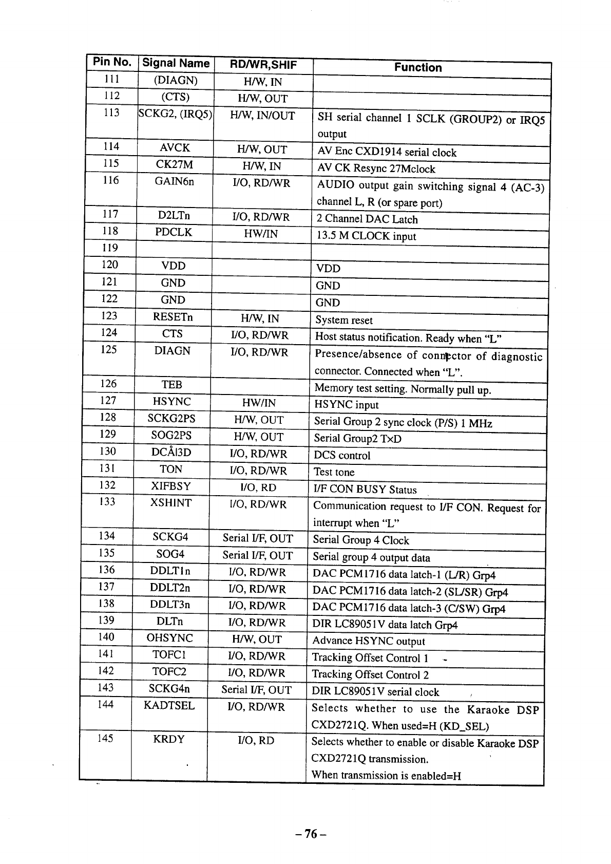
Pin No.
111
112
113
114
115
116
117
118
119
120
121
122
123
124
125
126
127
128
129
130
131
132
133
134
135
136
137
138
139
140
141
142
143
144
145
Signal Name
(DIAGN)
(CTS)
SCKG2, (IRQ5)
AVCK
CK27M
GAIN6n
D2LTn
PDCLK
VDD
GND
GND
RESETn
CTS
DIAGN
TEB
HsYNc
SCKG2PS
SOG2PS
DC/_I3D
TON
xIFBSY '
XSHINT
SCKG4
SOG4
DDLT 1n
DDLT2n
DDLT3n
DLTn
OHSYNC'
TOFC 1
TOFC2
scKG4n
KADTS'EI_
KRDY
RD/WR,SHIF
H/W, IN
H/W, OUT
H/W, IN/OUT
H/W, o'UT
" 'H/W, IN
I/O, RD/WR
I/O, RD/wR
HW/IN
H/W, IN
UO, RD/WR
I/O, RD/WR
HW/IN
H/W, OUT
H/W, OUT
I/O, RD/WR
I/O, RD/WR
I/0, RD
....I/O, RD/WR
Serial I/F, OUT
Serial I/F, OUT
I/O, RD/WR
' I/O, RD/WR
frO, RD/WR
I/O, RD/WR
H/W, OUT
I/O, RD/WR
I/O, RD/WR
Serial I/F, OUT
I/O, RD/WR
Function
SH serial channel I SCLK (GROUP2) or IRQ5
output
AV Enc CXD1914 serial clock
AV CK Resync 27Mclock
AUDIO output gain switching signal 4 (AC-3)
channel L, R (or spare port)
2 Channel DAC Latch
13.5 M CLOCk input
VDD
GND
GND
System reset
Host status notification. Ready when "L"
Presence/absence Of connector of diagnostic
connector. Connected when "L".
Memory test setting. Normally pull up.
HSYNC input
Serial Group 2 sync clock (P/S) 1 MHz
Serial Group2 TxD
DCS control
Test 'tone
I/F CON BUSY Status
Communication request to I/F CON. Request for
interrupt when "L"
Serial Group 4 Clock
Serial group 4 output data
DAC PCM1716 data latch-I (L/R) Grp4
DAC PCM1716 data latch-2 (SL/SR) Grp4
DAC PCM17 i6 data latch-3 (C/SW) Grp4
DIR LC89051V data latch Grp4
Advance HSYNC output
Tracking'Offset Control 1 -
Tracking Offset Control 2
DIR LC89051V serial clock
Selects whether to use the Karaoke DSP
CXD2721Q. When used=H (KD_SEL)
Selects whether to enable or disable Karaoke DSP
CXD2721Q transmission.
When transmission is enabled=H
I/0, RD
-76-
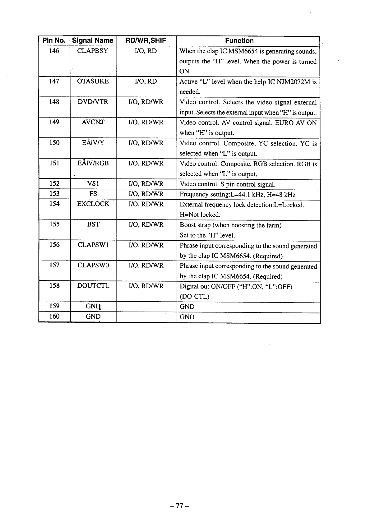
Pin No.
146
147
148
149
150
151
152
153
154
155
156
157
158
159
160
Signal Name
CLAPBSY
OTASUKE
DVD/VTR
AVCNT
EAIV/Y
E/_IV/RGB
VS1
FS
EXCLOCK
BST
CLAPSW1
CLAPSW0
DOUTCTL
GNq
GND
!
RD/WR,SHIF
I/O, RD
I/O, RD
I/O, RD/WR
I/O, RD/WR
I/O, RD/WR
I/O, RD/WR
I/O, RD/WR
I/O, RD/WR
I/O, RD/WR
I/O, RD/WR
I/O, RD/WR
I/O, RD/WR
I/O, RD/WR
Function
When the clap IC MSM6654 is generating sounds,
outputs the "H" level. When the power is turned
ON.
Active "L" level when the help IC NJM2072M is
needed.
Video control. Selects the video signal external
input. Selects the external input when "H" is output.
Video control. AV control signal. EURO AV ON
when "H" is output.
Video control. Composite, YC selection. YC is
selected when "L" is output.
Video control. Composite, RGB selection. RGB is
selected when "L" is output.
Video control. S pin control signal.
Frequency setting:L=_. 1 kHz, H=48 kHz
External frequency lock detection:L=Locked.
H=Not locked.
Boost strap (when boosting the farm)
Set to the "H" level.
Phrase input corresponding to the sound generated
by the clap IC MSM6654. (Required)
Phrase input corresponding to the sound generated
by the clap IC MSM6654. (Required)
Digital out ON/OFF ("H":ON, "L":OFF)
(DO-CTL)
GND
GND
- 77 -
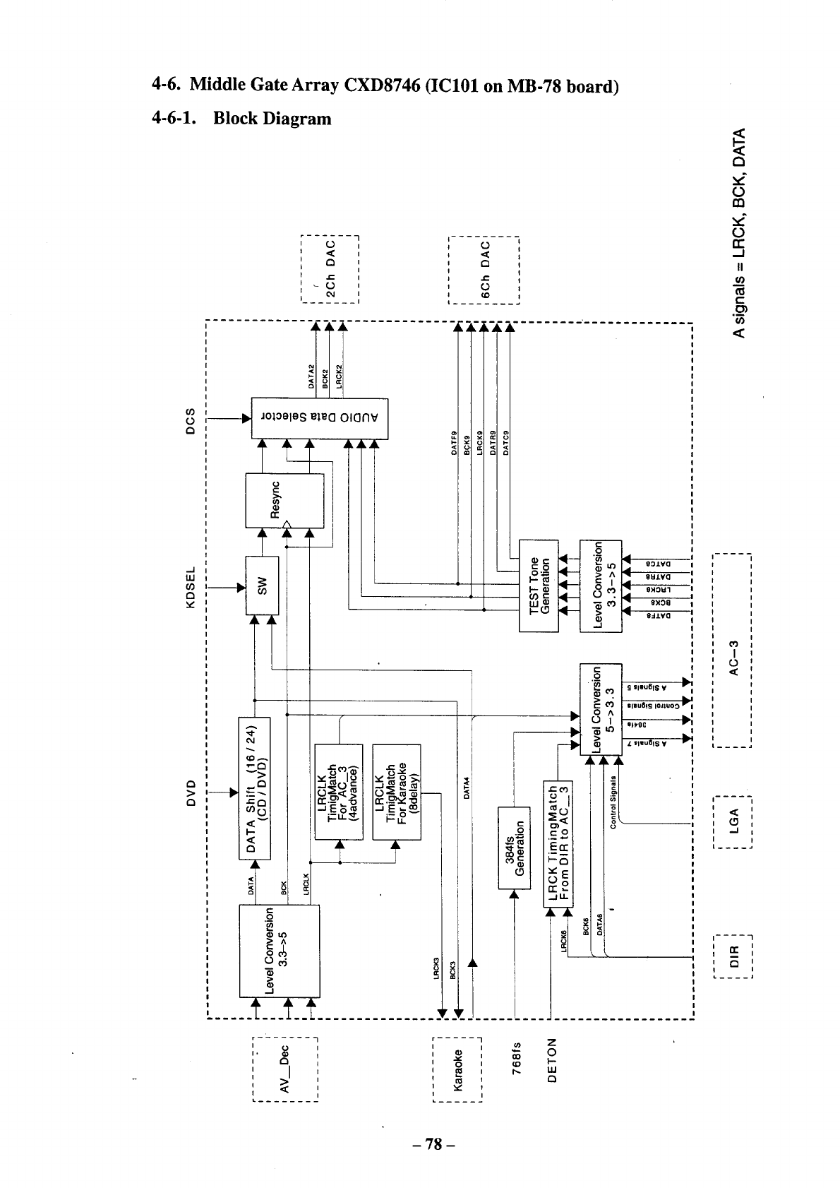
4-6. Middle Gate Array CXD8746 (IC101 on MB-78 board)
4-6-1. Block Diagram
o
<
o
r-
/
t..o _ Joloele£ e_.eO olanv
o i/
Q
..... .t_..t..t. ._:
(,3
<
a
.C
O
CD
o :- i..--
.._ a a
83ZVO
/_ u:,_: _ >- ^ I "q 8u.l.Va
I _-_ __..1 _ i 1_
. / I _ _ O":L,, 6,ou',
a
o
rn
0
n-
II
0)
<
o
i
i
I
SWlIIU61S VP'_mI
€_lUU6!_ lO,qUOO r!
':'Tii•
t .... _
I
' .... 1
' I
I
z
o
-78 -
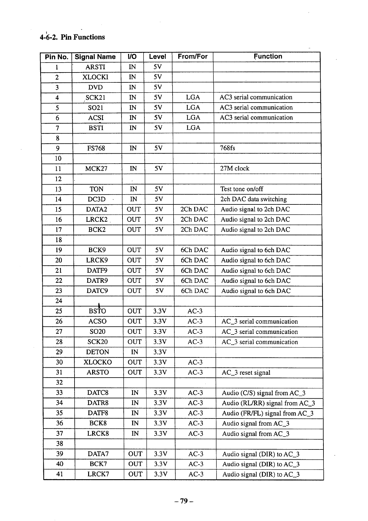
!
4-6-2. Pin Functions
Pin No. Signal Name
1 ARSTI
2 XLOCKI
3 DVD
4 SCK21
5 SO21
6 ACSI
m
7 BSTI
8
9 FS768
10
11 MCK27
12
13 TON
14 DC3D
15 DATA2
16 LRCK2
17 BCK2
18
19 BCK9
20 LRCK9
21 DATF9
22 DATR9
23 DATC9
24 t
25 BSTO
26 ACSO
27 SO20
28 SCK20
29 DETON
30 XLOCKO
31 ARSTO
32
33 DATC8
34 DATR8
35 DATF8
36 BCK8
37 LRCK8
38
39 DATA7
40 BCK7
41 LRCK7
I/0
IN
IN
IN
IN
IN
IN
IN
IN
IN
IN
IN
OUT
OUT
OUT
OUT
OUT
OUT
OUT
OUT
OUT
OUT
OUT
OUT
IN
OUT
OUT
IN
IN
IN
IN
IN
OUT
OUT
OUT
Level
5V
5V
5V
5V
5V
5V
5V
5V
5V
5V
5V
5V
5V
5V
5V
5V
5V
5V
5V
3.3V
3.3V
3.3V
3.3V
3.3V
3.3V
3.3V
3.3V
3.3V
3.3V
3.3V
3.3V
3.3V
3.3V
3.3V
From/For
LGA
LGA
LGA
LGA
2Ch DAC
2Ch DAC
2Ch DAC
6Ch DAC
6Ch DAC
6Ch DAC
6Ch DAC
6Ch DAC
AC-3
AC-3
AC-3
AC-3
AC-3
AC-3
AC-3
AC-3
AC-3
AC-3
AC-3
AC-3
AC-3
AC-3
Function
AC3 serial communication
AC3 serial communication
AC3 serial communication
768fs
27M clock
Test tone on/off
2ch DAC data switching
Audio signal to 2ch DAC
Audio signal to 2ch DAC
Audio signal to 2ch DAC
Audio signal to 6ch DAC
Audio signal to 6ch DAC
Audio signal to 6ch DAC
Audio signal to 6ch DAC
Audio signal to 6ch DAC
AC_3 serial communication
AC_3 serial communication
AC_3 serial communication
AC_3 reset signal
Audio (C/S) signal from AC_3
Audio (RL/RR) signal from AC_3
Audio (FR/FL) signal from AC_3
Audio signal from AC_3
Audio signal from AC_3
Audio signal (DIR) to AC_3
Audio signal (DIR) to AC_3
Audio signal (DIR) to AC_3
- 79 -
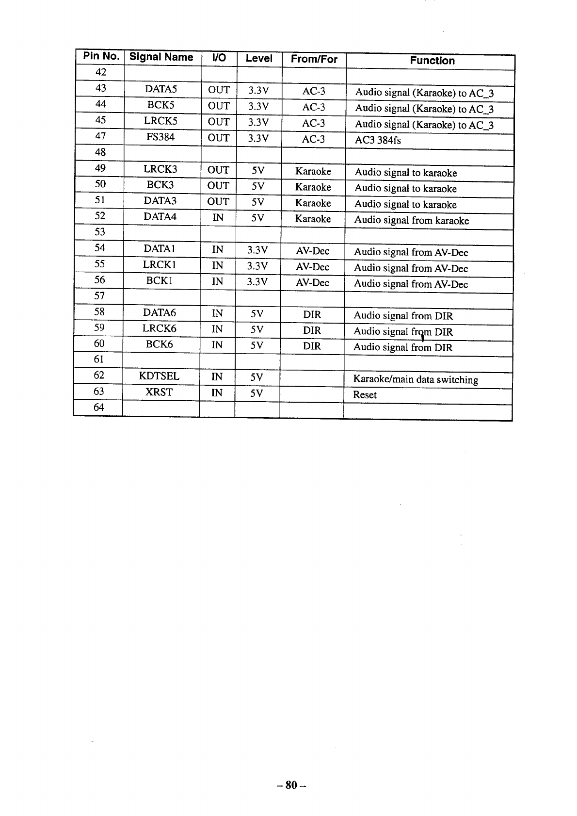
From/For Function
Pin No.
42
43
44
45
47
48
49
50
51
52
53
54
55
56
57
58
59
60
61
62
63
64
Signal Name
DATA5
BCK5
LRCK5
FS384
LRCK3
BCK3
DATA3
DATA4
DATA1
LRCK1
BCK1
DATA6
LRCK6
BCK6
KDTSEL
XRST
I/O
OUT
OUT
OUT
OUT
OUT
OUT
OUT
IN
IN
IN
IN
IN
IN
IN
IN
IN
Level
3.3V
3.3V
3.3V
3,3V
5V
5V
5V
5V
3.3V
3.3V
3.3V
5V
5V
5V
5V
5V
AC-3
AC-3
AC-3
AC-3
Karaoke
Karaoke
Karaoke
Karaoke
AV-Dec
AV-Dec
AV-Dec
DIR
DIR
DIR
Audio signal (Karaoke) to AC_3
Audio signal (Karaoke) to AC_3
Audio signal (Karaoke) to AC_3
AC3 384fs
Audio signal to karaoke
Audio signal to karaoke
Audio signal to karaoke
Audio signal from karaoke
Audio signal from AV-Dec
Audio signal from AV-Dec
Audio signal from AV-Dec
Audio signal from DIR
Audio signal fr_rn DIR
Audio signal from DIR
Karaoke/main data switching
Reset
- 80 -
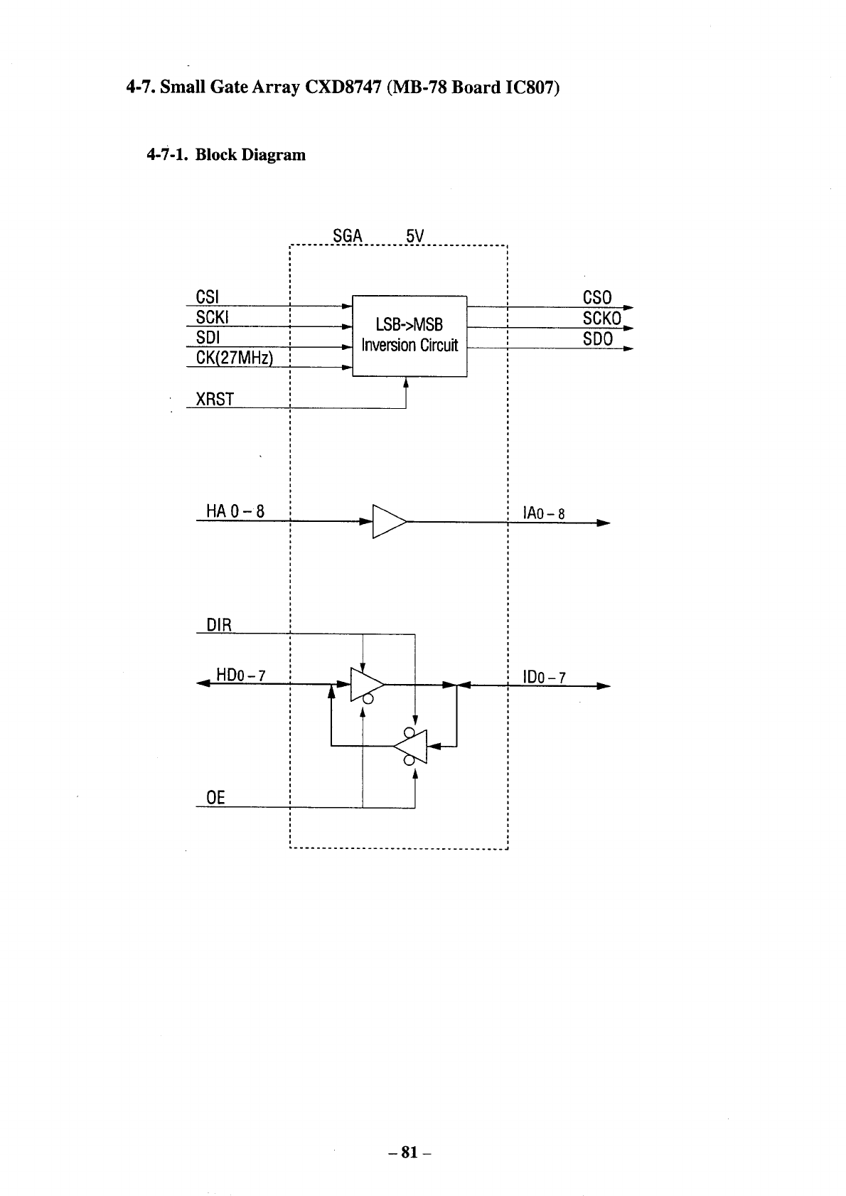
4-7. Small Gate Array CXD8747 (MB-78 Board IC807)
4-7-1. Block Diagram
SGA 5V
CSI _l
SCKI ! i
', LSB->MSB
SDI ! InversionCircuit
CK(27MHz) i,
XRST
HA 0 -8
DIR
HDo-7
OE
CSO
SCKO
,
i
:SDO
IAO- 8
i,,.
v
IDo-7
-81 -
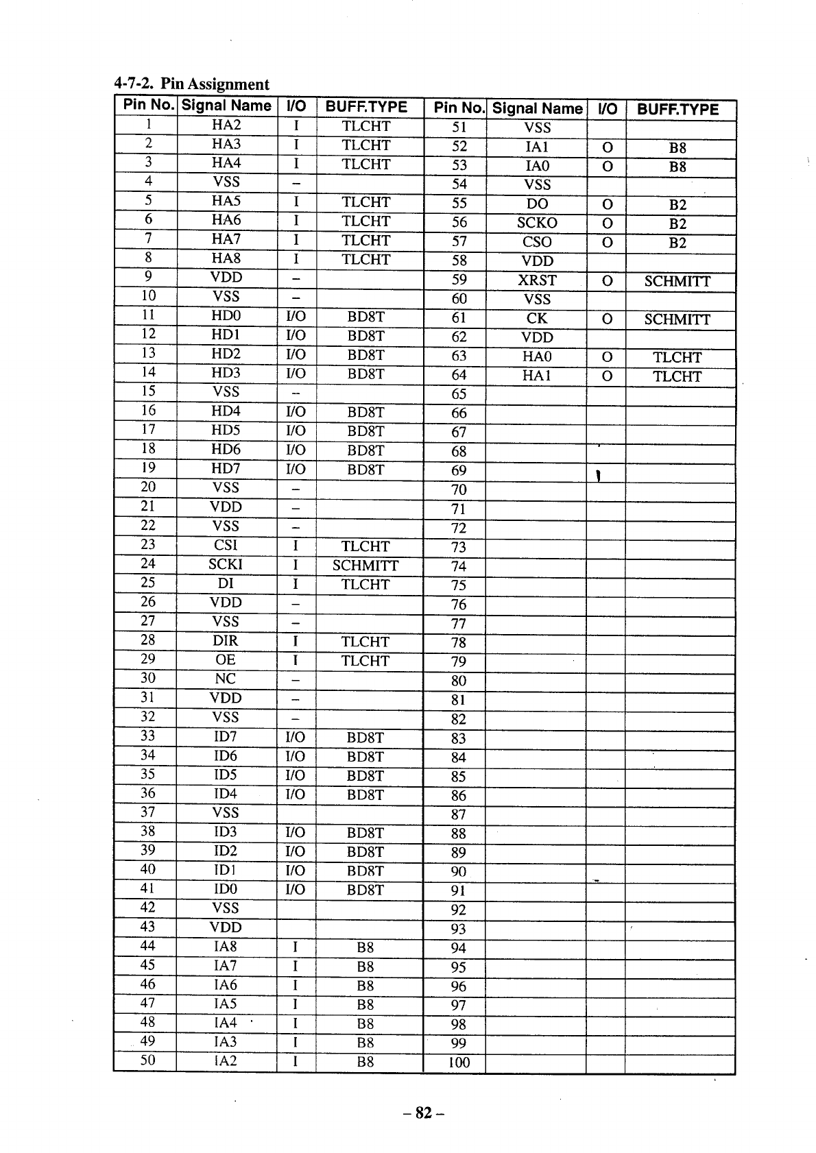
4-7-2. Pin Assignment
Pin No.
I
2
3
4
5
6
7
8
9
i0
II
12
13
14
15
16
17
18
19
20
21
22
23
24
25
26
27
28
29
30
31
32
33
34
35
36
37
38
39
40
41
42
43
44
45
46
47
48
49
50
Signal Name
HA2
HA3
HA4
VSS
HA5
HA6
HA7
HA8
VDD
VSS
HD0
HD1
HD2
HD3
VSS
HD4
HD5
HD6
HD7
VSS
VDD
VSS
CSI
SCKI
DI
VDD
VSS
DIR
OE
NC
VDD
VSS
ID7
ID6
ID5
ID4
VSS
ID3
ID2
ID1
ID0
VSS
VDD
IA8
IA7
IA6
IA5
IA4
IA3
IA2
I/0
l
!
T
T
I
T
I
BUFF.TYPE
TLCHT
TLCHT
TLCHT
TLCHT
TLCHT
TLCHT
TLCHT
BD8T
BD8T
BD8T
BD8T
I/O
I/O
I/O
I/O
UO BD8T
I/O BD8T
I/O BD8T
I/O BDST
I TLCHT
I SCHMITT
I TLCHT
I TLCHT
1 TLCHT
I/O BD8T
I/O BD8T
I/O BD8T
I/O BD8T
I/O BD8T
I/O BD8T
I/O BD8T
I/O BD8T
I B8
I B8
I B8
I B8
I B8
I B8
1 B8
Pin No.
51
52
53
54
55
56
57
58
59
60
61
62
63
64
65
66
67
68
69
70
71
72
73
74
75
76
77
78
79
8O
81
82
83
84
85
86
87
88
89
9O
91
92
93
94
95
96
97
98
99
100
Signal Name I/0 BUFF.TYPE
VSS
IA1 O B8
IA0 O B8
VSS
DO O B2
SCKO O B2
CSO O B2
VDD
XRST OSCHMITT
VSS
CK 0 SCHMITT
VDD
HA0 O TLCHT
HA1 OTLCHT
- 82 -
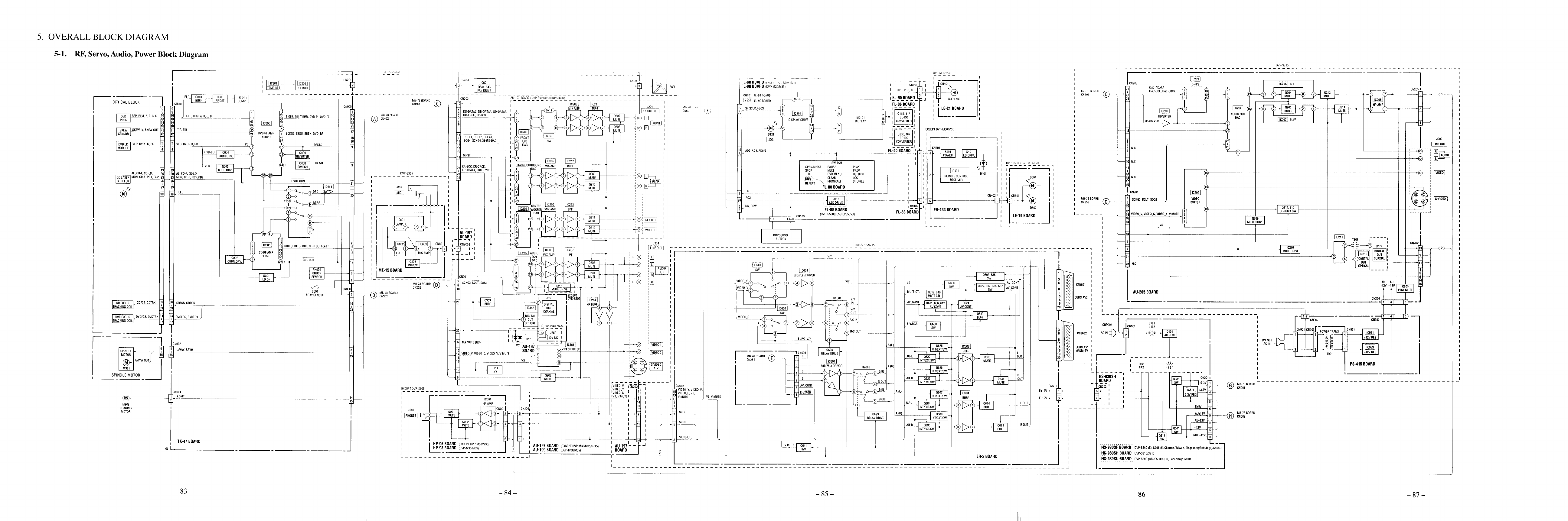
5 OVERALL BLOCK DIAGRAM
5-1. RF, Serve, Audio, Power Block Diagram
........... r I' £'10"; 'uVP M30 MJt'
f ..................................................... '........ _c_
' _ _ 9I 1._b.I _ 4\_ FAN ; EL-{}' I}OARD ,1 ,CN1Olr. 'pLCN4Ol ' -"
' . _ / vz_._: , Dvow_.cDJl_ IL %,_-_
- --- ,oF_..J__ _ _ _o,L _-,BOOARO10,_O, ..... rA_I_A_'_O_'O_'_DY............................................... 1........ ' C"'O2:EL-00SOAROi----_0!'0_ _ I_'_-,0_BO_A._oL'_J] i-Y °'_°_ I
OmlOALBLOOK :NOOll r _ IIc,_o, © " _ r , _oo= ,_,j 1 ' I
CN005 J2o IML' :' ,--, /FL-88 BOARD
7 9 1{ MIXAMP BUFF ' '_' _ " 8" _ "1 I I II
D TIOFS TIE TIERR DVD PI OVO FE 3 1iI I
CN402 ...... d @, [3_
-6'3 ,@ , ,ND,01 46 L ---
' -- ....... --- "................ -- 10 '- ........ _" " _: I
II ; ,_1 /1 _",'fl D,SPLA¥OR,VeT_ 14o_ °,SPLAY _II_,I4_FT1_o_%1m ....... "
I--_E_--IsKEw'NSKEW0utl;, t,AtIB _ ;_ [I_1 I I H / ,I '_ "_ _..._>_ :,,X i_',_, / _P_ l.)_t- %J I I ;--------.--4 EXCEPTOVP-_O,M;D
IsE,so,I ' I, -- ....... -- _i OVORFAMP",qSOKG3,SSSD,SBEN,DVOBF+ / I','1 J I BI .... / I I ICl_03JI _ I--L.--I I" I _ ', I / 012,/ _2 _ I III 0106,107]I I..........
I- "r SERVO 145 -- TqmF-q I.I BDLTI.ODLT2. BDLT3. / I (_ FRONT I_L)2_°_ [ ' '
_VLD, DVD-LD,PU I VLD, DVD-LD, PD POA- _ DFCTS I _ J _;'_I _-_-4d_,_l _'_cl _' _ -" _ , '
OVD-LD. ,MRS, ,' ' ' f - T T ,tT,I'F _ _
TILT/H I , I | OPEN/CLOSE PAUSE PLAY r -- / J I I I J _ \-_;l _ 2 +__ T,LT__I _ I _,R-BC,,_R-ORDN,/ /1____ ' r 4 :, , 1/SdTC, ,//',11 f_
r_Vl T _ I _ ! II I t 11'IKR-ADATA,384FS-2CH//I ,£_'-I DAcF-----I _ _ I ' ', ,/ / I SlOP NEXT PREV I I []_,LI I 1104ol1 IiT-
ALCD-FCD-LD, I; ALCD-FCD-LD -- I L _ _ I/I I I DVPS3O5 _gq_ .... Q l ] [ , I'J _ ,.-_1"_ .Ph..&P'._ .4-. I _pn_ ]I'_'_ ' // I TITLE DVDMENU RETURN I_ 4 4']_tt21.- J_r._n_,[, .... ID401
_MON. CD-E,Pm.P021i,, , , _ ......M_N,CB'-E..........PDt'PD2 . __ I _ / I I t r ................ _ IEI / / / I'_1_'1 __/_1 _r_; _ --,'t2J,IL______ I / / I i[ji_r:- CLEAR ,JOG I i F_I'_ _ ............... I DSO_
_qi - L_ I I OVDL_N _ . _ _ ' i _ I _ I I I _ I I L[ l LI _ I ,, ,_ l'| I "R[p-['AT_PROGRAM SHUFFLE I=iI'.11iI RECE,VERi "Y
_. | LeD I _Q-..._,@PD SWTCH| _ I _ /_IT ] I I '||_Iz'_l '_ _ _-_-J I ' I L,. _ l _--- ,rli:ll , i
-- E ..... i '=_ 2:: i [ I l AC3 / 1..... _ _ /K I I " CN402 CN5OlI ."_"
t;w.oow !- - ,_ .... ,--LI',,U-" -- O _ >4__
i i _-- _ 'Y t II I ' Ifi_ ---r_ I', I / I I I' ,c___ _" _ :..... I CN10..02_I I ID502
.... ' ' ' I" I t ,'-B,BOA,D ......... I FR-133BOARD/
II_' 111II _I! _--_-I B_Cr-z--i F_I _ i, , I (BVD-SSOOB/S501D/S505D) r_-oo ou_nu II
// II I,,I I,, / ,c.o - ,,.o.,.o -
-- - -11=1 14+.oI-- ...... ,..... ,
'II : ; i
T II I,,I 4 /
, _ _ : -_:, -4@',l_oo_Rj
. I BOAR., ............. ,
..... -- i/COO1] [/] t I _ N.C
II I , AUDIO I -- FI
I I ' _ _JI I
, -- , ' , , V,BEO_1 _.o-_ _-" w / / J vs _-=-_F AVCONTT1/ I1_°11
// _ _1_t_ _ ......... M;;B;,_;_--_._BO0' ] _ I _L=_=J____'_L:=_J._lt _ _ , -
ov..ovo.J .............. = = . - '
I ' I I I I
III l H _ana_ian. model [ ]_ i II I --_T I
I _ ' ,II
,_ _1 [_-_'*' .... _-1 _n_s_ i l I I I .... ,
..... r -- -q - , , IONJ602 I
[- 7, I I I : : ,
J. Ac,oo= I I ] r_'_IMAMUTE(NO)-'s_-__T_..J I 1 ,_® [_J', L___ _Eo___ Lq>____J I..I I I I I --IIo°_11 '
_ _ U/V/W. SPVR _-j _DEO V. VIBEO C. VIDEO_Y. VMUT£ .......... _OA'_D_ _. -:--__{_ i_ II [ _;-,,_-_,._TC----_°_qlJl_ I II_l_' _q'"'_=;"__ _' ' _l_uTJi I_III°-_iI'°N°Av''(RGB)fV II
...... , ] S VIDEO I
,,, ,, ' I_ o,,_,v_,___G2fRY602 A(R] AUL.R_ _,_.
LH2- .i II:o.o, ,o , _ _ONT 1_1 ' 1i _ "1 '_ ' I _ I ="_'_ ' DN5011 )i--
NO04 EX.CEP_TP__V_S 30_.5...... £ ........ q_ -_ iiii_-_: _D. EO-v' L_ E-V,_ A,L,I I--"n'_n_---] ' _ | ,,,1,V _, I...
f_'L 111 LDMT h,d 'r"-------"---_l . . L_ ., , 'VS, VMOTE' .2 VMUTE VS, V MUTE [. L___ ___ _'-_ AU!_.[ ____L OUT _1 =
MgB2 t | HP AMP / /
LOAD,_ ' T .... ' _ r---ncNoo,,_,o,, r l I: ,_, |
MOTOR .... _ , - ''' I AU-L
._ -- ,, -- _ ............... _ ROUT
t_-,,BOARD , _ _ _ 4: _ -_,d " _ _UTE:€_,_L _ ................................. '
..,BOA.D,EXOEPTBVP-_,O,_,,, ' " _i'-
HP 98 BOARD (DVPM30/M35) IAU-197 BOARD (EXOEPTDVP-M30/M35/S715) AU-1B7--
05 "- J AU-199BOARD (DVP-M30/M35) BOARD
FL-90BOARD (BVDM30/M35)
MB-78 BOARD
CNlOl] FL-88 BOARD CNI01
MB-TB BOARD
0N252
EXCEPT DVP-M3_M35
AD3, AD4, AD5_
DVP-SbUUI;, boo it),bbOJ U
(DVD-S5OOD/S501DtSSO5D)
DVPS115
CN203 D-FFS
F OAOAOAFA4_ 4'-
@ g._ OAO-BC_.OAC-LRO_, ,1'1
I R
1_ N.C
13
15 N.B
CN201
SCKG3. D2LT, SOG3
..... _ VIDEO_V. VIDEO_C. VIDEO_Y, V MUTE •
VS
__
AU-205 BOARD
%1-_N1B,'
ON tl_
.s.,_os.', Ffl ]-,-_ I oN.,,
BOARD ; / / fl %' _+.v --(_) D,OO,
c;_oT' , / / I '-:F-' ,._L__,'_=. _ MB-_BBOARD
_-_ ---t / I I I,_P _
' '// III ,.,v.
--. , . Ao+,_v ...._._"_;;_oO_RD
iHS-93OSF BOARD : BVP-S30B (E), S305 (E, Chinese, Taiwan, Sinoapore)iS5OOO (E)/S505q
: HS-93OSUBOARD:DVP-S30B (US)/S5OOD (US, Canadian)!S5OlD /
J
J
@
T201 I
AU AU
+12V -12V
CN204
,_ CN9O2 CN952
AC IN _ T901 J "_
P8-415 BOARD
!
LE
TT,
1
CN2O5 I
t 41_ .
J202
- 83- - 84- - 85- - 86- - 87 -
II
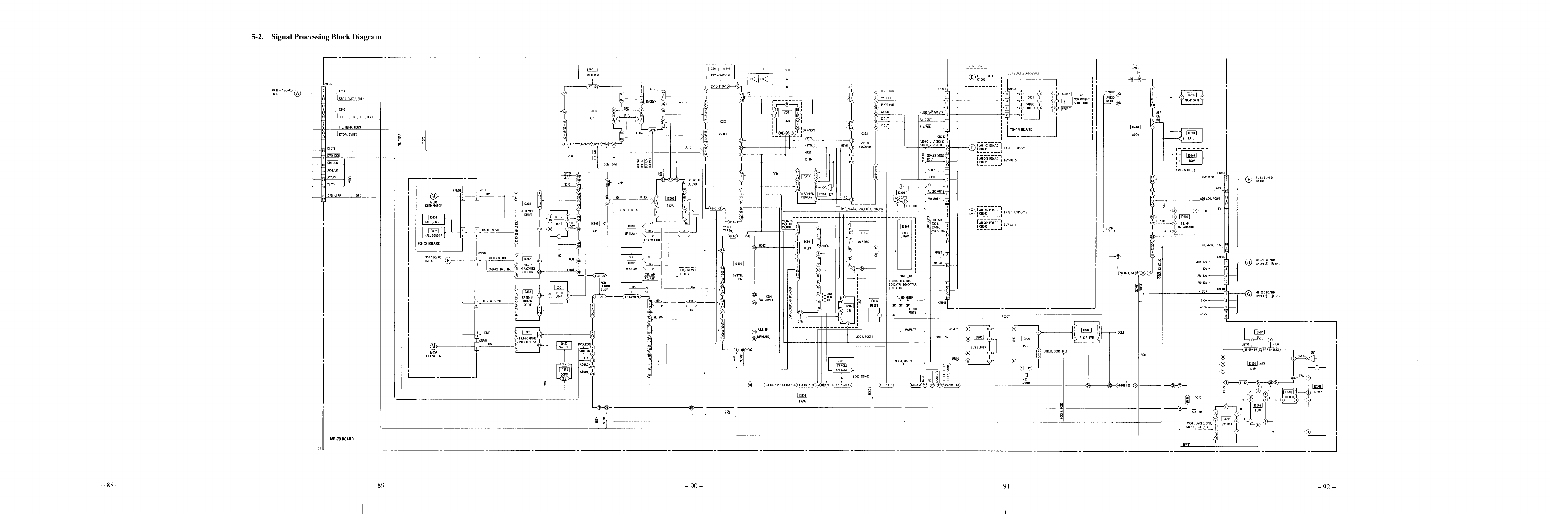
5-2. Signal Processing Block Diagram
I0 1K-47 BOARD
CN005 _
ION542
DVD RF
_DEN
CDRF
_,CDTE, TEATT
TIE,TIERR, TIOFS
-L_DVDPI, DVDFE
DFCTS
DVDLDON
AUHUCK ]
BPD, MIRR DPD
MB-78 BOARD
I
Im2DliL'C2D2i
16MX2 SDRAM
AV DEC
SRST
LG/A
'blJl
;MHz
t DVP 50UOD_bD0/U/_00DU ----
,®=-2OOAOD:, __
CN603 I I I I
I J I I I
I , • I
H[I,_ Zi_, ,r-, [COMPONENT_I
I]u_LE_2J I
B-V,"GB ,'_ 1 i!
__ , YS-._OARO I I
0N252 1 I .... _ IpCON
r5 iJ
VIDEO V, VIDEO C
VIDEO-Y VMUTE l&l _=_ i AU-197BOARD I
•._- '"I;_-_U).,=. ,vI0N201 ,I EXCEPT DVP-S715
i/sot_o.,soo=_Ir--:--:- ',
=_Io_ Ik_l I IAU-2OSBOARD,DVPS715
>_!.!_ LCN_Dj.... i "
Ir-- I';'_U)_ I CN203 IEXCEPTDVP-S715
F_-_FBOATB-'.......
ICNIO3 I UVP'-bLID
-..()
(_ BUS BUFF,R (_ PLL //
SCKG3, SOG3, _
i
i
ALE
I I
I I
DVP-SS00D (E) CN601
I" CW, CCW ----_-"-_ CN101IL'8IIUAHU
AC3
AD3,AD4, AD516
l__ FLcRs -I
ISI,SCLK, CNOO2 _J
-88- - 89 - - 90 - -91 - -92 -
k l
SONY,
