Sony FF031021 GSM/GPRS 850/1800/1900 Module User Manual
Sony Mobile Communications Inc GSM/GPRS 850/1800/1900 Module
UserManual.wiki
>
Sony
>
FF031021 User Manual
User Manual
Navigation menu
Upload a User Manual
Namespaces
Wiki Guide
HTML
PDF
Info
Views
User Manual
Discussion / Help
Navigation
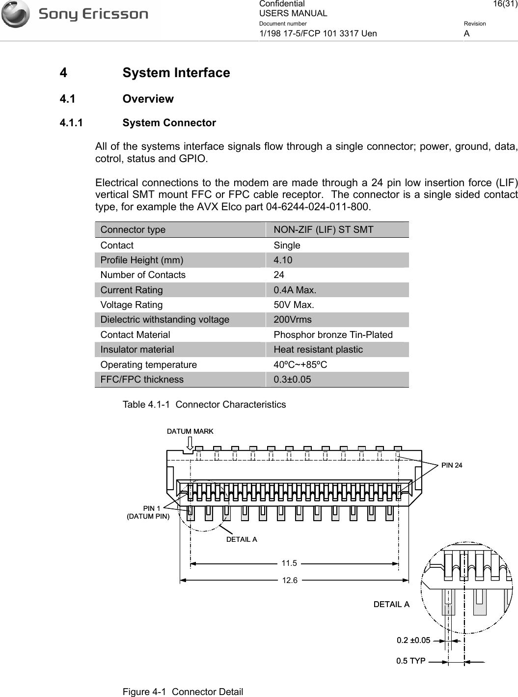
![Confidential USERS MANUAL 19(31)Document number Revision 1/198 17-5/FCP 101 3317 Uen A 5 Electrical Interface This section describes each signal line of the electrical interface between the EDGE modem and the host equipment application. A summary of the function of each signal is provided, together with any additional relevant information. Signals are described from the perspective of the EDGE modem and Daughter Card circuitry. Consequently signals described as input are inputs to the modem, driven by the host [host⇒modem]. Likewise, signals described as output are driven by the modem in to the host [modem⇒host]. Bi-directional signal flow (I/O) is indicated by a double-headed arrow [modem⇔host]. In some instances the [daughter card] will be identified if the modem circuitry is not directly involved, or where additional interface circuitry resides between the host and the modem. Signals which are pulled internally are identified in parentheses beside the signal name as either (PU)=Pulled Up or (PD)=Pulled Down. Signals with no designation are not pulled either way. 5.1 Power Interfaces This section describes the power, ground, and other signals that control or indicate power states. • VIN • 3V3 • VREF • GND 5.1.1 VIN Function: Daughter card power supply Description: Primary voltage supply to switching regulator (5.5 to 20.0V). Pin Numbers: 14, 15, 16, 17, 18, 19 Signal Names: VIN [host⇒daughter card] If not used: Required Details: Power provided by the host will range from 5.5V minimum to a maximum 20.0V, dependent upon the battery discharge state. The Daughter Card has on board regulation which regulates the supply range to a steady 3.6V by means of a switching regulator rated at 3A max.](https://usermanual.wiki/Sony/FF031021/User-Guide-517072-Page-19.png)
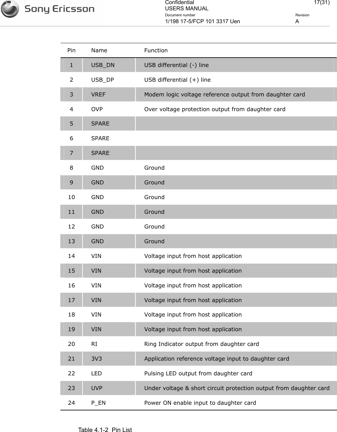
![Confidential USERS MANUAL 21(31)Document number Revision 1/198 17-5/FCP 101 3317 Uen A 5.1.2 3V3 Function: Daughter card reference voltage Description: Host reference to protection circuit & USB (3.3V) Pin Numbers: 21 Signal Names: 3V3 [host⇒daughter card] If not used: Required Details: The host supplies a 3.3V regulated supply to the Daughter Card for two primary functions: • reference supply for the undervoltage / short circuit protection circuitry • input for the USB interface Electrical Characteristics: Parameter Condition Min Nom Max Unit Voltage 3.30 V Ripple 100 mV 5.1.3 VREF Function: Voltage Reference Description: Core digital voltage reference from modem. Pin Number: 3 Signal Name: VREF [modem⇒host] If not used: Required Details: VREF is supplied as a reference voltage from the modem. This reference is the modem’s core digital supply voltage at a nominal 2.80V. The interface is capable of sourcing 200uA and is intended primarily for situations where host interface circuitry is required to be level shifted to maintain wireless modem signal level compatibility. If more current is required by the host, a current amplifier must be implemented.](https://usermanual.wiki/Sony/FF031021/User-Guide-517072-Page-21.png)
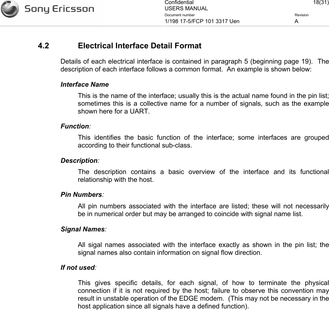
![Confidential USERS MANUAL 23(31)Document number Revision 1/198 17-5/FCP 101 3317 Uen A 5.2 Status Interfaces Status interfaces indicate or control status features of the modem. • UVP • OVP • RI • LED • VREF 5.2.1 UVP Function: Under voltage protection Description: Status indicator to host of potential malfunction in Daughter Card circuitry Pin Number: 23 Signal Name: UVP (PD) [daughter card⇒host] If not used: Required Details: The Daughter Card has FET circuitry which uses 3V3 as a reference, driving an output to the host indicating the voltage condition of the of VBAT (the modem supply voltage). A resistive divider connected to VBATT presents a very low Vbe to the UVP transistor. This presents a steady state low voltage output under normal VBAT conditions with external pulldown circuitry. In the event of a short circuit or high current fault condition on the Daughter Card, the voltage drop from the switching regulator will bias the UVP transistor on and present a high output to the host equipment monitoring circuit. The UVP signal should be pulled low by the application circuit for correct function. Electrical Characteristics: Parameter Condition Min Typ Max Unit Normal 0.5 V UVP output voltage Fault 3.3 V Table 5.2-1: UVP Electrical Characteristics](https://usermanual.wiki/Sony/FF031021/User-Guide-517072-Page-23.png)
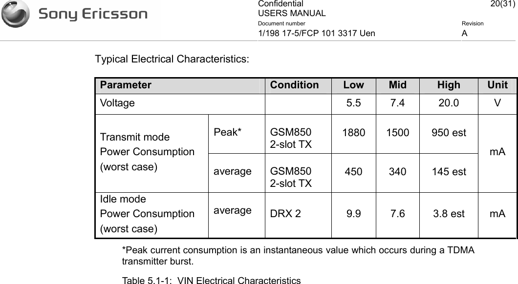
![Confidential USERS MANUAL 24(31)Document number Revision 1/198 17-5/FCP 101 3317 Uen A 5.2.2 OVP Function: Over voltage protection Description: Status indicator to host of potential malfunction in Daughter Card circuitry Pin Number: 4 Signal Name: OVP (PU) [daughter card⇒host] If not used: Required Details: The OVP signal is simply an output from the main onboard regulator. In it’s operational state under normal functional conditions this will output 3.6V nominal Parameter Condition Min Typ Max Unit Normal 3.6 V UVP output voltage Fault 3.7 V Table 5.2-2: OVP Electrical Characteristics 5.2.3 RI Function: Ring Indicator Description: Alert signal from the modem to indicate an incoming SMS, or unmasked unsolicited response Pin Number: 20 Signal Name: RI [modem⇒host] If not used: Leave open Details: Ring Indicator is essentially a wake-up call from the modem to the host application to signal one of two events: • an in-coming message (SMS). • an unmasked unsolicited response/result code. For the EDGE modem the Ring Indicator is implemented as a GPIO interface within the EDGE baseband device.](https://usermanual.wiki/Sony/FF031021/User-Guide-517072-Page-24.png)
![Confidential USERS MANUAL 25(31)Document number Revision 1/198 17-5/FCP 101 3317 Uen A A falling edge indicates an alert or message. The signal remains low for a period of time before going high. An SMS-page or unsolicited response/result code generates one pulse (the length is configurable using an AT command)[TBC]. The ring indicator is implemented on the daughter card as an open collector transistor output to allow the host the convenience of driving the host equipment circuitry. 5.2.4 LED Function: LED Description: LED-signal indicating a status change Pin Number: 22 Signal Name: LED [modem⇒host] If not used: Leave open Details: The LED is implemented on the Daughter Card as an open collector transistor output which providesa driver level interface to an LED acting as a status indicator for the user. The LED output can be made to blink at a rate pre-determined by modem software. 5.2.5 VREF The function of VREF is already described in 5.1.3. This interface can be used as a status indicator to the host that the modem is still powered. VREF is present whilst the modem is powered and is removed upon the completion of the modem power down. This feature can be useful in the event of a communications lock-up between the host and the daughter card.](https://usermanual.wiki/Sony/FF031021/User-Guide-517072-Page-25.png)
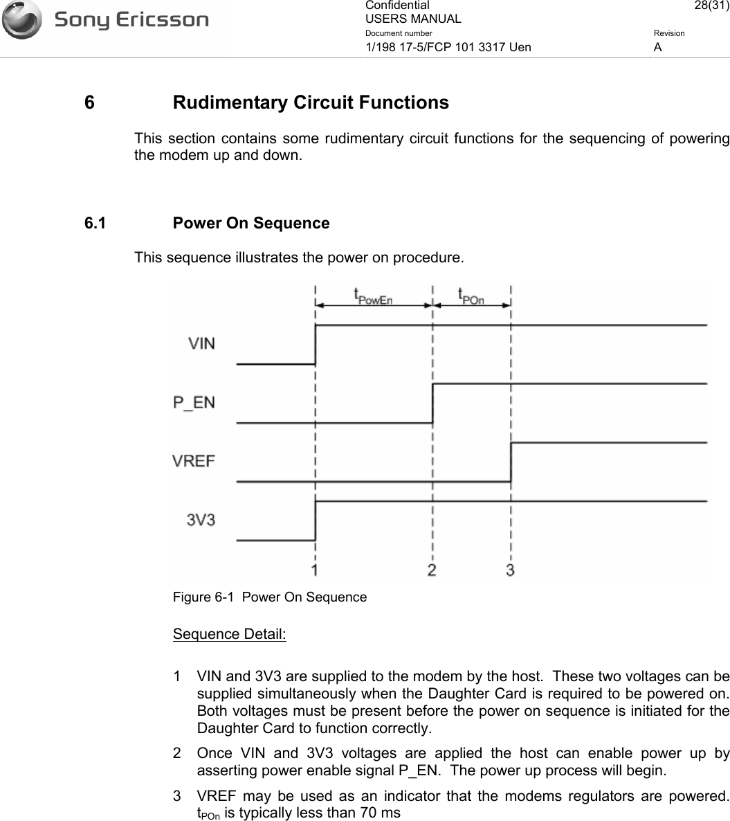
![Confidential USERS MANUAL 26(31)Document number Revision 1/198 17-5/FCP 101 3317 Uen A 5.3 Data Communication and Control Interfaces The serial data and control interfaces consist of the following : • USB • P_EN 5.3.1 USB Interface Function: USB data communication port Description: USB transmit and receive port for data communication between modem and host. Pin Numbers: 1, 2 Signal Names: USB_DP (2) [modem⇔host] USB_DN (1) [modem⇔host] If not used: Required Details: Power to the USB interface is provided by the 3V3 input from the host. 5.3.2 P_EN Function: Power Enable Description: Modem power enable control from host Pin Numbers: 24 Signal Names: P_EN [host⇒daughter card] If not used: Required Details: The power enable signal is provided from the host application and is routed to the switching regulator shutdown input and also to the REG_EN (regulator enable) pin on the modem. Assertion of this pin will initiate power up. The P_EN pin is active high and has to be maintained continually in order to keep the modem powered.](https://usermanual.wiki/Sony/FF031021/User-Guide-517072-Page-26.png)