Sony FF031021 GSM/GPRS 850/1800/1900 Module User Manual
Sony Mobile Communications Inc GSM/GPRS 850/1800/1900 Module
Sony >
User Manual

Confidential
USERS MANUAL
1(31)
Document number Revision
1/198 17-5/FCP 101 3317 Uen A
Prepared by Date
SEM/BMDES RODNEY WILLIAMS 2005-02-17
Contents responsible if other than preparer Remarks
Approved by
SEM/BMDES (RODNEY WILLIAMS)
This document is managed in metaDoc.
Note: Any hard copy of this document is for reference only. Due to template and application dependencies the header and footer may fail to display correct data. It is
the responsibility of the user to ensure that they have a correct and valid version. Any outdated hard copy is invalid and must be removed from possible use.
EDGE Daughter Card User Manual
The information contained in this document is the proprietary information of Sony Ericsson
Mobile Communications International. The contents are confidential and any disclosure
to persons other than the officers, employees, agents or subcontractors of the owner or
licensee of this document, without the prior written consent of Sony Ericsson Mobile
Communications International, is strictly prohibited. Further, no portion of this
publication may be reproduced, stored in a retrieval system, or transmitted in any form or by
any means, electronic or mechanical, including photocopying and recording, without the
prior written consent of Sony Ericsson Mobile Communications International, the
copyright holder.
Sony Ericsson Mobile Communications International publishes this document without
making any warranty as to the content contained herein. Further Sony Ericsson Mobile
Communications International reserves the right to make modifications, additions and
deletions to this document due to typographical errors, inaccurate information, or
improvements to programs and/or equipment at any time and without notice. Such changes
will, nevertheless be incorporated into new editions of this document.
All rights reserved.
© Sony Ericsson Mobile Communications International, 2005

Confidential
USERS MANUAL
2(31)
Document number Revision
1/198 17-5/FCP 101 3317 Uen A
Contents
Part 1 : Overview...............................................................................................3
1 Introduction..........................................................................................4
1.1 Target Users........................................................................................5
1.2 Prerequisites........................................................................................5
1.3 Notation ...............................................................................................5
2 EDGE Wireless Modem.......................................................................6
2.1 EDGE Wireless Modem in a Communication System .........................6
2.2 Functional Block Diagram....................................................................8
2.3 Features ..............................................................................................9
2.3.1 Mobile Station Characteristics .............................................................9
2.3.2 Environmental Conditions..................................................................12
2.4 SIM Card ...........................................................................................12
2.5 Other Features ..................................................................................12
2.6 Precautions........................................................................................12
Part 2 : Daughter Card Description .................................................................13
3 Mechanical Description .....................................................................14
3.1 Physical Detail ...................................................................................14
4 System Interface................................................................................16
4.1 Overview............................................................................................16
4.1.1 System Connector .............................................................................16
4.2 Electrical Interface Detail Format.......................................................18
5 Electrical Interface .............................................................................19
5.1 Power Interfaces................................................................................19
5.1.1 VIN.....................................................................................................19
5.1.2 3V3 ....................................................................................................21
5.1.3 VREF .................................................................................................21
5.1.4 GND...................................................................................................22
5.2 Status Interfaces................................................................................23
5.2.1 UVP ...................................................................................................23
5.2.2 OVP ...................................................................................................24
5.2.3 RI .......................................................................................................24
5.2.4 LED....................................................................................................25
5.2.5 VREF .................................................................................................25
5.3 Data Communication and Control Interfaces.....................................26
5.3.1 USB Interface ....................................................................................26
5.3.2 P_EN .................................................................................................26
5.4 ANTENNA CONNECTOR .................................................................27
6 Rudimentary Circuit Functions ..........................................................28
6.1 Power On Sequence .........................................................................28
6.2 Power Off Sequence .........................................................................29
6.3 USB communications timing..............................................................29

Confidential
USERS MANUAL
3(31)
Document number Revision
1/198 17-5/FCP 101 3317 Uen A
Part 1 : Overview
Confidential
USERS MANUAL
4(31)
Document number Revision
1/198 17-5/FCP 101 3317 Uen A
1 Introduction
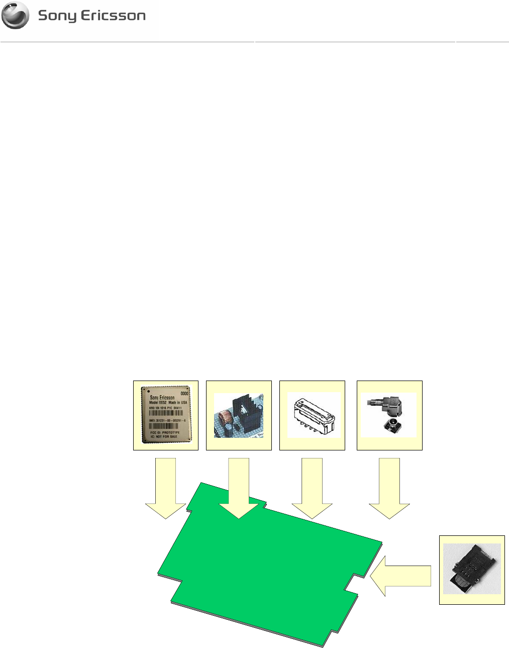
The EDGE Daughter Card product is a custom product, developed for the host equipment
customer.
The EDGE Daughter Card is a total solution designed as an add-in option for integrators
of the host equipment. The Daughter Card comprises of several component parts:
• EDGE wireless modem, which is the wireless enabling circuitry integrated on to the
Daughter Card PCB together with its mechanical RF shielding
• RF connector, which provides physical connectivity between the Daughter Card and
the antenna which is integrated in to the notebook mechanical housing
• Voltage regulation circuitry, which converts raw unregulated power from the host
battery to the core regulated voltage to the EDGE wireless components
• System connector, which provided the data, control, power and status interface
between the host and the wireless modem
• SIM connector, a combined connector and retention device for the users Subscriber
Identity Module (SIM) card
EDGE WIRELESS
CIRCUITRY
VOLTAGE
REGULATION
SYSTEM
CONNECTOR
RF ANTENNA
CONNECTOR
DAUGHTER
CARD
SIM
CONNECTOR
EDGE WIRELESS
CIRCUITRY
VOLTAGE
REGULATION
SYSTEM
CONNECTOR
RF ANTENNA
CONNECTOR
DAUGHTER
CARD
SIM
CONNECTOR
Figure 1-1 EDGE Daughter Card Component Parts

Confidential
USERS MANUAL
5(31)
Document number Revision
1/198 17-5/FCP 101 3317 Uen A
1.1 Target Users
The EDGE Daughter Card solution is specifically for the host equipment.
1.2 Prerequisites
Integration of the EDGE Daughter Card will be performed at facilities under the host
equipment customer’s management. All necessary integration instruction, driver software
and user documentation will be provided. No special pre-requisite knowledge is
necessary.
1.3 Notation
This document describes a custom solution for the host equipment. The Daughter Card
product is defined through a cooperative partnership between the host equipment
customer and Sony Ericsson Mobile Communications (SEMC).
EDGE (Enhanced Data rate for GSM Evolution) is the wireless-enabling technology.
The EDGE Daughter Card is a PCB assembly with the components described on the
previous page integrated on to the board. The complete assembly is reffered in this
document as the the host equipment DC (DC=Daughter Card ).
Confidential
USERS MANUAL
6(31)
Document number Revision
1/198 17-5/FCP 101 3317 Uen A
2 EDGE Wireless Modem
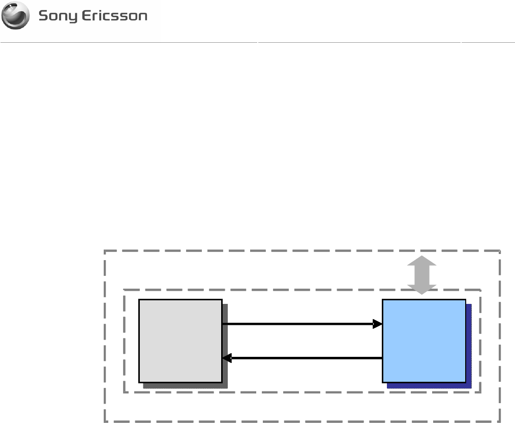
2.1 EDGE Wireless Modem in a Communication System
Figure 2-1 illustrates the main blocks of a wireless communication system using the
EDGE Daughter Card embedded in the host equipment device. It also shows the
communication principles of the system. The definitions in the figure, as used elsewhere
in this manual, are in accordance with the recommendations of GSM 07.07.
• The MS (mobile station) represents the EDGE Daughter Card modem plus SIM card.
• The modem excluding SIM card, is known as the ME (mobile equipment).
• The TE (terminal equipment) is a micro-controller and is a part of the application.
Figure 2-1 Main Blocks in a Wireless System
In accordance with the recommendations of ITU-T (International Telecommunication
Union - Telecommunications Standardisation Sector) V.24, the TE communicates with the
MS over a serial interface. In this case this is the Universal Serial Bus (USB).
The functions of the EDGE modem follow the recommendations provided by ETSI
(European Telecommunications Standards Institute) and ITU-T.
ETSI specifies a set of AT commands for controlling the GSM/E-GSM element of the
modem; these commands are supplemented by Sony Ericsson specific commands.
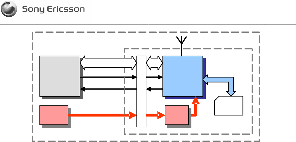
Figure 2-2 illustrates the interface between the Daughter Card and the the host equipment
application. Each interface signal is described in Section 3.
MS
(EDGE
MODEM)
TE
(DTE)
GSM Network
MS Status, responses
AT commands to control MS
Host Equipment
Wireless Communications System
MS
(EDGE
MODEM)
TE
(DTE)
GSM Network
MS Status, responses
AT commands to control MS
Wireless Communications System
Confidential
USERS MANUAL
7(31)
Document number Revision
1/198 17-5/FCP 101 3317 Uen A
TE
(DTE)
MS
(EDGE
MODEM)
SIM
Power
Power
SYSTEM CONNECTOR
Voltage
Reg
Voltage
Reg
Control
Status
Antenna
Communication
HOST EQUIPMENT
TE
(DTE)
MS
(EDGE
MODEM)
SIM
Power
Power
SYSTEM CONNECTOR
Voltage
Reg
Voltage
Reg
Control
Status
Antenna
Communication
HOST
TE
(DTE)
MS
(EDGE
MODEM)
SIM
Power
Power
SYSTEM CONNECTOR
Voltage
Reg
Voltage
Reg
Control
Status
Antenna
Communication
HOST EQUIPMENT
TE
(DTE)
MS
(EDGE
MODEM)
SIM
Power
Power
SYSTEM CONNECTOR
Voltage
Reg
Voltage
Reg
Control
Status
Antenna
Communication
HOST
Figure 2-2Figure 2-2 Interface between Daughter Card and Application
Note that ITU-T standards define TE and TA as DTE (Data Terminal Equipment) and DCE
(Data Circuit Terminating Equipment) respectively.
Confidential
USERS MANUAL
8(31)
Document number Revision
1/198 17-5/FCP 101 3317 Uen A
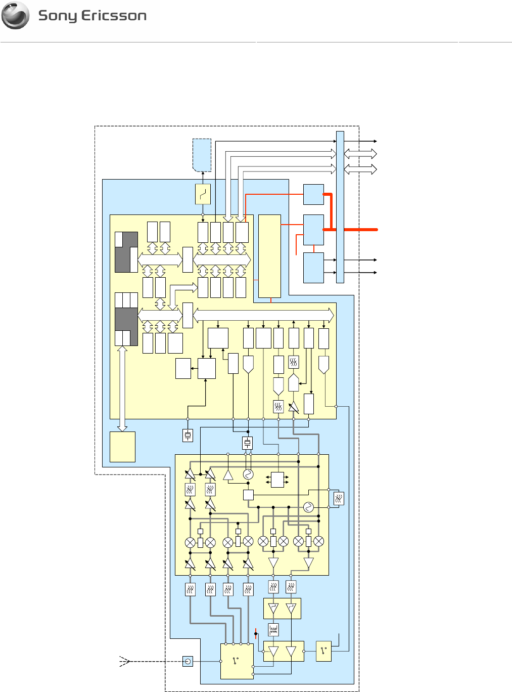
2.2 Functional Block Diagram
A function representation of the EDGE duaghter card is included in the figure below.
CACHE
Arbiter
DMA
Bridge
JTAG
Interrupt
Control
Boot
ROM
Shared
Memory
External
Memory
Power
Mngmt
Channel
Coding
Bridge
XRAM
DROM
YRAM
PROM
PRAM
ARM926EJTeakLite
DSP
Interrupt
Control
A5
Encrypt
Equalizer
Viterbi
Accel
Power
Control
TX/RX
State
Machine
GSM
Timer
RF
Serial
Port
Burst
Buffer
AGC
Register
AGC
DAC
32kHz
XTAL
13MHz
VCXO
PROCESSOR BUS
90° :4
:4
:2
PLL
Burst
Buffer
Serial
Contr
AFC
Register
PLL
PGA
D-S
ADC
Mod
MOD
DAC
AFC
DAC
90°
90°
90° :2
PA
DAC
PA
RAM
SIM
USB
GPIO
MEMORY
VOLTAGE REGULATORS
SWITCHING
REGULATOR
OV &
SCCT
PROTECTION
VOLT
REG
SYSTEM CONNECTOR
POWER USB LED
VPA
SIM INTERFACE
LEVEL
SHIFTER
POWER STATUS
LOOP FILTER
RX SAW
FILTERS
bias
PA limiter
BALUN
PMB2259
DC+ DRIVER
SWITCH
MAX4695
fixed VAPC
RFMD
RF3145
VPA
ANT SWITCH
muRata
LMSP54JA-238
INTEL
RD38F2030W0Z BASEBAND ASIC
RF TRANSCEIVER ASIC
BROADCOM BCM2132
INFINEON PMB6258
ANTENNA
CONNECTOR
EDGE MODULE
DAUGHTER CARD
UART
UART
CACHE
Arbiter
DMA
Bridge
JTAG
Interrupt
Control
Boot
ROM
Shared
Memory
External
Memory
Power
Mngmt
Channel
Coding
Bridge
XRAM
DROM
YRAM
PROM
PRAM
ARM926EJTeakLite
DSP
Interrupt
Control
A5
Encrypt
Equalizer
Viterbi
Accel
Power
Control
TX/RX
State
Machine
GSM
Timer
RF
Serial
Port
Burst
Buffer
AGC
Register
AGC
DAC
32kHz
XTAL
13MHz
VCXO
PROCESSOR BUS
90° :4
:4
:2
PLL
Burst
Buffer
Serial
Contr
AFC
Register
PLL
PGA
D-S
ADC
D-S
ADC
Mod
MOD
DAC
MOD
DAC
AFC
DAC
AFC
DAC
90°
90°
90° :2
PA
DAC
PA
DAC
PA
RAM
SIM
USB
GPIO
MEMORY
VOLTAGE REGULATORS
SWITCHING
REGULATOR
OV &
SCCT
PROTECTION
VOLT
REG
SYSTEM CONNECTOR
POWER USB LED
VPA
SIM INTERFACE
LEVEL
SHIFTER
POWER STATUS
LOOP FILTER
RX SAW
FILTERS
bias
PA limiter
BALUN
PMB2259
DC+ DRIVER
SWITCH
MAX4695
fixed VAPC
RFMD
RF3145
VPA
ANT SWITCH
muRata
LMSP54JA-238
INTEL
RD38F2030W0Z BASEBAND ASIC
RF TRANSCEIVER ASIC
BROADCOM BCM2132
INFINEON PMB6258
ANTENNA
CONNECTOR
EDGE MODULE
DAUGHTER CARD
UART
UART
Figure 2-3 EDGE Daughter Card Functional Block Diagram

Confidential
USERS MANUAL
9(31)
Document number Revision
1/198 17-5/FCP 101 3317 Uen A
2.3 Features
The EDGE modem performs a set of telecom services (TS) according to GSM standard
phase 2+, ETSI and ITU-T. The functions of the modem are implemented by issuing AT
commands over a serial interface.
2.3.1 Mobile Station Characteristics
The EDGE modem can be configured for single, dual, triple and quad band GSM
functionality. The quad band characteristics of the EDGE modem are shown in the
following table.
Confidential
USERS MANUAL
10(31)
Document number Revision
1/198 17-5/FCP 101 3317 Uen A
EDGE MODEM GSM8
50 E-GSM900 GSM1800 GSM1900
Frequency range (MHz)
TX:
824-
849
RX:
869-
894
TX: 880-915
RX: 925-960
TX: 1710-1785
RX: 1805-1880
TX: 1850-1910
RX: 1930-1990
Channel spacing 200kHz
Number of channels
123 x 8
(TDMA
)
173 x 8 (TDMA) 373 x 8 (TDMA) 298 x 8 (TDMA)
Duplex spacing 45MHz 95MHz 80MHz
GSM/G
PRS GMSK
Modulation
EDGE 8-PSK
Nom. TBD Tx phase
accuracy
(burst) Max. <5° rms phase error ; <20° max peak phase error
100KH
z <+0.5dB
200KH
z <-30dB
250KH
z <-33dB
Tx Spectrum
Due to
Modulation
400KH
z <-60dB
100KH
z <-23dBm
200KH
z <-26dBm
250KH
z <-32dBm
Tx Spectrum
Due to
Switching
Transients
400KH
z <-36dBm
Receiver sensitivity
(ANT pin)
<-
102dB
m
<-102dBm <-102dBm <-102dBm
Class Class 4 Class 1
GS
M Nom. +33dBm +30dBm
Class Class E2 Class E2
Transm
itter
output
power
(ANT
conn)
ED
GE Nom. +27dBm +26dBm
Nom.
<-
104d
Bm
Receiver
sensitivity
(ANT
connector)
Max.
<-
102d
Bm

Confidential
USERS MANUAL
11(31)
Document number Revision
1/198 17-5/FCP 101 3317 Uen A
f1 -49dBm
Rx
Intermodulati
on
F0 = 2f1-f2;
|f2–f1| =
800KHz
f2 -49dBm
GPRS operation Class 10
Note that the number of frequency bands available will be dependant upon the factory
configuration. The available bands will be determined by customer requirements.

Confidential
USERS MANUAL
12(31)
Document number Revision
1/198 17-5/FCP 101 3317 Uen A
2.3.2 Environmental Conditions
The DC will support the following environmental conditions
Temperature Range (Full GSM Specification)1 -10oC to +55oC
Temperature Range (Operational) 2 -20oC to +65oC
Storage Temperature Range -20°C to +75°C
Table 2.3-1 Environmental Conditions
Notes
1. Full compliance to Type Approval and Regulatory Approval requirements between these
temperature ranges
2. Design Verification Testing (DVT) and Operational compliance between these temperature
ranges.
2.4 SIM Card
An external SIM card with 3V or 1.8V technology, can be connected to the modem via the
SIM interface pins.
2.5 Other Features
The EDGE modem supports a number of additional features including
• 07.10 multiplexing (normal mode)
• SIM application tool kit
2.6 Precautions
The EDGE modem device is ESD protected up to 4K V contact and 8K V air discharge. It
is recommended that integrators follow electronic device handling precautions when
working with any electronic device system to ensure no damage occurs to the host or the
radio device.
The EDGE modem is integrated on to the daughter card. When the card is mounted in
the host it is the responsibility of the integrator to ensure that static discharge protection
beyond the voltages specified above are designed in to the host product. If exposed, the
antenna is a vulnerable contact point for ESD.

Confidential
USERS MANUAL
13(31)
Document number Revision
1/198 17-5/FCP 101 3317 Uen A
Part 2 : Daughter Card Description
Confidential
USERS MANUAL
14(31)
Document number Revision
1/198 17-5/FCP 101 3317 Uen A
3 Mechanical Description
3.1 Physical Detail
Dimensional details given here are for reference only. For mechanical design data,
please refer to the mechanical outline drawing 151 88 - KRD 104 1025/2.
WIRELESS
MODEM
CIRCUIT
(SHIELDED) SYSTEM CONNECTOR
RF CONNECTOR
WIRELESS
MODEM
CIRCUIT
(SHIELDED) SYSTEM CONNECTOR
RF CONNECTOR
Figure 3-1 Layout Detail (reference only)
Confidential
USERS MANUAL
15(31)
Document number Revision
1/198 17-5/FCP 101 3317 Uen A
Figure 3-2 EDGE Daughter Card Primary Side View
Figure 3-3 EDGE Daughter Card Underneath View
Confidential
USERS MANUAL
16(31)
Document number Revision
1/198 17-5/FCP 101 3317 Uen A
4 System Interface
4.1 Overview
4.1.1 System Connector
All of the systems interface signals flow through a single connector; power, ground, data,
cotrol, status and GPIO.
Electrical connections to the modem are made through a 24 pin low insertion force (LIF)
vertical SMT mount FFC or FPC cable receptor. The connector is a single sided contact
type, for example the AVX Elco part 04-6244-024-011-800.
Connector type NON-ZIF (LIF) ST SMT
Contact Single
Profile Height (mm) 4.10
Number of Contacts 24
Current Rating 0.4A Max.
Voltage Rating 50V Max.
Dielectric withstanding voltage 200Vrms
Contact Material Phosphor bronze Tin-Plated
Insulator material Heat resistant plastic
Operating temperature 40ºC~+85ºC
FFC/FPC thickness 0.3±0.05
Table 4.1-1 Connector Characteristics
DATUM MARK
(DATUM PIN)
DETAIL A
PIN 1
PIN 24
DETAIL A
0.2 ±0.05
0.5 TYP
11.5
12.6
DATUM MARK
(DATUM PIN)
DETAIL A
PIN 1
PIN 24
DETAIL A
0.2 ±0.05
0.5 TYP
11.5
12.6
Figure 4-1 Connector Detail
Confidential
USERS MANUAL
17(31)
Document number Revision
1/198 17-5/FCP 101 3317 Uen A
Pin Name Function
1 USB_DN USB differential (-) line
2 USB_DP USB differential (+) line
3 VREF Modem logic voltage reference output from daughter card
4 OVP Over voltage protection output from daughter card
5 SPARE
6 SPARE
7 SPARE
8 GND Ground
9 GND Ground
10 GND Ground
11 GND Ground
12 GND Ground
13 GND Ground
14 VIN Voltage input from host application
15 VIN Voltage input from host application
16 VIN Voltage input from host application
17 VIN Voltage input from host application
18 VIN Voltage input from host application
19 VIN Voltage input from host application
20 RI Ring Indicator output from daughter card
21 3V3 Application reference voltage input to daughter card
22 LED Pulsing LED output from daughter card
23 UVP Under voltage & short circuit protection output from daughter card
24 P_EN Power ON enable input to daughter card
Table 4.1-2 Pin List

Confidential
USERS MANUAL
18(31)
Document number Revision
1/198 17-5/FCP 101 3317 Uen A
4.2 Electrical Interface Detail Format
Details of each electrical interface is contained in paragraph 5 (beginning page 19). The
description of each interface follows a common format. An example is shown below:
Interface Name
This is the name of the interface; usually this is the actual name found in the pin list;
sometimes this is a collective name for a number of signals, such as the example
shown here for a UART.
Function:
This identifies the basic function of the interface; some interfaces are grouped
according to their functional sub-class.
Description:
The description contains a basic overview of the interface and its functional
relationship with the host.
Pin Numbers:
All pin numbers associated with the interface are listed; these will not necessarily
be in numerical order but may be arranged to coincide with signal name list.
Signal Names:
All sigal names associated with the interface exactly as shown in the pin list; the
signal names also contain information on signal flow direction.
If not used:
This gives specific details, for each signal, of how to terminate the physical
connection if it is not required by the host; failure to observe this convention may
result in unstable operation of the EDGE modem. (This may not be necessary in the
host application since all signals have a defined function).

Confidential
USERS MANUAL
19(31)
Document number Revision
1/198 17-5/FCP 101 3317 Uen A
5 Electrical Interface
This section describes each signal line of the electrical interface between the EDGE
modem and the host equipment application. A summary of the function of each signal is
provided, together with any additional relevant information.
Signals are described from the perspective of the EDGE modem and Daughter Card
circuitry. Consequently signals described as input are inputs to the modem, driven by the
host [host⇒modem]. Likewise, signals described as output are driven by the modem in to
the host [modem⇒host]. Bi-directional signal flow (I/O) is indicated by a double-headed
arrow [modem⇔host]. In some instances the [daughter card] will be identified if the
modem circuitry is not directly involved, or where additional interface circuitry resides
between the host and the modem.
Signals which are pulled internally are identified in parentheses beside the signal name as
either (PU)=Pulled Up or (PD)=Pulled Down. Signals with no designation are not pulled
either way.
5.1 Power Interfaces
This section describes the power, ground, and other signals that control or indicate power
states.
• VIN
• 3V3
• VREF
• GND
5.1.1 VIN
Function: Daughter card power supply
Description: Primary voltage supply to switching regulator (5.5 to 20.0V).
Pin Numbers: 14, 15, 16, 17, 18, 19
Signal Names: VIN [host⇒daughter card]
If not used: Required
Details:
Power provided by the host will range from 5.5V minimum to a maximum 20.0V,
dependent upon the battery discharge state. The Daughter Card has on board regulation
which regulates the supply range to a steady 3.6V by means of a switching regulator rated
at 3A max.

Confidential
USERS MANUAL
20(31)
Document number Revision
1/198 17-5/FCP 101 3317 Uen A
Typical Electrical Characteristics:
Parameter Condition Low Mid High Unit
Voltage 5.5 7.4 20.0 V
Peak* GSM850
2-slot TX
1880 1500 950 est
Transmit mode
Power Consumption
(worst case) average GSM850
2-slot TX
450 340 145 est
mA
Idle mode
Power Consumption
(worst case)
average DRX 2 9.9 7.6 3.8 est mA
*Peak current consumption is an instantaneous value which occurs during a TDMA
transmitter burst.
Table 5.1-1: VIN Electrical Characteristics
Confidential
USERS MANUAL
21(31)
Document number Revision
1/198 17-5/FCP 101 3317 Uen A
5.1.2 3V3
Function: Daughter card reference voltage
Description: Host reference to protection circuit & USB (3.3V)
Pin Numbers: 21
Signal Names: 3V3 [host⇒daughter card]
If not used: Required
Details:
The host supplies a 3.3V regulated supply to the Daughter Card for two primary functions:
• reference supply for the undervoltage / short circuit protection circuitry
• input for the USB interface
Electrical Characteristics:
Parameter Condition Min Nom Max Unit
Voltage 3.30 V
Ripple 100 mV
5.1.3 VREF
Function: Voltage Reference
Description: Core digital voltage reference from modem.
Pin Number: 3
Signal Name: VREF [modem⇒host]
If not used: Required
Details:
VREF is supplied as a reference voltage from the modem. This reference is the modem’s
core digital supply voltage at a nominal 2.80V.
The interface is capable of sourcing 200uA and is intended primarily for situations where
host interface circuitry is required to be level shifted to maintain wireless modem signal
level compatibility. If more current is required by the host, a current amplifier must be
implemented.
Confidential
USERS MANUAL
22(31)
Document number Revision
1/198 17-5/FCP 101 3317 Uen A
This signal can also be used to indicate whether the wireless modem is powered on or
not. A high level (2.7V to 2.9V) indicates that the modem is powered on. A low level
(<0.5V) indicates that the modem is powered off.
All digital logic, except the SIM interface, is characteristic CMOS logic operating at VREF.
Electrical Characteristics:
Parameter Condition Min Typ Max Unit
inactive 0.3 0.5 V
VREF output voltage active 2.70 2.80 2.90 V
VREF output current IOUT 200 uA
Table 5.1-2: VREF Electrical Characteristics
5.1.4 GND
Function: Ground
Description: Modem common rail
Pin Numbers: 8, 9, 10, 11, 12, 13
Signal Name: GND
If not used: Required
Details:
Return path for all currents.
Confidential
USERS MANUAL
23(31)
Document number Revision
1/198 17-5/FCP 101 3317 Uen A
5.2 Status Interfaces
Status interfaces indicate or control status features of the modem.
• UVP
• OVP
• RI
• LED
• VREF
5.2.1 UVP
Function: Under voltage protection
Description: Status indicator to host of potential malfunction in Daughter Card
circuitry
Pin Number: 23
Signal Name: UVP (PD) [daughter card⇒host]
If not used: Required
Details:
The Daughter Card has FET circuitry which uses 3V3 as a reference, driving an output to
the host indicating the voltage condition of the of VBAT (the modem supply voltage). A
resistive divider connected to VBATT presents a very low Vbe to the UVP transistor. This
presents a steady state low voltage output under normal VBAT conditions with external
pulldown circuitry. In the event of a short circuit or high current fault condition on the
Daughter Card, the voltage drop from the switching regulator will bias the UVP transistor
on and present a high output to the host equipment monitoring circuit.
The UVP signal should be pulled low by the application circuit for correct function.
Electrical Characteristics:
Parameter Condition Min Typ Max Unit
Normal 0.5 V
UVP output voltage Fault 3.3 V
Table 5.2-1: UVP Electrical Characteristics
Confidential
USERS MANUAL
24(31)
Document number Revision
1/198 17-5/FCP 101 3317 Uen A
5.2.2 OVP
Function: Over voltage protection
Description: Status indicator to host of potential malfunction in Daughter Card
circuitry
Pin Number: 4
Signal Name: OVP (PU) [daughter card⇒host]
If not used: Required
Details:
The OVP signal is simply an output from the main onboard regulator. In it’s operational
state under normal functional conditions this will output 3.6V nominal
Parameter Condition Min Typ Max Unit
Normal 3.6 V
UVP output voltage Fault 3.7 V
Table 5.2-2: OVP Electrical Characteristics
5.2.3 RI
Function: Ring Indicator
Description: Alert signal from the modem to indicate an incoming SMS, or
unmasked unsolicited response
Pin Number: 20
Signal Name: RI [modem⇒host]
If not used: Leave open
Details:
Ring Indicator is essentially a wake-up call from the modem to the host application to
signal one of two events:
• an in-coming message (SMS).
• an unmasked unsolicited response/result code.
For the EDGE modem the Ring Indicator is implemented as a GPIO interface within the
EDGE baseband device.

Confidential
USERS MANUAL
25(31)
Document number Revision
1/198 17-5/FCP 101 3317 Uen A
A falling edge indicates an alert or message. The signal remains low for a period of time
before going high. An SMS-page or unsolicited response/result code generates one pulse
(the length is configurable using an AT command)[TBC].
The ring indicator is implemented on the daughter card as an open collector transistor
output to allow the host the convenience of driving the host equipment circuitry.
5.2.4 LED
Function: LED
Description: LED-signal indicating a status change
Pin Number: 22
Signal Name: LED [modem⇒host]
If not used: Leave open
Details:
The LED is implemented on the Daughter Card as an open collector transistor output
which providesa driver level interface to an LED acting as a status indicator for the user.
The LED output can be made to blink at a rate pre-determined by modem software.
5.2.5 VREF
The function of VREF is already described in 5.1.3. This interface can be used as a
status indicator to the host that the modem is still powered. VREF is present whilst the
modem is powered and is removed upon the completion of the modem power down. This
feature can be useful in the event of a communications lock-up between the host and the
daughter card.

Confidential
USERS MANUAL
26(31)
Document number Revision
1/198 17-5/FCP 101 3317 Uen A
5.3 Data Communication and Control Interfaces
The serial data and control interfaces consist of the following :
• USB
• P_EN
5.3.1 USB Interface
Function: USB data communication port
Description: USB transmit and receive port for data communication between
modem and host.
Pin Numbers: 1, 2
Signal Names: USB_DP (2) [modem⇔host]
USB_DN (1) [modem⇔host]
If not used: Required
Details:
Power to the USB interface is provided by the 3V3 input from the host.
5.3.2 P_EN
Function: Power Enable
Description: Modem power enable control from host
Pin Numbers: 24
Signal Names: P_EN [host⇒daughter card]
If not used: Required
Details:
The power enable signal is provided from the host application and is routed to the
switching regulator shutdown input and also to the REG_EN (regulator enable) pin on the
modem. Assertion of this pin will initiate power up. The P_EN pin is active high and has
to be maintained continually in order to keep the modem powered.

Confidential
USERS MANUAL
27(31)
Document number Revision
1/198 17-5/FCP 101 3317 Uen A
5.4 ANTENNA CONNECTOR
Function: Antenna connector
Description: 50 ohm wireless antenna connection.
Pin Numbers: N/A
Signal Names: ANTENNA
If not used: Required
Details:
The antenna interface to the modem is routed to a low profile coaxial connector on the
daughter card. The antenna connector has a nominal impedance of 50 ohms and a
maximum frequency rating of 2.5GHz.
IMPORTANT NOTE:
FCC Radiation Exposure Statement:
This equipment complies with FCC radiation exposure limits set forth for an uncontrolled
environment. This equipment should be installed and operated with minimum distance of
20cm between the radiator and your body.
This transmitter must not be co-located or operating in conjunction with any other antenna
or transmitter.
Confidential
USERS MANUAL
28(31)
Document number Revision
1/198 17-5/FCP 101 3317 Uen A
6 Rudimentary Circuit Functions
This section contains some rudimentary circuit functions for the sequencing of powering
the modem up and down.
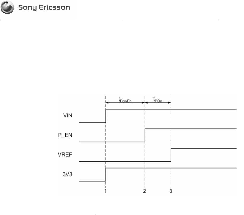
6.1 Power On Sequence
This sequence illustrates the power on procedure.
Figure 6-1 Power On Sequence
Sequence Detail:
1 VIN and 3V3 are supplied to the modem by the host. These two voltages can be
supplied simultaneously when the Daughter Card is required to be powered on.
Both voltages must be present before the power on sequence is initiated for the
Daughter Card to function correctly.
2 Once VIN and 3V3 voltages are applied the host can enable power up by
asserting power enable signal P_EN. The power up process will begin.
3 VREF may be used as an indicator that the modems regulators are powered.
tPOn is typically less than 70 ms
Confidential
USERS MANUAL
29(31)
Document number Revision
1/198 17-5/FCP 101 3317 Uen A
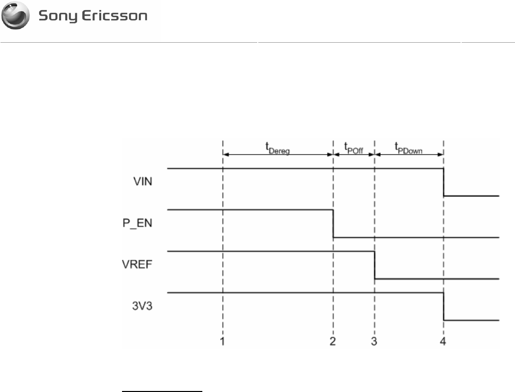
6.2 Power Off Sequence
This sequence illustrates the power off procedure.
Figure 6-2 Power Off Sequence
Sequence Detail:
1 The “AT+CFUN=4” instruction is sent from the host application to the modem in
order to initiate a deregistration sequence.
2 The modem responds to the request with an ‘OK’ to indicate that deregistration
is completed. Deregistration from the network can take from 3-30 seconds.
After de-registration has been acknowledged the host application may remove
P_EN.
3 The switching regulator output capacitor will gradually discharge until the modem
regulators threshold is exceeded. and power down will be complete. VREF may
be used as indicator of complete shut down.
4 When the modem has successful shutdown, and VREF has fallen bellow 0.5V
then the host may safely remove VIN and 3V3 at any time. However the
supplies can remain active without increasing current consumption (typically
<25uA).
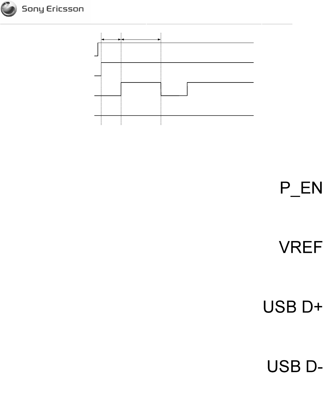
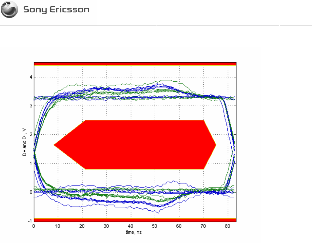
6.3 USB communications timing
This sequence illustrates USB initialization.
Confidential
USERS MANUAL
30(31)
Document number Revision
1/198 17-5/FCP 101 3317 Uen A
1. The startup sequence begins with the completion of the power up ramping of the
VREF signal as described in Power On Sequence.
2. The D+ signal is brought high with the power up of the USB block in the
baseband circuitry. This produces the J state indicating to the USB host that a
device is attaching.
3. A host initiated SE0 begins the USB protocol transactions. A power up
summary of USB transactions is shown for example.
Transactions by Device:
#Transactns Acknowledgement Bytes
Addr Endp Type Total Error ACK NAK None Attempt Success
0 0 SETUP 4 0 4 0 0 32 32
0 0 IN 4 0 4 0 0 36 36
0 0 OUT 2 0 2 0 0 0 0
3 0 SETUP 7 0 7 0 0 56 56
3 0 IN 7 0 7 0 0 132 132
3 0 OUT 6 0 6 0 0 0 0
4 0 SETUP 3 0 3 0 0 24 24
4 0 IN 3 0 3 0 0 27 27
4 0 OUT 2 0 2 0 0 0 0
4 2 IN 7164 0 3 7161 0 63 63
4 2 OUT 2 0 2 0 0 39 39
Control Transfers by Device:
Addr Endp Packet# Dir Type Recipient Request Value Index Length
0 0 336 D->H Standard Device GET_DESCRIPTOR 256 0 64
0 0 426 H->D Standard Device SET_ADDRESS 3 0 0
0 0 874 D->H Standard Device GET_DESCRIPTOR 256 0 64
0 0 904 H->D Standard Device SET_ADDRESS 4 0 0
3 0 472 D->H Standard Device GET_DESCRIPTOR 256 0 18
3 0 481 D->H Standard Device GET_DESCRIPTOR 512 0 9
3 0 490 D->H Standard Device GET_DESCRIPTOR 512 0 255
3 0 670 D->H Standard Device GET_DESCRIPTOR 256 0 18
3 0 679 D->H Standard Device GET_DESCRIPTOR 512 0 9
3 0 688 D->H Standard Device GET_DESCRIPTOR 512 0 39
3 0 697 H->D Standard Device SET_CONFIGURATION 1 0 0
4 0 950 D->H Standard Device GET_DESCRIPTOR 256 0 18
4 0 959 D->H Standard Device GET_DESCRIPTOR 512 0 9
4 0 968 H->D Standard Device SET_CONFIGURATION 1 0 0
Confidential
USERS MANUAL
31(31)
Document number Revision
1/198 17-5/FCP 101 3317 Uen A
Eye Diagram for Full Speed USB signaling.