Southern Avionics SD100 Non Directional Radiobeacon (NDB) User Manual fcc short
Southern Avionics Company Non Directional Radiobeacon (NDB) fcc short
SD100 Manual

Box 5345 • Beaumont • Texas • 77726-5345 • USA • Phone (409) 842-1717 • Fax (409) 842-2987
www.southernavionics.com
SD SERIES TRANSMITTER
MANUAL # SD410002
REVISION: A
DRAFT
Printed
May 27, 2004
Box 5345 • Beaumont • Texas • 77726-5345 • USA • Phone (409) 842-1717 • Fax (409) 842-2987
www.southernavionics.com
SOUTHERN AVIONICS COMPANY
MANUFACTURERS OF LOW FREQUENCY RADIOBEACONS AND ASSOCIATED PRODUCTS
5000 BELMONT, P.O. BOX 5345 / BEAUMONT, TEXAS 77726-5345 USA
TELEPHONE: (409) 842-1717; FAX: (409) 842-2987; CABLE: SAC; TELEX; 77-9450
ONE YEAR LIMITED WARRANTY
SOUTHERN AVIONICS COMPANY (hereinafter called COMPANY) warrants to the original purchaser for a period of
one year from the date of delivery to the original purchaser, that the goods sold pursuant to this COMPANY invoice
were at the time of the delivery, free from defects resulting from faulty material or workmanship. THIS LIMITED
WARRANTY IS IN LIEU OF ALL OTHER REPRESENTATIONS AND EXPRESS WARRANTIES. This warranty is
made for the benefit of the initial purchaser only and is not made for the benefit of any party other than initial purchaser.
It applies only if the goods are submitted to normal use and service and does not apply if the goods are
misused or mismatched with other goods such as antennas, couplers, or any other third party goods that
have not been approved by SAC in writing for use with SAC equipment.
ALL IMPLIED WARRANTIES EXISTING UNDER THE LAW ARE HEREBY EXPRESSLY NEGATED;
PARTICULARLY, COMPANY HEREBY NEGATES AND DISCLAIMS THE IMPLIED WARRANTY OF
MERCHANTABILITY AND IMPLIED WARRANTY OF FITNESS FOR A PARTICULAR PURPOSE.
If Purchaser believes that these goods do not comply with the express warranty stated above or any existing and
applicable implied warranty which under the law cannot be disclaimed or negated as provided above, then purchaser
may request the COMPANY inspect such goods by mailing, within sixty (60) days after purchaser knows or should
have known that the goods allegedly do not conform with the warranty, postage prepaid, to COMPANY, P.O. Box 5345,
5000 Belmont, Beaumont, Texas, 77726 Attention: President, a writing specifying (a) purchaser's name, address, and
telephone number, (b) date of purchase, (c) COMPANY distributor or location from which the goods were purchased,
(d) location of the goods in question (or include the goods in question with the notice), and (e) brief description of the
alleged nonconformity with the warranty. If the goods are covered by, and do not conform with, the warranty,
COMPANY will repair or replace F.O.B. point of manufacture any such goods; but in no event will COMPANY be
obligated or required to remove the non-conforming goods from their place of installation or to install the replacement
goods. All replacement goods are warranted to the extent provided herein for the remaining term of this warranty.
In the event purchaser chooses to commence an action for breach of warranty or breach of contract arising out of the
sale of the goods pursuant to this invoice, the purchaser must commence such action within one year after the course
of action accrues.
THE REMEDY PROVIDED HEREIN SHALL BE THE SOLE AND EXCLUSIVE REMEDY FOR BREACH OF THIS
WARRANTY, FOR ANY BREACH OF ANY IMPLIED WARRANTY EXISTING AND APPLICABLE UNDER THE LAW
(TO THE EXTENT THAT ANY SUCH WARRANTY HAS NOT BEEN SUCCESSFULLY NEGATED AND DISCLAIMED
HEREINABOVE), AND FOR ANY ACT OF NEGLIGENCE OR ANY OTHER TORTIOUS ACT COMMITTED BY
COMPANY, AND IN NO EVENT SHALL THE COMPANY BE LIABLE TO PURCHASER OR ANY THIRD PARTY FOR
ANY INCIDENTAL, CONSEQUENTIAL OR SPECIAL DAMAGES RESULTING FROM ANY DEFECT IN THE GOODS
OR ANY FAILURE OF THE GOODS TO CONFORM WITH THIS WARRANTY OR ANY IMPLIED WARRANTY
EXISTING AND APPLICABLE UNDER THE LAW (TO THE EXTENT THAT ANY SUCH IMPLIED WARRANTY HAS
NOT BEEN SUCCESSFULLY NEGATED AND DISCLAIMED HEREINABOVE.)

Box 5345 • Beaumont • Texas • 77726-5345 • USA • Phone (409) 842-1717 • Fax (409) 842-2987
www.southernavionics.com
REPAIR POLICY
Repair Rate: One Hundred Twenty ($120) Dollars per hour plus Parts.
Minimum Repair Cost: One Hundred Twenty ($120) Dollars.
Maximum Repair Cost: Seventy-five (75) percent of the price for a new or reconditioned item or its direct
replacement. If an item sent to SAC for Repair is determined to be non-repairable and is replaced by a
new or reconditioned item, the Customer is not charged for any costs incurred in time and materials spent
in efforts to repair that particular non-repairable item. The Customer will only be charged the price of the
replacement item. All non-repairable items are returned to the Customer. However if the Customer does
not purchase a new or reconditioned item to replace that particular non-repairable item the Minimum
Repair Cost is applied.
Turnaround Time: Southern Avionics Company’s standard Turnaround Time is 45 days. Customers that
request the Repair be processed in less than 45 days will be charged an Expediting Fee of Thirty ($30)
Dollars per hour in addition to the standard Repair Rate.
RMA (Return Material Authorization): Southern Avionics Company requires all items submitted to our
factory for Repair must be accompanied by a Return Merchandise Authorization (RMA) Number. Please
make a RMA request before returning items to Southern Avionics Company. This is the best way to
communicate with us and ensure that your needs are taken care of. A RMA Number may be obtained by
contacting
Angela Flores, Sales Administrator
either by telephone at 409-842-1717, extension 111 or by
e-mail at angelaf@southernavionics.com .
Rejection: Southern Avionics Company reserves the right to refuse repair of any items that SAC deems
to be non-repairable to our factory standards. Pads lifted from circuit boards or burnt circuit boards are
examples of grounds for rejection.
Freight Costs: The Customer pays for freight costs to and from Southern Avionics Company. SAC will not
be responsible for any loss or damage of any items in transit either to or from SAC.
Expiration of Support: SAC supports all items manufactured by SAC for no less than ten (10) years from
date of original purchase. SAC will not repair any items that are older than ten (10) years old. Any items
sent to SAC for repair that are more than ten (10) years old will be returned to the sender freight collect to
the return address provided unless otherwise specified in writing prior to the receipt of the returned item by
SAC.
Box 5345 • Beaumont • Texas • 77726-5345 • USA • Phone (409) 842-1717 • Fax (409) 842-2987
www.southernavionics.com
Serial Numbers: Southern Avionics Company will not repair any items that are not accompanied by the
Serial Numbers of the finished goods associated with the items.
Estimates: SAC will not provide any estimates of costs other than the costs outlined above.
Warranty: Repairs are guaranteed for 90 days after shipment. Warranty applies only to Repairs made
and does not cover subsequent equipment failures not associated with the previous Repair.

SD SERIES TRANSMITTER
i
•
•
•
•
•
•
SOUTHERN AVIONICS COMPANY
TABLE OF CONTENTS
1 INTRODUCTION: . . . . . . . . . . . . . . . . . . . . . . . . . . . . . . . . . . . . . . . . . . . . . . . . . . . . . . . . . . 1
1.2 SPECIFICATIONS: SD Series Dual . . . . . . . . . . . . . . . . . . . . . . . . . . . . . . . . . . . . . . 2
General Description: SD25 . . . . . . . . . . . . . . . . . . . . . . . . . . . . . . . . . . . . . . . . . . . . . . . . . 2
General Description: SD50 . . . . . . . . . . . . . . . . . . . . . . . . . . . . . . . . . . . . . . . . . . . . . . . . . 5
General Description: SD100 . . . . . . . . . . . . . . . . . . . . . . . . . . . . . . . . . . . . . . . . . . . . . . . . 8
2 THEORY OF OPERATION, SD SERIES UNIT . . . . . . . . . . . . . . . . . . . . . . . . . . . . . . . . . 15
2.1 Functional Description: SD Series Transmitter . . . . . . . . . . . . . . . . . . . . . . . . . . . . . . 15
2.2 SLF31002/00 - Basic Dual Transmitter . . . . . . . . . . . . . . . . . . . . . . . . . . . . . . . . . . . 30
2.2.1 P.A. PCB . . . . . . . . . . . . . . . . . . . . . . . . . . . . . . . . . . . . . . . . . . . . . . . . . . . . . . . . . 30
SLP10001 - Assemlby, PCB, RF Power Amplifier . . . . . . . . . . . . . . . . . . . . . . . . . . . . . 31
2.2.2 RF PA Power Supply PCB . . . . . . . . . . . . . . . . . . . . . . . . . . . . . . . . . . . . . . . . . . . 34
SLP10003 -Assembly, PCB, RF PA Power Supply . . . . . . . . . . . . . . . . . . . . . . . . . . . . . 36
2.2.3 Analog I/O and Audio PCB . . . . . . . . . . . . . . . . . . . . . . . . . . . . . . . . . . . . . . . . . . . 41
SLP10005 - Assembly, Analog I/O and Audio . . . . . . . . . . . . . . . . . . . . . . . . . . . . . . . . . 42
2.2.4 Controller / Monitor PCB . . . . . . . . . . . . . . . . . . . . . . . . . . . . . . . . . . . . . . . . . . . . 47
SLP10007 - Assembly, PCB, Controller / Monitor . . . . . . . . . . . . . . . . . . . . . . . . . . . . . . 50
2.2.4 Digital I/O and PWM PCB . . . . . . . . . . . . . . . . . . . . . . . . . . . . . . . . . . . . . . . . . . . 54
SLP10009 - Assembly, PCB, Digital I/O and PWM . . . . . . . . . . . . . . . . . . . . . . . . . . . . . 55
2.3 Detailed Circuit Analysis: Dual Transmitter . . . . . . . . . . . . . . . . . . . . . . . . . . . . . . . . 57
2.3.1 SLP10012 - Controller Motherboard . . . . . . . . . . . . . . . . . . . . . . . . . . . . . . . . . . . . 57
2.3.2 Dual Low Voltage Power Supply PCB . . . . . . . . . . . . . . . . . . . . . . . . . . . . . . . . . . . 60
SLP10017 - Assembly, Low voltage Power Supply (Coldfire) . . . . . . . . . . . . . . . . . . . . . 61
2.4 SLE10004 - Load Center . . . . . . . . . . . . . . . . . . . . . . . . . . . . . . . . . . . . . . . . . . . . . . . 65
2.4.1 User Interface PCB . . . . . . . . . . . . . . . . . . . . . . . . . . . . . . . . . . . . . . . . . . . . . . . . . . 66
SLP10006 - Assembly, PCB, User Interface . . . . . . . . . . . . . . . . . . . . . . . . . . . . . . . . . . . 67
2.5 SLM10005 - Control Monitor Panel . . . . . . . . . . . . . . . . . . . . . . . . . . . . . . . . . . . . . . 70
2.5.1 Local Control PCB . . . . . . . . . . . . . . . . . . . . . . . . . . . . . . . . . . . . . . . . . . . . . . . . . . 71
2.5.2 Audio PCB . . . . . . . . . . . . . . . . . . . . . . . . . . . . . . . . . . . . . . . . . . . . . . . . . . . . . . . . 77
2.5.1 Filter/Bridge PCB . . . . . . . . . . . . . . . . . . . . . . . . . . . . . . . . . . . . . . . . . . . . . . . . . . . 78
SLP10002/01 - Assembly, PCB Filter/Bridge (Standard Band) . . . . . . . . . . . . . . . . . . . . 79
3 INSTALLATION AND OPERATION . . . . . . . . . . . . . . . . . . . . . . . . . . . . . . . . . . . . . . . . . 81
4 MAINTENANCE . . . . . . . . . . . . . . . . . . . . . . . . . . . . . . . . . . . . . . . . . . . . . . . . . . . . . . . . . 101
4.1 ALIGNMENT AND ADJUSTMENT . . . . . . . . . . . . . . . . . . . . . . . . . . . . . . . . . . . . 101
4.2 CONTROL MONITOR . . . . . . . . . . . . . . . . . . . . . . . . . . . . . . . . . . . . . . . . . . . . . . . 101
4.2.1 ANALOG I/O ALIGNMENT . . . . . . . . . . . . . . . . . . . . . . . . . . . . . . . . . . . . . . . . 101
4.2.2 DIGITAL I/O ALIGNMENT . . . . . . . . . . . . . . . . . . . . . . . . . . . . . . . . . . . . . . . . . 103
4.2.3 AUDIO OPTION (AWOS) ALIGNMENT . . . . . . . . . . . . . . . . . . . . . . . . . . . . . . 104
4.3 TRANSMITTER . . . . . . . . . . . . . . . . . . . . . . . . . . . . . . . . . . . . . . . . . . . . . . . . . . . . 106
4.3.1 PA POWER SUPPLY ALIGNMENT (PAPS) . . . . . . . . . . . . . . . . . . . . . . . . . . . 106
4.3.2 RF POWER AMPLIFIER ALIGNMENT (PA) . . . . . . . . . . . . . . . . . . . . . . . . . . . 109
4.3.3 FILTER / BRIDGE ALIGNMENT (FB) . . . . . . . . . . . . . . . . . . . . . . . . . . . . . . . . 112
5 ANTENNAS: . . . . . . . . . . . . . . . . . . . . . . . . . . . . . . . . . . . . . . . . . . . . . . . . . . . . . . . . . . . . 115
5.1 Mast Antenna . . . . . . . . . . . . . . . . . . . . . . . . . . . . . . . . . . . . . . . . . . . . . . . . . . . . . . . 115
5.2 "H" Antenna . . . . . . . . . . . . . . . . . . . . . . . . . . . . . . . . . . . . . . . . . . . . . . . . . . . . . . . . 116
5.3 50-Foot Guyed Mast Antenna . . . . . . . . . . . . . . . . . . . . . . . . . . . . . . . . . . . . . . . . . . 116
5.4 Symmetrical "T" Antenna . . . . . . . . . . . . . . . . . . . . . . . . . . . . . . . . . . . . . . . . . . . . . 116

SD SERIES TRANSMITTER
ii
•
•
•
•
•
•
SOUTHERN AVIONICS COMPANY
TABLE OF CONTENTS
6 PARTS LISTS . . . . . . . . . . . . . . . . . . . . . . . . . . . . . . . . . . . . . . . . . . . . . . . . . . . . . . . . . . . 118
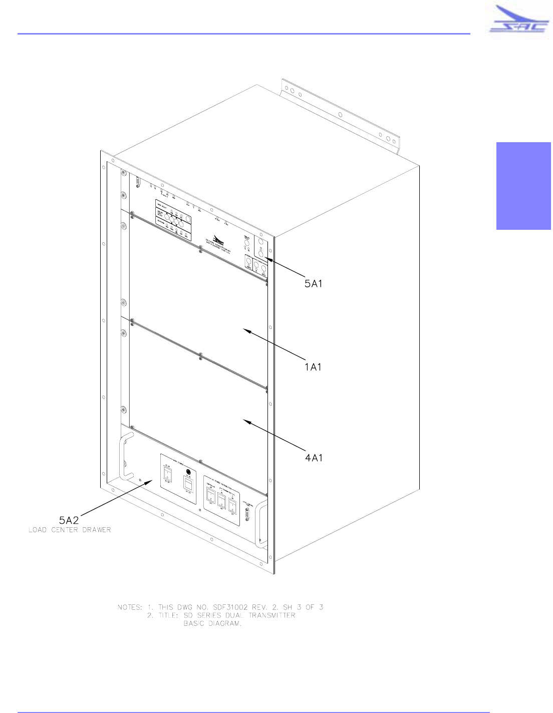
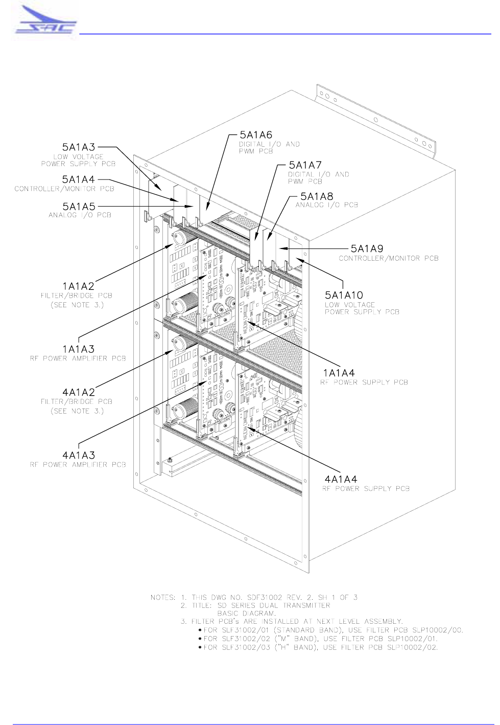
SLF31002/00 - ASSY, TRANSMITTER, SD SERIES DUAL (BASIC) . . . . . . . . . . . . 118
SLE10004 - ASSY, LOAD CENTER (SD SERIES) . . . . . . . . . . . . . . . . . . . . . . . . . . . 119
SLE10031 - ASSY, FINAL TRANSMITTER DUAL (SD SERIES) . . . . . . . . . . . . . . . 120
SLM10001 - ASSY, TRANSMITTER ENCLOSURE (SD SERIES) . . . . . . . . . . . . . . 121
SLM10005 - ASSY, CONTROL MONITOR PANEL WITH APPLIQUE . . . . . . . . . . 122

SD SERIES TRANSMITTER
iii
•
•
•
•
•
•
SOUTHERN AVIONICS COMPANY
TABLE OF FIGURES
SDE10018 - DUAL TRANSMITTER PORTRAIT. . . . . . . . . . . . . . . . . . . . . . . . . . . . . . . . . . . 11
SDE10018 - DUAL TRANSMITTER PORTRAIT WITH LOCAL CONTROL PANEL . . . . . 12
SDE10018 - TRANSMITTER ENCLOSURE DIMENSIONS . . . . . . . . . . . . . . . . . . . . . . . . . . 13
SDB10001 - SD SERIES SINGLE TRANSMITTER BLOCK DIAGRAM. . . . . . . . . . . . . . . . 23
SDB10002 - SD SERIES DUAL TRANSMITTER BLOCK DIAGRAM . . . . . . . . . . . . . . . . . 24
SDF31002 - SD SERIES BASIC DUAL TRANSMITTER DIAGRAM . . . . . . . . . . . . . . . . . . 25
SDF31002 - SD SERIES BASIC DUAL TRANSMITTER DIAGRAM - CONTINUED . . . . . 26
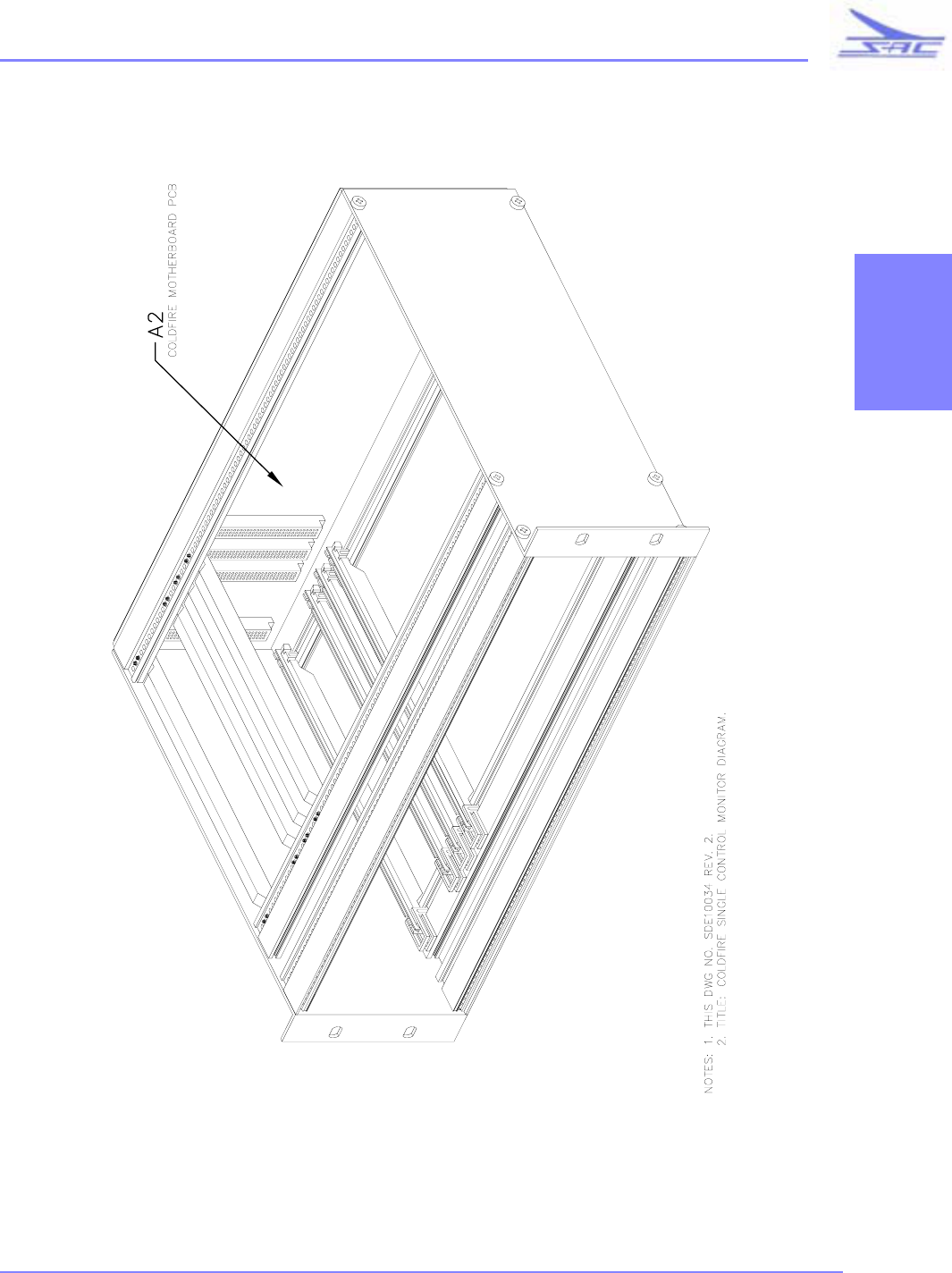
SDE10034 - SINGLE CONTROL DIAGRAM . . . . . . . . . . . . . . . . . . . . . . . . . . . . . . . . . . . . . . 27
SDE10032 - DUAL CONTROL 3U DIAGRAM. . . . . . . . . . . . . . . . . . . . . . . . . . . . . . . . . . . . . 28
SDE10033 - DUAL TRANSMITTER CONTROL 6U DIAGRAM . . . . . . . . . . . . . . . . . . . . . . 29
SDE10004 - SD SERIES LOAD CENTER DRAWER DIAGRAM. . . . . . . . . . . . . . . . . . . . . . 65
SDM10005 - LOCAL CONTROL PANEL DIAGRAM . . . . . . . . . . . . . . . . . . . . . . . . . . . . . . . 70
649 - DIAGRAM, ANTENNA REACTANCE . . . . . . . . . . . . . . . . . . . . . . . . . . . . . . . . . . . . . 117

SD SERIES TRANSMITTER
SECTION 1
1
•
•
•
•
•
•
SOUTHERN AVIONICS COMPANY
1 INTRODUCTION:
SD Series Introduction
The SD Series model beacon transmitters are computer controlled systems designed around the Motorola
ColdFire® microprocessor. These systems are capable of remote monitoring and maintenance via several
communication methods including RS232, RS 422, and RS485 protocols. An optional operator front panel offers the
common user controls normally found on an analog transmitter. These panels may also be used for remote control.
With the exception of main power application, all aspects of transmitter setup and operation come under the direct
control of the Controller / Monitor. The following are all programmable:
* Direct Digital Synthesis (DDS) of RF frequency and Audio Tone Frequency
* Identifier Morse code dot, dash and space intervals.
* Customer IDENT sequence
* Standard Alarms
* Additional Fault handling based on multipoint voltage, current and temperature monitoring
* Transfer Criteria (Dual Only)
* Power limits
* Modulation limits
The Controller / Monitor itself can be controlled and monitored by another computer system connected locally via
one of the hard wire protocols mentioned above or remotely using phone lines or any other carrier which can handle a
standard US Robotics modem spectral output.
SDSeries General Theory of Operation

SD SERIES TRANSMITTER
2
•
•
•
•
•
•
SOUTHERN AVIONICS COMPANY
1.2 SPECIFICATIONS: SD Series Dual
General Description: SD25
This non-directional beacon is an Amplitude Modulated transmitter with an adjustable output power from 5 to 25
watts. The transmitter uses switching technology in the power amplifiers and modulator / regulator modules resulting
in a highly efficient system, in a small package.
The exciter portion consists of an embedded 32-bit micro controller, an I/O interface circuit, an A/D converter, a
monitor circuitry, and an optional voice processing circuitry in a single 3U enclosure. The controller has one "stored"
non-volatile memory, redundant RF DDS (Direct Digital Synthesizer), redundant AF (Tone) DDS, and two serial
ports (local and remote). Settings for ID mode, ID code, ID rate, sequence of operation and other parameters are set
by an user interface program. Simple controls such as power adjustment, percent modulation, and side transfer are
available locally for technical setup. Also for convenience, PA voltage, PA current, PA temperature, RF frequency,
Tone frequency, Carrier power and percent modulation are displayed locally via 7-segment readouts. A simple switch
disables remote control operation during local technical service.
The power portion of each transmitter consists of two independent 25 watts systems. Each system has an output filter,
a switching power amplifier and switching modulator / regulator, power supply, and an optional battery supply.
The SD25 Dual consists of two independent SD25 transmitters and a Digitally Controlled Automatic Transfer unit
housed in a single cabinet designed for outdoor use.
Transmitter: Model SD25
Qualifications: Meets applicable requirements of ICAO, FCC, FAA, Transport Canada, UK CAA, EC (emissions
and safety standards).
Frequency Range: 190-1800 kHz, selectable in 500 Hz increments, stability better than .005% (-40(C to +70(C).
Power Output: Digitally generated carrier power into 50 ohms continuously adjustable 5 to 25 watts.
Spurious Emission: Radiated harmonics (measured at a dummy antenna) are more than 63 dB below the 25-watt
carrier.
Type of Emission: NON, A2A, A3E (Optional), GID (with optional GPS beacon modulator), or any combination.
Modulation: Digital generated typically 400 or 1020 Hz.
Noise and Hum Level: More than 40 dB below the carrier level.
Input Power: 115/230V (15%, single phase 50-60 Hz. 24 VDC.
Efficiency: Better than 70% overall efficiency AC input to RF output at 25-watt carrier and tone keying at 95%
modulation.
Numeric Digital Display Meters: Power output, reflected power, PA voltage, PA current, percent modulation, audio
input level.
Keyer: Any combination of Morse code letters or numerals with any user set values pertaining to the length of dots
and dashes, the time between them and the number of repetitions of the identification code per minute (character
length dependent).
Circuit Protection: Open and short circuit proof and immune to damage that can be cause by improper antenna
loads. Individual fuses are used to protect the AC and DC circuits and immune to severe damage caused by improper
installation. VSWR circuit that shuts down the transmitter if VSWR exceeds an adjustable value. Over temperature
and standby shutdown.

SD SERIES TRANSMITTER
SECTION 1
3
•
•
•
•
•
•
SOUTHERN AVIONICS COMPANY
Working Conditions: Continuous unattended operation in the following environments: ambient temperature, -40(C
to +70(C; relative humidity, 0-100%; high salinity as encountered in offshore conditions. IP66. Cooling by heat
sinks with no fans.
Monitoring: Transmitter shuts down with loss of tone, drop in modulation below an adjustable value, or continuous
tone, or when power falls below an adjustable value, or when VSWR rises above an adjustable value or when
temperature rises above an adjustable value or in the event of a change in the code, its duration or rate. With a dual
system, a shutdown signal initiates a transfer from the primary transmitter to the secondary transmitter.
Self-Diagnostics: Computer diagnostic routines that identify malfunctioning modules at LRU level available via
local or remote PC. Transmitter and antenna coupler are suitable for installation and operation by untrained
personnel.
Automatic Transfer Unit
Local Radiobeacon Control Panel (can be operated independently from the RMM or dial up RMM and takes
priority over both when used)
ANALOG CONTROL FUNCTIONS:
TRANSMITTER ON/OFF
PRIMARY TRANSMITTER SELECT
RESET TO PRIMARY
NORMAL/TEST
REMOTE PANEL DISABLE
DIAL UP CONTROL DISABLE
AUDIBLE ALARM ENABLE/DISABLE
POWER
ANALOG INDICATORS:
TRANSMITTER ON
PRIMARY TRANSMITTER (TRANSMITTER 1/TRANSMITTER 2)
SYSTEM STATUS
PRIMARY: Selected PRIMARY transmitter operating
SECONDARY: Selected PRIMARY transmitter failed and SECONDARY transmitter operating
FAIL: Both transmitters failed
AUDIBLE ALARM (Alarms whenever system status is FAIL).
REMOTE PANEL DISABLED
DIAL UP CONTROL DISABLED
Remote Radiobeacon Control Panel (Operates independently from the dial up RMM and has priority when
used)
ANALOG CONTROL FUNCTIONS:
TRANSMITTER ON/OFF
PRIMARY TRANSMITTER SELECT
RESET TO PRIMARY
AUDIBLE ALARM ENABLE/DISABLE
POWER
ANALOG INDICATORS:
TRANSMITTER ON
AC POWER present (at transmitter site),
PRIMARY TRANSMITTER (TRANSMITTER 1/TRANSMITTER 2)
SYSTEM STATUS

SD SERIES TRANSMITTER
4
•
•
•
•
•
•
SOUTHERN AVIONICS COMPANY
PRIMARY: Selected PRIMARY transmitter operating
SECONDARY: Selected PRIMARY transmitter failed and SECONDARY transmitter operating
FAIL: Both transmitters failed
AUDIBLE ALARM (Alarms whenever system status is FAIL).
DIAL UP CONTROL DISABLED
POWER: 115/230 VAC ±20% 50/60 Hz 5VA.
CIRCUIT PROTECTION: AC line fuse. Control link is transformer isolated by signal transformer meeting MIL-
T-27D specifications and 1000 V RMS insulation test voltage. Logic line inputs are isolated by series impedances
and diode clamps.
WORKING CONDITIONS: Continuous unattended operation in the following environment: ambient temperature
-50°C to 70°C, relative humidity 0 to 100% without condensing moisture.
INSTALLATION REQUIREMENTS: The REMOTE RADIOBEACON CONTROL PANEL is designed for
indoor mounting in a standard 19-inch cabinet. Panel height is 7 inches; required panel depth is 5 inches.

SD SERIES TRANSMITTER
SECTION 1
5
•
•
•
•
•
•
SOUTHERN AVIONICS COMPANY
General Description: SD50
This non-directional beacon is an Amplitude Modulated transmitter with an adjustable output power from 5 to 50
watts. The transmitter uses switching technology in the power amplifiers and modulator / regulator modules resulting
in a highly efficient system, in a small package.
The exciter portion consists of an embedded 32-bit micro controller, an I/O interface circuit, an A/D converter, a
monitor circuitry, and an optional voice processing circuitry in a single 3U enclosure. The controller has one "stored"
non-volatile memory, redundant RF DDS (Direct Digital Synthesizer), redundant AF (Tone) DDS, and two serial
ports (local and remote). Settings for ID mode, ID code, ID rate, sequence of operation and other parameters are set
by an user interface program. Simple controls such as power adjustment, percent modulation, and side transfer are
available locally for technical setup. Also for convenience, PA voltage, PA current, PA temperature, RF frequency,
Tone frequency, Carrier power and percent modulation are displayed locally via 7-segment readouts. A simple switch
disables remote control operation during local technical service.
The power portion of each transmitter consists of two independent 50 watts systems. Each system has an output filter,
a switching power amplifier and switching modulator / regulator, power supply, and an optional battery supply.
The SD50 Dual consists of two independent SD50 transmitters and a Digitally Controlled Automatic Transfer unit
housed in a single cabinet designed for outdoor use.
Transmitter: Model SD50
Qualifications: Meets applicable requirements of ICAO, FCC, FAA, Transport Canada, UK CAA, EC (emissions
and safety standards).
Frequency Range: 190-1800 kHz, selectable in 500 Hz increments, stability better than .005% (-40(C to +70(C).
Power Output: Digitally generated carrier power into 50 ohms continuously adjustable 5 to 25 watts.
Spurious Emission: Radiated harmonics (measured at a dummy antenna) are more than 63 dB below the 50-watt
carrier.
Type of Emission: NON, A2A, A3E (Optional), GID (with optional GPS beacon modulator), or any combination.
Modulation: Digital generated typically 400 or 1020 Hz.
Noise and Hum Level: More than 40 dB below the carrier level.
Input Power: 115/230V (15%, single phase 50-60 Hz. 24 VDC.
Efficiency: Better than 70% overall efficiency AC input to RF output at 50-watt carrier and tone keying at 95%
modulation.
Numeric Digital Display Meters: Power output, reflected power, PA voltage, PA current, percent modulation, audio
input level.
Keyer: Any combination of Morse code letters or numerals with any user set values pertaining to the length of dots
and dashes, the time between them and the number of repetitions of the identification code per minute (character
length dependent).
Circuit Protection: Open and short circuit proof and immune to damage that can be cause by improper antenna
loads. Individual fuses are used to protect the AC and DC circuits and immune to severe damage caused by improper
installation. VSWR circuit that shuts down the transmitter if VSWR exceeds an adjustable value. Over temperature
and standby shutdown.
Working Conditions: Continuous unattended operation in the following environments: ambient temperature, -40(C
to +70(C; relative humidity, 0-100%; high salinity as encountered in offshore conditions. IP66. Cooling by heat
sinks with no fans.

SD SERIES TRANSMITTER
6
•
•
•
•
•
•
SOUTHERN AVIONICS COMPANY
Monitoring: Transmitter shuts down with loss of tone, drop in modulation below an adjustable value, or continuous
tone, or when power falls below an adjustable value, or when VSWR rises above an adjustable value or when
temperature rises above an adjustable value or in the event of a change in the code, its duration or rate. With a dual
system, a shutdown signal initiates a transfer from the primary transmitter to the secondary transmitter.
Self-Diagnostics: Computer diagnostic routines that identify malfunctioning modules at LRU level available via
local or remote PC. Transmitter and antenna coupler are suitable for installation and operation by untrained
personnel.
Automatic Transfer Unit
Local Radiobeacon Control Panel (can be operated independently from the RMM or dial up RMM and takes
priority over both when used)
ANALOG CONTROL FUNCTIONS:
TRANSMITTER ON/OFF
PRIMARY TRANSMITTER SELECT
RESET TO PRIMARY
NORMAL/TEST
REMOTE PANEL DISABLE
DIAL UP CONTROL DISABLE
AUDIBLE ALARM ENABLE/DISABLE
POWER
ANALOG INDICATORS:
TRANSMITTER ON
PRIMARY TRANSMITTER (TRANSMITTER 1/TRANSMITTER 2)
SYSTEM STATUS
PRIMARY: Selected PRIMARY transmitter operating
SECONDARY: Selected PRIMARY transmitter failed and SECONDARY transmitter operating
FAIL: Both transmitters failed
AUDIBLE ALARM (Alarms whenever system status is FAIL).
REMOTE PANEL DISABLED
DIAL UP CONTROL DISABLED
Remote Radiobeacon Control Panel (Operates independently from the dial up RMM and has priority when
used)
ANALOG CONTROL FUNCTIONS:
TRANSMITTER ON/OFF
PRIMARY TRANSMITTER SELECT
RESET TO PRIMARY
AUDIBLE ALARM ENABLE/DISABLE
POWER
ANALOG INDICATORS:
TRANSMITTER ON
AC POWER present (at transmitter site),
PRIMARY TRANSMITTER (TRANSMITTER 1/TRANSMITTER 2)
SYSTEM STATUS
PRIMARY: Selected PRIMARY transmitter operating
SECONDARY: Selected PRIMARY transmitter failed and SECONDARY transmitter operating
FAIL: Both transmitters failed

SD SERIES TRANSMITTER
SECTION 1
7
•
•
•
•
•
•
SOUTHERN AVIONICS COMPANY
AUDIBLE ALARM (Alarms whenever system status is FAIL).
DIAL UP CONTROL DISABLED
POWER: 115/230 VAC ±20% 50/60 Hz 5VA.
CIRCUIT PROTECTION: AC line fuse. Control link is transformer isolated by signal transformer meeting MIL-
T-27D specifications and 1000 V RMS insulation test voltage. Logic line inputs are isolated by series impedances
and diode clamps.
WORKING CONDITIONS: Continuous unattended operation in the following environment: ambient temperature
-50°C to 70°C, relative humidity 0 to 100% without condensing moisture.
INSTALLATION REQUIREMENTS: The REMOTE RADIOBEACON CONTROL PANEL is designed for
indoor mounting in a standard 19-inch cabinet. Panel height is 7 inches; required panel depth is 5 inches.

SD SERIES TRANSMITTER
8
•
•
•
•
•
•
SOUTHERN AVIONICS COMPANY
General Description: SD100
This non-directional beacon is an Amplitude Modulated transmitter with an adjustable output power from 5 to 100
watts. The transmitter uses switching technology in the power amplifiers and modulator / regulator modules resulting
in a highly efficient system, in a small package.
The exciter portion consists of an embedded 32-bit micro controller, an I/O interface circuit, an A/D converter, a
monitor circuitry, and an optional voice processing circuitry in a single 3U enclosure. The controller has one "stored"
non-volatile memory, redundant RF DDS (Direct Digital Synthesizer), redundant AF (Tone) DDS, and two serial
ports (local and remote). Settings for ID mode, ID code, ID rate, sequence of operation and other parameters are set
by an user interface program. Simple controls such as power adjustment, percent modulation, and side transfer are
available locally for technical setup. Also for convenience, PA voltage, PA current, PA temperature, RF frequency,
Tone frequency, Carrier power and percent modulation are displayed locally via 7-segment readouts. A simple switch
disables remote control operation during local technical service.
The power portion of each transmitter consists of two independent 100 watts systems. Each system has an output
filter, a switching power amplifier and switching modulator / regulator, power supply, and an optional battery supply.
The SD100 Dual consists of two independent SD100 transmitters and a Digitally Controlled Automatic Transfer unit
housed in a single cabinet designed for outdoor use.
Transmitter: Model SD100
Qualifications: Meets applicable requirements of ICAO, FCC, FAA, Transport Canada, UK CAA, EC (emissions
and safety standards).
Frequency Range: 190-1800 kHz, selectable in 500 Hz increments, stability better than .005% (-40(C to +70(C).
Power Output: Digitally generated carrier power into 50 ohms continuously adjustable 5 to 100 watts.
Spurious Emission: Radiated harmonics (measured at a dummy antenna) are more than 63 dB below the 100-watt
carrier.
Type of Emission: NON, A2A, A3E (Optional), GID (with optional GPS beacon modulator), or any combination.
Modulation: Digital generated typically 400 or 1020 Hz.
Noise and Hum Level: More than 40 dB below the carrier level.
Input Power: 115/230V (15%, single phase 50-60 Hz. 24 VDC.
Efficiency: Better than 70% overall efficiency AC input to RF output at 100-watt carrier and tone keying at 95%
modulation.
Numeric Digital Display Meters: Power output, reflected power, PA voltage, PA current, percent modulation, audio
input level.
Keyer: Any combination of Morse code letters or numerals with any user set values pertaining to the length of dots
and dashes, the time between them and the number of repetitions of the identification code per minute (character
length dependent).
Circuit Protection: Open and short circuit proof and immune to damage that can be cause by improper antenna
loads. Individual fuses are used to protect the AC and DC circuits and immune to severe damage caused by improper
installation. VSWR circuit that shuts down the transmitter if VSWR exceeds an adjustable value. Over temperature
and standby shutdown.
Working Conditions: Continuous unattended operation in the following environments: ambient temperature, -40(C
to +70(C; relative humidity, 0-100%; high salinity as encountered in offshore conditions. IP66. Cooling by heat
sinks with no fans.

SD SERIES TRANSMITTER
SECTION 1
9
•
•
•
•
•
•
SOUTHERN AVIONICS COMPANY
Monitoring: Transmitter shuts down with loss of tone, drop in modulation below an adjustable value, or continuous
tone, or when power falls below an adjustable value, or when VSWR rises above an adjustable value or when
temperature rises above an adjustable value or in the event of a change in the code, its duration or rate. With a dual
system, a shutdown signal initiates a transfer from the primary transmitter to the secondary transmitter.
Self-Diagnostics: Computer diagnostic routines that identify malfunctioning modules at LRU level available via
local or remote PC. Transmitter and antenna coupler are suitable for installation and operation by untrained
personnel.
Automatic Transfer Unit
Local Radiobeacon Control Panel (can be operated independently from the RMM or dial up RMM and takes
priority over both when used)
ANALOG CONTROL FUNCTIONS:
TRANSMITTER ON/OFF
PRIMARY TRANSMITTER SELECT
RESET TO PRIMARY
NORMAL/TEST
REMOTE PANEL DISABLE
DIAL UP CONTROL DISABLE
AUDIBLE ALARM ENABLE/DISABLE
POWER
ANALOG INDICATORS:
TRANSMITTER ON
PRIMARY TRANSMITTER (TRANSMITTER 1/TRANSMITTER 2)
SYSTEM STATUS
PRIMARY: Selected PRIMARY transmitter operating
SECONDARY: Selected PRIMARY transmitter failed and SECONDARY transmitter operating
FAIL: Both transmitters failed
AUDIBLE ALARM (Alarms whenever system status is FAIL).
REMOTE PANEL DISABLED
DIAL UP CONTROL DISABLED
Remote Radiobeacon Control Panel (Operates independently from the dial up RMM and has priority when
used)
ANALOG CONTROL FUNCTIONS:
TRANSMITTER ON/OFF
PRIMARY TRANSMITTER SELECT
RESET TO PRIMARY
AUDIBLE ALARM ENABLE/DISABLE
POWER
ANALOG INDICATORS:
TRANSMITTER ON
AC POWER present (at transmitter site),
PRIMARY TRANSMITTER (TRANSMITTER 1/TRANSMITTER 2)
SYSTEM STATUS
PRIMARY: Selected PRIMARY transmitter operating
SECONDARY: Selected PRIMARY transmitter failed and SECONDARY transmitter operating
FAIL: Both transmitters failed

SD SERIES TRANSMITTER
10
•
•
•
•
•
•
SOUTHERN AVIONICS COMPANY
AUDIBLE ALARM (Alarms whenever system status is FAIL).
DIAL UP CONTROL DISABLED
POWER: 115/230 VAC ±20% 50/60 Hz 5VA.
CIRCUIT PROTECTION: AC line fuse. Control link is transformer isolated by signal transformer meeting MIL-
T-27D specifications and 1000 V RMS insulation test voltage. Logic line inputs are isolated by series impedances
and diode clamps.
WORKING CONDITIONS: Continuous unattended operation in the following environment: ambient temperature
-50°C to 70°C, relative humidity 0 to 100% without condensing moisture.
INSTALLATION REQUIREMENTS: The REMOTE RADIOBEACON CONTROL PANEL is designed for
indoor mounting in a standard 19-inch cabinet. Panel height is 7 inches; required panel depth is 5 inches.
SD SERIES TRANSMITTER
SECTION 1
11
•
•
•
•
•
•
SOUTHERN AVIONICS COMPANY
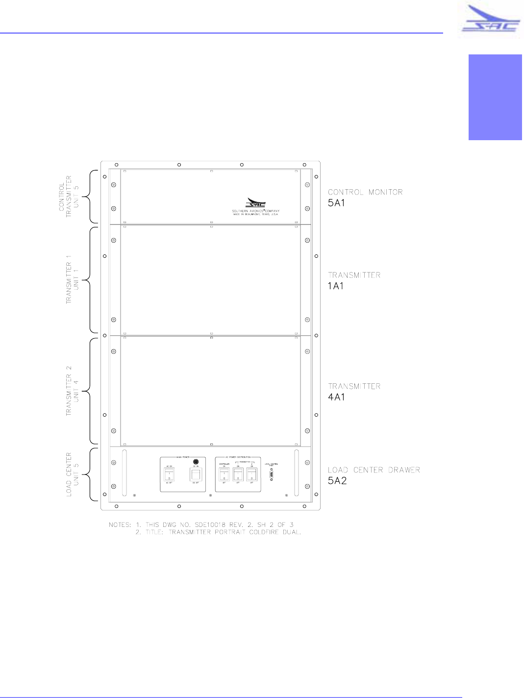
SDE10018 - DUAL TRANSMITTER PORTRAIT
SD SERIES TRANSMITTER
12
•
•
•
•
•
•
SOUTHERN AVIONICS COMPANY
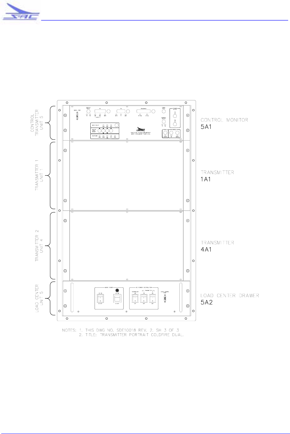
SDE10018 - DUAL TRANSMITTER PORTRAIT WITH LOCAL CONTROL PANEL
SD SERIES TRANSMITTER
SECTION 1
13
•
•
•
•
•
•
SOUTHERN AVIONICS COMPANY
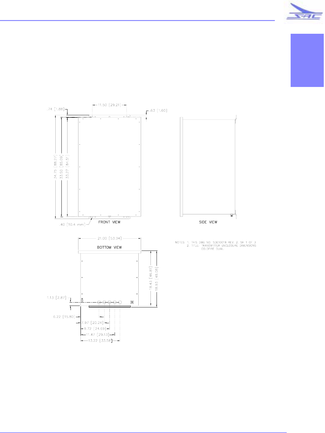
SDE10018 - TRANSMITTER ENCLOSURE DIMENSIONS

SD SERIES TRANSMITTER
14
•
•
•
•
•
•
SOUTHERN AVIONICS COMPANY
This page is intentionally left blank.

SD SERIES TRANSMITTER
15
•
•
•
•
•
•
SOUTHERN AVIONICS COMPANY
SECTION 2
2 THEORY OF OPERATION, SD SERIES UNIT
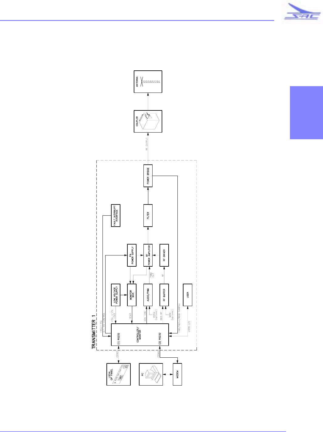
2.1 Functional Description: SD Series Transmitter
General Theory of Operation
Briefly, the SDxx system takes advantage of the powerful Motorola ColdFire(r) microprocessor. It is located on the
Controller / Monitor PCB and is the heart of the system, generally controling all system operation either directly or in
conjunction with an Analog and Digital I/O multiplexing interface.
The following are all controlled by the embedded firmware, Direct Digital Synthesis (DDS) of RF
frequency and AF tone frequency , Identifier Morse code dot, dash and space intervals., Customer IDENT sequence,
the standard alarms, any additional Fault handling based on multipoint voltage, current and temperature monitoring ,
transfer criteria (Dual Only), power limiting and modulation limiting.
RS 232,RS422 and RS485 protocols are supported. A US Robotics Modem is furnished for using phone lines.
The RF section consists of the RF PA Power Supply, The RF PA Amplifier, The Filter /Bridge, and the
Mother Board which interconnects them all. This section is interconnected with the Controller/Monitor which
Dictates the Frequency of operation, power output, and modulation percentage. Operational information is also
passed. A more detailed breakdown as to functionality follows on a board by board basis.
SLP10007 - Controller / Monitor
The CONTROLLER/ MONITOR employs the new Motorola MCF5206 COLDFIRE(r) microprocessor. It
encompasses the following sections:
COLDFIRE Processor - 32-bit
ADC - 8-Channel 12-bit
DAC - 8-Channel 8-bit
DDS - Radio Frequency (190K to 1800KHz)
DDS - Tone Frequency (400 / 1020 Hz)
Flash Memory - 4Mb
DRAM - 16Mb
Programmable Logic
Digital I/O (Read/Write)
UART
Watch Timer and NV-RAM
COLDFIRE Processor section:
The LOGIC program creates 16MHz from 32MHz for the clock frequency of the microprocessor. The processor
controls several peripheral functions such as memory, task timers, I/O bus lines, and RS-232 ports. For the dual
system, the primary Controller / Monitor and secondary Controller / Monitor may talk to each other through
Controller / Monitor Motherboard (SLP10012) by using 2 COM-PORT lines (ex: RXD & TXD). Each Controller /
Monitor has one interrupt line for paying attention what other Controller / Monitor has something is important, then
Controller / Monitor sets "RS-232" MUX to be enabled.
Analog-to-Digital converter (ADC) section:
The Controller / Monitor Controller PCB has two (AD7891) 12-bit ADC chips, so there are 16 analog inputs. The
channel selection of input range is 0 to +5 V.

SD SERIES TRANSMITTER
16
•
•
•
•
•
•
SOUTHERN AVIONICS COMPANY
Digital-to-Analog Converter (DAC) section:
The 8-bit DAC provides eight digitally controlled dc voltage outputs. The limited of output range is 0 to +5 V. The
user may adjust dc analog level or turn on/off likely digital level.
RF Direct Digital Synthesizer (DDS) section:
The 50MHz clock input is for the RF DDS. The RF DDS provides two different signal-waves (square wave and sine
wave). The square wave level is 0 to +5.0 V (recommended) and the sine wave level is 0 to 1.0 V. The DDS has 8
data digitally inputs. The code may store 4 data bytes for the 32-bit RF DDS tuning word. RF is enabled by writing
the desired frequency to the DDS, and disabled by writing a zero frequency to the DDS. The RF DDS goes the signal
through EMI filter to generate a low jitter square wave output.
Tone Frequency Direct Digital Synthesizer section:
The 50MHz clock input is also used by the AF DDS. The AF DDS signal is sine wave only. The user may adjust AF
amplitude modulation. Two methods for keying the tone are available. The first is like the RF DDS - load a frequency
into the registers of the DDS chip. The second is simply "keying" (digital ON/OFF) of a reserved I/O signal. The
settings for ID mode, ID code, ID rate, sequence of operation and other parameters are set by a user interface
program.
Flash Memory section:
Its 4Mb of memory is organized as 512K x 8. The firmware for the E(E)PROM is written in assembly / C code. It
may move data to DRAM and NV-RAM memory when the power is up. It is simple to replace when the code is
updated.
DRAM section:
The PCB has two DRAM devices. It totals 1Mb x 16 x 2 (32-bit data). During initialization the EPROM moves data
to the DRAM.
Programmable LOGIC (LATTICE device) section:
There are two LATTICE chips on the PCB. The Programmable Logic provides several necessary functions such as
control lines, 1Hz, 16MHz, enabled / disabled lines and interrupt lines.
Digital I/O section:
There are 32 digital inputs or outputs and 4 control lines for writing. Each control has 8 data lines organized as one
byte each. They are used for the status fault, frequency reading, reset, and control data.
Universal Synchronous/Asynchronous Receiver/Transmitters (UART) section:
The Controller / Monitor processor has two UARTs. They are used for RS-232 only. SAC offers four possible
transmitter configurations as follows:
Single TX without a LOCAL CONTROL panel:
The Controller / Monitor serial port 1 is probably used for PC.
The Controller / Monitor serial port 2 is used for PC / Modem through Controller / Monitor Motherboard (Controller
/ Monitor MB - SLP10012).
Single TX with a LOCAL CONTROL panel:
The Controller / Monitor serial port 1 is used for the local operating panel.
The Controller / Monitor serial port 2 is used for PC / Modem through Controller / Monitor MB.
Dual TX without a LOCAL CONTROL panel:
Either Controller / Monitor1 or Controller / Monitor2 serial port 1 is probably used for PC.
The serial port 2 is used for PC / Modem through Controller / Monitor MB.
Dual TX with a LOCAL CONTROL panel:

SD SERIES TRANSMITTER
17
•
•
•
•
•
•
SOUTHERN AVIONICS COMPANY
SECTION 2
Either Controller / Monitor1 or Controller / Monitor2 serial port 1 is used for local operating panel.
The serial port 2 is used for PC / Modem through Controller / Monitor MB.
Watch Timer and NV-RAM section:
The NV-RAM provides 32Kb of memory available to the user. The NV-RAM can hold data more than 10 years in
the absence of power. It allows the operator to store various settings in NV memory. When the power is up,
Controller / Monitor can follow the user settings in NV memory. The Watchdog timer restarts an out of control
Controller / Monitor processor. The code may use the real-time clock for 255 task timers (background).
SLP10009 Digital I/O and PWM Theory
The Digital I/O and PWM PCB consists of several sub sections which accomplish the following functions:
Digital Input State Reading
Digital Output Control
Frequency Counting
Audio to PWM Conversion
AWOS Option.
The Digital Input Section receives and conditions state information from the various system modules mainly
indicating the fault status of these sections but also monitoring the state of other sensors. While retaining their unique
state value all of these signals are combined into one interrupt request (IRQ) line for rapid servicing of external
events. A local red fault LED indicates the arrival of a fault condition. The processor take action depending on the
nature of the condition.
The Digital Output Section conditions and outputs a state condition to the various system modules primarily to
perform fault resets. Antenna switching is also controlled by this section.
The Frequency Counter section conditions and samples the Direct Digital Synthesizer generated frequency from the
RF power amplifier. This data is relayed to the processor which monitors the output RF frequency for accuracy.
The PWM section of this board inputs audio signals from the tone generating Direct Digital Synthesizer and from an
optional voice input piggybacked PCB for AWOS functionality. The composite audio signal is summed with an
adjustable DC level and converted into a 75 kHz Pulse Width Modulated signal with its basic no-audio duty cycle
being set at a fixed percentage. This fixed level facilitates modulation tracking irregardless of power level output. A
back-up modulation limiting circuit prevents over-modulation from damaging the RF Amplifier but main over
modulation protection control for Tone signals is a software function of the processor which monitors modulation at
all times.
The Optional AWOS plug in PCB Contains an AGC section which prevents over-modulation by the USER audio
signal. There is also a built in active Audio band-pass filter which eliminates signals outside of the 300 to 3000Hz
pass band. Signals generated on this Optional PCB also alert the processor which then cuts the main tone level and
temporarily ceases issuing any modulation alarms based on modulation percentage.
SLP10020 OPTIONAL AUDIO PCB (AWOS)

SD SERIES TRANSMITTER
18
•
•
•
•
•
•
SOUTHERN AVIONICS COMPANY
The Audio PCB is an OPTIONAL addition to the normal system which allows the user to broadcast AWOS
announcements. The Option is implemented as a plug in piggyback board to the Digital I/O PCB and consists of four
sections as follows:
Voice Amplifier
Automatic Gain Control
Chebychev Passband Filter
Voice Detector
The Voice amplifier takes the nominal -17dBm signal level and boost it to a level useable by the AGC
section
It is common mode balanced and its Gain is adjustable.
The AGC circuit is responsible for modulation limiting. It is adjusted to "capture" the level at -17dBm and
output a constant modulation level to the Digital I/O PWM section up to levels exceeding +10 dBm. This section
prevents inadvertent over modulation of the voice signal, and is necessary since the Controller / Monitor has no
control over user input.
The Chebychev Passband filter is designed for 300 to 3000 Hz. The output at 4000 Hz is down more than 45
dB ensuring any out of band audio signals from the USER will not cause adjacent channel interference.
The Voice Detector has two functions. It detects the presence of an announcement sequence and
automatically attenuates the Keying tone level down to 20% modulation. The announcement level is summed with
the Keying tone level and set to achieve 95% composite modulation. This action prevents over modulation and allows
the announcement to be heard over the beacon Morse code IDENT tones. It also signals the Controller /Monitor
which in turn temporarily suspends Modulation Alarms since the IDENT tone level is dropped below the alarm
threshold.
SLP10005 Analog I/O
The Analog I/O and PWM PCB consists of several sub sections which accomplish the following functions:
Analog Signal Input
Analog Signal Output
Modulation Detection
The Analog Input Section is essentially a 40 channel low pass filtered analog MUX. These multiplexed inputs are
actually an expansion scheme which adds additional analog inputs to those already available to the controller/
monitor. This allows the overall system to be expanded to control larger multi-section transmitters up to 1KW at
present.
Signals such as RF Power Amplifier voltage, current and temperature, to name only a few, are sampled and read in to
the Controller / Monitor via this MUX. The multiplexing process is directly controlled by the Controller Monitor.
The Analog Signal Output Section is a smaller MUX facilitating output control expansion. As an example,
an analog control signal originating in the Controller / Monitor such as PWR_LEVEL ( a 0.0 to 4.0 volt DC level) is

SD SERIES TRANSMITTER
19
•
•
•
•
•
•
SOUTHERN AVIONICS COMPANY
SECTION 2
sent to this Sample and Hold MUX channel 1. Via this channel the MUX outputs this particular level to the PA Power
Supply which dictates the output power level of the transmitter. The Next Channel of the MUX can control yet
another module requiring some level of control voltage if needed.
The Modulation Detector receives a detected sample of the RF envelope form the bridge circuit and converts
it into two DC levels called Vmax and Vgref. The Controller / Monitor reads in these levels and subtracts Vgref from
Vmax to derive Vmin. Vmax and Vmin are then used in the standard modulation formula to obtain modulation
percentage in the same way as someone would calculate it manually using an oscilloscope. This circuit is intended to
free the Controller / Monitor from having to sample large amounts of envelope data to statistically calculate the
percentage thereby facilitating more of a real-time monitoring of modulation. Correction curves are embedded to
resolve linearity issues arising from the detection process.
SLP10017 Low Voltage Power Supply
The LVPS Furnishes +5, +12, and -12VDC to the Controller/ Monitor Mother Board and itself plugs into the
mother PCB. It is transformer driven to allow for 115/230VAC operation. 48VDC operation allows running off of
emergency battery. The LVPS also passes 50VDC or 48V BATTERY to the user section to power miscellaneous
circuitry.
SLP10003 PA Power Supply Theory
The PA Power Supply (PAPS)
The PA Power Supply consists of three sub-sections, namely, the Inrush Current section , the DC Controller,
and the DC-DC Converter. Included with these are associated signal sense and fault circuitry. Taking them one at a
time in the general structure of their usage follows.
1.) The Inrush Current Section:
After receiving the HV-ON signal from the Controller / Monitor, this section switches on HV-DC and controls the
charge rate of the HV DC supply capacitors to avoid damagingly high inrush currents. It does this by limiting the
charge current and monitoring the voltage build-up on the large capacitor bank until it reaches an acceptable charge
level, after which unlimited current is applied. The Raw HV is sampled and fed back to the Controller / Monitor.
2.) The DC Controller
This section is a buck regulator with feedback control to reduce the Raw HV DC down to level usable by the RF
Power Amplifier section. Under Controller / Monitor control, the output of this section can be varied, which in turn
will vary the power output of the RF Power Amplifier. The feedback allows the DC Controller to respond to the peak
power demands of the PA greatly reducing or eliminating carrier droop. This section Also isolates the PA from input
power fluctuations and or "brown-outs", and maintains a steady power output over widely varying conditions. Since
the DC Controller controls the RF power output and the PA sections modulator can run a constant carrier level duty
cycle, power can be changed with out resetting the modulation percentage. The DC Controllers Voltage and Current
output is sampled and fed back to the Controller / Monitor for monitoring. Fault conditions for current and voltage
will automatically shut down the section and report to the Controller / Monitor which can attempt to bring the unit
back on line if the problem was transitory or perhaps switch transmitters if the system is a dual configuration.

SD SERIES TRANSMITTER
20
•
•
•
•
•
•
SOUTHERN AVIONICS COMPANY
3.) The DC-DC Converter
The converter will take an optional 48VDC battery back-up source and produce HV which is combined with the
normal AC HVDC to provide a seamless transition from AC to DC operation in the event of a Brownout or AC
power failure. It is purposely set lower than the nominal AC HVDC to allow for simple diode combining and to
preserve battery life while outputting a legal signal. It is NOT regulated but rather will slowly output less HV as the
batteries drain. If regulated it would draw more and more current as the batteries became weaker. Since the system is
computer controlled decisions can be made to stay on the air at reduced power levels in emergency situations
allowing battery conservation . The Converter is a basic Chopped DC-DC converter with over-current sensing and
local fault shutdown latches. The fault condition is also reported to the Controller / Monitor. A Reset of all latched
fault logic states can be is performed by the Controller / Monitor as necessary. A dual low voltage +12VDC supply
12VA and 12VB is fed by +50VDC derived from the AC line or 48VDC supplied by the battery backup ensuring
continuous operation of the low level stages after the initial power on. The separated 12V feeds ensures minimal
cross-talk between the DC-DC Controller and the DC Controller. As an aside the 50VDC supply (located elsewhere
depending on the system) is also monitored by the Controller / Monitor along with 48VDC Battery current and
voltage for diagnostic information.
SLP10001 RF Power Amplifier
The RF Power Amplifier PCB is a Pulse Width Modulator and RF power amplifier in one package. The Pulse width
Modulator section is commonly called the Modulator and the RF Power Amplifier is commonly called the PA. These
terms will be used for the rest of this discussion.
The PA section is comprised of a broadband pre-amplifier and Class "D" RF power amplifier. It inputs
either the Controller / Monitor controlled Direct Digital Synthesized RF drive signal or a customer furnished signal.
Its output power is controlled by the Modulator.
The Modulator is basically a 75 kHz buck converter. It inputs D.C. High Voltage from the PA Power supply Section
and uses a 75 kHz square-wave input from the Controller / Monitor-I/O section to chop, filter and reduce the DC-HV
to a level usable by the PA. The Voltage the Modulator outputs to the PA is a function of both the input HV and the
duty cycle of the 75 Khz square-wave. The 75 kHz Duty cycle of is set to 45% and not used to change the overall RF
Power output level. The power output level of the PA is set by changing the input DC-HV and this is done under
Controller / Monitor control. To Modulate the PA, audio frequency information in the form of a Morse Code Station
ID tone sequence or an AWOS voice announcement, pulse width modulates the 75 kHz signal controlling the
Modulator section thus varying its output voltage at the audio rate. This varies the instantaneous voltage applied to
the PA, modulating its output Power.
Critical parameters such as PA Voltage , Current , and Temperature are sensed and monitored continuously by the
Controller / Monitor. Local (on board automatic) over-current protection is built in. The protection scheme also
provides interrupt driven fault reporting to the Controller / Monitor.
SLP10002 Filter/Bridge PCB Theory
The Filter/Bridge includes a broadband toroidal impedance transformer, a seven pole Butterworth low pass
filter, a broadband RF power bridge, modulation envelope detector and associated level sampling and fault latching
circuitry.
The Impedance transformer receives as input the RF Power Amplifiers Class D output and impedance matches it to
the 50Ohm Butterworth Low Pass Filter, which is configured for optimum characteristics via simple jumpers for the
frequency band in use. The sinusoidal 50Ohm output of the Filter is Fed then fed through the RF power bridge which
reports readings of Forward and Reflected RF Power to the Controller / Monitor. The Controller / Monitor then
normalizes and calibrates the power curve and calculates SWR. Fault latches are also set up to report High reflected

SD SERIES TRANSMITTER
21
•
•
•
•
•
•
SOUTHERN AVIONICS COMPANY
SECTION 2
power or RF over-current conditions for immediate action via a fault interrupt structure. A sample of the final RF
output envelope is detected and sent back to the Controller / Monitor where other circuitry derives Vmax/Vmin
information for modulation percentage calculation via Controller / Monitor firmware.
SLP10016 - OPTIONAL Local / Remote Control
The Optional Local Control can be used as either a local or remote operating panel. The Local Control is a
microprocessor-based (Motorola M68HC11) unit offering partial control over the controller / monitor and thereby the
system. It offers similar functionality to a standard front panel on older equipment.
Pushbuttons allow the user to select and or control the following:
Primary Transmitter Select (1 or 2)
Mode Select (ID, CONT or CARR)
Transmitter Displayed (1 or 2)
And view readings of: readings for:
PA Voltage
PA Current
PA Temperature
Forward Power
Reflected Power
Modulation%
Audio Frequency (tone)
RF Frequency
The user can adjust or set the:
Modulation Percentage
RF Power output level
RF ON/OFF
Enable/Disable Alarms
Select Local/Remote Control
When one of any pushbuttons is pressed except RESET, the 6811 processor sends a data command to the Controller
/ Monitor through the serial communication port.
RESET forces Local Panel re-initialization.
The 7 segment led display update comes from the Controller / Monitor The displays provide the 3 following groups
for reading:
RF Power:
Up to 4 digits display the Modulation%, forward power and reflected power.
Power Amplifier (P.A.):
Up to 3 digits Display the voltage, current and temperature.
Frequency:
Up to 5 digits display the tone frequency (set) and RF frequency (measured).
The LED indicators simply display the system status. The Local Control receives a command string from the
Controller / Monitor and uses this to set the status indicators.

SD SERIES TRANSMITTER
22
•
•
•
•
•
•
SOUTHERN AVIONICS COMPANY
The complex logic needed to for pushbutton control and display is accomplished using programmable gate-array
logic.
The Local Control provides two serial communication ports (RS-232 / RS-485). The RS-232 port is used locally for
the Controller / Monitor serial port 1. The RS-485 port is connected remotely to the Controller / Monitor port 1.
SD SERIES TRANSMITTER
23
•
•
•
•
•
•
SOUTHERN AVIONICS COMPANY
SECTION 2
SDB10001 - SD SERIES SINGLE TRANSMITTER BLOCK DIAGRAM
SD SERIES TRANSMITTER
24
•
•
•
•
•
•
SOUTHERN AVIONICS COMPANY
SDB10002 - SD SERIES DUAL TRANSMITTER BLOCK DIAGRAM
SD SERIES TRANSMITTER
25
•
•
•
•
•
•
SOUTHERN AVIONICS COMPANY
SECTION 2
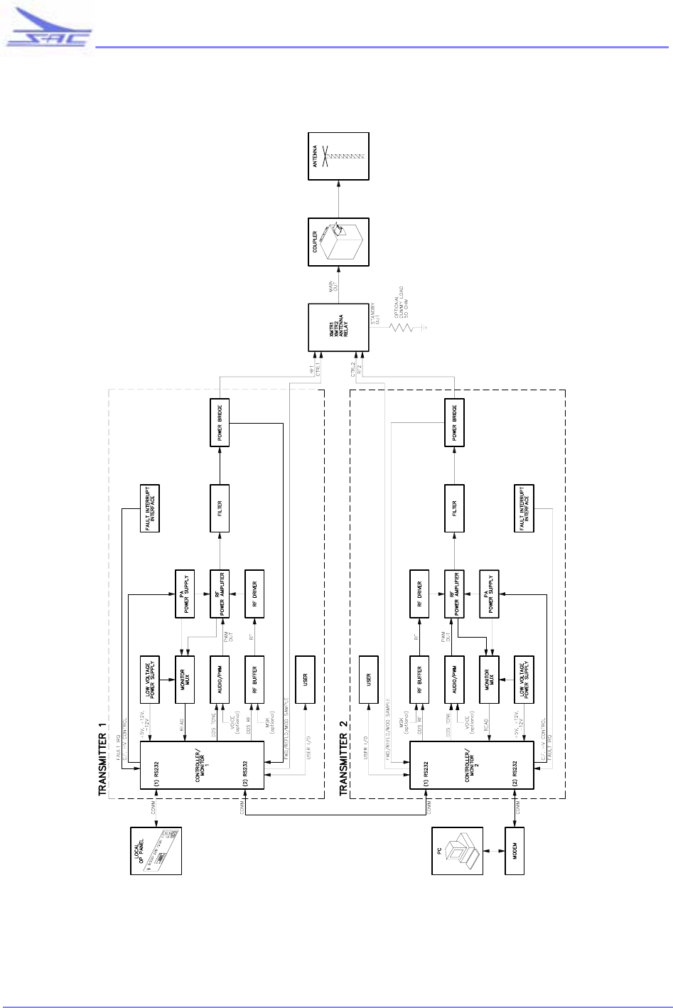
SDF31002 - SD SERIES BASIC DUAL TRANSMITTER DIAGRAM
PAGE 1 OF 2
SD SERIES TRANSMITTER
26
•
•
•
•
•
•
SOUTHERN AVIONICS COMPANY
SDF31002 - SD SERIES BASIC DUAL TRANSMITTER DIAGRAM - CONTINUED
PAGE 2 OF 2
SD SERIES TRANSMITTER
27
•
•
•
•
•
•
Southern Avionics Company
SECTION 2
SDE10034 - SINGLE CONTROL DIAGRAM
SD SERIES TRANSMITTER
28
•
•
•
•
•
•
Southern Avionics Company
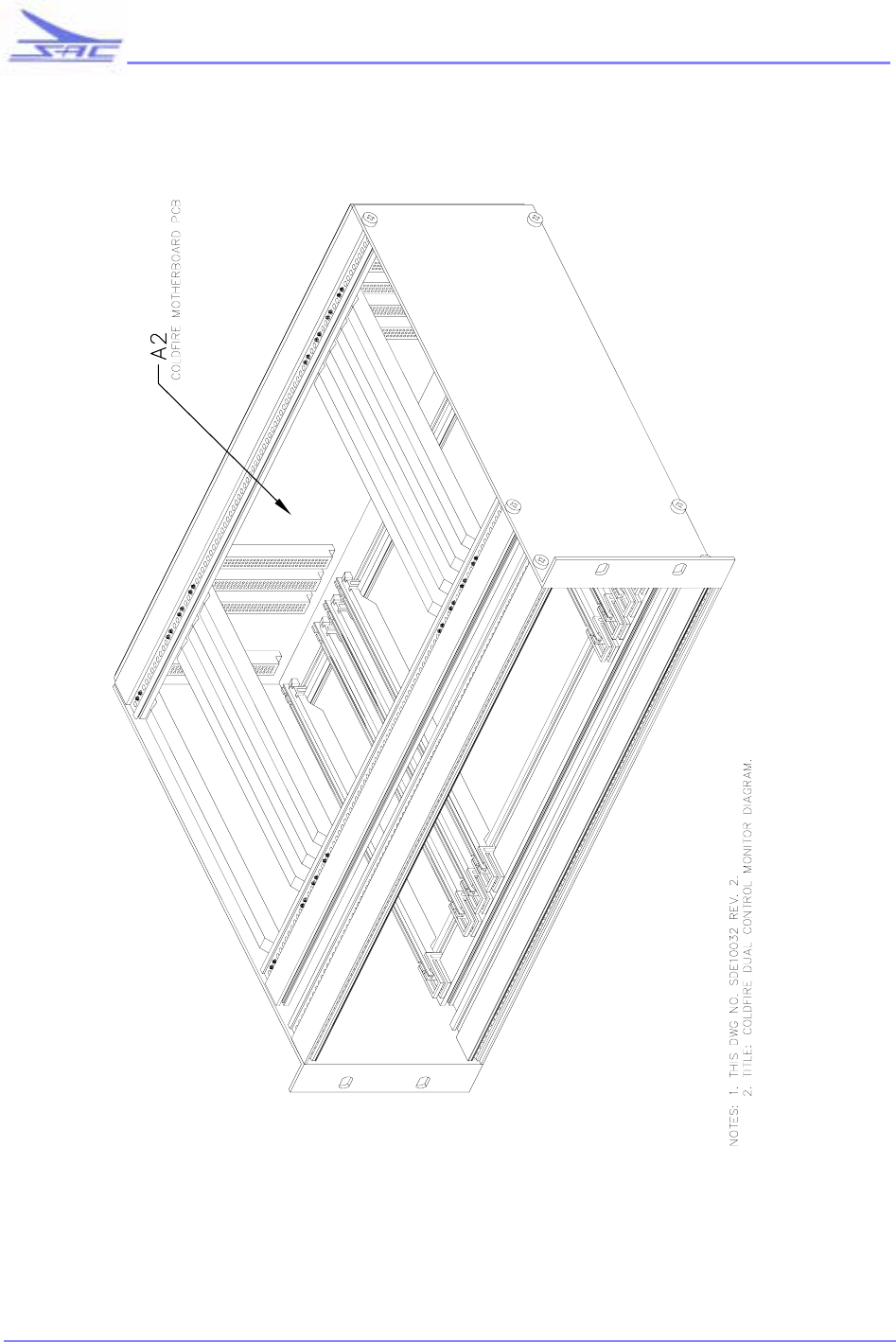
SDE10032 - DUAL CONTROL 3U DIAGRAM
SD SERIES TRANSMITTER
29
•
•
•
•
•
•
Southern Avionics Company
SECTION 2
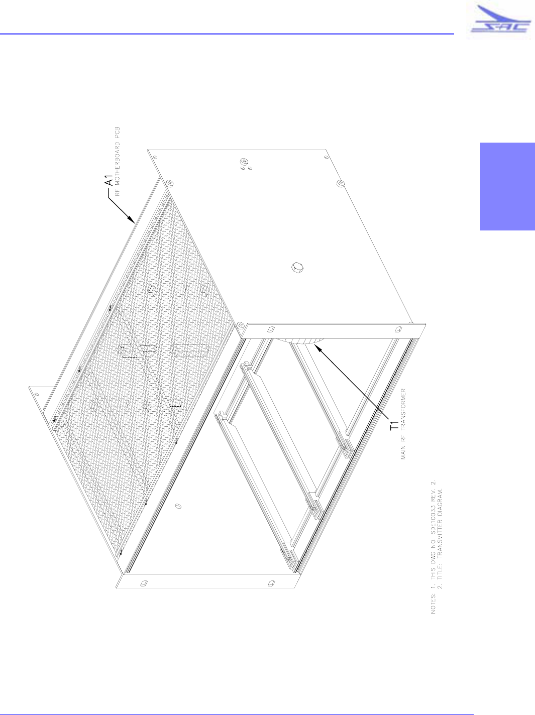
SDE10033 - DUAL TRANSMITTER CONTROL 6U DIAGRAM

SD SERIES TRANSMITTER
30
•
•
•
•
•
•
Southern Avionics Company
2.2 SLF31002/00 - Basic Dual Transmitter
2.2.1 P.A. PCB
SLP10001 RF Power Amplifier
The RF Power Amplifier PCB is a Pulse Width Modulator and RF power amplifier in one package. The Pulse width
Modulator section is commonly called the Modulator and the RF Power Amplifier is commonly called the PA.
These terms will be used for the rest of this discussion.
The PA section is comprised of a broadband pre-amplifier and Class "D" RF power amplifier. It inputs
either the Controller / Monitor controlled Direct Digital Synthesized RF drive signal or a customer furnished signal.
Its output power is controlled by the Modulator.
The Modulator is basically a 75 kHz buck converter. It inputs D.C. High Voltage from the PA Power supply
Section and uses a 75 kHz square-wave input from the Controller / Monitor-I/O section to chop, filter and reduce the
DC-HV to a level usable by the PA. The Voltage the Modulator outputs to the PA is a function of both the input HV
and the duty cycle of the 75 Khz square-wave. The 75 kHz Duty cycle of is set to 45% and not used to change the
overall RF Power output level. The power output level of the PA is set by changing the input DC-HV and this is done
under Controller / Monitor control. To Modulate the PA, audio frequency information in the form of a Morse Code
Station ID tone sequence or an AWOS voice announcement, pulse width modulates the 75 kHz signal controlling the
Modulator section thus varying its output voltage at the audio rate. This varies the instantaneous voltage applied to
the PA, modulating its output Power.
Critical parameters such as PA Voltage , Current , and Temperature are sensed and monitored continuously
by the Controller / Monitor. Local (on board automatic) over-current protection is built in. The protection scheme
also provides interrupt driven fault reporting to the Controller / Monitor.

SD SERIES TRANSMITTER
31
•
•
•
•
•
•
SOUTHERN AVIONICS COMPANY
SECTION 2
SLP10001 - Assemlby, PCB, RF Power Amplifier
REFERENCE COMPONENT DESCRIPTION
DESIGNATOR
01 SRP10001 PCB, POWER AMPLIFIER \ DMOD
C01 1C263050 CAP, 3.3M, 250V, METALLIZED FILM
C02 1C551010 CAP, CERAMIC, .1MFD. 50V, 10%
C03 1C551010 CAP, CERAMIC, .1MFD. 50V, 10%
C04 1C854750 CAP, .47 UF, 250V METAL POLY
C05 1C254750 CAP, .47M, 250V, MF
C06 1C253371 CAP, .33M 400V METALLIZED FILM
C07 1C254710 CAP, .47M 50V METAL FILM
C08 1C254710 CAP, .47M 50V METAL FILM
C09 1C851050 CAP, .1M, 250V, POLYESTER FILM
C10 1C851250 CAP, .12M, 250V, POLYESTER FILM
C11 1C551010 CAP, CERAMIC, .1MFD. 50V, 10%
C12 1C073310 CAP, 33M 50V ELCTLT
C14 1C851250 CAP, .12M, 250V, POLYESTER FILM
C15 1C073310 CAP, 33M 50V ELCTLT
C16 1C551010 CAP, CERAMIC, .1MFD. 50V, 10%
C17 1C073310 CAP, 33M 50V ELCTLT
C18 1C073310 CAP, 33M 50V ELCTLT
C19 1C561010 CAP, CERAMIC, 1MFD 50V 10%
C21 1C671000 CAP, 10 MFD, 35V, ALUMINUM ELECTROLYTIC
C22 1C551010 CAP, CERAMIC, .1MFD. 50V, 10%
C23 1C671000 CAP, 10 MFD, 35V, ALUMINUM ELECTROLYTIC
C24 1C681800 CAP, 180 MFD, 35V ALUMINUM ELECTROLYTIC
C25 1C551010 CAP, CERAMIC, .1MFD. 50V, 10%
C27 1C551010 CAP, CERAMIC, .1MFD. 50V, 10%
C28 1C551010 CAP, CERAMIC, .1MFD. 50V, 10%
C29 1C541010 CAP, CERAMIC, .01 MFD, 50V, 10%
C30 1C551010 CAP, CERAMIC, .1MFD. 50V, 10%
C31 1C561010 CAP, CERAMIC, 1MFD 50V 10%
C32 1C261020 CAP, 1M 63V FLM
C33 1C551010 CAP, CERAMIC, .1MFD. 50V, 10%
C34 1C621040 CAP, 100MF, 100V ALUMINUM ELECTROYLTIC
C35 1C631000 CAP, 1000MF, 25V ALUMINUM ELECTRYLTIC, RADIAL
C36 1C551010 CAP, CERAMIC, .1MFD. 50V, 10%
CR1 1D440000 DIODE, ULTRAFAST RECOV RCT, 600V,4A
CR2 1D440000 DIODE, ULTRAFAST RECOV RCT, 600V,4A
CR3 1D440000 DIODE, ULTRAFAST RECOV RCT, 600V,4A
CR4 1D508228 DIODE, SCHOTTKY BARRIER
CR5 1D440000 DIODE, ULTRAFAST RECOV RCT, 600V,4A
CR6 1D440000 DIODE, ULTRAFAST RECOV RCT, 600V,4A
CR7 1D620000 DIODE, TVS, 20V, BIDIRECTIONAL
CR8 1D440000 DIODE, ULTRAFAST RECOV RCT, 600V,4A
CR9 1D440000 DIODE, ULTRAFAST RECOV RCT, 600V,4A
CR10 1D620000 DIODE, TVS, 20V, BIDIRECTIONAL

SD SERIES TRANSMITTER
32
•
•
•
•
•
•
SOUTHERN AVIONICS COMPANY
CR11 1D005200 DIODE, GR 50V .050A
CR12 1D440000 DIODE, ULTRAFAST RECOV RCT, 600V,4A
CR13 1D440000 DIODE, ULTRAFAST RECOV RCT, 600V,4A
CR14 1D620000 DIODE, TVS, 20V, BIDIRECTIONAL
CR15 1D066200 DIODE, SW 80V .040A
CR16 1D440000 DIODE, ULTRAFAST RECOV RCT, 600V,4A
CR17 1D066200 DIODE, SW 80V .040A
CR18 1D440000 DIODE, ULTRAFAST RECOV RCT, 600V,4A
CR19 1D620000 DIODE, TVS, 20V, BIDIRECTIONAL
CR20 1D005200 DIODE, GR 50V .050A
CR20 1D066200 DIODE, SW 80V .040A
CR21 1D440000 DIODE, ULTRAFAST RECOV RCT, 600V,4A
CR22 1D440000 DIODE, ULTRAFAST RECOV RCT, 600V,4A
CR23 1D440000 DIODE, ULTRAFAST RECOV RCT, 600V,4A
JP2 51000033 CONN, HEADER, SQ. POST, 4 POS., DUAL ROW
L01 1L000003 CHOKE, 470 MH .061 OHMS 13.5A PWR LINE
L02 1L000003 CHOKE, 470 MH .061 OHMS 13.5A PWR LINE
L02 SLE01022 ASSY, INDUCTOR, 68 uH
L03 1L000019 INDUCTOR, 220 UH @ 3.0 AMP
L03 SLE01022 ASSY, INDUCTOR, 68 uH
P01 51000041 CONN, HEADER 48 PIN PLUG, RT ANGLE
P02 51000041 CONN, HEADER 48 PIN PLUG, RT ANGLE
Q01 1T244001 XSTR HEXFET N-CHANNEL 250V 15A
Q02 1T244001 XSTR HEXFET N-CHANNEL 250V 15A
Q03 1T244001 XSTR HEXFET N-CHANNEL 250V 15A
Q04 1T250001 XSTR HEXFET N CHANNEL 200V 33A
Q05 1T250001 XSTR HEXFET N CHANNEL 200V 33A
Q06 1T250001 XSTR HEXFET N CHANNEL 200V 33A
Q07 1T250001 XSTR HEXFET N CHANNEL 200V 33A
Q08 1T014000 XSTR N-CHANNEL 100V 31A TO-247
Q09 1T221900 XSTR NPN G.P. SS TO-39
Q10 1T290500 XSTR PNP 60V .6A TO205AD
Q11 1T014000 XSTR N-CHANNEL 100V 31A TO-247
R01 1R711030 RES, 10 OHM 1/2W 1% METAL FILM
R02 1R711030 RES, 10 OHM 1/2W 1% METAL FILM
R03 1R711030 RES, 10 OHM 1/2W 1% METAL FILM
R04 1R711030 RES, 10 OHM 1/2W 1% METAL FILM
R05 1R741020 RES, 10K 1/4W 1% MF
R06 1R741020 RES, 10K 1/4W 1% MF
R07 1R741020 RES, 10K 1/4W 1% MF
R08 1R711030 RES, 10 OHM 1/2W 1% METAL FILM
R09 1R541030 RES, 10K 1/2W 5% CF
R10 1R751020 RES, 100K .25W 1% MF
R11 1R731020 RES, 1K 1/4W 1% MF
R12 1R012080 RES, 20 OHM 5W NI
R13 1R741820 RES, 18K 1/4W 1 % MF AXIAL
R14 1RV41041 POT, 10K .75W CMT
R15 1R012080 RES, 20 OHM 5W NI
R16 1R751020 RES, 100K .25W 1% MF

SD SERIES TRANSMITTER
33
•
•
•
•
•
•
SOUTHERN AVIONICS COMPANY
SECTION 2
R17 1R713920 RES, 39 OHM 1/4W 1% METAL FILM
R18 1R741020 RES, 10K 1/4W 1% MF
R19 1R012080 RES, 20 OHM 5W NI
R20 1RV41041 POT, 10K .75W CMT
R21 1R751020 RES, 100K .25W 1% MF
R22 1R012080 RES, 20 OHM 5W NI
R23 1R741020 RES, 10K 1/4W 1% MF
R24 1R713920 RES, 39 OHM 1/4W 1% METAL FILM
R25 1R741020 RES, 10K 1/4W 1% MF
R26 1R751020 RES, 100K .25W 1% MF
R27 1R741820 RES, 18K 1/4W 1 % MF AXIAL
R28 1RV41041 POT, 10K .75W CMT
R29 1R721032 RES, 100 OHM 1/2W, 1% METAL FILM
R30 1R741020 RES, 10K 1/4W 1% MF
R31 1RV41041 POT, 10K .75W CMT
R32 1R731020 RES, 1K 1/4W 1% MF
R33 1R734720 RES, 4.75K 1/4W 1% MF
R34 1R733320 RES, 3.3K 1/4W 1% MF
R35 1R721032 RES, 100 OHM 1/2W, 1% METAL FILM
R36 1R741020 RES, 10K 1/4W 1% MF
R37 1RV41041 POT, 10K .75W CMT
R38 1RV32040 POT, 2K .75W CMT
R39 1R738220 RES, 8.2K 1/4W 1 % MF AXIAL
R40 1R731520 RES, 1.5K 1/4W 1% MF
R41 1R731020 RES, 1K 1/4W 1% MF
RT1 9T300002 THMS 1K DISC
S01 9S902004 SWITCH, SPST DIP KEYBOARD
T02 1X000038 TRANSFORMER, CURRENT SENSE ENCAPSULATED
T03 1X000038 TRANSFORMER, CURRENT SENSE ENCAPSULATED
T04 SLE67890 ASSY, RF DRVER INPUT TRANSFORMER
T05 SLE10020 ASSY, RF DRIVER OUTPUT TRANSFORMER
U01 1U211000 IC HIGH V FET BRIDGE DVRV
U02 1U442800 IC FET DRVR 1.5A PEAK
U03 1U324000 IC QUAD OP AMP
U04 1U339000 IC LOW POWER OFFSET VOLTAGE QUAD
COMPARATOR
U05 1U404300 IC QUAD NOR R-S LCH
U06 1U751000 IC, VOLT REGULATOR LOW DROPOUT 10V"
U07 1U766200 IC CMOS 8 PIN V CONV
U08 1U458400 IC HEX SCHMITT TRIGGER
U09 1U458400 IC HEX SCHMITT TRIGGER
U10 1U617200 IC, VOLTAGE FEEDBACK ADAPTER, DUAL HIGH
SPEED
U11 1U257602 IC VOLT RGLTR 3A 1.23V TO 37V ADJ STEP DOWN
XQ10 9I550002 INSULATOR, MOUNTING, PAD, TO-5
XQ9 9I550002 INSULATOR, MOUNTING, PAD, TO-5
XU1 9S581009 SOCKET, IC, 14 PIN, DIP, KINKED LEAD
XU11A 9I550000 INSULATOR, TERMASIL, FOR T0-220

SD SERIES TRANSMITTER
34
•
•
•
•
•
•
Southern Avionics Company
2.2.2 RF PA Power Supply PCB
SLP10003 RF PA Power Supply
The PA Power Supply (PAPS)
The PA Power Supply consists of three sub-sections, namely, the Inrush Current section , the DC Controller,
and the DC-DC Converter. Included with these are associated signal sense and fault circuitry. Taking them one at a
time in the general structure of their usage follows.
1.) The Inrush Current Section:
After receiving the HV-ON signal from the Controller / Monitor, this section switches on HV-DC
and controls the charge rate of the HV DC supply capacitors to avoid damagingly high inrush currents. It
does this by limiting the charge current and monitoring the voltage build-up on the large capacitor bank
until it reaches an acceptable charge level, after which unlimited current is applied. The Raw HV is sampled
and fed back to the Controller / Monitor.
2.) The DC Controller
This section is a buck regulator with feedback control to reduce the Raw HV DC down to level
usable by the RF Power Amplifier section. Under Controller / Monitor control, the output of this section can
be varied, which in turn will vary the power output of the RF Power Amplifier. The feedback allows the DC
Controller to respond to the peak power demands of the PA greatly reducing or eliminating carrier droop.
This section Also isolates the PA from input power fluctuations and or “brown-outs”, and maintains a steady
power output over widely varying conditions. Since the DC Controller controls the RF power output and the
PA sections modulator can run a constant carrier level duty cycle, power can be changed with out resetting
the modulation percentage. The DC Controllers Voltage and Current output is sampled and fed back to the
Controller / Monitor for monitoring. Fault conditions for current and voltage will automatically shut down
the section and report to the Controller / Monitor which can attempt to bring the unit back on line if the
problem was transitory or perhaps switch transmitters if the system is a dual configuration.
3.) The DC-DC Converter
The converter will take an optional 48VDC battery back-up source and produce HV which is
combined with the normal AC HVDC to provide a seamless transition from AC to DC operation in the event
of a Brownout or AC power failure. It is purposely set lower than the nominal AC HVDC to allow for
simple diode combining and to preserve battery life while outputting a legal signal. It is NOT regulated but
rather will slowly output less HV as the batteries drain. If regulated it would draw more and more current as
the batteries became weaker. Since the system is computer controlled decisions can be made to stay on the
air at reduced power levels in emergency situations allowing battery conservation . The Converter is a basic
Chopped DC-DC converter with over-current sensing and local fault shutdown latches. The fault condition
is also reported to the Controller / Monitor. A Reset of all latched fault logic states can be is performed by
the Controller / Monitor as necessary. A dual low voltage +12VDC supply 12VA and 12VB is fed by
+50VDC derived from the AC line or 48VDC supplied by the battery backup ensuring continuous operation
of the low level stages after the initial power on. The separated 12V feeds ensures minimal cross-talk
between the DC-DC Controller and the DC Controller. As an aside the 50VDC supply (located elsewhere

SD SERIES TRANSMITTER
35
•
•
•
•
•
•
Southern Avionics Company
SECTION 2
depending on the system) is also monitored by the Controller / Monitor along with 48VDC Battery current
and voltage for diagnostic information.

SD SERIES TRANSMITTER
36
•
•
•
•
•
•
SOUTHERN AVIONICS COMPANY
SLP10003 -Assembly, PCB, RF PA Power Supply
REFERENCE
DESIGNATOR COMPONENT DESCRIPTION
01 SRP10003 PCB, POWER SUPPLY
010 1X000038 TRANSFORMER, CURRENT SENSE
ENCAPSULATED
C01 1C073310 CAP, 33M 50V ELCTLT
C02 1C263050 CAP, 3.3M, 250V, METALLIZED FILM
C03 1C551010 CAP, CERAMIC, .1MFD. 50V, 10%
C04 1C551010 CAP, CERAMIC, .1MFD. 50V, 10%
C05 1C551010 CAP, CERAMIC, .1MFD. 50V, 10%
C06 1C551010 CAP, CERAMIC, .1MFD. 50V, 10%
C07 1C551010 CAP, CERAMIC, .1MFD. 50V, 10%
C08 1C854750 CAP, .47 UF, 250V METAL POLY
C09 1C366800 CAP, 6.8M 25V TANT
C10 1C121070 CAP, 100P 500V DSM
C11 1C254710 CAP, .47M 50V METAL FILM
C12 1C261050 CAP, 1M, 250V, MF
C13 1C551010 CAP, CERAMIC, .1MFD. 50V, 10%
C14 1C551010 CAP, CERAMIC, .1MFD. 50V, 10%
C15 1C121070 CAP, 100P 500V DSM
C16 1C432090 CAP, .002M 1KV CER
C17 1C551010 CAP, CERAMIC, .1MFD. 50V, 10%
C18 1C073310 CAP, 33M 50V ELCTLT
C19 1C551010 CAP, CERAMIC, .1MFD. 50V, 10%
C20 1C551010 CAP, CERAMIC, .1MFD. 50V, 10%
C21 1C073310 CAP, 33M 50V ELCTLT
C22 1C621040 CAP, 100MF, 100V ALUMINUM ELECTROYLTIC
C23 1C631010 CAP, 1000MF, 25V ALUMINUM
ELECTROLYTIC
C24 1C551010 CAP, CERAMIC, .1MFD. 50V, 10%
C25 1C131040 CAP 1000P 100V DSM
C26 1C621040 CAP, 100MF, 100V ALUMINUM ELECTROYLTIC
C27 1C631010 CAP, 1000MF, 25V ALUMINUM ELECTROLYTIC
C28 1C551010 CAP, CERAMIC, .1MFD. 50V, 10%
C29 1C551010 CAP, CERAMIC, .1MFD. 50V, 10%
C30 1C252230 CAP, .22M 80V FLM
C31 1C252230 CAP, .22M 80V FLM
C32 1C551010 CAP, CERAMIC, .1MFD. 50V, 10%
C33 1C261070 CAP, 1M 400V FLM
C34 1C551010 CAP, CERAMIC, .1MFD. 50V, 10%
C35 1C551010 CAP, CERAMIC, .1MFD. 50V, 10%
C36 1C361000 CAP, 1M 35V TANT
C37 1C621040 CAP, 100MF, 100V ALUMINUM ELECTROYLTIC
C38 1C551010 CAP, CERAMIC, .1MFD. 50V, 10%
C39 1C551010 CAP, CERAMIC, .1MFD. 50V, 10%
C40 1C073310 CAP, 33M 50V ELCTLT

SD SERIES TRANSMITTER
37
•
•
•
•
•
•
SOUTHERN AVIONICS COMPANY
SECTION 2
CR1 1D508228 DIODE, SCHOTTKY BARRIER
CR10 1D508228 DIODE, SCHOTTKY BARRIER
CR11 1D440000 DIODE, ULTRAFAST RECOV RCT, 600V,4A
CR12 1D620000 DIODE, TVS, 20V, BIDIRECTIONAL
CR13 1D066200 DIODE, SW 80V .040A
CR14 1D066200 DIODE, SW 80V .040A
CR15 1D440000 DIODE, ULTRAFAST RECOV RCT, 600V,4A
CR16 1D440000 DIODE, ULTRAFAST RECOV RCT, 600V,4A
CR17 1D440000 DIODE, ULTRAFAST RECOV RCT, 600V,4A
CR18 1D440000 DIODE, ULTRAFAST RECOV RCT, 600V,4A
CR19 1D440000 DIODE, ULTRAFAST RECOV RCT, 600V,4A
CR2 1D508228 DIODE, SCHOTTKY BARRIER
CR20 1D005200 DIODE, GR 50V .050A
CR21 1D060000 DIODE, HYPERFAST RECTIFYING, 600V, 8A
CR22 1D060000 DIODE, HYPERFAST RECTIFYING, 600V, 8A
CR23 1D060000 DIODE, HYPERFAST RECTIFYING, 600V, 8A
CR24 1D060000 DIODE, HYPERFAST RECTIFYING, 600V, 8A
CR25 1D005200 DIODE, GR 50V .050A
CR26 1D004000 DIODE, RECT 4A 400V 200A SURGE BRIDGE
CR27 1D400400 DIODE, RECT 400V 1A 30 DO41
CR28 1D400400 DIODE, RECT 400V 1A 30 DO41
CR29 1D400400 DIODE, RECT 400V 1A 30 DO41
CR3 1D508228 DIODE, SCHOTTKY BARRIER
CR4 1D508228 DIODE, SCHOTTKY BARRIER
CR5 1D400400 DIODE, RECT 400V 1A 30 DO41
CR6 1D508228 DIODE, SCHOTTKY BARRIER
CR7 1D440000 DIODE, ULTRAFAST RECOV RCT, 600V,4A
CR8 1D440000 DIODE, ULTRAFAST RECOV RCT, 600V,4A
CR9 1D620000 DIODE, TVS, 20V, BIDIRECTIONAL
DS1 9L040010 LED ASSEMBLY, W/HOUSING, RED
JP1 51000033 CONN, HEADER, SQ. POST, 4 POS., DUAL ROW
K1 9R190017 RELAY, SPDT, 12VDC, 30A, PCMT
K2 9R190017 RELAY, SPDT, 12VDC, 30A, PCMT
L1 SLE10007 ASSY, INDUCTOR 350uh (COLDFIRE)
L2 1L000019 NDUCTOR, 220 UH @ 3.0 AMP
L3 1L000019 INDUCTOR, 220 UH @ 3.0 AMP
P1 51000041 CONN, HEADER 48 PIN PLUG, RT ANGLE
P2 51000041 CONN, HEADER 48 PIN PLUG, RT ANGLE
Q01 1T405000 XSTR, SMPS MOSFET 500V
Q02 1T405000 XSTR, SMPS MOSFET 500V
Q03 1T700000 XSTR N-CHANNEL 60V 5 OHM TO-92
Q04 1T700600 XSTR, N-CHANNEL POWER MOSFET 70A, 60V
.014
Q05 1T700600 XSTR, N-CHANNEL POWER MOSFET 70A, 60V
.014
Q06 1T700600 XSTR, N-CHANNEL POWER MOSFET 70A, 60V
.014
Q07 1T700600 XSTR, N-CHANNEL POWER MOSFET 70A, 60V
.014

SD SERIES TRANSMITTER
38
•
•
•
•
•
•
SOUTHERN AVIONICS COMPANY
Q08 1T344000 XSTR NPN 250V 15MHZ TO205AD
Q09 1T344000 XSTR NPN 250V 15MHZ TO205AD
R02 1R712220 RES, 22 OHM 1/4W 1% MF
R03 1R741020 RES, 10K 1/4W 1% MF
R04 1RV41041 POT, 10K .75W CMT
R05 1R741020 RES, 10K 1/4W 1% MF
R06 1R711030 RES, 10 OHM 1/2W 1% METAL FILM
R07 1RV41041 POT, 10K .75W CMT
R08 1R711030 RES, 10 OHM 1/2W 1% METAL FILM
R09 1R741030 RES, 10K 1/2W 1% MF AXIAL
R10 1R734920 RES, 4.99K 1/4W 1% MF
R11 1R751020 RES, 100K .25W 1% MF
R12 1R741020 RES, 10K 1/4W 1% MF
R13 1R734920 RES, 4.99K 1/4W 1% MF
R14 1R731020 RES, 1K 1/4W 1% MF
R15 1RV41041 POT, 10K .75W CMT
R16 1R711030 RES, 10 OHM 1/2W 1% METAL FILM
R17 1R731020 RES, 1K 1/4W 1% MF
R18 1R741020 RES, 10K 1/4W 1% MF
R19 1R741030 RES, 10K 1/2W 1% MF AXIAL
R20 1RV32030 POT, 2K .5W CMT
R21 1R743920 RES, 39K 1/4W 1% MF
R22 1R751020 RES, 100K .25W 1% MF
R23 1R741020 RES, 10K 1/4W 1% MF
R24 1R743920 RES, 39K 1/4W 1% MF
R25 1R731020 RES, 1K 1/4W 1% MF
R26 1R741820 RES, 18K 1/4W 1 % MF AXIAL
R27 1R751020 RES, 100K .25W 1% MF
R28 1R741020 RES, 10K 1/4W 1% MF
R29 1R761020 RES, 1 MEG OHM 1/4W 1% MF
R30 1R751020 RES, 100K .25W 1% MF
R31 1R741020 RES, 10K 1/4W 1% MF
R32 1RV41041 POT, 10K .75W CMT
R33 1R751020 RES, 100K .25W 1% MF
R34 1R761020 RES, 1 MEG OHM 1/4W 1% MF
R35 1R741020 RES, 10K 1/4W 1% MF
R36 1R741020 RES, 10K 1/4W 1% MF
R37 1R741020 RES, 10K 1/4W 1% MF
R38 1RV41041 POT, 10K .75W CMT
R39 1R741820 RES, 18K 1/4W 1 % MF AXIAL
R40 1RV41041 POT, 10K .75W CMT
R41 1RV41041 POT, 10K .75W CMT
R42 1R731020 RES, 1K 1/4W 1% MF
R43 1RV32030 POT, 2K .5W CMT
R44 1R738620 RES, 8.66K 1/4W 1% MF
R45 1RV32030 POT, 2K .5W CMT
R46 1RV21080 POT, 100 OHM .5W TOP ADJUST
R47 1R741020 RES, 10K 1/4W 1% MF
R48 1RV32030 POT, 2K .5W CMT

SD SERIES TRANSMITTER
39
•
•
•
•
•
•
SOUTHERN AVIONICS COMPANY
SECTION 2
R49 1R711030 RES, 10 OHM 1/2W 1% METAL FILM
R50 1R738620 RES, 8.66K 1/4W 1% MF
R51 1R711030 RES, 10 OHM 1/2W 1% METAL FILM
R52 1R713920 RES, 39 OHM 1/4W 1% METAL FILM
R53 1R741020 RES, 10K 1/4W 1% MF
R54 1R731520 RES, 1.5K 1/4W 1% MF
R55 1R751020 RES, 100K .25W 1% MF
R56 1R711030 RES, 10 OHM 1/2W 1% METAL FILM
R57 1RV41041 POT, 10K .75W CMT
R58 1R744720 RES, 47K 1/4W 1% MF
R59 1R741020 RES, 10K 1/4W 1% MF
R60 1R761020 RES, 1 MEG OHM 1/4W 1% MF
R61 1R741020 RES, 10K 1/4W 1% MF
R62 1R711030 RES, 10 OHM 1/2W 1% METAL FILM
R63 1R731020 RES, 1K 1/4W 1% MF
R64 1R731020 RES, 1K 1/4W 1% MF
R65 1R751020 RES, 100K .25W 1% MF
R66 1RV41041 POT, 10K .75W CMT
R67 1R713920 RES, 39 OHM 1/4W 1% METAL FILM
R69 1R4150A0 RES, 50 OHM 50W 1PCT NI
R70 1R651050 RES, 100K 1W 10 PCT CF
R71 1R731020 RES, 1K 1/4W 1% MF
R72 1R751020 RES, 100K .25W 1% MF
R73 1R751020 RES, 100K .25W 1% MF
R74 1R731020 RES, 1K 1/4W 1% MF
R75 1R741020 RES, 10K 1/4W 1% MF
R76 1R741820 RES, 18K 1/4W 1 % MF AXIAL
R77 1R733320 RES, 3.3K 1/4W 1% MF
R78 1R733320 RES, 3.3K 1/4W 1% MF
R79 1R751020 RES, 100K .25W 1% MF
R80 1R731020 RES, 1K 1/4W 1% MF
R81 1R741020 RES, 10K 1/4W 1% MF
R82 1RV41041 POT, 10K .75W CMT
S1 9S902004 SWITCH, SPST DIP KEYBOARD
S2 9S902004 SWITCH, SPST DIP KEYBOARD
S3 9S901004 SWITCH, SPDT PC
T1 1X000038 TRANSFORMER, CURRENT SENSE
ENCAPSULATED
T2 1X000038 TRANSFORMER, CURRENT SENSE
ENCAPSULATED
T3 SLE10008 ASSY, TRANSFORMER DC-DC (COLDFIRE)
T4 1X000038 TRANSFORMER, CURRENT SENSE
ENCAPSULATED
TP0 9T200009 TEST POINT, P.C., RED
TP1 9T200009 TEST POINT, P.C., RED
TP10 9T200009 TEST POINT, P.C., RED
TP11 9T200009 TEST POINT, P.C., RED
TP12 9T200009 TEST POINT, P.C., RED
TP13 9T200009 TEST POINT, P.C., RED

SD SERIES TRANSMITTER
40
•
•
•
•
•
•
SOUTHERN AVIONICS COMPANY
TP14 9T200009 TEST POINT, P.C., RED
TP15 9T200009 TEST POINT, P.C., RED
TP16 9T200009 TEST POINT, P.C., RED
TP17 9T200009 TEST POINT, P.C., RED
TP18 9T200009 TEST POINT, P.C., RED
TP2 9T200009 TEST POINT, P.C., RED
TP3 9T200009 TEST POINT, P.C., RED
TP4 9T200009 TEST POINT, P.C., RED
TP5 9T200009 TEST POINT, P.C., RED
TP6 9T200009 TEST POINT, P.C., RED
TP7 9T200009 TEST POINT, P.C., RED
TP8 9T200009 TEST POINT, P.C., RED
TP9 9T200009 TEST POINT, P.C., RED
U01 1U324000 IC QUAD OP AMP
U02 1U211000 IC HIGH V FET BRIDGE DVRV
U03 1U408100 IC QUAD 2-INP AND
U04 1U352400 IC REGULATING PULSE-WIDTH MOD
U05 1U442800 IC FET DRVR 1.5A PEAK
U06 1U324000 IC QUAD OP AMP
U07 1U339000 IC LOW POWER OFFSET VOLTAGE QUAD
COMPARATOR
U08 1U404300 IC QUAD NOR R-S LCH
U09 1U257602 IC VOLT RGLTR 3A 1.23V TO 37V ADJ STEP
DOWN
U10 1U803800 IC PRECISION WAVEFORM GENERATOR
U11 1U257602 IC VOLT RGLTR 3A 1.23V TO 37V ADJ STEP
DOWN
U12 1U408201 IC FET DRIVER H-BRIDGE 80V 1.25A PEAK"
U13 1U408100 IC QUAD 2-INP AND
U14 1U442800 IC FET DRVR 1.5A PEAK
U15 1U339000 IC LOW POWER OFFSET VOLTAGE QUAD
COMPARATOR
U16 1U404300 IC QUAD NOR R-S LCH
U17 1U324000 IC QUAD OP AMP
U18 1U339000 IC LOW POWER OFFSET VOLTAGE QUAD
COMPARATOR

SD SERIES TRANSMITTER
41
•
•
•
•
•
•
Southern Avionics Company
SECTION 2
2.2.3 Analog I/O and Audio PCB
SLP10005 Analog I/O
The Analog I/O and PWM PCB consists of several sub sections which accomplish the following functions:
Analog Signal Input
Analog Signal Output
Modulation Detection
The Analog Input Section is essentially a 40 channel low pass filtered analog MUX. These multiplexed
inputs are actually an expansion scheme which adds additional analog inputs to those already available to the
controller/ monitor. This allows the overall system to be expanded to control larger multi-section transmitters up to
1KW at present.
Signals such as RF Power Amplifier voltage, current and temperature, to name only a few, are sampled and read in to
the Controller / Monitor via this MUX. The multiplexing process is directly controlled by the Controller Monitor.
The Analog Signal Output Section is a smaller MUX facilitating output control expansion. As an example,
an analog control signal originating in the Controller / Monitor such as PWR_LEVEL ( a 0.0 to 4.0 volt DC level) is
sent to this Sample and Hold MUX channel 1. Via this channel the MUX outputs this particular level to the PA Power
Supply which dictates the output power level of the transmitter. The Next Channel of the MUX can control yet
another module requiring some level of control voltage if needed.
The Modulation Detector receives a detected sample of the RF envelope form the bridge circuit and converts
it into two DC levels called Vmax and Vgref. The Controller / Monitor reads in these levels and subtracts Vgref from
Vmax to derive Vmin. Vmax and Vmin are then used in the standard modulation formula to obtain modulation
percentage in the same way as someone would calculate it manually using an oscilloscope. This circuit is intended to
free the Controller / Monitor from having to sample large amounts of envelope data to statistically calculate the
percentage thereby facilitating more of a real-time monitoring of modulation. Correction curves are embedded to
resolve linearity issues arising from the detection process.

SD SERIES TRANSMITTER
42
•
•
•
•
•
•
SOUTHERN AVIONICS COMPANY
SLP10005 - Assembly, Analog I/O and Audio
REFERENCE
DESIGNATOR COMPONENT DESCRIPTION
C1 6C451010 CAP, 1206, .1M, 50V, CERAMIC CHIP
C10 6C451010 CAP, 1206, .1M, 50V, CERAMIC CHIP
C11 6C451010 CAP, 1206, .1M, 50V, CERAMIC CHIP
C12 6C441010 CAP, 1206, .01 M, 50V, CERAMIC CHIP
C13 6C4068A0 CAP, 1206, 6.8UF, 10V, CERAMIC CHIP
C14 6C451010 CAP, 1206, .1M, 50V, CERAMIC CHIP
C15 6C4068A0 CAP, 1206, 6.8UF, 10V, CERAMIC CHIP
C16 6C451010 CAP, 1206, .1M, 50V, CERAMIC CHIP
C17 6C451010 CAP, 1206, .1M, 50V, CERAMIC CHIP
C18 6C410000 CAP, 1206 1.0UF, 25V CERAMIC
C19 6C410000 CAP, 1206 1.0UF, 25V CERAMIC
C2 6C451010 CAP, 1206, .1M, 50V, CERAMIC CHIP
C20 6C410000 CAP, 1206 1.0UF, 25V CERAMIC
C21 6C410000 CAP, 1206 1.0UF, 25V CERAMIC
C22 6C410000 CAP, 1206 1.0UF, 25V CERAMIC
C23 6C410000 CAP, 1206 1.0UF, 25V CERAMIC
C24 6C410000 CAP, 1206 1.0UF, 25V CERAMIC
C25 6C410000 CAP, 1206 1.0UF, 25V CERAMIC
C26 6C410000 CAP, 1206 1.0UF, 25V CERAMIC
C27 6C410000 CAP, 1206 1.0UF, 25V CERAMIC
C28 6C410000 CAP, 1206 1.0UF, 25V CERAMIC
C29 6C410000 CAP, 1206 1.0UF, 25V CERAMIC
C3 6C451010 CAP, 1206, .1M, 50V, CERAMIC CHIP
C30 6C410000 CAP, 1206 1.0UF, 25V CERAMIC
C31 6C410000 CAP, 1206 1.0UF, 25V CERAMIC
C32 6C410000 CAP, 1206 1.0UF, 25V CERAMIC
C33 6C410000 CAP, 1206 1.0UF, 25V CERAMIC
C34 6C410000 CAP, 1206 1.0UF, 25V CERAMIC
C35 6C410000 CAP, 1206 1.0UF, 25V CERAMIC
C36 6C410000 CAP, 1206 1.0UF, 25V CERAMIC
C37 6C410000 CAP, 1206 1.0UF, 25V CERAMIC
C38 6C410000 CAP, 1206 1.0UF, 25V CERAMIC
C39 6C410000 CAP, 1206 1.0UF, 25V CERAMIC
C4 6C451010 CAP, 1206, .1M, 50V, CERAMIC CHIP
C40 6C410000 CAP, 1206 1.0UF, 25V CERAMIC
C41 6C410000 CAP, 1206 1.0UF, 25V CERAMIC
C42 6C410000 CAP, 1206 1.0UF, 25V CERAMIC
C43 6C410000 CAP, 1206 1.0UF, 25V CERAMIC
C44 6C410000 CAP, 1206 1.0UF, 25V CERAMIC
C45 6C410000 CAP, 1206 1.0UF, 25V CERAMIC
C46 6C410000 CAP, 1206 1.0UF, 25V CERAMIC
C47 6C410000 CAP, 1206 1.0UF, 25V CERAMIC

SD SERIES TRANSMITTER
43
•
•
•
•
•
•
SOUTHERN AVIONICS COMPANY
SECTION 2
C48 6C410000 CAP, 1206 1.0UF, 25V CERAMIC
C49 6C410000 CAP, 1206 1.0UF, 25V CERAMIC
C5 6C451010 CAP, 1206, .1M, 50V, CERAMIC CHIP
C50 6C410000 CAP, 1206 1.0UF, 25V CERAMIC
C51 6C410000 CAP, 1206 1.0UF, 25V CERAMIC
C52 6C410000 CAP, 1206 1.0UF, 25V CERAMIC
C53 6C410000 CAP, 1206 1.0UF, 25V CERAMIC
C54 6C410000 CAP, 1206 1.0UF, 25V CERAMIC
C55 6C410000 CAP, 1206 1.0UF, 25V CERAMIC
C56 6C451010 CAP, 1206, .1M, 50V, CERAMIC CHIP
C57 6C451010 CAP, 1206, .1M, 50V, CERAMIC CHIP
C58 6C451010 CAP, 1206, .1M, 50V, CERAMIC CHIP
C59 6C451010 CAP, 1206, .1M, 50V, CERAMIC CHIP
C6 6C451010 CAP, 1206, .1M, 50V, CERAMIC CHIP
C60 6C451010 CAP, 1206, .1M, 50V, CERAMIC CHIP
C61 6C451010 CAP, 1206, .1M, 50V, CERAMIC CHIP
C62 6C451010 CAP, 1206, .1M, 50V, CERAMIC CHIP
C63 6C451010 CAP, 1206, .1M, 50V, CERAMIC CHIP
C64 6C451010 CAP, 1206, .1M, 50V, CERAMIC CHIP
C65 6C451010 CAP, 1206, .1M, 50V, CERAMIC CHIP
C66 6C451010 CAP, 1206, .1M, 50V, CERAMIC CHIP
C67 1C253310 CAP, .33M, 50V MF
C68 1C254710 CAP, .47M 50V METAL FILM
C69 1C253910 CAP, .0039 50V MF
C7 6C451010 CAP, 1206, .1M, 50V, CERAMIC CHIP
C70 1C251510 CAP, .15 50V MF
C71 1C241010 CAP, .01M 50V FLM
C77 6C310000 CAP, 10UF 25V TANTALUM CHIP
C78 6C310000 CAP, 10UF 25V TANTALUM CHIP
C79 6C428210 CAP, 1206, 820PF 50V CERAMIC CHIP
C8 6C451010 CAP, 1206, .1M, 50V, CERAMIC CHIP
C80 6C428210 CAP, 1206, 820PF 50V CERAMIC CHIP
C81 6C310000 CAP, 10UF 25V TANTALUM CHIP
C82 6C431010 CAP, 1206, 1000 PF, 50V, CERAMIC CHIP
C83 6C431010 CAP, 1206, 1000 PF, 50V, CERAMIC CHIP
C84 6C374700 CAP, 47 MFD, 16V, TANTALUM CHIP
C85 6C374700 CAP, 47 MFD, 16V, TANTALUM CHIP
C86 6C374700 CAP, 47 MFD, 16V, TANTALUM CHIP
C87 6C451010 CAP, 1206, .1M, 50V, CERAMIC CHIP
C88 6C451010 CAP, 1206, .1M, 50V, CERAMIC CHIP
C89 6C451010 CAP, 1206, .1M, 50V, CERAMIC CHIP
C9 6C451010 CAP, 1206, .1M, 50V, CERAMIC CHIP
C90 6C451010 CAP, 1206, .1M, 50V, CERAMIC CHIP
C91 6C451010 CAP, 1206, .1M, 50V, CERAMIC CHIP
C92 6C451010 CAP, 1206, .1M, 50V, CERAMIC CHIP
C93 6C451010 CAP, 1206, .1M, 50V, CERAMIC CHIP
C94 6C451010 CAP, 1206, .1M, 50V, CERAMIC CHIP
C95 6C451010 CAP, 1206, .1M, 50V, CERAMIC CHIP
CR1 1D508228 DIODE, SCHOTTKY BARRIER

SD SERIES TRANSMITTER
44
•
•
•
•
•
•
SOUTHERN AVIONICS COMPANY
CR2 1D066200 DIODE, SW 80V .040A
CR3 1D508228 DIODE, SCHOTTKY BARRIER
JP1 51000032 CONN., HEADER, 2 POS. .100 x.100 CENTERS
JP2 51000033 CONN, HEADER, SQ. POST, 4 POS., DUAL ROW
P1 55000000 CONN, DIN, R.A. HEADER, 96 POS. PLUG
Q1 1T700000 XSTR N-CHANNEL 60V 5 OHM TO-92
Q2 1T700000 XSTR N-CHANNEL 60V 5 OHM TO-92
R1 6R231010 RES., 1206, 1K, 1/4W, 5%, THICK FILM CHIP
R10 6R231010 RES., 1206, 1K, 1/4W, 5%, THICK FILM CHIP
R100 6R211020 RES, 1206 10K, 1/4W 5% THICK FILM
R101 6R211020 RES, 1206 10K, 1/4W 5% THICK FILM
R102 6R211020 RES, 1206 10K, 1/4W 5% THICK FILM
R103 1RV41031 POT, 10K .5W SIDE ADJ
R11 6R231010 RES., 1206, 1K, 1/4W, 5%, THICK FILM CHIP
R12 1R751020 RES, 100K .25W 1% MF
R13 1R748820 RES, 88.7K 1/4W 1% MF
R14 1R747520 RES, 75K 1/4W 1% MF
R15 1R746120 RES, 61.9K .25W 1% MF
R16 1R744820 RES, 48.7K 1/4W 1% MF
R17 1R743520 RES, 35.7K 1/4W 1% MF
R18 1R742320 RES, 23.2K 1/4W 1% MF
R19 1R741020 RES, 10K 1/4W 1% MF
R2 1RV41031 POT, 10K .5W SIDE ADJ
R20 6R231020 RES, 1206, 10M 1/4W 5% THICK FILM
R21 6R231010 RES., 1206, 1K, 1/4W, 5%, THICK FILM CHIP
R22 6R251010 RES., 1206, 100K, 1/8W, 5% THICK FILM CHIP
R23 6R251010 RES., 1206, 100K, 1/8W, 5% THICK FILM CHIP
R24 6R231010 RES., 1206, 1K, 1/4W, 5%, THICK FILM CHIP
R25 6R241820 RES, 1206, 18K 1/4W THICK FILM
R26 6R241820 RES, 1206, 18K 1/4W THICK FILM
R27 6R241820 RES, 1206, 18K 1/4W THICK FILM
R28 6R241820 RES, 1206, 18K 1/4W THICK FILM
R29 6R241820 RES, 1206, 18K 1/4W THICK FILM
R3 6R211020 RES, 1206 10K, 1/4W 5% THICK FILM
R30 6R241820 RES, 1206, 18K 1/4W THICK FILM
R31 6R241820 RES, 1206, 18K 1/4W THICK FILM
R32 6R241820 RES, 1206, 18K 1/4W THICK FILM
R33 6R241820 RES, 1206, 18K 1/4W THICK FILM
R34 6R241820 RES, 1206, 18K 1/4W THICK FILM
R35 6R241820 RES, 1206, 18K 1/4W THICK FILM
R36 6R241820 RES, 1206, 18K 1/4W THICK FILM
R37 6R241820 RES, 1206, 18K 1/4W THICK FILM
R38 6R241820 RES, 1206, 18K 1/4W THICK FILM
R39 6R241820 RES, 1206, 18K 1/4W THICK FILM
R4 6R231020 RES, 1206, 10M 1/4W 5% THICK FILM
R40 6R241820 RES, 1206, 18K 1/4W THICK FILM
R41 6R241820 RES, 1206, 18K 1/4W THICK FILM
R42 6R241820 RES, 1206, 18K 1/4W THICK FILM
R43 6R241820 RES, 1206, 18K 1/4W THICK FILM

SD SERIES TRANSMITTER
45
•
•
•
•
•
•
SOUTHERN AVIONICS COMPANY
SECTION 2
R44 6R241820 RES, 1206, 18K 1/4W THICK FILM
R45 6R241820 RES, 1206, 18K 1/4W THICK FILM
R46 6R241820 RES, 1206, 18K 1/4W THICK FILM
R47 6R241820 RES, 1206, 18K 1/4W THICK FILM
R48 6R241820 RES, 1206, 18K 1/4W THICK FILM
R49 6R241820 RES, 1206, 18K 1/4W THICK FILM
R5 6R251010 RES., 1206, 100K, 1/8W, 5% THICK FILM CHIP
R50 6R241820 RES, 1206, 18K 1/4W THICK FILM
R51 6R241820 RES, 1206, 18K 1/4W THICK FILM
R52 6R241820 RES, 1206, 18K 1/4W THICK FILM
R53 6R241820 RES, 1206, 18K 1/4W THICK FILM
R54 6R241820 RES, 1206, 18K 1/4W THICK FILM
R55 6R241820 RES, 1206, 18K 1/4W THICK FILM
R56 6R241820 RES, 1206, 18K 1/4W THICK FILM
R57 6R241820 RES, 1206, 18K 1/4W THICK FILM
R58 6R241820 RES, 1206, 18K 1/4W THICK FILM
R59 6R241820 RES, 1206, 18K 1/4W THICK FILM
R6 6R251020 RES, 1206, 1M 1/4W 5% THICK FILM
R60 6R241820 RES, 1206, 18K 1/4W THICK FILM
R61 6R241820 RES, 1206, 18K 1/4W THICK FILM
R62 6R241820 RES, 1206, 18K 1/4W THICK FILM
R63 1R732010 RES, 2K 1/8W 1% MF
R64 1R732010 RES, 2K 1/8W 1% MF
R65 1R732010 RES, 2K 1/8W 1% MF
R66 1R732010 RES, 2K 1/8W 1% MF
R67 1R732010 RES, 2K 1/8W 1% MF
R68 1R754520 RES, 453 OHM 1/4W 1% MF
R69 1R756020 RES, 604 OHM 1/4W 1% MF
R7 6R231010 RES., 1206, 1K, 1/4W, 5%, THICK FILM CHIP
R70 1R745620 RES, 56.2K 1/4W 1% MF
R71 1R731320 RES, 1.33K 1/4W 1% MF
R72 1R742121 RES, 21K 1/4W 1% MF
R73 6R211020 RES, 1206 10K, 1/4W 5% THICK FILM
R74 6R211020 RES, 1206 10K, 1/4W 5% THICK FILM
R75 6R211020 RES, 1206 10K, 1/4W 5% THICK FILM
R76 6R126120 RES, 1206, 619 OHM 1/4W 1%
R77 6R211020 RES, 1206 10K, 1/4W 5% THICK FILM
R78 6R211020 RES, 1206 10K, 1/4W 5% THICK FILM
R79 6R211020 RES, 1206 10K, 1/4W 5% THICK FILM
R8 1RV41031 POT, 10K .5W SIDE ADJ
R80 6R211020 RES, 1206 10K, 1/4W 5% THICK FILM
R81 6R129020 RES, 1206, 9.09K 1/4W 1%
R82 6R144720 RES, 1206, 47.0K, 1/4W 1%
R83 6R211020 RES, 1206 10K, 1/4W 5% THICK FILM
R84 6R211020 RES, 1206 10K, 1/4W 5% THICK FILM
R85 6R211020 RES, 1206 10K, 1/4W 5% THICK FILM
R86 6R144720 RES, 1206, 47.0K, 1/4W 1%
R87 1RV32032 POT, 2K, 5W SIDE ADJ
R88 6R211020 RES, 1206 10K, 1/4W 5% THICK FILM

SD SERIES TRANSMITTER
46
•
•
•
•
•
•
SOUTHERN AVIONICS COMPANY
R89 6R211020 RES, 1206 10K, 1/4W 5% THICK FILM
R9 6R231010 RES., 1206, 1K, 1/4W, 5%, THICK FILM CHIP
R90 6R211020 RES, 1206 10K, 1/4W 5% THICK FILM
R91 1RV41031 POT, 10K .5W SIDE ADJ
R92 6R211020 RES, 1206 10K, 1/4W 5% THICK FILM
R93 6R211020 RES, 1206 10K, 1/4W 5% THICK FILM
R94 6R211020 RES, 1206 10K, 1/4W 5% THICK FILM
R95 6R211020 RES, 1206 10K, 1/4W 5% THICK FILM
R96 6R211020 RES, 1206 10K, 1/4W 5% THICK FILM
R97 6R211020 RES, 1206 10K, 1/4W 5% THICK FILM
R98 6R211020 RES, 1206 10K, 1/4W 5% THICK FILM
R99 6R211020 RES, 1206 10K, 1/4W 5% THICK FILM
TP1 9T200009 TEST POINT, P.C., RED
U1 6U711000 IC, CMOS LOW VOLATAGE QUAD SWITCH
U10 6U711000 IC, CMOS LOW VOLATAGE QUAD SWITCH
U11 6U139000 ID, DUAL 2 TO 4 DECODERS/DEMULTIPIEXERS
U12 6U224000 IC, QUADRUPLE OPERATIONAL AMPLIFIERS
U13 6U224000 IC, QUADRUPLE OPERATIONAL AMPLIFIERS
U14 6U508000 IC, CHANNEL 8 TO 1 ANALOG MULTIPLEXER
U15 6U080000 IC, OCTAL SAMPLE AND HOLD WITH
MULTIPLEXED INPUT
U16 6U224000 IC, QUADRUPLE OPERATIONAL AMPLIFIERS
U17 6U224000 IC, QUADRUPLE OPERATIONAL AMPLIFIERS
U18 6U224000 IC, QUADRUPLE OPERATIONAL AMPLIFIERS
U19 6U224000 IC, QUADRUPLE OPERATIONAL AMPLIFIERS
U2 6U711000 IC, CMOS LOW VOLATAGE QUAD SWITCH
U20 6U224000 IC, QUADRUPLE OPERATIONAL AMPLIFIERS
U21 6U224000 IC, QUADRUPLE OPERATIONAL AMPLIFIERS
U22 6U224000 IC, QUADRUPLE OPERATIONAL AMPLIFIERS
U23 6U224000 IC, QUADRUPLE OPERATIONAL AMPLIFIERS
U24 6U224000 IC, QUADRUPLE OPERATIONAL AMPLIFIERS
U25 6U224000 IC, QUADRUPLE OPERATIONAL AMPLIFIERS
U26 6U224000 IC, QUADRUPLE OPERATIONAL AMPLIFIERS
U27 1U553200 IC DUAL LOW-NOISE OP AMP
U28 1U553200 IC DUAL LOW-NOISE OP AMP
U29 1U553200 IC DUAL LOW-NOISE OP AMP
U3 6U711000 IC, CMOS LOW VOLATAGE QUAD SWITCH
U4 6U711000 IC, CMOS LOW VOLATAGE QUAD SWITCH
U5 6U711000 IC, CMOS LOW VOLATAGE QUAD SWITCH
U6 6U711000 IC, CMOS LOW VOLATAGE QUAD SWITCH
U7 6U711000 IC, CMOS LOW VOLATAGE QUAD SWITCH
U8 6U711000 IC, CMOS LOW VOLATAGE QUAD SWITCH
U9 6U711000 IC, CMOS LOW VOLATAGE QUAD SWITCH

SD SERIES TRANSMITTER
47
•
•
•
•
•
•
Southern Avionics Company
SECTION 2
2.2.4 Controller / Monitor PCB
SLP10007 – Controller / Monitor
The CONTROLLER/ MONITOR employs the new Motorola MCF5206 COLDFIRE®
microprocessor. It encompasses the following sections:
1. COLDFIRE Processor – 32-bit
2. ADC – 8-Channel 12-bit
3. DAC – 8-Channel 8-bit
4. DDS - Radio Frequency (190K to 1800KHz)
5. DDS – Tone Frequency (400 / 1020 Hz)
6. Flash Memory – 4Mb
7. DRAM – 16Mb
8. Programmable Logic
9. Digital I/O (Read/Write)
10. UART
11. Watch Timer and NV-RAM
² COLDFIRE Processor section:
The LOGIC program creates 16MHz from 32MHz for the clock frequency of the
microprocessor. The processor controls several peripheral functions such as memory,
task timers, I/O bus lines, and RS-232 ports. For the dual system, the primary
Controller / Monitor and secondary Controller / Monitor may talk to each other
through Controller / Monitor Motherboard (SLP10012) by using 2 COM-PORT lines
(ex: RXD & TXD). Each Controller / Monitor has one interrupt line for paying
attention what other Controller / Monitor has something is important, then Controller /
Monitor sets “RS-232” MUX to be enabled.
² Analog-to-Digital converter (ADC) section:
The Controller / Monitor Controller PCB has two (AD7891) 12-bit ADC chips, so
there are 16 analog inputs. The channel selection of input range is 0 to +5 V.
² Digital-to-Analog Converter (DAC) section:
The 8-bit DAC provides eight digitally controlled dc voltage outputs. The limited of
output range is 0 to +5 V. The user may adjust dc analog level or turn on/off likely
digital level.
² RF Direct Digital Synthesizer (DDS) section:
The 50MHz clock input is for the RF DDS. The RF DDS provides two different
signal-waves (square wave and sine wave). The square wave level is 0 to +5.0 V
(recommended) and the sine wave level is 0 to 1.0 V. The DDS has 8 data digitally

SD SERIES TRANSMITTER
48
•
•
•
•
•
•
Southern Avionics Company
inputs. The code may store 4 data bytes for the 32-bit RF DDS tuning word. RF is
enabled by writing the desired frequency to the DDS, and disabled by writing a zero
frequency to the DDS. The RF DDS goes the signal through EMI filter to generate a
low jitter square wave output.
² Tone Frequency Direct Digital Synthesizer section:
The 50MHz clock input is also used by the AF DDS. The AF DDS signal is sine wave
only. The user may adjust AF amplitude modulation. Two methods for keying the tone
are available. The first is like the RF DDS - load a frequency into the registers of the
DDS chip. The second is simply “keying” (digital ON/OFF) of a reserved I/O signal.
The settings for ID mode, ID code, ID rate, sequence of operation and other
parameters are set by a user interface program.
² Flash Memory section:
Its 4Mb of memory is organized as 512K x 8. The firmware for the E(E)PROM is
written in assembly / C code. It may move data to DRAM and NV-RAM memory
when the power is up. It is simple to replace when the code is updated.
² DRAM section:
The PCB has two DRAM devices. It totals 1Mb x 16 x 2 (32-bit data). During
initialization the EPROM moves data to the DRAM.
² Programmable LOGIC (LATTICE device) section:
There are two LATTICE chips on the PCB. The Programmable Logic provides several
necessary functions such as control lines, 1Hz, 16MHz, enabled / disabled lines and
interrupt lines.
² Digital I/O section:
There are 32 digital inputs or outputs and 4 control lines for writing. Each control has
8 data lines organized as one byte each. They are used for the status fault, frequency
reading, reset, and control data.
² Universal Synchronous/Asynchronous Receiver/Transmitters (UART) section:
The Controller / Monitor processor has two UARTs. They are used for RS-232 only.
SAC offers four possible transmitter configurations as follows:
B) Single TX without a LOCAL CONTROL panel:

SD SERIES TRANSMITTER
49
•
•
•
•
•
•
Southern Avionics Company
SECTION 2
The Controller / Monitor serial port 1 is probably used for PC.
The Controller / Monitor serial port 2 is used for PC / Modem through
Controller / Monitor Motherboard (Controller / Monitor MB –
SLP10012).
C) Single TX with a LOCAL CONTROL panel:
The Controller / Monitor serial port 1 is used for the local operating
panel.
The Controller / Monitor serial port 2 is used for PC / Modem through
Controller / Monitor MB.
D) Dual TX without a LOCAL CONTROL panel:
Either Controller / Monitor1 or Controller / Monitor2 serial port 1 is
probably used for PC.
The serial port 2 is used for PC / Modem through Controller / Monitor
MB.
E) Dual TX with a LOCAL CONTROL panel:
Either Controller / Monitor1 or Controller / Monitor2 serial port 1 is
used for local operating panel.
The serial port 2 is used for PC / Modem through Controller / Monitor
MB.
² Watch Timer and NV-RAM section:
The NV-RAM provides 32Kb of memory available to the user. The NV-RAM can
hold data more than 10 years in the absence of power. It allows the operator to store
various settings in NV memory. When the power is up, Controller / Monitor can
follow the user settings in NV memory. The Watchdog timer restarts an out of control
Controller / Monitor processor. The code may use the real-time clock for 255 task
timers (background).

SD SERIES TRANSMITTER
50
•
•
•
•
•
•
SOUTHERN AVIONICS COMPANY
SLP10007 - Assembly, PCB, Controller / Monitor
REFERENCE
DESIGNATOR COMPONENT DESCRIPTION
SLG10001 ASSY, EPROM, CF PROCESSOR SOFTWARE
C1 6C451010 CAP, 1206, .1M, 50V, CERAMIC CHIP
C10 6C441010 CAP, 1206, .01 M, 50V, CERAMIC CHIP
C11 6C441010 CAP, 1206, .01 M, 50V, CERAMIC CHIP
C12 6C451010 CAP, 1206, .1M, 50V, CERAMIC CHIP
C13 6C451010 CAP, 1206, .1M, 50V, CERAMIC CHIP
C14 6C412240 CAP, 1206, 22PF, 100V, CERAMIC CHIP
C16 6C413340 CAP, 1206, 33PF, 100V, CERAMIC CHIP
C19 6C451010 CAP, 1206, .1M, 50V, CERAMIC CHIP
C2 6C374700 CAP, 47 MFD, 16V, TANTALUM CHIP
C20 6C412240 CAP, 1206, 22PF, 100V, CERAMIC CHIP
C21 6C374700 CAP, 47 MFD, 16V, TANTALUM CHIP
C22 6C374700 CAP, 47 MFD, 16V, TANTALUM CHIP
C23 6C374700 CAP, 47 MFD, 16V, TANTALUM CHIP
C24 6C451010 CAP, 1206, .1M, 50V, CERAMIC CHIP
C25 6C451010 CAP, 1206, .1M, 50V, CERAMIC CHIP
C26 6C451010 CAP, 1206, .1M, 50V, CERAMIC CHIP
C27 6C451010 CAP, 1206, .1M, 50V, CERAMIC CHIP
C28 6C451010 CAP, 1206, .1M, 50V, CERAMIC CHIP
C29 6C451010 CAP, 1206, .1M, 50V, CERAMIC CHIP
C3 6C451010 CAP, 1206, .1M, 50V, CERAMIC CHIP
C30 6C451010 CAP, 1206, .1M, 50V, CERAMIC CHIP
C31 6C451010 CAP, 1206, .1M, 50V, CERAMIC CHIP
C32 6C451010 CAP, 1206, .1M, 50V, CERAMIC CHIP
C33 6C451010 CAP, 1206, .1M, 50V, CERAMIC CHIP
C34 6C451010 CAP, 1206, .1M, 50V, CERAMIC CHIP
C35 6C451010 CAP, 1206, .1M, 50V, CERAMIC CHIP
C36 6C451010 CAP, 1206, .1M, 50V, CERAMIC CHIP
C37 6C451010 CAP, 1206, .1M, 50V, CERAMIC CHIP
C38 6C451010 CAP, 1206, .1M, 50V, CERAMIC CHIP
C39 6C451010 CAP, 1206, .1M, 50V, CERAMIC CHIP
C4 6C451010 CAP, 1206, .1M, 50V, CERAMIC CHIP
C40 6C451010 CAP, 1206, .1M, 50V, CERAMIC CHIP
C41 6C451010 CAP, 1206, .1M, 50V, CERAMIC CHIP
C42 6C451010 CAP, 1206, .1M, 50V, CERAMIC CHIP
C43 6C451010 CAP, 1206, .1M, 50V, CERAMIC CHIP
C44 6C451010 CAP, 1206, .1M, 50V, CERAMIC CHIP
C45 6C451010 CAP, 1206, .1M, 50V, CERAMIC CHIP
C46 6C451010 CAP, 1206, .1M, 50V, CERAMIC CHIP
C47 6C451010 CAP, 1206, .1M, 50V, CERAMIC CHIP
C48 6C451010 CAP, 1206, .1M, 50V, CERAMIC CHIP
C49 6C451010 CAP, 1206, .1M, 50V, CERAMIC CHIP
C5 6C451010 CAP, 1206, .1M, 50V, CERAMIC CHIP

SD SERIES TRANSMITTER
51
•
•
•
•
•
•
SOUTHERN AVIONICS COMPANY
SECTION 2
C50 6C451010 CAP, 1206, .1M, 50V, CERAMIC CHIP
C51 6C451010 CAP, 1206, .1M, 50V, CERAMIC CHIP
C52 6C451010 CAP, 1206, .1M, 50V, CERAMIC CHIP
C53 6C374700 CAP, 47 MFD, 16V, TANTALUM CHIP
C54 6C374700 CAP, 47 MFD, 16V, TANTALUM CHIP
C55 6C451010 CAP, 1206, .1M, 50V, CERAMIC CHIP
C56 6C451010 CAP, 1206, .1M, 50V, CERAMIC CHIP
C57 6C451010 CAP, 1206, .1M, 50V, CERAMIC CHIP
C58 6C451010 CAP, 1206, .1M, 50V, CERAMIC CHIP
C59 6C451010 CAP, 1206, .1M, 50V, CERAMIC CHIP
C6 6C374700 CAP, 47 MFD, 16V, TANTALUM CHIP
C60 6C451010 CAP, 1206, .1M, 50V, CERAMIC CHIP
C61 6C451010 CAP, 1206, .1M, 50V, CERAMIC CHIP
C62 6C451010 CAP, 1206, .1M, 50V, CERAMIC CHIP
C63 6C451010 CAP, 1206, .1M, 50V, CERAMIC CHIP
C64 6C374700 CAP, 47 MFD, 16V, TANTALUM CHIP
C65 6C451010 CAP, 1206, .1M, 50V, CERAMIC CHIP
C66 6C451010 CAP, 1206, .1M, 50V, CERAMIC CHIP
C67 6C451010 CAP, 1206, .1M, 50V, CERAMIC CHIP
C68 6C451010 CAP, 1206, .1M, 50V, CERAMIC CHIP
C69 6C451010 CAP, 1206, .1M, 50V, CERAMIC CHIP
C7 6C451010 CAP, 1206, .1M, 50V, CERAMIC CHIP
C70 6C451010 CAP, 1206, .1M, 50V, CERAMIC CHIP
C71 6C451010 CAP, 1206, .1M, 50V, CERAMIC CHIP
C72 6C451010 CAP, 1206, .1M, 50V, CERAMIC CHIP
C73 6C451010 CAP, 1206, .1M, 50V, CERAMIC CHIP
C74 6C451010 CAP, 1206, .1M, 50V, CERAMIC CHIP
C75 6C451010 CAP, 1206, .1M, 50V, CERAMIC CHIP
C76 6C451010 CAP, 1206, .1M, 50V, CERAMIC CHIP
C8 6C451010 CAP, 1206, .1M, 50V, CERAMIC CHIP
C9 6C451010 CAP, 1206, .1M, 50V, CERAMIC CHIP
JP1 51000026 CONN., HEADER, SQUARE POST, 3 POS. SINGLE
ROW
P1 51000014 CONN, HEADER, SQ. POST, 8 POS., SINGLE ROW
P2 51000030 CONN., HEADER, BREAKAWAY, 10 POS DUAL
ROW
P4 55000000 CONN, DIN, R.A. HEADER, 96 POS. PLUG
P5 51000016 CONN, R.A. HEADER, D-SUB, 9 PIN
P6 51000016 CONN, R.A. HEADER, D-SUB, 9 PIN
R1 6R231010 RES., 1206, 1K, 1/4W, 5%, THICK FILM CHIP
R10 6R222010 RES., 1206 200 OHM 1/4W, 5% THICK FILM CHIP
R11 6R251010 RES., 1206, 100K, 1/8W, 5% THICK FILM CHIP
R12 6R221010 RES., 1206, 100 OHM, 1/4W, 5% THICK FILM CHIP
R13 6R251010 RES., 1206, 100K, 1/8W, 5% THICK FILM CHIP
R14 6R221010 RES., 1206, 100 OHM, 1/4W, 5% THICK FILM CHIP
R15 6R222010 RES., 1206 200 OHM 1/4W, 5% THICK FILM CHIP
R16 6R233910 RES., 1206, 3.9K, 1/4W, 5% THICK FILM CHIP
R17 6R231010 RES., 1206, 1K, 1/4W, 5%, THICK FILM CHIP
R18 6R231010 RES., 1206, 1K, 1/4W, 5%, THICK FILM CHIP

SD SERIES TRANSMITTER
52
•
•
•
•
•
•
SOUTHERN AVIONICS COMPANY
R19 6R231010 RES., 1206, 1K, 1/4W, 5%, THICK FILM CHIP
R2 6R231010 RES., 1206, 1K, 1/4W, 5%, THICK FILM CHIP
R3 6R231010 RES., 1206, 1K, 1/4W, 5%, THICK FILM CHIP
R4 6R231010 RES., 1206, 1K, 1/4W, 5%, THICK FILM CHIP
R5 6R231010 RES., 1206, 1K, 1/4W, 5%, THICK FILM CHIP
R6 6R231010 RES., 1206, 1K, 1/4W, 5%, THICK FILM CHIP
R7 6R231010 RES., 1206, 1K, 1/4W, 5%, THICK FILM CHIP
R8 6R215110 RES., 51 OHM, 1/4W, 5% THICK FILM CHIP
R9 6R215110 RES., 51 OHM, 1/4W, 5% THICK FILM CHIP
RP1 1RS31020 RES, NETWORK SIP 1K .20W
U1 6U021300 IC, SINGLE SUPPLY DUAL OP AMP
U10 6U021300 IC, SINGLE SUPPLY DUAL OP AMP
U11 6U021300 IC, SINGLE SUPPLY DUAL OP AMP
U12 6U021300 IC, SINGLE SUPPLY DUAL OP AMP
U13 6U021300 IC, SINGLE SUPPLY DUAL OP AMP
U14 6YD50000 CRYSTAL, 50 MHZ HIGH FREQUENCY, SG-615
SERIES
U15 6U983000 IC, CMOS, DDS, NUMERICALLY CONTROLLED
OSCILLATOR
U16 6U985000 IC, CMOS 125 MHZ DDS SYNTHESIZER
U17 9F347000 FILTER, EMI COIL TYPE 470PF
U19 6U520600 IC, COLDFIRE MICROPROCESSOR
U2 6U789100 IC, 12 BIT IGH SPEED DATA ACQUISITION
U20 1U290400 IC, 512K X 8 CMOS FLASH MEMORY
U21 1U138601 IC, TIMEKEEPER RAMIFIED WATCHDOG 32K-120
U22 6U020800 IC, CMOS RS-232 DRIVER/RECEIVER
U23 6U456401 IC, PROGRAMMABLE, 44 PIN TQFP
U24 6U411601 IC, 1 MEG X 16 EXTENDED DATA OUT DRUM
U25 6U456401 IC, PROGRAMMABLE, 44 PIN TQFP
U26 6U411601 IC, 1 MEG X 16 EXTENDED DATA OUT DRUM
U27 6YC10000 CRYSTAL, 32 MHZ SURFACE MOUNT KFO
SERIES
U28 6U070800 IC, LOW COST MP SUPERVISORY CIRCUIT
U29 6U057300 IC, OCTAL TRANSPARENT D-TYPE LATCH
U3 6U021300 IC, SINGLE SUPPLY DUAL OP AMP
U30 6U057300 IC, OCTAL TRANSPARENT D-TYPE LATCH
U31 6U057300 IC, OCTAL TRANSPARENT D-TYPE LATCH
U32 6U057300 IC, OCTAL TRANSPARENT D-TYPE LATCH
U33 6U057300 IC, OCTAL TRANSPARENT D-TYPE LATCH
U34 6U057300 IC, OCTAL TRANSPARENT D-TYPE LATCH
U35 6U057300 IC, OCTAL TRANSPARENT D-TYPE LATCH
U36 6U057300 IC, OCTAL TRANSPARENT D-TYPE LATCH
U37 6U509000 IC, CHANNEL ANALOG MULTIPLEXER
U38 6U745740 IC, OCTAL EDGE TRIGGERED D-TYPE FLIP FLOP
U4 6U021300 IC, SINGLE SUPPLY DUAL OP AMP
U5 6U019500 IC, VOLTAGE REFERENCE
U6 6U021300 IC, SINGLE SUPPLY DUAL OP AMP
U7 6U880300 IC, OCTAL 8 BIT TRIMDAC
U8 6U021300 IC, SINGLE SUPPLY DUAL OP AMP

SD SERIES TRANSMITTER
53
•
•
•
•
•
•
SOUTHERN AVIONICS COMPANY
SECTION 2
U9 6U789100 IC, 12 BIT IGH SPEED DATA ACQUISITION

SD SERIES TRANSMITTER
54
•
•
•
•
•
•
Southern Avionics Company
2.2.4 Digital I/O and PWM PCB
SLP10009 Digital I/O and PWM Theory
The Digital I/O and PWM PCB consists of several sub sections which accomplish the following functions:
Digital Input State Reading
Digital Output Control
Frequency Counting
Audio to PWM Conversion
AWOS Option.
The Digital Input Section receives and conditions state information from the various system modules mainly
indicating the fault status of these sections but also monitoring the state of other sensors. While retaining their unique
state value all of these signals are combined into one interrupt request (IRQ) line for rapid servicing of external
events. A local red fault LED indicates the arrival of a fault condition. The processor take action depending on the
nature of the condition.
The Digital Output Section conditions and outputs a state condition to the various system modules primarily
to perform fault resets. Antenna switching is also controlled by this section.
The Frequency Counter section conditions and samples the Direct Digital Synthesizer generated frequency
from the RF power amplifier. This data is relayed to the processor which monitors the output RF frequency for
accuracy.
The PWM section of this board inputs audio signals from the tone generating Direct Digital Synthesizer and
from an optional voice input piggybacked PCB for AWOS functionality. The composite audio signal is summed with
an adjustable DC level and converted into a 75 kHz Pulse Width Modulated signal with its basic no-audio duty cycle
being set at a fixed percentage. This fixed level facilitates modulation tracking irregardless of power level output. A
back-up modulation limiting circuit prevents over-modulation from damaging the RF Amplifier but main over
modulation protection control for Tone signals is a software function of the processor which monitors modulation at
all times.
The Optional AWOS plug in PCB Contains an AGC section which prevents over-modulation by the USER
audio signal. There is also a built in active Audio band-pass filter which eliminates signals outside of the 300 to
3000Hz pass band. Signals generated on this Optional PCB also alert the processor which then cuts the main tone
level and temporarily ceases issuing any modulation alarms based on modulation percentage.

SD SERIES TRANSMITTER
55
•
•
•
•
•
•
SOUTHERN AVIONICS COMPANY
SECTION 2
SLP10009 - Assembly, PCB, Digital I/O and PWM
REFERENCE
DESIGNATOR COMPONENT DESCRIPTION
05 9P100000 PIN, MOUNTING
C1 6C451010 CAP, 1206, .1M, 50V, CERAMIC CHIP
C10 6C451010 CAP, 1206, .1M, 50V, CERAMIC CHIP
C11 6C451010 CAP, 1206, .1M, 50V, CERAMIC CHIP
C12 6C451010 CAP, 1206, .1M, 50V, CERAMIC CHIP
C13 6C451010 CAP, 1206, .1M, 50V, CERAMIC CHIP
C14 6C451010 CAP, 1206, .1M, 50V, CERAMIC CHIP
C15 6C451010 CAP, 1206, .1M, 50V, CERAMIC CHIP
C17 6C451010 CAP, 1206, .1M, 50V, CERAMIC CHIP
C18 6C451010 CAP, 1206, .1M, 50V, CERAMIC CHIP
C19 6C451010 CAP, 1206, .1M, 50V, CERAMIC CHIP
C2 6C451010 CAP, 1206, .1M, 50V, CERAMIC CHIP
C20 6C451010 CAP, 1206, .1M, 50V, CERAMIC CHIP
C21 6C451010 CAP, 1206, .1M, 50V, CERAMIC CHIP
C22 6C451010 CAP, 1206, .1M, 50V, CERAMIC CHIP
C23 6C451010 CAP, 1206, .1M, 50V, CERAMIC CHIP
C24 6C451010 CAP, 1206, .1M, 50V, CERAMIC CHIP
C25 6C451010 CAP, 1206, .1M, 50V, CERAMIC CHIP
C26 6C451010 CAP, 1206, .1M, 50V, CERAMIC CHIP
C27 6C451010 CAP, 1206, .1M, 50V, CERAMIC CHIP
C28 1C131040 CAP 1000P 100V DSM
C29 6C451010 CAP, 1206, .1M, 50V, CERAMIC CHIP
C3 6C451010 CAP, 1206, .1M, 50V, CERAMIC CHIP
C30 6C451010 CAP, 1206, .1M, 50V, CERAMIC CHIP
C31 6C451010 CAP, 1206, .1M, 50V, CERAMIC CHIP
C32 6C451010 CAP, 1206, .1M, 50V, CERAMIC CHIP
C33 6C451010 CAP, 1206, .1M, 50V, CERAMIC CHIP
C34 6C374700 CAP, 47 MFD, 16V, TANTALUM CHIP
C35 6C374700 CAP, 47 MFD, 16V, TANTALUM CHIP
C36 6C374700 CAP, 47 MFD, 16V, TANTALUM CHIP
C4 6C451010 CAP, 1206, .1M, 50V, CERAMIC CHIP
C5 6C451010 CAP, 1206, .1M, 50V, CERAMIC CHIP
C6 6C451010 CAP, 1206, .1M, 50V, CERAMIC CHIP
C7 6C451010 CAP, 1206, .1M, 50V, CERAMIC CHIP
C8 6C451010 CAP, 1206, .1M, 50V, CERAMIC CHIP
C9 6C451010 CAP, 1206, .1M, 50V, CERAMIC CHIP
CR1 1D508228 DIODE, SCHOTTKY BARRIER
DS1 9L040012 LED ASSEMBLY, W / HOUSING GREEN
DS2 9L040012 LED ASSEMBLY, W / HOUSING GREEN
DS3 9L040010 LED ASSEMBLY, W/HOUSING, RED
P1 51000030 CONN., HEADER, BREAKAWAY, 10 POS DUAL
ROW
P2 55000000 CONN, DIN, R.A. HEADER, 96 POS. PLUG

SD SERIES TRANSMITTER
56
•
•
•
•
•
•
SOUTHERN AVIONICS COMPANY
R1 6R211020 RES, 1206 10K, 1/4W 5% THICK FILM
R10 6R233910 RES., 1206, 3.9K, 1/4W, 5% THICK FILM CHIP
R11 1RV31031 POT, 1K 5W SIDE ADJ
R12 6R231010 RES., 1206, 1K, 1/4W, 5%, THICK FILM CHIP
R13 6R231010 RES., 1206, 1K, 1/4W, 5%, THICK FILM CHIP
R14 6R222010 RES., 1206 200 OHM 1/4W, 5% THICK FILM CHIP
R15 6R222010 RES., 1206 200 OHM 1/4W, 5% THICK FILM CHIP
R2 6R231010 RES., 1206, 1K, 1/4W, 5%, THICK FILM CHIP
R3 6R211020 RES, 1206 10K, 1/4W 5% THICK FILM
R4 1RV31031 POT, 1K 5W SIDE ADJ
R5 1R625650 RES, 560 OHM 1W 10 PCT CF
R6 6R221010 RES., 1206, 100 OHM, 1/4W, 5% THICK FILM CHIP
R7 6R233910 RES., 1206, 3.9K, 1/4W, 5% THICK FILM CHIP
R8 6R221010 RES., 1206, 100 OHM, 1/4W, 5% THICK FILM CHIP
R9 1R748220 RES, 82.5K 1/4W 1% MF
RP1 1RS31020 RES, NETWORK SIP 1K .20W
RP2 1RS31020 RES, NETWORK SIP 1K .20W
RP3 1RS31020 RES, NETWORK SIP 1K .20W
TP1 9T200009 TEST POINT, P.C., RED
TP2 9T200009 TEST POINT, P.C., RED
TP3 9T200009 TEST POINT, P.C., RED
U1 6U450400 IC, CMOS HEX VOLTAGE LEVEL SHIFTER
U10 6U037300 IC, OCTAL TRANSPARENT D-TYPE LATCHES
U11 6U407500 IC, GATE 3 INPUT
U12 6U037300 IC, OCTAL TRANSPARENT D-TYPE LATCHES
U13 6U407500 IC, GATE 3 INPUT
U14 6U037300 IC, OCTAL TRANSPARENT D-TYPE LATCHES
U15 6U407500 IC, GATE 3 INPUT
U16 6U450400 IC, CMOS HEX VOLTAGE LEVEL SHIFTER
U17 6U037300 IC, OCTAL TRANSPARENT D-TYPE LATCHES
U18 6U450400 IC, CMOS HEX VOLTAGE LEVEL SHIFTER
U19 6U037300 IC, OCTAL TRANSPARENT D-TYPE LATCHES
U2 6U740400 IC, CMOS HIGH SPEED LOGIC HEX INVERTER
U20 6U450400 IC, CMOS HEX VOLTAGE LEVEL SHIFTER
U21 6U037300 IC, OCTAL TRANSPARENT D-TYPE LATCHES
U22 6U450400 IC, CMOS HEX VOLTAGE LEVEL SHIFTER
U23 6U456401 IC, PROGRAMMABLE, 44 PIN TQFP
U24 6U442800 IC, DUAL POWER MOSFET
U25 1U803800 IC PRECISION WAVEFORM GENERATOR
U26 6U219000 IC, HIGH SPEED DUAL COMPARATOR
U27 1U553200 IC DUAL LOW-NOISE OP AMP
U3 6U450400 IC, CMOS HEX VOLTAGE LEVEL SHIFTER
U4 6U740400 IC, CMOS HIGH SPEED LOGIC HEX INVERTER
U5 6U450400 IC, CMOS HEX VOLTAGE LEVEL SHIFTER
U6 6U740400 IC, CMOS HIGH SPEED LOGIC HEX INVERTER
U7 6U450400 IC, CMOS HEX VOLTAGE LEVEL SHIFTER
U8 6U740400 IC, CMOS HIGH SPEED LOGIC HEX INVERTER
U9 6U407500 IC, GATE 3 INPUT

SD SERIES TRANSMITTER
57
•
•
•
•
•
•
Southern Avionics Company
SECTION 2
2.3 Detailed Circuit Analysis: Dual Transmitter
Detailed circuit Analysis in this location.
2.3.1 SLP10012 - Controller Motherboard
Here will be a written description of the functionality of the ColdFire Motherboard.

SD SERIES TRANSMITTER
58
•
•
•
•
•
•
SOUTHERN AVIONICS COMPANY
SLP10012 - Assembly, PCB, Controller Motherboard
REFERENCE
DESIGNATOR COMPONENT DESCRIPTION
01 SRP10012 PCB, CF MOTHERBOARD
C01 1C551010 CAP, CERAMIC, .1MFD. 50V, 10%
C02 1C551010 CAP, CERAMIC, .1MFD. 50V, 10%
J01 51000019 CONN., HEADER, .025 SQ. POSTS, 14 PIN
J02 51000019 CONN., HEADER, .025 SQ. POSTS, 14 PIN
J03 51000019 CONN., HEADER, .025 SQ. POSTS, 14 PIN
J04 51000019 CONN., HEADER, .025 SQ. POSTS, 14 PIN
J05 51000019 CONN., HEADER, .025 SQ. POSTS, 14 PIN
J06 51000019 CONN., HEADER, .025 SQ. POSTS, 14 PIN
J07 51000019 CONN., HEADER, .025 SQ. POSTS, 14 PIN
J08 51000019 CONN., HEADER, .025 SQ. POSTS, 14 PIN
J09 51000018 CONN., HEADER, .025 SQ. POSTS, 10 PIN
J10 51000018 CONN., HEADER, .025 SQ. POSTS, 10 PIN
J11 51000020 CONN., HEADER, .025 SQ. POSTS, 20 PIN
J12 51000020 CONN., HEADER, .025 SQ. POSTS, 20 PIN
J13 51000021 CONN, HEADER, .025 SQ. POSTS, 26 PIN
J20 51000042 CONN, BREAKAWAY HEADER 156 CENTER 8 POS
JP1 51000026 CONN., HEADER, SQUARE POST, 3 POS. SINGLE ROW
JP2 51000026 CONN., HEADER, SQUARE POST, 3 POS. SINGLE ROW
JP3 51000026 CONN., HEADER, SQUARE POST, 3 POS. SINGLE ROW
TB01A 50000007 CONN TERM BLK, 3 POS, FRONT INLET PC MT
TB01B 50000007 CONN TERM BLK, 3 POS, FRONT INLET PC MT
TB01C 50000005 CONN TERM BLK, 2 POS, FRONT INLET PC MT
TB02A 50000007 CONN TERM BLK, 3 POS, FRONT INLET PC MT
TB02B 50000007 CONN TERM BLK, 3 POS, FRONT INLET PC MT
TB02C 50000005 CONN TERM BLK, 2 POS, FRONT INLET PC MT
TB03 50000005 CONN TERM BLK, 2 POS, FRONT INLET PC MT
TB04 50000005 CONN TERM BLK, 2 POS, FRONT INLET PC MT
TB05 50000005 CONN TERM BLK, 2 POS, FRONT INLET PC MT
TB06 50000005 CONN TERM BLK, 2 POS, FRONT INLET PC MT
TB10A 50000007 CONN TERM BLK, 3 POS, FRONT INLET PC MT
TB10B 50000007 CONN TERM BLK, 3 POS, FRONT INLET PC MT
TB10C 50000005 CONN TERM BLK, 2 POS, FRONT INLET PC MT
TB11 50000005 CONN TERM BLK, 2 POS, FRONT INLET PC MT
TB12 50000005 CONN TERM BLK, 2 POS, FRONT INLET PC MT
TB13A 50000007 CONN TERM BLK, 3 POS, FRONT INLET PC MT
TB13B 50000005 CONN TERM BLK, 2 POS, FRONT INLET PC MT
TB14A 50000007 CONN TERM BLK, 3 POS, FRONT INLET PC MT
TB14B 50000005 CONN TERM BLK, 2 POS, FRONT INLET PC MT
TB15 50000007 CONN TERM BLK, 3 POS, FRONT INLET PC MT
TB16 50000007 CONN TERM BLK, 3 POS, FRONT INLET PC MT
TB7A 50000005 CONN TERM BLK, 2 POS, FRONT INLET PC MT
TB7B 50000005 CONN TERM BLK, 2 POS, FRONT INLET PC MT
TB8A 50000005 CONN TERM BLK, 2 POS, FRONT INLET PC MT
TB8B 50000005 CONN TERM BLK, 2 POS, FRONT INLET PC MT
TB9A 50000007 CONN TERM BLK, 3 POS, FRONT INLET PC MT
TB9B 50000007 CONN TERM BLK, 3 POS, FRONT INLET PC MT

SD SERIES TRANSMITTER
59
•
•
•
•
•
•
SOUTHERN AVIONICS COMPANY
SECTION 2
TB9C 50000005 CONN TERM BLK, 2 POS, FRONT INLET PC MT
U1 1U050900 IC DUAL 4-TO-1 ANALOG MULTIPLEXER
XA10 55000001 CONN, DIN, PCB HEADER, 96 POS. RECPT.
XA3 55000001 CONN, DIN, PCB HEADER, 96 POS. RECPT.
XA4 55000001 CONN, DIN, PCB HEADER, 96 POS. RECPT.
XA5 55000001 CONN, DIN, PCB HEADER, 96 POS. RECPT.
XA6 55000001 CONN, DIN, PCB HEADER, 96 POS. RECPT.
XA7 55000001 CONN, DIN, PCB HEADER, 96 POS. RECPT.
XA8 55000001 CONN, DIN, PCB HEADER, 96 POS. RECPT.
XA9 55000001 CONN, DIN, PCB HEADER, 96 POS. RECPT.
XJ01A 5A000030 LOCK, EJECTOR HOOK, SHORT
XJ01B 5A000030 LOCK, EJECTOR HOOK, SHORT
XJ02A 5A000030 LOCK, EJECTOR HOOK, SHORT
XJ02B 5A000030 LOCK, EJECTOR HOOK, SHORT
XJ03A 5A000030 LOCK, EJECTOR HOOK, SHORT
XJ03B 5A000030 LOCK, EJECTOR HOOK, SHORT
XJ04A 5A000030 LOCK, EJECTOR HOOK, SHORT
XJ04B 5A000030 LOCK, EJECTOR HOOK, SHORT
XJ05A 5A000030 LOCK, EJECTOR HOOK, SHORT
XJ05B 5A000030 LOCK, EJECTOR HOOK, SHORT
XJ06A 5A000030 LOCK, EJECTOR HOOK, SHORT
XJ06B 5A000030 LOCK, EJECTOR HOOK, SHORT
XJ07A 5A000030 LOCK, EJECTOR HOOK, SHORT
XJ07B 5A000030 LOCK, EJECTOR HOOK, SHORT
XJ08A 5A000030 LOCK, EJECTOR HOOK, SHORT
XJ08B 5A000030 LOCK, EJECTOR HOOK, SHORT
XJ09A 5A000030 LOCK, EJECTOR HOOK, SHORT
XJ09B 5A000030 LOCK, EJECTOR HOOK, SHORT
XJ10A 5A000030 LOCK, EJECTOR HOOK, SHORT
XJ10B 5A000030 LOCK, EJECTOR HOOK, SHORT
XJ11A 5A000030 LOCK, EJECTOR HOOK, SHORT
XJ11B 5A000030 LOCK, EJECTOR HOOK, SHORT
XJ12A 5A000030 LOCK, EJECTOR HOOK, SHORT
XJ12B 5A000030 LOCK, EJECTOR HOOK, SHORT
XJ13A 5A000030 LOCK, EJECTOR HOOK, SHORT
XJ13B 5A000030 LOCK, EJECTOR HOOK, SHORT
XJP1 9S320001 SHUNT STAND PROFILE GOLD
XJP2 9S320001 SHUNT STAND PROFILE GOLD
XJP3 9S320001 SHUNT STAND PROFILE GOLD

SD SERIES TRANSMITTER
60
•
•
•
•
•
•
Southern Avionics Company
2.3.2 Dual Low Voltage Power Supply PCB
SLP10017 Low Voltage Power Supply
The LVPS Furnishes +5, +12, and -12VDC to the Controller/ Monitor Mother Board and itself plugs into the
mother PCB. It is transformer driven to allow for 115/230VAC operation. 48VDC operation allows running off of
emergency battery. The LVPS also passes 50VDC or 48V BATTERY to the user section to power miscellaneous
circuitry.

SD SERIES TRANSMITTER
61
•
•
•
•
•
•
SOUTHERN AVIONICS COMPANY
SECTION 2
SLP10017 - Assembly, Low voltage Power Supply (Coldfire)
REFERENCE
DESIGNATOR COMPONENT DESCRIPTION
C1 1C621040 CAP, 100MF, 100V ALUMINUM ELECTROYLTIC
C2 1C631010 CAP, 1000MF, 25V ALUMINUM ELECTROLYTIC
C3 1C631040 CAP, 1000MF 100V ALUMINUM ELECTROYLIC
C4 1C621040 CAP, 100MF, 100V ALUMINUM ELECTROYLTIC
C5 1C631010 CAP, 1000MF, 25V ALUMINUM ELECTROLYTIC
C6 1C681800 CAP, 180 MFD, 35V ALUMINUM ELECTROLYTIC
C7 1C631010 CAP, 1000MF, 25V ALUMINUM ELECTROLYTIC
C8 1C621040 CAP, 100MF, 100V ALUMINUM ELECTROYLTIC
C9 1C631010 CAP, 1000MF, 25V ALUMINUM ELECTROLYTIC
CR1 1D440000 DIODE, ULTRAFAST RECOV RCT, 600V,4A
CR2 1D440000 DIODE, ULTRAFAST RECOV RCT, 600V,4A
CR3 1D440000 DIODE, RECT 4A 400V 200A SURGE BRIDGE
CR4 1D004000 DIODE, ULTRAFAST RECOV RCT, 600V,4A
CR5 1D440000 DIODE, ULTRAFAST RECOV RCT, 600V,4A
CR6 1D440000 DIODE, ULTRAFAST RECOV RCT, 600V,4A
CR7 1D440000 DIODE, ULTRAFAST RECOV RCT, 600V,4A
CR8 1D440000 DIODE, ULTRAFAST RECOV RCT, 600V,4A
CR9 1D440000 DIODE, ULTRAFAST RECOV RCT, 600V,4A
CR10 1D440000 DIODE, ULTRAFAST RECOV RCT, 600V,4A
CR11 1D440000 DIODE, ULTRAFAST RECOV RCT, 600V,4A
F1 9F830020 FUSE, 2 AMP, 250V, 3AG (AGC) FAST ACTING
TYPE
L1 1L000019 INDUCTOR, 220 UH @ 3.0 AMP
L2 1L000019 INDUCTOR, 220 UH @ 3.0 AMP
L3 1L000019 INDUCTOR, 220 UH @ 3.0 AMP
L4 1L000019 INDUCTOR, 220 UH @ 3.0 AMP
R1 1RV32032 POT, 2K 5W SIDE ADJUST
R2 1R633320 RES, 3.3K .25W 10 PCT CF
R3 1RV32032 POT, 2K 5W SIDE ADJUST
R4 1R638220 RES, 8.2K .25W 10 PCT CF
R5 1RV32032 POT, 2K 5W SIDE ADJUST
R6 1R638220 RES, 8.2K .25W 10 PCT CF
P1 55000000 CONN, HDR 96 PIN RIGHT ANGLE
T1 1X000039 TRANSFOMRER, 63VA TOROID
TP0 9T200009 TEST POINT, P.C., RED
TP1 9T200009 TEST POINT, P.C., RED
TP2 9T200009 TEST POINT, P.C., RED
TP3 9T200009 TEST POINT, P.C., RED
U1 1U257602 IC VOLT RGLTR 3A 1.23V TO 37V ADJ STEP
DOWN
U2 1U257602 IC VOLT RGLTR 3A 1.23V TO 37V ADJ STEP
DOWN

SD SERIES TRANSMITTER
62
•
•
•
•
•
•
SOUTHERN AVIONICS COMPANY
U3 1U257600 IC VOLT RGLTR 3A 12V STEP DOWN
U4 1U257602 IC VOLT RGLTR 3A 1.23V TO 37V ADJ STEP
DOWN
XF1 9F831000 FUSECLIP PC MT
XF2 9F831000 FUSECLIP PC MT

SD SERIES TRANSMITTER
63
•
•
•
•
•
•
SOUTHERN AVIONICS COMPANY
SECTION 2
2.3.3 RF MOTHERBOARD PCB
SLP10004 - Assembly, PCB RF Motherboard
REFERENCE
DESIGNATOR COMPONENT DESCRIPTION
C01 1C631040 CAP, 1000MF 100V ALUMINUM ELECTROYLIC
C02 1C631570 CAP, 1500PF 400V ALUMINUM ELECTROLYTIC
C03 1C631570 CAP, 1500PF 400V ALUMINUM ELECTROLYTIC
C04 1C631570 CAP, 1500PF 400V ALUMINUM ELECTROLYTIC
C05 1C631570 CAP, 1500PF 400V ALUMINUM ELECTROLYTIC
C06 1C631570 CAP, 1500PF 400V ALUMINUM ELECTROLYTIC
C07 1C631570 CAP, 1500PF 400V ALUMINUM ELECTROLYTIC
C08 1C631570 CAP, 1500PF 400V ALUMINUM ELECTROLYTIC
C09 1C631570 CAP, 1500PF 400V ALUMINUM ELECTROLYTIC
C10 1C631570 CAP, 1500PF 400V ALUMINUM ELECTROLYTIC
CR1 1D350600 DIODE, BRIDGE RECTIFER 600V 35A
CR2 1D004000 DIODE, RECT 4A 400V 200A SURGE BRIDGE
CR3 1D400400 DIODE, RECT 400V 1A 30 DO41
CR4 1D400400 DIODE, RECT 400V 1A 30 DO41
DS1 1DL17000 LED, HIGH EFFICIENCY RED, 2.0 MA
DS2 1DL17000 LED, HIGH EFFICIENCY RED, 2.0 MA
F1 9F830020 FUSE, 2 AMP, 250V, 3AG (AGC) FAST ACTING TYPE
F2 9F830031 FUSE, 3 AMP, 250V, 3AG (MDL) SLO-BLO TYPE
J14 51000018 CONN., HEADER, .025 SQ. POSTS, 10 PIN
J15 51000020 CONN., HEADER, .025 SQ. POSTS, 20 PIN
J16 56000010 CONN BNC PWB MT
J17 51000019 CONN., HEADER, .025 SQ. POSTS, 14 PIN
J25 51000025 CONN., BREAKAWAY HEADER, .156 CENTERS, 5 POS.
J26 51000025 CONN., BREAKAWAY HEADER, .156 CENTERS, 5 POS.
K1 9R190061 RELAY, POWER DPDT 48V DC 5A, PC MT
R1 1R751020 RES, 100K .25W 1% MF
R2 1R731020 RES, 1K 1/4W 1% MF
R3 1R431090 RES, 1K 11W 10PCT WW
R4 1R431090 RES, 1K 11W 10PCT WW
R5 1R751020 RES, 100K .25W 1% MF
R6 1R751020 RES, 100K .25W 1% MF
TB17A 50000005 CONN TERM BLK, 2 POS, FRONT INLET PC MT
TB17B 50000005 CONN TERM BLK, 2 POS, FRONT INLET PC MT
TB18A 50000005 CONN TERM BLK, 2 POS, FRONT INLET PC MT
TB18B 50000005 CONN TERM BLK, 2 POS, FRONT INLET PC MT
TB19A 50000007 CONN TERM BLK, 3 POS, FRONT INLET PC MT
TB19B 50000007 CONN TERM BLK, 3 POS, FRONT INLET PC MT
TB20A 50000007 CONN TERM BLK, 3 POS, FRONT INLET PC MT
TB20B 50000007 CONN TERM BLK, 3 POS, FRONT INLET PC MT
TJ1A 55000003 CONN, DIN PCB 48 POS RECEPTACLE

SD SERIES TRANSMITTER
64
•
•
•
•
•
•
SOUTHERN AVIONICS COMPANY
TJ1B 55000003 CONN, DIN PCB 48 POS RECEPTACLE
TJ2A 55000003 CONN, DIN PCB 48 POS RECEPTACLE
TJ2B 55000003 CONN, DIN PCB 48 POS RECEPTACLE
XA3A 55000003 CONN, DIN PCB 48 POS RECEPTACLE
XA3B 55000003 CONN, DIN PCB 48 POS RECEPTACLE
XA4A 55000003 CONN, DIN PCB 48 POS RECEPTACLE
XA4B 55000003 CONN, DIN PCB 48 POS RECEPTACLE
XA5A 55000003 CONN, DIN PCB 48 POS RECEPTACLE
XA5B 55000003 CONN, DIN PCB 48 POS RECEPTACLE
XF1 9F831000 FUSECLIP PC MT
XF1A 9F833000 COVER, FUSE, QUICK FIT, BLUE
XF2 9F831000 FUSECLIP PC MT
XF2A 9F833000 COVER, FUSE, QUICK FIT, BLUE
XJ14A 5A000030 LOCK, EJECTOR HOOK, SHORT
XJ14B 5A000030 LOCK, EJECTOR HOOK, SHORT
XJ15A 5A000030 LOCK, EJECTOR HOOK, SHORT
XJ15B 5A000030 LOCK, EJECTOR HOOK, SHORT
XJ17A 5A000030 LOCK, EJECTOR HOOK, SHORT
XJ17B 5A000030 LOCK, EJECTOR HOOK, SHORT
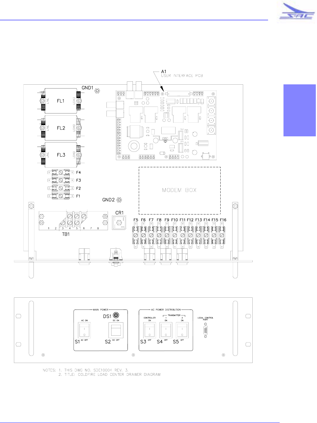
SD SERIES TRANSMITTER
65
•
•
•
•
•
•
SOUTHERN AVIONICS COMPANY
SECTION 2
2.4 SLE10004 - Load Center
SDE10004 - SD SERIES LOAD CENTER DRAWER DIAGRAM

SD SERIES TRANSMITTER
66
•
•
•
•
•
•
Southern Avionics Company
2.4.1 User Interface PCB
SLP10001 USER Interface PCB
This PCB is Located in the USER section which contains the AC and DC Power connection Terminal, the
EC filtering modules, the System Fusing and the Modem.
The USER Interface PCB combines in one central location circuitry which allows the Controller/Monitor
control over Antenna Switching in Dual systems and DCAD functions(DC Automatic Disconnect). It also furnishes
the Controller/Monitor with the input AC voltage level and current draw and the Battery system Voltage and current
readings if DC is Optioned.
It also provides convenient interconnect to the USER for MSK interfacing (Digital Global Positioning
Systems such as used by the US coast Guard)
In addition to this cross connects for voice input and phone line connections are present.

SD SERIES TRANSMITTER
67
•
•
•
•
•
•
SOUTHERN AVIONICS COMPANY
SECTION 2
SLP10006 - Assembly, PCB, User Interface
REFERENCE
DESIGNATOR COMPONENT DESCRIPTION
C1 1C551010 CAP, CERAMIC, .1MFD. 50V, 10%
C10 1C373300 CAP, 33M, 25V, TANT
C11 1C373300 CAP, 33M, 25V, TANT
C12 1C373300 CAP, 33M, 25V, TANT
C13 1C366800 CAP, 6.8M 25V TANT
C14 1C551010 CAP, CERAMIC, .1MFD. 50V, 10%
C15 1C366800 CAP, 6.8M 25V TANT
C16 1C561010 CAP, CERAMIC, 1MFD 50V 10%
C17 1C551010 CAP, CERAMIC, .1MFD. 50V, 10%
C2 1C373300 CAP, 33M, 25V, TANT
C3 1C551010 CAP, CERAMIC, .1MFD. 50V, 10%
C4 1C373300 CAP, 33M, 25V, TANT
C5 1C621040 CAP, 100MF, 100V ALUMINUM ELECTROYLTIC
C6 1C631010 CAP, 1000MF, 25V ALUMINUM ELECTROLYTIC
C7 1C373300 CAP, 33M, 25V, TANT
C8 1C373300 CAP, 33M, 25V, TANT
C9 1C551010 CAP, CERAMIC, .1MFD. 50V, 10%
CR1 1D400400 DIODE, RECT 400V 1A 30 DO41
CR10 1D066200 DIODE, SW 80V .040A
CR11 1D066200 DIODE, SW 80V .040A
CR12 1D005200 DIODE, GR 50V .050A
CR13 1D005200 DIODE, GR 50V .050A
CR2 1D400400 DIODE, RECT 400V 1A 30 DO41
CR3 1D400400 DIODE, RECT 400V 1A 30 DO41
CR4 1D400400 DIODE, RECT 400V 1A 30 DO41
CR5 1D400400 DIODE, RECT 400V 1A 30 DO41
CR6 1D400400 DIODE, RECT 400V 1A 30 DO41
CR7 1D540400 DIODE, RECT 400V 3A 267-02 SLCON
CR8 1D540400 DIODE, RECT 400V 3A 267-02 SLCON
CR9 1D440000 DIODE, ULTRAFAST RECOV RCT, 600V,4A
J1 56000010 CONN BNC PWB MT
J10A 50000005 CONN TERM BLK, 2 POS, FRONT INLET PC MT
J10B 50000005 CONN TERM BLK, 2 POS, FRONT INLET PC MT
J11 50000007 CONN TERM BLK, 3 POS, FRONT INLET PC MT
J12 50000007 CONN TERM BLK, 3 POS, FRONT INLET PC MT
J13 56000018 CONN, RIGHT ANGLE BNC PCB RECEPTACLE
JACK
J14 56000018 CONN, RIGHT ANGLE BNC PCB RECEPTACLE
JACK
J15 56000018 CONN, RIGHT ANGLE BNC PCB RECEPTACLE
JACK
J16 56000018 CONN, RIGHT ANGLE BNC PCB RECEPTACLE
JACK

SD SERIES TRANSMITTER
68
•
•
•
•
•
•
SOUTHERN AVIONICS COMPANY
J17A 50000005 CONN TERM BLK, 2 POS, FRONT INLET PC MT
J17B 50000005 CONN TERM BLK, 2 POS, FRONT INLET PC MT
J18 51000045 CONN, PC BOARD MOUNT RECEPTACLE
J19A 50000005 CONN TERM BLK, 2 POS, FRONT INLET PC MT
J19B 50000007 CONN TERM BLK, 3 POS, FRONT INLET PC MT
J19C 50000007 CONN TERM BLK, 3 POS, FRONT INLET PC MT
J2 56000010 CONN BNC PWB MT
J3 56000010 CONN BNC PWB MT
J4 56000010 CONN BNC PWB MT
J5 51000020 CONN., HEADER, .025 SQ. POSTS, 20 PIN
J6A 50000007 CONN TERM BLK, 3 POS, FRONT INLET PC MT
J6B 50000007 CONN TERM BLK, 3 POS, FRONT INLET PC MT
J7A 50000007 CONN TERM BLK, 3 POS, FRONT INLET PC MT
J7B 50000007 CONN TERM BLK, 3 POS, FRONT INLET PC MT
J8 50000007 CONN TERM BLK, 3 POS, FRONT INLET PC MT
J9 50000007 CONN TERM BLK, 3 POS, FRONT INLET PC MT
K1 9R190017 RELAY, SPDT, 12VDC, 30A, PCMT
K2 9R190017 RELAY, SPDT, 12VDC, 30A, PCMT
K3 9R190017 RELAY, SPDT, 12VDC, 30A, PCMT
K4 9R190017 RELAY, SPDT, 12VDC, 30A, PCMT
L1 1L000019 INDUCTOR, 220 UH @ 3.0 AMP
Q1 1T344000 XSTR NPN 250V 15MHZ TO205AD
Q2 1T344000 XSTR NPN 250V 15MHZ TO205AD
R1 1R641820 RES, 18K .25W 10 PCT CF
R10 1R738620 RES, 8.66K 1/4W 1% MF
R11 1RV41041 POT, 10K .75W CMT
R12 1R641820 RES, 18K .25W 10 PCT CF
R13 1RV41041 POT, 10K .75W CMT
R14 1RV41041 POT, 10K .75W CMT
R15 1R641820 RES, 18K .25W 10 PCT CF
R16 1R641820 RES, 18K .25W 10 PCT CF
R17 1RV41041 POT, 10K .75W CMT
R18 1RV41041 POT, 10K .75W CMT
R19 1R641820 RES, 18K .25W 10 PCT CF
R2 1R651020 RES, 100K .25W 10 PCT CF
R20 1RV41041 POT, 10K .75W CMT
R21 1R742221 RES, 22.1K .25W 1% MF
R22 1R746120 RES, 61.9K .25W 1% MF
R23 1RV41041 POT, 10K .75W CMT
R24 1R746120 RES, 61.9K .25W 1% MF
R3 1R633320 RES, 3.3K .25W 10 PCT CF
R4 1R739010 RES, 9.09K 1/8W 1% MF
R5 1R731020 RES, 1K 1/4W 1% MF
R6 1R641820 RES, 18K .25W 10 PCT CF
R7 1R651020 RES, 100K .25W 10 PCT CF
R8 1R633320 RES, 3.3K .25W 10 PCT CF
R9 1RV32030 POT, 2K .5W CMT
T1 1X000018 TRANSFORMER, 115/230V DUAL PRIMARY, 1VA,
MINATURE,

SD SERIES TRANSMITTER
69
•
•
•
•
•
•
SOUTHERN AVIONICS COMPANY
SECTION 2
T2 SLE30520 ASY XFMER 120T 06 MATL
U1 1U400100 IC QUAD 2-INP NOR
U2 1U324000 IC QUAD OP AMP
U3 1U257602 IC VOLT RGLTR 3A 1.23V TO 37V ADJ STEP
DOWN
U4 1U324000 IC QUAD OP AMP
U5 1U450400 IC, CMOS HEX VOLTAGE LEVEL SHIFTER
U6 1U766200 IC CMOS 8 PIN V CONV
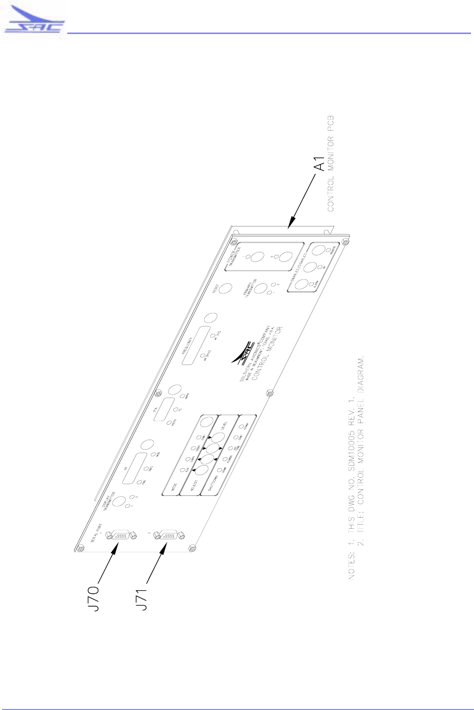
SD SERIES TRANSMITTER
70
•
•
•
•
•
•
SOUTHERN AVIONICS COMPANY
2.5 SLM10005 - Control Monitor Panel
SDM10005 - LOCAL CONTROL PANEL DIAGRAM

SD SERIES TRANSMITTER
71
•
•
•
•
•
•
Southern Avionics Company
SECTION 2
2.5.1 Local Control PCB
SLP10016 – Local Control
The Optional Local Control can be used as either a local or remote operating panel. The Local
Control is a microprocessor-based (Motorola M68HC11) unit offering partial control over the
controller / monitor and thereby the system. It offers similar functionality to a standard front
panel on older equipment.
Pushbuttons allow the user to select and or control the following:
Primary Transmitter Select (1 or 2)
Mode Select (ID, CONT or CARR)
Transmitter Displayed (1 or 2)
And view readings of: readings for:
PA Voltage
PA Current
PA Temperature
Forward Power
Reflected Power
Modulation%
Audio Frequency (tone)
RF Frequency
The user can adjust or set the:
Modulation Percentage
RF Power output level
RF ON/OFF
Enable/Disable Alarms
Select Local/Remote Control
When one of any pushbuttons is pressed except RESET, the 6811 processor sends a data
command to the Controller / Monitor through the serial communication port.
RESET forces Local Panel re-initialization.
The 7 segment led display update comes from the Controller / Monitor The displays provide the
3 following groups for reading:
1. RF Power:
Up to 4 digits display the Modulation%, forward power and reflected power.
2. Power Amplifier (P.A.):
Up to 3 digits Display the voltage, current and temperature.

SD SERIES TRANSMITTER
72
•
•
•
•
•
•
Southern Avionics Company
3. Frequency:
Up to 5 digits display the tone frequency (set) and RF frequency (measured).
The LED indicators simply display the system status. The Local Control receives a command
string from the Controller / Monitor and uses this to set the status indicators.
The complex logic needed to for pushbutton control and display is accomplished using
programmable gate-array logic.
The Local Control provides two serial communication ports (RS-232 / RS-485). The RS-
232 port is used locally for the Controller / Monitor serial port 1. The RS-485 port is connected
remotely to the Controller / Monitor port 1.

SD SERIES TRANSMITTER
73
•
•
•
•
•
•
SOUTHERN AVIONICS COMPANY
SECTION 2
SLP10016 - Assembly, PCB, Local Control
REFERENCE
DESIGNATOR COMPONENT DESCRIPTION
01 SRP10016 PCB, CONTROL MONITOR (COLD FIRE)
C01 6C451010 CAP, 1206, .1M, 50V, CERAMIC CHIP
C02 6C451010 CAP, 1206, .1M, 50V, CERAMIC CHIP
C03 6C451010 CAP, 1206, .1M, 50V, CERAMIC CHIP
C04 6C451010 CAP, 1206, .1M, 50V, CERAMIC CHIP
C05 6C451010 CAP, 1206, .1M, 50V, CERAMIC CHIP
C06 6C451010 CAP, 1206, .1M, 50V, CERAMIC CHIP
C07 6C451010 CAP, 1206, .1M, 50V, CERAMIC CHIP
C08 6C451010 CAP, 1206, .1M, 50V, CERAMIC CHIP
C09 6C451010 CAP, 1206, .1M, 50V, CERAMIC CHIP
C10 6C451010 CAP, 1206, .1M, 50V, CERAMIC CHIP
C11 6C451010 CAP, 1206, .1M, 50V, CERAMIC CHIP
C12 6C451010 CAP, 1206, .1M, 50V, CERAMIC CHIP
C13 6C451010 CAP, 1206, .1M, 50V, CERAMIC CHIP
C14 6C451010 CAP, 1206, .1M, 50V, CERAMIC CHIP
C15 6C451010 CAP, 1206, .1M, 50V, CERAMIC CHIP
C16 6C451010 CAP, 1206, .1M, 50V, CERAMIC CHIP
C17 6C451010 CAP, 1206, .1M, 50V, CERAMIC CHIP
C18 6C451010 CAP, 1206, .1M, 50V, CERAMIC CHIP
C19 6C451010 CAP, 1206, .1M, 50V, CERAMIC CHIP
C20 50000007 CONN TERM BLK, 3 POS, FRONT INLET PC MT
C21 6C410000 CAP, 1206 1.0UF, 25V CERAMIC
C22 6C451010 CAP, 1206, .1M, 50V, CERAMIC CHIP
C23 6C410000 CAP, 1206 1.0UF, 25V CERAMIC
C24 6C451010 CAP, 1206, .1M, 50V, CERAMIC CHIP
C25 6C386300 CAP, 3216 10UF 6.3V TANTALUM
C26 6C451010 CAP, 1206, .1M, 50V, CERAMIC CHIP
C27 6C412240 CAP, 1206, 22PF, 100V, CERAMIC CHIP
C28 6C412240 CAP, 1206, 22PF, 100V, CERAMIC CHIP
C29 6C451010 CAP, 1206, .1M, 50V, CERAMIC CHIP
C30 6C451010 CAP, 1206, .1M, 50V, CERAMIC CHIP
C31 6C451010 CAP, 1206, .1M, 50V, CERAMIC CHIP
C32 6C451010 CAP, 1206, .1M, 50V, CERAMIC CHIP
C33 6C451010 CAP, 1206, .1M, 50V, CERAMIC CHIP
C34 6C451010 CAP, 1206, .1M, 50V, CERAMIC CHIP
C35 6C451010 CAP, 1206, .1M, 50V, CERAMIC CHIP
C36 6C451010 CAP, 1206, .1M, 50V, CERAMIC CHIP
C37 6C451010 CAP, 1206, .1M, 50V, CERAMIC CHIP
C38 6C451010 CAP, 1206, .1M, 50V, CERAMIC CHIP
C39 6C451010 CAP, 1206, .1M, 50V, CERAMIC CHIP
C40 6C374700 CAP, 47 MFD, 16V, TANTALUM CHIP
C41 6C374700 CAP, 47 MFD, 16V, TANTALUM CHIP
C42 6C374700 CAP, 47 MFD, 16V, TANTALUM CHIP
C43 6C451010 CAP, 1206, .1M, 50V, CERAMIC CHIP
C44 6C451010 CAP, 1206, .1M, 50V, CERAMIC CHIP
C45 6C451010 CAP, 1206, .1M, 50V, CERAMIC CHIP

SD SERIES TRANSMITTER
74
•
•
•
•
•
•
SOUTHERN AVIONICS COMPANY
C46 6C451010 CAP, 1206, .1M, 50V, CERAMIC CHIP
C47 6C451010 CAP, 1206, .1M, 50V, CERAMIC CHIP
C48 6C451010 CAP, 1206, .1M, 50V, CERAMIC CHIP
C49 6C422100 CAP, 1206 2.2UF, 50V CERAMIC
DS01 1DL17000 LED, HIGH EFFICIENCY RED, 2.0 MA
DS02 1DL17000 LED, HIGH EFFICIENCY RED, 2.0 MA
DS03 1DL17000 LED, HIGH EFFICIENCY RED, 2.0 MA
DS04 1DL17000 LED, HIGH EFFICIENCY RED, 2.0 MA
DS05 1DL17000 LED, HIGH EFFICIENCY RED, 2.0 MA
DS06 1DL17000 LED, HIGH EFFICIENCY RED, 2.0 MA
DS07 1DL17000 LED, HIGH EFFICIENCY RED, 2.0 MA
DS08 1DL17000 LED, HIGH EFFICIENCY RED, 2.0 MA
DS09 1DL17000 LED, HIGH EFFICIENCY RED, 2.0 MA
DS10 1DL17000 LED, HIGH EFFICIENCY RED, 2.0 MA
DS11 1DL17000 LED, HIGH EFFICIENCY RED, 2.0 MA
DS12 1DL17000 LED, HIGH EFFICIENCY RED, 2.0 MA
DS13 1DL17000 LED, HIGH EFFICIENCY RED, 2.0 MA
DS14 1DL17000 LED, HIGH EFFICIENCY RED, 2.0 MA
DS15 1DL17900 LED, LOW CURRENT, GREEN, 4MW, 2MA
DS16 1DL17900 LED, LOW CURRENT, GREEN, 4MW, 2MA
DS17 1DL17000 LED, HIGH EFFICIENCY RED, 2.0 MA
DS18 1DL17000 LED, HIGH EFFICIENCY RED, 2.0 MA
DS19 1DL17000 LED, HIGH EFFICIENCY RED, 2.0 MA
DS20 1DL17000 LED, HIGH EFFICIENCY RED, 2.0 MA
DS21 1DL17000 LED, HIGH EFFICIENCY RED, 2.0 MA
DS22 1DL17000 LED, HIGH EFFICIENCY RED, 2.0 MA
DS27 1DL17000 LED, HIGH EFFICIENCY RED, 2.0 MA
DS28 1DL17000 LED, HIGH EFFICIENCY RED, 2.0 MA
DS29 1DL17000 LED, HIGH EFFICIENCY RED, 2.0 MA
DS30 1DL17000 LED, HIGH EFFICIENCY RED, 2.0 MA
DS31 1DL17000 LED, HIGH EFFICIENCY RED, 2.0 MA
DS32 1DL17000 LED, HIGH EFFICIENCY RED, 2.0 MA
J21 51000042 CONN, BREAKAWAY HEADER 156 CENTER 8 POS
J22 51000030 CONN., HEADER, BREAKAWAY, 10 POS DUAL ROW
J23 51000018 CONN., HEADER, .025 SQ. POSTS, 10 PIN
R01 6R224720 RES, 1206 4700 OHM 1/4W THICK FILM
R02 6R224720 RES, 1206 4700 OHM 1/4W THICK FILM
R03 6R224720 RES, 1206 4700 OHM 1/4W THICK FILM
R04 6R224720 RES, 1206 4700 OHM 1/4W THICK FILM
R06 6R224720 RES, 1206 4700 OHM 1/4W THICK FILM
R07 6R224720 RES, 1206 4700 OHM 1/4W THICK FILM
R08 6R224720 RES, 1206 4700 OHM 1/4W THICK FILM
R09 6R224720 RES, 1206 4700 OHM 1/4W THICK FILM
R10 6R224720 RES, 1206 4700 OHM 1/4W THICK FILM
R11 6R224720 RES, 1206 4700 OHM 1/4W THICK FILM
R12 6R224720 RES, 1206 4700 OHM 1/4W THICK FILM
R13 6R224720 RES, 1206 4700 OHM 1/4W THICK FILM
R14 6R224720 RES, 1206 4700 OHM 1/4W THICK FILM
R15 6R224720 RES, 1206 4700 OHM 1/4W THICK FILM
R16 6R224720 RES, 1206 4700 OHM 1/4W THICK FILM
R17 6R224720 RES, 1206 4700 OHM 1/4W THICK FILM
R18 6R231010 RES., 1206, 1K, 1/4W, 5%, THICK FILM CHIP
R19 6R224720 RES, 1206 4700 OHM 1/4W THICK FILM
R20 6R224720 RES, 1206 4700 OHM 1/4W THICK FILM

SD SERIES TRANSMITTER
75
•
•
•
•
•
•
SOUTHERN AVIONICS COMPANY
SECTION 2
R21 6R224720 RES, 1206 4700 OHM 1/4W THICK FILM
R22 6R231020 RES, 1206, 10M 1/4W 5% THICK FILM
R23 6R211020 RES, 1206 10K, 1/4W 5% THICK FILM
R24 6R211020 RES, 1206 10K, 1/4W 5% THICK FILM
R25 6R211020 RES, 1206 10K, 1/4W 5% THICK FILM
R26 6R211020 RES, 1206 10K, 1/4W 5% THICK FILM
R27 6R224720 RES, 1206 4700 OHM 1/4W THICK FILM
R28 6R221202 RES, 1206, 120 OHM 1/4W 5% THICK FILM
R29 6R221202 RES, 1206, 120 OHM 1/4W 5% THICK FILM
S01 9S901023 SWITCH, MOMENTORY, PUSH BUTTON SPST
S02 9S901023 SWITCH, MOMENTORY, PUSH BUTTON SPST
S03 9S901023 SWITCH, MOMENTORY, PUSH BUTTON SPST
S04 9S901023 SWITCH, MOMENTORY, PUSH BUTTON SPST
S05 9S901023 SWITCH, MOMENTORY, PUSH BUTTON SPST
S06 9S901023 SWITCH, MOMENTORY, PUSH BUTTON SPST
S07 9S901023 SWITCH, MOMENTORY, PUSH BUTTON SPST
S08 9S901023 SWITCH, MOMENTORY, PUSH BUTTON SPST
S09 9S901023 SWITCH, MOMENTORY, PUSH BUTTON SPST
S10 9S901023 SWITCH, MOMENTORY, PUSH BUTTON SPST
S11 9S901023 SWITCH, MOMENTORY, PUSH BUTTON SPST
S12 9S901023 SWITCH, MOMENTORY, PUSH BUTTON SPST
S13 9S901023 SWITCH, MOMENTORY, PUSH BUTTON SPST
S14 9S901023 SWITCH, MOMENTORY, PUSH BUTTON SPST
S15 9S901023 SWITCH, MOMENTORY, PUSH BUTTON SPST
S16 9S901023 SWITCH, MOMENTORY, PUSH BUTTON SPST
S17 9S901023 SWITCH, MOMENTORY, PUSH BUTTON SPST
S18 9S900031 SWITCH, SPST ROCKER RAISED 4 POS
TB21A 50000007 CONN TERM BLK, 3 POS, FRONT INLET PC MT
TB21B 50000007 CONN TERM BLK, 3 POS, FRONT INLET PC MT
U01 6U451101 IC, CMOS HIGH SPEED LOGIC BCD TO 7 SEG 16 PIN
U02 6RD31023 RESISTOR, NETWORK 1K, 16 PIN THICK FILM
U03 9L400000 DISPLAY, NUMERIC 0.3 (RED)
U04 6U451101 IC, CMOS HIGH SPEED LOGIC BCD TO 7 SEG 16 PIN
U05 6RD31023 RESISTOR, NETWORK 1K, 16 PIN THICK FILM
U06 9L400000 DISPLAY, NUMERIC 0.3 (RED)
U07 6U451101 IC, CMOS HIGH SPEED LOGIC BCD TO 7 SEG 16 PIN
U08 6RD31023 RESISTOR, NETWORK 1K, 16 PIN THICK FILM
U09 9L400000 DISPLAY, NUMERIC 0.3 (RED)
U10 6U451101 IC, CMOS HIGH SPEED LOGIC BCD TO 7 SEG 16 PIN
U11 6RD31023 RESISTOR, NETWORK 1K, 16 PIN THICK FILM
U12 9L400000 DISPLAY, NUMERIC 0.3 (RED)
U13 6U451101 IC, CMOS HIGH SPEED LOGIC BCD TO 7 SEG 16 PIN
U14 6RD31023 RESISTOR, NETWORK 1K, 16 PIN THICK FILM
U15 9L400000 DISPLAY, NUMERIC 0.3 (RED)
U16 6U451101 IC, CMOS HIGH SPEED LOGIC BCD TO 7 SEG 16 PIN
U17 6RD31023 RESISTOR, NETWORK 1K, 16 PIN THICK FILM
U18 9L400000 DISPLAY, NUMERIC 0.3 (RED)
U19 6U451101 IC, CMOS HIGH SPEED LOGIC BCD TO 7 SEG 16 PIN
U20 6RD31023 RESISTOR, NETWORK 1K, 16 PIN THICK FILM
U21 9L400000 DISPLAY, NUMERIC 0.3 (RED)
U22 6U451101 IC, CMOS HIGH SPEED LOGIC BCD TO 7 SEG 16 PIN
U23 6RD31023 RESISTOR, NETWORK 1K, 16 PIN THICK FILM
U24 9L400000 DISPLAY, NUMERIC 0.3 (RED)
U25 6U451101 IC, CMOS HIGH SPEED LOGIC BCD TO 7 SEG 16 PIN

SD SERIES TRANSMITTER
76
•
•
•
•
•
•
SOUTHERN AVIONICS COMPANY
U26 6RD31023 RESISTOR, NETWORK 1K, 16 PIN THICK FILM
U27 9L400000 DISPLAY, NUMERIC 0.3 (RED)
U28 6U451101 IC, CMOS HIGH SPEED LOGIC BCD TO 7 SEG 16 PIN
U29 6RD31023 RESISTOR, NETWORK 1K, 16 PIN THICK FILM
U30 9L400000 DISPLAY, NUMERIC 0.3 (RED)
U31 6U451101 IC, CMOS HIGH SPEED LOGIC BCD TO 7 SEG 16 PIN
U32 6RD31023 RESISTOR, NETWORK 1K, 16 PIN THICK FILM
U33 9L400000 DISPLAY, NUMERIC 0.3 (RED)
U34 6U451101 IC, CMOS HIGH SPEED LOGIC BCD TO 7 SEG 16 PIN
U35 6RD31023 RESISTOR, NETWORK 1K, 16 PIN THICK FILM
U36 9L400000 DISPLAY, NUMERIC 0.3 (RED)
U37 6U037300 IC, OCTAL TRANSPARENT D-TYPE LATCHES
U38 6RD31023 RESISTOR, NETWORK 1K, 16 PIN THICK FILM
U39 6U456401 IC, PROGRAMMABLE, 44 PIN TQFP
U40 6U037300 IC, OCTAL TRANSPARENT D-TYPE LATCHES
U41 6RD31023 RESISTOR, NETWORK 1K, 16 PIN THICK FILM
U42 6U037300 IC, OCTAL TRANSPARENT D-TYPE LATCHES
U43 6RD31023 RESISTOR, NETWORK 1K, 16 PIN THICK FILM
U44 6U456401 IC, PROGRAMMABLE, 44 PIN TQFP
U45 6U037300 IC, OCTAL TRANSPARENT D-TYPE LATCHES
U46 6RD31023 RESISTOR, NETWORK 1K, 16 PIN THICK FILM
U47 6U509000 IC, CHANNEL ANALOG MULTIPLEXER
U48 6U325301 IC, DUAL MULTIPLEXER/DEMIULPLEXER BUS SWITCH
U49 1U687110 IC HCMOS 8-BIT MICONTR
U50 6U037300 IC, OCTAL TRANSPARENT D-TYPE LATCHES
U51 6U742212 IC, DUAL INVERTING, NON-INVERTING OCTAL BUFFER
U52 6U037300 IC, OCTAL TRANSPARENT D-TYPE LATCHES
U53 6U742212 IC, DUAL INVERTING, NON-INVERTING OCTAL BUFFER
U54 6U037300 IC, OCTAL TRANSPARENT D-TYPE LATCHES
U55 6U742212 IC, DUAL INVERTING, NON-INVERTING OCTAL BUFFER
U56 6U742212 IC, DUAL INVERTING, NON-INVERTING OCTAL BUFFER
U57 6U037300 IC, OCTAL TRANSPARENT D-TYPE LATCHES
U58 6U037300 IC, OCTAL TRANSPARENT D-TYPE LATCHES
U59 6U742212 IC, DUAL INVERTING, NON-INVERTING OCTAL BUFFER
U60 6U037300 IC, OCTAL TRANSPARENT D-TYPE LATCHES
U61 6U020800 IC, CMOS RS-232 DRIVER/RECEIVER
U62 1U751790 IC, DIFF DRIVER/RECEIVER PAIR, 8 DIP
W01 304A0000 WIRE 22 AWG SOLID TINNED
W02 304A0000 WIRE 22 AWG SOLID TINNED
W03 304A0000 WIRE 22 AWG SOLID TINNED
XJ23A 5A000030 LOCK, EJECTOR HOOK, SHORT
XJ23B 5A000030 LOCK, EJECTOR HOOK, SHORT
XU49 9S581002 SOCKET, PLCC, 52 PIN
Y1 1Y491520 CRYSTAL, 4.9152 MHZ

SD SERIES TRANSMITTER
77
•
•
•
•
•
•
Southern Avionics Company
SECTION 2
2.5.2 Audio PCB
SLP10020 OPTIONAL AUDIO PCB (AWOS)
The Audio PCB is an OPTIONAL addition to the normal system which allows the user to broadcast AWOS
announcements. The Option is implemented as a plug in piggyback board to the Digital I/O PCB and consists of four
sections as follows:
Voice Amplifier
Automatic Gain Control
Chebychev Passband Filter
Voice Detector
The Voice amplifier takes the nominal -17dBm signal level and boosts it to a level useable by the AGC
section.
It is common mode balanced and its Gain is adjustable.
The AGC circuit is responsible for modulation limiting. It is adjusted to "capture" the level at -17dBm and
output a constant modulation level to the Digital I/O PWM section up to levels exceeding +10 dBm. This section
prevents inadvertent over modulation of the voice signal, and is necessary since the Controller / Monitor has no
control over user input.
The Chebychev Passband filter is designed for 300 to 3000 Hz. The output at 4000 Hz is down more than 45
dB ensuring any out of band audio signals from the USER will not cause adjacent channel interference.
The Voice Detector has two functions. It detects the presence of an announcement sequence and
automatically attenuates the Keying tone level down to 20% modulation. The announcement level is summed with
the Keying tone level and set to achieve 95% composite modulation. This action prevents overmodulation and allows
the announcement to be heard over the beacon Morse code IDENT tones. It also signals the Controller /Monitor
which in turn temporarily suspends Modulation Alarms since the IDENT tone level is dropped below the alarm
threshold.

SD SERIES TRANSMITTER
78
•
•
•
•
•
•
Southern Avionics Company
2.5.1 Filter/Bridge PCB
SLP10002 - The Filter/Bridge PCB
The Filter/Bridge includes a broadband toroidal impedance transformer, a seven pole Butterworth low pass
filter, a broadband RF power bridge, modulation envelope detector and associated level sampling and fault latching
circuitry.
The Impedance transformer receives as input the RF Power Amplifiers Class D output and impedance matches it to
the 50Ohm Butterworth Low Pass Filter, which is configured for optimum characteristics via simple jumpers for the
frequency band in use. The sinusoidal 50Ohm output of the Filter is Fed then fed through the RF power bridge which
reports readings of Forward and Reflected RF Power to the Controller / Monitor. The Controller / Monitor then
normalizes and calibrates the power curve and calculates SWR. Fault latches are also set up to report High reflected
power or RF over-current conditions for immediate action via a fault interrupt structure. A sample of the final RF
output envelope is detected and sent back to the Controller / Monitor where other circuitry derives Vmax/Vmin
information for modulation percentage calculation via Controller / Monitor firmware.

SD SERIES TRANSMITTER
79
•
•
•
•
•
•
SOUTHERN AVIONICS COMPANY
SECTION 2
SLP10002/01 - Assembly, PCB Filter/Bridge (Standard Band)
REFERENCE
DESIGNATOR COMPONENT DESCRIPTION
01 SLP10002 PCB, FILTER / BRIDGE
C01 1C135190 CAP, 5100P 1000V DSM
C02 1C131090 CAP 1000P 1000V DSM
C03 1C132090 CAP, 2000P 1000V DSM
C04 1C136890 CAP, 6800P 1000V DSM
C05 1C126890 CAP, 680P 1000V DSM
C06 1C132090 CAP, 2000P 1000V DSM
C07 1C133390 CAP, 3300P 1000V DSM
C08 1C138290 CAP, 8200P 1000V DSM
C09 1C141090 CAP, 10,000P 1000V DSM
C10 1C132090 CAP, 2000P 1000V DSM
C11 1C131090 CAP 1000P 1000V DSM
C12 1C133990 CAP, 3900P 1000V DSM
C13 1C135190 CAP, 5100P 1000V DSM
C14 1C135190 CAP, 5100P 1000V DSM
C15 1C131090 CAP 1000P 1000V DSM
C16 1C136890 CAP, 6800P 1000V DSM
C17 1C132090 CAP, 2000P 1000V DSM
C18 1C126890 CAP, 680P 1000V DSM
C19 1C132090 CAP, 2000P 1000V DSM
C20 1C133390 CAP, 3300P 1000V DSM
C21 1C551010 CAP, CERAMIC, .1MFD. 50V, 10%
C22 1C073310 CAP, 33M 50V ELCTLT
C23 1C551010 CAP, CERAMIC, .1MFD. 50V, 10%
C24 1C551010 CAP, CERAMIC, .1MFD. 50V, 10%
C25 1C551010 CAP, CERAMIC, .1MFD. 50V, 10%
C26 1C073310 CAP, 33M 50V ELCTLT
C27 1C551010 CAP, CERAMIC, .1MFD. 50V, 10%
C28 1C124770 CAP, 470P 500V DSM
C29 1C103070 CAP, 3.0PF 500V DSM
C30 1C103070 CAP, 3.0PF 500V DSM
C31 1C551010 CAP, CERAMIC, .1MFD. 50V, 10%
C32 1C551010 CAP, CERAMIC, .1MFD. 50V, 10%
C33 1C122270 CAP, 220P 500V DSM
C34 1C122270 CAP, 220P 500V DSM
C35 1C621040 CAP, 100MF, 100V ALUMINUM ELECTROYLTIC
C36 1C631010 CAP, 1000MF, 25V ALUMINUM ELECTROLYTIC
CR1 1D005200 DIODE, GR 50V .050A
CR2 1D005200 DIODE, GR 50V .050A
CR3 1D005200 DIODE, GR 50V .050A
CR4 1D440000 DIODE, ULTRAFAST RECOV RCT, 600V,4A
L01 SLE55480 CSY COIL FLTR 250W 22T .D :10
L02 SLE45690 ASY COIL SPA FLTR :10

SD SERIES TRANSMITTER
80
•
•
•
•
•
•
SOUTHERN AVIONICS COMPANY
L03 SLE45700 ASY COIL SPA FLTR :10
L04 SLE55490 ASY COIL FLTR 250W 22T .D:10
L05 1L000017 INDUCTOR, MOLDED, SHILDED RF, 33000 uF
L06 1L000017 INDUCTOR, MOLDED, SHILDED RF, 33000 uF
L07 1L000017 INDUCTOR, MOLDED, SHILDED RF, 33000 uF
L08 1L000019 INDUCTOR, 220 UH @ 3.0 AMP
P01 51000041 CONN, HEADER 48 PIN PLUG, RT ANGLE
P02 51000041 CONN, HEADER 48 PIN PLUG, RT ANGLE
R01 1R141820 RES, 18K 1PCT .25W MF
R02 1R731020 RES, 1K 1/4W 1% MF
R03 1R731020 RES, 1K 1/4W 1% MF
R04 1R751020 RES, 100K .25W 1% MF
R05 1R761020 RES, 1 MEG OHM 1/4W 1% MF
R06 1R741020 RES, 10K 1/4W 1% MF
R07 1RV41041 POT, 10K .75W CMT
R08 1R751020 RES, 100K .25W 1% MF
R09 1R761020 RES, 1 MEG OHM 1/4W 1% MF
R10 1R741020 RES, 10K 1/4W 1% MF
R11 1RV41041 POT, 10K .75W CMT
R12 1R741020 RES, 10K 1/4W 1% MF
R13 1R751020 RES, 100K .25W 1% MF
R14 1R141820 RES, 18K 1PCT .25W MF
R15 1R731020 RES, 1K 1/4W 1% MF
R16 1R731020 RES, 1K 1/4W 1% MF
R17 1R734721 RES, 4.7K 1/4W 1 % MF
R18 1R751020 RES, 100K .25W 1% MF
R19 1R741020 RES, 10K 1/4W 1% MF
R20 1R741020 RES, 10K 1/4W 1% MF
R21 1RV15030 POT, 50 OHM 1/2W TOP ADJUST
R22 1RV15030 POT, 50 OHM 1/2W TOP ADJUST
R23 1R729320 RES, 931 OHM 1/4W 1% MF
R24 1R738220 RES, 8.2K 1/4W 1 % MF AXIAL
S01 9S902004 SWITCH, SPST DIP KEYBOARD
T1 SLE10014 ASSY, TRANSFORMER IMPEDANCE FILTER/BRIDGE
T2 1X000038 TRANSFORMER, CURRENT SENSE ENCAPSULATED
U01 1U324000 IC QUAD OP AMP
U02 1U339000 IC LOW POWER OFFSET VOLTAGE QUAD
COMPARATOR
U03 1U404300 IC QUAD NOR R-S LCH
U04 1U257602 IC VOLT RGLTR 3A 1.23V TO 37V ADJ STEP DOWN
XU4 9H180001 HEATSINK, LOW PROFILE, FOR T0-220
XU4A 9I550000 INSULATOR, TERMASIL, FOR T0-220

SD SERIES TRANSMITTER
81
•
•
•
•
•
•
SOUTHERN AVIONICS COMPANY
SECTION 3
3 INSTALLATION AND OPERATION
INSTALLATION
1.0 TEST EQUIPMENT REQUIRED
1.1 Calibrated 3 1/2 Digit Voltmeter
1.2 Calibrated Dual Trace Oscilloscope
1.3 Calibrated Frequency Counter (accurate to ± 1 Hz)
1.4 250 Watt, 50Ω Non-Inductive dummy load
2.0 UNPACKING & MOUNTING
2.1 Remove the Transmitter cabinet from its shipping container , open the front panel, and remove any
shipping material that may be included. Make a careful inspection looking for obvious shipping
damage. Remove any foreign material that may have shaken loose.
2.2 Some PC boards are shipped in separate boxes. Individually unpack and inspect them for any obvious
shipping damage. Check the connectors for any bent pins. Be sure to do this before attempting to
plug any of the PCB's in.
2.3 Assuming the transmitter is not to be pre-tested in a lab facility, physically mount the Cabinet to its
permanent structure. See drawing SDE10018, Page 5, for mounting hole dimensions.
3.0 PLUG INS
3.1 See the System installation drawings, SDF31002 , Pages 9 and 10, for additional information
pertaining to the following steps.
3.2 Remove the front panel exposing the Controller/ Monitor, Transmitter 1and User Sections
3.3 Remove the Controller Monitor cover panel and set it aside
3.4 Verify that the Monitor/Controller, Analog I/O and Digital I/O are installed and well seated in the
correct slots according to the drawing.
3.5 Unpack the smaller 3U sized Low Voltage Power supply PCB (SLP10017) and examine it closely for
any damage.
3.6 Check JP1 and JP2 on this PCB and verify they set correctly for the input voltage being used.
3.7 Refer to Drawing SDF31002, Page 10, and insert the LVPS PCB (SLP10017) into the left-most
slot. The board insertion must be exactly as shown in the drawing or serious damage may occur.
3.8 Remove the Transmitter 1 cover panel
3.9 Unpack the Transmitter 1 PCBs and examine them closely for any damage
3.10 Install the RF Amplifier PCB (SLP10001) in slot #2 or right next to the already installed Filter /
Bridge PCB (SLP10002) . See Drawing
JP1 JP2
115 VAC A B
230VAC B A

SD SERIES TRANSMITTER
82
•
•
•
•
•
•
SOUTHERN AVIONICS COMPANY
3.11 Install the PA Power Supply PCB (SLP10003) in slot # 3 or the last slot from the right.
3.12 On the right hand side of the Section, look at the RF Mother Board (SLP10004) and verify the
transformer connectors are seated properly.
3.13 Replace the Transmitter 1 cover panel
4.0 USER WIRING
4.1 The USER main AC breaker should be rated for 30 amps
4.2 Remove the mounting screws from the USER section and pull it forward on its mounting guides
sufficient to allow access to the bottom rear cabling ports.
4.3 Utilizing the (SLM 25000/25040) installation kit route the AC, DC, and Coupler wiring into the
bottom rear access holes.
4.4 Trim the excess wiring length to neatly reach the their individual connection points as cited below
4.5 Terminate the ends of the wires using the connectors supplied with the installation kit.
4.6 Connect a good Earth ground to the brass grounding terminal located on the bottom of the Cabinet
4.7 Locate the Main Power Connector TB1
4.8 Connect AC mains L1 to user section TB1-1 (115/230 VAC Hot )
4.9 Connect AC mains L2 to user section TB1-2 (115/230 VAC Neutral or Hot
4.10 Connect AC mains GND to user section TB1-3 ( AC Power GND )
4.11 Connect the Battery I (current charge/discharge) Sample shielded cable center wire to TB1-4
4.12 Connect the Battery I (current charge/discharge) Sample shield to TB1-3 (GND)
4.13 Connect 48V Battery + to TB1-5
4.14 Connect 48V Battery - to TB1-6
4.15 Connect Modular telephone jack to Line In on the US Robotics modem.
4.16 Locate the USER Interface PCB.
4.17 If no modular style plug is available, a 4 wire conventional drop cable may be connected to TB8 (
old J17) and the short modular jumper furnished by US Robotics connected from LINE-IN in of the
modem to J65 (old J18 ). The connections are:
Tip or Green wire to TB8-1
Ring or Red wire to TB8-2
Sleeve or Yellow wire to TB8-3
Ground or Black wire to TB8-4
4.18 Connect the coupler +12V supply wire to TB4 -3
4.19 Connect the coupler GND wire to TB4-2
4.20 If the system uses MSK externally supplied RF signal connect MSK-1 to J61(old J13) and MSK-2 to
J59 (old J14)
4.21 Dress and tie wrap the wires back to the end of the user panel.
4.22 Slowly push the USER drawer back in place.
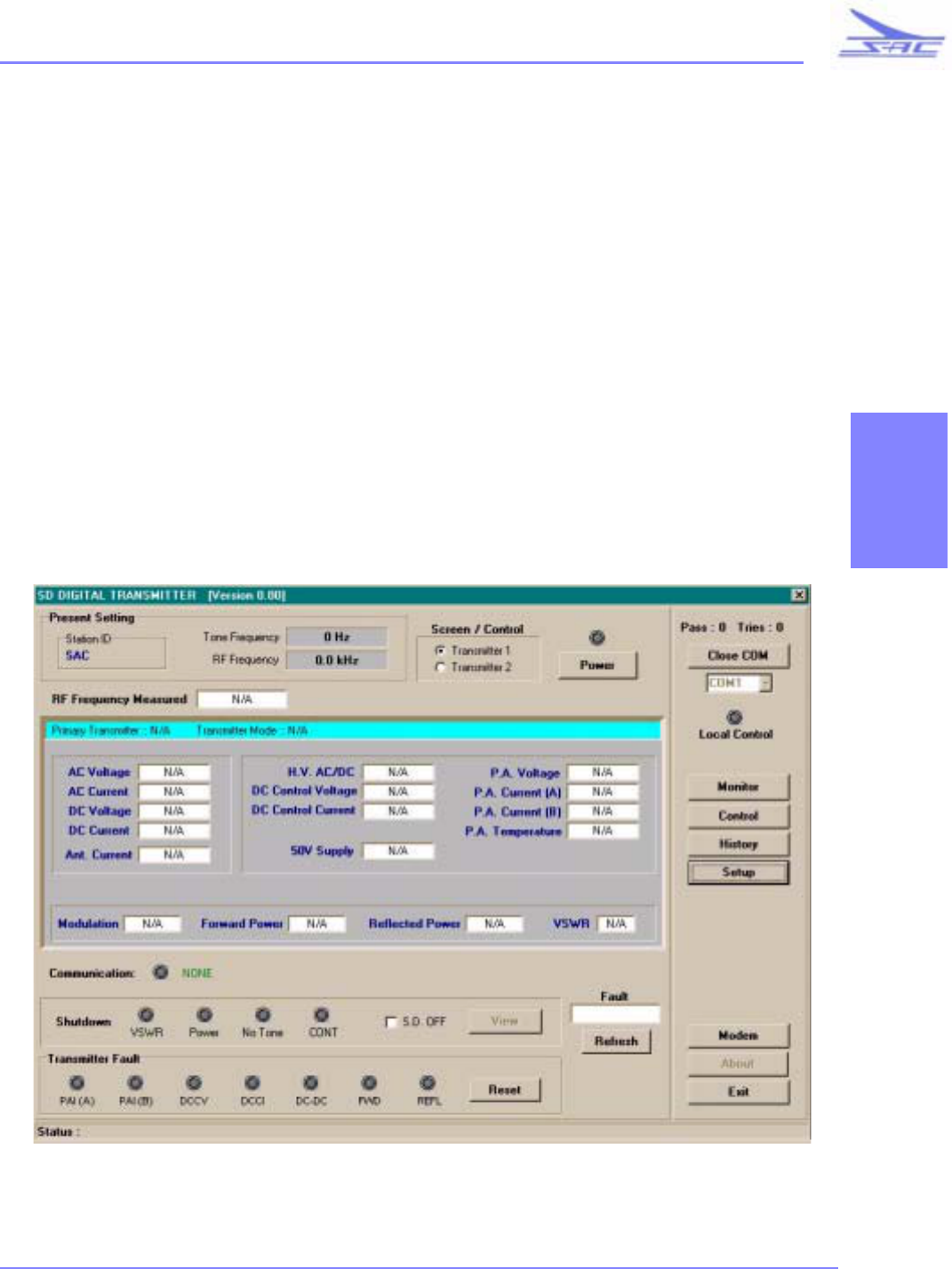
SD SERIES TRANSMITTER
83
•
•
•
•
•
•
SOUTHERN AVIONICS COMPANY
SECTION 3
4.23 If a 50 ohm Dummy load is available connect it to The N type RF output connector on the bottom of
the cabinet for initial testing and operational verification.
5.0 PC HOOKUP AND SOFTWARE INSTALLATION
5.1 A Desk-top or Laptop PC capable of running either Windows 98 or later version Microsoft operating
system is suitable for use as a local or remote control platform. Set the PC up near the transmitter.
5.2 Connect one end of a null modem RS232 cable or a standard RS232 cable with a null modem
adapter to SERIAL PORT #1 on the PC
5.3 Locate the left hand Controller/Monitor PCB which is the second board from the left in the controller
3U Section .
5.4 Connect the other end of the RS232 cable to the Local Control Port, a DB9 connector on the front of
the USER panel an the right hand side. (see drawing SDE 10004)
5.5 Start the computer and while it is booting up, locate the USER software which is included with each
system shipped in an appropriately labeled protective package.
5.6 Load the software on the PC, following the enclosed instruction sheet which will alert you to any last
minute changes that need attention.
5.7 Run the software and the SD DIGITAL TRANSMITTER window will open.
5.8 You will be required to enter a password. If no password is entered no operational changes will be
allowed. Monitoring, however, will still be available.
6.0 CONTROLLER/MONITOR POWER UP

SD SERIES TRANSMITTER
84
•
•
•
•
•
•
SOUTHERN AVIONICS COMPANY
6.1 See drawing SDE10004
6.2 Turn on the Site AC breaker.
6.3 On the USER panel in the MAIN POWER section , Switch AC to ON and observe the switch lights
up.
6.4 Leave the DC switch OFF for now.
6.5 On the USER panel in the AC POWER DISTRIBUTION section , Switch Controller to ON and
observe the switch lights up.
6.6 Observe the illumination of DS1 and DS2 the two green LEDS on the Digital I/O PCB (SLP10009)
indicating the presence of +5 and +12 volts respectively.
6.7 On the Low Voltage Power Supply PCB (SLP10017 ) Meter the following to GND (TP0) and verify
the tolerances
6.7.1 TP1 = 5.0 ± 0.25 VDC
6.7.2 TP2 = -11.4 ± 0.6 VDC
6.7.3 TP3 = 12.0 ± 0.6 VDC
NOTE: If any of these voltages are out of tolerance and require either repair or adjustment, a modified system
alignment will be required before proceeding. See the Maintenance section for more details.
7.0 SYSTEM SITE CONFIGURATION
7.1 On the PC in the SD DIGITAL TRANSMITTER window just below the Open COM control there is
a pull down menu to select a different serial port if desired. Click on the port you want then Click on
Open COM.
7.2 If opening the port was successful a bell will sound and the name of the control will change to
CLOSE COM
NOTE:Clicking again will close the Port so be careful not to double click. Click CLOSE COM only
when you are finished communicating with the system
7.3 The Morse Code ID sequence, Code Timing, Key tone Frequency, and RF frequency must now all
be set according to the Site License. On the PC in the SD DIGITAL TRANSMITTER window Click
on Set up.
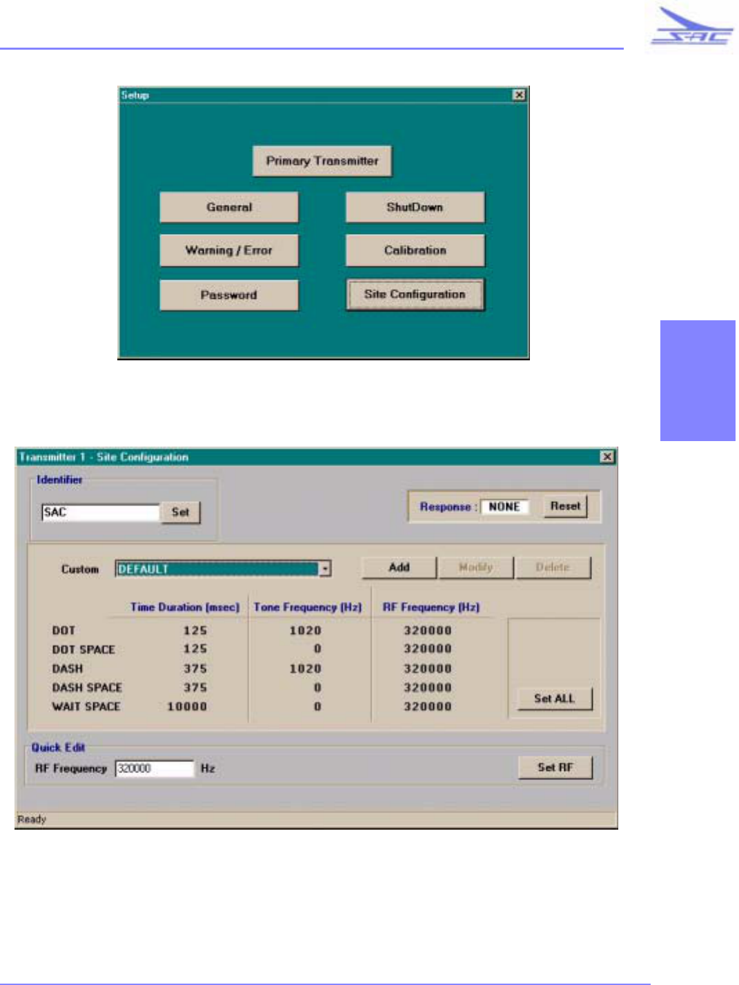
SD SERIES TRANSMITTER
85
•
•
•
•
•
•
SOUTHERN AVIONICS COMPANY
SECTION 3
7.4 From the menu select Site Configuration
7.5 A popup window called Transmitter 1 Site Configuration will open. In this window you may choose
to add a custom configuration to the selection list or simply accept the default profile and modify it as
follows:
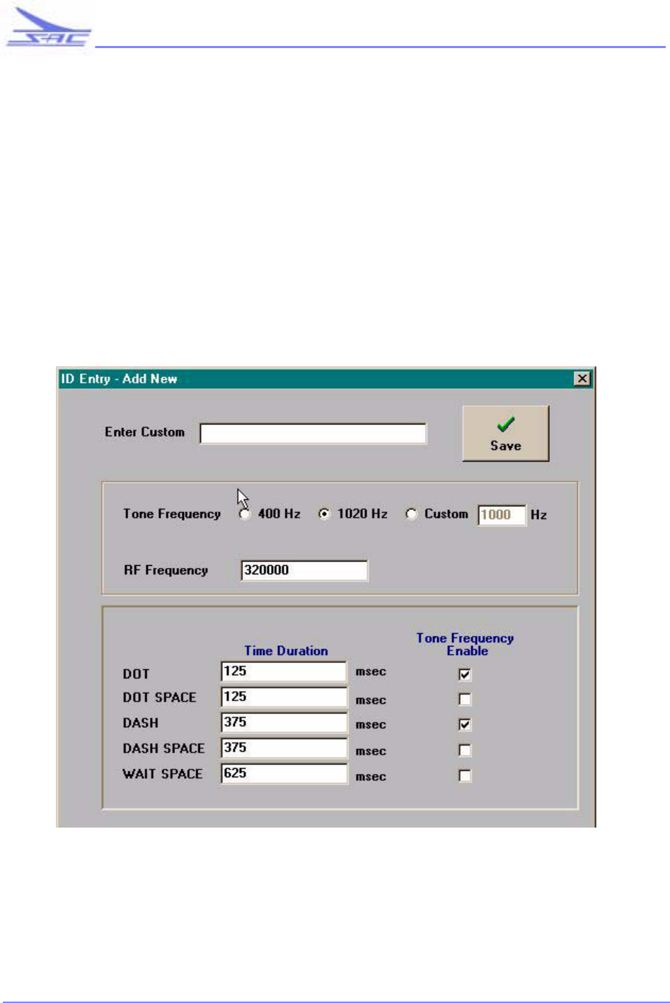
SD SERIES TRANSMITTER
86
•
•
•
•
•
•
SOUTHERN AVIONICS COMPANY
7.5.1 To modify the existing default setting
7.5.1.1. Click in the Identifier white space and change the ID to the new ID then click Set.
7.5.1.2. The new ID will be sent to the CF and the response window will read PASS when it is
accepted
7.5.1.3. Click in the Quick Edit RF Frequency white space, enter the new frequency then click on
Set RF
7.5.1.4. The new RF Frequency will be sent to the CF and the response window will read PASS
when it is accepted
7.5.2 To Add a new Custom configuration Click on Add and a popup window will appear.
7.5.2.1. Enter a custom name for this configuration. (Note that pressing enter will have no effect )
7.5.2.1.1. Select one of the 2 default tone frequencies or enter any frequency manually
between 300 and 3000 Hz.
7.5.2.1.2. Enter the RF frequency for this site.
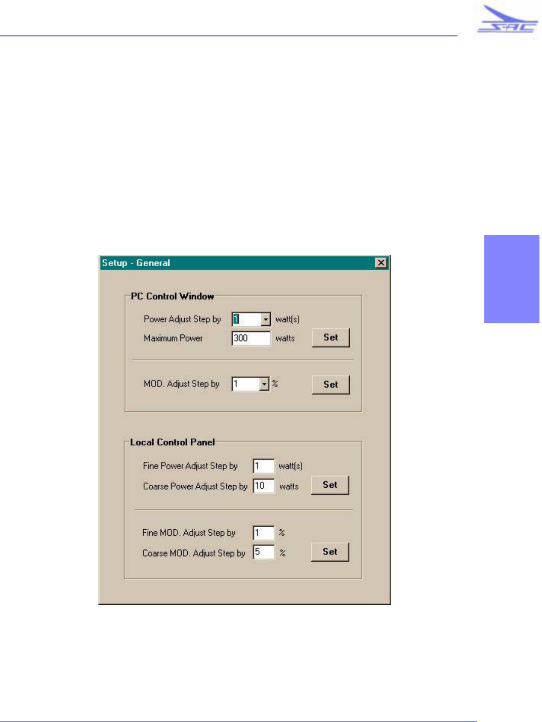
SD SERIES TRANSMITTER
87
•
•
•
•
•
•
SOUTHERN AVIONICS COMPANY
SECTION 3
7.5.2.1.3. Mark/Space timing changes and tone enables are optional. They will default to the
industry standard however they can be customized for special test sequences or
minor adjustments necessary in certain countries. Simply change the values to
those desired by clicking in the white space and entering a new value.
7.5.2.1.4. Click Save. The window will close returning to the Site Configuration window.
The saved configuration will be in the custom window
7.5.2.1.5. Click on Set ALL and the new configuration will be sent to the Controller/Monitor
7.6 Having chosen and accomplished one of the above methods, close the Transmitter 1 Site
Configuration window returning to the SETUP window.
7.7 In the Setup window, click on General, opening the general setup window
7.7.1 The PC control and Local Control sections allow the USER to define the fineness of control.
The Maximum Power is Factory set to coincide with the maximum power allowed by the site.
A lower power may be entered if the user chooses to run at a lower power. Firmware settings
will not allow more power to be output than what was licensed. Accept the defaults for now
and click on the X to exit
7.8 In the Setup window, click on Primary Transmitter, opening the selection window
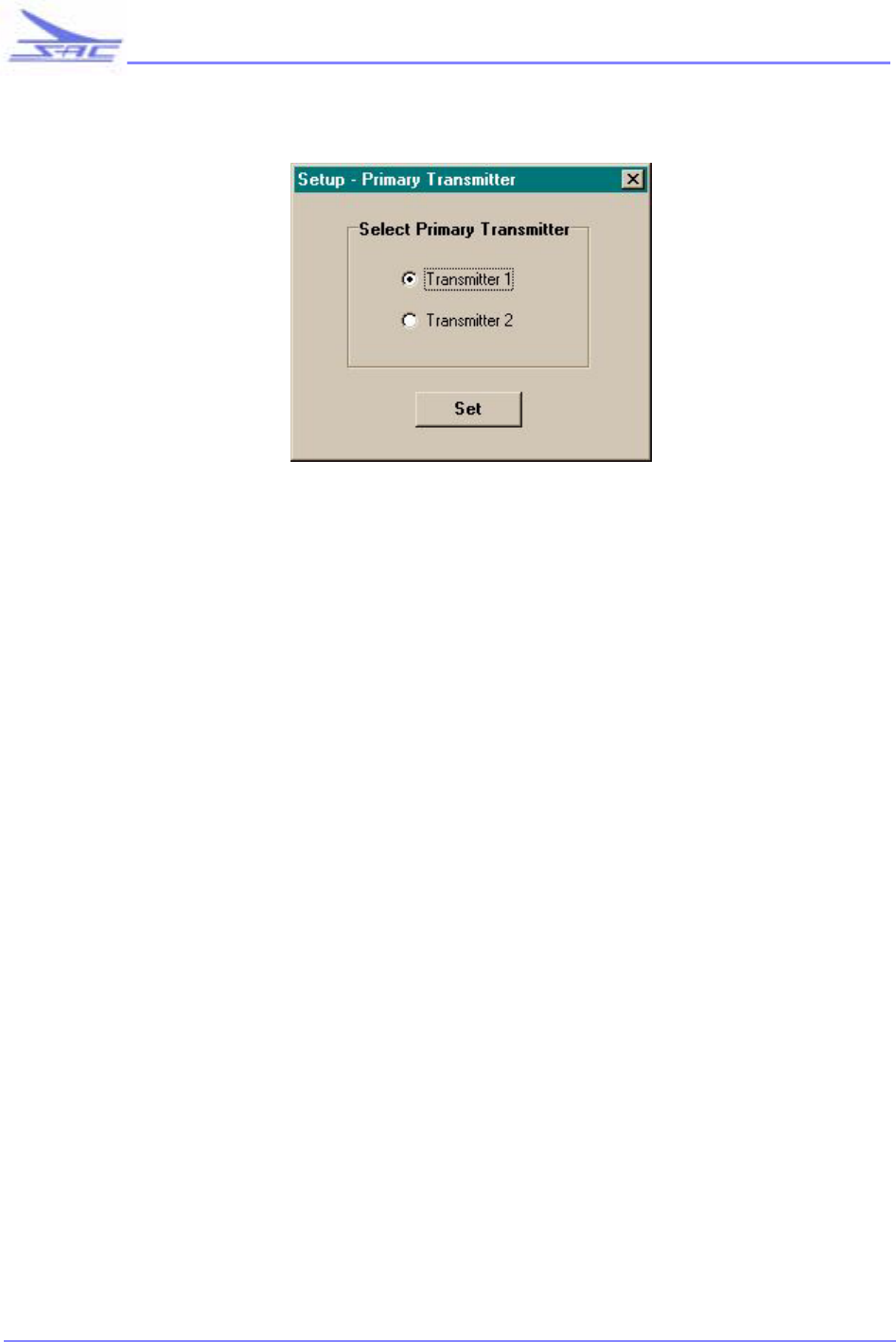
SD SERIES TRANSMITTER
88
•
•
•
•
•
•
SOUTHERN AVIONICS COMPANY
7.8.1 Accept the Default setting. If this were a Dual site you could choose which transmitter is
Primary here. Just Click on Set to return to the Set up menu
7.9 In the Setup window, click on Shutdown , opening the shutdown option window
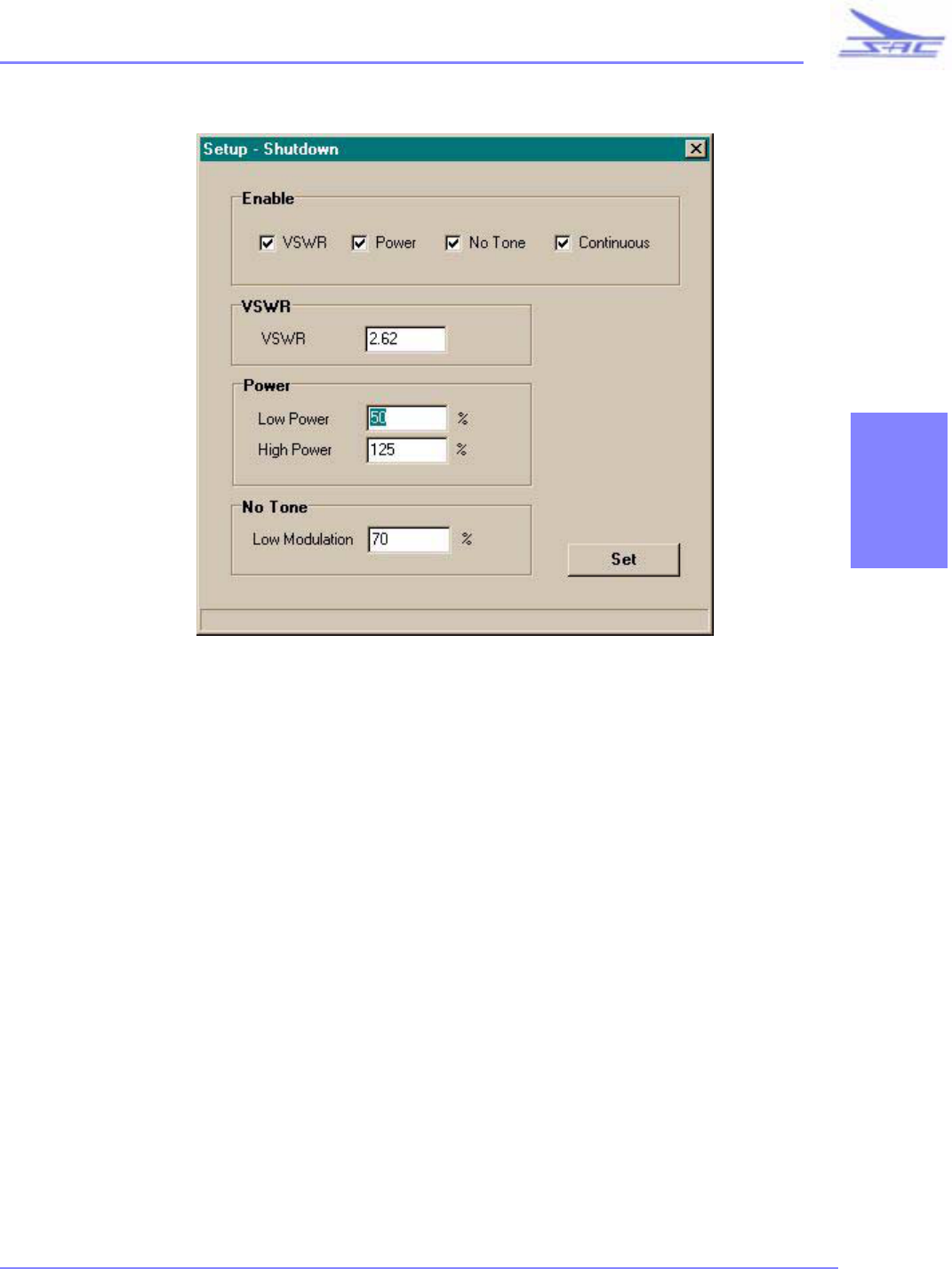
SD SERIES TRANSMITTER
89
•
•
•
•
•
•
SOUTHERN AVIONICS COMPANY
SECTION 3
7.9.1 This section allows you to set the criterion for some of the shutdown alarms and to enable or
disable them for test purposes. Since we will be testing a new installation, click to remove the
checkmarks from VSWR, Power, No Tone, and Continuous, thus disabling them. Click on
Set returning to the Setup window
7.10 In the Setup window, click on Warning/Error opening the warning /error list.
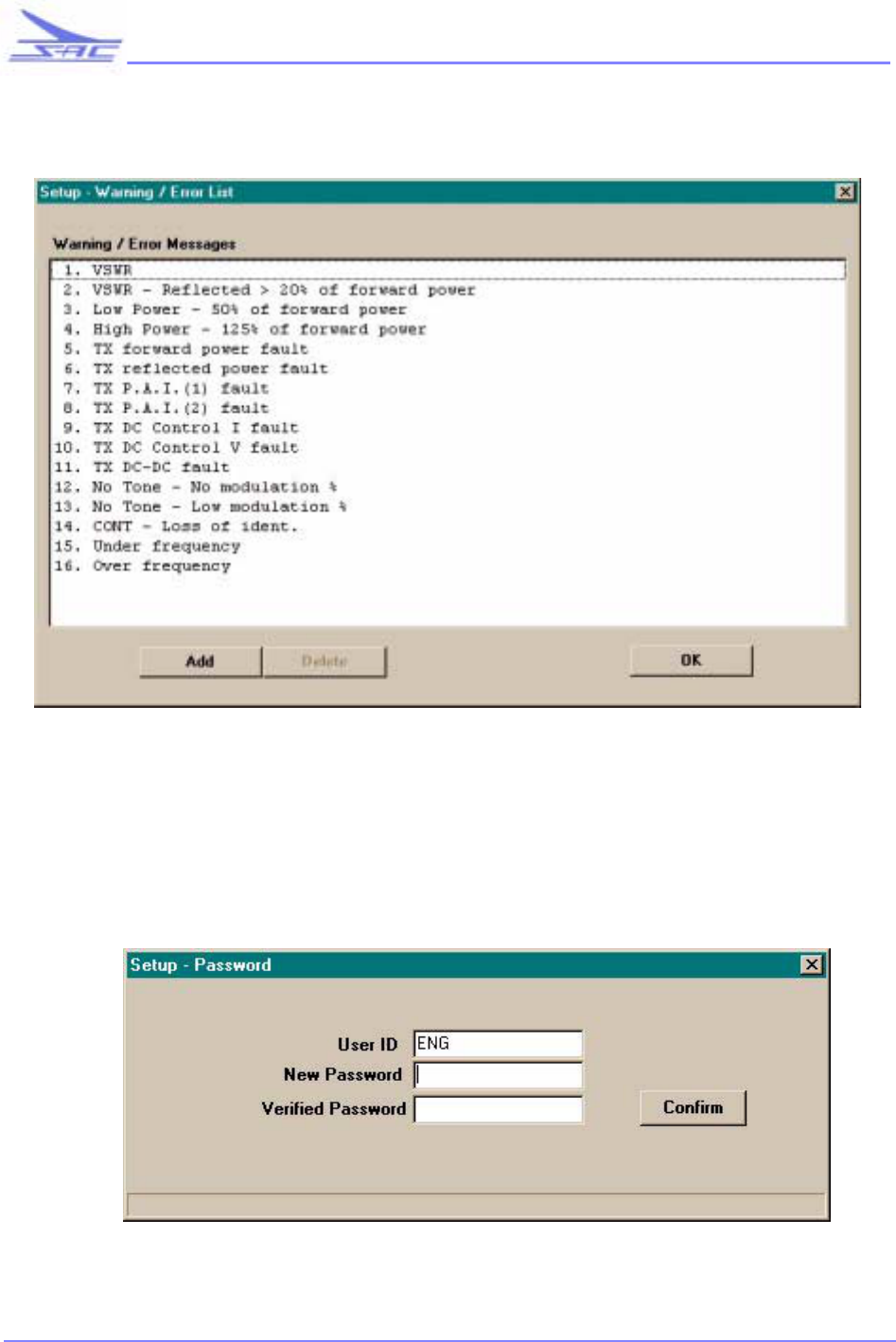
SD SERIES TRANSMITTER
90
•
•
•
•
•
•
SOUTHERN AVIONICS COMPANY
7.10.1 This list affords the USER a way to customize the error messages, re-writing them their native
language for instance. You can change these now or accept the default messages. Click on
OK to exit back to Setup
7.11 In the Setup window, click on Password opening the password window.
7.11.1 When the installation is complete a password should be entered here securing the site from
un-authorized access to system configuration while still allowing casual monitoring.

SD SERIES TRANSMITTER
91
•
•
•
•
•
•
SOUTHERN AVIONICS COMPANY
SECTION 3
7.11.2 For now no action is required so just press X to exit.
7.12 Press X to escape out of the Set up menu.
7.13 Verify the Correct Station ID, RF Frequency and Tone Frequency is displayed in the "Present Setting
" section of the main screen. The middle monitoring section of the main screen will be indicating N/
A in all of its display areas. (white boxes)
7.14 Having followed all the preceding steps the system should now be configured with the proper
parameters to allow an operational check
8.0 OPERATIONAL CHECK
Note: The SD 250 is a Direct Digital Synthesis (DDS) based microprocessor controlled transmitter
operating class D through broadband Butterworth filters. The system is quite adjustment free because of
this , however there are checkpoints that should be verified with Calibrated test equipment to ensure
proper operation.
8.1 Turn the AC POWER DISTRIBUTION TRANSMITTER 1 Switch (S4) on. It should illuminate.
8.2 On the PC click on Monitor, then select Transmitter #1 and click on Ready. This signals the
Controller /Monitor to begin sending transmitter data to the PC.
8.3 Click on Power and verify the following:
8.3.1 The High Voltage ON relay and the inrush circuit relay on the PA Power Supply PCB in the
RF section will activate in sequence
8.3.2 DS2 on the RF mother board will illuminate indicating the presence of High Voltage.
8.3.3 DS1 on the PA Power Supply PCB will illuminate indicating the presence of High Voltage.
8.3.4 The data fields on the PC main window screen will fill with system wide information similar
to that shown in the following screen capture
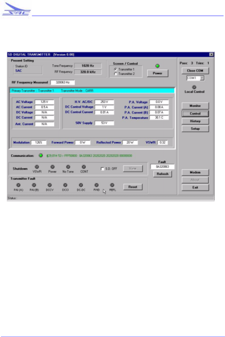
SD SERIES TRANSMITTER
92
•
•
•
•
•
•
SOUTHERN AVIONICS COMPANY
8.3.5 Note that DC Voltage, DC Current and Antenna Current readings are not shown. They are
signals fed in from external sources and are optional. They must be with their own separate
documentation.
8.3.6 Modulation, Forward Power, Reflected Power and VSWR fields will have arbitrary values at
this time. This is normal
8.4 Frequency checks
8.4.1 Connect a calibrated frequency counter to TP10 on the front of the RF Power Amplifier
(SLP10001). This signal is the RF output from the Controller/Monitor DDS.
8.4.2 Verify that the frequency reads the site frequency ± 100 parts per million or in the case of the
screen shown, 320,000 ± 32 Hz . Note: Regulations state 100 PPM is allowed if the Power is
less than 200 watts, therefore to calculate the maximum deviation the formula would be as
follows: (Operating Frequency / 1,000,000) X 100
8.4.3 If the frequency is not in tolerance calibration must be run as follows.
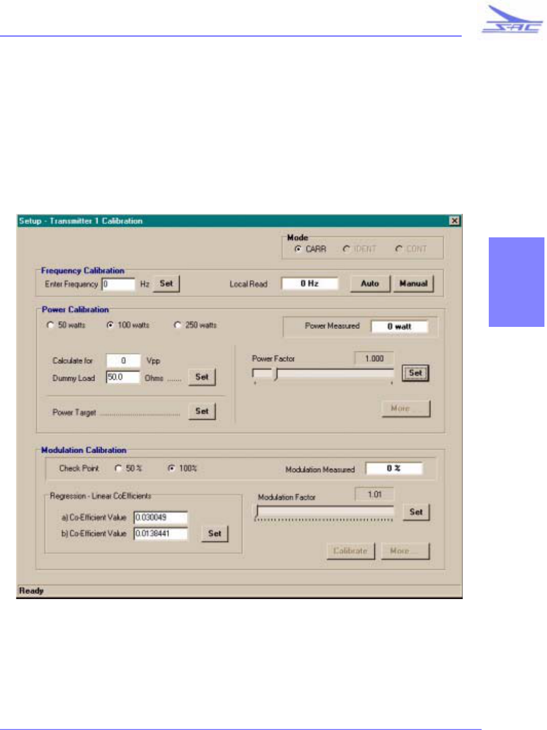
SD SERIES TRANSMITTER
93
•
•
•
•
•
•
SOUTHERN AVIONICS COMPANY
SECTION 3
Note:Normally the DDS section is extremely accurate (± 3Hz) by itself. However a correction
coefficient based on precision test equipment is generated at the factory and stored in the Controller /
Monitor boards NVRAM. This Number is used to control the DDS output and will correct the
frequency further. At the same time the on board frequency counter is also corrected to bring the test
equipment , the output and the input into agreement. The Calibration routine should only be run if a
component of the system needs replacement or if precision test equipment indicates the system is out
of tolerance.
8.4.4 Click on Setup (see section 7.3) then click on Calibration opening the Frequency / Power /
Modulation calibration window. NEED NEW WINDOW BELOW WHICH ADDS
MANUAL MODE TO MATCH PROC!!
8.4.5 Type in the frequency of operation in the window labeled "Enter Frequency"
8.4.6 Click on Monitor and wait until the reading in the Local Read window stabilizes (about 10
seconds)
8.4.7 A choice is now available as to the method of calibration. If Auto is clicked The controller /
monitor will recalibrate the output frequency based on its own internal counter which itself is
corrected at the factory. If Manual is selected the frequency as read by precision external
equipment must be input and the correction will be based on that . (we will use the latter here.)
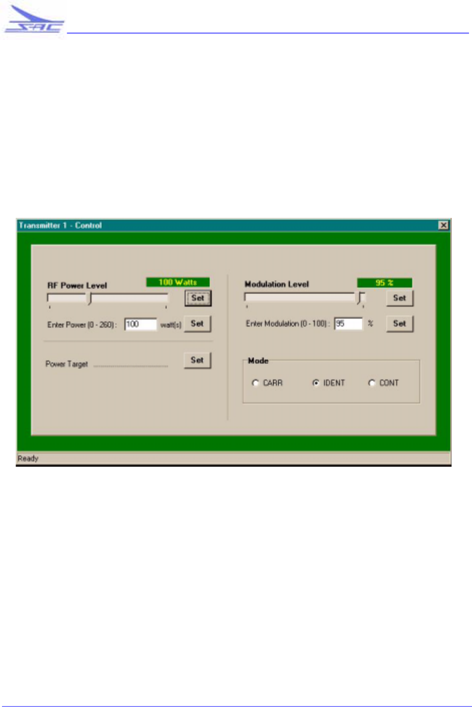
SD SERIES TRANSMITTER
94
•
•
•
•
•
•
SOUTHERN AVIONICS COMPANY
8.4.8 Click on Manual and a popup window will appear. Enter the external frequency counters
readout and click OK
8.4.9 After a few moments verify that the frequency now being read on the PC monitor agrees with
the Test equipment. This completes Frequency calibration.
8.4.10 Close the Calibration and the Setup windows
8.5 RF Power output checks
8.5.1 Scope the output of the transmitter at the Dummy Load
8.5.2 On the PC main window again click on Control and verify a popup window as follows:
8.5.3 Manually enter or adjust the slider for 10 watts RF output power.
8.5.4 Verify the power output level agrees with the PC levels with the Scope using the formula P =
(Vpp÷2.828)² / RDUMMY LOAD (a direct reading calibrated power meter is also suitable). The
tolerance is the same as a portable Bird wattmeter, 5%
8.5.5 Increase power in 5 or 10 watt steps up to the maximum allowable power verifying the power
read on the test equipment agrees with the PC readout to a 5% tolerance.
8.6 Power Calibration
8.6.1 If the Output Power is out of tolerance a power calibration will be required. Click on Setup,
then Click on Calibration
SD SERIES TRANSMITTER
95
•
•
•
•
•
•
SOUTHERN AVIONICS COMPANY
SECTION 3
WARNING ! These Calibrations are normally done at the factory using Calibrated precision test equipment
and a precision Dummy Load. A calibrated Scope and a non reactive dummy load of exact known value
must be used. The power calibration cannot be done connected to the radiating system. Any attempt to do so
will degrade system monitoring performance.
8.6.2 In the power section select a power range equal to or less than the maximum allowable
power.
8.6.3 In the Dummy Load window enter the EXACT resistance value of the dummy load
connected and click on Set.
8.6.4 The Voltage the Scope should read will show up in the Calculate For window for your
convenience.
8.6.5 Observing the Scope RF Vpp value, adjust the Power Factor slider until the scope reads the
Vpp that was calculated for it.

SD SERIES TRANSMITTER
96
•
•
•
•
•
•
SOUTHERN AVIONICS COMPANY
8.6.6 Click on Power Factor Set and Observe that the power in the Power measured window
comes into agreement with the true power as adjusted to on the scope.
8.6.7 The Power curve has now been re referenced. Exit out of the Calibration and Setup menu .
8.6.8 Click on control and perform a few spot checks to confirm that the power being read out on
the PC is accurate. Power calibration is complete. Leave the Scope attached to the dummy
load and leave the System set at full legal output power.
8.7 Modulation Checks
8.7.1 Note the carrier only Vpp level on the Scope and write it down.
8.7.2 Click on Control and enter 100% modulation either manually or with the slider.
8.7.3 Set the Scope for reading a 400 or 1020 Hz modulation envelope. Verify the modulation
envelope just touches zero baseline at modulation valleys
8.7.4 Verify that the modulation Vpp peaks are reaching twice the carrier Vpp ,earlier noted, within
5%
8.7.5 On the PC, adjust the Modulation level down to 50%
8.7.6 Read on the Scope measuring the valley and peak of the envelope. Using the formula
Mod% = (Vmax-Vmin) / (Vmax+Vmin) compute the actual modulation.
8.7.7 Verify the set modulation and the observed modulation% agree to within 5%
8.7.8 If the Modulation does not track between these two points a calibration must be performed.
8.8 Modulation Calibration
8.8.1 Refer to the SDF31002 , Page 10, drawing and locate the Analog I/O PCB (SLP10005) in the
Controller Section. Connect a Scope probe to TP102 ...(use TP0 for GND)
8.8.2 Adjust the modulation level to 100%
8.8.3 Adjust R10 on the same PCB until the waveform just touches the zero or GND reference point
at its negative most excursion.
8.8.4 Meter TP103 and adjust R101so it reads 4.0VDC
8.8.5 Meter TP104 and adjust R102 so it reads 4.0VDC
8.8.6 Remove the scope and meter connections
8.8.7 Click on Setup then click on Calibration.
SD SERIES TRANSMITTER
97
•
•
•
•
•
•
SOUTHERN AVIONICS COMPANY
SECTION 3
8.8.8 Click on the 50% set point
8.8.9 Verify that the factory Modulation Coefficients are correctly entered. These will be listed in
the factory acceptance test sheet. Re-enter them if they are corrupted or missing. Click on Set
when they are correct
8.8.10 Adjust the Modulation Factor Slider until the modulation measured window reads 50%
8.8.11 Click on the 100% setpoint
8.8.12 Verify that the modulation setting reads correctly at both points.
8.8.13 That ends modulation calibration.
8.9 Ident. Checkout

SD SERIES TRANSMITTER
98
•
•
•
•
•
•
SOUTHERN AVIONICS COMPANY
8.9.1 Close the Calibration and the Setup windows.
8.9.2 Click on Control and in the Mode section, Click on IDENT
8.9.3 Set the Modulation Level to 95% and click on Set .
8.9.4 Attach the Scope to the Dummy Load and verify that the output RF modulation envelope is
being Keyed with the proper Morse code ID and timing interval as specified by the USER
during setup.
8.10 Limits Tests.
8.10.1 On the PC, Click on Control and enter a Power level greater than the Maximum allowable
power.
8.10.2 Observe that the controller /Monitor will not allow a power greater than the systems
maximum allowable power rating as purchased.
8.10.3 Return the power setting to an allowed level.
8.10.4 Enter a modulation level above 100%
8.10.5 Observe that the Controller/Monitor will not allow more than 100% modulation.
8.10.6 Return the modulation setting to 95%
8.11 Optional DC/DC testing
8.11.1 If Battery backup operation is to be utilized to provide power during AC power line failures
Go to the Optional DC Installation Section which is included in the Options section. An OEM
battery charger modified to input charge/discharge information will be explained there.
8.12 Optional AWOS audio PCB.
8.12.1 The Audio PCB is installed and set up at the Factory and is not designed to be adjusted in the
field. The Customer input level should typically be set to -17dBm however levels up to +5
dBm are acceptable
8.12.2 Note that the AWOS modulation path is NOT controlled by the Controller /Monitor. Its own
AGC circuitry will prevent any sustained modulation in excess of the alignment value of 95%
irregardless of the customer input level
8.13 Closing up the system
8.13.1 On the PC open the control window if not already opened and set the RF Power output to Zero
8.13.2 Toggle the AC mains power switch OFF
8.13.3 Replace all the previously removed front panels except the main watertight system housing
cover.
8.13.4 Disconnect the Dummy load .
8.13.5 All general transmitter Dummy Load installation checks are complete. The transmitter is
ready to be connected to the Beacon Site antenna system and no further adjustments will be
required. It is not advisable to attempt any adjustments while connected to the Antenna
system except those allowed by software.
9.0 PLACING THE SYSTEM IN OPERATION
9.1 Connecting to a Southern Avionics Antenna Coupler

SD SERIES TRANSMITTER
99
•
•
•
•
•
•
SOUTHERN AVIONICS COMPANY
SECTION 3
9.1.1 Install the Coupler /Antenna combination according to the Coupler Installation Manual which
depends on which type is purchased.
9.1.2 Connect the furnished N terminated Coax from the Transmitter RF output N connector to the
Antenna Coupler . SAC couplers come with a standard N connector.
9.1.3 Using the PC to control the Transmitter, follow power-up and tuning directions in the coupler
manual. Basically the coupler must be set up to present a 50 OHM , minimally reactive load to
the Transmitter .
9.2 Connecting to an OEM coupler
9.2.1 Depending on the Coupler an adapter may need to be furnished or a new cable fabricated by
the USER. It is the USER's responsibility to verify that the coupler is one designed for a
standard 50 Ohm non reactive input.
The Installation Section is Complete

SD SERIES TRANSMITTER
100
•
•
•
•
•
•
SOUTHERN AVIONICS COMPANY
This page is intentionally left blank.

SD SERIES TRANSMITTER
101
•
•
•
•
•
•
SOUTHERN AVIONICS COMPANY
SECTION 4
4 MAINTENANCE
4.1 ALIGNMENT AND ADJUSTMENT
1.0 THE STANDARD ALIGNMENT CONFIGURATION
The standard alignment configuration is a way in which the SD250 is connected to power and load to ensure
reproducibility. Any subsequent alignment procedure assumes the following hook-up.
0.1 Connect AC mains L1 to user section TB1-1 (115/230 VAC Hot )
0.2 Connect AC mains L2 to user section TB1-2 (115/230 VAC Neutral or Hot
0.3 Connect AC mains GND to user section TB1-3 ( AC Power GND )
0.4 Connect the main cabinet ground to a good Earth ground.
0.5 Connect RF Out to a 50 Ohm non-reactive load.
0.6 Connect Battery I Sample to TB1-4
0.7 Connect Battery + to TB1-5
0.8 Connect Battery - to TB1-6
0.9 The Local PC used to communicate with the SD250 should be commonly grounded with the unit.
Be aware that many PC's are not shielded that well and may behave strangely or lock up if located where
intense RF fields exist. Therefore keep the PC as far away from the coupler /antenna as possible.
4.2 CONTROL MONITOR
4.2.1 ANALOG I/O ALIGNMENT
1.0 PRELIMINARY SET-UP
0.1 Successful alignment of this PCB requires a fully functional system and a previously
aligned RF section.
0.2 Adjust R14 And R15 fully CCW
0.3 Verify that all ac and dc power switches are turned off
0.4 Connect a PC to the Controller / Monitor local port with an RS232 null modem cable.
0.5 Turn the PC on and Load and Run the USER Software supplied with the System
0.6 Turn on AC main power switch
0.7 Turn on the Controller / Monitor AC Distribution power switch
0.8 Turn on the Transmitter 1 AC Distribution power switch
0.9 On the PC click on Open Port
0.10 Click on ID CONFIG and set up for the normal frequency of operation.
0.11 Click POWER ON

SD SERIES TRANSMITTER
102
•
•
•
•
•
•
SOUTHERN AVIONICS COMPANY
1.0 FORWARD / REFLECTED POWER ALIGNMENT
1.1 Set Mode to CARRIER
1.2 Set the RF POWER level to the maximum power allowed.
1.3 Meter TP101 and adjust R101 for 3.50VDC (this setting allows for continuous modulation
power readings not to exceed 5.0VDC max )
1.4 Set the RF POWER level to Zero
1.5 Disconnect the dummy load creating a 100% reflected power condition
1.6 Increase RF POWER to 25 watts
1.7 Meter TP101 and record
1.8 Meter TP102 and adjust R102 until it is the same as TP101
1.9 Set the RF POWER level to Zero
1.10 Re-connect the dummy load and connect calibrated Scope to read Power accurately
1.11 On PC click on Power Calibration
1.12 Follow screen prompts to establish the Power Correction Factor. When complete make sure
to STORE results.
1.13 Exit the Calibration Menu
1.14 Check the Power calibration from low power to high power and verify Power indicated by
the Controller/ Monitor as seen on the PC readout is accurate to within 2%
2.0 MODULATION DETECTOR ALIGNMENT
2.1 Set Mode to CONTINUOUS
2.2 Set MODULATION to 50%
2.3 Set the RF POWER level to 50% of the maximum power allowed
2.4 Connect a scope to TP1 and verify the presence of a tone frequency audio AC signal riding
above ground.
2.5 Connect the scope to TP2 again verifying the presence of the same tone frequency audio
signal being clamped near ground.
2.6 Adjust R8 until the negative swing of the signal just touches ground.
2.7 On the PC increase the RF POWER level to the Maximum Allowed or 50 Watts whichever
is greater.
2.8 Attach a meter to TP3 (Vmax DC output)
2.9 Adjust R14 until TP3 reads 4.0 VDC
2.10 Attach a Meter to TP4 (Vref DC output)
2.11 Adjust R15 until TP4 reads 4.0VDC

SD SERIES TRANSMITTER
103
•
•
•
•
•
•
SOUTHERN AVIONICS COMPANY
SECTION 4
4.2.2 DIGITAL I/O ALIGNMENT
1.0 PRELIMINARY SET-UP
1.1 Successful alignment of this PCB requires a fully functional system and a previously
aligned RF section.
1.2 Verify that all ac and dc power switches are turned off
1.3 Adjust R5 fully CW
1.4 Connect a PC to the Controller / Monitor local port with an RS232 null modem cable.
1.5 Turn the PC on and Load and Run the USER Software supplied with the System
1.6 Turn on AC main power switch
1.7 Turn on the Controller / Monitor AC Distribution power switch
1.8 Turn on the Transmitter 1 AC Distribution power switch
1.9 On the PC click on Open Port
1.10 Click on ID CONFIG and set up for the normal frequency of operation.
1.11 Click POWER ON
1.12 Set the RF POWER level to Zero
1.13 Set Mode to CARRIER
2.0 PULSE WIDTH MODULATOR ALIGNMENT
2.1 Scope TP2 and adjust R9 for a 75,000 ±500 Hz, +4 VDC to -4 VDC triangle-wave.
2.2 Scope TP3 and observe a 75000 Hz square wave that is +12Vpk and less than 50% duty
cycle.
2.3 Adjust R28 for an exact 45% duty cycle square-wave at TP3. Note that this setting is critical
and is the basis for modulation purity and all subsequent power alignment. Calibration of
the RF section is based on this waveform.
2.4 Set the RF POWER to the maximum allowed power or 100 watts whichever is LEAST
2.5 Measure the output power with a calibrated scope at the dummy load.
2.6 If the power output is not within 2% of the power setting then the output of the controller/
monitor must be verified and the calibration pot on the PA Power supply PCB must be re-
adjusted. This is easy to do. It must be stressed that tweaking of the duty cycle to achieve
alignment is not acceptable.
2.7 Set up the scope attached to the dummy load for monitoring the modulation envelope.
2.8 Set the RF POWER to 25 watts.
2.9 Set the Mode to CONTINUOUS
2.10 Set the Modulation to 100%
2.11 Adjust R30 until the modulation envelope is indicating 100% modulation
2.12 Set the RF POWER level to the maximum power allowed.

SD SERIES TRANSMITTER
104
•
•
•
•
•
•
SOUTHERN AVIONICS COMPANY
2.13 Fine Adjust R30 again for 100% modulation.
2.14 Set the RF POWER to 25 watts.
2.15 Set the Modulation to 125%
2.16 Adjust R5 until the modulation envelope peak just begins to be limited as indicated by flat-
topping.
2.17 Reduce Modulation to 95%
2.18 Set the RF Power to the normal allowed output Power
2.19 Set the Mode to IDENT
2.20 If the optional Audio PCB is included proceed to the SLP10020 alignment section
2.21 This completes Digital I/O alignment
4.2.3 AUDIO OPTION (AWOS) ALIGNMENT
PRELIMINARY SET-UP
2.1 Successful alignment of this PCB requires a fully functional system and a previously
aligned Digital I/O PCB
2.2 Verify that all ac and dc power switches are turned off
2.3 Disconnect the main AC input by either unplugging the unit from the mains or turning OFF
the main USER supply breaker.
2.4 An audio test generator with a 600 Ohm variable output calibrated from +10 to -40 dbm is
required.
2.5 Connect the Audio Generator output to TB6 on the User Interface PCB in the USER
section. Connect the individual wires as follows: (see assembly drawing SAP10006)
+Audio to TB6-1
- Audio to TB6-2
Shield to TB6-3
2.6 Remove the Digital I/O PCB from the Control Monitor Section and set JP1 to 1-3 and JP2
to 1-2 . Install the piggyback Audio PCB (see drawing SAP10020 for details)
2.7 Set The Audio PCB Jumpers JP1 to 1-3, JP2 to 1-2
2.8 Place the Digital I/O PCB on an extender and re-install it.
2.9 Re-establish the main AC Power source.
2.10 Connect a PC to the Controller / Monitor local port with an RS232 null modem cable.
2.11 Turn the PC on and Load and Run the USER Software supplied with the System
2.12 Turn on AC main power switch
2.13 Turn on the Controller / Monitor AC Distribution power switch
2.14 Turn the Transmitter 1 AC Distribution power switch ON
2.15 On the PC click on Open Port
2.16 Click on ID CONFIG and set up for the normal frequency of operation.

SD SERIES TRANSMITTER
105
•
•
•
•
•
•
SOUTHERN AVIONICS COMPANY
SECTION 4
2.17 Click POWER ON
2.18 Set the RF POWER level to Zero
2.19 Set the Modulation to 95%
3.0 AUDIO AMPLIFIER COMMON MODE BALANCE
3.1 Set the Audio generator to output 1000Hz @ 0.0 dBm
3.2 Scope TP1 and adjust R22 for minimum signal @ 1000Hz. This should be less than 20
millivolts.
3.3 Turn the Controller / Monitor AC Distribution power switch OFF
3.4 On the Audio PCB move the jumpers JP1 to 1-2 and JP2 to 1-2
4.0 AUTOMATIC GAIN CONTROL
4.1 Connect a calibrated Modulation monitor to the transmitters output RF line
4.2 Turn the Controller / Monitor AC Distribution power switch ON
4.3 Click POWER ON
4.4 Set the RF POWER level to 25 Watts
4.5 Set the Mode to CARRIER
4.6 Set the Signal Generator to output 1000Hz @ -28Dbm
4.7 Scope TP3 and adjust R24 until it just switches to +12V(high)
4.8 Increase The Signal generator output to -17 dBm
4.9 Temporarily adjust R29 until 95% modulation is read on the Modulation monitor
4.10 Verify AGC capture takes place indicated by no further increase in Modulation percentage
as the signal generators output is increased up to +10dBm.
4.11 Set the Audio Generator to -17dBm
4.12 Adjust R29 for Zero modulation.
4.13 On the PC switch the Mode to CONTINUOUS
4.14 Adjust R2 until the Monitor reads 20% modulation
4.15 Reduce the Audio Generator output to -30 dBm
4.16 Verify the Keyer Tone modulation level returns to 95% within 5 seconds
4.17 Increase the Audio Generator output to +10 dBm
4.18 Adjust R29 until the composite modulation reads 95%. If only a scope is available, adjust
the modulation valleys to just touch the zero (gnd) baseline and then back off the adjustment
1/2 turn.
4.19 On the PC click on Power off.
4.20 Turn All Power switches OFF
4.21 Replace the Digital I/O PCB in its Slot
4.22 Audio PCB alignment is Complete.

SD SERIES TRANSMITTER
106
•
•
•
•
•
•
SOUTHERN AVIONICS COMPANY
4.3 TRANSMITTER
4.3.1 PA POWER SUPPLY ALIGNMENT (PAPS)
Safety Note: Dangerous voltages are present on this PCB during power on tests. Be very careful when working on
this board. When power is removed dangerous voltage will still be present on the HV cap bank. A built in HV
Bleeder on the mother board will discharge the HV cap bank in about 30 seconds. Red LED DS1 will be on if power
is present. Another LED on the mother board will also indicate HV presence. Verify this with a meter check at either
end of R69 until you are personally confident the bleeder circuit and associated indicators are operating correctly.
Note: To be able to successfully complete this alignment without using special loading fixtures we rely on a normal
load being presented to the supply by the RF Power Amplifier PCB and Filter PCB. Therefore it is important that
those PCBs be aligned and in good working order.
1.0 PRELIMINARY CHECKS AND ADJUSTMENTS
1.1 Verify that all ac and dc power switches are turned off .
1.2 Connect a PC to the Controller / Monitor local port with an RS232 null modem cable.
1.3 Turn the PC on and Load and Run the Controller / Monitor user Software supplied with the System
1.4 Remove the RF power amplifier PCB which removes the load from the PAPS
1.5 Remove the PAPS PCB and place it on the extender fixture.
1.6 Adjust R32,R38,R15, R41, R43, R48 and R66 fully clockwise (CW)
1.7 Adjust R4, R7, and R40 fully counterclockwise (CCW)
1.8 Adjust R45 and R46 for middle range
1.9 Toggle the Manual HV switch S3 to the OFF position (actuator thrown toward the front of the PCB)
1.10 Move jumper JP1 to 3-4 (lower position) enabling local power control
2.0 DC CONTROLLER SECTION LOW VOLTAGE ALIGNMENT
2.1 Turn the main power AC switch on. . Caution! Input HV is on!
2.2 Turn the AC distribution switch for Transmitter 1 or Transmitter 2 on depending on where the extender is
being used.
2.3 Verify the presence of +50vdc on TP1 of the RF motherboard in use.
2.4 Adjust R43 for 12.00 ±0.1 vdc at TP11
2.5 Adjust R48 for 12.00 ±0.1vdc at TP13
2.6 Press the manual reset buttons S1 and S2
2.7 Adjust r4 for 4.00 ±0.01vdc at TP1
2.8 Initially adjust R7 for approximately 2.7vdc at TP5
2.9 Scope TP2 and further adjust R7 until an approximate 50% duty cycle 75khz square-wave is seen. A loose
feel to the adjustment is normal since HV feedback which stabilizes the signal is not yet present.
2.10 Read TP2 with a calibrated frequency counter and adjust R20 for 75 kHz ±500 Hz. Note that this
frequency is not critical but is optimum for the inductor used in the buck converter.

SD SERIES TRANSMITTER
107
•
•
•
•
•
•
SOUTHERN AVIONICS COMPANY
SECTION 4
2.11 Connect channel 2 of the scope to TP3 and verify that the two signals are 180 degrees out of phase and
have approximately 250 nano-seconds dead time between them. Dead time is here defined as that period
when both signals are low at the transition point between one being high and the other being low.
2.12 Connect scope channel 1 and 2 to the gates of Q1 and Q2 and verify the 75khz signals are 180 degrees out
of phase.
2.13 Important! Adjust R7 fully CCW
3.0 DC-DC CONVERTER LOW VOLTAGE ALIGNMENT
3.1 Scope TP12 and adjust R45 for 75kHz ±500Hz . Then adjust R46 for 50% duty cycle.
3.2 Scope The Gates of Q4 and Q5 and readjust R46 until the 75 kHz signal is at a 50% duty cycle. Some
readjustment between R45 and R46 may be necessary.
3.3 Remove the scope leads
3.4 Adjust R57 until TP16 is at 2.50 ±0.01VDC . This sets the DC-DC HV shut down level to 250V or more.
Built in hysteresis will cause the supply to slowly discharge to 220VDC and again turn on if no current is
being drawn by the RF Power Amplifier.
3.5 Meter TP14 and adjust R66 for 3.75 ±.01 VDC This sets the DC-DC over-current shut down point
equivalent to 250W @125% Modulation. This setting is good for all power ranges.
4.0 DC CONTROLLER HV ALIGNMENT , UNLOADED
4.1 Adjust R82 for 1.30 volts at TP17. This sets the inrush limiter to drop out at 130 Volts
4.2 Using the manual HV switch S3 turn on High Voltage. Be Aware of any unusual behavior and be ready to
shut off main power.
4.3 Relay K1 will be heard activating immediately followed by K2 a short time later. This is the inrush
sequence. The first time HV is turned on, two (2) distinct relay closures should be heard as the HV caps
charge up. If the Cap bank is already charged both relays will pull in simultaneously. Verify that DS1
illuminates as well as the LED on the mother board.
Note: It is important to realize that the HV ON/OFF switch does not bleed off the HV cap bank. The bleeder turns on
only when 50V turns off. This means AC and DC power must both be removed.
4.4 Verify 250VDC at TP2 on the RF Motherboard.
4.5 Meter TP6 And slowly Adjust R7 (power output calibration control) observing the voltage gradually
increasing.
4.6 Depending on the maximum power the transmitter will be operating at continue to adjust R7 until the
nominal output DC voltage for that power is reached as listed below:

SD SERIES TRANSMITTER
108
•
•
•
•
•
•
SOUTHERN AVIONICS COMPANY
4.7 The PAPS is now calibrated for Maximum normal output based on an expected 4.0V feed from Controller
/ Monitor. Do not disturb the R7 setting again until it is connected to the RF Amplifier it will feed, at
which time fine adjustments may be required.
4.8 Adjust R4 (manual power control) fully CCW. In the future any manual test power control will be done
with this pot only.
4.9 Meter TP8 and Adjust R32 to read 1.90 ±0.05 VDC setting the DC Controller over-voltage fault level to
190VDC
4.10 Meter TP9 and adjust R38 to read 0.59V. This sets the Maximum peak current to a value similar to that
drawn when running 250 Watts and over-modulating 120% ( This setting should be set slightly higher
than the RF PA shutdown setting allowing better diagnostic analysis)
4.11 Turn off all power switches
4.12 Switch OFF HV manual control switch S3
4. 1 3 A ll o w a n y H V t o Bl e ed off e ns u ri ng H V i nd i ca to r LE D DS 1 i s ex ti n gu is h ed .
5.0 DC CONTROLLER HV ALIGNMENT WITH RF POWER AMPLIFIER INSTALLED
5.1 Move JP1 the jumper to 1-2 (the upper position) enabling Controller / Monitor control
5.2 Install The RF Power Amplifier PCB
5.3 Ensure that the Filter/Bridge PCB is installed and strapped for the Frequency of operation
5.4 On the RF Mother PCB remove F1 and connect a 10 Amp Current meter across the fuse-holder.
5.5 Connect Channel 1 of the Scope across the 50 Ohm NI dummy load.
5.6 Turn on Main AC power and switch on Controller / Monitor power
5.7 On PC click on the ID CONFIG button and set the frequency of operation for the filter installed. Close the
window when done.
5.8 Turn on Transmitter 1 AC power distribution switch .
5.9 On the PC Click on the POWER ON button and verify the HV led illuminates.
5.10 On the PC click on the CONTROL button opening the Power/Modulation control window
5.11 Set the RF power level to the 25% of the maximum power allowed on site. Verify the correct RF power
output on the Scope. Pout = (RFVPP ÷ 2.828)² ÷ R dummy load
5.12 Increase Carrier power until maximum allowed power is reached as indicated on the monitoring Scope on
the dummy load.
Maximum Power DC Controller Output
250 Watts 160 VDC
100 Watts 100 VDC
50 Watts 72 VDC
25 Watts 50 VDC

SD SERIES TRANSMITTER
109
•
•
•
•
•
•
SOUTHERN AVIONICS COMPANY
SECTION 4
5.13 Set the modulation level to 100%
5.14 Meter TP10 Set R41 fully CW and adjust R40 until the voltage equals the current in Amps on the current
meter.. ( Example: 2.7 amps = 2.7volts at TP10 )
5.15 In the PC control window, set the RF Carrier power to Zero.
5.16 Turn the DC Input power switch on.
5.17 In the PC control Window again adjust RF Carrier Power output to Maximum allowed output as read by
the scope.
5.18 Turn OFF the Transmitter AC power distribution switch and verify that Controller / Monitor automatically
folds-back the RF Power to 80% of Maximum allowed output. This fold-back feature helps preserve
battery life in an emergency situation.
5.19 Turn Transmitter AC Distribution Switch back on and verify Full legal power levels are re-established.
5.20 Turn the DC input supply switch OFF
5.21 On the PC Control Panel window, set RF output and Modulation % to Zero
5.22 Close the control Window on the PC and Click on Power OFF, at which time HV relay drop-out should be
heard
5.23 Click on the CLOSE PORT button
6.0 PA POWER SUPPLY ALIGNMENT IS COMPLETE
6.1 Turn the Transmitter's AC Power off and allow HV to discharge
6.2 Turn Controller / Monitor's AC power OFF
6.3 Remove the PA Power Supply from the extender fixture.
6.4 Disconnect the Current meter connected to F1 fuse holder on the RF Mother Board and replace F1
6.5 Re-install the PA Power supply in the RF Module.
4.3.2 RF POWER AMPLIFIER ALIGNMENT (PA)
Safety Note: Dangerous voltages are present on this PCB during power on tests. Be very careful when working on
this board. When power is removed dangerous voltage will still be present on the HV cap bank. A built in HV
Bleeder on the mother board will discharge the HV cap bank in about 30 seconds. On The PA Power supply PCB Red
LED DS1 will be on if power is present. Another LED on the mother board will also indicate HV presence. Verify

SD SERIES TRANSMITTER
110
•
•
•
•
•
•
SOUTHERN AVIONICS COMPANY
this with a meter check at either end of R69 until you are personally confident the bleeder circuit and associated
indicators are operating correctly.
Note: To be able to successfully complete this alignment without using special loading fixtures we rely on a normal
load being presented to the RF Power Amplifier by the Filter/Bridge PCB. Therefore it is important that the Filter/
Bridge PCB be optioned for the correct frequency and in good working order.
1.0 PRELIMINARY SET-UP
1.1 Verify that all ac and dc power switches are turned off
1.2 Connect a PC to the Controller / Monitor local port with an RS232 null modem cable.
1.3 Turn the PC on and Load and Run the Controller / Monitor user Software supplied with the System
1.4 Remove the RF Amplifier PCB and place it on the extender fixture.
1.5 Set JP1 jumper to connect 1-2
1.6 Adjust R38 fully CCW
1.7 Adjust R14,R20, and R28 fully CW
1.8 Turn The Main AC power switch ON
1.9 Turn the Controller / Monitor AC distribution switch ON
1.10 On the PC screen Click on OPEN PORT
1.11 Click on ID CONFIG and set up for the proper Site RF frequency and Tone
1.12 Click on Power OFF
2.0 RF Power Amplifier low level alignment
2.1 Turn the Transmitter (1 or 2) AC Power Distribution Switch ON
2.2 Meter TP1and Adjust R38 CW to read 12.0 ± 0.01 vdc
2.3 ON the PC click on Power ON
2.4 Scope TP10 and verify the presence of 5V square-wave RF at the previously selected Frequency. If
an outside user source of RF is being used it should have a minimum level of 1Vpp
2.5 Scope TP9 and adjust R31 for a 10 Vpp RF signal at the same frequency
2.6 Scope TP11 and adjust R37 for a 50% duty-cycle
2.7 Scope TP12 and verify a 50% duty cycle 30Vpp RF signal at the same frequency
2.8 Using 2 channels Scope the Phase of the Gate signals at Q4,5,6 and 7.
2.9 Verify that Q4 and Q7 are in phase.
2.10 Verify that Q5 and Q6 are in phase
2.11 Verify that Q4 and Q5 are 180 deg. Out of phase
2.12 Attach the Dual Scope probes to TP2 and TP3
2.13 Verify TP2 is a +12Vpk 75kHz square-wave with a 45% duty cycle
2.14 Verify TP3 is a +12Vpk 75Khz square wave 180 degrees out of phase with TP2

SD SERIES TRANSMITTER
111
•
•
•
•
•
•
SOUTHERN AVIONICS COMPANY
SECTION 4
2.15 Be sure of the above Verification! TP2 and TP3 must be correct and out of phase or serious damage
to the PA will result when HV is applied in the subsequent steps.
2.16 Turn Transmitter (1 or 2) AC Power Distribution switch OFF
3.0 RF Power Amplifier high level adjustments.
3.1 Connect an RF Ammeter in series at JP1 the large current jumper.
3.2 Turn Transmitter (1 or 2) AC Power Distribution switch ON
3.3 On the PC click on POWER ON.
3.4 On the PC, click on Control opening the Power/Modulation page
3.5 In the PC Control window Set the mode to CARRIER
3.6 Set the RF power control to 10 watts and click on set.
3.7 Scope the RF output at the dummy-load and verify the power output is 10 ± 0.5 Watts. Also verify
the waveform is a clean sinewave.
3.8 On the PC increase the RF power output, being careful not to exceed the test meter rating, to the
maximum allowable output and verify it at the dummy load. If this power is too much for the meter
range select the highest power you can read on scale
3.9 Read the current displayed on the RF Ammeter. (@100W 2.7Amps is typical) ,divide the Ammeter
value by two (2) and record the value.
3.10 Connect a Meter between TP4 and TP8 then fine Adjust the duty cycle with R37 until the meter reads
Zero volts
3.11 Adjust R14 until TP4 reads the recorded value
3.12 Adjust R28 until TP8 reads the recorded value
3.13 Check The PC and verify that the Controller / Monitor PAI 1 & 2 current readings agree with the
values set at TP4 and TP8
3.14 On the PC set the RF power control to Zero 0 watts and click on set.
3.15 On the PC click on POWER OFF
3.16 Turn Transmitter (1 or 2) AC Power Distribution switch OFF
3.17 Disconnect the Ammeter and Reinstall the JP1 jumper.
3.18 Remove the RF Power Amplifier from the extender fixture and re-install it in the RF section.
3.19 Turn Transmitter (1 or 2) AC Power Distribution switch ON
3.20 On the PC click on POWER ON
3.21 Meter TP7 and on the PC set the RF power for 5 watts.
3.22 Scope the output to the Dummy load and verify The power output is correct ± 5%
3.23 Verify the PAV being reported by the Controller / Monitor agrees with the TP7 reading
3.24 Continue checking the power accuracy across the allowed power range in 5 watt intervals to 50 watts
, 10 watt intervals to 250 watts. Check that Controller / Monitor PAV readings agree with TP7
3.25 On the PC set the RF power control to the maximum allowable output and click on set.

SD SERIES TRANSMITTER
112
•
•
•
•
•
•
SOUTHERN AVIONICS COMPANY
3.26 On the PC set Mode to Continuous
3.27 On the PC set and increase modulation in steps from 10 to 100% verifying a proper sinusoidal
modulation envelope.
3.28 With Modulation at 100%, scope the output at the Dummy load and adjust R20 CCW until the
shutdown occurs. the Controller / Monitor should indicate a fault condition.
3.29 Back off R20 and reset the fault on the PC. Verify Modulated output returns.
3.30 Increase Modulation to 120% and adjust R20 CCW again slowly until a shutdown occurs.
3.31 On the PC adjust the Modulation to 95%, then set the Mode to IDENT.
3.32 Monitor the output for one minute and verify no faults occur
3.33 The RF Power Amplifier Alignment is complete
4.3.3 FILTER / BRIDGE ALIGNMENT (FB)
Safety Note: Dangerous RF voltages are present on this PCB during power on tests. Be very careful when working
on this board.
1.0 PRELIMINARY SET-UP
1.1 Verify that all ac and dc power switches are turned off
1.2 Connect a PC to the Controller / Monitor local port with an RS232 null modem cable.
1.3 Turn the PC on and Load and Run the Controller / Monitor USER Software supplied with the
System
1.4 Remove the Filter/Bridge PCB from the RF Section and place it on an extender fixture
1.5 Adjust R7 and R11 fully CW
1.6 Set jumper JP13 and JP14 to B
1.7 Set jumpers JP1 thru JP12 according to the Frequency Band Chart on the Filter/Bridge Schematic
(SEP10002 / 0x ) sheet 1 of 3.
2.0 POWER BRIDGE BALANCE
2.1 Turn The Main AC power switch ON
2.2 Turn the Controller / Monitor AC distribution switch ON
2.3 Turn the Transmitter (1 or 2) AC distribution switch ON
2.4 On the PC screen Click on OPEN PORT
2.5 Click on ID CONFIG and set up for the proper Site RF frequency and Tone
2.6 Click on Power ON and observe the HV lamp on the PAPS comes on
2.7 Click on Control and when the window opens select CARRIER MODE
2.8 Set the Carrier Power level to 25 watts

SD SERIES TRANSMITTER
113
•
•
•
•
•
•
SOUTHERN AVIONICS COMPANY
SECTION 4
2.9 Meter TP1 and adjust R21 for a minimum reading . This reading should be close to zero volts.
2.10 On the PC click on Power OFF
2.11 Turn the Transmitter (1 or 2) AC distribution switch OFF. Wait as the HV lamp slowly extinguishs
2.12 Set Jumper JP13 and JP14 to A
2.13 Turn the Transmitter (1 or 2) AC distribution switch ON
2.14 Click on Power ON and observe the HV lamp on the PAPS comes on
2.15 Again, set the Carrier Power level to 25 watts
2.16 Meter TP2 and adjust R22 for a minimum reading . This reading should typically be approximately
0.160VDC.
2.17 Meter TP1. The reading should typically be approximately 2.0vdc
2.18 The Bridge is now balanced. Leave all jumpers where they are and continue with the procedure.
3.0 FAULT SET-UP
Note:Forward and reflected power can also used to trigger fast fault interrupts rather than the slower
routine monitoring the controller / monitor accomplishes. It is up to the USER how these should best be set
up but the following default settings are factory standard.
3.1 The fault lamp on the Digital I/O PCB (DS3) must be monitored for the following steps. If an
optional OP-Panel is installed it must be removed to observe this lamp.
3.2 On the PC set the power to Zero RF Output and temporarily disconnect the Dummy Load
3.3 Slowly increase the RF power output until the Controller / Monitor reports 20% of the Maximum
Allowed Level as reflected power.
3.4 Adjust R11 until the Digital I/O fault LED-DS3 just illuminates.
3.5 RF output should immediately turn off.
3.6 Back off R11 and On the PC click on reset (this can also be done manually on the Filter/Bridge PCB)
and observe the Digital I/O fault LED DS3 extinguishes and RF power comes back on.
3.7 Again very slowly adjust R11 until the fault just triggers and Digital I/O fault LED-DS3 comes on.
3.8 Decrease Power output and click on reset. Increase the power again to 20% of the Maximum
Allowed Level, verifying a fault trigger occurs at that level. Re-adjust R11 if necessary .
3.9 On the PC set the RF Power to Zero
3.10 Re-attach the Dummy Load
3.11 On the PC set the RF Output to the Maximum Allowed Level. Click on CONTINUOUS tone output.
3.12 Set the Modulation to 115 %
3.13 Adjust R7 until the Digital I/O fault LED-DS3 illuminates.
3.14 Verify that RF Power output ceased immediately .
3.15 Back off R7 , reset the fault and repeat the adjustment slowly to obtain an accurate trigger point
3.16 On the PC set the Mode to IDENT, the Modulation to 95%
3.17 Click on Power OFF and turn the Transmitter (1 or 2) AC power OFF

SD SERIES TRANSMITTER
114
•
•
•
•
•
•
SOUTHERN AVIONICS COMPANY
3.18 Remove the PCB from the extender and re-install it in the RF Section
3.19 Turn the Transmitter (1 or 2) AC power ON
3.20 Click on Power ON.
3.21 Monitor the System for 2 minutes and verify no faults or shutdowns occur.
3.22 Filter /Bridge Alignment is complete.

SD SERIES TRANSMITTER
115
•
•
•
•
•
•
SOUTHERN AVIONICS COMPANY
SECTION 5
5 ANTENNAS:
The range of a beacon and antenna depends on many variables and cannot be guaranteed. The
field strength can be calculated if the ground conductivity is known, but the field strength needed
depends on the background environmental noise which depends on location. A field strength of
70V/m is generally adequate in the United States and Europe but may not be sufficient in latitudes
between 30N and 30S. Range figures given in the following sections are based on average ground
conductivity and a field strength of 70V/m.
The resistance of the antenna is dependent on many conditions over which the manufacturer has
no control. The ground condition, for example, is extremely important. In a high conductivity
ground region, the resistance will be fairly low. This is especially true on offshore oil rigs where
the ground system consists of a large metal structure over salt water. On the other hand, if the
ground conductivity is low, the resistance can become quite large. For example, permafrost in
Alaska generally makes a very poor ground and in most cases a special counterpoise system must
be used. Without a special counterpoise system, the antenna resistance may be as high as 50
ohms and the antenna efficiency will be very low.
THE MAST ANTENNA, "H" ANTENNA, AND 50-FOOT GUYED MAST ANTENNA ARE
HIGH Q, NARROW BANDWIDTH ANTENNAS. THEY SHOULD NOT BE USED FOR
VOICE MODULATION. THE SYMMETRICAL "T" ANTENNA IS THE ONLY ANTENNA
RECOMMENDED FOR VOICE MODUATION.
5.1 Mast Antenna
The Mast Antenna is a short vertical monopole with capacitive top loading and inductive center
loading. It was designed for use where space is severely limited such as on offshore structures. It
is centerloaded to be resonant at approximately 500 KHz for operation between l90 and 415 KHz
and at approximately 900 KHz for operation between 415 and 625 KHz. Tuning below the reso-
nant frequency is accomplished with the antenna coupler. There are two versions of this antenna;
one designed to be mounted on land, the other on drilling platforms or ships. Neither antenna
requires guying. A capacitive hat at the top of the 34-foot Mast Antenna consists of six 8-foot
radials. These can be shortened if necessary for clearance on drilling platforms. The counter-
poise system used for land installations consists of sixteen 60-foot radials made of #10 copper
wire with 6-foot ground rods at each end and one in the center. The offshore version of the Mast
Antenna uses the platform structure and the water for the ground system.
The range with the Mast Antenna and this transmitter depends on ground condition, frequency,
the ADF, and atmospheric noise which in turn depends on location and time. Range for most
locations in the United States with one of the lower priced ADF's is from 50 to 70 miles for fre-
quencies above 250 KHz except over low conductivity ground. SAC does not recommend this

SD SERIES TRANSMITTER
116
•
•
•
•
•
•
SOUTHERN AVIONICS COMPANY
antenna for land installations at frequencies below 250 KHz. The "T" Antenna is far superior at
all frequencies and should be used whenever space permits. The 50-foot Guyed Mast is recom-
mended for land installations where the "T" cannot be used. Calculated range over sea water with
the Mast Antenna and this transmitter is 40 miles at 200 KHz, increasing to 100 miles at 400 KHz.
Ideally, this antenna should be in a clear area; however, this is very seldom feasible on offshore
structures. Large obstacles close to the antenna will affect the directional properties and the tun-
ing of the antenna. If possible, the antenna should be installed with a clear area in the direction of
the most traffic.
The Mast Antenna is electrically very similar to a 200 pF capacitor in series with a small resistor.
See the figure at the end of this section for a plot of the capacitive reactance.
5.2 "H" Antenna
The "H" Antenna is used on the helipad of offshore structures where there is no clear area to
install the Mast Antenna. It is a wire structure that is installed on the perimeter of the helipad.
The transmitter is mounted directly beneath it so that the vertical portion of the antenna is the off-
shore structure itself. Electrical characteristics vary, depending mostly on the size of the helipad
but are generally similar to the Mast Antenna. Range is also comparable with the Mast in most
cases.
5.3 50-Foot Guyed Mast Antenna
This antenna is a guyed vertical monopole with capacitive top loading that was designed for land
installations where space is limited. The capacitive top hat consists of six 8-foot radials. The
counterpoise system consists of sixteen 60-foot radials made of #10 copper wire with 6-foot
ground rods at each end and one in the center. The antenna is guyed at the top and center.
The calculated range with the Guyed Mast Antenna exceeds the Mast Antenna but is less than the
"T" Antenna under the same conditions. This antenna is recommended for land installation where
space does not permit use of the "T" Antenna.
The Guyed Mast Antenna is electrically very similar to a 300 pF capacitor in series with a small
resistor. See the figure at the end of this section for a plot of the capacitive reactance.
5.4 Symmetrical "T" Antenna
The Symmetrical "T" Antenna is recommended if sufficient land is available. This antenna
requires a plot of ground approximately 150 feet by 350 feet.
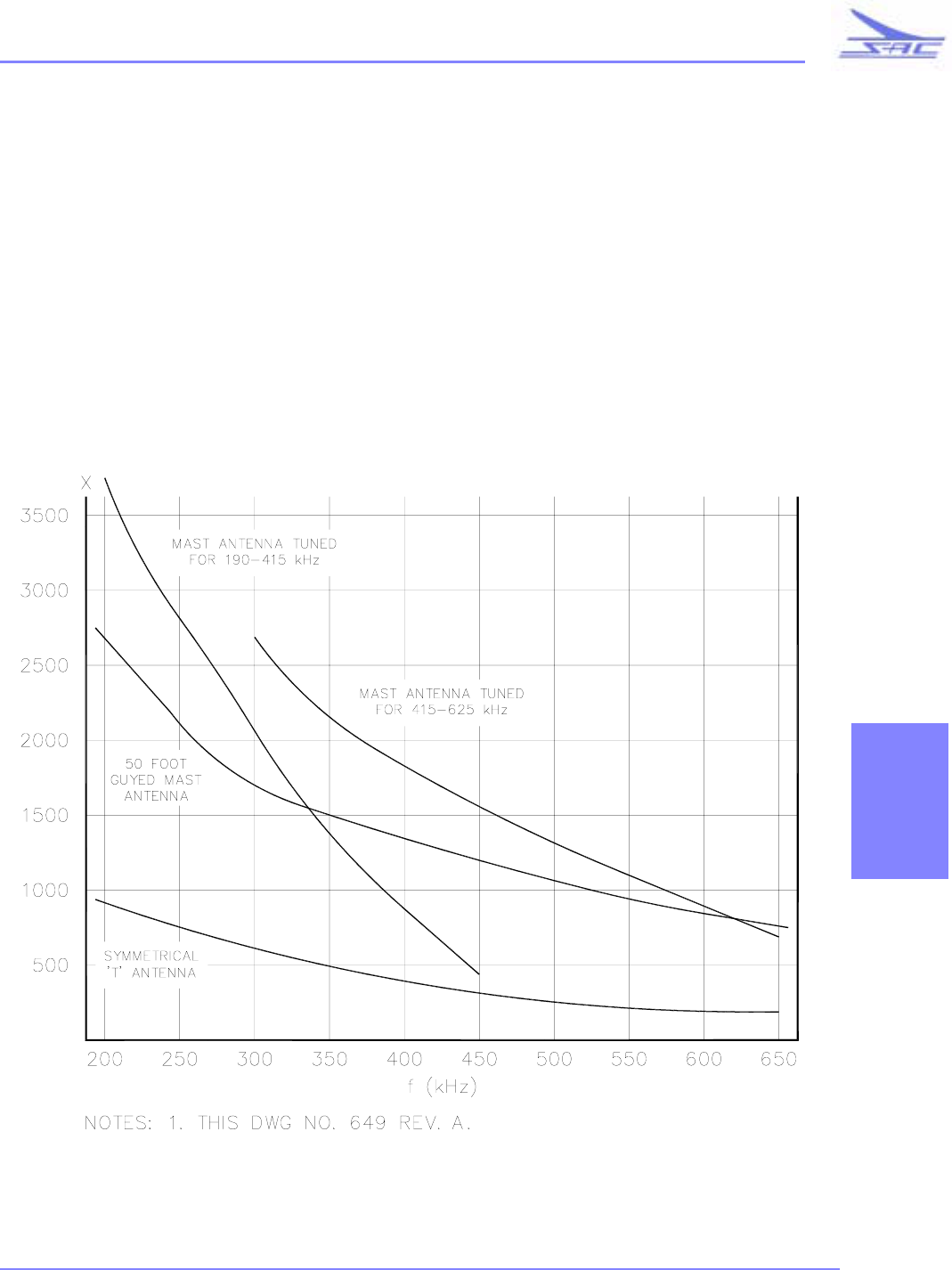
SD SERIES TRANSMITTER
117
•
•
•
•
•
•
SOUTHERN AVIONICS COMPANY
SECTION 5
The calculated range with the "T" Antenna and this transmitter for most locations in the United
States and with one of the lower priced ADF's is from 80 to 100 miles except over low conductiv-
ity ground.
These range figures are for the standard "T" Antenna with a height of 55 to 60 feet. A long range
"T" Antenna with a height of 80 to 85 feet has a range of 100 to 120 miles. If even more range is
desired, SAC can supply "T" Antennas with heights up to 200 feet.
The standard "T" is electrically very similar to a 1000 pF capacitor in series with a small resistor.
See the fiqure at the end of this section for a plot of the capacitive reactance.
649 - DIAGRAM, ANTENNA REACTANCE

SD SERIES TRANSMITTER
118
•
•
•
•
•
•
SOUTHERN AVIONICS COMPANY
6 PARTS LISTS
SLF31002/00 - ASSY, TRANSMITTER, SD SERIES DUAL (BASIC)
REFERENCE
DESIGNATOR COMPONENT DESCRIPTION
01 SLE10031 ASSY, FINAL TRANSMITTER DUAL (COLDFIRE)
1A1A3 SLP10003 ASSY, PCB, PA POWER SUPPLY
1A1A4 SLP10001 ASSY, PCB, RF POWER AMPLIFIER
4A1A3 SLP10003 ASSY, PCB, PA POWER SUPPLY
4A1A4 SLP10001 ASSY, PCB, RF POWER AMPLIFIER
5A1A3 SLP10007 ASSY, PCB, CF CONTROLLER
5A1A4 SLP10005 ASSY, ANALOG I/O AND AUDIO
5A1A5 SLP10009 ASSY, PCB, DIGITAL I/O AND PWM
5A1A6 SLP10009 ASSY, PCB, DIGITAL I/O AND PWM
5A1A7 SLP10005 ASSY, ANALOG I/O AND AUDIO
5A1A8 SLP10007 ASSY, PCB, CF CONTROLLER
5A2 SLE10004 ASSY, LOAD CENTER (COLDFIRE)

SD SERIES TRANSMITTER
119
•
•
•
•
•
•
SOUTHERN AVIONICS COMPANY
SECTION 6
SLE10004 - ASSY, LOAD CENTER (SD SERIES)
REFERENCE
DESIGNATOR COMPONENT DESCRIPTION
A1 SLP10006 ASSY, PCB USER INTERFACE
CB1 9C350021 CIRCUIT BREAKER, 1 POLE, 227 VAC / 65 VDC, 15
AMP
CB2 9C350019 CIRCUIT BREAKER, 2 POLE, 277 VAC, 50/60 HZ,
10.0 AMP
FL1 9F345000 FLTR LINE 2STG 3A FASTON
FL2 9F345001 FLTR LINE 2STG 10A FASTON
FL3 9F345001 FLTR LINE 2STG 10A FASTON
FL4 9F345001 FLTR LINE 2STG 10A FASTON
J1 9R180001 RCPT 110V
S1 9S900005 SWITCH, DPST
S2 9S900005 SWITCH, DPST
S3 9S900005 SWITCH, DPST
TB1 50000011 CONN, BARRIER TERM BLK, 8POS, 142 SERIES

SD SERIES TRANSMITTER
120
•
•
•
•
•
•
SOUTHERN AVIONICS COMPANY
SLE10031 - ASSY, FINAL TRANSMITTER DUAL (SD SERIES)
REFERENCE
DESIGNATOR COMPONENT DESCRIPTION
01 SLM10001 ASSY, TRANSMITTER ENCLOSURE (COLDFIRE)
1A1 SLE10033 ASSY, TRANSMITTER (6U) COLDFIRE
4A1 SLE10033 ASSY, TRANSMITTER (6U) COLDFIRE
5A1 SLE10032 ASSY, CONTROL MONITOR DUAL (3U),
(COLDFIRE)
J68 56000004 CONN, COAX, PANEL MOUNT, RECPT

SD SERIES TRANSMITTER
121
•
•
•
•
•
•
SOUTHERN AVIONICS COMPANY
SECTION 6
SLM10001 - ASSY, TRANSMITTER ENCLOSURE (SD SERIES)
REFERENCE
DESIGNATOR COMPONENT DESCRIPTION
15 4A000000 TERM COPPER "D" 14 AWG SOLID, 4 AWG STRD
18 9F580002 WEATHER STRIP, 1/4THK X 5/8W, BLACK FOAM
19 9R360001 RIVET 3/16" DIA. 1/4"-3/8" GRIP POP CLOSED SS

SD SERIES TRANSMITTER
122
•
•
•
•
•
•
SOUTHERN AVIONICS COMPANY
SLM10005 - ASSY, CONTROL MONITOR PANEL WITH APPLIQUE
REFERENCE
DESIGNATOR COMPONENT DESCRIPTION
A1 SLP10016 ASSY, CONTROL MONITOR PCB (COLD FIRE)
XJ1 9J021001 MOUNTING HARDWARE, D-SUB .81 LGTH 4-40
JACK SCREW KIT

SD SERIES TRANSMITTER
123
•
•
•
•
•
•
SOUTHERN AVIONICS COMPANY
This page is intentionally left blank.