Spot STAMP DTS Developer Board User Manual Stamp User s Manual
Spot LLC DTS Developer Board Stamp User s Manual
Spot >
User Manual
Axonn LLC Stamp User’s Guide-Document #9100-0160-01 Ver 1.0 1/7
Part Number 9100-0160-01
Revision 1.0
Date: October 4, 2006
2.4 GHz Stamp User’s Manual

Axonn LLC Stamp User’s Guide-Document #9100-0160-01 Ver 1.0 2/7
Table of Contents
1. 2.4 GHz Stamp Product Description…………………………………………
2. Typical Integration……………………………………………………………
3. Product Specifications………………………………………………………...
3.1 Specifications………………………………………………………………
3.2 Pin Diagram………………………………………………………………..
3.3 Pin Descriptions…………………………………………………………….
4. Air Interface…………………………………………………………………....
4.1 Frequency…………………………………………………………………....
4.2 Power……………………………………………………………………….
4.3 Timing………………………………………………………………………
5. Serial User Interface………………………………………………………….
5.1 Message Protocol…………………………………………………………...
5.2 Tips………………………………………………………….........................
5.3 Timing………………………………………………………….....................
5.4 Digital I/O…………………………………………………………..............
6. Mounting Guidelines………………………………………………………….
7. Power Supply Requirements………………………………………………….
8. Environmental Specifications…………………………………………………
9. Regulatory Approvals…………………………………………………………
Axonn LLC Stamp User’s Guide-Document #9100-0160-01 Ver 1.0 3/7
1. 2.4 GHz Stamp Product Description
To be completed
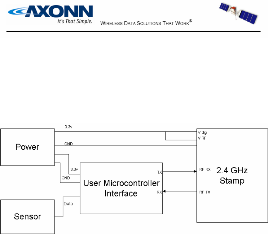
2. Typical Integration
Below is a block diagram of how a normal system using a 2.4 GHz Stamp would be
designed.
3. Product Specifications
3.1 Specifications
TBC
Axonn LLC Stamp User’s Guide-Document #9100-0160-01 Ver 1.0 4/7
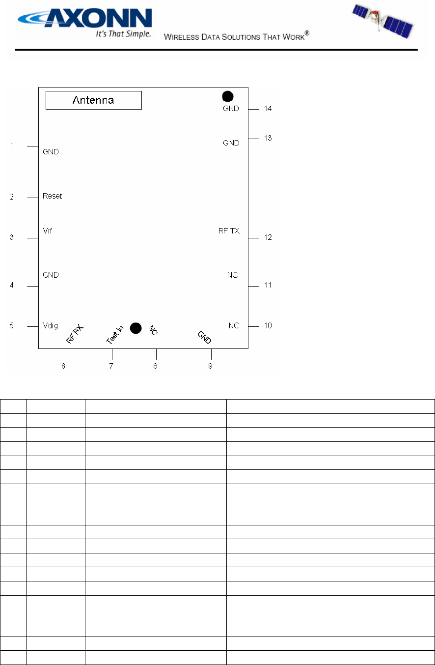
3.2 Pin Diagram
3.3 Pin Descriptions
Pin Pin Name Electrical Spec Note
1 GND Tie directly to host ground plane.
2 Reset DO NOT CONNECT For use with serial programming
3 VRF 3.3V +/-5% Powers the 2.4 GHz transceiver
4 GND
5 VDIG 3.3V +/-5% Powers digital circuitry
6 RF RX 3.3V TTL Output
Logic 0: <0.6V
Logic 1: >0.8*Vdig
Data Input
To be transmitted over 2.4 GHz radio
2400 baud
7 Test In DO NOT CONNECT For use with serial programming
8 NC
9 GND
10 NC
11 NC
12 RF TX 3.3V TTL Input
Logic 0: <0.6V
Logic 1: >0.8*Vdig
Data output
Information received over 2.4 GHz radio
2400 Baud
13 GND
14 GND

Axonn LLC Stamp User’s Guide-Document #9100-0160-01 Ver 1.0 5/7
Approximate Current Consumption (through Vdig and Vrf combined):
Maximum: 25mA
Sleep mode: 1-2µA
4. Air Interface
TBC
4.1 Frequency
TBC
4.2 Power
TBC
4.3 Timing
TBC
5. Serial User Interface
TBC
5.1 Message Protocol
TBC
5.2 Tips
TBC
5.3 Timing
TBC
5.4 Digital I/O
TBC
Axonn LLC Stamp User’s Guide-Document #9100-0160-01 Ver 1.0 6/7
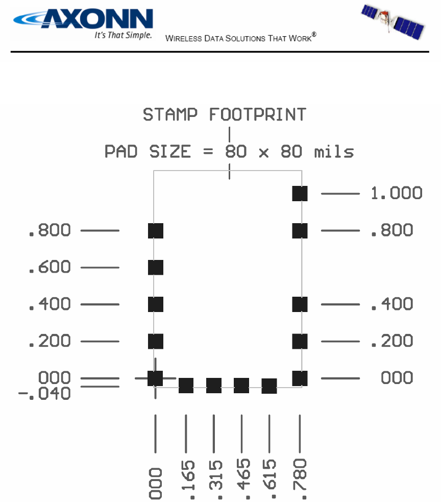
6. Mounting Guidelines
The figure below shows the recommended footprint for mounting the Stamp on its host
board.
7. Power Supply Requirements
TBC
8. Environmental Specifications
TBC
Axonn LLC Stamp User’s Guide-Document #9100-0160-01 Ver 1.0 7/7
9. Regulatory Approvals
FCC ID: L2V-STAMP IC:3989A-STAMP
THIS DEVICE COMPLIES WITH PART 15 OF THE FCC RULES.
OPERATION IS SUBJECT TO THE FOLLOWING TWO
CONDITIONS.
(1) THIS DEVICE MAY NOT CAUSE HARMFUL INTERFERENCE,
AND (2) THIS DEVICE MUST ACCEPT ANY INTERFERENCE
RECEIVED, INCLUDING INTERFERENCE THAT MAY CAUSE
UNDESIRED OPERATION.

The FCC requires the following notification for the device in compliance with 47CFR
15.105 for this Class B digital device. Full product test reports are available from Axonn
upon request.
NOTE: This equipment has been tested and found to c
omply with the limits for a Class B
digital device, pursuant to Part 15 of the FCC Rules. These limits are designed to provide
reasonable protection against harmful interference when the equipment is operated in a
residential environment. This equipment generates, uses, and can radiate radio frequency
energy and, if not installed and used in accordance with the instruction manual, may cause
harmful interference to radio communications. However, there is no guarantee that
interference will not occur in a particular installation. If this equipment does cause harmful
interference to radio or television reception, which can be determined by turning the
equipment off and on, the user is encouraged to try to correct the interference by one or
more of the following measures:
• Reorient or relocate the receiving antenna.
• Increase the separation between the equipment and receiver.
• Connect the equipment into an outlet on a circuit different from
that to which the receiver is connected.
• Consult the dealer or an experienced radio/TV technician for
help.
WARNING: Changes or modifications not expressly approved by Axonn may render the
device non-compliant to FCC and other regulatory body standards for operation and may
void the user’s authority to operate the equipment.
Accessory items that can be readily obtained from multiple retail outlets are not considered
to be special accessories and are not to be marketed with the equipment. Only those
accessory items provided by Axonn have been tested to ensure operation consistent with the
regulatory standards that the device is required to perform.
This device complies with Part 15 of the FCC Rules. Operation is subject to the following
two conditions: (1) This device may not cause harmful interference, and (2) this device
must accept any interference received, including interference that may cause undesired
operation.
This device will operate in accordance to the standards set forth by the CE Mark Directives
and standards R&TTE: ( EN 300 328), RFI: (EN61000-4-3:1996
+ A1:1998 + A2:2000), ESD: (EN61000-4-2: 1995 + A1:1998)
This ClassB digital apparatus complies with Canadian ICES-003.
NOTICE: This equipment complies with the FCC RF Exposure Limits. A minimum o
f 20
centimeters (8 inches) separation between the device and the user and all other persons
should be maintained.