SwipeSense MOD001 SwipeSense Wireless module User Manual
SwipeSense SwipeSense Wireless module
UserManual.wiki
>
SwipeSense
>
MOD001 User Manual
User Manual
Navigation menu
Upload a User Manual
Namespaces
Wiki Guide
HTML
PDF
Info
Views
User Manual
Discussion / Help
Navigation
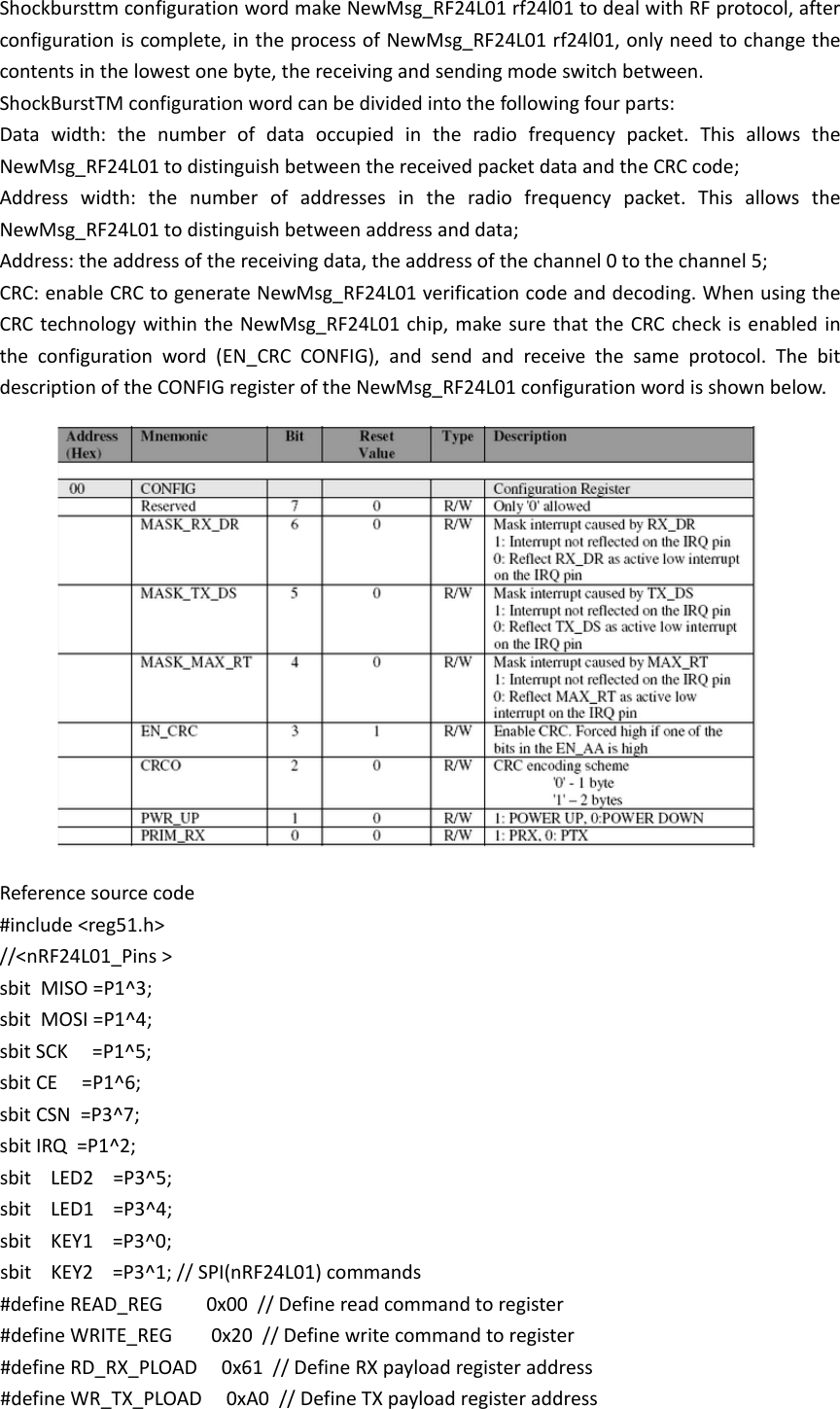
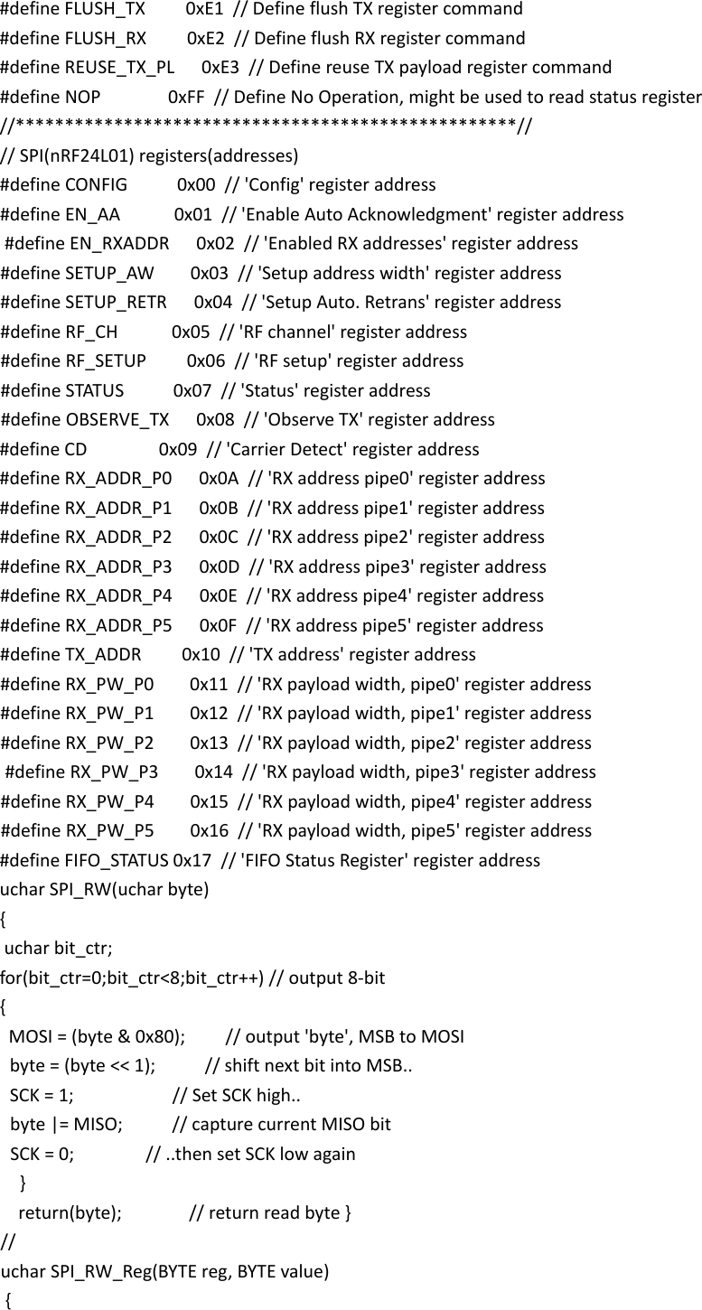
![uchar status; CSN = 0; // CSN low, init SPI transaction status = SPI_RW(reg); // select register SPI_RW(value); // ..and write value to it.. CSN = 1; // CSN high again return(status); // return nRF24L01 status byte } // uchar SPI_Read_Buf(BYTE reg, BYTE *pBuf, BYTE bytes) { uchar status,byte_ctr; CSN = 0; // Set CSN low, init SPI tranaction status = SPI_RW(reg); // Select register to write to and read status byte for(byte_ctr=0;byte_ctr<bytes;byte_ctr++) pBuf[byte_ctr] = SPI_RW(0); // CSN = 1; return(status); // return nRF24L01 status byte } // uchar SPI_Write_Buf(BYTE reg, BYTE *pBuf, BYTE bytes) { uchar status,byte_ctr; CSN = 0; status = SPI_RW(reg); for(byte_ctr=0; byte_ctr<bytes; byte_ctr++) // SPI_RW(*pBuf++); CSN = 1; // Set CSN high again return(status); // } // unsigned char nRF24L01_RxPacket(unsigned char* rx_buf) { unsigned char revale=0; // set in RX mode SPI_RW_Reg(WRITE_REG + CONFIG, 0x0f); // Set PWR_UP bit, enable CRC(2 bytes) & Prim:RX. RX_DR enabled.. CE = 1; // Set CE pin high to enable RX device dalay130us(); sta=SPI_Read(STATUS); // read register STATUS's value if(RX_DR) // if receive data ready (RX_DR) interrupt { CE = 0; // stand by mode SPI_Read_Buf(RD_RX_PLOAD,rx_buf,TX_PLOAD_WIDTH); // read receive payload from RX_FIFO buffer revale =1; } SPI_RW_Reg(WRITE_REG+STATUS,sta); // clear RX_DR or TX_DS or MAX_RT interrupt flag return revale; } // void nRF24L01_TxPacket(unsigned char * tx_buf) { CE=0; //SPI_Write_Buf(WRITE_REG+TX_ADDR,TX_ADDRESS, TX_ADR_WIDTH); // Writes TX_Address to nRF24L01](https://usermanual.wiki/SwipeSense/MOD001/User-Guide-2664017-Page-8.png)