SwipeSense MOD001 SwipeSense Wireless module User Manual
SwipeSense SwipeSense Wireless module
User Manual
SwipeSense Wireless module User Manual
V1.1
Introduction:
(1) Use 2.4 GHz global open ISM band free license
(2) The highest working rate 2Mbps, efficient GFSK modulation, anti-interference ability,
especially for industrial control occasions
(3) The built-in hardware CRC error detection and point to multipoint communication control.
(4) Low power 1.9 - 3.6V, standby mode state is 22uA; power down mode is 900nA
(5) Built in 2.4Ghz antenna, compact size
(6) The module can set up the address only when receiving the address of the machine to output
data (provide interrupt instructions), can directly take a variety of microcontroller, software
programming is very convenient
(7) Built in specialized regulator circuit, using various power supply including DC/DC switch power
supply have good communication effect
(8) Standard DIP spacing interface, easy for embedded applications
(9) Automatic packet handling, Auto packet transaction handling, With the optional built-in
package response mechanism, greatly reducing the packet loss rate.
(10) With the SC51 series microcontroller P0 port, the need to add 10K on the pull resistor, and
the rest of the port connection do not need.
(11) Other series MCU. If it is 5V, please refer to the series microcontroller IO export output
current size, if exceed 10mA and need to the series resistance divider, otherwise easy to burn
module! If is a 3.3V can direct and rf2401 module IO port line connection. Such as AVR series
microcontroller if it is 5V, the general series of resistance 2K.
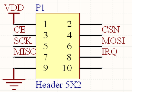
Typical interface circuit:
interface Introduction:
(1) the range of the VCC pin is between 1.9V~3.6V and cannot be outside of the range,
Over 3.6V will burn the module. Recommended voltage around 3.3V.
(2) except for power VCC and ground, the rest of the foot can be directly and ordinary 5V
microcontroller IO port directly connected without level conversion. Of course, about 3V
microcontroller more applicable.
(3) the hardware above no SPI microcontroller can also control this module, with ordinary
microcontroller IO mouth simulation SPI no real serial port intervention, just ordinary single-chip
IO port can, of course, with the serial port can also.
(4) 9 feet grounded, and the logical connection of the motherboard; 2 feet and 9 feet vacant.
(5) gill spacing of 2.54mm, standard DIP pin, if need other package interface, such as dense feet
pin, or other forms of interface can contact us custom.
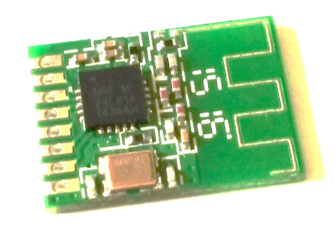
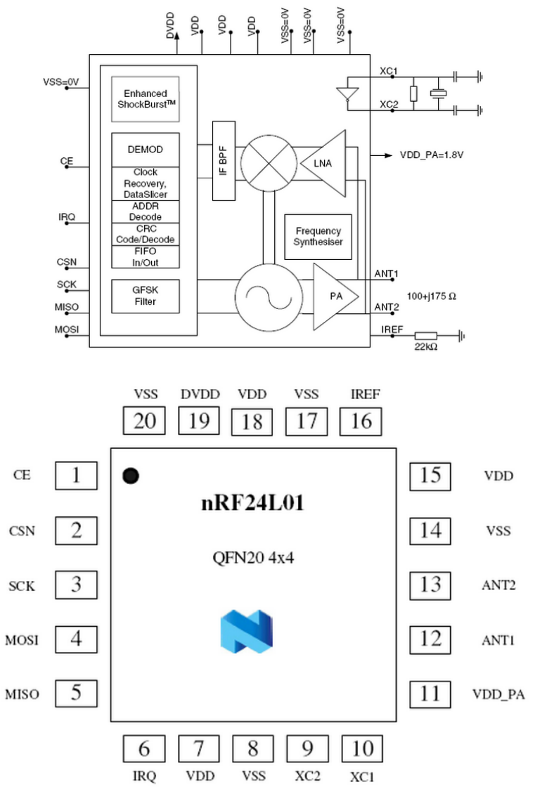
Module structure and pin output:
Msg_RF24L01
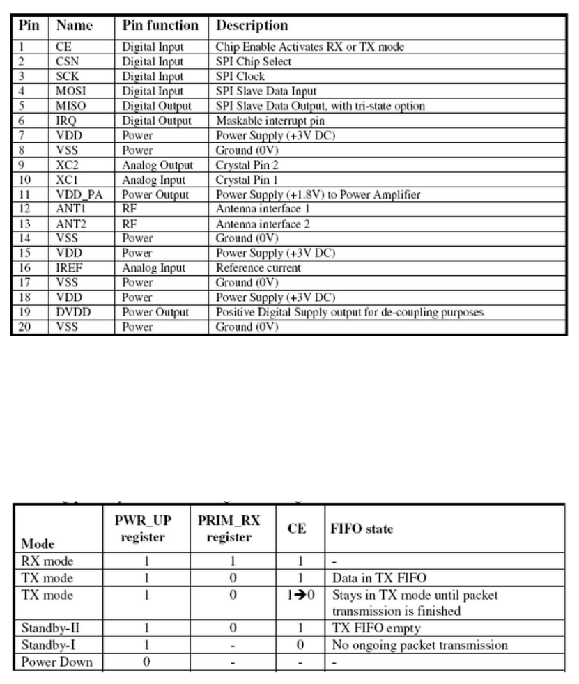
Operating mode
There are four kinds of working mode:
The mode of the idle mode of the transceiver mode is off mode
The working mode is determined by register PRIM_RX, register PWR_UP and CE, as shown in the
following table.
Transceiver mode
In receiving and transmitting mode enhanced shockbursttm transceiver mode, shockbursttm
mode transceiver and transceiver mode three, the transceiver mode by device configuration
word decision, specific configuration will be discussed in detail in the configuration part of the
device.
ShockBurstTM Enhanced transceiver mode
Enhanced shockbursttm transceiver mode, using the first in, first out stack area and low-speed
data from the microcontroller into, but a high speed (1Mbps transmission. Only in this way can
try to energy-saving. Therefore, using a low speed micro controller can also get very high radio
frequency data transmission rate. And RF protocol related all high-speed signal processing in
tablets were, this approach has three advantages: energy saving as much as possible; low system
cost (low speed microprocessor can also for high-speed RF emission); data stay in the air for a
short time, anti-interference. ShockBurstTM Enhanced technology also reduces the average
operating current of the whole system.
In the Enhanced ShockBurstTM transceiver mode, automatic processing of NewMsg_RF24L01
prefix and CRC check code. When receiving data, automatically put the prefix and CRC check code
to remove. In data transmission, automatic prefix and CRC code, in transmit mode, set the CE is
high, at least 10us. When the sending process completed. Enhanced ShockBurstTM 4.1.1.1
launch process
A. sends the address of the receiver and the data to send into NewMsg_RF24L01 by sequence; B.
is configured for CONFIG register, so that the sending mode is sent..
C. microcontroller CE (at least 10us), Enhanced NewMsg_RF24L01 launched ShockBurstTM
launch;
NewMsg_RF24L01 Enhanced ShockBurstTM D. emission
(1) powering the RF front end;
(2) RF data package (plus prefix, CRC check code);
(3) high speed emission packet;
(4) the launch is complete and the NewMsg_RF24L01 enters the idle state.
Enhanced ShockBurstTM 4.1.1.2 reception process
A. configure the address and packet size to receive;
B. configure the CONFIG register to make it into the receiving mode, the CE set high.
After 130us NewMsg_RF24L01, C. enters the monitoring state, waiting for the arrival of the
packet;
D. when receiving a correct packet (the correct address and CRC code), NewMsg_RF2401 rf2401
automatically the prefix, address and CRC displacement;
NewMsg_RF24L01 E. notify the microcontroller by setting the RX_DR (STATUS) of the STATUS
register to the microcontroller interrupt.;
F. microcontroller to read data from the NewMsg_RF2401;
After the completion of the G. all data, you can clear the STATUS register. NewMsg_RF2401 can
enter one of the four major models.
ShockBurstTM transceiver mode
ShockBurstTM transceiver mode can be compatible with Nrf2401a, 02, E1 and E2,
NewMsg-RF2401 documents before the specific look at the company.
Idle mode
NewMsg_RF24L01 idle mode is designed to reduce the average operating current, the biggest
advantage is that, to achieve energy saving, shorten the starting time of the chip. In idle mode,
the on-chip oscillator part is still at work, the work frequency of the current with the external
crystal.
Shutdown mode
In the shutdown mode, in order to get the minimum working current, the working current at this
time is about 900nA. In the shutdown mode, the content of the configuration word is maintained
in the NewMsg_RF2401 chip, which is the difference between the mode and the power off state.
Configure NewMsg_RF24L01 module
All of the configuration of the NewMsg_RF2401 is done by SPI, with 30 bytes of configuration
word.. We recommend NewMsg_RF24L01 rf24l01 work in enhanced shockbursttm transceiver
mode. This mode, system programming will be more simple and stability will be higher, therefore,
are highlighted below the NewMsg_RF24L01 rf24l01 configuration for device configuration
method of enhanced shockbursttm transceiver mode.
Shockbursttm configuration word make NewMsg_RF24L01 rf24l01 to deal with RF protocol, after
configuration is complete, in the process of NewMsg_RF24L01 rf24l01, only need to change the
contents in the lowest one byte, the receiving and sending mode switch between.
ShockBurstTM configuration word can be divided into the following four parts:
Data width: the number of data occupied in the radio frequency packet. This allows the
NewMsg_RF24L01 to distinguish between the received packet data and the CRC code;
Address width: the number of addresses in the radio frequency packet. This allows the
NewMsg_RF24L01 to distinguish between address and data;
Address: the address of the receiving data, the address of the channel 0 to the channel 5;
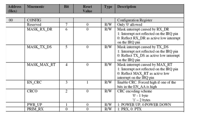
CRC: enable CRC to generate NewMsg_RF24L01 verification code and decoding. When using the
CRC technology within the NewMsg_RF24L01 chip, make sure that the CRC check is enabled in
the configuration word (EN_CRC CONFIG), and send and receive the same protocol. The bit
description of the CONFIG register of the NewMsg_RF24L01 configuration word is shown below.
Reference source code
#include <reg51.h>
//<nRF24L01_Pins >
sbit MISO =P1^3;
sbit MOSI =P1^4;
sbit SCK =P1^5;
sbit CE =P1^6;
sbit CSN =P3^7;
sbit IRQ =P1^2;
sbit LED2 =P3^5;
sbit LED1 =P3^4;
sbit KEY1 =P3^0;
sbit KEY2 =P3^1; // SPI(nRF24L01) commands
#define READ_REG 0x00 // Define read command to register
#define WRITE_REG 0x20 // Define write command to register
#define RD_RX_PLOAD 0x61 // Define RX payload register address
#define WR_TX_PLOAD 0xA0 // Define TX payload register address
#define FLUSH_TX 0xE1 // Define flush TX register command
#define FLUSH_RX 0xE2 // Define flush RX register command
#define REUSE_TX_PL 0xE3 // Define reuse TX payload register command
#define NOP 0xFF // Define No Operation, might be used to read status register
//***************************************************//
// SPI(nRF24L01) registers(addresses)
#define CONFIG 0x00 // 'Config' register address
#define EN_AA 0x01 // 'Enable Auto Acknowledgment' register address
#define EN_RXADDR 0x02 // 'Enabled RX addresses' register address
#define SETUP_AW 0x03 // 'Setup address width' register address
#define SETUP_RETR 0x04 // 'Setup Auto. Retrans' register address
#define RF_CH 0x05 // 'RF channel' register address
#define RF_SETUP 0x06 // 'RF setup' register address
#define STATUS 0x07 // 'Status' register address
#define OBSERVE_TX 0x08 // 'Observe TX' register address
#define CD 0x09 // 'Carrier Detect' register address
#define RX_ADDR_P0 0x0A // 'RX address pipe0' register address
#define RX_ADDR_P1 0x0B // 'RX address pipe1' register address
#define RX_ADDR_P2 0x0C // 'RX address pipe2' register address
#define RX_ADDR_P3 0x0D // 'RX address pipe3' register address
#define RX_ADDR_P4 0x0E // 'RX address pipe4' register address
#define RX_ADDR_P5 0x0F // 'RX address pipe5' register address
#define TX_ADDR 0x10 // 'TX address' register address
#define RX_PW_P0 0x11 // 'RX payload width, pipe0' register address
#define RX_PW_P1 0x12 // 'RX payload width, pipe1' register address
#define RX_PW_P2 0x13 // 'RX payload width, pipe2' register address
#define RX_PW_P3 0x14 // 'RX payload width, pipe3' register address
#define RX_PW_P4 0x15 // 'RX payload width, pipe4' register address
#define RX_PW_P5 0x16 // 'RX payload width, pipe5' register address
#define FIFO_STATUS 0x17 // 'FIFO Status Register' register address
uchar SPI_RW(uchar byte)
{
uchar bit_ctr;
for(bit_ctr=0;bit_ctr<8;bit_ctr++) // output 8-bit
{
MOSI = (byte & 0x80); // output 'byte', MSB to MOSI
byte = (byte << 1); // shift next bit into MSB..
SCK = 1; // Set SCK high..
byte |= MISO; // capture current MISO bit
SCK = 0; // ..then set SCK low again
}
return(byte); // return read byte }
//
uchar SPI_RW_Reg(BYTE reg, BYTE value)
{
uchar status; CSN = 0; // CSN low, init SPI transaction
status = SPI_RW(reg); // select register
SPI_RW(value); // ..and write value to it..
CSN = 1; // CSN high again
return(status); // return nRF24L01 status byte
}
//
uchar SPI_Read_Buf(BYTE reg, BYTE *pBuf, BYTE bytes)
{
uchar status,byte_ctr; CSN = 0; // Set CSN low, init SPI tranaction
status = SPI_RW(reg); // Select register to write to and read status byte
for(byte_ctr=0;byte_ctr<bytes;byte_ctr++)
pBuf[byte_ctr] = SPI_RW(0); // CSN = 1;
return(status); // return nRF24L01 status byte
}
//
uchar SPI_Write_Buf(BYTE reg, BYTE *pBuf, BYTE bytes)
{
uchar status,byte_ctr; CSN = 0;
status = SPI_RW(reg);
for(byte_ctr=0; byte_ctr<bytes; byte_ctr++) //
SPI_RW(*pBuf++);
CSN = 1; // Set CSN high again
return(status); //
}
//
unsigned char nRF24L01_RxPacket(unsigned char* rx_buf)
{
unsigned char revale=0; // set in RX mode
SPI_RW_Reg(WRITE_REG + CONFIG, 0x0f);
// Set PWR_UP bit, enable CRC(2 bytes) & Prim:RX. RX_DR enabled..
CE = 1; // Set CE pin high to enable RX device
dalay130us();
sta=SPI_Read(STATUS); // read register STATUS's value
if(RX_DR) // if receive data ready (RX_DR) interrupt
{ CE = 0; // stand by mode
SPI_Read_Buf(RD_RX_PLOAD,rx_buf,TX_PLOAD_WIDTH);
// read receive payload from RX_FIFO buffer revale =1; }
SPI_RW_Reg(WRITE_REG+STATUS,sta); // clear RX_DR or TX_DS or MAX_RT interrupt flag
return revale; }
//
void nRF24L01_TxPacket(unsigned char * tx_buf) {
CE=0;
//SPI_Write_Buf(WRITE_REG+TX_ADDR,TX_ADDRESS, TX_ADR_WIDTH); // Writes TX_Address t
o nRF24L01
//SPI_Write_Buf(WRITE_REG+RX_ADDR_P0,TX_ADDRESS,TX_ADR_WIDTH); // RX_Addr0 same as
TX_Adr for Auto.Ack
SPI_Write_Buf(WR_TX_PLOAD, tx_buf, TX_PLOAD_WIDTH); // Writes data to TX payload
SPI_RW_Reg(WRITE_REG + CONFIG, 0x0e);
// Set PWR_UP bit, enable CRC(2 bytes) & Prim:TX. MAX_RT & TX_DS enabled.. CE=1;
dalay10us(); CE=0; }
//
void nRF24L01_Config(void) {
//initial io CE=0; // chip enable CSN=1; // Spi disable
SCK=0; // Spi clock line init high CE=0;
SPI_RW_Reg(WRITE_REG + CONFIG, 0x0f);
// Set PWR_UP bit, enable CRC(2 bytes) & Prim:RX. RX_DR enabled..
SPI_RW_Reg(WRITE_REG + EN_AA, 0x01);
SPI_RW_Reg(WRITE_REG + EN_RXADDR, 0x01); // Enable Pipe0
SPI_RW_Reg(WRITE_REG + SETUP_AW, 0x02); // Setup address width=5 bytes
SPI_RW_Reg(WRITE_REG + SETUP_RETR, 0x1a); // 500us + 86us, 10 retrans...
SPI_RW_Reg(WRITE_REG + RF_CH, 0);
SPI_RW_Reg(WRITE_REG + RF_SETUP, 0x07); // TX_PWR:0dBm, Datarate:1Mbps, LNA:HCURR
SPI_RW_Reg(WRITE_REG+RX_PW_P0, RX_PLOAD_WIDTH);
SPI_Write_Buf(WRITE_REG + TX_ADDR, TX_ADDRESS, TX_ADR_WIDTH); SPI_Write_Buf(WRITE_
REG + RX_ADDR_P0, TX_ADDRESS, TX_ADR_WIDTH); CE=1; //
}
Limited Modular Approval
This RF Module is strictly limited to integration into three battery powered host devices. These
host information as below:
Manufacture: SwipeSense, Inc
Products: Wearable Dispenser (model: 2003.0),
Wall Sensor (model: 4004.0),
Badges (model: BAD001).
Integration into devices that are directly or indirectly connected to AC lines must add with Class II
Permissive Change. (OEM) Integrator has to assure compliance of the entire end product incl. the
integrated RF Module. Additional measurements (15B) and/or equipment authorizations (e.g
Verification) may need to be addressed depending on co-location or simultaneous transmission
issues if applicable. Integrator is reminded to assure that these installation instructions will not
be made available to the end user of the final host device.
With the documented max output power this RF Module meets the FCC SAR Exemption, so it
comply with any applicable RF exposure requirements in its final configuration. The RF Module is
powered by battery, the antenna is PCB antenna and the antenna gain is 0 dBi. The final host
device, into which this RF Module is integrated" has to be labeled with an auxiliary label stating
the FCC ID of the RF Module, such as “Contain FCC ID: 2AB5RMOD001"."
FCC RF Exposure Information and Statement
This equipment complies with FCC RF radiation exposure limits set forth for an uncontrolled
environment.
This device complies with part 15 of the FCC rules. Operation is subject to the following two
conditions: (1) this device may not cause harmful interference, and (2) this device must accept
any interference received, including interference that may cause undesired operation.
NOTE: The manufacturer is not responsible for any radio or TV interference caused by
unauthorized modifications to this equipment. Such modifications could void the user’s authority
to operate the equipment.
NOTE: This equipment has been tested and found to comply with the limits for a Class B digital
device, pursuant to part 15 of the FCC Rules. These limits are designed to provide reasonable
protection against harmful interference in a residential installation. This equipment generates
uses and can radiate radio frequency energy and, if not installed and used in accordance with the
instructions, may cause harmful interference to radio communications. However, there is no
guarantee that interference will not occur in a particular installation. If this equipment does
cause harmful interference to radio or television reception, which can be determined by turning
the equipment off and on, the user is encouraged to try to correct the interference by one or
more of the following measures:
- Reorient or relocate the receiving antenna.
- Increase the separation between the equipment and receiver.
-Connect the equipment into an outlet on a circuit different from that to which the receiver is
connected.
-Consult the dealer or an experienced radio/TV technician for help
- This device and its antenna(s) must not be co-located or operating in conjunction with any other
antenna or transmitter.