TCL Technoly Electronics 06 Bluetooth Module User Manual BM63 Rev2
TCL Technoly Electronics (Huizhou) Co., Ltd. Bluetooth Module BM63 Rev2
Contents
- 1. BM63 user manual
- 2. BM63 User Manual_Rev2
BM63 User Manual_Rev2

BM63SPKA1MGA
5F, No.5, Industry E. Rd. VII, Hsinchu Science Park, Hsinchu city 30077, Taiwan, R.O.C Version:1.2
Phone: 886-3-577-8385 10/15/2014
Fax: 886-3-577-8501
BM63SPKA1MGA
Bluetooth 3.0 Digital Audio Output Module

BM63SPKA1MGA
ISSC Confidential (Version: 1.2) - 2 - 10/15/2014
Product Description
The ISSC BM63SPKA1MGA is a highly integrated Bluetooth 3.0 digital audio
output module, designed for high data rate, short-range wireless
communication in the 2.4 GHz ISM band. With the built-in ISSC Bluetooth
stack, profiles and digital audio interface, the ISSC BM63SPKA1MGA can
combine the external DSP and codec to provide high performance Bluetooth
audio.
Features
Main Chip: ISSC IS2063GM(Flash version)
Bluetooth 3.0 compliant
Max. +4dBm Class 2 output power
Receiver Sensitivity: GFSK typical -89dBm, π/4 PSK typical -90dBm,
8DPSK typical -83dBm
Piconet and Scatter net support
CVSD, A-law, -law, mSBC CODEC algorithms for voice applications
Support SONY new feature
SBC/AAC decode for Bluetooth audio streaming
Microphone input and audio line-in support
Built-in four language voice prompt (Chinese/English/Spanish/French)
Support PCM and I2S digital audio interface
Built-in 350mAH Li-ion battery charger
HSP 1.2, HFP 1.6, A2DP 1.2, AVRCP 1.5,SPP 1.0 profiles supported
Support USB 1.1 DFU and BC1.2/Apple charger detection
USB BC1.2 charger detection for DCP/CDP/SDP
Apple Charger: 2.5W, 5W, 10W, 12.5W
3.3V operating voltage
Built-in program ROM and 64Kb EEPROM
51 pins for SMT module Size: 15mmx32mm
Built-in PCB Antenna
RoHS compliant
BM63SPKA1MGA
ISSC Confidential (Version: 1.2) - 3 - 10/15/2014
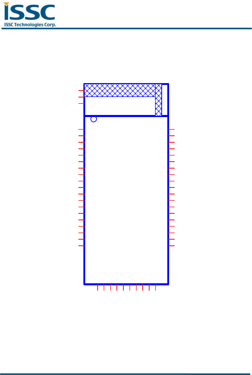
Module Pin Out Diagram
BM63SPKA1MGA
P02 43
P31 42
P33 41
P36 40
DP 39
ADAP_IN
24
DM 38
VDD_IO
23
EAN 37
P03 36
P05 47
P00 35
LED3
29
AOHPM
6
DR0
1
RFS0
2
SCLK0
3
DT0
4
AOHPL
7
MICBIAS
10
MICN1
8
MICP1
9
AIR
11
AIL
12
P04
18
SYS_PWR
27
BAT_IN
25
AMB_DET
26
P30 46
P20 44
CODEC_VO
22
AOHPR
5
P12
13
P27 45
ANT1
49
ANT2
50
ANT3
51
HCI_RXD
20
HCI_TXD
21
P13
14
RST_N
15 P35 34
P37 33
GND 32
LED1 31
LED2 30
P01
16
P24
17
PWR(MFB)
28
GND 48
P15
19
BM63SPKA1MGA
ISSC Confidential (Version: 1.2) - 4 - 10/15/2014
Pin Definition for Flash module
Pin No.
Pin type
Name
Description
1
I
DR0
I2S interface: Digital Left/Right Data from ADC
2
O
RFS0
I2S interface: DAC Left/Right Clock
3
O
SCLK0
I2S interface: Bit Clock
4
O
DT0
I2S interface: Digital Left/Right Data to DAC
5
O
AOHPR
R-channel analog headphone output
6
O
AOHPM
Headphone common mode output/sense input.
7
O
AOHPL
L-channel analog headphone output
8
I
MICN1
MIC 1 mono differential analog negative input
9
I
MICP1
MIC 1 mono differential analog positive input
10
P
MICBIAS
Electric microphone biasing voltage
11
I
AIR
R-channel single-ended analog input
12
I
AIL
L-channel single-ended analog input
13
I/O
P12
GPIO, default pull-high input
1. KEY PIN for FT Test
2. EEPROM clock SCL
14
I/O
P13
GPIO, default pull-high input
1. KEY PIN for FT Test
2. EEPROM data SDA
15
I
RST_N
KEY PIN for FT Test
System Reset Pin (Low active)
16
I/O
P01
GPIO, default pull-high input
BAT_CHK_EN
17
I/O
P24
GPIO, default pull-high input
1. KEY PIN for FT Test
2. System Configuration:
H: Boot Mode
L: Boot Mode with P2_0 low combination
18
I/O
P04
GPIO, default pull-high input.
19
I/O
P15
GPIO, default pull-high input
20
I
HCI_RXD
KEY PIN for FT Test
1-bit serial data received from MCU through UART
21
O
HCI_TXD
KEY PIN for FT Test
1-bit serial data transmitted to MCU through UART
22
P
CODEC_VO
3.1V LDO output for CODEC power
23
P
VDD_IO
I/O power supply input
BM63SPKA1MGA
ISSC Confidential (Version: 1.2) - 5 - 10/15/2014
Pin No.
Pin type
Name
Description
24
P
ADAP_IN
Power adaptor input
25
P
BAT_IN
Battery input
26
P
AMB_DET
ADC analog input 1
27
P
SYS_PWR
System Power Output
28
I
PWR(MFB)
Multi-Function Push Button key
29
I
LED3
LED Driver 3
30
I
LED2
LED Driver 2
31
I
LED1
LED Driver 1
32
P
GND
Ground Pin
33
I/O
P37
GPIO, default pull-high input
34
I/O
P35
GPIO, default pull-high input (LF/ES samples)
Default pull-low input (CS/MP samples)
Charger Enable
35
I/O
P00
GPIO, default pull-high input
UART TX_IND signal to wake up MCU
36
I/O
P03
GPIO, default pull-high input
UART RX_IND signal to wake up BT
(Note: HCI_RXD can also be used to wake up BT)
37
I
EAN
Embedded ROM/External Flash enable
H: Embedded; L: External Flash
38
I/O
DM
USB Differential data bus
Data -
39
I/O
DP
USB Differential data bus
Data +
40
I/O
P36
GPIO, default pull-high input
41
I/O
P33
GPIO, default pull-high input
ICHG1
42
I/O
P31
GPIO, default pull-high input
ICHG0
43
I/O
P02
GPIO, default pull-high input
44
I/O
P20
GPIO, default pull-high input
1. KEY PIN for FT Test
2. System Configuration,
H: Application
L: Baseband(IBDK Mode)
45
I/O
P27
GPIO, default pull-high input
46
I/O
P30
GPIO, default pull-high input
BM63SPKA1MGA
ISSC Confidential (Version: 1.2) - 6 - 10/15/2014
Pin No.
Pin type
Name
Description
Line-in Detector
47
I/O
P05
GPIO, default pull-high input
Charger Status
48
P
GND
Ground Pin
49
P
ANT1
Antenna modification point
50
P
ANT2
Antenna modification point
51
P
ANT3
Antenna modification point
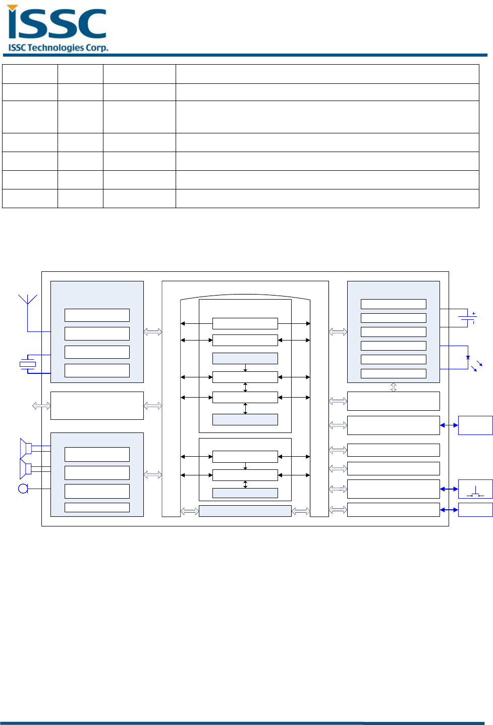
Block Diagram
Common RAM
BT 3.0 Digital Core
ROM
Interrupts
BUS
HCI/UART
GPIOs (Buttons)
I2C (GPIOs or H/W)
RAM
MCU Core
DSP Core
Memory Controller
DMA Controller
Modem + MAC
DSP ROM/RAM
PMU
Battery Charger
LDO
SAR_ADC
LED Driver * 2
BUCK
Power Switch
BT 3.0
Transceiver
Synthesizer
RF Transmitter
RF Receiver
XTAL + POR
Misc. PMU logic
EEPROM
Buttons
ULPC 32KHz
SPI
Flash
Audio Codec
Stereo DAC
Stereo ADC
Anti-Pop
Audio Digital Core
I2S/PCM
Module
External
MCU

BM63SPKA1MGA
ISSC Confidential (Version: 1.2) - 7 - 10/15/2014
Digital Audio Interface
Support I2S and PCM interface
Sampling Rate : 8K, 16K, 44.1K, 48K, 88.2K, 96K
Word Length: 16 bits, 24 bits
4 application modes
BM63SPKA1MGA
ISSC Confidential (Version: 1.2) - 8 - 10/15/2014
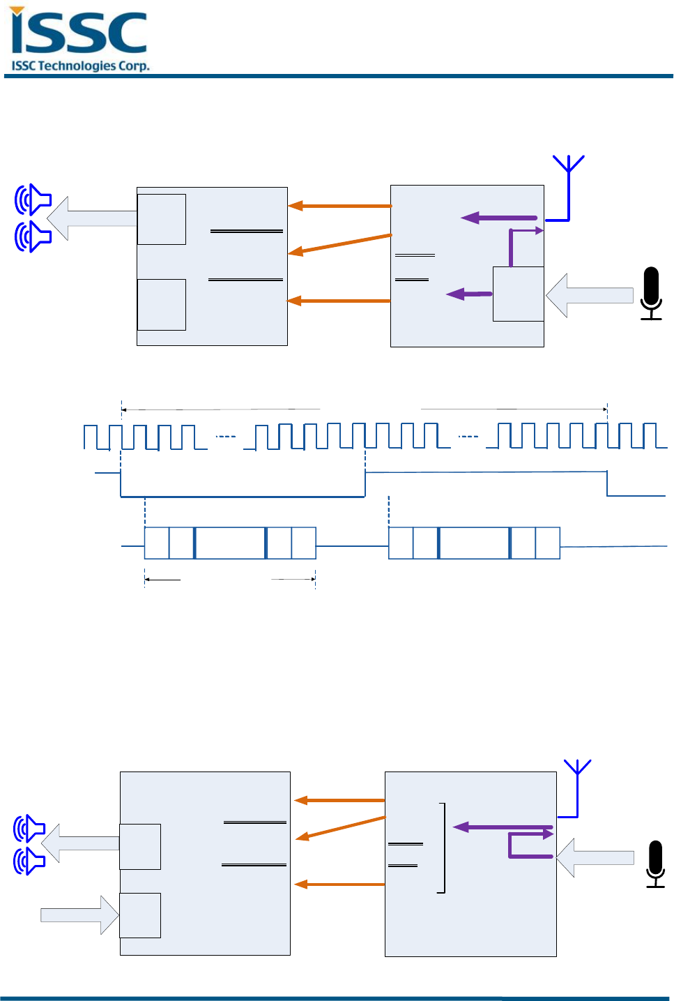
Mode 1: I2S Master
BCLK
ADCLRC
DACLRC
ADCDAT
DACDAT
Slave
SCLK0
RFS0
TFS0
DR0
DT0
Master
External CODEC/DSP BM63
DAC
ADC ADC
A2DP/SCO
SCO
LineIn
Bn-1
RFS0
SCLK0
DR0/DT0 Bn-2 B1B0Bn-1 Bn-2 B1B0
Left Channel Right Channel
1/fs
Word Length
or
Solutions with mic and line-in analog input with I2S audio output
Mic for Bluetooth SCO link
Line-in for external audio playback(for high SNR requirement)
BCLK
ADCLRC
DACLRC
ADCDAT
DACDAT
Slave
SCLK0
RFS0
TFS0
DR0
DT0
Master
External CODEC/DSP BM63
A2DP/SCO
DAC
LineIn
SCO
BM63SPKA1MGA
ISSC Confidential (Version: 1.2) - 9 - 10/15/2014
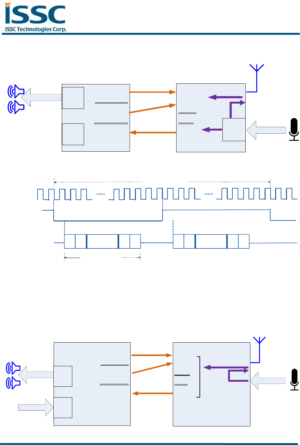
Mode 2: I2S Slave
BCLK
ADCLRC
DACLRC
ADCDAT
DACDAT
Master
SCLK0
RFS0
TFS0
DR0
DT0
Slave
External CODEC/DSP BM63
DAC
ADC ADC
A2DP/SCO
SCO
LineIn
Bn-1
RFS0
SCLK0
DR0/DT0 Bn-2 B1B0Bn-1 Bn-2 B1B0
Left Channel Right Channel
1/fs
Word Length
or
Solutions with mic and line-in analog input with I2S audio output
Mic for Bluetooth SCO link
Line-in for external audio playback(for high SNR requirement)
BCLK
ADCLRC
DACLRC
ADCDAT
DACDAT
Master
SCLK0
RFS0
TFS0
DR0
DT0
Slave
External CODEC/DSP BM63
A2DP/SCO
DAC
LineIn
SCO
BM63SPKA1MGA
ISSC Confidential (Version: 1.2) - 10 - 10/15/2014
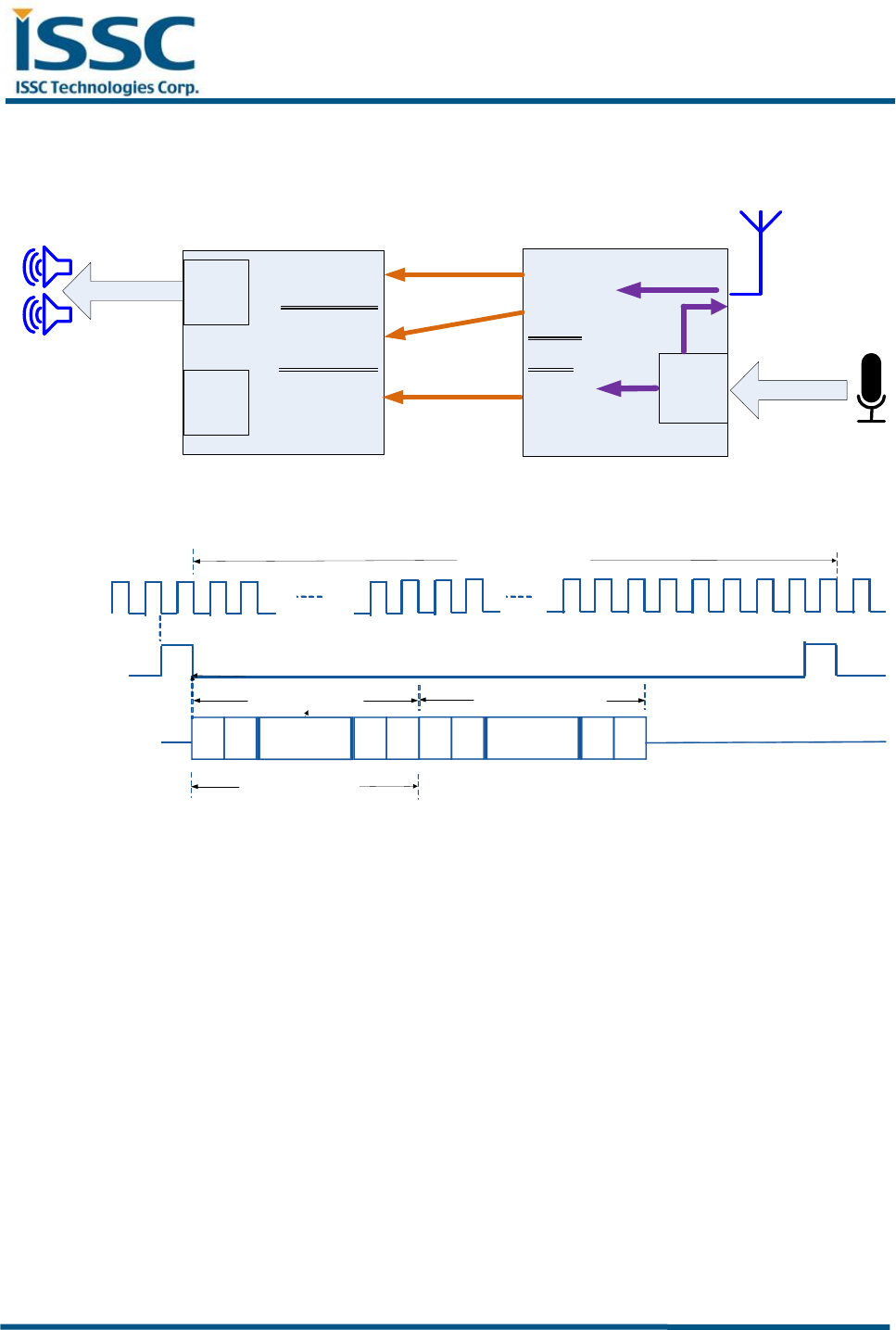
Mode 3: PCM master
BCLK
ADCLRC
DACLRC
ADCDAT
DACDAT
Slave
SCLK0
RFS0
TFS0
DR0
DT0
Master
External CODEC/DSP BM63
DAC
ADC ADC
A2DP/SCO
SCO
LineIn
Bn-1
RFS0
SCLK0
DR0/DT0 Bn-2 B1B0Bn-1 Bn-2 B1B0
Left Channel
1/fs
Word Length
Right Channel
BM63SPKA1MGA
ISSC Confidential (Version: 1.2) - 11 - 10/15/2014
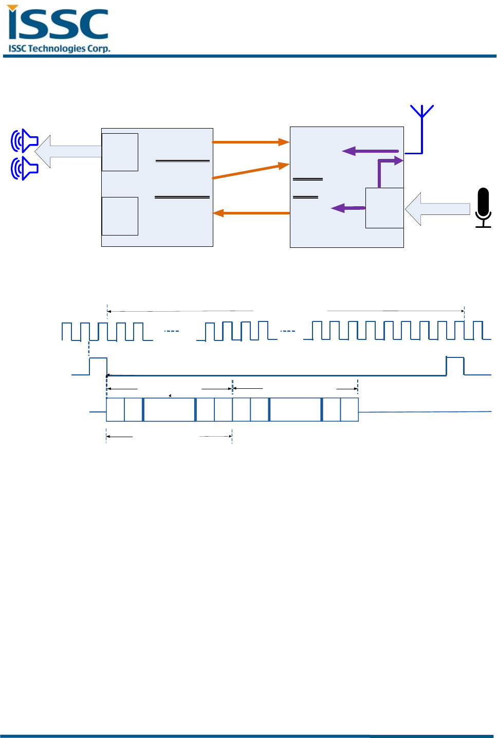
Mode 4: PCM slave
BCLK
ADCLRC
DACLRC
ADCDAT
DACDAT
Master
SCLK0
RFS0
TFS0
DR0
DT0
Slave
External CODEC/DSP BM63
DAC
ADC ADC
A2DP/SCO
SCO
LineIn
Bn-1
RFS0
SCLK0
DR0/DT0 Bn-2 B1B0Bn-1 Bn-2 B1B0
Left Channel
1/fs
Word Length
Right Channel
BM63SPKA1MGA
ISSC Confidential (Version: 1.2) - 12 - 10/15/2014
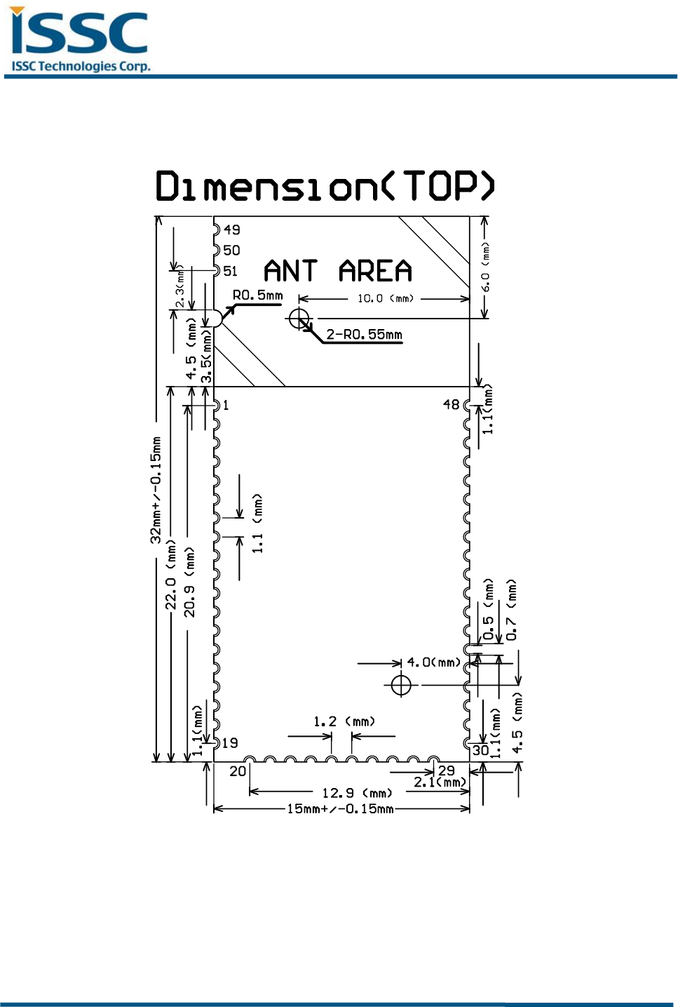
Outline Dimension (Module Foot print)
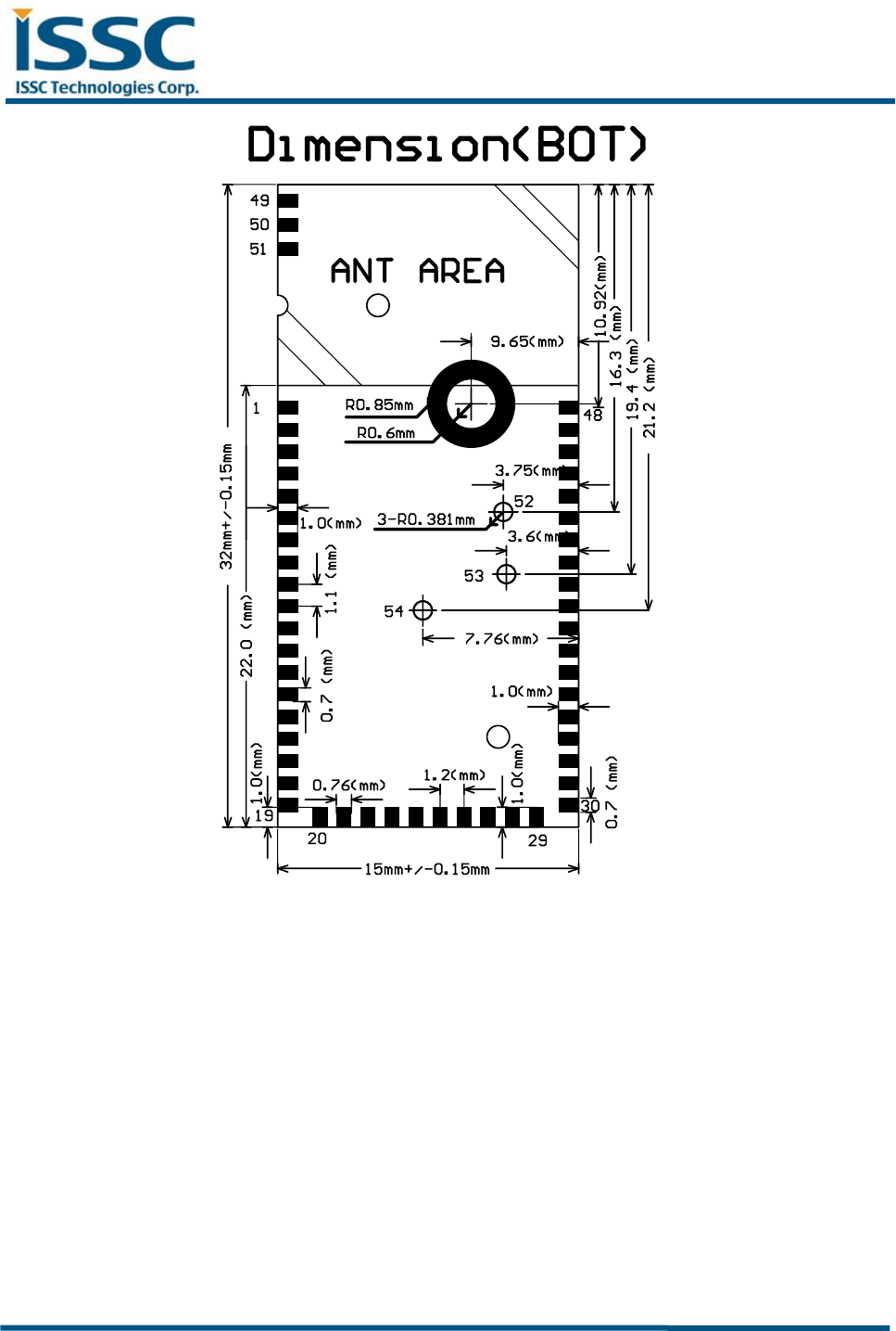
BM63SPKA1MGA
ISSC Confidential (Version: 1.2) - 13 - 10/15/2014
BM63SPKA1MGA
ISSC Confidential (Version: 1.2) - 14 - 10/15/2014
Electrical Characteristics
Table 1: Absolute Maximum Voltages
Min
Max
Storage Temperature
-40ºC
+85ºC
ESD: Human Body Mode
±2KV
ESD: Machine Mode
±200V
ESD: Charge Device Mode
±200V
Core supply voltage
VDD_CORE, AVDD_PLL
1.14V
1.26V
RF supply voltage
VCC_RF
1.22V
1.34V
SAR supply voltage
AVDD_SAR
1.62V
1.98V
Codec supply voltage
VDD_AUDIO
2.7V
3.0V
I/O voltage
VDD_IO
3.6V
Supply voltage
BK_VDD
4.5V
3V1_VIN
4.5V
BAT_IN
3.0
4.5V
ADAP_IN
4.5
7.0V
LED
5.1V
Power switch
7.0V
Table 2: Recommended Operating Conditions
Min
Typ
Max
Storage Temperature
-10ºC
+25ºC
+60ºC
Core supply voltage
VDD_CORE, AVDD_PLL
1.14V
1.2V
1.26V
RF supply voltage
VCC_RF
1.22V
1.28V
1.34V
SAR supply voltage
AVDD_SAR
1.62V
1.8V
1.98V
Codec supply voltage
VDD_AUDIO
2.7V
3.0V
I/O voltage
VDD_IO
2.7V
3.0V
3.3V
Supply voltage
BK_VDD
3V
4.3V
3V1_VIN
3V
4.3V
BAT_IN
3V
4.3V
ADAP_IN
4.5V
6.0V
LED
4.3V
5.0V
Power switch
1.8V
6.0V
BM63SPKA1MGA
ISSC Confidential (Version: 1.2) - 15 - 10/15/2014
Table 3: BUCK switching regulator
Normal Operation
Min
Typ
Max
Unit
Operation Temperature
-40
85
℃
Input Voltage (VIN)
3.0
3.8
4.5
V
Output Voltage (VOUT)
(ILOAD=70mA, VIN=4V)
1.7
1.80
2.05
V
Output Voltage Accuracy
±5
%
Output Voltage Adjustable Step
50
mV/Step
Output Adjustment Range
-0.1
+0.25
V
Output Ripple
10
15
mVRMS
Average Load Current (ILOAD)
120
mA
Settling Time
(start-up time)
EN or VIN to VOUT
1.2
2
ms
Conversion
efficiency
@BAT=3.8V
ILOAD = 50mA
88
%
ILOAD ≥ 10mA (PWM)
70
ILOAD ≥ 10mA (PFM)
80
ILOAD ≥ 250μA (PFM)
65
70
Switching Frequency
800
KHz
PWM/PFM Switching Point
by F/W
mA
Start-up Current Limit
0
50
210
mA
Start-up Inrush
Current
ILOAD = 10mA
400
mA
Quiescent Current
PWM
1000
μA
PFM
30
40
Output Current (Peak)
200
mA
Load Regulation (ILOAD = 10 ~ 100mA)
1
mV/mA
Line Regulation (3.2V < VIN < 4.2V)
0.03
(30)
%/V
(mV/V)
EN threshold
Logic Low Voltage (VIL)
0.4
V
Logic High Voltage (VIH)
1.62
V
EN current
10
nA
Shutdown Current
<1
μA
BM63SPKA1MGA
ISSC Confidential (Version: 1.2) - 16 - 10/15/2014
Table 4: Low Drop Regulation
Min
Typ
Max
Unit
Operation Temperature
-40
85
℃
Input Voltage (VIN)
3.0
4.5
V
Output Voltage (VOUT)
(1) VOUT_CODEC
(2) VOUT_IO
VOUT = 2.9V
(2.4~3.4V)
2.9
V
VOUT = 1.8V
(1.3~2.3V)
1.8
Accuracy (VIN=3.7V, ILOAD=100mA, 27’C)
±5
%
Output Voltage Adjustable Step
67
100
mV/Step
Output Adjustment Range
±0.5
V
Start-up Inrush Current
ILOAD=10mA
200
400
mA
Settling Time (start-up time)
EN or VIN to VOUT
250
500
μs
Output Current (Average)
VOUT
100
mA
Output Current (Peak)
VOUT
150
mA
Drop-Out Voltage
(ILOAD = maximum output current)
300
mV
Quiescent Current
(excluding load, ILOAD < 1mA)
45
μA
Quiescent Current
(excluding load, ILOAD < 100μA)
N/A
μA
Load Regulation (Iload = 0mA to 100mA), ΔVOUT
Note: 0.4(mV/mA) * (100mA-0mA)=40mV
40
(0.4)
mV
(mV/mA)
Line Regulation (VOUT+0.3V<VIN<4.5V
7
10
mV/V
EN threshold
Logic Low Voltage (VIL)
0.4
V
Logic High Voltage (VIH)
1.62
V
EN current
10
nA
Shutdown Current (*1)
<1
μA
BM63SPKA1MGA
ISSC Confidential (Version: 1.2) - 17 - 10/15/2014
Table 5: Battery Charger
Charging Mode (BAT_IN rising to 4.2V)
Min
Typ
Max
Unit
Operation Temperature
-40
85
℃
Input Voltage (VIN)
Note: It needs more time to get battery fully charged when
VIN=4.5V
4.5
5.0
7.0
V
Supply current to charger only
3
4.5
mA
Battery trickle charge current
(BAT_IN < trickle charge voltage threshold)
0.1C
mA
Maximum Battery
Fast Charge Current
Note: ENX2=0
Headroom > 0.7V
(ADAP_IN=5V)
170
200
240
mA
Headroom = 0.3V
(ADAP_IN=4.5V)
160
180
240
mA
Maximum Battery
Fast Charge Current
Note: ENX2=1
Headroom > 0.7V
(ADAP_IN=5V)
330
370
420
mA
Headroom = 0.3V
(ADAP_IN=4.5V)
180
220
270
mA
Minimum Step
1
mA
Trickle Charge Voltage Threshold
3
V
Float Voltage
4.158
4.2
4.242
V
Battery Charge Termination Current,
% of Fast Charge Current
10
%
Standby Mode (BAT_IN falling from 4.2V)
Supply current to charger only
2
4
mA
Battery Current
-1
μA
Battery Recharge Current
Note: C Battery Capacity (*1)
0.25C
mA
BM63SPKA1MGA
ISSC Confidential (Version: 1.2) - 18 - 10/15/2014
Table 6: Audio codec ADC
Conditions
Min
Typ
Max
Unit
Temperature
-40
25
85
℃
Resolution
16
Bits
Input sample rate, Fsample
8KHz for MIC
44.1/48KHz for Line-in
8
48
KHz
Signal to Noise Ratio
(SNR @MIC or Line-in mode)
fin=1KHz
B/W=20~20KHz
(A-weighted)
THD+N < 1%
2.26Vpp input
8KHz
90
92
dB
44.1/
48KHz
90
92
Digital Gain
-54
4.85
dB
Digital Gain Resolution
2~6
dB
MIC Boost Gain
20
PGA Analog Gain
-6
26
dB
Analog Gain step
1
dB
Input full-scale at maximum
gain (differential)
4
(AVDD=2.8V)
mVRMS
Input full-scale at minimum
gain (differential)
Note:
Input VPP=0.8*AVDD
800
(AVDD=2.8V)
mVRMS
3dB bandwidth
20
KHz
Microphone mode
input impedance
Input impedance
6
10
KΩ
Input capacitance
20
pF
THD+N (microphone input)
@30mVRMS input
0.02
%
THD+N (line input)
0.04
%
ADC channels
2
Analog supply voltage
2.6
2.8
3.0
V
Digital supply voltage
1.08
1.2
1.32
V
Crosstalk @line-in mode
42
45
48
dB
BM63SPKA1MGA
ISSC Confidential (Version: 1.2) - 19 - 10/15/2014
MIC AMP
+
-
LINE AMP
+
-
MICP1
MICN1
AIL
1-bit
SD ADC
Digital
Codec
DSP
Core
MIC Boost Gain
0dB or 20dB
PGA Analog Gain
-6 ~ 26dB in 1dB step
ADC Digital Gain
-54 ~ 4.85dB
Fixed in 0dB now
DSP Digital Gain
-96 ~ 0dB in 6dB step
Fixed in 0dB now
System Gain = MIC Boost Gain + PGA Analog Gain + ADC Digital Gain + DSP Digital Gain
MIC Boost Gain and PGA Gain are controlled by DSP F/W
(1) MIC mode:
(a) There are 16 gain levels: 46/43/40/37/34/31/28/25/22/19/16/13/10/7/4/0 dB
(b) 46/43/40/37 dB gain levels are normally used for MIC mode
(2) Line-in mode:
(a) MIC boost gain = 0 dB
(b) PGA analog gain = 0 dB
(c) ADC digital gain = 0 dB
(d) DSP digital gain = 0 dB
(e) Gain control for line-in mode is recommended to be done by DAC side
Note: For I2S digital audio output, no gain control in BM63 so far and it is controlled by external DAC
MIC AMP
+
-
LINE AMP
+
-
MICP1
MICN1
AIL
1-bit
SD ADC
Digital
Codec
DSP
Core
MIC Boost Gain
0dB or 20dB
PGA Analog Gain
-6 ~ 26dB in 1dB step
ADC Digital Gain
-54 ~ 4.85dB
Fixed in 0dB now
DSP Digital Gain
-96 ~ 0dB in 6dB step
Fixed in 0dB now
BT
RF/MAC
External
MCU
External
DSP/DAC
(YDA174)
I2S
I2C
Digital/Analog
Gain Control
UART
A2DP down link
&
SCO down link
SCO up link
Line-in mode
BM63SPKA1MGA
ISSC Confidential (Version: 1.2) - 20 - 10/15/2014
Table 7: Transmitter section for BDR (25℃)
Min
Typ
Max
Bluetooth
specification
Unit
Maximum RF transmit power
2.0*
5.0
-6 to 4
dBm
RF power variation over temperature
range with compensation disabled
±2.0
dB
RF power control range
18
≥16
dB
RF power range control resolution
±0.5
dB
20dB bandwidth for modulated
carrier
925
≤1000
KHz
ACP
Note:
F0=2441MHz
F = F0±2MHz
-42
-40
≤-20
dBm
F = F0±3MHz
-49
-48
≤-40
dBm
F = F0±>3MHz
-57
-53
≤-40
dBm
∆f1avg maximum modulation
145
175
140<∆f1avg<175
KHz
∆f2max maximum modulation
120
135
140
≥115
KHz
∆f2avg/∆f1avg
0.9
0.95
≥0.80
ICFT
4.5
8
10.5
±75
KHz
Drift rate
3.3
5
7.0
≤20
KHz/50
us
Drift (single slot packet)
12
≤40
KHz
2nd harmonic content
-42
≤-30
dBm
3rd harmonic content
-45
≤-30
dBm
* The transmit power is calibrated in MP.
BM63SPKA1MGA
ISSC Confidential (Version: 1.2) - 21 - 10/15/2014
Table 8 Transmitter section for EDR (25℃)
Min
Typ
Max
Bluetooth
specification
Unit
Relative transmit power
-1.2
-4 to 1
dB
π/4 DQPSK max
carrier frequency
stability
|ωo| freq. error
2.5
5
≤10 for all blocks
KHz
|ωi| initial freq. error
2.5
5
≤75 for all blocks
KHz
|ωo+ωi|
block freq. error
5
10
≤75 for all blocks
KHz
8DPSK max
carrier frequency
stability
|ωo| freq. error
2.5
5
≤10 for all blocks
KHz
|ωi| initial freq. error
2.5
5
≤75 for all blocks
KHz
|ωo+ωi|
block freq. error
5
10
≤75 for all blocks
KHz
π/4 DQPSK
modulation
accuracy
RMS DEVM
7
12.2
≤20
%
99% DEVM
PASS
≤30
%
Peak DEVM
25
≤35
%
8DQPSK
modulation
accuracy
RMS DEVM
7
≤13
%
99% DEVM
PASS
≤20
%
Peak DEVM
20
≤25
%
In-band spurious
emissions
Note:
F0=2441MHz
F > F0+3MHz
<-52
≤-40
dBm
F < F0-3MHz
<-53
≤-40
dBm
F = F0-3MHz
-46
≤-40
dBm
F = F0-2MHz
-34
≤-20
dBm
F = F0-1MHz
-34
≤-26
dBm
F = F0+1MHz
-37
≤-26
dBm
F = F0+2MHz
-34
≤-20
dBm
F = F0+3MHz
-46
≤-40
dBm
EDR differential phase encoding
100
≥99
%
BM63SPKA1MGA
ISSC Confidential (Version: 1.2) - 22 - 10/15/2014
Table 9 Receiver section for BDR (25℃)
Frequency
(GHz)
Min
Typ
Max
Bluetooth
specification
Unit
Sensitivity at 0.1%
BER for all basic rate
packet types
2.402
-89
≤-70
dBm
2.441
-89
2.480
-89
Maximum received signal at 0.1% BER
0
≥-20
dBm
Continuous power
required to block
Bluetooth reception
(for input power of
-67dBm with 0.1%
BER) measured at
the unbalanced port
of the balun
0.030–2.000
-7
-10
dBm
2.000-2.400
-10
-27
2.500-3.000
-11
-27
3.000-12.75
-7
-10
C/I co-channel
6
≤11
dB
Adjacent channel
selectivity C/I
Note: F0=2441MHz
F = F0+1MHz
-6
≤0
dB
F = F0-1MHz
-6.5
≤0
dB
F = F0+2MHz
-36
≤-30
dB
F = F0-2MHz
-28
≤-9
dB
F = F0-3MHz
-31
≤-20
dB
F = F0+5MHz
-48
≤-40
dB
F = Fimage
-28
≤-9
dB
Maximum level of inter-modulation
interferers
-37
≥-39
dBm
Spurious output level
N/A
dBm/Hz
BM63SPKA1MGA
ISSC Confidential (Version: 1.2) - 23 - 10/15/2014
Table 10: Receiver section for EDR (25℃)
Frequency
(GHz)
Modulation
Min
Typ
Max
Bluetooth
specification
Unit
Sensitivity at
0.01% BER
2.402
π/4 DQPSK
-90
≤-70
dBm
2.441
π/4 DQPSK
-90
2.480
π/4 DQPSK
-90
2.402
8DPSK
-83
≤-70
dBm
2.441
8DPSK
-83
2.480
8DPSK
-82
Maximum received signal at
0.1% BER
π/4 DQPSK
-10
≥-20
dBm
8DPSK
-10
≥-20
C/I co-channel at 0.1% BER
π/4 DQPSK
10
≤13
dB
8DPSK
16
≤21
dB
Adjacent
channel
selectivity C/I
Note:
F0=2441MHz
F= F0+1MHz
π/4 DQPSK
-11
≤0
dB
8DPSK
-5
≤5
dB
F= F0-1MHz
π/4 DQPSK
-8
≤0
dB
8DPSK
-4
≤5
dB
F= F0+2MHz
π/4 DQPSK
-38.5
≤-30
dB
8DPSK
-33.5
≤-25
dB
F= F0-2MHz
π/4 DQPSK
-29
≤-7
dB
8DPSK
-25
≤0
dB
F= F0-3MHz
π/4 DQPSK
-32.5
≤-20
dB
8DPSK
-27
≤-13
dB
F= F0+5MHz
π/4 DQPSK
-49.5
≤-40
dB
8DPSK
-43.5
≤-33
dB
F= Fimage
π/4 DQPSK
-29
≤-7
dB
8DPSK
-25
≤0
dB
BM63SPKA1MGA
ISSC Confidential (Version: 1.2) - 24 - 10/15/2014
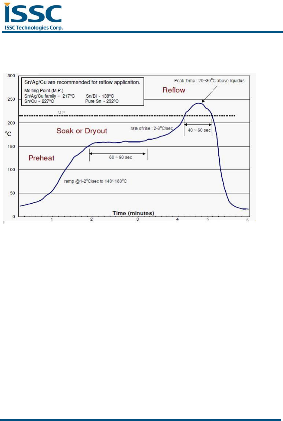
Reflow profile

BM63SPKA1MGA
ISSC Confidential (Version: 1.2) - 25 - 10/15/2014
QR code label information
Label Size:15±1.5 *6±1.5 mm
Device Name: BM63SPKA1MGA
MAC ID: xxxxxxxxxx
Customer ID Name: Cxxxxx
Date Code: 13xx
Module Weight
(Test condition: module with QR label)
TBD

BM63SPKA1MGA
ISSC Confidential (Version: 1.2) - 26 - 10/15/2014
Storage standard
1. Calculated shelf life in sealed bag: 12 months at < 40 ℃ and <90% relative humidity (RH)
2. After bag is opened, devices that will be subjected to reflow solder or other high temperature process
must be Mounted within 168 hours of factory conditions <30℃/60% RH

BM63SPKA1MGA
ISSC Confidential (Version: 1.2) - 27 - 10/15/2014
Ordering Information
Device
Module
Order Number
Size
Shipment
Method
BM63SPKA1MGA
Bluetooth 3.0
digital audio Module
32*15 mm2
Tray
Note:
Minimum Order Quantity is 630pcs Tray.
BM63SPKA1MGA
ISSC Confidential (Version: 1.2) - 28 - 10/15/2014
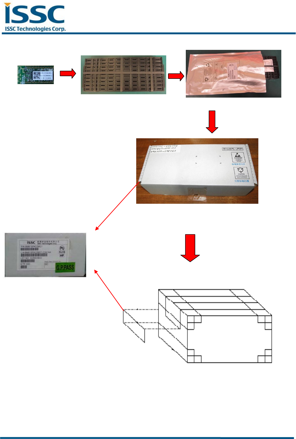
Packing Information
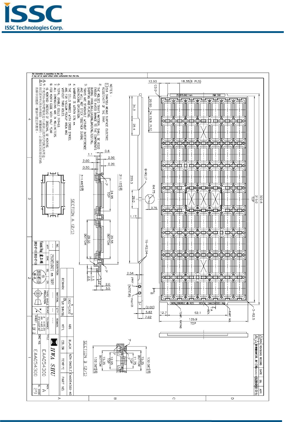
Tray Dimensions
Packing Method
BM63SPKA1MGA
ISSC Confidential (Version: 1.2) - 29 - 10/15/2014
Inner box: Q’ty (630 Pcs)
Dimensions: 36*16*9.5 cm
Bar Code Label
P/N: Device name
C/N: Customer name
Lot No: Lot ID
Q’ty: Box or Carton Module’s Q’ty
Carton: Q’ty (3780 Pcs)
Dimensions: 38*35*30 cm
++=
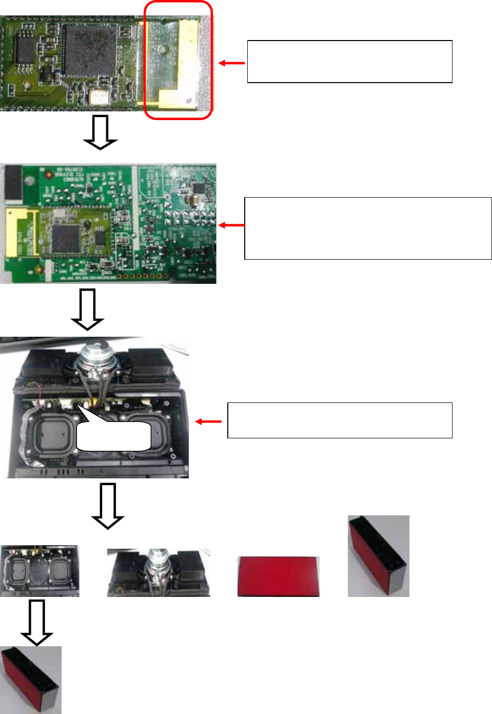
1. BM63modulecontainPCBantenna
2. ThegainofPCBantennais2.4dBi
1. Everymodulehas48pin
2. FixBTmoduleonmainboardbyits8pin
3. Everypinisfixedonthemainboardbytin
Mainboard
1.Mainboardplugintheplasticencloseinside.
SRS‐X55

FCC statement
This device complies with Part 15 of the FCC Rules. Operation is subject to the
following two conditions:
(1) this device may not cause harmful interference, and (2)this device must
accept any interference received, including interference that may cause
undesired operation.
IC statement
This device complies with Industry
Canada licence-exempt RSS standard(s). Operation is subject to the following
two conditions:
(1) this device may not cause interference, and (2) this device
must accept any interference, including interference that may cause undesired
operation of the device
Le présent appareil est conforme aux CNR
d'Industrie Canada applicables aux appareils radio exempts de licence.
L'exploitation est autorisée aux deux conditions suivantes : (1) l'appareil ne doit
pas produire de brouillage, et (2) l'utilisateur de l'appareil doit accepter tout
brouillage radioélectrique subi, même si le brouillage est susceptible d'en
compromettre le fonctionnement.