TCL Technoly Electronics 10 WIFI+BT Audio Module User Manual
TCL Technoly Electronics (Huizhou) Co., Ltd. WIFI+BT Audio Module
User manual

WIFI+BT Audio Module
Model No.型号:TWM-A8516+MT6630T
版本Ve r s i o n :V1.2
公布日期Release Date: 2017-11-28
TONLY ELECTRONICS HOLDINGS LIMITED.通力电子控股有限公司
Address:Section 37, Zhongkai Hi-tech Development Zone, Huizhou Guangdong 516006, P.R.China
地址:中国广东省惠州市仲恺高新区惠风6 路37 号小区网
址http://www.tonlyele.com
©2015 TONLY ELECTRONICS HOLDINGS LIMITED.All rights reserved 保留所有版权

法律声明Legal Notice, Disclaimer, Copyright
本手册是通力电子控股有限公司机密,未经能力电子控股有限公司的事先书面许可,任何人不得复制、
传播本手册的内容。通力电子控股有限公司不对由于使用本手册或执行本手册内容带来的损害负责。
本手册所涉及的知识产权归通力电子控股有限公司所有(或经合作商授权许可使用),任何人不得侵
犯。
本手册是按当前状态提供参考,本公司司保留随时更新本手册的权利,恕不另行通知。本手册不对包括
但不限于下列事项担保:适销性、特殊用途的适应性;实施该用途不会侵犯第三方的知
识产权等权利。本文档在此未以禁止反言或其它方式授予任何知识产权使用许可,不管是明示许可还是暗
示许可。
本手册中提到的所有商标名称、商标和注册商标均属其各自所有者的财产,特此声明.
本协议以中、英文两种语言制作,两种语言文本冲突时,任何时候均以中文为准。
This data sheet contains information that is confidential to TONLY ELECTRONICS HOLDINGS
LIMITED. Unauthorized use or disclosure of the information contained herein is prohibited. You may be held
responsible for any loss or damages suffered by TONLY ELECTRONICS HOLDINGS LIMITED .for your
unauthorized disclosure hereof, in whole or in part.
Information herein is subject to change without noticed. TONLY ELECTRONICS HOLDINGS LIMITED does
not assume any responsibility for any use of, or reliance on, the information contained herein
THIS DATA SHEET AND ALL INFORMATION CONTAINED HEREIN IS PROVIDED “AS IS” WITHOUT
WARRANTY OF ANY KIND, WHETHER EXPRESS, IMPLIED, STATUTORY, OR OTHERWISE. TONLY
ELECTRONICS HOLDINGS LIMITED. SPECIFICALLY DISCLAIMS ALL IMPLIED WARRANTIES OF
MERCHANTABILITY, NON-INFRINGEMENT, AND FITNESS FOR A PARTICULAR PURPOSE. NEITHER
DOES TONLY ELECTRONICS HOLDINGS LIMITED. PROVIDE ANY WARRANTY WHATSOEVER
WITH RESPECT TO THE SOFTWARE OF ANY THIRD PARTY WHICH MAY BE USED BY,
INCORPORATED IN, OR SUPPLIED WITH THIS DATA SHEET, AND USER AGREES TO LOOK ONLY TO
SUCH THIRD PARTY FOR ANY WARRANTY CLAIM RELATING THERETO. TONLY ELECTRONICS
HOLDINGS LIMITED. SHALL ALSO NOT BE RESPONSIBLE FOR ANY TONLY ELECTRONICS
HOLDINGS LIMITED DELIBERABLES MADE TO USER’S SPECIFICATION OR TO CONFORM TO A
PARTICULAR STANDARD OR OPEN FORUM.
Tonlyis a trademark of TONLY ELECTRONICS HOLDINGS LIMITED. other names mentioned in this document
are trademarks/registered trademark of their respective owners.
This data shall be executed in two languages including one Chinese and one English. Any conflict exist between
the two languages, theChinese will prevail in any time.
Smar
t
Voice Assistan
t
Device Module
版本变更说明Document Revision History
Revision
版本
Date
日期
Author
作者
Checkedby
审核
Description
描述
V1.0 2017-10-18 Tommy.li JianliLiang Firstrelease.
V1.1 2017-12-26 Tommy.li JianliLiang
1.GPIODefine;IOPowerDomain
adding.
ThesemodifyarelimitedtoA,D
versionPCB.
V1.2 2018-01-10 Tommy.li JianliLiang 1.USBDM1,DP1,LCMRST,DSITE
Delete;
2.AD1,AD2,AD3,Micbias
Portadding;
Thesemodify arelimited toD
versionPCB.
V1.3 2018-03-29 Tommy.li JianliLiang 1. ModulePin46function
modify:GPI0117GPIO73
2. Pin26,43,42,44Redefinepin
name.
3 TONLYELECTRONICSHOLDINGSLIMITEDConfidential

目录Table of Contents
法律声明Legal Notice, Disclaimer, Copyright
文档变更说明Document Revision History
目录Table of contents
1.系统概览System overview
1.1 通用说明 General Descriptions
1.2 性能特点Features
1.3 系统方框图Block Diagram
2.产品描述Production Description
引脚与功能说明Pin Layout & Pin Description
外观与尺寸 Appearance& Dimension
3.应用说明Application Explanation
4.电气特性Electrical Characteristics
工作条件

5
T
ONL
Y
ELECT
R
ONICS HOLDINGS LIMITED Confidential
直流特性DC characteristics
热特性Thermal characteristics
电流消耗Current consumption
5.射频性能RF Performance
6.认证与法规信息Certificate& Regulation
7.包装与订货说明 Package& Ordering information
8.环保声明Green Policy
9 推荐过炉温度 RECOMMENDED TEMPERATURE REFLOW PROFILE
10.抗静电保护ESDProtection
1. 系统概览System overview
通用说明 General Descriptions
WIFI+BT Audio Mod , The highly integrated module makes the possibilities of web browsing,
VoIP, Bluetooth applications. With seamless roaming capabilities and advanced security, also
could interact with different vendors’
802.11a/b/g/n Access Points in the wireless LAN. This compact module is a total solution for a
combination of WiFi and Bluetooth V4.1technologies.
性能特点Features
Supports 20/40 Mhz at 2.4GHZ and 5GHz
Supports Bluetooth V4.1+HS, BLE and be backwards compatible with Bluetooth 2.1+
enhance data rate.
Supports WLAN-Bluetooth coexistence and ISM-LTE coexistence.
Supports Bluetooth for class1 and class2 power level transmissions without requiring an
external PA.
Audio Interfaces: I2S
support microphone inputs ( PDM digital microphone)
Serial Interfaces: UART, SPI,I2C,USB
Integrated PMU supports multiple low energy States
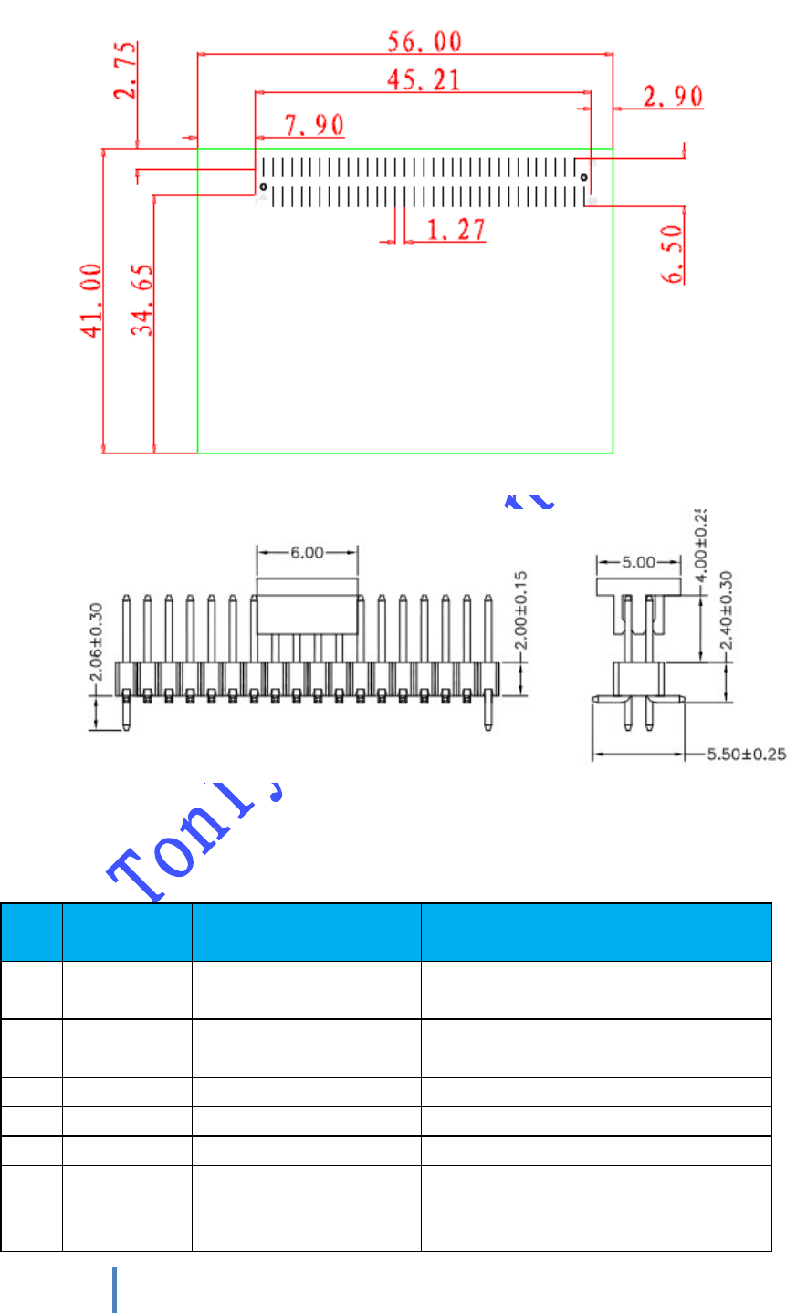
Dimension: 56mm (L) × 41mm (W) ×2.54mm (H)
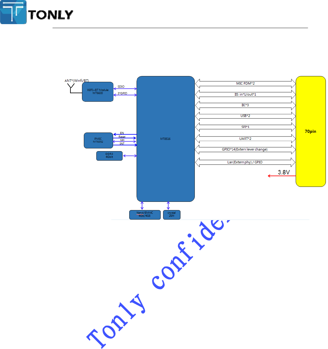
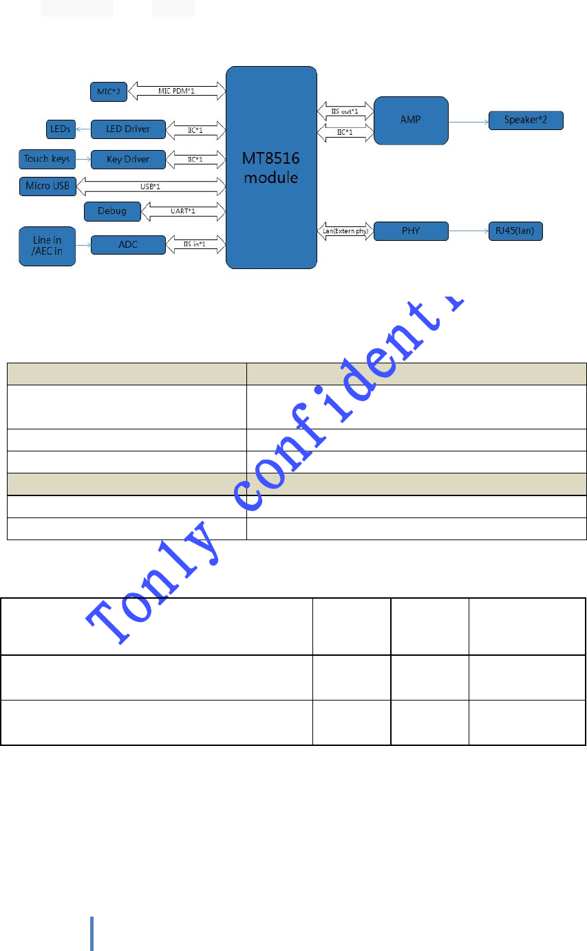
系统方框图 Module Block Diagram
2.产品描述ProductionDescription
引脚与功能说明Apperance&PinDescription& PhysicalDimensions
Description & Apperance :
Smar
t
Voice Assistan
t
Device Module
7
T
ONL
Y
ELECT
R
ONICS HOLDINGS LIMITED Confidential
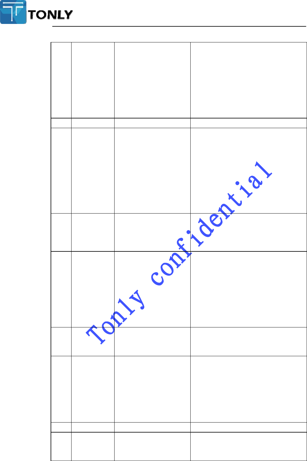
Physical Dimensions
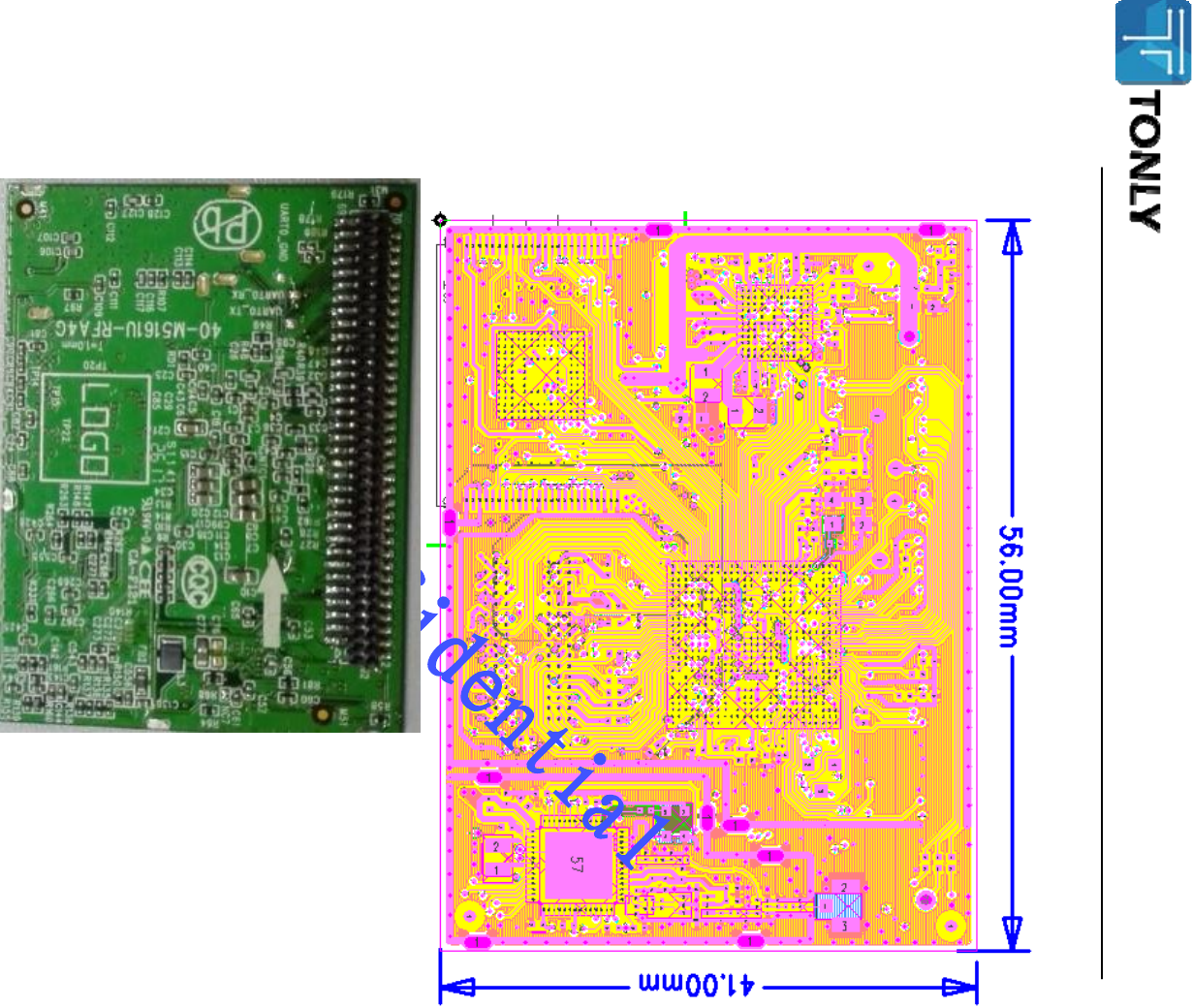
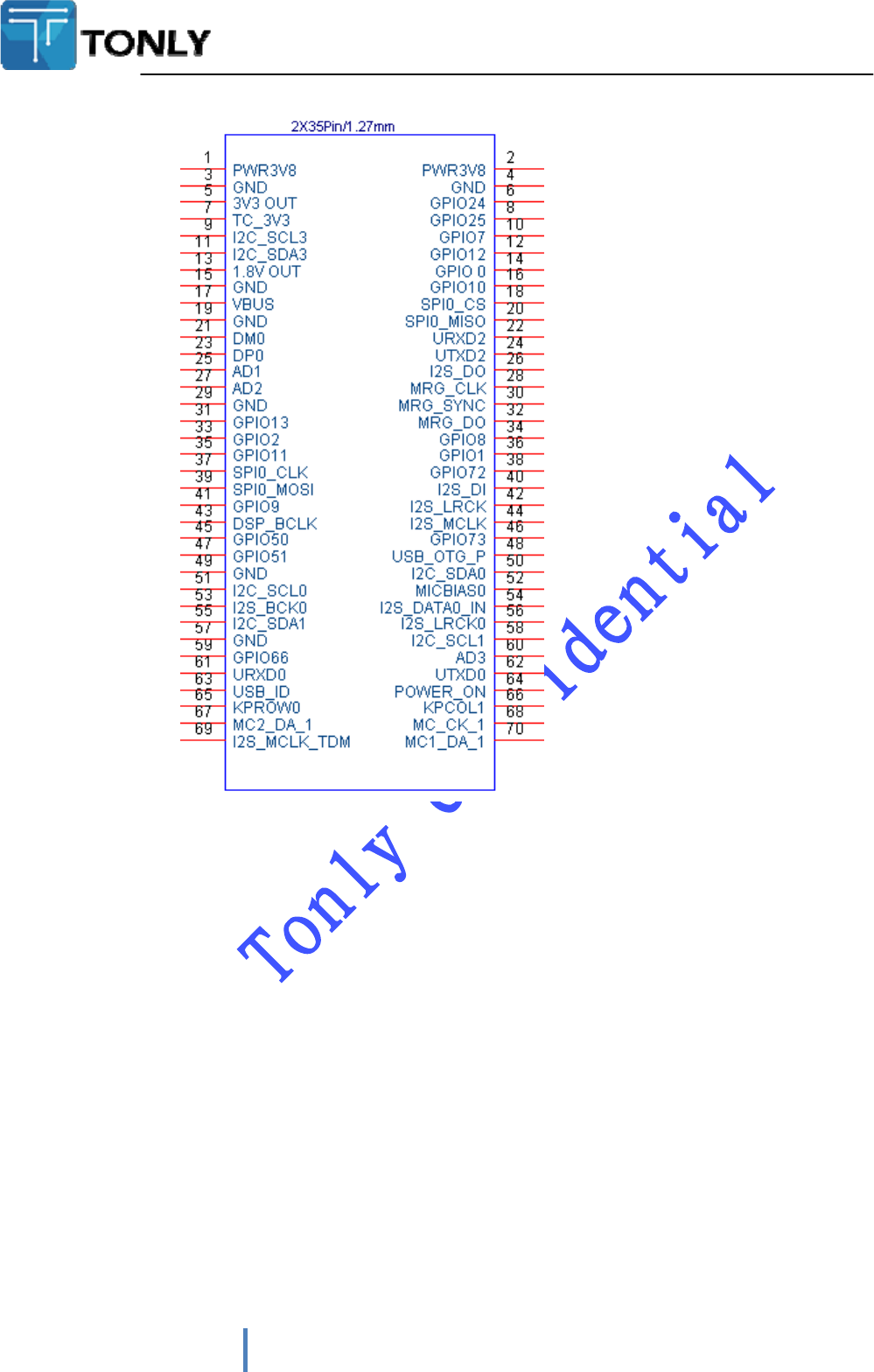
Pin header information
9
T
ONL
Y
ELECT
R
ONICS HOLDINGS LIMITED Confidential
Pindescriptions
PIN
NO.
Symbol
Description Function
1
PWR3V8
Power input VCC input, typical voltage
range :3.6V ~ 4.2V
2
PWR3V8
Power input VCC input, typical voltage
range :3.6V ~ 4.2V
3 GND ground Ground
4 GND ground Ground
5 DSP_3V3 Power output 3.3V power supply
6
GPIO24
Bi-directional with 3.3V
Power domain
GPIO24
Func_DPI_20;
Func_DPI_DE
Func_ANT_SEL1;
Func_UCTS2;
Func_PWM_A;
Func_I2S_MCK;
Func_DBG_Mon-A-O
7 TC_3V3 Power output 3.3V power supply
8
GPIO25
Bi-directional
Power domain
with
3.3V
FUNC_GPIO25.
Func_I2S_8CH_MCK;
Func_ I2S_MCK;
Func_DBG_Mon -A-1;
Func_PWM_B;
Func_URTS2;
Func_ANT_SEL0;
Func_DPI_VSYNC;Func_DPI_D19
9
I2C_SCL3
Bi-directional
Power domain
with
1.8V
Func_I2C SCL2_0;
GPIO61.
Func_PWM_C
10
GPIO7
Bi-directional
Power domain
with
3.3V
FUNC_GPIO7;
Func_SQI RST;
Func_DPI_D6;
Func_SDA1_0;
Func_EXT_RXDV;
Func_CONN_MCU_TMS;
FUNC_CON_MCU_AICE_JMSC;
FUNC_DBG_MON_A_13
11
I2C_SDA3
Bi-directional
Power domain
with 1.8V FUNC_SDA2_0
GPIO60
FUNC_PWM_B
12
GPIO12
Bi-directional
Power domain
with
3.3V
FUNC_GPIO12;
FUNC_CLKM5;FUNC_PWM_A;
FUNC_SPDIF_OUT;
FUNC_ANT_SEL4;
FUNC_DPI_D11;
FUNC_EXT_TXEN;FUNC_DBG_M
ON_A_18.
13 1.8V OUT Power output 1.8V power supply
14
GPIO0
Bi-directional
Power domain
with 3.3V FUNC_GPIO 0
FUNC_PWM_B;
FUNC_DPI_CK;
11
T
ONL
Y
ELECT
R
ONICS HOLDINGS LIMITED Confidential
FUNC_I2S2_BCK;
FUNC_EXT_TXD0;
FUNC_SQICS;
FUNC_DBG_MON_A_6
15 GND ground Ground
16
GPIO10
Bi-directional with 3.3V
Power domain
FUNC_GPIO10
FUNC_CLKM5
FUNC_SCL2_0
FUNC_EXT_FRAME_SYNC
FUNC_EXT_RXD2
FUNC_ANT_SEL2
FUNC_DPI_D9
FUNC_DBG_MON_A_16
17 VBUS Power input USB +5V input
18
SPI0_CS
Bi-directional with 3.3V
Power domain
FUNC_SPI_CSB
FUNC_GPIO5
FUNC_UCTS2
FUNC_DPI_D16
FUNC_EXT_RXER
FUNC_CONN_MCU_TDI
FUNC_CONN_TEST_CK
FUNC_DBG_MON_A_11
19 AGND ground Ground
20
SPI0_MISO
Bi-directional with 3.3V
Power domain
FUNC_GPIO 3;
FUNC_CLKM1;
FUNC_DPI_D14;
FUNC_SPI_MI;
FUNC_EXT_TXD3;
FUNC_CONN_MCU_DBGI_N;
FUNC_SQIWP;
FUNC_DBG_MON_A_9
21 DM0 Bi-directional USB data minus.
22
URXD2
Bi-directional with 3.3V
Power domain
FUNC_URXD2;
FUNC_GPIO 34
FUNC_DPI_D5
FUNC_UTXD2
URXD2__FUNC_DBG_SCL
FUNC_I2S2_MCK
FUNC_DBG_MON_B_0
23 DP0 Bi-directional USB data plus
24
UTXD2 Bi-directional with 3.3V
Power domain
FUNC_UTXD2;
FUNC_GPIO 35;
FUNC_DPI_HSYNC;
FUNC_URXD2;
FUNC_DBG_SDA;
FUNC_DPI_D18;
FUNC_I2S3_MCK;
FUNC_DBG_MON_B_1。
25
AD1
Bi-directional
Aux adc external input channel2
power level full scale is 1.45V.
26
I2S_DO
Bi-directional with 3.3V
Power domain
FUNC_ GPIO 38;
FUNC_MRG_DI
FUNC_DPI_D1
FUNC_I2S0_DI
FUNC_I2S3_DO
FUNC_PCM0_DI
FUNC_EXT_MDIO
FUNC_DBG_MON_A_4
27
AD2
Bi-directional
Aux adc external input channel3
power level full scale is 1.45V.
28
MRG_CLK
Bi-directional with 3.3V
Power domain
FUNC_MRG_CLK
FUNC_GPIO36
FUNC_DPI_D4
FUNC_I2S0_BCK
FUNC_I2S3_BCK
FUNC_PCM0_CLK
FUNC_IR
FUNC_DBG_MON_A_2
29 GND ground Ground
30
MRG_SYNC
Bi-directional with 3.3V
Power domain
FUNC_MRG_SYNC;
FUNC_GPIO37;
FUNC_DPI_D3;
FUNC_I2S0_LRCK
FUNC_I2S3_LRCK
FUNC_PCM0_SYNC
FUNC_EXT_COL
FUNC_DBG_MON_A_3
31
GPIO13
Bi-directional with 3.3V
Power domain
FUNC_GPIO13
FUNC_TSF_IN;
FUNC_ANT_SEL5;
FUNC_DPI_D0;
FUNC_SPDIF_IN;
FUNC_DBG_MON_A_19.
32
MRG_DO
Bi-directional with 3.3V
Power domain
FUNC_MRG_DO
FUNC_GPIO39
FUNC_DPI_D2
13
T
ONL
Y
ELECT
R
ONICS HOLDINGS LIMITED Confidential
FUNC_I2S0_MCK
FUNC_I2S3_MCK
FUNC_PCM0_DO
FUNC_EXT_MDC
FUNC_DBG_MON_A_5
33
GPIO2
Bi-directional with 3.3V
Power domain
FUNC_GPIO2
FUNC_CLKM0;
FUNC_DPI_D13;
FUNC_I2S2_LRCK;
FUNC_EXT_TXD2
FUNC_CONN_MCU_DBGACK_N;
FUNC_SQISI;
FUNC_DBG_MON_A_8
34
GPIO8
Bi-directional with 3.3V
Power domain
FUNC_GPIO8;
FUNC_SQICK;
FUNC_CLKM3;
FUNC_SCL1_0;
FUNC_EXT_RXD0;
FUNC_ANT_SEL0;
FUNC_DPI_D7;
FUNC_DBG_MON_A_14.
35
GPIO11
Bi-directional with 3.3V
Power domain
FUNC_ GPIO11;
FUNC_PWM_C;
FUNC_ANT_SEL3;
FUNC_CLKM4.
36
GPIO1
Bi-directional with 3.3V
Power domain
FUNC_GPIO1 ;
FUNC_PWM_C;
FUNC_DPI_D12;
FUNC_I2S2_DI;
FUNC_EXT_TXD1;
FUNC_CONN_MCU_TDO;
FUNC_SQISO;
FUNC_DBG_MON_A_7
37
SPI0_CLK
Bi-directional with
3.3V Power domain
FUNC_SPI0-CLK;
FUNC_GPIO6.
FUNC_DBG_MON_A_12
38
GPIO72
Bi-directional
wit
h 3.3V Power domain
FUNC_GPIO72;
FUNC_MSDC2_DAT2;
FUNC_I2S_8CH_LRCK;
FUNC_DPI_D23;
FUNC_PWM_C;
FUNC_DBG_MON_B_19
39
SPI0_MOSI Bi-directional with 3.3V
Power domain
FUNC_SP0_MOSI;
FUNC_GPIO4.
40
I2S_DI
Bi-directional
wit
h 3.3V Power domain
FUNC_I2S3_DO;
FUNC_GPIO70;
FUNC_MSDC2_DAT0;
FUNC_I2S_8CH_DO2;
FUNC_DPI_D22;
FUNC_UTXD0;
FUNC_DBG_MON_B_17
41
GPIO9
Bi-directional with 3.3V
Power domain
FUNC_GPIO9
FUNC_CLKM4;
FUNC_SDA2_0;
FUNC_EXT_FRAME_SYNC;
FUNC_EXT_RXD1;
FUNC_ANT_SEL1;
FUNC_DPI_D8;
FUNC_DBG_MON_A_15.
42
I2S_LRCK
Bi-directional with 3.3V
Power domain
FUNC_I2S3_LRCK;
FUNC_GPIO69;
FUNC_MSDC2_CLK;
FUNC_I2S_8CH_DO3;
FUNC_SCL1_0;
FUNC_DPI_D21;
FUNC_USB_SCL;
FUNC_I2S3_LRCK;
FUNC_DBG_MON_B_16
43
I2S_BCLK
Bi-directional with 3.3V
Power domain
FUNC_I2S3_BCK;
FUNC_GPIO68;
FUNC_MSDC2_CMD;
FUNC_I2S_8CH_DO4;
FUNC_SDA1_0;
FUNC_USB_SDA;
FUNC_I2S3_BCK;
FUNC_DBG_MON_B_15.
44
I2S_MCLK
Bi-directional with 3.3V
Power domain
FUNC_I2S3_MCK;
FUNC_GPIO71;
FUNC_MSDC2_DAT1;
FUNC_I2S_8CH_DO1;
FUNC_PWM_A;
FUNC_I2S3_MCK;
FUNC_URXD0;
FUNC_PWM_B;
FUNC_DBG_MON_B_18.
15
T
ONL
Y
ELECT
R
ONICS HOLDINGS LIMITED Confidential
45
GPIO50 Bi-directional with 1.8V
Power domain
FUNC_SPI_MISO
FUNC_GPIO50
46
GPIO73
Bi-directional with 3.3V
Power domain
FUNC_I2S_8CH_BCK
FUNC_GPIO73
FUNC_PWM_A
47 GPIO51 Bi-directional with 1.8V
Power domain
FUNC_SPI_MOSI
FUNC_GPIO51
48
USB_OTG_P
WR_EN
Bi-directional with 1.8V
Power domain
FUNC_GPIO49 For
USB_OTG_PWR_EN
FUNC_SPI_CK
49 GND ground Ground
50
I2C_SDA0 Bi-directional with 1.8V
Power domain
FUNC_SDA0_0;
FUNC_GPIO58.
51
I2C_SCL0 Bi-directional with 1.8V
Power domain
I2C SCL0;
FUNC_GPIO59.
52 MICBIAS0 Power output Microphone bias A
53
I2S_BCK0
Bi-directional with 1.8V
Power domain
FUNC_I2S0_BCK;
FUNC_GPIO57;
FUNC_URTS0;
FUNC_I2S3_BCK;
FUNC_I2S_8CH_BCK;
FUNC_PWM_C;
FUNC_I2S2_LRCK;
FUNC_DBG_MON_A_30
54
I2S_DATA0_
IN
Bi-directional with 1.8V
Power domain
FUNC_I2S3_DO;
FUNC_GPIO55;
FUNC_I2S0_DI;
FUNC_UCTS0;
FUNC_I2S_8CH_DO1;
FUNC_PWM_A;
FUNC_I2S2_BCK;
FUNC_DBG_MON_A_28.
55
I2C_SDA1 Bi-directional with 1.8V
Power domain
FUNC_SDA1_0;
FUNC_GPIO52.
56
I2S_LRCK0
Bi-directional with 1.8V
Power domain
FUNC_I2S0_LRCK;
FUNC_GPIO56;
FUNC_I2S3_LRCK;
FUNC_I2S_8CH_LRCK;
FUNC_PWM_B;
FUNC_I2S2_DI;
FUNC_DBG_MON_A_29
57 GND ground Ground
58
I2C_SCL1 Bi-directional with 1.8V
Power domain
FUNC_SCL1_0;
FUNC_GPIO53
59
GPIO66 Bi-directional with 1.8V
Power domain FUNC_I2S0_MCK
60
AD3
Bi-directional
Aux adc external input channel3
power level full scale is 1.45V.
61
URXD0
Bi-directional with 1.8V
Power domain
FUNC_GPIO62;
FUNC_URXD0;
FUNC_UTXD0.
62
UTXD0
Bi-directional with 1.8V
Power domain
FUNC_GPIO63;
FUNC_UTXD0;
FUNC_URXD0
63
USB_ID
Bi-directional with 1.8V
Power domain
FUNC_GPIO41
FUNC_KPROW1;
FUNC_IDDIG;
FUNC_EXT_FRAME_SYNC;
FUNC_MFG_TEST_CK;
FUNC_DBG_MON_B_5.
64
POWER_ON
PWR
Powe
r
Ke
y
, active low.
65
KPROW0
Bi-directional with 1.8V
Power domain
FUNC_KPROW0;
FUNC_GPIO40;
FUNC_IMG_TEST_CK;
FUNC_DBG_MON_B_4.
66
GPIO43
Bi-directional with 1.8V
Power domain
FUNC_GPIO43;
FUNC_KPCOL1;
FUNC_USB_DRVVBUS;
FUNC_EXT_FRAME_SYNC;
FUNC_TSF_IN;
FUNC_DFD_NTRST_XI;
FUNC_UDI_NTRST_XI;
FUNC_DBG_MON_B_7;
67 MC2_DA_1 PDM digital microphone Digital microphone Data2
68 MC_CK_1 PDM digital microphone Digital microphone Clk
69
I2S_MCLK_
TDM
Bi-directional with 1.8V
Power domain
FUNC_TDM_RX_MCK;
FUNC_GPIO100;
FUNC_CMDAT0;
FUNC_CMCSD0;
FUNC_ANT_SEL2;
FUNC_TDM_RX_MCK;
FUNC_DBG_MON_B_21
70 MC1_DA_1 PDM digital microphone Digital microphone Data1
Remark:Boldness is the default function by Tonly’s software.
17
T
ONL
Y
ELECT
R
ONICS HOLDINGS LIMITED Confidential
ELECTRICAL CHARACTERISTICS
Supply Voltage 3.8V DC
(Absolute Maximum Ratings 4.2V)
Working current RMS 300mA
Sleep current 33mA
WEIGHT AND DIMENSIONS (unit : mm)
Size (L x W x H) 56mm (L) × 41mm (W) ×1.6mm (H)
Weight ~8.5g
3.应用说明Application Explanations
All portable Smart devices
3.1 Application Block Diagram
4. 电气特性Electrical Characteristics
Base Characteristics
Recommended operating conditions
Recommended operating conditions
Min
Max
Unit
Operatingtemperature -10 60
°C
PWR3V8 3.6 4.2
V
5.射频性能RF Performance
18
T
ONL
Y
ELECT
R
ONICS HOLDINGS LIMITED Confidential
2.4G BT
BR
Parameter Description Typ. Unit
Output power At max power output
level
8 dBm 5.5±4
ICFT Initial carrier frequency
drift
±18 kHz <±75
Carrier frequency
drift
One slot packet (DH1) ±10 kHz <±25
Three slot packet (DH3) ±10 kHz <±40
Five slot packet (DH5) ±10 kHz <±40
Max. drift rate 10 kHz/50u
s
<20
Receiver sensitivity BER < 0.1% -90 dBm
EDR
Parameter Description Typ. Unit
Output power π/4 DQPSK 5 dBm 2.5±4
8PSK 5 dBm 2.5±4
Frequency stability ω0, π/4 DQPSK ±4 kHz <±10
ω0, 8PSK ±4 kHz <±10
ωi, π/4 DQPSK ±18 kHz <±75
ωi, 8PSK ±18 kHz <±75
|ω0+ωi|, π/4 DQPSK ±20 kHz <±75
|ω0+ωi|, 8PSK ±20 kHz <±75
Modulation accuracy RMS DEVM, π/4
DQPSK
8 % <20
RMS DEVM, 8PSK 8 % <13
Peak DEVM, π/4
DQPSK
15 % <35
Peak DEVM, 8PSK 15 % <25
Receiver sensitivity π/4 DQPSK (BER <
0.01%)
-90 dBm
8PSK (BER < 0.01%) -89 dBm
LE
Parameter Description Typ. Unit
Output power(*) At max. power output
level
5.5 dBm 5.5±4
Carrier frequency
offset and drift
Frequency offset ±10 kHz <±150
Frequency drift ±10 kHz <±50
Max. drift rate ±10 kHz/us <±20
Parameter Description Typ. Unit
Receiver sensitivity
(*)
PER < 30.8% -90 dBm
6.认证与法规信息Certification& Regulation
The Certification:
FCC&ICID、RED、SRRC、MICPretestOK.
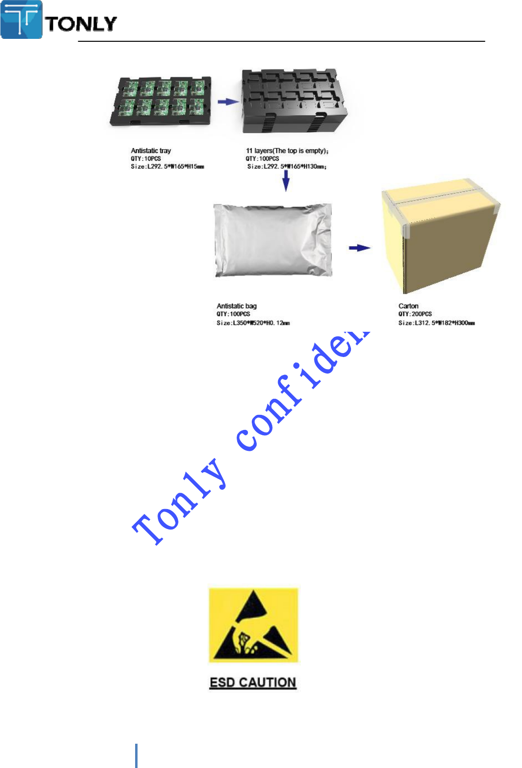
7.包装与订货说明Package & Ordering Information
Assembly Information
Smar
t
Voice Assistan
t
Device Module
8.环保声明Green Policy
This module can meet ROHS&REACH compliance.
9.推荐过炉温度 RECOMMENDED TEMPERATURE REFLOW PROFILE
NC
10.抗静电保护 ESDProtection
TWM-A8516-MT6330TisESD(electrostaticdischarge)sensitivedeviceandmaybe
20 TONLYELECTRONICSHOLDINGSLIMITEDConfidential
The TMW-A8516+MT6630Thas been designed to pass certification with the antenna listed below. The required antenna impedance is 50 ohms.
ModelType Connector
Peakgain(dBi)
2400‐2483.5
MHz
5150‐5250
MHz
5250‐5350
MHz
5470‐5725
MHz
5725‐5850
MHz
N/APIFARF‐SMA3.0dBi6.396.396.396.39
damagedwithESDorspikevoltage.AlthoughTWM-A8516-MT6330Tiswith
built-inESDprotectioncircuits,pleasehandlewithcaretoavoidthepermanent
malfunctionortheperformancedegradation.
FCC Statement
This device complies with part 15 of the FCC rules. Operation is subject to the following two conditions: (1) this device may not cause harmful interference, and (2) this device must
accept any interference received, including interference that may cause undesired operation.
Changes or modifications not expressly approved by the party responsible for compliance could void the user’s authority to operate the equipment.
NOTE: this equipment has been tested and found to comply with the limits for a Class B digital device, pursuant to part 15 of the FCC Rules. These limits are designed to provide
reasonable protection against harmful interference in a residential installation. This equipment generates uses and can radiate radio frequency energy and, if not installed and used in
accordance with the instructions, may cause harmful interference to radio communications. However, there is no guarantee that interference will not occur in a particular installation.
If this equipment does cause harmful interference to radio or television reception, which can be determined by turning the equipment off and on, the user is encouraged to try to
correct the interference by one or more of the following measures:
●
Reorient of relocate the receiving antenna.
●
Increase the separation between the equipment and receiver.
●
Connect the equipment into an outlet on a circuit difference from that to which the receiver is connected.
●
Consult the dealer or an experienced radio/TV technician for help.
Important Note:
Radiation Exposure Statement
This equipment complies with FCC radiation exposure limits set forth for an uncontrolled environment. This equipment should be installed and operated with minimum distance 20
cm between the radiator and your body.
This transmitter must not be co-located or operating in conjunction with any other antenna or transmitter.
Country Code selection feature to be disabled for products marketed to the US/Canada.
1.
The antenna must be installed such that 20 cm is maintained between the antenna and users, and
2.
The transmitter module may not be co-located with any other transmitter or antenna.
As long as the three conditions above are met, further transmitter testing will not be required. However, the OEM integrator is still responsible for testing their end-product for any
additional compliance requirements required with this module installed.
Important Note:
In the event that these conditions cannot be met (for example certain laptop configurations or co-location with another transmitter), then the FCC authorization is no longer
considered valid and the FCC ID cannot be used on the final product. In these circumstances, the OEM integrator will be responsible for re-evaluating the end product (including
the transmitter) and obtaining a separate FCC authorization.
End Product Labeling:
The final end product must be labeled in a visible area with the following “Contains FCC ID: ZVA10”
Manual Information to the End User:
The OEM integrator has to be aware not provide information to the end user regarding how to install or remove this RF module in the user’s manual of the end product which
integrates this module.
The end user manual shall include all required regulatory information/warning as show in this manual.
Antenna information
Antenna information
The TMW-A8516+MT6630T has been designed to pass certification with the antenna listed below. The required antenna
impedance is 50 ohms.
ISED Statement
–
English: This device complies with Industry Canada licenseexempt RSS standard(s). Operation is subject to the
following
two conditions: (1) This device may not cause interference, and (2) This device must accept any interference, including
interference that may cause undesired operation of the device. The digital apparatus complies with Canadian CAN ICES3 (B)/
NMB3 (B).
–
French: Le présentappareilestconforme aux CNR d'Industrie Canada applicables aux appareils
radio exempts de licence. L'exploitationestautorisée aux deux conditions suivantes: (1) l'appareil ne doit pas produire de
brouillage, et (2) l'utilisateur de l'appareildoit accepter tout brouillageradioélectriquesubi, mêmesi le brouillageest susceptible
d'encompromettre le fonctionnement.
This radio transmitter (ISED certification number: 9976A-10) has been approved by Industry Canada to operate with the
maximum permissible gain indicated. Strictly prohibited for use with thisdevice with maximum antenna gain.
Le présentémetteur radio (ISED certification number: 9976A-10) a
étéapprouvée
par industriecanada pour fonctionner
avec le gain maximal indiqué.strictementinterdite pour utilisation avec cedispositif avec le maximum de gain d'antenne.
ModelType Connector
Peakgain(dBi)
2400‐2483.5
MHz
5150‐5250
MHz
5250‐5350
MHz
5470‐5725
MHz
5725‐5850
MHz
N/APIFARF‐SMA3.0dBi6.396.396.396.39
Radiation Exposure Statement
This equipment complies with Canada radiation exposure limits set forth for an uncontrolled environment. This equipment
should be installed and operated with minimum distance 20 cm between the radiator and your body.
Déclarationd'exposition aux radiations
Cetéquipementestconforme Canada limitesd'exposition aux radiations dans un environnement non contr
ô
lé.
Cetéquipementdoitêtreinstallé et utilisé
à
distance minimum de 20cm entre le radiateur et votre corps.
This device is intended only for OEM integrators under the following condition:
The transmitter module may not be co-located with any other transmitter or antenna.
As long as the condition above is met, further transmitter test will not be required. However, the OEM integrator is still
responsible for testing their end-product for any additional compliance requirements required with this module installed.
Cetappareilestcon
ç
uuniquement pour les intégrateurs OEM dans les conditions suivantes:
Le module émetteurpeut ne pas êtreco
ï
mplanté avec unautreémetteurouantenne.
Tant que les 1 condition ci-dessussontremplies, des essaissupplémentaires sur l'émetteur ne seront pas nécessaires.
Toutefois, l'intégrateur OEM esttoujoursresponsable des essais sur son produit final pour toutesexigences de
conformitésupplémentairesrequis pour ce module installé.
Important Note:
In the event that these conditions cannot be met (for example certain laptop configurations or co-location with another
transmitter), then the Canada authorization is no longer considered valid and the IC cannot be used on the final product.
In these circumstances, the OEM integrator will be responsible for re-evaluating the end product (including the
transmitter) and obtaining a separate Canada authorization.
The en
d
use
r
manual shall include all require
d
regulatory information/warning as show in this manual.
Manuel d'information à l'utilisateur final
Note Importante:
Dans le casoùces conditions ne peuventêtresatisfaites (par exemple pour certaines configurations d'ordinateur
portable ou de certaines co-localisation avec un autreémetteur), l'autorisation du Canada n'est plus
considérécommevalide et l' IC ne peut pas êtreutilisé sur le produit final. Danscescirconstances, l'intégrateur
OEM sera chargé de réévaluer le produit final (y comprisl'émetteur) etl'obtentiond'uneautorisationdistincte au
Canada.
End Product Labeling
The final end product must be labeled in a visible area with the following: Contains IC:9976A-10.
Plaque signalétique du produit final
Le produit final doitêtreétiquetédansunendroit visible avec l'inscriptionsuivante: Contient des IC:9976A-10.
Manual Information to the End User
The OEM integrator has to be aware not to provide information to the end user regarding how to install or remove this RF module
in the user’s manual of the end product which integrates this module.
Caution:
(i) Thedeviceforoperationintheband5150–5250MHzisonlyforindoorusetoreducethepotentialforharmfulinterference
toco‐channelmobilesatellitesystems;
(ii) Fordeviceswithdetachableantenna(s),themaximumantennagainpermittedfordevicesinthebands5250‐5350MHzand
5470‐5725MHzshallbesuchthattheequipmentstillcomplieswiththeEIRPlimit;
(iii) Fordeviceswithdetachableantenna(s),themaximumantennagainpermittedfordevicesintheband5725‐5850MHzshall
besuchthattheequipmentstillcomplieswiththeEIRPlimitsspecifiedforpoint‐to‐pointandnon‐point‐to‐pointoperation
asappropriate;andoperationsinthe5.25‐5.35GHzbandarerestrictedtoindoorusageonly.
Avertissement:
(i) lesdispositifsfonctionnantdanslabandede5150à5250MHzsontréservésuniquementpouruneutilisationàl'intérieurafin
deréduirelesrisquesdebrouillagepréjudiciableauxsystèmesdesatellitesmobilesutilisantlesmêmescanaux;
(ii) pourlesdispositifsmunisd'antennesamovibles,legainmaximald'antennepermispourlesdispositifsutilisantlesbandesde
5250à5350MHzetde5470à5725MHzdoitêtreconformeàlalimitedelap.i.r.e;
(iii) pourlesdispositifsmunisd'antennesamovibles,legainmaximald'antennepermis(pourlesdispositifsutilisantlabandede
5725à5850MHz)doitêtreconformeàlalimitedelap.i.r.e.spécifiéepourl'exploitationpointàpointetl'exploitationnon
pointàpoint,selonlecas;Lesopérationsdanslabandede5.25‐5.35GHzsontlimitésàunusageintérieurseulement.
-------------------------END--------------------------