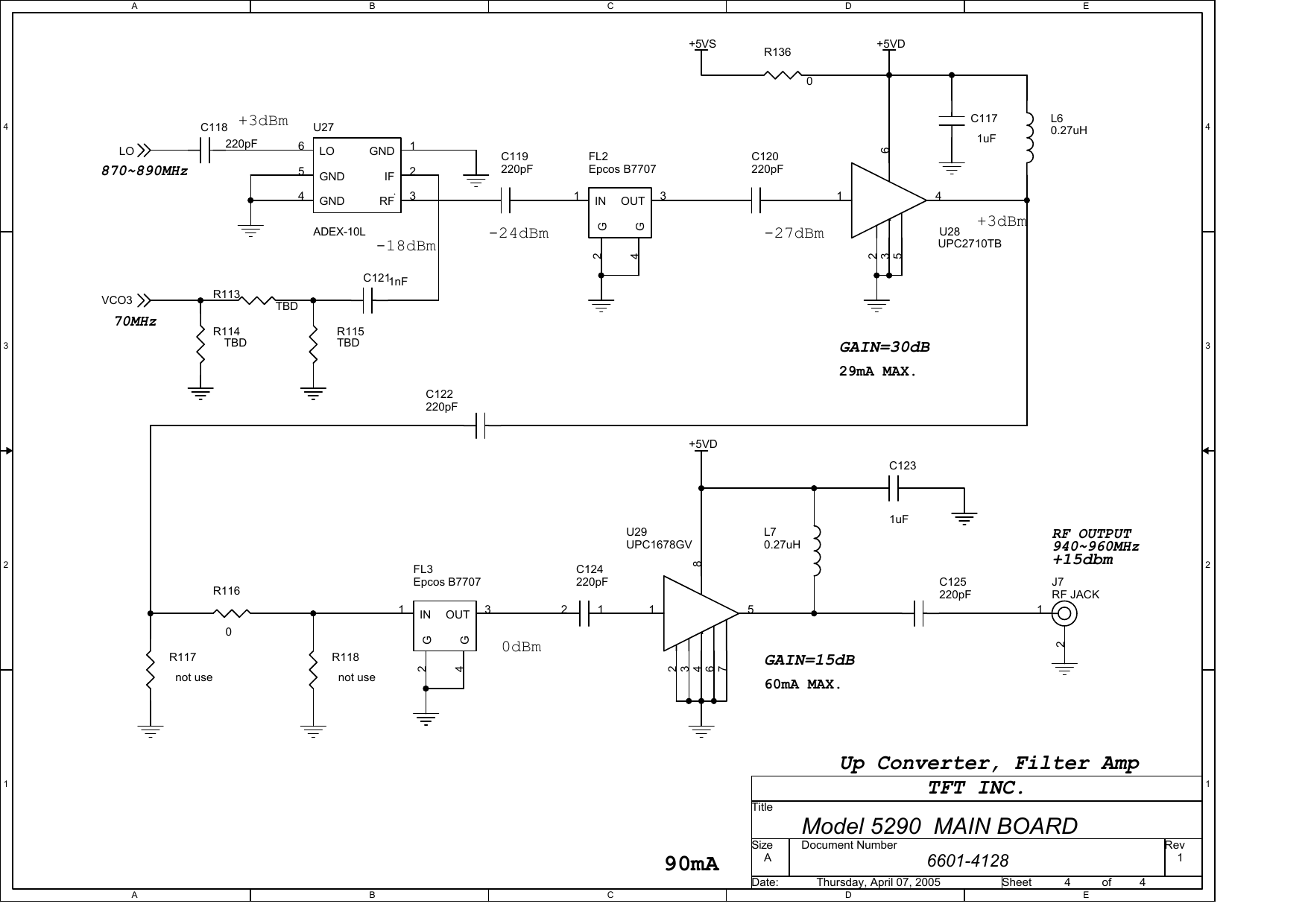
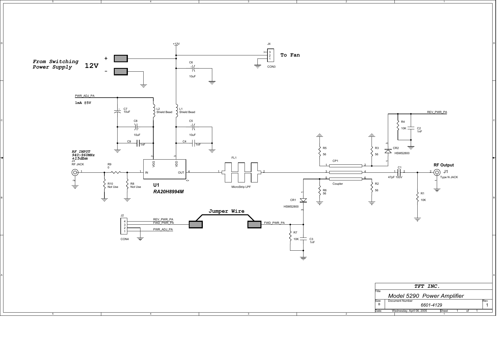
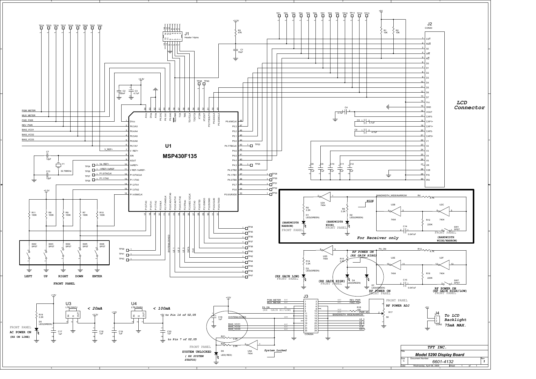
TFT 5290 ANALOG STUDIO TO TRANSMITTER LINK User Manual TITLE PAGE
TFT Inc ANALOG STUDIO TO TRANSMITTER LINK TITLE PAGE
UserManual.wiki
>
TFT
>
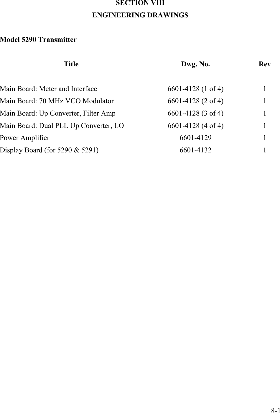
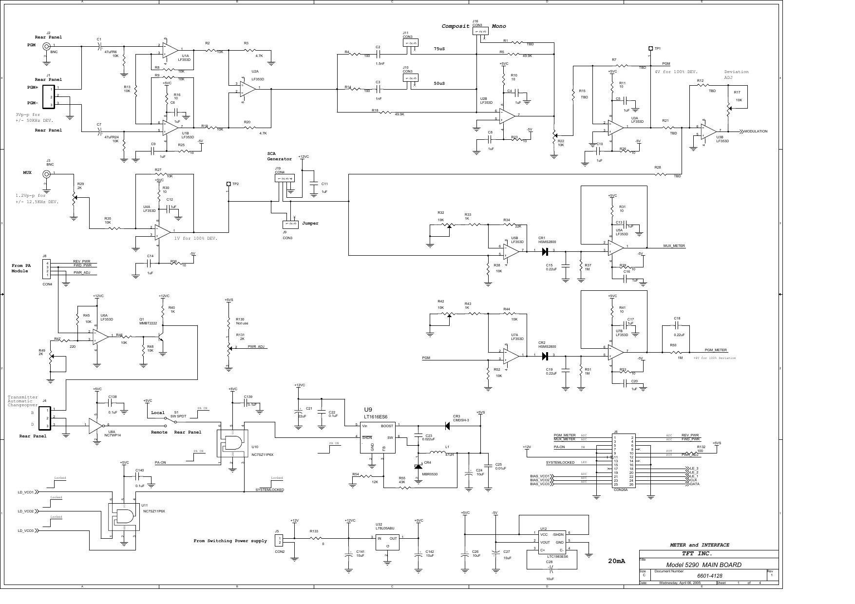
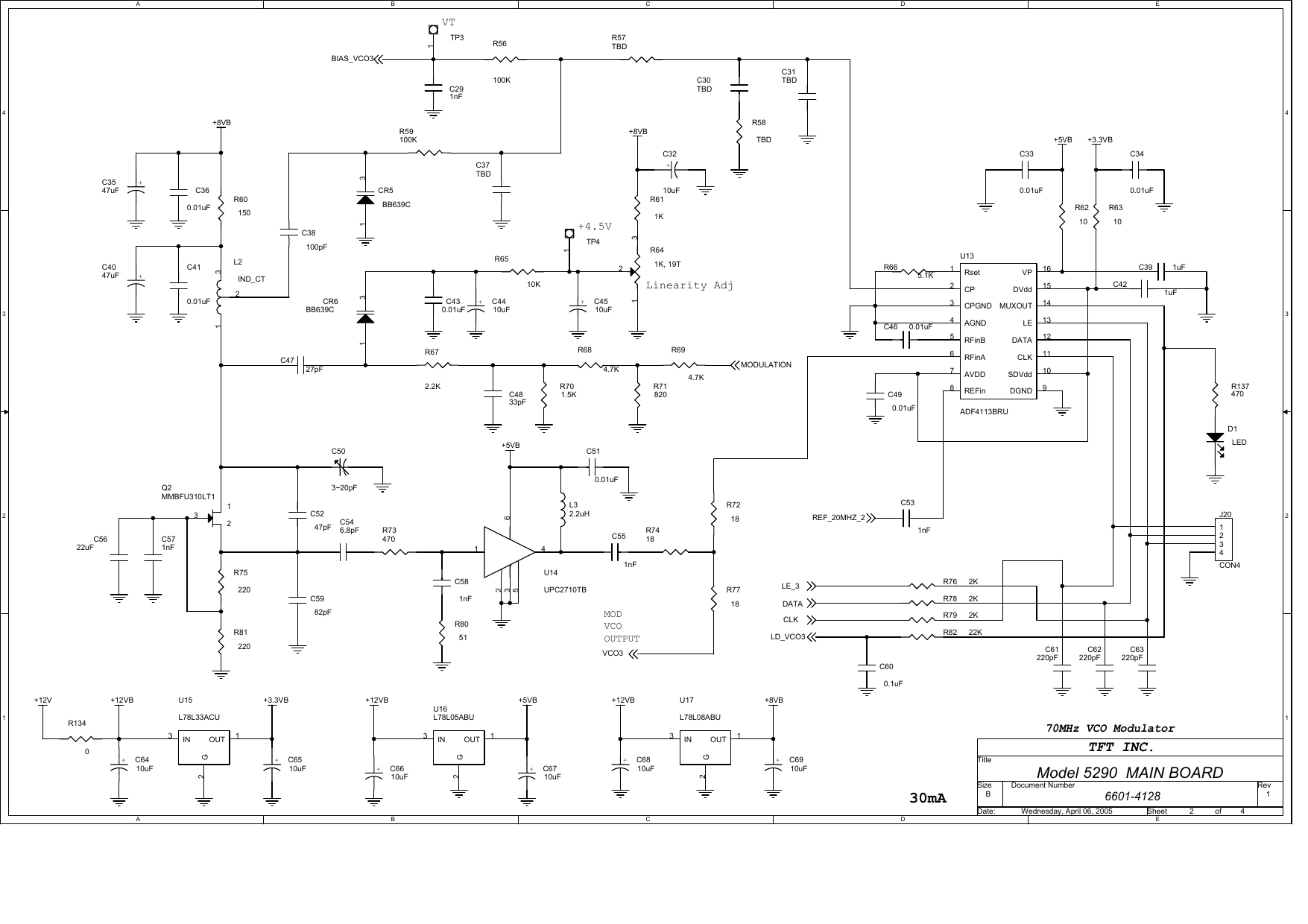
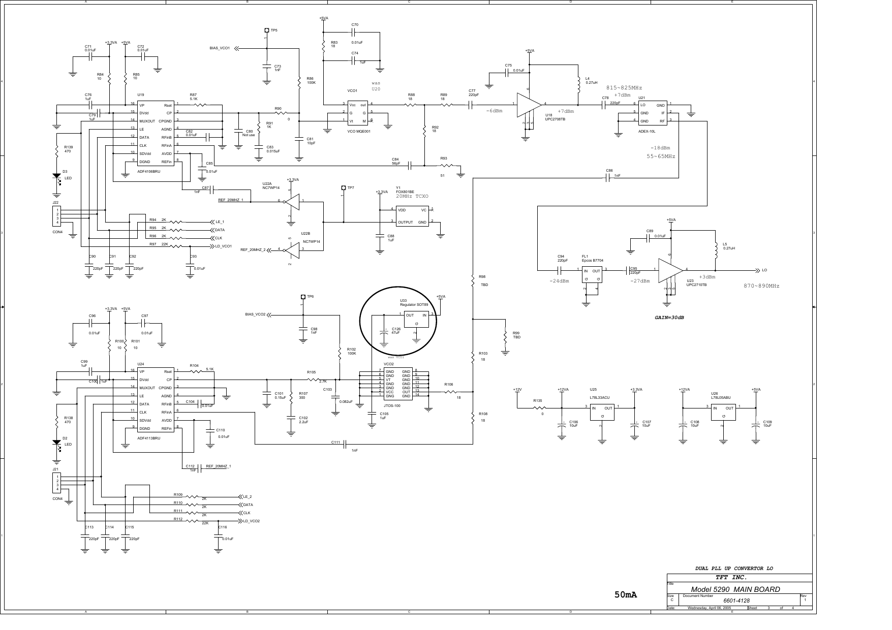
5290 User Manual
manual
Navigation menu
Upload a User Manual
Namespaces
Wiki Guide
HTML
PDF
Info
Views
User Manual
Discussion / Help
Navigation