TFT 5290 ANALOG STUDIO TO TRANSMITTER LINK User Manual TITLE PAGE
TFT Inc ANALOG STUDIO TO TRANSMITTER LINK TITLE PAGE
TFT >
manual

P/N 5004-5200 REV. A (Preliminary)
APRIL 2005
EQUIPMENT SERIAL NO.
SHIPMENT DATE
ANALOG STUDIO TO TRANSMITTER LINK
Model 5290 STL Transmitter
Model 5291 STL Receiver
USER’S GUIDE
Preliminary
1953 Concourse Drive
San Jose, California 95131-1708 USA
TEL: (+1) 408 943-9323
FAX: (+1) 408 943-9218
EMAIL: techsupport@TFTInc.com
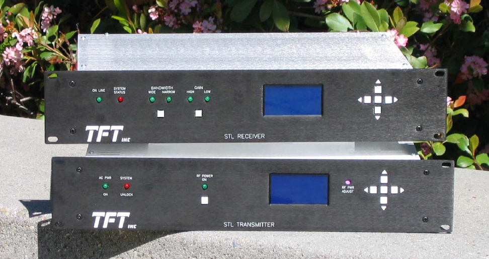
MODEL 5291
STL RECEIVER
MODEL 5290
STL TRANSMITTER
The TFT 5200 Analog STL Series consists of a transmitter and receiver pair that accommodates a
single RF channel. The transmitter is either composite or mono. Receivers are available in
composite/mono, composite only, and monaural only versions. Both the transmitter and receiver are
frequency agile across a specific band and all bands from 140 MHz to 1.7 GHz are available. The
Model 5290 Transmitter covers 944-952 MHz, along with its companion composite/mono receiver,
the Model 5291.
The transmitter has a 20-Watt output and is frequency agile in 6.25 kHz steps, set by front panel
switches.
FEATURES:
• 20 Watts
• Frequency Agile
• Composite or mono, jumper selectable
• Wideband or narrowband
• Frequency Stability 0.0005%
• THD <0.05%
• SNR >80 dB
• Selectable Pre-/De-Emphasis
• 10 µV sensitivity for 60 dB SNR
• 152 kHz MUX available
• Front Panel LCD
• Modulation Bargraph
• Type N RF Connectors
• FCC ID: BIO5290*(Pending)
ii
TABLE OF CONTENTS
Paragraph Title Page
Section I – GENERAL INFORMATION
1.1 INTRODUCTION………………………………………………………………………………... 1-1
1.2 EQUIPMENT DESCRIPTION………………………………………………………………….. 1-1
1.3 SPECIFICATIONS………………………………………………………………………………. 1-2
1.4 FCC DESIGNATOR………………………………………………………….………………….. 1-3
1.5 WARRANTY INFORMATION………………………………………………………………… 1-3
1.6 CLAIMS FOR DAMAGE IN SHIPMENT………………………………….…………………. 1-3
1.7 TECHNICAL SUPPORT………………………………………………………………………... 1-3
Section II – GETTING TO KNOW YOUR SERIES 5200 STL AND RELATED
EQUIPMENT
2.1 INTRODUCTION………………………………………………………………………………
…
2-1
2.2 UNPACKING &
INSPECTION………………………………………………………………….
2-1
2.3 THE 5290 STL TRANSMITTER FRONT
PANEL……………………………………………..
2-1
2.4 THE 5290 STL TRANSMITTER REAR
PANEL……………………………………….……...
2-2
2.5 THE 5291 STL RECEIVER FRONT
PANEL………….……………………………………….
2-3
2.6 THE 5291 STL RECEIVER REAR
PANEL…………….………………….…………………...
2-4
2.7 RELATED
EQUIPMENT………………………………………………………………………...
2-4
2.8 PRE-INSTALLATION
INFORMATION……………………………………………………….
2-5
Section III – PRE-INSTALLATION CHECKOUT
3.1 INTRODUCTION………………………………………………………………………………
…
3-1
3.2 PRIMARY POWER 3-1
ii
Paragraph Title Page
APPLICATION……………………………………………………………
iii
Section IV - OPERATING
4.1 INTRODUCTION………………………………………………………………………………... 4-1
4.2 OVERVIEW OF OPERATION………………………………………………………………… 4-1
4.3 SETTING TRANSMITTER
PARAMETERS…………………………………………………...
4-1
4.4 OBSERVING TRANSMITTER
OPERATING...……………………………………………….
4-1
4.5 SETTING RECEIVER
PARAMETERS…..…………………………………………………….
4-1
Section V – INSTALLATION
5.1 INTRODUCTION………………………………………………………………………………
…
5-1
Section VI – THEORY OF OPERATION
6.1 GENERAL …………………………………………………………………………………….…. 6-1
6.2 MODEL 5290 STL TRANSMITTER BASIC DIAGRAM DESCRIPTION...……………….. 6-1
6.3 MODEL 5291 STL RECEIVER BASIC DIAGRAM
DESCRIPTION..………………………
6-1
Section VII – MAINTENANCE AND REPAIR
7.1 INTRODUCTION………………………………………………………………………………
…
7-1
7.2 TOOL AND TEST EQUIPMENT
REQUIREMENTS…………………….…………………...
7-1
7.3 ROUTINE
MAINTENANCE……………………………………………………………………..
7-1
7.3.1
Calibration……………………………………………………………………………………...
7-1
7.4 DIAGNOSTICS AND
REPAIR…………………………………………………………………..
7-1
7.5 TFT CUSTOMER SERVICE
DEPARTMENT…………………………………………………
7-1
iv
Section VIII – ENGINEERING DRAWINGS
v

vi
List of Figures
Figure Title Page
2.3-1 Model 5290 STL Transmitter Front Panel 2-1
2.4-1 Model 5290 STL Transmitter Rear Panel 2-2
2.5-1 Model 5291 STL Receiver Front Panel 2-3
2.6-1 Model 5291 STL Receiver Rear Panel Connectors 2-4
List of Tables
Table Title Page
1.3-1 Transmitter and Receiver Specifications 1-2
2.3-1 Model 5290 STL Transmitter Front Panel Controls and Indicators 2-1
2.4-1 Model 5290 STL Transmitter Rear Panel Connectors 2-2
2.5-1 Model 5291 STL Receiver Front Panel Indicators and Controls 2-3
2.6-1 Model 5291 STL Receiver Rear Panel Connectors 2-4
SECTION I
GENERAL INFORMATION
1.1 INTRODUCTION
This Model 5200 STL User’s Guide is arranged in seven sections, as follows:
Section I: General Information
A general description of the 5200 Series Transmitter, its specifications, general information on the FCC designator, warranty
and damage claim procedures, and technical support information.
Section II Getting To Know Your Model 5200 Series Transmitter and Receiver and Related Equipment
Overview of the various system components of the 5200 Series Transmitter and Receiver and related equipment. Control and
Indicator functions, basic component functions, and their interconnection.
Section III: Pre-Installation Checkout
Some basic test methodology on the Transmitter and Receiver and their related equipment. The user should find it useful to
perform the tests in this section with all the 5200 Series Transmitter and Receiver equipment on a lab bench.
Section IV: Operating the Transmitter and Receiver
Detailed description of setup procedures of various Transmitter and Receiver system parameters, as well as enabling of
optional features.
Section V: Installation
Instruction for installing and adjusting various system components of the 5200 Series Transmitter and Receiver.
Section VI: Theory of Operation
Basic description of transmitter and receiver circuits
Section VII: Maintenance and Repair
Describes routine maintenance procedures and tools and equipment requirements.
Section VIII: Engineering Drawings
1.2 EQUIPMENT DESCRIPTION
The TFT 5200 Analog STL Series consists of a transmitter and receiver pair that accommodates a
single RF channel. The transmitter is either composite or mono. Receivers are available in
composite/mono, composite only, and monaural only versions. Both the transmitter and receiver are
frequency agile across a specific band and all bands from 140 MHz to 1.7 GHz are available. The
Model 5290 Transmitter covers 944-952 MHz, along with its companion composite/mono receiver,
the Model 5291.
The transmitter has a 20-Watt output and is frequency agile in 6.25 kHz steps, set by front panel
switches.
1-1
1.3 SPECIFICATIONS
The Transmitter and Receiver System Specifications are listed in Table 1.3-1.
Table 1.3-1. DIGITAL TRANSMITTER AND RECEIVER SYSTEM SPECIFICATIONS
SYSTEM
Frequency……………………940-960 MHz (other
frequencies available)
Step Size………………… ....6.25 kHz
Frequency Stability…….......± 5 ppm (±0.0005)%
Occupied Bandwidth…… ....≤ 300 kHz or 500
kHz, depending upon
MUX
I/O Connector…………… ....XLR, 600Ω
Frequency Response…… ...± 0.1 dB
(20 Hz to 15 kHz)
Distortion………………… ....< 0.03% at 1 kHz
Stereo Separation………….. ................................................ . dB ............................................. .......................> 55
Mono Output Level……..…. 0 to + 4 dBm, XLR
male, 600
Signal-to-Noise……………..> 80 dB
RF Dynamic Range……. .....>40 dB
Nonlinear Crosstalk……......< 50 dB
MUX Channel…………… ....152 kHz on 500 kHz
version
TRANSMITTER
Output Power…………….....20 Watts (maximum)
Output Impedance……… ....50
Output Connector……….. ...Type N (female)
Composite Input………… ....3 Vp-p 2k Ω,
unbalanced, BNC
Mono Input……………………0 dBm, balanced,
bridging
MUX Input……………………1.23 Vp-p 2k
RECEIVER
RF Input Connector...………Type N, female, 50
Sensitivity/Threshold……… -86.9 dBm
for 60 dB SNR
Composite Outputs…………3 Vp-p low impedance
to drive2k termina-
tion, unbalanced,
BNC
MECHANICAL AND ENVIRONMENTAL (Transmitter
and Receiver)
Dimensions…………………19 x 3.5 x 17 (inches)
48.3 x 8.9 x 43.2 (cm)
Weight……………………….20 lbs. (9 kg)
AC Power Requirements….120/240 VAC 50/60
Hz
Transmitter………..150 Watts
Receiver..………….20 Watts
Operating Temperature....... 0° to +50° C.
1.4 FCC DESIGNATOR and ID
Type Certification under FCC Part 74 has been submitted. The FCC emission designators are:
80KF3E (mono) for 300 kHz channels
284KF9E (composite) for 300 kHz channels
404KF9E (composite with 152 kHz MUX) for 500 kHz channels
The FCC ID is BIO5290.
1-2

1.5 WARRANTY INFORMATION
The following warranty policy and limitations are applicable to all models of the 5200 Series STL
Transmitters and Receivers.
TFT, Inc. warrants each manufactured unit to meet published specifications and to be free from
defects in material and workmanship. TFT will repair or replace, at its expense, for a period of one
(1) year from the date of shipment of equipment, any parts which are defective from faulty material
or workmanship. This Warranty does not cover equipment which has been misused and/or altered by
the user. Units found to be defective during the warranty period shall be returned to TFT with
transportation charges prepaid by the BUYER. It is expressly agreed that replacement and repair
shall be the sole remedy of the BUYER with respect to any non-conforming equipment and parts
thereof, and shall be in lieu of any other remedy available by applicable law. All returns to the
factory must be authorized in advance by TFT. Upon examination by the factory, if any TFT
equipment is found to be defective, the unit will be repaired and returned to the BUYER with
transportation charges prepaid by TFT during the warranty period. Transportation charges for the
Transmitter and Receiver units found to be defective within the first 30 days of the warranty period
will be paid both ways by TFT . Transportation charges for warranty returns wherein failure is found
not to be the fault of TFT or one year after the delivery of the equipment shall be paid both ways by
the BUYER. This warranty does not apply to equipment which, in the opinion of the SELLER, has
been altered or misused.
NO OTHER WARRANTY IS EXPRESSED OR IMPLIED. TFT IS NOT LIABLE FOR ANY
CONSEQUENTIAL DAMAGES.
1.6 CLAIMS FOR DAMAGE IN SHIPMENT
Your instrument should be inspected and tested by the method given in Section 2.2 of this manual as
soon as it is received. If the instrument is damaged in any way or fails to operate properly due to
transportation damage, file a claim with the carrier or, if insured separately, with the insurance
company.
1.7 TECHNICAL SUPPORT
OUR CUSTOMER SERVICE FOR STL PRODUCTS IS AVAILABLE DIRECTLY FROM 8:00AM TO 5:00PM
PACIFIC TIME MONDAY THROUGH FRIDAY. PLEASE CONTACT US IF YOU NEED ASSISTANCE. WE
ALSO HAVE AN EMERGENCY TELEPHONE NUMBER FOR SERVICE DURING NON-BUSINESS HOURS.
YOU MAY CONTACT OUR MAIN TELEPHONE NUMBER AND WILL BE GIVEN THE NUMBER OF OUR
EMERGENCY SERVICE HOTLINE. A CUSTOMER SERVICE REPRESENTATIVE IS ON CALL 24 HOURS PER
DAY, 7 DAYS PER WEEK, AND WILL CALL YOU BACK ABOUT YOUR EMERGENCY.
1953 Concourse Drive
San Jose, California 95131-1708 USA
Tel: (+1) 408 943-9323 Fax: (+1) 408 943-9218
Email: techsupport@TFTInc.com
1-3
SECTION II
GETTING TO KNOW YOUR SERIES 5200 STL AND RELATED EQUIPMENT
2.1 INTRODUCTION
This section provides an overview description of the Model 5290 STL Transmitter and Model 5291 Receiver including
Front Panel controls and indicators, Rear Panel connectors, options and other related peripheral equipment.
2.2 UNPACKING & INSPECTION
Upon receiving the equipment, inspect its shipping container and contents for shipping damage. Keep all packing
material until equipment performance is confirmed. If any of the equipment is damaged or fails to operate properly due
to transportation damage, file a claim with the transportation company or, if insured separately, with the insurance
company.
The following items should come with each TFT unit. Please notify TFT if any items are missing.
Description Part No Qty
Installation and Operation Guide 5004-5200 1
Power Cord 1950-7742 1
Warranty Notice 3002-0002 1
Warranty Card 3001-0420 1
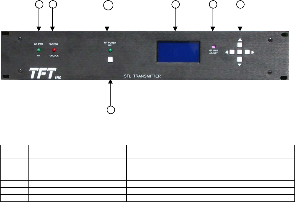
2.3 THE 5290 STL Transmitter FRONT PANEL
The Model 5290 STL Transmitter Front Panel is a collection of input switches and output LEDs, and LCD screen. The
Model 5290 STL Transmitter is illustrated in Figure 2.3-1 and described in Table 2.3-1. Controls and indicators are
located on the Front Panel. Detailed descriptions on the usage and operation of the keys can be found in this Section.
1 2 3 4
7
6 5
Figure 2.3-1. Model 5290 STL Transmitter Front Panel
Table 2.3-1. Model 5290 STL Transmitter Front Panel Controls and Indicators
ITEM TITLE FUNCTION
1 AC POWER LED AC Power On LED Indicator
2 SYSTEM UNLOCK LED Indicates one or more VCOs is unlocked; PA is disabled if “on”.
3 RF POWER LED Indicates radiation of RF power from output
4 LCD Displays transmitter parameters including frequency and power
5 RF POWER ADJUST Adjusts power from 0.5 to 20.0 Watts (R18)
6 NAVIGATION AND ENTRY Scrolls page display and selects items on LCD
7 RF POWER ON/STANDBY SWITCH Turns on for RF power radiation from the unit.
2-1
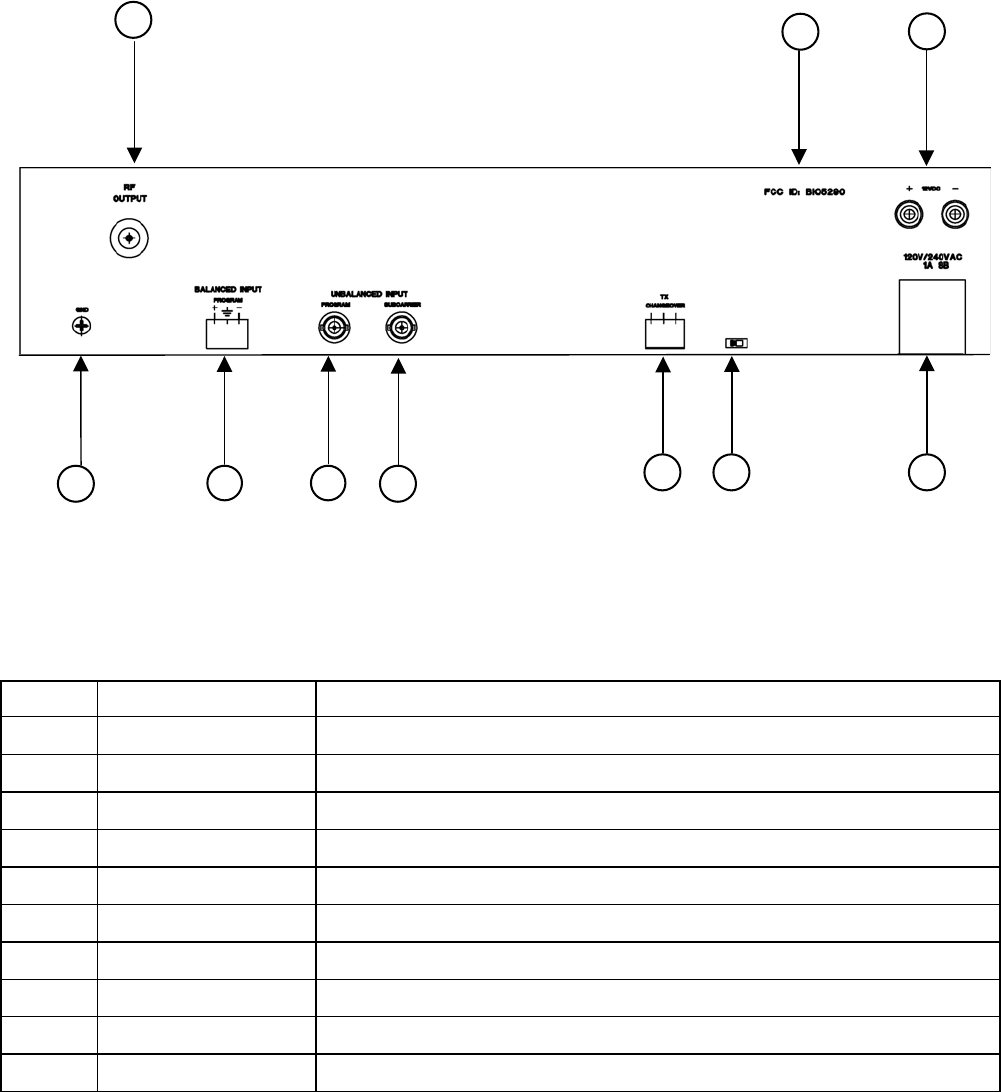
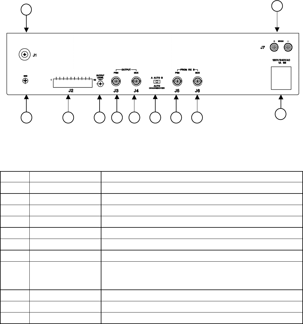
2.4 THE Model 5290 STL TRANSMITTER REAR PANEL
The Model 5290 STL Transmitter Rear Panel has Input/Output connectors for related or optional equipment. Figure 2.4-
1 shows the Rear Panel Configuration.
1 3
2
Figure 2.4-1. Model 5290 STL Transmitter Rear Panel Connectors
5 4 7 10 98
6
Table 2.4-1. Model 5290 STL Transmitter Rear Panel Connectors
ITEM TITLE FUNCTION
1 RF Type N female connector, 50 Ohms
2 FCC ID FCC Type Certification ID
3 12 Vdc Input (optional) Terminals for optional ± 12 Vdc input
4 GND Ground screw connection
5 AUDIO INPUT Screw terminal connection, balanced audio input, 600 Ω
6 PROGRAM Composite program input, unbalanced, BNC 2 Vp-p
7 SUBCARRIER Subcarrier (MUX) input, unbalanced, BNC
8 TX CHANGEOVER Connector for transmitter changeover (TFT Model 7770)
9 AUTO/MAN Switch to set mode of operation with or without transmitter changeover
10 AC INPUT IEC Input connector/fuse assembly
2-2
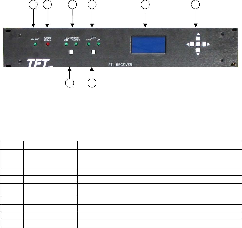
2.5 THE 5291 STL RECEIVER FRONT PANEL
The Model 5291 STL Receiver Front Panel is a collection of input switches and output LEDs, and LCD screen. The
Model 5291 STL Receiver Front Panel is illustrated in Figure 2.5-1 and described in Table 2.5-1.
Controls and indicators are located on the Front Panel. Detailed descriptions on the usage and operation of the keys can
be found in this Section.
1 2 3 4 5
87
6
Figure 2.5-1 Model 5291 STL Receiver Front Panel
Table 2.5-1 Model 5291 STL Receiver Front Panel Indicators and Controls
ITEM TITLE FUNCTION
1 ON LINE “On” indicates receiver is providing output. “Off” indicates that the stand-by
receiver looped through the auto-switchover is providing output or that the
receiver is turned off by remote control.
2 SYSTEM STATUS “On” indicates that VCOs are locked
3 BANDWIDTH “Wide” indicates 500 kHz operation; “Narrow” indicates “300 kHz operation.
4 GAIN “High” indicates that RF input is selected for best sensitivity; “Low” indicates
that gain of 1st RF amplifier is reduced to prevent overload.
5 LCD Multi-page display of receiver operating characteristics and parameters
6 Navigation Keys Used to scroll LCD pages and enter parameters
7 BANDWIDTH Select Toggles between “Wide” and “Narrow” bandwidth operation
8 GAIN Select Toggles gain of 1st RF amplifier between “High” and “Low”
2-3
2.6 THE STL RECEIVER REAR PANEL
The Model 5200 Series STL Receivers Rear Panels have audio and connectors for related or optional equipment. Figure
2.6-1 shows the rear panel configuration.
2
1
ANT
3 4 5 6 11
87 910
Figure 2.6-1 Model 5291 STL Receiver Rear Panel Connectors
Table 2.6-1 Model 5291 STL Receiver Rear Panel Connectors
ITEM TITLE FUNCTION
1 RF INPUT Type N RF input connector, 50 Ohms
2 DC input (optional) Optional ± 12 Vdc input power terminals
3 GND Grounding terminal
4 J2 Terminal connections for mono balanced output and remote controls
5 OUTPUT LEVEL ADJ Adjustment for Program Output level
6 PGM OUTPUT, J3 Program output connector, BNC, unbalanced 3 Vp-p
7 MUX OUTPUT, J4 MUX output connector, BNC, unbalanced
8 AUTO CHANGEOVER Switch to select Auto Changeover operation with another receiver or to
manually select this receiver “A” or another receiver “B” to supply signals to
the OUTPUT connectors
9 RX B PGM, J5 Input from stand-by receiver “B”, program, BNC, unbalanced
10 RX B MUX, J6 Input from stand-by receiver “B”, MUX, BNC, unbalanced
11 AC Input IEC AC power input connector assembly
2-4

2.7 RELATED EQUIPMENT
The Series 5200 STL Transmitters and Receivers can accommodate various components to comprise a complete Studio
to Transmitter Link. Some of this equipment is described in the following paragraphs.
2.7.1 MODEL 7770 AUTOMATIC TRANSMITTER CHANGEOVER UNIT
The Model 7770 Automatic Transmitter Changeover Unit is a switching device that can switch between two transmitters
and furnish a single output for connection to an antenna. There is a separate data sheet available for this product.
2.8 PRE-INSTALLATION INFORMATION
Before installing your STL Transmitter and Receiver, you should be familiar with the requirements of Part 74 of the FCC
rules, as amended. An adequate path survey and analysis is helpful to evaluate the environment and application of the
Digital STL system. Theoretical results obtain from such a path survey and analysis should be compared to actual
installed data in order to establish a benchmark for the system and to document its performance.
Assistance may be obtained from TFT Customer Service.
1953 Concourse Drive
San Jose, California 95131-1708 USA
Tel: (+1) 408 943-9323 Fax: (+1) 408943-9218
Email: techsupport@TFTInc.com
2-5
3-1
SECTION III
PRE-INSTALLATION CHECKOUT
3.1 INTRODUCTION
This section describes a functional bench test to be performed before installing and testing the 5200 Series STL
Transmitter and Receiver according to the procedures given in Section V. By completing the pre-installation checkout,
the user can be certain that the equipment is operating properly.
CAUTION
Do not connect the transmitter
antenna output directly to the
receiver antenna input. Doing so
will damage the receiver input
circuitry.
3.2 PRIMARY POWER APPLICATION
Before power is applied to the 5200 Series STL Transmitter, insure that an adequate load is connected to the RF Output
Connector.
For back-to-back testing, place the transmitter and receiver next to each other. Terminate the transmitter output in a 50
Ohm load of 50 watts or larger rating.
To insure that the transmitter and receiver function as a system, we recommend the following checkout procedure before
final installation of the system.
a. Place the front panel RF POWER ON/STANDBY switch to the STANDBY position.
b. Connect the AC power connectors to the correct line voltage.
c. The units are now ready for test.
4-1
SECTION IV
OPERATING
THE 5200 SERIES ANALOG STL TRANSMITTERS and RECEIVERS
4.1 INTRODUCTION
The 5200 Series of Transmitters and Receivers are conventional composite and mono systems designed to meet
today’s stringent broadcasting requirements. Each transmitter or receiver is fully compatible with other TFT
systems of comparable configuration. The 5200 series of transmitters is designed to fulfill requirements for
composite stereo, composite stereo with MUX, and mono applications. The 5200 series of receivers is available
for composite/mono, composite, and mono only configurations. Frequencies from 140 MHz to 2 GHz will be
available.
4.2 OVERVIEW OF OPERATION
These instructions assume that the units have been configured by the factory and that the Pre-Installation
Checkout has been completed in accordance with the instructions in Section III of this User’s Guide.
4.3 SETTING TRANSMITTER PARAMETERS
See Section II for details of the transmitter front panel and rear panel connections.
Make sure that RF power is turned “off” and that the transmitter is connected to a proper load or antenna.
Pressing the center (ENTER) button to the right of the display will advance the LCD through various pages for
setup.
The default page should have an indication for “FRQ”. Increment the frequency desired for operation with the
“UP” and “DOWN” arrow keys until the desired frequency is displayed. Once the desired frequency is displayed,
press the center (ENTER) button to “load” the desired frequency into the unit.
No further adjustments are required to change frequency. No tuning adjustments are required to change frequency
within the range of frequencies at which the unit operates. It will tune the entire band automatically.
The screw adjustment to the right of the LCD will increment the output power to the desired level between 0.5
Watt and 20 Watts.
The unit is now ready for operation. The RF power “On” switch may be pressed.
4.4 OBSERVING TRANSMITTER OPERATION
The center (ENTER) button to the right of the display to advance through display pages to observe various
operating parameters, including frequency, power output, reflected power, VCO status, etc.
4.5 SETTING RECEIVER PARAMETERS
The receiver operating frequency is set in a fashion similar to that of the transmitter (See Section 4.3 above.).
Pressing the center (ENTER) button to the right of the display will advance the LCD through various pages for
setup.
The default page should have an indication for “FRQ”. Increment the frequency desired for operation with the
“UP” and “DOWN” arrow keys until the desired frequency is displayed. Once the desired frequency is displayed,
press the center (ENTER) button to “load” the desired frequency into the unit.
No further adjustments are required to change frequency. No tuning adjustments are required to change frequency
within the range of frequencies at which the unit operates. It will tune the entire band automatically.
4-2
After the unit is installed, all operating parameters should be recorded in order to establish a baseline for future
maintenance and operation. RSSI (Received Signal Strength Indication) should be noted, along with all VCO and
voltage readings. This will assist trouble shooting in the future by having comparison readings.
5-1
SECTION V
INSTALLATION
5.1 INTRODUCTION
This section describes the installation of the Model 5200 Analog STL Transmitter and Receiver Series and their related
options and equipment after they have been unpacked and tested according to methods described in Section IV.
Electrical ground for the Model 5200 Transmitters and Receivers is established through the AC power cord.
Additionally, there is a grounding stud on the rear of each unit. If a more substantial technical ground is available, it may
be connected to the chassis box directly at the grounding screw, using a short piece of braid. Proper grounding, good
engineering practice, and safety depend on the knowledge and care of the installing engineer.
All units are designed to mount in a 19” rack or cabinet using (4) 12-24 pan head machine screws.
Mounting requirements: Size: 3.5”H x 19”W x 12”D (8.9 cm x 47.5 cm x 30.5 cm) Maximum. Weight:
Approximately 20 pounds (9 kg.)
Power requirements: Input power: 117/240 VAC @ 50/60 Hz, 100 Watts maximum, 3 Prong Power Cord - UL
style SVT
Environmental requirements: 0°C to 50°C (32°F to 122°F).
General Hazards:
a. Elevated Operating Ambient Temperature - If installed in a closed or multi-unit rack assembly, the operating
ambient temperature of the rack environment may be greater than room ambient. Therefore, consideration
should be given to installing the equipment in an environment compatible with the maximum rated ambient
temperature.
b. Reduced Air Flow - Installation of the equipment in a rack should be such that the amount of airflow required
for safe operation of the equipment is not compromised.
c. Mechanical Loading - Mounting of the equipment in a rack should be such that a hazardous condition is not
achieved due to uneven mechanical loading.
d. Circuit Overloading - Consideration should be given to the connection of the equipment to the supply circuit
and the effect that overloading of the circuit might have on over-current protection and supply wiring.
e. Reliable Earthing - Reliable earthing of rack-mounted equipment should be maintained. Particular attention
should be given to supply connections other than direct connections to the branch circuit (e.g., power strip use).
SECTION VI
THEORY OF OPERATION
6.1 GENERAL
This section describes the theory of operation for the Model 5200 Series STL Transmitter and Receivers.
The Model 5200 STL Transmitter accepts either balanced or unbalanced composite or monaural audio on
the rear panel. The composite input level should be 3Vp-p for ± 50 kHz deviation. The program input is
adjusted by R22 on the Main Board. Similarly, there is an unbalanced input for a MUX channel, the level
of which should be 1.2Vp-p for ± 12 kHz deviation. The MUX deviation is adjusted by R29 on the Main
Board.
J10 sets the transmitter for “Flat” composite or monaural operation. J11 sets the transmitter pre-emphasis to
75 µsec; J12 sets the pre-emphasis to 50 µsec. Only one of these three jumpers should be made at any
time.
If the optional SCA generator is utilized, then J19 should be connected between pins 2 and 3; if an external
SCA generator is utilized, the J19 should be connected between pins 1 and 2.
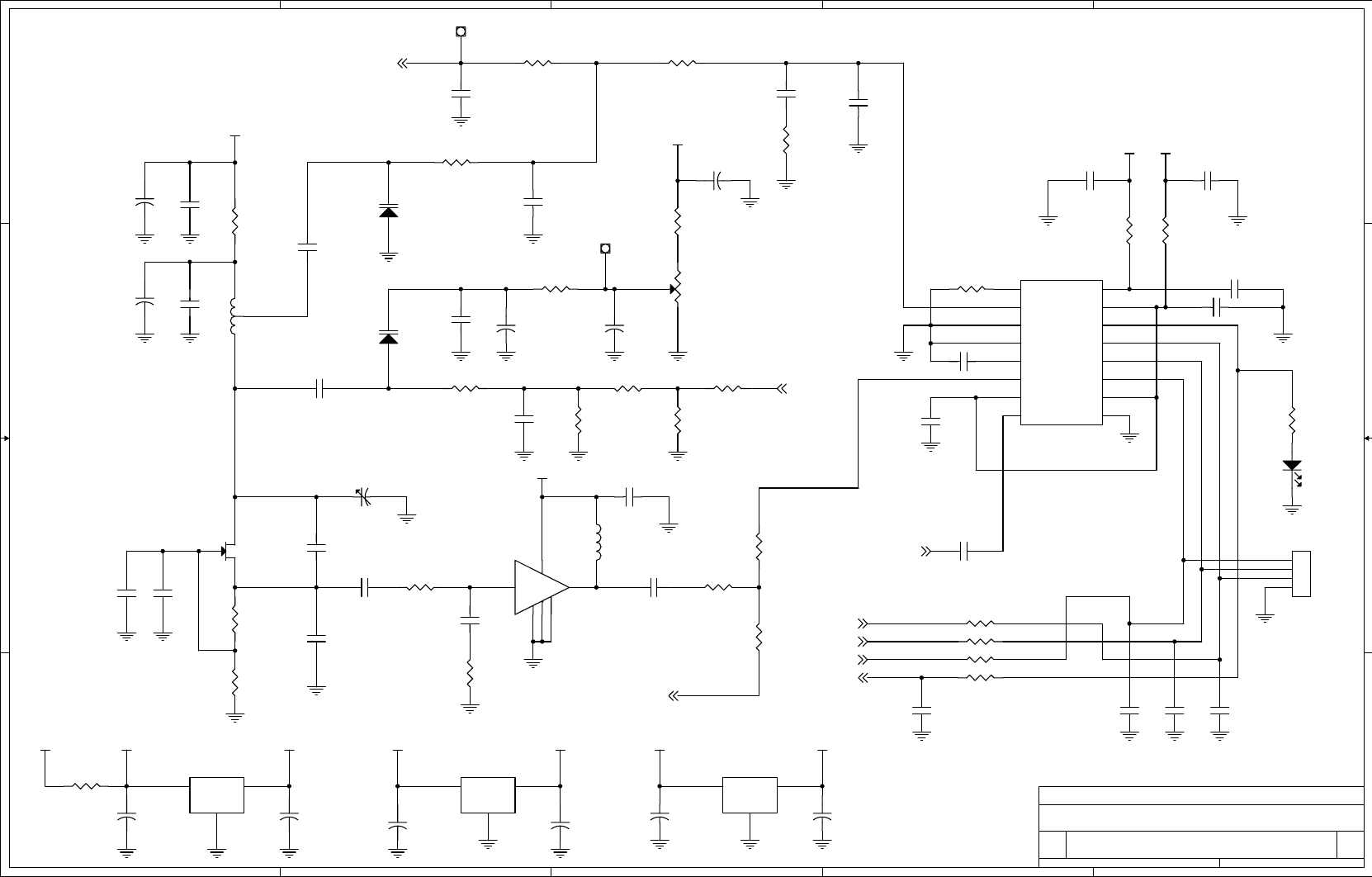
The summed output of the program and SCA networks is routed to a 70 MHz VCO Modulator, which
consists of U14 and U13. Linearity of the modulation is adjusted by R64.
The 70 MHz modulated VCO output (-18 dBm) is mixed in U27 with a local oscillator (+3 dBm), which
operates 70 MHz below the output frequency. This on-frequency, modulated signal (-24 dBm) is filtered
by FL2, then amplified by U28, which adds approximately 30 dB of gain. The output of U28 (+3 dBm) is
again filtered then amplified by U29, a 15 dB gain amplifier, for a final output from the main board of
approximately +15 dBm.
The local oscillator consists of a dual Phase-Lock-Loop, which consists of a TCXO that operates at 20
MHz and U20 (VCO1), VCO2 and U21. The frequency is referenced to the 20 MHz TCXO and actually
set by U19 and U24, which are controlled by logic programmed by U1.
The modulated, on-frequency RF output of the main board is routed to the input of the power amplifier,
where the signal is furthered amplified and filtered by U1 and strip-line filters on the Power Amplifier
Board.
U10, U11, U6A, U8A on the Main Board control lock-out and remote control functions. Metering samples
for PGM, MUX, FWD PWR, REV PWR, VCO1 bias, VCO2 bias, and VCO3 bias are furnished to U1 and
subsequently scaled and displayed by the front panel LCD.
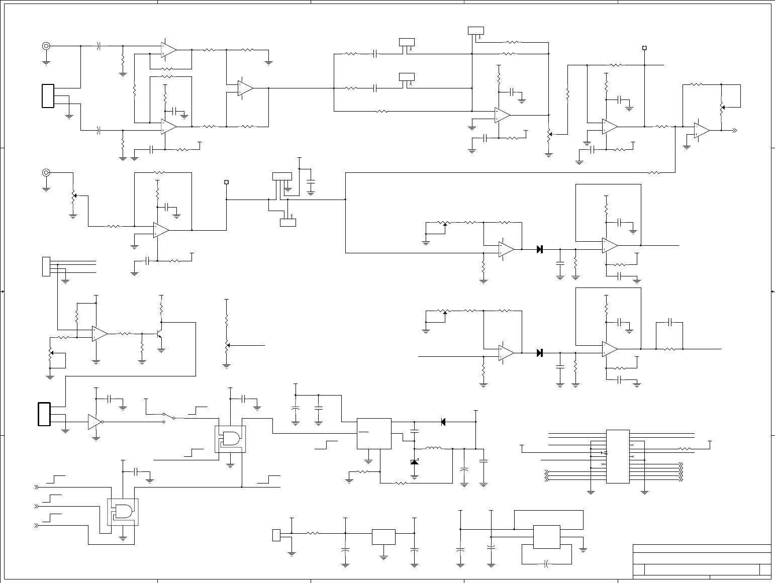
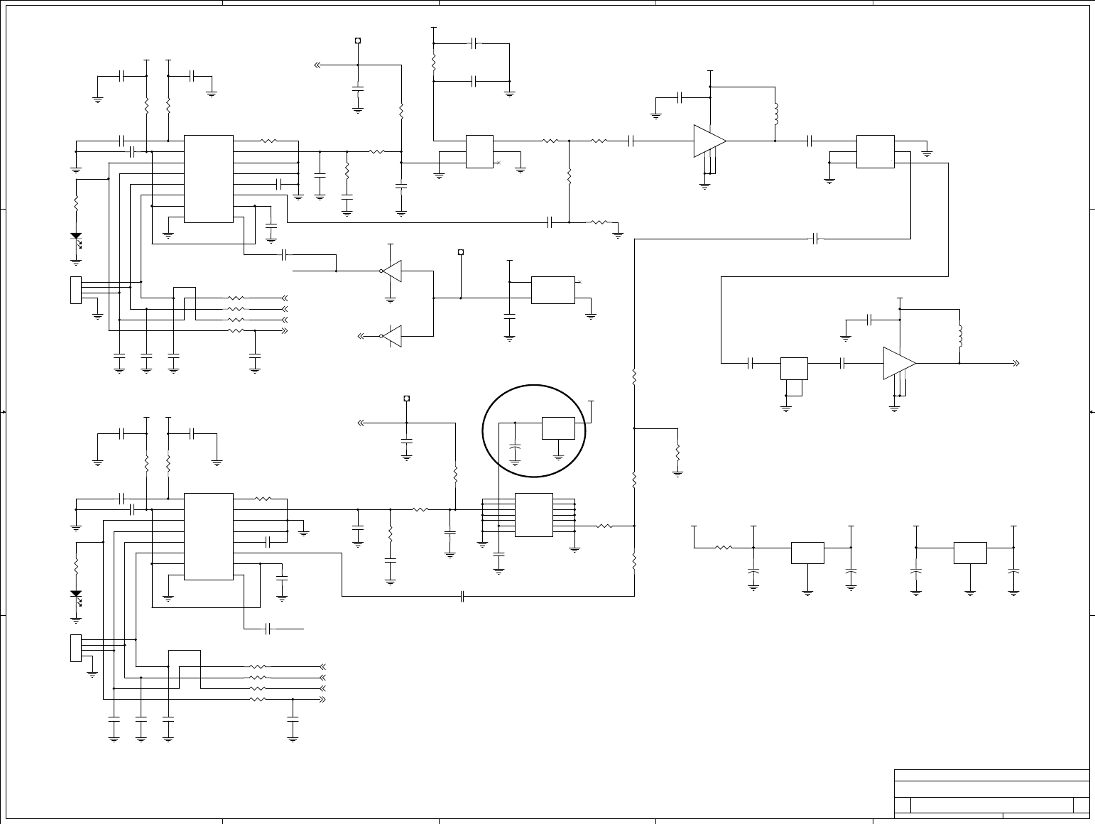
6.2 MODEL 5200 STL TRANSMITTER BASIC DIAGRAM DESCRIPTION
The 5290 Transmitter consists of a Main Board, a Display Board, a Power Amplifier, and a power supply.
The Main Board contains input processing and metering, the local oscillator, mixer, and RF output circuits.
The Display Board receives display information from the Main Board for display on the front panel LCD.
The Power Amplifier amplifies the modulated, on-frequency RF output from the Main Board to the proper
RF output level on the rear panel.
6.3 MODEL 5291 STL RECEIVER BASIC DIAGRAM DESCRIPTION
(To be supplied)
6-1
SECTION VII
MAINTENANCE AND REPAIR
7.1 INTRODUCTION
The 5200 Series STL Transmitter and Receiver have no moving parts or components that require routine
replacement. They require only minor audio adjustment.
7.2 TOOL AND TEST EQUIPMENT REQUIREMENTS
The following tools and equipment are required for analog STL system maintenance:
• Hand Tools • RF Spectrum Analyzer, 10 GHz
• Digital Voltmeter • RF Signal Generator, 2 GHz
• Oscilloscope • RF Load, 50 Ω, 25 Watts
• Audio generator • Stereo generator/coder
• Audio analyzer/noise/distortion • Stereo demodulator/modulation monitor
7.3 ROUTINE MAINTENANCE
The Series 5200 STL Transmitter and Receiver should require no routine maintenance. As equipment and
systems external to the Transmitter and Receiver change, minor audio level adjustments may be necessary.
7.3.1 CALIBRATION
The Series 5200 STL Transmitter and Receiver do not require routine calibration.
7.4 DIAGNOSTICS AND REPAIR
Before attempting repair, the tools and test equipment listed in Section 7.2 should be on hand. Only limited
diagnostics and repairs can be accomplished without a complete set of equipment listed. The most practical repair
philosophy is by the factory. It is recommended that a stand-by unit be on hand, together with an alternative plan
for operation while factory repairs are being made. Spares kits are available from the factory. Rental and
emergency units are available from the factory during repairs.
Some general (and very important) observations on repair:
1. The STL equipment uses static sensitive components. ESD (Electrostatic Discharge) precautions must therefore
be observed during repairs. This is extremely important.
2. The Theory of Operation Section (Section VI) is helpful in understanding how the equipment functions and
will help you with diagnostics, as it covers the jobs performed by each major component and subsystem.
7.5 TFT CUSTOMER SERVICE DEPARTMENT
TFT emergency service is available 24 hours a day. Please call us if you need assistance with any TFT products.
TFT, Inc.
1953 Concourse Drive
San Jose, California 95131-1708 USA
Telephone: (+1) 408 943-9323, Fax: (+1) 408 943-9218
Email: techsupport@TFTInc.com
7-1
SECTION VIII
ENGINEERING DRAWINGS
Model 5290 Transmitter
Title Dwg. No. Rev
Main Board: Meter and Interface 6601-4128 (1 of 4) 1
Main Board: 70 MHz VCO Modulator 6601-4128 (2 of 4) 1
Main Board: Up Converter, Filter Amp 6601-4128 (3 of 4) 1
Main Board: Dual PLL Up Converter, LO 6601-4128 (4 of 4) 1
Power Amplifier 6601-4129 1
Display Board (for 5290 & 5291) 6601-4132 1
8-1
A
A
B
B
C
C
D
D
E
E
4 4
3 3
2 2
1 1
PGM
PGM+
PGM-
3Vp-p for
+/- 50KHz DEV.
1.2Vp-p for
+/- 12.5KHz DEV.
4V for 100% DEV. Deviation
ADJ
Locked
PA ON
PA ON
20mA
MUX
B
SW
LED
75uS
50uS
Rear Panel
Rear Panel
Rear Panel
Jumper
ADC
ADC
ADC
ADC
ADC
ADC
ADC
Locked
Locked
Locked
SCA
Generator
Rear Panel Rear Panel
POT
POT
From PA
Module
1V for 100% DEV.
Composit Mono
Local
Remote
PA ON
From Switching Power supply
Transmitter
D
Automatic
Changeopver
+4V for 100% Deviation
TFT INC.
METER and INTERFACE
6601-4128
1
Model 5290 MAIN BOARD
C
14Wednesday, April 06, 2005
Title
Size Document Number Rev
Date: Sheet of
MUX_METER
PGM_METER
PA-ON
SYSTEMLOCKEDPA-ON
REV_PWR
FWD_PWR
PGM
PGM_METER
PWR_ADJ
SYSTEMLOCKED
FWD_PWR
REV_PWR
PGM
MUX_METER
PWR_ADJ
PWR_ADJ
MODULATION
LE_3
LE_2
LE_1
CLK
DATA
LD_VCO3
LD_VCO2
LD_VCO1
BIAS_VCO1
BIAS_VCO2
BIAS_VCO3
+12VC
+5VC
+12VC
+5VC
+12VC
+5VC
+5VC
+5VC
-5V
+5VC
+5VC
-5V
+5VC
+5VC
-5V
-5V
+5VC
-5V
-5V
+5VC -5V
+5VS
+12VC
+5VC+12VC
+5VS
+12V
+5VS
+12V
R26
10
C10
1uF
R2
10K
R8
10K
R9
10K
R13
10K
R132
100
C22
0.1uF
R10
10
J5
CON2
1
2
C4
1uF
+
C21
22uF
R21
TBD
R12
TBD
C138
0.1uF
R19
10K
-
U2A
LF353D
3
2
1
48
R20
4.7K
R6
10K
R50
1M
C18
0.22uF
R28
TBD
R29
2K
-
U1A
LF353D
3
2
1
4 8
-
U1B
LF353D
5
6
7
4 8
U12
LTC1983ES6
1
2
3 4
6
5
VCC
VOUT
C+ C-
/SHDN
GND
CR3
CMDSH-3
+
C1
47uF
+
C7
47uF
R4
100
R18
49.9K
-
U2B
LF353D
5
6
7
4 8
C2
1.5nF
R5
49.9K
R43
1K R44
10K
-
U7A
LF353D
3
2
1
4 8
R31
10
C13
1uF
R14
100
-
U7B
LF353D
5
6
7
4 8
R17
10K
R34
22K
R33
1K
-
U5B
LF353D
5
6
7
4 8
R38
10K
CR1
HSMS2800
1 3
R32
10K
-
U5A
LF353D
3
2
1
4 8
R37
1M
C15
0.22uF
J19
CON4
1
2
3
4
-
U3B
LF353D
5
6
7
4 8
U32
L78L05ABU
3
2
1
IN
G
OUT
R133
0
J11
CON3
1
2
3
J3
BNC
1
2
TP2
1
TP1
1
R41
10
C17
1uF
R7
TBD
R52
10K
J10
CON3
1
2
3
VCCGND
U10
NC7SZ11P6X
1
2
3 4
5
6
R42
10K
J4
1
2
3
1
2
3
C11
1uF
R49
2K
J1
1
2
3
1
2
3
-
U6A
LF353D
3
2
1
4 8
R47
220
R24
10K
C16
1uF
R39
10
R45
10K
C3
1nF
R3
4.7K
J16
CON3
1
2
3
-
U3A
LF353D
3
2
1
4 8
C25
0.01uF
R22
10K
R25
10
R1
TBD
R15
TBD
J2
BNC
1
2
C9
1uF
C139
0.1uF
R30
10
R16
10
C12
1uF
J9
CON3
1
2
3
S1
SW SPDT
R130
Not use
C6
1uF
+
C24
10uF
R36
10
J8
CON4
1
2
3
4
CR2
HSMS2800
1 3
Q1
MMBT2222
C14
1uF
R46
10K
R40
1K
+
C141
10uF
+
C142
10uF
+
C26
10uF
+
C27
10uF
J6
CON26A
1
3
5
7
9
11
13
15
17
19
21
23
25
2
4
6
8
10
12
14
16
18
20
22
24
26
+
C28
10uF
R55
43K
R54
12K
R131
2K
13
2
U9
LT1616ES6
1
2
3
4
5
6
BOOST
GND
FB
SHDN
Vin
SW
R23
10
C8
1uF
R53
10
C20
1uF
R51
1M
VCCGND
U11
NC7SZ11P6X
1
2
3 4
5
6
C140
0.1uF
R27
10K
R35
10K
-
U4A
LF353D
3
2
1
4 8
CR4
MBR0530
2 1
R11
10
C19
0.22uF
C5
1uF
L1
47uH
U8A
NC7WP14
1 6
52
C23
0.022uF
R48
10K
A
A
B
B
C
C
D
D
E
E
4 4
3 3
2 2
1 1
VT
MOD
VCO
OUTPUT
30mA
+4.5V
Linearity Adj
70MHz VCO Modulator
TFT INC.
6601-4128
1
Model 5290 MAIN BOARD
B
24Wednesday, April 06, 2005
Title
Size Document Number Rev
Date: Sheet of
LE_3
DATA
CLK
REF_20MHZ_2
VCO3
LD_VCO3
BIAS_VCO3
MODULATION
+8VB
+12VB +3.3VB +5VB+12VB
+3.3VB
+5VB
+5VB
+12VB +8VB+12V
+8VB
C37
TBD
U14
UPC2710TB
1 4
3
2
5
6
C60
0.1uF
C36
0.01uF
C51
0.01uF
+
C35
47uF
+
C44
10uF
+
C40
47uF
+
C66
10uF
+
C65
10uF
+
C64
10uF
+
C32
10uF
+
C67
10uF
+
C69
10uF
+
C68
10uF
C55
1nF
R61
1K
Q2
MMBFU310LT1
3
1
2
C61
220pF
C62
220pF
C63
220pF
U17
L78L08ABU
3
2
1
IN
G
OUT
CR5
BB639C
1 3
R59
100K
R74
18
R64
1K, 19T
1 3
2
R72
18
R77
18
C50
3~20pF
C59
82pF
C52
47pF
L2
IND_CT
1 3
2
R73
470
R75
220
R81
220
C54
6.8pF
C47
27pF
C38
100pF
L3
2.2uH
U13
ADF4113BRU
1
2
3
4
5
6
7
8 9
10
11
12
13
14
15
16
Rset
CP
CPGND
AGND
RFinB
RFinA
AVDD
REFin DGND
SDVdd
CLK
DATA
LE
MUXOUT
DVdd
VP
C33
0.01uF
C34
0.01uF
R79 2K
C49
0.01uF
R66
5.1K
R63
10
C39 1uF
C46 0.01uF
R62
10
C53
1nF
C42
1uF
+
C45
10uF
U16
L78L05ABU
3
2
1
IN
G
OUT
U15
L78L33ACU
3
2
1
IN
G
OUT
R65
10K
TP4
1
C58
1nF
R80
51
C41
0.01uF
R78 2K
R134
0
R76 2K
J20
CON4
1
2
3
4
C43
0.01uF
R137
470
D1
LED
TP3
1
C29
1nF
R56
100K
R60
150
R69
4.7K
R71
820
C31
TBD
R58
TBD
C30
TBD
R67
2.2K
R68
4.7K
CR6
BB639C
1 3
R57
TBD
R82 22K
R70
1.5K
C48
33pF
C57
1nF
C56
22uF
A
A
B
B
C
C
D
D
E
E
4 4
3 3
2 2
1 1
20MHz TCXO
GAIN=30dB
-27dBm +3dBm
-6dBm +7dBm
+7dBm
-18dBm
-24dBm
870~890MHz
55~65MHz
815~825MHz
50mA
was VCO1
was
U20
TFT INC.
DUAL PLL UP CONVERTOR LO
6601-4128
1
Model 5290 MAIN BOARD
C
34Wednesday, April 06, 2005
Title
Size Document Number Rev
Date: Sheet of
REF_20MHZ_1
REF_20MHZ_1
LE_1
DATA
CLK
LD_VCO1
REF_20MHZ_2
LO
BIAS_VCO1
BIAS_VCO2
LD_VCO2
CLK
DATA
LE_2
+5VA
+5VA
+5VA+3.3VA
+3.3VA
+3.3VA
+5VA
+12VA +3.3VA +5VA+12VA+12V
+3.3VA +5VA
+5VA
R91
1K
U19
ADF4106BRU
1
2
3
4
5
6
7
89
10
11
12
13
14
15
16 Rset
CP
CPGND
AGND
RFinB
RFinA
AVDD
REFinDGND
SDVdd
CLK
DATA
LE
MUXOUT
DVdd
VP R90
0
U24
ADF4113BRU
1
2
3
4
5
6
7
89
10
11
12
13
14
15
16 Rset
CP
CPGND
AGND
RFinB
RFinA
AVDD
REFinDGND
SDVdd
CLK
DATA
LE
MUXOUT
DVdd
VP
C96
0.01uF
C97
0.01uF
R88
18
C104
0.01uF
C110
0.01uF
R111
2K
C99
1uF
R83
18
R100
10
R104
5.1K
C100 1uF
C112
1nF
R101
10
R110
2K
R109
2K
R112
22K
+
C126
47uF
C71
0.01uF
C72
0.01uF
C70
0.01uF
R86
100K
VCO1
VCO MQE001
2
43
1
5
6
G
outVcc
Vt
G
M
C73
1nF
R138
470
R108
18
TP5
1
D2
LED
U18
UPC2708TB
1 4
3
2
5
6
C98
1nF
R135
0
C75
0.01uF
C77
220pF
R102
100K
TP6
1
J21
CON4
1
2
3
4
C115
220pF
C105
1uF
C85
0.01uF
+
C106
10uF
+
C107
10uF
+
C108
10uF
+
C109
10uF
R106
18
R103
18
C87
1nF
R139
470
D3
LED
TP7
1
J22
CON4
1
2
3
4
C91
220pF
C90
220pF
C92
220pF
U25
L78L33ACU
3
2
1
IN
G
OUT
U26
L78L05ABU
3
2
1
IN
G
OUT
U22A
NC7WP14
16
52
C101
0.15uF
C93
0.01uF
C83
0.015uF
C80
Not use
C81
10pF
R96 2K
R94 2K
R95 2K
R87
5.1K
U22B
NC7WP14
34
52
C82
0.01uF
R105
2.7K
R107
300
C102
2.2uF
C84
56pF
U33
Regulator SOT89
3
2
1IN
G
OUT
R93
51
R92
18
C103
0.082uF
L4
0.27uH
FL1
Epcos B7704
1 3
4
2
IN OUT
G
G
C89
0.01uF
C95
220pF
U23
UPC2710TB
1 4
3
2
5
6
C78
220pF
C86
1nF
L5
0.27uH
R97 22K
U21
ADEX-10L
1
4
2
3
5
6GND
GND
IF
RF
GND
LO
R99
TBD
R98
TBD
C88
1uF
C94
220pF
C74
1uF
R89
18
C114
220pF
C113
220pF
C116
0.01uF
VCO2
JTOS-100
5
132
1
3
4
6
7 8
9
10
11
12
14
VT
OUTVCC
GNG
GND
GND
GND
GND GND
GND
GND
GND
GND
GND
R84
10
C76
1uF
C111
1nF
FOX801BE
Y1
14
3 2
VCVDD
OUTPUT GND
C79
1uF
R85
10
A
A
B
B
C
C
D
D
E
E
4 4
3 3
2 2
1 1
940~960MHz
+15dbm
GAIN=30dB
-24dBm
-18dBm
+3dBm
-27dBm +3dBm
GAIN=15dB
0dBm
90mA
70MHz
870~890MHz
29mA MAX.
60mA MAX.
RF OUTPUT
TFT INC.
Up Converter, Filter Amp
6601-4128
1
Model 5290 MAIN BOARD
A
44Thursday, April 07, 2005
Title
Size Document Number Rev
Date: Sheet of
VCO3
LO
+5VD
+5VD
+5VS
U28
UPC2710TB
1 4
3
2
5
6
U29
UPC1678GV
1 5
84
2
3
6
7
C125
220pF
R116
0
FL2
Epcos B7707
1 3
4
2
IN OUT
G
G
C120
220pF
C117
1uF
J7
RF JACK
1
2
C122
220pF
L7
0.27uH
C124
220pF
2 1
L6
0.27uH
R136
0
C121
1nF
R114
TBD
R113
TBD
C118
220pF
R115
TBD
FL3
Epcos B7707
1 3
4
2
IN OUT
G
G
R117
not use
R118
not use
U27
ADEX-10L
1
4
2
3
5
6GND
GND
IF
RF
GND
LO
C123
1uF
C119
220pF
5
5
4
4
3
3
2
2
1
1
D D
C C
B B
A A
RF Output
1mA @5V
940~960MHz
+15dbm
RF INPUT
To Fan
+
-
12V
Jumper Wire
TFT INC.
From Switching
Power Supply
6601-4129 1
Model 5290 Power Amplifier
B
11Wednesday, April 06, 2005
Title
Size Document Number Rev
Date: Sheet of
FWD_PWR_PA
REV_PWR_PA
REV_PWR_PA
FWD_PWR_PA
PWR_ADJ_PA
PWR_ADJ_PA
+12V
CP1
Coupler
1 2
3 4
5 6
C1
47pF 100V
21
J1
Type N JACK
1
2
R4
10K C2
1nF
U1
<>
RA20H8994M
41
2
3
OUTIN
VGG
VDD
C4
1nF
R1
10K
J3
RF JACK
1
2
C9
1nF
CR1
HSMS2800
3 1
R5
56
CR2
HSMS2800
31
C3
1nF
R7
10K
L1
Shield Bead
J4
CON3
1
2
3
L2
Shield Bead
R2
56
R6
56
R3
56
J2
CON4
1
2
3
4
FL1
MicroStrip LPF
1 2
R9
0
R8
Not Use
R10
Not Use
+
C6
10uF
+
C5
10uF
+
C7
10uF
+
C8
10uF
5
5
4
4
3
3
2
2
1
1
D D
C C
B B
A A
FRONT PANEL
FRONT PANEL
FRONT PANEL
ADC
ADC
RF POWER ADJ
LED
FRONT PANEL
FRONT PANEL
SW
POT
POT
ADC
ADC
ADC
ADC
ADC
FRONT PANEL
FRONT PANEL
FRONT PANEL
AC POWER ON
RF POWER ON
RF POWER ON
(BANDWIDTH
WIDE/NARROW)
(BANDWIDTH
NARROW)
(RX GAIN HI/LOW)
For Receiver only
< 100mA< 20mA
LCD
Connector
To LCD
Backlight
System Locked
( RX SYSTEM
STATUS)
(RX ON LINE)
TFT INC.
(BANDWIDTH
WIDE)
FRONT PANEL
FRONT PANEL
(RX GAIN LOW)
WIDE
(RX GAIN HIGH)
RF POWER ON
(RX GAIN HIHG)
SYSTEM UNLOCKED
75mA MAX.
to Pin 14 of U2,U5
to Pin 7 of U2,U5
LEFT UP RIGHT DOWN ENTER
FRONT PANEL (RF GAIN HIGH/LOW)
6601-4132
1
Model 5290 Display Board
C
11Wednesday, April 06, 2005
Title
Size Document Number Rev
Date: Sheet of
BIAS_VCO1
P1.1/TA0
-VREF/-VeREF
Ve_REF+
P1.0/TACLK
LE_3
DATA
CLK
FWD_PWR
LE_3
PWR_ADJ
REV_PWRPGM_METER
CLK
LE_1
DATA
SYSTEMLOCKED
MUX_METER
PA_ON
BIAS_VCO2
BIAS_VCO3
BIAS_VCO1
LE_2
REV_PWR
FWD_PWR
BIAS_VCO3
V_REF+
LE_2
LE_1
SYSTEMLOCKED
PGM_METER
BANDWIDTH_WIDE/NARROW
MUX_METER
BIAS_VCO2
PA_ON
BANDWIDTH_WIDE/NARROW
+3.3V
+5V
+3.3V +5V
+12V
+12V
+12V
+3.3V
+3.3V
+5V
D7
LED(GREEN)
J2
CON30
1
2
3
4
5
6
7
8
9
10
11
12
13
14
15
16
17
18
19
20
21
22
23
24
25
26
27
28
29
30
CS1
RES
A0
WR
RD
D0
D1
D2
D3
D4
D5
D6
D7
Vcc
GND
VOUT
CAP3-
CAP1+
CAP1+
CAP2-
CAP2+
V1
V2
V3
V4
V5
VR
C28
P/S
IRS
C7
12pF
R7
100K
U1
MSP430F135
1
2
3
4
5
6
7
8
9
10
11
12
13
14
15
16
17
18
19
20
21
22
23
24
25
26
27
28
29
30
31
32
33
34
35
36
37
38
39
40
41
42
43
44
45
46
47
48
49
50
51
52
53
54
55
56
57
58
59
60
61
62
63
64
DVcc
P6.3/A3
P6.4/A4
P6.5/A5
P6.6/A6
P6.7/A7
V REF+
XIN
XOUT
VeREF+
V REF-/VeREF-
P1.0/TACLK
P1.1/TA0
P1.2/TA1
P1.3/TA2
P1.4/SMCLK
P1.5/TA0
P1.6/TA1
P1.7/TA2
P2.0/ALK
P2.1/TAINCLK
P2.2/CAOUT/TA0
P2.3/CA0/TA1
P2.4/CA1/TA2
P2.5/Rosc
P2.6/ADC12CLK
P2.7/TA0
P3.0/STE0
P3.1/SIMO0
P3.2/SOMI0
P3.3/UCLK0
P3.4/UTXD0
P3.5/URXD0
P3.6
P3.7
P4.0/TB0
P4.1/TB1
P4.2/TB2
P4.3
P4.4
P4.5
P4.6
P4.7/TBCLK
P5.0
P5.1
P5.2
P5.3
P5.4/MCLK
P5.5/SMCLK
P5.6/ACLK
P5.7/TBOUTH
XT2OUT
XT2IN
TDO/TDI
TDI/TCLK
TMS
TCK
RES/NMI
P6.0/A0
P6.1/A1
P6.2/A2
AVss
DVss
AVcc
R3
47K
R2
10K
D2
LED(GREEN)
TP14
1
TP15
1
C3
4.7uF
2 1
R6
2.2K
TP16
1
TP17
1
TP18
1
R18
100
TP19
1
TP20
1
TP21
1
TP22
1
TP1
1
TP2
1
TP3
1
TP4
1
TP5
1
TP6
1
TP7
1
R1
10K
TP8
1
TP9
1
TP10
1
TP11
1
TP12
1
TP13
1
TP39 1
TP41 1
R20
2.2K
R19
2.2K
D5
LED(GREEN)
SW1
SPST
12
C16
1uF
2 1
J1
Header 14pins
1
3
5
7
9
11
2
4
6
8
10
12
13 14
1
3
5
7
9
11
2
4
6
8
10
12
13 14
D4
LED(GREEN)
R15
2.2K
SW7
SPST
12
D3
LED(GREEN)
R14
2.2K
U2D
7404
98
C15
0.047uF
2 1
R16
220K
R13
4.7K
U2B
7404
34
R21
2.2K
C8
1uF
2 1
TP43 1
U3
L78L33ACU
3
2
1
IN
G
OUT
TP28
1
TP30
1
TP31
1
TP32
1
TP33
1
TP34
1
TP35
1
TP36
1
TP37
1
TP38
1
TP40
1
TP42
1
TP44
1
TP45
1
TP46
1
C18
1uF
2 1
C17
1uF
2 1
C9
1uF
2 1
TP24 1C12
1uF
2 1
C11
1uF
2 1
C10
1uF
2 1
TP26 1
TP27 1
TP29 1
TP48
1
TP49
1
R8
100K
TP47
1
TP23
1
TP25
1
U4
L78L05ABU
3
2
1
IN
G
OUT
C20
1uF
2 1
U2C
7404
56
C19
1uF
2 1
U2F
7404
1312
U2E
7404
1110
U5A
7404
12
Y1
32.768KHz
U2A
7404
12
D1
LED(GREEN)
R5
2.2K
C6
4.7uF
21
J4
CON2
1
2
C5
4.7uF
21
R12
220K
C14
0.047uF
2 1
R17
5K
1 3
2
R4
4.7K
C4
4.7uF 21
SW3
SPST
1 2
C13
12pF
C1
10uF
J3
CON26A
1
3
5
7
9
11
13
15
17
19
21
23
25
2
4
6
8
10
12
14
16
18
20
22
24
26
SW4
SPST
1 2
SW2
SPST
1 2
SW6
SPST
1 2
SW5
SPST
1 2
D6
LED( RED)
C2
100nF
R9
100K
R10
100K
R11
100K