THALES DIS AlS Deutschland ELS61-USA LTE/WCDMA Module ELS61-USA User Manual els61 usa hid
Gemalto M2M GmbH LTE/WCDMA Module ELS61-USA els61 usa hid
UserManual.wiki
>
THALES DIS AlS Deutschland
>
ELS61 USA User Manual
user manual_els61-usa_hd_v01040a
Navigation menu
Upload a User Manual
Namespaces
Wiki Guide
HTML
PDF
Info
Views
User Manual
Discussion / Help
Navigation
![Cinterion® ELS61-USA Hardware Interface Description1.1 Key Features at a Glance14els61-usa_hid_v01.040a 2017-08-31Confidential / PreliminaryPage 10 of 113SMS Point-to-point MT and MOCell broadcastText and PDU modeStorage: SIM card plus SMS locations in mobile equipmentSoftwareAT commands Hayes 3GPP TS 27.007, TS 27.005, Gemalto M2MAT commands for RIL compatibility Java™ Open Platform Java™ Open Platform with • Java™ profile IMP-NG & CLDC 1.1 HI• Secure data transmission via HTTPS/SSL1• Multi-threading programming and multi-application executionMajor benefits: seamless integration into Java applications, ease of pro-gramming, no need for application microcontroller, extremely cost-efficient hardware and software design – ideal platform for industrial applications.The memory space available for Java programs is 30MB in the flash file system and 18MB RAM. Application code and data share the space in the flash file system and in RAM.Microsoft™ compatibility RIL for Pocket PC and Smartphone SIM Application Toolkit SAT letter classes b, c, e; with BIPAudio Support for Voice over LTE (VoLTE), i.e. Voice Service via IMS (IP-based Multimedia Subsystem) with CSFBFirmware update Generic update from host application over ASC0 or USB modem. InterfacesModule interface Surface mount device with solderable connection pads (SMT application interface). Land grid array (LGA) technology ensures high solder joint reli-ability and allows the use of an optional module mounting socket.For more information on how to integrate SMT modules see also [3]. This application note comprises chapters on module mounting and application layout issues as well as on additional SMT application development equip-ment.USB USB 2.0 High Speed (480Mbit/s) device interface, Full Speed (12Mbit/s)compliant2 serial interfaces ASC0 (shared with GPIO lines):• 8-wire modem interface with status and control lines, unbalanced, asyn-chronous• Adjustable baud rates: 1,200bps to 921,600bps• Autobauding: 1,200bps to 230,400bps• Supports RTS0/CTS0 hardware flow control.ASC1 (shared with GPIO lines):• 4-wire, unbalanced asynchronous interface• Adjustable baud rates: 1,200bps to 921,60bps• Autobauding: 1,200bps to 230,400bps• Supports RTS1/CTS1 hardware flow controlFeature Implementation](https://usermanual.wiki/THALES-DIS-AlS-Deutschland/ELS61-USA/User-Guide-3601224-Page-10.png)
![Cinterion® ELS61-USA Hardware Interface Description2.1 Application Interface59els61-usa_hid_v01.040a 2017-08-31Confidential / PreliminaryPage 25 of 1132.1.3.1 Reducing Power ConsumptionWhile a USB connection is active, the module will never switch into SLEEP mode. Only if theUSB interface is in Suspended state or Detached (i.e., VUSB_IN = 0) is the module able toswitch into SLEEP mode thereby saving power. There are two possibilities to enable power re-duction mechanisms:• Recommended implementation of USB Suspend/Resume/Remote Wakeup:The USB host should be able to bring its USB interface into the Suspended state asdescribed in the “Universal Serial Bus Specification Revision 2.0“1. For this functionality towork, the VUSB_IN line should always be kept enabled. On incoming calls and other eventsELS61-USA will then generate a Remote Wakeup request to resume the USB host control-ler.See also [5] (USB Specification Revision 2.0, Section 10.2.7, p.282):"If USB System wishes to place the bus in the Suspended state, it commands the Host Con-troller to stop all bus traffic, including SOFs. This causes all USB devices to enter the Sus-pended state. In this state, the USB System may enable the Host Controller to respond tobus wakeup events. This allows the Host Controller to respond to bus wakeup signaling torestart the host system."• Implementation for legacy USB applications not supporting USB Suspend/Resume:As an alternative to the regular USB suspend and resume mechanism it is possible toemploy the RING0 line to wake up the host application in case of incoming calls or eventssignalized by URCs while the USB interface is in Detached state (i.e., VUSB_IN = 0). Everywakeup event will force a new USB enumeration. Therefore, the external application has tocarefully consider the enumeration timings to avoid loosing any signalled events. For detailson this host wakeup functionality see Section 2.1.14.3. To prevent existing data call con-nections from being disconnected while the USB interface is in detached state (i.e., VUS-B_IN=0) it is possible to call AT&D0, thus ignoring the status of the DTR line (see also [1]).1. The specification is ready for download on http://www.usb.org/developers/docs/](https://usermanual.wiki/THALES-DIS-AlS-Deutschland/ELS61-USA/User-Guide-3601224-Page-25.png)
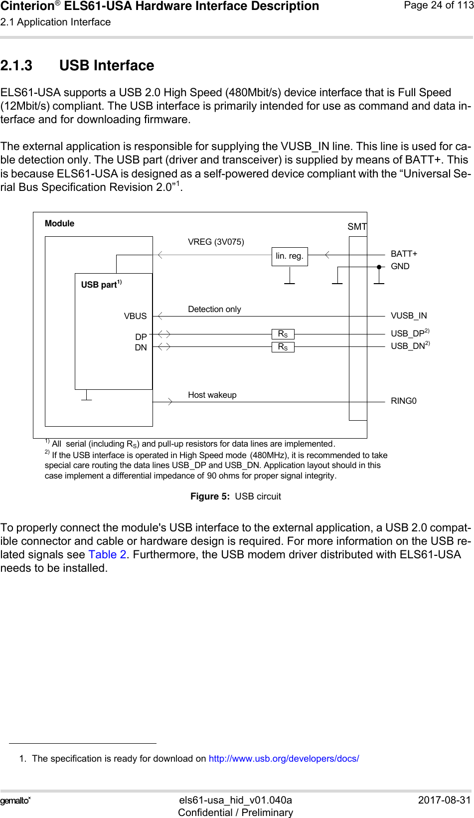
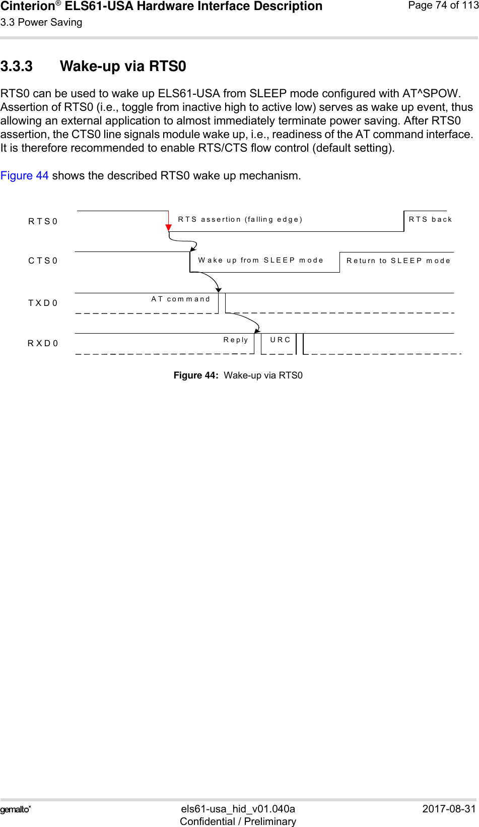
![Cinterion® ELS61-USA Hardware Interface Description2.1 Application Interface59els61-usa_hid_v01.040a 2017-08-31Confidential / PreliminaryPage 26 of 1132.1.4 Serial Interface ASC0ELS61-USA offers an 8-wire unbalanced, asynchronous modem interface ASC0 conforming to ITU-T V.24 protocol DCE signalling. The electrical characteristics do not comply with ITU-T V.28. The significant levels are 0V (for low data bit or active state) and 1.8V (for high data bit or inactive state). For electrical characteristics please refer to Table 2. For an illustration of the interface line’s startup behavior see Figure 7.ELS61-USA is designed for use as a DCE. Based on the conventions for DCE-DTE connec-tions it communicates with the customer application (DTE) using the following signals:• Port TXD @ application sends data to the module’s TXD0 signal line• Port RXD @ application receives data from the module’s RXD0 signal lineFigure 6: Serial interface ASC0Features:• Includes the data lines TXD0 and RXD0, the status lines RTS0 and CTS0 and, in addition,the modem control lines DTR0, DSR0, DCD0 and RING0.• The RING0 signal serves to indicate incoming calls and other types of URCs (UnsolicitedResult Code). It can also be used to send pulses to the host application, for example towake up the application from power saving state. • Configured for 8 data bits, no parity and 1 stop bit. • ASC0 can be operated at fixed bit rates from 1,200bps up to 921,600bps.• Autobauding supports bit rates from 1,200bps up to 230,400bps.• Supports RTS0/CTS0 hardware flow control. The hardware hand shake line RTS0 has aninternal pull down resistor causing a low level signal, if the line is not used and open.Although hardware flow control is recommended, this allows communication by using onlyRXD and TXD lines.• Wake up from SLEEP mode by RTS0 activation (high to low transition; see Section 3.3.2).Note: The ASC0 modem control lines DTR0, DCD0, DSR0 and RING0 are originally available as GPIO lines. If configured as ASC0 lines, these GPIO lines are assigned as follows: GPIO1 --> DTR0, GPIO2 --> DCD0, GPIO3 --> DSR0 and GPIO24 --> RING0. Also, DSR0 is shared with the SPI_CLK line of the SPI interface and may be configured as such. Configura-tion is done by AT command (see [1]). The configuration is non-volatile and becomes active after a module restart.](https://usermanual.wiki/THALES-DIS-AlS-Deutschland/ELS61-USA/User-Guide-3601224-Page-26.png)
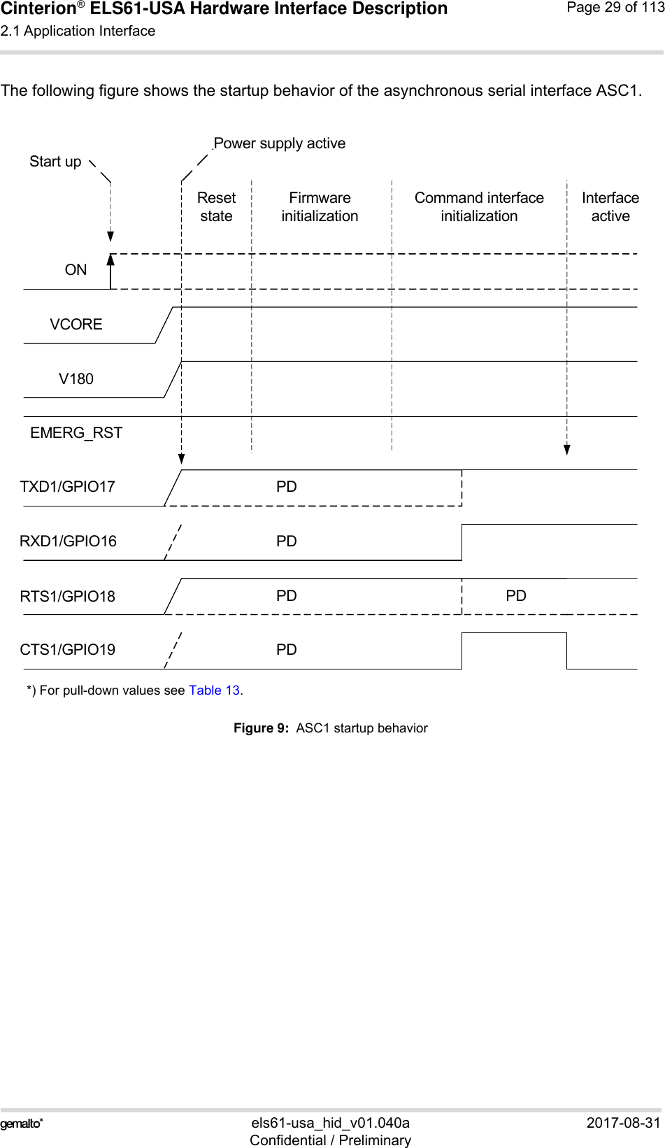
![Cinterion® ELS61-USA Hardware Interface Description2.1 Application Interface59els61-usa_hid_v01.040a 2017-08-31Confidential / PreliminaryPage 28 of 1132.1.5 Serial Interface ASC1Four ELS61-USA GPIO lines can be configured as ASC1 interface signals to provide a 4-wire unbalanced, asynchronous modem interface ASC1 conforming to ITU-T V.24 protocol DCE signalling. The electrical characteristics do not comply with ITU-T V.28. The significant levels are 0V (for low data bit or active state) and 1.8V (for high data bit or inactive state). For electrical characteristics please refer to Table 2. For an illustration of the interface line’s startup behavior see Figure 9. The ASC1 interface lines are originally available as GPIO lines. If configured as ASC1 lines, the GPIO lines are assigned as follows: GPIO16 --> RXD1, GPIO17 --> TXD1, GPIO18 --> RTS1 and GPIO19 --> CTS1. Configuration is done by AT command (see [1]: AT^SCFG). The configuration is non-volatile and becomes active after a module restart.ELS61-USA is designed for use as a DCE. Based on the conventions for DCE-DTE connec-tions it communicates with the customer application (DTE) using the following signals:• Port TXD @ application sends data to module’s TXD1 signal line• Port RXD @ application receives data from the module’s RXD1 signal lineFigure 8: Serial interface ASC1Features• Includes only the data lines TXD1 and RXD1 plus RTS1 and CTS1 for hardware hand-shake. • On ASC1 no RING line is available.• Configured for 8 data bits, no parity and 1 or 2 stop bits.• ASC1 can be operated at fixed bit rates from 1,200 bps to 921,600 bps. • Autobauding supports bit rates from 1,200bps up to 230,400bps. • Supports RTS1/CTS1 hardware flow. The hardware hand shake line RTS0 has an internalpull down resistor causing a low level signal, if the line is not used and open. Although hard-ware flow control is recommended, this allows communication by using only RXD and TXDlines.](https://usermanual.wiki/THALES-DIS-AlS-Deutschland/ELS61-USA/User-Guide-3601224-Page-28.png)
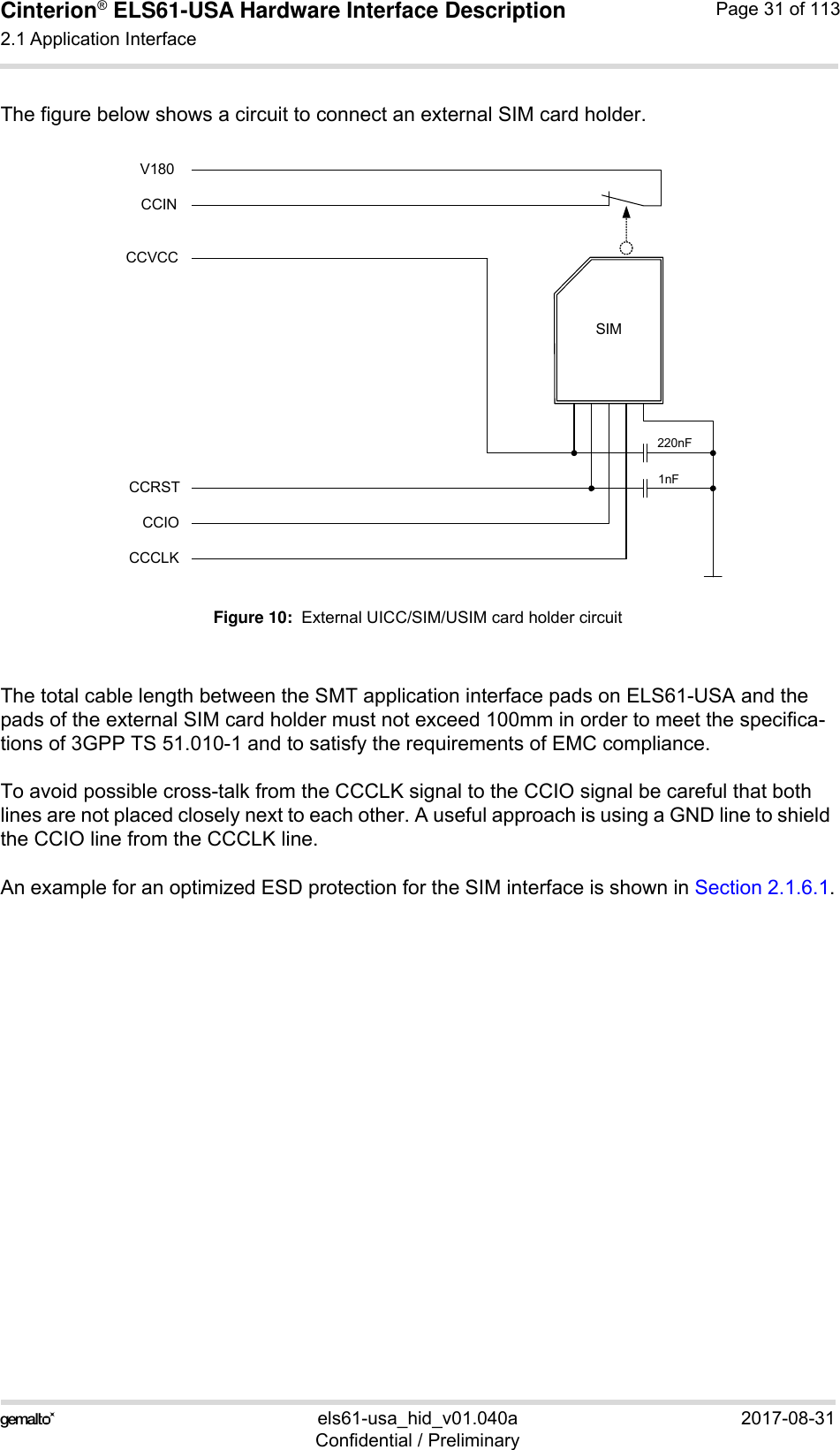
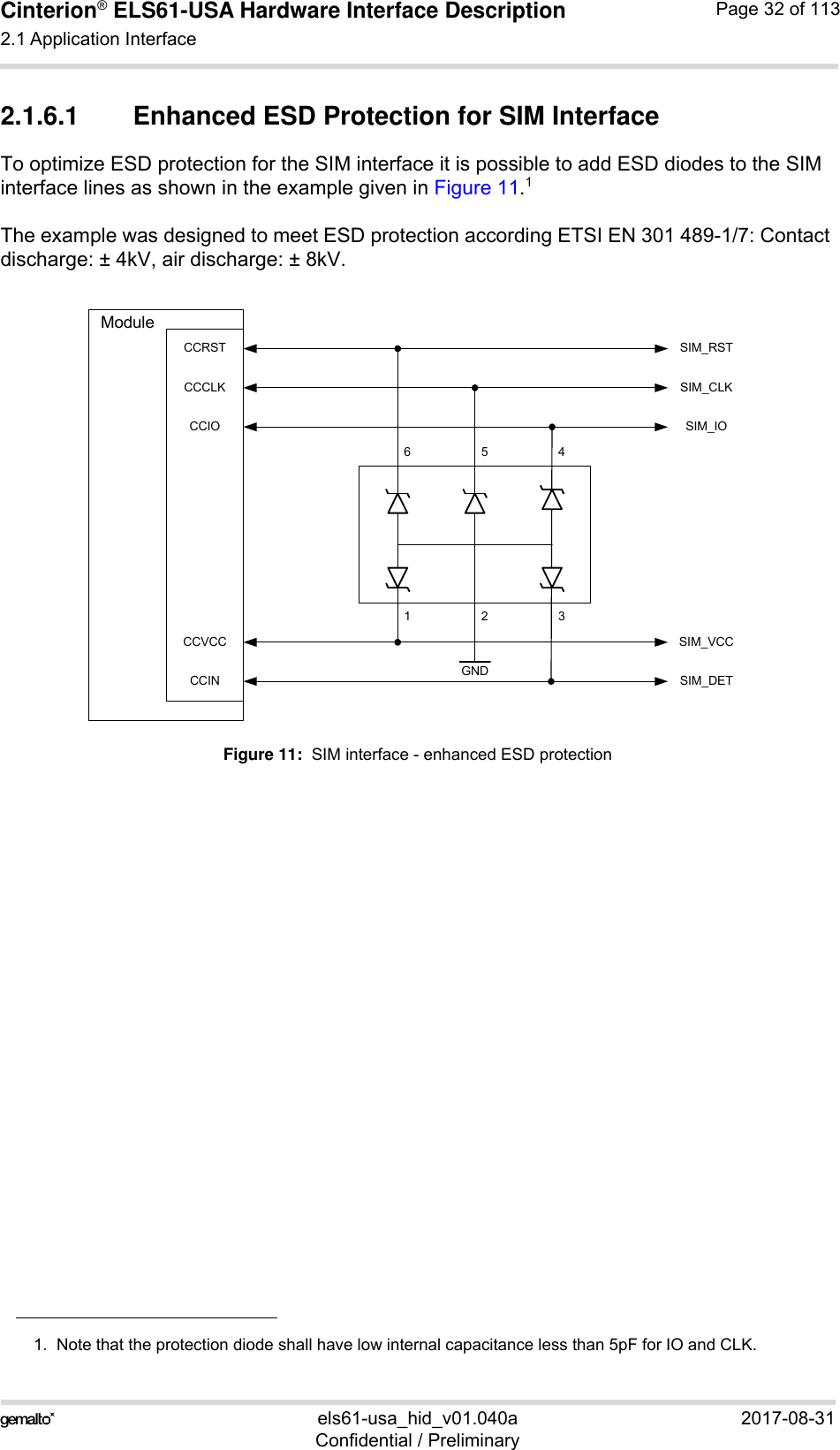
![Cinterion® ELS61-USA Hardware Interface Description2.1 Application Interface59els61-usa_hid_v01.040a 2017-08-31Confidential / PreliminaryPage 30 of 1132.1.6 UICC/SIM/USIM InterfaceELS61-USA has an integrated UICC/SIM/USIM interface compatible with the 3GPP 31.102 and ETSI 102 221. This is wired to the host interface in order to be connected to an external SIM card holder. Five pads on the SMT application interface are reserved for the SIM interface. The UICC/SIM/USIM interface supports 3V and 1.8V SIM cards. Please refer to Table 2 for electrical specifications of the UICC/SIM/USIM interface lines depending on whether a 3V or 1.8V SIM card is used.The CCIN signal serves to detect whether a tray (with SIM card) is present in the card holder. To take advantage of this feature, an appropriate SIM card detect switch is required on the card holder. For example, this is true for the model supplied by Molex, which has been tested to op-erate with ELS61-USA and is part of the Gemalto M2M reference equipment submitted for type approval. See Section 7.1 for Molex ordering numbers.Note [1]: No guarantee can be given, nor any liability accepted, if loss of data is encountered after removing the SIM card during operation. Also, no guarantee can be given for properly initializing any SIM card that the user inserts after having removed the SIM card during operation. In this case, the application must restart ELS61-USA.Note [2]: On the evaluation board, the CCIN signal is inverted, thus the CCIN signal is by default high and will change to a low level if a SIM card is inserted. Table 4: Signals of the SIM interface (SMT application interface)Signal DescriptionGND Separate ground connection for SIM card to improve EMC.CCCLK Chipcard clockCCVCC SIM supply voltage.CCIO Serial data line, input and output.CCRST Chipcard resetCCIN Input on the baseband processor for detecting a SIM card tray in the holder. If the SIM is removed during operation the SIM interface is shut down immediately to prevent destruc-tion of the SIM. The CCIN signal is by default low and will change to high level if a SIM card is inserted.The CCIN signal is mandatory for applications that allow the user to remove the SIM card during operation. The CCIN signal is solely intended for use with a SIM card. It must not be used for any other purposes. Failure to comply with this requirement may invalidate the type approval of ELS61-USA.](https://usermanual.wiki/THALES-DIS-AlS-Deutschland/ELS61-USA/User-Guide-3601224-Page-30.png)
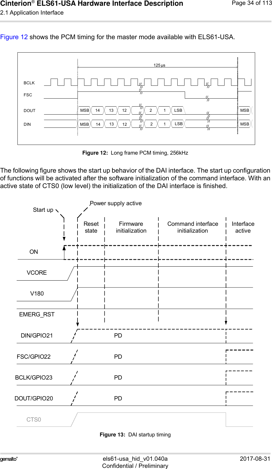
![Cinterion® ELS61-USA Hardware Interface Description2.1 Application Interface59els61-usa_hid_v01.040a 2017-08-31Confidential / PreliminaryPage 33 of 1132.1.7 Digital Audio Interface (DAI)ELS61-USA supports a digital audio interface that can be employed either as pulse code mod-ulation interface (see Section 2.1.7.1) or as inter IC sound interface (see Section 2.1.7.2). Op-eration of these interface variants is mutually exclusive, and can be configured by AT command (AT^SAIC; see [1]).2.1.7.1 Pulse Code Modulation Interface (PCM)Four ELS61-USA GPIO lines can be configured as pule code modulation interface (PCM). ThePCM functionality allows for the use of an external codec like the W681360 (see Section2.1.7.3). The PCM interface supports the following features:• Master and Slave mode• Long frame and short frame• 8kHz sample rate / 125µs frame duration (narrow band), 16kHz sample rate / 62.5µs frameduration (wide band)• Bit clock: 256kHz (sample rate of 8kHz), 264kHz (short frame), 520kHz (sample rate of8kHz), 528kHz (short frame), 1040kHz (sample rate of 16kHz)• The most significant bit MSB is transferred first• Data write at rising edge / data read at falling edge• Common frame sync signal for transmit and receiveThe four GPIO lines can be configured as DAI/PCM interface signals as follows: GPIO20 -->DOUT, GPIO21--> DIN, GPIO22 --> FSC and GPIO23 --> BCLK. The configuration is done byAT command (see [1]). It is non-volatile and becomes active after a module restart. Table 5 de-scribes the available DAI/PCM lines at the digital audio interface. For electrical details see Sec-tion 2.1.2.Table 5: Overview of DAI/PCM linesSignal name Input/Output DescriptionDOUT O PCM data from ELS61-USA to external codec.DIN I PCM data from external codec to ELS61-USA.FSC O Frame synchronization signal to external codec:Long frame (8kHz)BCLK O Bit clock to external codec.](https://usermanual.wiki/THALES-DIS-AlS-Deutschland/ELS61-USA/User-Guide-3601224-Page-33.png)
![Cinterion® ELS61-USA Hardware Interface Description2.1 Application Interface59els61-usa_hid_v01.040a 2017-08-31Confidential / PreliminaryPage 35 of 1132.1.7.2 Inter IC Sound Interface The Inter IC Sound interface (I2S) is enabled using the AT command AT^SAIC (see [1]). An activation is possible only out of call and out of tone presentation. The I2S properties and capabilities comply with the requirements laid out in the Phillips I2S Bus Specifications, revised June 5, 1996.The I2S interface has the following characteristics:• Clock Modes: Master with permanent clock option • Sampling Rate: 8kHz (narrow band), 16kHz (wide band)• Bit clock: 512kHzThe digital audio interface pads available for the PCM interface are also available for the I2S interface. In I2S mode they have the same electrical characteristics (for more information on the DOUT, DIN, FSC and BCLK pads please refer to Section 2.1.2 and Section 2.1.7.1).The table below lists the available pads at the module’s digital audio interface.The following figure shows the I2S timing for the master mode available with the module.Figure 14: I2S timing, 8kHz sample rateTable 6: Overview of DAI/I2S linesSignal name Input/Output DescriptionDOUT O I2S data from module to external codec.DIN I I2S data from external codec to module.FSC O Frame synchronization signal to external codec: Word alignment (WS)BCLK O Bit clock to external codec: 512kHzBCLKDOUTDINFSCMSBMSBLSBLSB14 1314 1311121222MSBMSB125 µs](https://usermanual.wiki/THALES-DIS-AlS-Deutschland/ELS61-USA/User-Guide-3601224-Page-35.png)
![Cinterion® ELS61-USA Hardware Interface Description2.1 Application Interface59els61-usa_hid_v01.040a 2017-08-31Confidential / PreliminaryPage 37 of 1132.1.7.4 Electrical Characteristics of the Voiceband PartSetting Audio Parameters by AT CommandsThe audio modes 2 to 10 can be temporarily adjusted according to the AT command parameter listed in the table below. The audio parameter is set with the AT commandAT^SNFO and the audio mode is changed by AT^SNFS (see [1]). For a model of how the parameters influence the audio signal path see Section .Audio Programming ModelThe audio programming model shows how the signal path can be influenced by varying AT command parameters: . For more information on the AT commands and parameters see Sec-tion and [1].Figure 17: Audio programming model Table 7: Audio parameters adjustable by AT commandParameter Influence to Range Gain range CalculationAT^SNFIinVolStep Digital TX volume 01...100Mute-43.5…+6dB0.5dB steps(inVolStep-88)*0.5dB88 = 0dB (default)AT^SNFOoutVolStep Digital RX volume 01…100Mute-43.5…+6dB0.5dB steps(outVolStep-88)*0.5dB88 = 0dB (default)sideToneStep Sidetone gain11. The sidetone path contains two logically gain cells in series as shown in Figure 17. The first one can be controlled by the parameter sideToneGain while the second one will be controlled by outVolStep to keep the resulting sidetone gain constant independently of the RX Volume. The second cell introduces an off-set of -37.5dB to the sidetone path. The resulting sidetone gain can be calculated according the following formula:Resulting sidetone gain = 0.5 * (sideToneStep - outVolStep) -37.5 [dB]If sideToneStep = 0 the sidetone path is completely muted - independent of outVolStep.00...175Mute-43.5...43.5dB0.5dB stepsSideToneStep*0.5dB88 = 0dBSignal Processing / Speech coder+AT parameters are given in brackets <...> and marked red and italic .<outVolStep><inVolStep>Speech decoder / Signal ProcessingDAI4PCM/I2S<sideToneGain>](https://usermanual.wiki/THALES-DIS-AlS-Deutschland/ELS61-USA/User-Guide-3601224-Page-37.png)
![Cinterion® ELS61-USA Hardware Interface Description2.1 Application Interface59els61-usa_hid_v01.040a 2017-08-31Confidential / PreliminaryPage 40 of 1132.1.9 GPIO InterfaceELS61-USA offers a GPIO interface with 22 GPIO lines. The GPIO lines are shared with otherinterfaces or functions: Fast shutdown (see Section 2.1.14.4), status LED (see Section2.1.14.1), the PWM functionality (see Section 2.1.12), an pulse counter (see Section 2.1.13),ASC0 (see Section 2.1.4), ASC1 (see Section 2.1.5), an SPI interface (see Section 2.1.11), anda DAI interface (see Section 2.1.7). The following table shows the configuration variants for the GPIO pads. All variants are mutu-ally exclusive, i.e. a pad configured for instance as Status LED is locked for alternative usage.After startup, the above mentioned alternative GPIO line assignments can be configured usingAT commands (see [1]). The configuration is non-volatile and available after module restart.Table 8: GPIO lines and possible alternative assignmentGPIO Fast Shutdown Status LED PWM Pulse Counter ASC0 ASC1 SPI DAIGPIO1 DTR0GPIO2 DCD0GPIO3 DSR0 SPI_CLKGPIO4 FST_SHDNGPIO5 Status LEDGPIO6 PWM2GPIO7 PWM1GPIO8 COUNTERGPIO11GPIO12GPIO13GPIO14GPIO15GPIO16 RXD1 MOSIGPIO17 TXD1 MISOGPIO18 RTS1GPIO19 CTS1 SPI_CSGPIO20 DOUTGPIO21 DINGPIO22 FSCGPIO23 BCLKGPIO24 RING0](https://usermanual.wiki/THALES-DIS-AlS-Deutschland/ELS61-USA/User-Guide-3601224-Page-40.png)
![Cinterion® ELS61-USA Hardware Interface Description2.1 Application Interface59els61-usa_hid_v01.040a 2017-08-31Confidential / PreliminaryPage 42 of 1132.1.10 I2C InterfaceI2C is a serial, 8-bit oriented data transfer bus for bit rates up to 400kbps in Fast mode. It con-sists of two lines, the serial data line I2CDAT and the serial clock line I2CCLK. The module actsas a single master device, e.g. the clock I2CCLK is driven by the module. I2CDAT is a bi-direc-tional line. Each device connected to the bus is software addressable by a unique 7-bit ad-dress, and simple master/slave relationships exist at all times. The module operates as master-transmitter or as master-receiver. The customer application transmits or receives data only onrequest of the module.To configure and activate the I2C bus use the AT^SSPI command. Detailed information on theAT^SSPI command as well explanations on the protocol and syntax required for data transmis-sion can be found in [1].The I2C interface can be powered via the V180 line of ELS61-USA. If connected to the V180line, the I2C interface will properly shut down when the module enters the Power Down mode.In the application I2CDAT and I2CCLK lines need to be connected to a positive supply voltagevia a pull-up resistor. For electrical characteristics please refer to Table 2.Figure 20: I2C interface connected to V180Note: Good care should be taken when creating the PCB layout of the host application: Thetraces of I2CCLK and I2CDAT should be equal in length and as short as possible.I2CCLKI2CDATGNDI2CCLKI2CDATGNDModule ApplicationV180R pull upR pull upR pull upR pull up1KOhm1KOhm](https://usermanual.wiki/THALES-DIS-AlS-Deutschland/ELS61-USA/User-Guide-3601224-Page-42.png)
![Cinterion® ELS61-USA Hardware Interface Description2.1 Application Interface59els61-usa_hid_v01.040a 2017-08-31Confidential / PreliminaryPage 44 of 1132.1.11 SPI InterfaceFour ELS61-USA GPIO interface lines can be configured as Serial Peripheral Interface (SPI).The SPI is a synchronous serial interface for control and data transfer between ELS61-USAand the external application. Only one application can be connected to the SPI and the inter-face supports only master mode. The transmission rates are up to 6.5Mbit/s. The SPI interfacecomprises the two data lines MOSI and MISO, the clock line SPI_CLK a well as the chip selectline SPI_CS.The four GPIO lines can be configured as SPI interface signals as follows: GPIO3 --> SPI_CLK, GPIO16 --> MOSI, GPIO17 --> MISO and GPIO19 --> SPI_CS. The configuration is done by AT command (see [1]). It is non-volatile and becomes active after a module restart.The GPIO lines are also shared with the ASC1 signal lines and the ASC0 modem status signal line DSR0.To configure and activate the SPI interface use the AT^SSPI command. Detailed informationon the AT^SSPI command as well explanations on the SPI modes required for data transmis-sion can be found in [1].In general, SPI supports four operation modes. The modes are different in clock phase andclock polarity. The module’s SPI mode can be configured by using the AT command AT^SSPI.Make sure the module and the connected slave device works with the same SPI mode.Figure 22 shows the characteristics of the four SPI modes. The SPI modes 0 and 3 are the mostcommon used modes. For electrical characteristics please refer to Table 2.Figure 22: Characteristics of SPI modesSPI MODE 0 SPI MODE 1SPI MODE 2 SPI MODE 3Clock phaseClock polaritySPI_CSMOSISPI_CLKMISOSPI_CSMOSISPI_CLKMISOSPI_CSMOSISPI_CLKMISOSPI_CSMOSISPI_CLKMISOSample SampleSample Sample](https://usermanual.wiki/THALES-DIS-AlS-Deutschland/ELS61-USA/User-Guide-3601224-Page-44.png)
![Cinterion® ELS61-USA Hardware Interface Description2.1 Application Interface59els61-usa_hid_v01.040a 2017-08-31Confidential / PreliminaryPage 46 of 1132.1.14.2 Power Indication CircuitIn Power Down mode the maximum voltage at any digital or analog interface line must not ex-ceed +0.3V (see also Section 2.1.2.1). Exceeding this limit for any length of time might causepermanent damage to the module. It is therefore recommended to implement a power indication signal that reports the module’spower state and shows whether it is active or in Power Down mode. While the module is inPower Down mode all signals with a high level from an external application need to be set tolow state or high impedance state. The sample power indication circuit illustrated in Figure 24denotes the module’s active state with a low signal and the module’s Power Down mode witha high signal or high impedance state.Figure 24: Power indication circuit2.1.14.3 Host WakeupIf no call, data or message transfer is in progress, the host may shut down its own USB inter-face to save power. If a call or other request (URC’s, messages) arrives, the host can be noti-fied of these events and be woken up again by a state transition of the ASC0 interface‘s RING0line. This functionality should only be used with legacy USB applications not supporting the rec-ommended USB suspend and resume mechanism as described in [5] (see also Section 2.1.3.1).For more information on how to configure the RING0 line by AT^SCFG command see [1].Possible RING0 line states are listed in Table 9.Table 9: Host wakeup linesSignal I/O DescriptionRING0 O Inactive to active low transition:0 = The host shall wake up1 = No wake up request 22k10k100k100k4.7kV180VCOREPower indicationExternal power supply](https://usermanual.wiki/THALES-DIS-AlS-Deutschland/ELS61-USA/User-Guide-3601224-Page-46.png)
![Cinterion® ELS61-USA Hardware Interface Description2.1 Application Interface59els61-usa_hid_v01.040a 2017-08-31Confidential / PreliminaryPage 47 of 1132.1.14.4 Fast ShutdownThe GPIO4 interface line can be configured as fast shutdown signal line FST_SHDN. The con-figured FST_SHDN line is an active low control signal and must be applied for at least 1 milli-seconds. If unused this line can be left open because of a configured internal pull-up resistor. Before setting the FST_SHDN line to low, the ON signal should be set to low (see Figure 25). Otherwise there might be back powering at the ON line in Power Down mode.The fast shutdown feature can be triggered using the AT command AT^SMSO=<fso>. For de-tails see [1].If triggered, a low impulse >1 milliseconds on the FST_SHDN line starts the fast shutdown. The fast shutdown procedure still finishes any data activities on the module's flash file system, thus ensuring data integrity, but will no longer deregister gracefully from the network, thus saving the time required for network deregistration.Figure 25: Fast shutdown timingPlease note that the normal software controlled shutdown using AT^SMSO will allow option for a fast shutdown by parameter <fso>, i.e., without network deregistration. However, in this case no URCs including shutdown URCs will be provided by the AT^SMSO command.Please also note that the fast shutdown operation does not allow the module deregister from the network, therefore, this practice is not recommended, and should not be conducted on reg-ular basis. If it is used for energy saving reason, for instance, used in battery-driven solutions that require prompt system shutdown before battery depletion, discretion is advised in such case. BATT+VCOREV180VDDLPFast shut down procedure Power downEMERG_RSTONGPIO4/FST_SHDN<15ms_](https://usermanual.wiki/THALES-DIS-AlS-Deutschland/ELS61-USA/User-Guide-3601224-Page-47.png)
![Cinterion® ELS61-USA Hardware Interface Description2.2 RF Antenna Interface59els61-usa_hid_v01.040a 2017-08-31Confidential / PreliminaryPage 48 of 1132.2 RF Antenna InterfaceThe ELS61-USA UMTS/LTE antenna interface comprises a UMTS/LTE main antenna as well as a UMTS/LTE Rx diversity antenna to improve signal reliability and quality1. The RF interface has an impedance of 50. ELS61-USA is capable of sustaining a total mismatch at the antenna line without any damage, even when transmitting at maximum RF power.The external antenna must be matched properly to achieve best performance regarding radi-ated power, modulation accuracy and harmonic suppression. Antenna matching networks are not included on the ELS61-USA module and should be placed in the host application if the an-tenna does not have an impedance of 50.Regarding the return loss ELS61-USA provides the following values in the active band:2.2.1 Antenna Interface SpecificationsFor approval reasons it is mandatory to connect/apply the Rx diversity antenna to an existing antenna. Not connecting/applying the Rx diversity antenna does not necessarily impact the performance, but may result in approval failures. The minimum antenna efficiency should be better than 50%. 1. By delivery default the UMTS/LTE Rx diversity antenna is configured as available for the module sinceits usage is mandatory for LTE. Please refer to [1] for details on how to configure antenna settings.Table 10: Return loss in the active bandState of module Return loss of module Recommended return loss of applicationReceive > 8dB > 12dBTransmit not applicable > 12dBTable 11: RF Antenna interface UMTS/LTE (at operating temperature range1)Parameter Conditions Min. Typical Max. UnitLTE connectivity2Band 2, 4, 5,12Receiver Input Sensitivity @ARP (Dual Antenna; ch. bandwidth 5MHz)LTE 700 Band 12 (ch. band-width 5MHz)-97 -103.5 dBmLTE 850 Band 5 (ch. band-width 10MHz)-98 -104.5 dBmLTE AWS Band 4 (ch. band-width 10MHz)-100 -103 dBmLTE 1900 Band 2 (ch. band-width 10MHz) -98 -102.5 dBm](https://usermanual.wiki/THALES-DIS-AlS-Deutschland/ELS61-USA/User-Guide-3601224-Page-48.png)
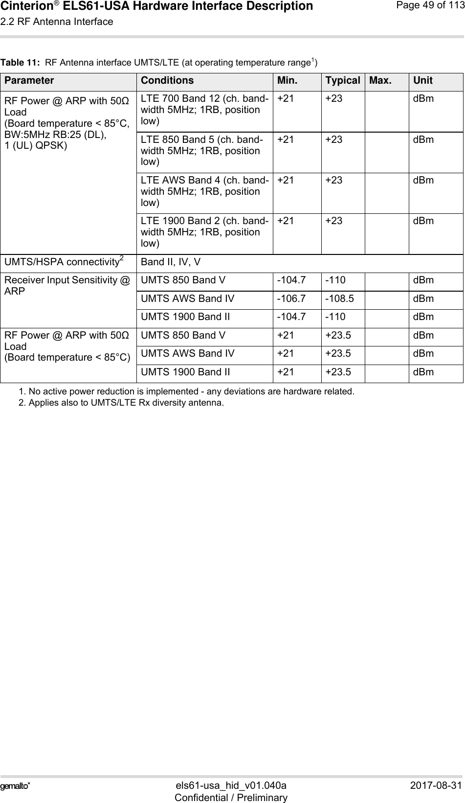
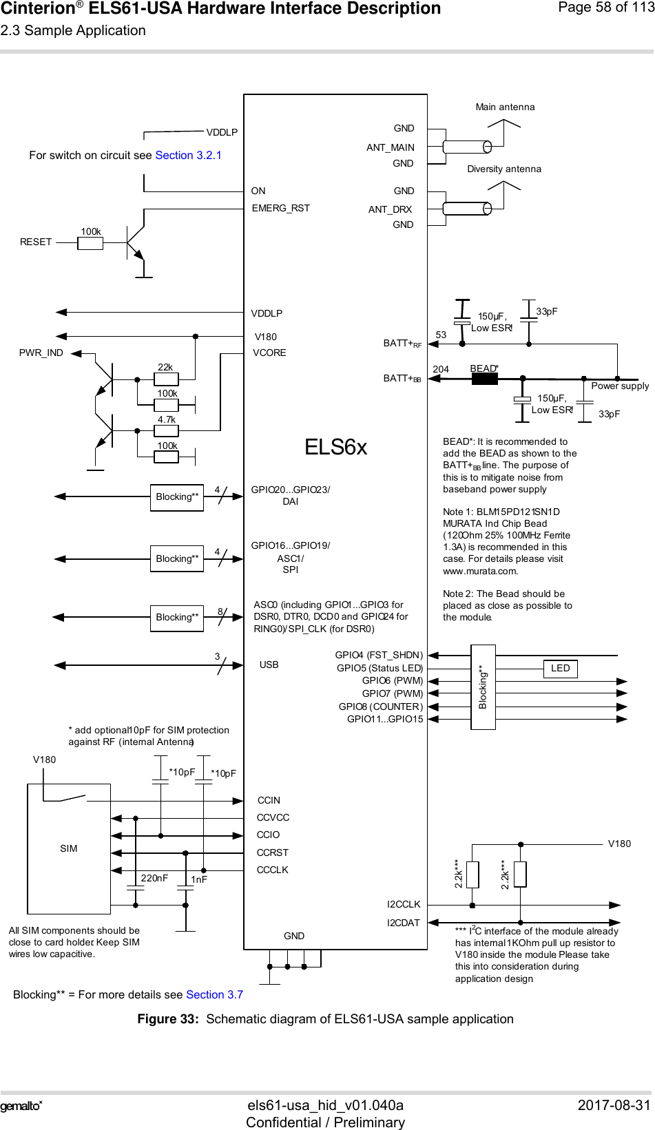
![Cinterion® ELS61-USA Hardware Interface Description2.3 Sample Application59els61-usa_hid_v01.040a 2017-08-31Confidential / PreliminaryPage 57 of 1132.3 Sample ApplicationFigure 33 shows a typical example of how to integrate a ELS61-USA module with an applica-tion. Usage of the various host interfaces depends on the desired features of the application.Because of the very low power consumption design, current flowing from any other source intothe module circuit must be avoided, for example reverse current from high state external controllines. Therefore, the controlling application must be designed to prevent reverse current flow.Otherwise there is the risk of undefined states of the module during startup and shutdown oreven of damaging the module.Because of the high RF field density inside the module, it cannot be guaranteed that no selfinterference might occur, depending on frequency and the applications grounding concept. Thepotential interferers may be minimized by placing small capacitors (47pF) at suspected lines(e.g. RXD0, VDDLP, and ON). While developing SMT applications it is strongly recommended to provide test pointsfor certain signals, i.e., lines to and from the module - for debug and/or test purposes.The SMT application should allow for an easy access to these signals. For details onhow to implement test points see [3].The EMC measures are best practice recommendations. In fact, an adequate EMC strategy foran individual application is very much determined by the overall layout and, especially, the po-sition of components. Depending on the micro controller used by an external application ELS61-USA‘s digital input and output lines may require level conversion. Section 2.3.1 shows a possible sample level conversion circuit.Note: ELS61-USA is not intended for use with cables longer than 3m.DisclaimerNo warranty, either stated or implied, is provided on the sample schematic diagram shown inFigure 33 and the information detailed in this section. As functionality and compliance with na-tional regulations depend to a great amount on the used electronic components and the indi-vidual application layout manufacturers are required to ensure adequate design and operatingsafeguards for their products using ELS61-USA modules.](https://usermanual.wiki/THALES-DIS-AlS-Deutschland/ELS61-USA/User-Guide-3601224-Page-57.png)
![Cinterion® ELS61-USA Hardware Interface Description3 Operating Characteristics83els61-usa_hid_v01.040a 2017-08-31Confidential / PreliminaryPage 60 of 1133 Operating Characteristics3.1 Operating ModesThe table below briefly summarizes the various operating modes referred to throughout the document.Table 12: Overview of operating modesMode FunctionNormal operationUMTS / HSPA / LTE SLEEPPower saving set automatically when no call is in progress and the USB connection is suspended by host or not present and no active commu-nication via ASC0. UMTS / HSPA / LTE IDLEPower saving disabled or an USB connection not suspended, but no call in progress.UMTS TALK/UMTS DATAUMTS data transfer in progress. Power consumption depends on net-work settings (e.g. TPC Pattern) and data transfer rate.HSPA DATA HSPA data transfer in progress. Power consumption depends on net-work settings (e.g. TPC Pattern) and data transfer rate.LTE DATA LTE data transfer in progress. Power consumption depends on network settings (e.g. TPC Pattern) and data transfer rate.Power DownNormal shutdown after sending the power down command. Only a voltage regulator is active for powering the RTC. Software is not active. Interfaces are not accessible. Operat-ing voltage remains applied.Airplane modeAirplane mode shuts down the radio part of the module, causes the module to log off from the network and disables all AT commands whose execution requires a radio connection.Airplane mode can be controlled by AT command (see [1]).Alarm modeRestricted operation launched by RTC alert function when the module is in Power Down mode. In Alarm mode, the module remains deregistered from the network. Limited number of AT commands is accessible.](https://usermanual.wiki/THALES-DIS-AlS-Deutschland/ELS61-USA/User-Guide-3601224-Page-60.png)
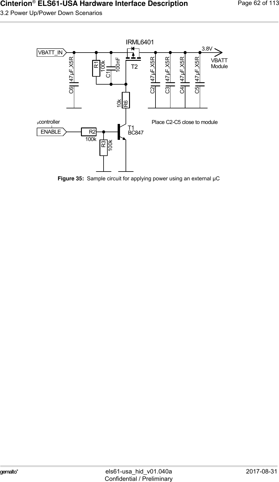
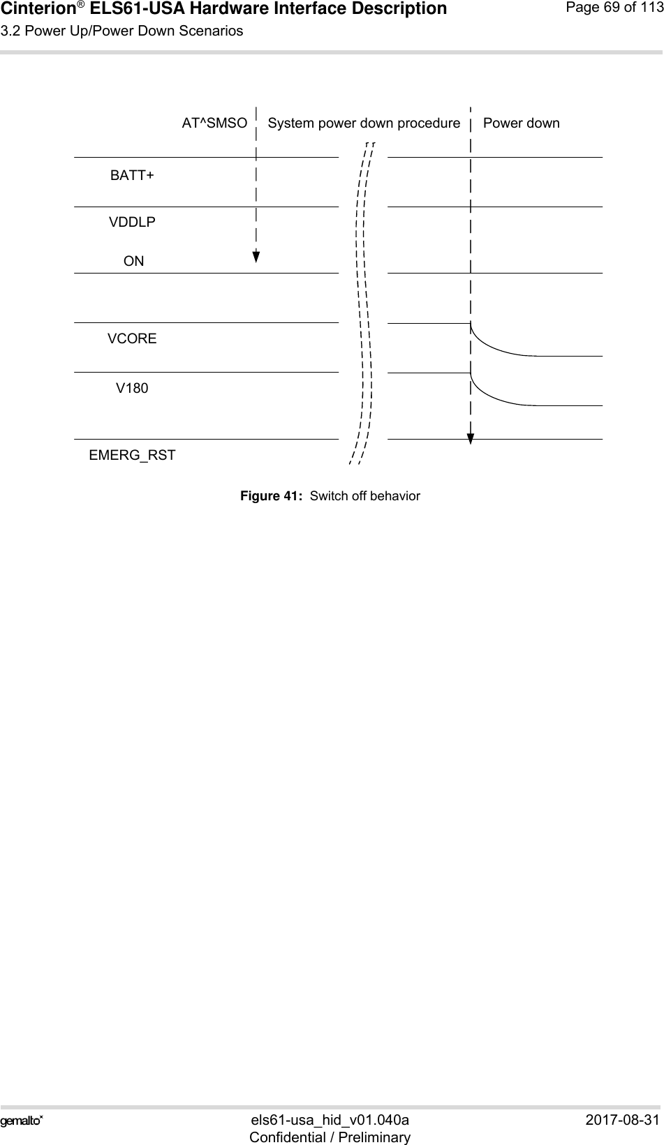
![Cinterion® ELS61-USA Hardware Interface Description3.2 Power Up/Power Down Scenarios83els61-usa_hid_v01.040a 2017-08-31Confidential / PreliminaryPage 61 of 1133.2 Power Up/Power Down ScenariosIn general, be sure not to turn on ELS61-USA while it is beyond the safety limits of voltage and temperature stated in Section 2.1.2.1. ELS61-USA immediately switches off after having start-ed and detected these inappropriate conditions. In extreme cases this can cause permanent damage to the module. 3.2.1 Turn on ELS61-USAELS61-USA can be turned on as described in the following sections:• Connecting the operating voltage BATT+ (see Section 3.2.1.1).• Hardware driven switch on by ON line: Starts Normal mode (see Section 3.2.1.2).After startup or restart, the module will send the URC ^SYSSTART that notifies the host appli-cation that the first AT command can be sent to the module (see also [1]).3.2.1.1 Connecting ELS61-USA BATT+ LinesFigure 35 shows sample external application circuits that allow to connect (and also to tempo-rarily disconnect) the module‘s BATT+ lines from the external application‘s power supply. Figure 35 illustrates the application of power employing an externally controlled microcontrol-ler. The voltage supervisory circuit ensures that the power is disconnected and applied againdepending on given thresholds.The transistor T2 mentioned in Figure 35 should have an RDS_ON value < 50m in order to min-imize voltage drops. Such circuits could be useful to maximize power savings for battery driven applications or tocompletely switch off and restart the module after a firmware update.After connecting the BATT+ lines the module can then be (re-)started as described in Section3.2.1.2 and Section 3.2.2.](https://usermanual.wiki/THALES-DIS-AlS-Deutschland/ELS61-USA/User-Guide-3601224-Page-61.png)
![Cinterion® ELS61-USA Hardware Interface Description3.2 Power Up/Power Down Scenarios83els61-usa_hid_v01.040a 2017-08-31Confidential / PreliminaryPage 65 of 113Figure 39: Automatic ON circuit based on voltage detector - option 23.2.2 Restart ELS61-USA After startup ELS61-USA can be re-started as described in the following sections:• Software controlled reset by AT+CFUN command: Starts Normal mode (see Section3.2.2.1).• Hardware controlled reset by EMERG_RST line: Starts Normal mode (see Section 3.2.2.2).3.2.2.1 Restart ELS61-USA via AT+CFUN CommandTo reset and restart the ELS61-USA module use the command AT+CFUN. See [1] for details. Voltage Detector*BATT+BBGNDONVDDLP* It is recommended to apply the ultra-low current voltage detector NCP303LSN28T1 manufactured by ON Semiconductor. Details please refer to www.onsemi.comInput RESETOutputGNDR110KOhm2130.1μFGND 5 CD](https://usermanual.wiki/THALES-DIS-AlS-Deutschland/ELS61-USA/User-Guide-3601224-Page-65.png)
![Cinterion® ELS61-USA Hardware Interface Description3.2 Power Up/Power Down Scenarios83els61-usa_hid_v01.040a 2017-08-31Confidential / PreliminaryPage 70 of 1133.2.5 Automatic ShutdownAutomatic shutdown takes effect if the following event occurs:• ELS61-USA board is exceeding the critical limits of overtemperature or undertemperature(see Section 3.2.5.1)• Undervoltage or overvoltage is detected (see Section 3.2.5.2 and Section 3.2.5.3)The automatic shutdown procedure is equivalent to the power-down initiated with an AT com-mand, i.e. ELS61-USA logs off from the network and the software enters a secure state avoid-ing loss of data. 3.2.5.1 Thermal ShutdownThe board temperature is constantly monitored by an internal NTC resistor located on the PCB.The values detected by the NTC resistor are measured directly on the board and therefore, arenot fully identical with the ambient temperature. Each time the board temperature goes out of range or back to normal, ELS61-USA instantlydisplays an alert (if enabled).• URCs indicating the level "1" or "-1" allow the user to take appropriate precautions, such asprotecting the module from exposure to extreme conditions. The presentation of the URCsdepends on the settings selected with the AT^SCTM write command (for details see [1]):AT^SCTM=1: Presentation of URCs is always enabled. AT^SCTM=0 (default): Presentation of URCs is enabled during the 2 minute guard periodafter start-up of ELS61-USA. After expiry of the 2 minute guard period, the presentation ofURCs will be disabled, i.e. no URCs with alert levels "1" or ''-1" will be generated.• URCs indicating the level "2" or "-2" are instantly followed by an orderly shutdown. The pre-sentation of these URCs is always enabled, i.e. they will be output even though the factorysetting AT^SCTM=0 was never changed.The maximum temperature ratings are stated in Section 3.5. Refer to Table 14 for the associ-ated URCs. Table 14: Temperature dependent behaviorSending temperature alert (2min after ELS61-USA start-up, otherwise only if URC presentation enabled)^SCTM_B: 1 Board close to overtemperature limit.^SCTM_B: -1 Board close to undertemperature limit.^SCTM_B: 0 Board back to non-critical temperature range.Automatic shutdown (URC appears no matter whether or not presentation was enabled)^SCTM_B: 2 Alert: Board equal or beyond overtemperature limit. ELS61-USA switches off.^SCTM_B: -2 Alert: Board equal or below undertemperature limit. ELS61-USA switches off.](https://usermanual.wiki/THALES-DIS-AlS-Deutschland/ELS61-USA/User-Guide-3601224-Page-70.png)
![Cinterion® ELS61-USA Hardware Interface Description3.2 Power Up/Power Down Scenarios83els61-usa_hid_v01.040a 2017-08-31Confidential / PreliminaryPage 71 of 1133.2.5.2 Undervoltage ShutdownThe undervoltage shutdown threshold is the specified minimum supply voltage VBATT+ given inTable 2. When the average supply voltage measured by ELS61-USA approaches the under-voltage shutdown threshold (i.e., 0.05V offset) the module will send the following URC: ^SBC: Undervoltage WarningThe undervoltage warning is sent only once - until the next time the module is close to the un-dervoltage shutdown threshold. If the voltage continues to drop below the specified undervoltage shutdown threshold, the mod-ule will send the following URC:^SBC: Undervoltage ShutdownThis alert is sent only once before the module shuts down cleanly without sending any furthermessages.This type of URC does not need to be activated by the user. It will be output automatically whenfault conditions occur.Note: For battery powered applications it is strongly recommended to implement a BATT+ con-necting circuit as described in Section 3.2.1.1 in order to not only be able save power, but alsoto restart the module after an undervoltage shutdown where the battery is deeply discharged.Also note that the undervoltage threshold is calculated for max. 400mV voltage drops duringtransmit burst. Power supply sources for external applications should be designed to tolerate400mV voltage drops without crossing the lower limit of 3.0 V. For external applications oper-ating at the limit of the allowed tolerance the default undervoltage threshold may be adaptedby subtracting an offset. For details see [1]: AT^SCFG= "MEShutdown/sVsup/threshold".3.2.5.3 Overvoltage ShutdownThe overvoltage shutdown threshold is the specified maximum supply voltage VBATT+ given inTable 2. When the average supply voltage measured by ELS61-USA approaches the overvolt-age shutdown threshold (i.e., 0.05V offset) the module will send the following URC:^SBC: Overvoltage WarningThe overvoltage warning is sent only once - until the next time the module is close to the over-voltage shutdown threshold. If the voltage continues to rise above the specified overvoltage shutdown threshold, the modulewill send the following URC:^SBC: Overvoltage ShutdownThis alert is sent only once before the module shuts down cleanly without sending any furthermessages.This type of URC does not need to be activated by the user. It will be output automatically whenfault conditions occur.Keep in mind that several ELS61-USA components are directly linked to BATT+ and, therefore,the supply voltage remains applied at major parts of ELS61-USA. Especially the power ampli-fier linked to BATT+RF is very sensitive to high voltage and might even be destroyed.](https://usermanual.wiki/THALES-DIS-AlS-Deutschland/ELS61-USA/User-Guide-3601224-Page-71.png)
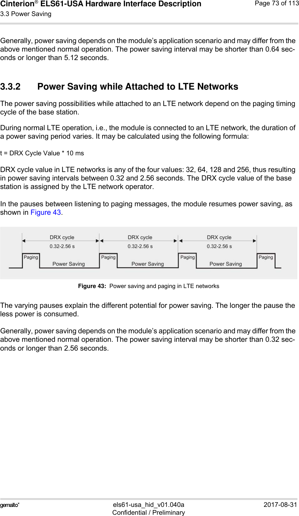
![Cinterion® ELS61-USA Hardware Interface Description3.3 Power Saving83els61-usa_hid_v01.040a 2017-08-31Confidential / PreliminaryPage 72 of 1133.3 Power SavingELS61-USA can be configured to control power consumption:• Using the AT command AT^SPOW it is possible to specify a so-called power saving modefor the module (<mode> = 2; for details on the command see [1]). The module‘s UART inter-faces (ASC0 and ASC1) are then deactivated and will only periodically be activated to beable to listen to network paging messages as described in Section 3.3.1 and Section 3.3.2.See Section 3.3.3 for a description on how to immediately wake up ELS61-USA again usingRTS0.Please note that the AT^SPOW setting has no effect on the USB interface. As long as theUSB connection is active, the module will not change into its SLEEP state to reduce its func-tionality to a minimum and thus minimizing its current consumption. To enable switchinginto SLEEP mode, the USB connection must therefore either not be present at all or theUSB host must bring its USB interface into Suspend state. Also, VUSB_IN should alwaysbe kept enabled for this functionality. See “Universal Serial Bus Specification Revision 2.0”1for a description of the Suspend state. 3.3.1 Power Saving while Attached to WCDMA NetworksThe power saving possibilities while attached to a WCDMA network depend on the paging tim-ing cycle of the base station. During normal WCDMA operation, i.e., the module is connected to a WCDMA network, the duration of a power saving period varies. It may be calculated using the following formula:t = 2DRX value * 10 ms (WCDMA frame duration). DRX (Discontinuous Reception) in WCDMA networks is a value between 6 and 9, thus result-ing in power saving intervals between 0.64 and 5.12 seconds. The DRX value of the base sta-tion is assigned by the WCDMA network operator. In the pauses between listening to paging messages, the module resumes power saving, as shown in Figure 42. Figure 42: Power saving and paging in WCDMA networksThe varying pauses explain the different potential for power saving. The longer the pause the less power is consumed.1. The specification is ready for download on http://www.usb.org/developers/docs/](https://usermanual.wiki/THALES-DIS-AlS-Deutschland/ELS61-USA/User-Guide-3601224-Page-72.png)
![Cinterion® ELS61-USA Hardware Interface Description3.5 Operating Temperatures83els61-usa_hid_v01.040a 2017-08-31Confidential / PreliminaryPage 79 of 1133.5 Operating TemperaturesPlease note that the module’s lifetime, i.e., the MTTF (mean time to failure) may be reduced, if operated outside the extended temperature range. See also Section 3.2.5 for information about the NTC for on-board temperature measurement,automatic thermal shutdown and alert messages.Note: Within the specified operating temperature ranges the board temperature may vary to agreat extent depending on operating mode, used frequency band, radio output power and cur-rent supply voltage. For more information regarding the module’s thermal behavior please refer to [4].Table 17: Board temperatureParameter Min Typ Max UnitNormal operation -30 +25 +85 °CExtended operation11. Extended operation allows normal mode speech calls or data transmission for limited time until automatic thermal shutdown takes effect. Within the extended temperature range (outside the normal operating temperature range) the specified electrical characteristics may be in- or decreased.-40 +90 °CAutomatic shutdown2Temperature measured on ELS61-USAboard2. Due to temperature measurement uncertainty, a tolerance of ±3°C on the thresholds may occur.<-40 --- >+90 °C](https://usermanual.wiki/THALES-DIS-AlS-Deutschland/ELS61-USA/User-Guide-3601224-Page-79.png)
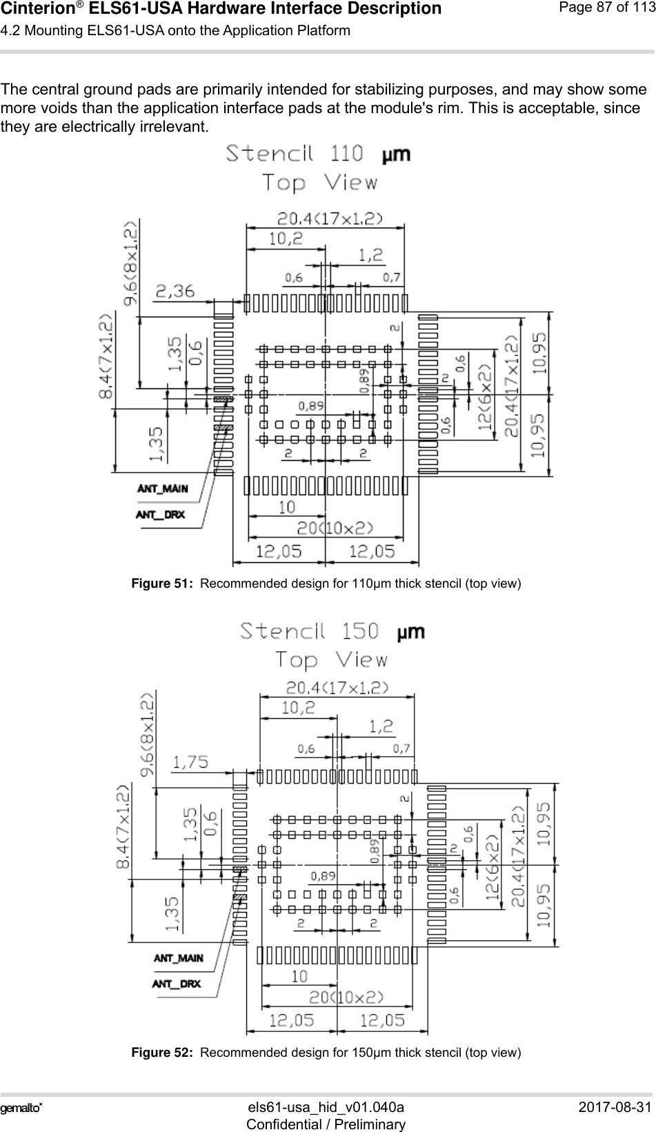
![Cinterion® ELS61-USA Hardware Interface Description4.2 Mounting ELS61-USA onto the Application Platform98els61-usa_hid_v01.040a 2017-08-31Confidential / PreliminaryPage 86 of 1134.2 Mounting ELS61-USA onto the Application PlatformThis section describes how to mount ELS61-USA onto the PCBs, including land pattern and stencil design, board-level characterization, soldering conditions, durability and mechanical handling. For more information on issues related to SMT module integration see also [3].Note: To avoid short circuits between signal tracks on an external application's PCB and vari-ous markings at the bottom side of the module, it is recommended not to route the signal tracks on the top layer of an external PCB directly under the module, or at least to ensure that signal track routes are sufficiently covered with solder resist.4.2.1 SMT PCB Assembly4.2.1.1 Land Pattern and StencilThe land pattern and stencil design as shown below is based on Gemalto characterizations for lead-free solder paste on a four-layer test PCB and a respectively 110 µm and 150 µm thick stencil. The land pattern given in Figure 50 reflects the module‘s pad layout, including signal pads and ground pads (for pad assignment see Section 2.1.1).Figure 50: Land pattern (top view)The stencil design illustrated in Figure 51 and Figure 52 is recommended by Gemalto M2M as a result of extensive tests with Gemalto M2M Daisy Chain modules.](https://usermanual.wiki/THALES-DIS-AlS-Deutschland/ELS61-USA/User-Guide-3601224-Page-86.png)
![Cinterion® ELS61-USA Hardware Interface Description4.2 Mounting ELS61-USA onto the Application Platform98els61-usa_hid_v01.040a 2017-08-31Confidential / PreliminaryPage 88 of 1134.2.1.2 Board Level CharacterizationBoard level characterization issues should also be taken into account if devising an SMT pro-cess.Characterization tests should attempt to optimize the SMT process with regard to board level reliability. This can be done by performing the following physical tests on sample boards: Peel test, bend test, tensile pull test, drop shock test and temperature cycling. Sample surface mount checks are described in [3].It is recommended to characterize land patterns before an actual PCB production, taking indi-vidual processes, materials, equipment, stencil design, and reflow profile into account. For land and stencil pattern design recommendations see also Section 4.2.1.1. Optimizing the solder stencil pattern design and print process is necessary to ensure print uniformity, to decrease sol-der voids, and to increase board level reliability.Daisy chain modules for SMT characterization are available on request. For details refer to [3].Generally, solder paste manufacturer recommendations for screen printing process parame-ters and reflow profile conditions should be followed. Maximum ratings are described in Section 4.2.3.4.2.2 Moisture Sensitivity LevelELS61-USA comprises components that are susceptible to damage induced by absorbed moisture.Gemalto M2M’s ELS61-USA module complies with the latest revision of the IPC/JEDEC J-STD-020 Standard for moisture sensitive surface mount devices and is classified as MSL 4.For additional moisture sensitivity level (MSL) related information see Section 4.2.4 and Sec-tion 4.3.2.](https://usermanual.wiki/THALES-DIS-AlS-Deutschland/ELS61-USA/User-Guide-3601224-Page-88.png)
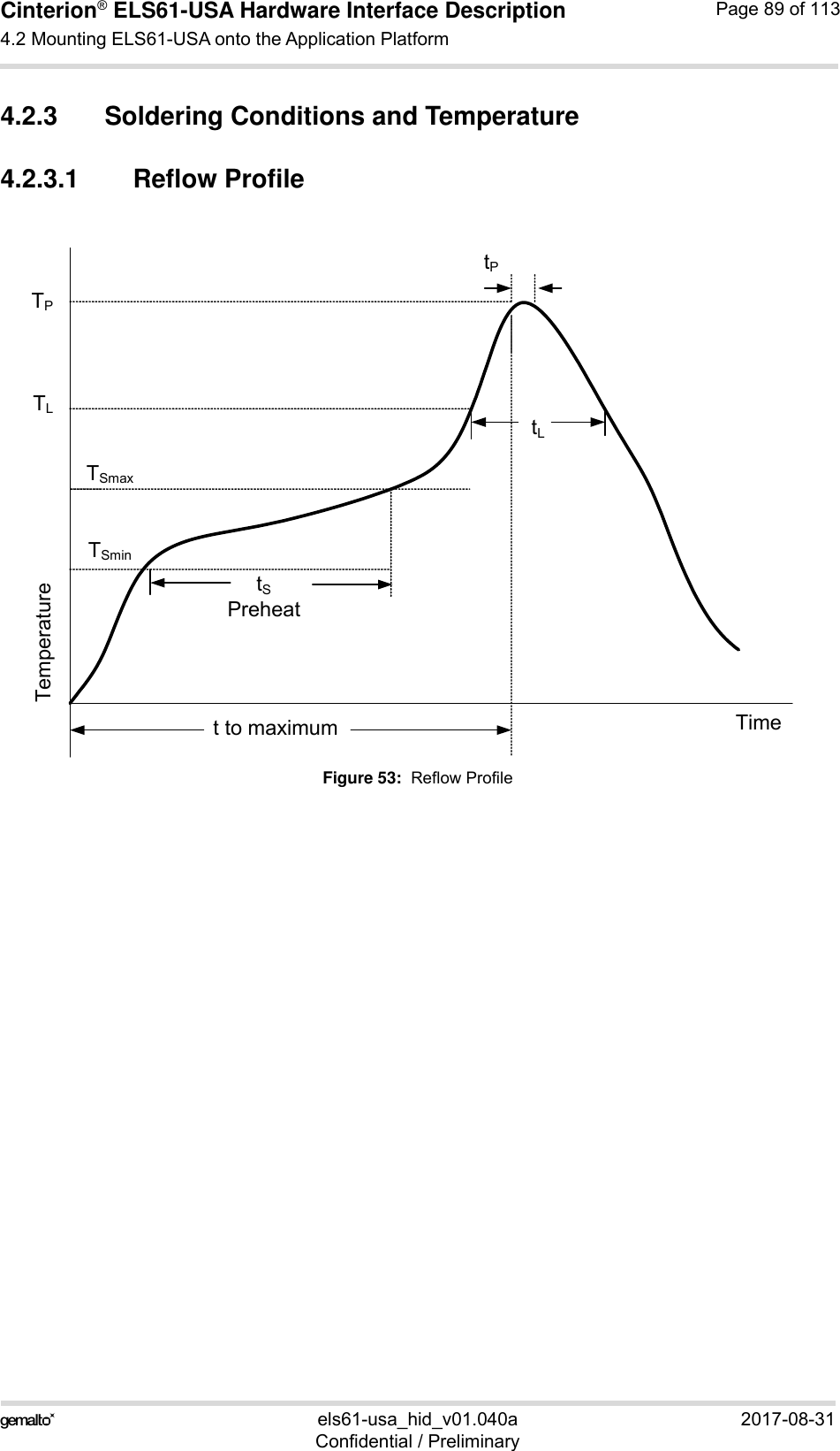
![Cinterion® ELS61-USA Hardware Interface Description4.2 Mounting ELS61-USA onto the Application Platform98els61-usa_hid_v01.040a 2017-08-31Confidential / PreliminaryPage 90 of 1134.2.3.2 Maximum Temperature and DurationThe following limits are recommended for the SMT board-level soldering process to attach the module:• A maximum module temperature of 245°C. This specifies the temperature as measured atthe module’s top side.• A maximum duration of 30 seconds at this temperature.Please note that while the solder paste manufacturers' recommendations for best temperature and duration for solder reflow should generally be followed, the limits listed above must not be exceeded.ELS61-USA is specified for one soldering cycle only. Once ELS61-USA is removed from the application, the module will very likely be destroyed and cannot be soldered onto another ap-plication.Table 21: Reflow temperature ratings1 1. Please note that the reflow profile features and ratings listed above are based on the joint industry standard IPC/JEDEC J-STD-020D.1, and are as such meant as a general guideline. For more information on reflow profiles and their optimization please refer to [3].Profile Feature Pb-Free AssemblyPreheat & SoakTemperature Minimum (TSmin)Temperature Maximum (TSmax)Time (tSmin to tSmax) (tS)150°C200°C60-120 secondsAverage ramp up rate (TL to TP) 3K/second max. 22. Temperatures measured on shielding at each corner. See also [3].Liquidous temperature (TL)Time at liquidous (tL)217°C50-90 secondsPeak package body temperature (TP)245°C +0/-5°CTime (tP) within 5 °C of the peak package body tem-perature (TP)30 seconds max.Average ramp-down rate 3 K/second max. 2Time 25°C to maximum temperature 8 minutes max.1423ModuleTemperature sensors (1-4)](https://usermanual.wiki/THALES-DIS-AlS-Deutschland/ELS61-USA/User-Guide-3601224-Page-90.png)
![Cinterion® ELS61-USA Hardware Interface Description4.3 Packaging98els61-usa_hid_v01.040a 2017-08-31Confidential / PreliminaryPage 98 of 1134.3.3 TraysIf small module quantities are required, e.g., for test and evaluation purposes, ELS61-USA may be distributed in trays (for dimensions see Figure 60). The small quantity trays are an alterna-tive to the single-feed tape carriers normally used. However, the trays are not designed for ma-chine processing. They contain modules to be (hand) soldered onto an external application (for information on hand soldering see [3]).Trays are packed and shipped in the same way as tape carriers, including a moisture barrier bag with desiccant and humidity indicator card as well as a transportation box (see also Section 4.3.2).Figure 60: Tray dimensions](https://usermanual.wiki/THALES-DIS-AlS-Deutschland/ELS61-USA/User-Guide-3601224-Page-98.png)
![Cinterion® ELS61-USA Hardware Interface Description6 Document Information110els61-usa_hid_v01.040a 2017-08-31Confidential / PreliminaryPage 106 of 1136 Document Information6.1 Revision HistoryPreceding document: "Cinterion® ELS61-USA Hardware Interface Description" Version 01.040New document: "Cinterion® ELS61-USA Hardware Interface Description" Version 01.040aNew document: "Cinterion® ELS61-USA Hardware Interface Description" Version 01.0406.2 Related Documents[1] ELS61-USA AT Command Set[2] ELS61-USA Release Note[3] Application Note 48: SMT Module Integration[4] Application Note 40: Thermal Solutions[5] Universal Serial Bus Specification Revision 2.0, April 27, 20006.3 Terms and AbbreviationsChapter What is new3.2.1.3 Updated chapter’s description.3.2.1.2 Updated Figure 37 regarding EMERG_RST.3.2.2.2 Updated Figure 40 regarding EMERG_RST.Chapter What is new-- Initial document setup.Abbreviation DescriptionADC Analog-to-digital converterAGC Automatic Gain ControlANSI American National Standards InstituteARFCN Absolute Radio Frequency Channel NumberARP Antenna Reference PointASC0/ASC1 Asynchronous Controller. Abbreviations used for first and second serial interface of ELS61-USAB Thermistor ConstantBER Bit Error RateBIP Bearer Independent ProtocolBTS Base Transceiver StationCB or CBM Cell Broadcast Message](https://usermanual.wiki/THALES-DIS-AlS-Deutschland/ELS61-USA/User-Guide-3601224-Page-106.png)