THALES DIS AlS Deutschland PH8-P GSM/GPRS/UMTS/HSPA Module User Manual hio
Gemalto M2M GmbH GSM/GPRS/UMTS/HSPA Module hio
Contents
- 1. User Manual
- 2. user manual
user manual

PH8/PH8-P
Version: 02.000
DocId: PH8_PH8-P_HD_v02.000
Hardware Interface Overview

GENERAL NOTE
THE USE OF THE PRODUCT INCLUDING THE SOFTWARE AND DOCUMENTATION (THE "PROD-
UCT") IS SUBJECT TO THE RELEASE NOTE PROVIDED TOGETHER WITH PRODUCT. IN ANY
EVENT THE PROVISIONS OF THE RELEASE NOTE SHALL PREVAIL. THIS DOCUMENT CON-
TAINS INFORMATION ON CINTERION PRODUCTS. THE SPECIFICATIONS IN THIS DOCUMENT
ARE SUBJECT TO CHANGE AT CINTERION'S DISCRETION. CINTERION WIRELESS MODULES
GMBH GRANTS A NON-EXCLUSIVE RIGHT TO USE THE PRODUCT. THE RECIPIENT SHALL NOT
TRANSFER, COPY, MODIFY, TRANSLATE, REVERSE ENGINEER, CREATE DERIVATIVE WORKS;
DISASSEMBLE OR DECOMPILE THE PRODUCT OR OTHERWISE USE THE PRODUCT EXCEPT
AS SPECIFICALLY AUTHORIZED. THE PRODUCT AND THIS DOCUMENT ARE PROVIDED ON AN
"AS IS" BASIS ONLY AND MAY CONTAIN DEFICIENCIES OR INADEQUACIES. TO THE MAXIMUM
EXTENT PERMITTED BY APPLICABLE LAW, CINTERION WIRELESS MODULES GMBH DIS-
CLAIMS ALL WARRANTIES AND LIABILITIES. THE RECIPIENT UNDERTAKES FOR AN UNLIMITED
PERIOD OF TIME TO OBSERVE SECRECY REGARDING ANY INFORMATION AND DATA PRO-
VIDED TO HIM IN THE CONTEXT OF THE DELIVERY OF THE PRODUCT. THIS GENERAL NOTE
SHALL BE GOVERNED AND CONSTRUED ACCORDING TO GERMAN LAW.
Copyright
Transmittal, reproduction, dissemination and/or editing of this document as well as utilization of its con-
tents and communication thereof to others without express authorization are prohibited. Offenders will
be held liable for payment of damages. All rights created by patent grant or registration of a utility model
or design patent are reserved.
Copyright © 2011, Cinterion Wireless Modules GmbH
Trademark Notice
Microsoft and Windows are either registered trademarks or trademarks of Microsoft Corporation in the
United States and/or other countries. All other registered trademarks or trademarks mentioned in this
document are property of their respective owners.
PH8_PH8-P_HD_v02.000 Page 2 of 46 2011-10-21
Confidential / Released
PH8/PH8-P Hardware Interface Overview
2
Document Name: PH8/PH8-P Hardware Interface Overview
Version: 02.000
Date: 2011-10-21
DocId: PH8_PH8-P_HD_v02.000
Status Confidential / Released

PH8/PH8-P Hardware Interface Overview
Contents
46
PH8_PH8-P_HD_v02.000 Page 3 of 46 2011-10-21
Confidential / Released
Contents
1 Introduction ................................................................................................................. 6
1.1 Related Documents ........................................................................................... 6
1.2 Terms and Abbreviations ................................................................................... 6
1.3 Regulatory and Type Approval Information ....................................................... 9
1.3.1 Directives and Standards...................................................................... 9
1.3.2 SAR requirements specific to portable mobiles .................................. 12
1.3.3 SELV Requirements ........................................................................... 13
1.3.4 Safety Precautions.............................................................................. 13
2 Product Concept ....................................................................................................... 15
2.1 Key Features at a Glance ................................................................................ 15
2.2 PH8/PH8-P System Overview ......................................................................... 18
3 Application Interface................................................................................................. 19
3.1 Operating Modes ............................................................................................. 20
3.2 Power Supply................................................................................................... 21
3.3 USB Interface................................................................................................... 22
3.4 Serial Interface ASC0 ...................................................................................... 23
3.5 UICC/SIM/USIM Interface................................................................................ 25
3.6 Analog Audio Interface..................................................................................... 27
3.7 Digital Audio Interface...................................................................................... 27
4 GPS Receiver............................................................................................................. 28
5 Antenna Interfaces.................................................................................................... 29
5.1 GSM/UMTS Antenna Interface ........................................................................ 29
5.1.1 Antenna Installation ............................................................................ 29
5.1.2 Antenna Connector ............................................................................. 30
5.2 GPS Antenna Interface .................................................................................... 34
6 Mechanics.................................................................................................................. 35
6.1 Mechanical Dimensions of PH8/PH8-P ........................................................... 35
6.2 Mounting PH8/PH8-P to the Application Platform............................................ 37
6.3 Board-to-Board Application Connector ............................................................ 37
7 Sample Application................................................................................................... 41
8 Reference Approval .................................................................................................. 43
8.1 Reference Equipment for Type Approval......................................................... 43
8.2 Compliance with FCC and IC Rules and Regulations ..................................... 44
9 Appendix.................................................................................................................... 45
9.1 List of Parts and Accessories........................................................................... 45

PH8/PH8-P Hardware Interface Overview
Tab le s
46
PH8_PH8-P_HD_v02.000 Page 4 of 46 2011-10-21
Confidential / Released
Tables
Table 1: Directives ......................................................................................................... 9
Table 2: Standards of North American type approval .................................................... 9
Table 3: Standards of European type approval.............................................................. 9
Table 4: Requirements of quality ................................................................................. 10
Table 5: Standards of the Ministry of Information Industry of the
People’s Republic of China............................................................................ 10
Table 6: Toxic or hazardous substances or elements with defined concentration
limits............................................................................................................... 11
Table 7: Overview of operating modes ........................................................................ 20
Table 8: DCE-DTE wiring of ASC0 .............................................................................. 24
Table 9: Signals of the SIM interface (board-to-board connector) ............................... 25
Table 10: Return loss in the active band........................................................................ 29
Table 11: Product specifications of PH8/PH8-P antenna connectors............................ 30
Table 12: Material and finish of PH8/PH8-P antenna connectors and recommended
plugs .............................................................................................................. 31
Table 13: Ordering information for Hirose U.FL Series.................................................. 33
Table 14: Technical specifications of Molex board-to-board connector......................... 38
Table 15: List of parts and accessories.......................................................................... 45
Table 16: Molex sales contacts (subject to change) ...................................................... 46
Table 17: Hirose sales contacts (subject to change) ..................................................... 46

PH8/PH8-P Hardware Interface Overview
Figures
46
PH8_PH8-P_HD_v02.000 Page 5 of 46 2011-10-21
Confidential / Released
Figures
Figure 1: PH8/PH8-P system overview......................................................................... 18
Figure 2: USB circuit ..................................................................................................... 22
Figure 3: Serial interface ASC0..................................................................................... 23
Figure 4: UICC/SIM/USIM interface .............................................................................. 26
Figure 5: Mechanical dimensions of PH8/PH8-P antenna connectors.......................... 30
Figure 6: U.FL-R-SMT connector with U.FL-LP-040 plug ............................................. 31
Figure 7: U.FL-R-SMT connector with U.FL-LP-066 plug ............................................. 31
Figure 8: Specifications of U.FL-LP-(V)-040(01) plug ................................................... 32
Figure 9: PH8/PH8-P – top and bottom view ................................................................ 35
Figure 10: Dimensions of PH8/PH8-P (all dimensions in mm)........................................ 36
Figure 11: Mating board-to-board connector 53748-0808 on application ....................... 38
Figure 12: Molex board-to-board connector 52991-0808 on PH8/PH8-P ....................... 39
Figure 13: Mating board-to-board connector 53748-0808 on application ....................... 40
Figure 14: PH8/PH8-P sample application...................................................................... 42
Figure 15: Reference equipment for type approval......................................................... 43

PH8/PH8-P Hardware Interface Overview
1 Introduction
14
PH8_PH8-P_HD_v02.000 Page 6 of 46 2011-10-21
Confidential / Released
1 Introduction
The document1 describes the hardware of the PH8/PH8-P module, designed to connect to a
cellular device application and the air interface. It helps you quickly retrieve interface specifica-
tions, electrical and mechanical details and information on the requirements to be considered
for integrating further components.
1.1 Related Documents
[1] PH8/PH8-P AT Command Set
[2] PH8/PH8-P Release Notes
[3] DSB75 Support Box - Evaluation Kit for Cinterion Wireless Modules
1.2 Terms and Abbreviations
1. The document is effective only if listed in the appropriate Release Notes as part of the technical
documentation delivered with your Cinterion Wireless Modules product.
Abbreviation Description
AGPS Assisted GPS
ANSI American National Standards Institute
AMR Adaptive Multirate
ARP Antenna Reference Point
B2B Board-to-board connector
BB Baseband
BEP Bit Error Probability
BTS Base Transceiver Station
CB or CBM Cell Broadcast Message
CE Conformité Européene (European Conformity)
CS Coding Scheme
CS Circuit Switched
CSD Circuit Switched Data
CTM Cellular Text Modem
DAC Digital-to-Analog Converter
DCS Digital Cellular System
DL Download
DRX Discontinuous Reception
DSB Development Support Board

PH8/PH8-P Hardware Interface Overview
1.2 Terms and Abbreviations
14
PH8_PH8-P_HD_v02.000 Page 7 of 46 2011-10-21
Confidential / Released
DSP Digital Signal Processor
DTMF Dual Tone Multi Frequency
DTX Discontinuous Transmission
EDGE Enhanced Data rates for GSM Evolution
EFR Enhanced Full Rate
EGSM Extended GSM
EMC Electromagnetic Compatibility
ERP Effective Radiated Power
ESD Electrostatic Discharge
ETS European Telecommunication Standard
ETSI European Telecommunications Standards Institute
FCC Federal Communications Commission (U.S.)
FDD Frequency Division Duplex
FDMA Frequency Division Multiple Access
FR Full Rate
GPRS General Packet Radio Service
GPS Global Positioning System
GSM Global Standard for Mobile Communications
HiZ High Impedance
HSDPA High Speed Downlink Packet Access
HR Half Rate
I/O Input/Output
IF Intermediate Frequency
IMEI International Mobile Equipment Identity
ISO International Standards Organization
ITU International Telecommunications Union
kbps kbits per second
LED Light Emitting Diode
Mbps Mbits per second
MCS Modulation and Coding Scheme
MO Mobile Originated
MS Mobile Station, also referred to as TE
MT Mobile Terminated
NMEA National Marine Electronics Association
NTC Negative Temperature Coefficient
PBCCH Packet Switched Broadcast Control Channel
Abbreviation Description

PH8/PH8-P Hardware Interface Overview
1.2 Terms and Abbreviations
14
PH8_PH8-P_HD_v02.000 Page 8 of 46 2011-10-21
Confidential / Released
PCB Printed Circuit Board
PCL Power Control Level
PCM Pulse Code Modulation
PCS Personal Communication System, also referred to as GSM 1900
PDU Protocol Data Unit
PS Packet Switched
PSK Phase Shift Keying
QAM Quadrature Amplitude Modulation
R&TTE Radio and Telecommunication Terminal Equipment
RF Radio Frequency
ROPR Radio Output Power Reduction
RTC Real Time Clock
Rx Receive Direction
SAR Specific Absorption Rate
SELV Safety Extra Low Voltage
SIM Subscriber Identification Module
SLIC Subscriber Line Interface Circuit
SMPL Sudden Momentary Power Loss
SMS Short Message Service
SNR Signal-to-Noise Ratio
SRAM Static Random Access Memory
SRB Signalling Radio Bearer
SUPL Secure User Plane Location
TDMA Time Division Multiple Access
TE Terminal Equipment
TPC Transmit Power Control
TS Technical Specification
TTFF Time To First Fix
Tx Transmit Direction
UL Upload
UMTS Universal Mobile Telecommunications System
URC Unsolicited Result Code
USB Universal Serial Bus
UICC USIM Integrated Circuit Card
USIM UMTS Subscriber Identification Module
WCDMA Wideband Code Division Multiple Access
Abbreviation Description
PH8/PH8-P Hardware Interface Overview
1.3 Regulatory and Type Approval Information
14
PH8_PH8-P_HD_v02.000 Page 9 of 46 2011-10-21
Confidential / Released
1.3 Regulatory and Type Approval Information
1.3.1 Directives and Standards
PH8/PH8-P has been designed to comply with the directives and standards listed below.
It is the responsibility of the application manufacturer to ensure compliance of the final product
with all provisions of the applicable directives and standards as well as with the technical spec-
ifications provided in the "PH8/PH8-P Hardware Interface Description".1
1. Manufacturers of applications which can be used in the US shall ensure that their applications have a
PTCRB approval. For this purpose they can refer to the PTCRB approval of the respective module.
Table 1: Directives
99/05/EC Directive of the European Parliament and of the council of 9 March 1999 on
radio equipment and telecommunications terminal equipment and the
mutual recognition of their conformity (in short referred to as R&TTE Direc-
tive 1999/5/EC).
The product is labeled with the CE conformity mark
2002/95/EC Directive of the European Parliament and of the Council of
27 January 2003 on the restriction of the use of certain haz-
ardous substances in electrical and electronic equipment
(RoHS)
Table 2: Standards of North American type approval
CFR Title 47 Code of Federal Regulations, Part 22, Part 24 and Part 27; US Equipment
Authorization FCC
OET Bulletin 65
(Edition 97-01)
Evaluating Compliance with FCC Guidelines for Human Exposure to Radio-
frequency Electromagnetic Fields
UL 60 950-1 Product Safety Certification (Safety requirements)
NAPRD.03 V5.8 Overview of PCS Type certification review board Mobile Equipment Type
Certification and IMEI control
PCS Type Certification Review board (PTCRB)
RSS132, RSS133,
RSS139
Canadian Standard
Table 3: Standards of European type approval
3GPP TS 51.010-1 Digital cellular telecommunications system (Release 7); Mobile Station
(MS) conformance specification;
ETSI EN 301 511 V9.0.2 Global System for Mobile communications (GSM); Harmonized standard for
mobile stations in the GSM 900 and DCS 1800 bands covering essential
requirements under article 3.2 of the R&TTE directive (1999/5/EC)
GCF-CC V3.43.1 Global Certification Forum - Certification Criteria
ETSI EN 301 489-01
V1.8.1
Electromagnetic Compatibility and Radio spectrum Matters (ERM); Electro-
magnetic Compatibility (EMC) standard for radio equipment and services;
Part 1: Common Technical Requirements
PH8/PH8-P Hardware Interface Overview
1.3 Regulatory and Type Approval Information
14
PH8_PH8-P_HD_v02.000 Page 10 of 46 2011-10-21
Confidential / Released
ETSI EN 301 489-03
V1.4.1
Electromagnetic Compatibility and Radio spectrum Matters (ERM); Electro-
magnetic Compatibility (EMC) standard for radio equipment and services;
Part 3: Specific conditions for Short-Range Devices (SRD) operating on fre-
quencies between 9 kHz and 40 GHz
ETSI EN 301 489-07
V1.3.1
Electromagnetic Compatibility and Radio spectrum Matters (ERM); Electro-
magnetic Compatibility (EMC) standard for radio equipment and services;
Part 7: Specific conditions for mobile and portable radio and ancillary equip-
ment of digital cellular radio telecommunications systems (GSM and DCS)
ETSI EN 301 489-24
V1.4.1
Electromagnetic Compatibility and Radio spectrum Matters (ERM); Electro-
magnetic Compatibility (EMC) standard for radio equipment and services;
Part 24: Specific conditions for IMT-2000 CDMA Direct Spread (UTRA) for
Mobile and portable (UE) radio and ancillary equipment
EN 301 908-01 V3.2.1 Electromagnetic compatibility and Radio spectrum Matters (ERM); Base
Stations (BS) and User Equipment (UE) for IMT-2000 Third Generation cel-
lular networks; Part 1: Harmonized EN for IMT-2000, introduction and com-
mon requirements of article 3.2 of the R&TTE Directive
EN 301 908-02 V3.2.1 Electromagnetic compatibility and Radio spectrum Matters (ERM); Base
Stations (BS) and User Equipment (UE) for IMT-2000 Third Generation cel-
lular networks; Part 2: Harmonized EN for IMT-2000, CDMA Direct Spread
(UTRA FDD) (UE) covering essential requirements of article 3.2 of the
R&TTE Directive
EN 300 440-02 V1.3.1 Electromagnetic compatibility and Radio spectrum Matters (ERM); Short
range devices; Radio equipment to be used in the 1 GHz to 40 GHz fre-
quency range; Part 2: Harmonized EN covering essential requirements of
article 3.2 of the R&TTE Directive
EN 62311:2008 Assessment of electronic and electrical equipment related to human expo-
sure restrictions for electromagnetic fields (0 Hz - 300 GHz)
IEC/EN 60950-1:2006 Safety of information technology equipment
Table 4: Requirements of quality
IEC 60068 Environmental testing
DIN EN 60529 IP codes
Table 5: Standards of the Ministry of Information Industry of the People’s Republic of China
SJ/T 11363-2006 “Requirements for Concentration Limits for Certain Hazardous Substances
in Electronic Information Products” (2006-06).
SJ/T 11364-2006 “Marking for Control of Pollution Caused by Electronic
Information Products” (2006-06).
According to the “Chinese Administration on the Control of
Pollution caused by Electronic Information Products”
(ACPEIP) the EPUP, i.e., Environmental Protection Use
Period, of this product is 20 years as per the symbol
shown here, unless otherwise marked. The EPUP is valid only as long as
the product is operated within the operating limits described in the Cinterion
Hardware Interface Description.
Please see Table 6 for an overview of toxic or hazardous substances or ele-
ments that might be contained in product parts in concentrations above the
limits defined by SJ/T 11363-2006.
Table 3: Standards of European type approval

PH8/PH8-P Hardware Interface Overview
1.3 Regulatory and Type Approval Information
14
PH8_PH8-P_HD_v02.000 Page 12 of 46 2011-10-21
Confidential / Released
1.3.2 SAR requirements specific to portable mobiles
Mobile phones, PDAs or other portable transmitters and receivers incorporating a GSM module
must be in accordance with the guidelines for human exposure to radio frequency energy. This
requires the Specific Absorption Rate (SAR) of portable PH8/PH8-P based applications to be
evaluated and approved for compliance with national and/or international regulations.
Since the SAR value varies significantly with the individual product design manufacturers are
advised to submit their product for approval if designed for portable use. For European and US-
markets the relevant directives are mentioned below. It is the responsibility of the manufacturer
of the final product to verify whether or not further standards, recommendations or directives
are in force outside these areas.
Products intended for sale on US markets
ES 59005/ANSI C95.1 Considerations for evaluation of human exposure to electromagnetic
fields (EMFs) from mobile telecommunication equipment (MTE) in the
frequency range 30MHz - 6GHz
Products intended for sale on European markets
EN 50360 Product standard to demonstrate the compliance of mobile phones with
the basic restrictions related to human exposure to electromagnetic
fields (300MHz - 3GHz)
IMPORTANT:
Manufacturers of portable applications based on PH8/PH8-P modules are required to have
their final product certified and apply for their own FCC Grant and Industry Canada Certificate
related to the specific portable mobile.
PH8/PH8-P Hardware Interface Overview
1.3 Regulatory and Type Approval Information
14
PH8_PH8-P_HD_v02.000 Page 13 of 46 2011-10-21
Confidential / Released
1.3.3 SELV Requirements
The power supply connected to the PH8/PH8-P module shall be in compliance with the SELV
requirements defined in EN 60950-1.
1.3.4 Safety Precautions
The following safety precautions must be observed during all phases of the operation, usage,
service or repair of any cellular terminal or mobile incorporating PH8/PH8-P. Manufacturers of
the cellular terminal are advised to convey the following safety information to users and oper-
ating personnel and to incorporate these guidelines into all manuals supplied with the product.
Failure to comply with these precautions violates safety standards of design, manufacture and
intended use of the product. Cinterion Wireless Modules assumes no liability for customer’s
failure to comply with these precautions.
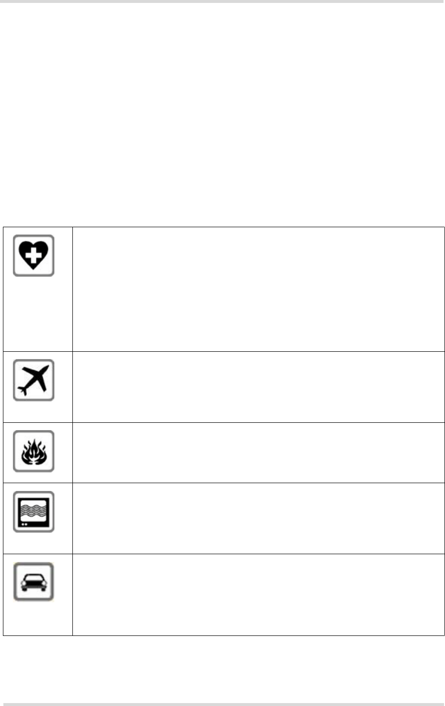
When in a hospital or other health care facility, observe the restrictions on the use of
mobiles. Switch the cellular terminal or mobile off, if instructed to do so by the guide-
lines posted in sensitive areas. Medical equipment may be sensitive to RF energy.
The operation of cardiac pacemakers, other implanted medical equipment and hearing
aids can be affected by interference from cellular terminals or mobiles placed close to
the device. If in doubt about potential danger, contact the physician or the manufac-
turer of the device to verify that the equipment is properly shielded. Pacemaker
patients are advised to keep their hand-held mobile away from the pacemaker, while
it is on.
Switch off the cellular terminal or mobile before boarding an aircraft. Make sure it can-
not be switched on inadvertently. The operation of wireless appliances in an aircraft is
forbidden to prevent interference with communications systems. Failure to observe
these instructions may lead to the suspension or denial of cellular services to the
offender, legal action, or both.
Do not operate the cellular terminal or mobile in the presence of flammable gases or
fumes. Switch off the cellular terminal when you are near petrol stations, fuel depots,
chemical plants or where blasting operations are in progress. Operation of any electri-
cal equipment in potentially explosive atmospheres can constitute a safety hazard.
Your cellular terminal or mobile receives and transmits radio frequency energy while
switched on. Remember that interference can occur if it is used close to TV sets,
radios, computers or inadequately shielded equipment. Follow any special regulations
and always switch off the cellular terminal or mobile wherever forbidden, or when you
suspect that it may cause interference or danger.
Road safety comes first! Do not use a hand-held cellular terminal or mobile when driv-
ing a vehicle, unless it is securely mounted in a holder for speakerphone operation.
Before making a call with a hand-held terminal or mobile, park the vehicle.
Speakerphones must be installed by qualified personnel. Faulty installation or opera-
tion can constitute a safety hazard.

PH8/PH8-P Hardware Interface Overview
1.3 Regulatory and Type Approval Information
14
PH8_PH8-P_HD_v02.000 Page 14 of 46 2011-10-21
Confidential / Released
IMPORTANT!
Cellular terminals or mobiles operate using radio signals and cellular networks.
Because of this, connection cannot be guaranteed at all times under all conditions.
Therefore, you should never rely solely upon any wireless device for essential com-
munications, for example emergency calls.
Remember, in order to make or receive calls, the cellular terminal or mobile must be
switched on and in a service area with adequate cellular signal strength.
Some networks do not allow for emergency calls if certain network services or phone
features are in use (e.g. lock functions, fixed dialing etc.). You may need to deactivate
those features before you can make an emergency call.
Some networks require that a valid SIM card be properly inserted in the cellular termi-
nal or mobile.
Bear in mind that exposure to excessive levels of noise can cause physical damage
to users! With regard to acoustic shock, the cellular application must be designed to
avoid unintentional increase of amplification, e.g. for a highly sensitive earpiece. A pro-
tection circuit should be implemented in the cellular application.

PH8/PH8-P Hardware Interface Overview
2 Product Concept
18
PH8_PH8-P_HD_v02.000 Page 15 of 46 2011-10-21
Confidential / Released
2 Product Concept
2.1 Key Features at a Glance
Feature Implementation
General
Frequency bands GSM/GPRS/EDGE: Quad band, 850/900/1800/1900MHz
UMTS/HSPA+:
PH8: Five band, 800/850/AWS1/1900/2100MHz
PH8-P: Five band, 800/850/9002/1900/2100MHz
GSM class Small MS
Output power (according to
Release 99)
Class 4 (+33dBm ±2dB) for EGSM850
Class 4 (+33dBm ±2dB) for EGSM900
Class 1 (+30dBm ±2dB) for GSM1800
Class 1 (+30dBm ±2dB) for GSM1900
Class E2 (+27dBm ± 3dB) for GSM 850 8-PSK
Class E2 (+27dBm ± 3dB) for GSM 900 8-PSK
Class E2 (+26dBm +3 /-4dB) for GSM 1800 8-PSK
Class E2 (+26dBm +3 /-4dB) for GSM 1900 8-PSK
Class 3 (+24dBm +1/-3dB) for UMTS 2100, WCDMA FDD BdI
Class 3 (+24dBm +1/-3dB) for UMTS 1900,WCDMA FDD BdII
Class 3 (+24dBm +1/-3dB) for UMTS AWS, WCDMA FDD BdIV1
Class 3 (+24dBm +1/-3dB) for UMTS 900, WCDMA FDD BdVIII2
Class 3 (+24dBm +1/-3dB) for UMTS 850, WCDMA FDD BdV
Class 3 (+24dBm +1/-3dB) for UMTS 800, WCDMA FDD BdVI
Power supply 3.3V < VBATT+ < 4.2V
Operating temperature
(board temperature)
Normal operation: -30°C to +85°C
Restricted operation: -40°C to +95°C
Physical Dimensions: 33.9mm x 50mm x 3.1mm
Weight: approx. 9.5g
RoHS All hardware components fully compliant with EU RoHS Directive
HSPA features
3GPP Release 6, 7 DL 14.4Mbps, UL 5.7Mbps
UE CAT. 1-12 supported
Compressed mode (CM) supported according to 3GPP TS25.212
UMTS features
3GPP Release 4 PS data rate – 384 kbps DL / 384 kbps UL
CS data rate – 64 kbps DL / 64 kbps UL

PH8/PH8-P Hardware Interface Overview
2.1 Key Features at a Glance
18
PH8_PH8-P_HD_v02.000 Page 16 of 46 2011-10-21
Confidential / Released
GSM / GPRS / EGPRS features
Data transfer GPRS:
• Multislot Class 12
• Full PBCCH support
• Mobile Station Class B
• Coding Scheme 1 – 4
EGPRS:
• Multislot Class 12
• EDGE E2 power class for 8 PSK
• Downlink coding schemes – CS 1-4, MCS 1-9
• Uplink coding schemes – CS 1-4, MCS 1-9
• SRB loopback and test mode B
• 8-bit, 11-bit RACH
• PBCCH support
• 1 phase/2 phase access procedures
• Link adaptation and IR
• NACC, extended UL TBF
• Mobile Station Class B
CSD:
• V.110, RLP, non-transparent
• 14.4kbps
• USSD
SMS Point-to-point MT and MO
Cell broadcast
Text and PDU mode
GPS Features
Protocol NMEA
Modes Standalone GPS
Assisted GPS
- Control plane - E911
- User plane - gpsOneXTRA™
General Power saving modes
Power supply for active GPS antenna supported
Software
AT commands Hayes, 3GPP TS 27.007 and 27.005, and proprietary Cinterion Wireless
Modules commands
SIM Application Toolkit SAT Release 99
Audio Audio speech codecs
GSM: AMR, EFR, FR, HR
3GPP: AMR
Speakerphone operation, echo cancellation, noise suppression, 9 ringing
tones, TTY support
Firmware update Generic update from host application over ASC0 or USB
Interfaces
Module interface 80-pin board-to-board connector
Antenna 50Ohms. Main GSM/UMTS antenna, UMTS diversity antenna, GPS
antenna (active/passive)
Feature Implementation

PH8/PH8-P Hardware Interface Overview
2.1 Key Features at a Glance
18
PH8_PH8-P_HD_v02.000 Page 17 of 46 2011-10-21
Confidential / Released
USB USB 2.0 High Speed (480Mbit/s) device interface, Full Speed (12Mbit/s)
compliant
Serial interface ASC0:
• 8-wire modem interface with status and control lines, unbalanced,
asynchronous
• Adjustable baud rates from 9,600bps up to 921,600bps
• Supports RTS0/CTS0 hardware flow control
• Multiplex ability according to GSM 07.10 Multiplexer Protocol
UICC interface Supported chip cards: UICC/SIM/USIM 3V, 1.8V
Status Signal line to indicate network connectivity state
Audio 1 analog interface with microphone feeding
1 digital interface: PCM or I2S
Power on/off, Reset
Power on/off Switch-on by hardware signal IGT
Switch-off by AT command (AT^SMSO)
Automatic switch-off in case of critical temperature or voltage conditions
Reset Orderly shutdown and reset by AT command
Emergency-off Emergency-off by hardware signal EMERG_OFF if IGT is not active
Special Features
Phonebook SIM and phone
TTY/CTM support Integrated CTM modem
Antenna SAIC (Single Antenna Interference Cancellation) / DARP (Downlink
Advanced Receiver Performance)
Rx diversity (receiver type 3i - 16-QAM)3
Evaluation kit
DSB75 DSB75 Evaluation Board designed to test and type approve Cinterion
Wireless Modules and provide a sample configuration for application
engineering. A special adapter is required to connect the module to the
DSB75.
1. AWS UMTS/HSPA+ band IV supported by PH8 only.
2. 900MHz UMTS/HSPA+ band VIII supported by PH8-P only. Band VIII however, is not supported by
the UMTS Rx diversity antenna.
3. UMTS Rx diversity antenna does not support UMTS/HSPA+ band VIII.
Feature Implementation
PH8/PH8-P Hardware Interface Overview
2.2 PH8/PH8-P System Overview
18
PH8_PH8-P_HD_v02.000 Page 18 of 46 2011-10-21
Confidential / Released
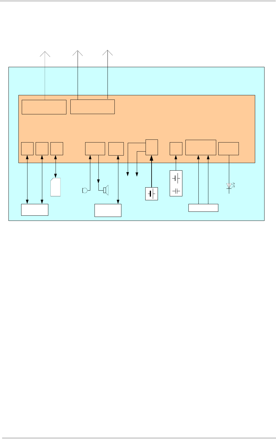
2.2 PH8/PH8-P System Overview
Figure 1: PH8/PH8-P system overview
USB Serial
ASC0 UICC Analog
audio
Power
supply RTC IGT,
Emergency Off
Net state/
status
SIM
card
Host
application
On/Off
Module
Application
or
GSM/UMTS
antenna
Power for application
(VEXT)
Power indication
(PWR_IND)
Modem interface
Digital
audio
PCM or I2S
codec
GSM/UMTS
GPS
GPS antenna
UMTS
diversity antenna

PH8/PH8-P Hardware Interface Overview
3 Application Interface
28
PH8_PH8-P_HD_v02.000 Page 19 of 46 2011-10-21
Confidential / Released
3 Application Interface
PH8/PH8-P is equipped with an 80-pin board-to-board connector that connects to the external
application. The host interface incorporates several sub-interfaces described in the following
sections:
• Operating modes - see Section 3.1
• Power supply - see Section 3.2
• Serial interface USB - see Section 3.3
• Serial interface ASC0 - Section 3.4
• UICC/SIM/USIM interface - see Section 3.5
• Analog audio interface - see Section 3.6
• Digital audio interface (PCM or I2S) - see Section 3.7

PH8/PH8-P Hardware Interface Overview
3.1 Operating Modes
28
PH8_PH8-P_HD_v02.000 Page 20 of 46 2011-10-21
Confidential / Released
3.1 Operating Modes
The table below briefly summarizes the various operating modes referred to in the following
chapters.
Table 7: Overview of operating modes
Mode Function
Normal
operation
GSM /
GPRS / UMTS /
HSPA SLEEP
Power saving set automatically when no call is in progress and the USB
connection is suspended by host or not present and no active commu-
nication via ASC0.
GSM /
GPRS / UMTS /
HSPA IDLE
Power saving disabled (see [1]: AT^SCFG "MEopMode/
PwrSave",<PwrSaveMode>) or an USB connection not suspended, but
no call in progress.
GSM TALK/
GSM DATA
Connection between two subscribers is in progress. Power consump-
tion depends on the GSM network coverage and several connection
settings (e.g. DTX off/on, FR/EFR/HR, hopping sequences and
antenna connection). The following applies when power is to be mea-
sured in TALK_GSM mode: DTX off, FR and no frequency hopping.
GPRS DATA GPRS data transfer in progress. Power consumption depends on net-
work settings (e.g. power control level), uplink / downlink data rates and
GPRS configuration (e.g. used multislot settings).
EGPRS DATA EGPRS data transfer in progress. Power consumption depends on net-
work settings (e.g. power control level), uplink / downlink data rates and
EGPRS configuration (e.g. used multislot settings).
UMTS TALK/
UMTS DATA
UMTS data transfer in progress. Power consumption depends on net-
work settings (e.g. TPC Pattern) and data transfer rate.
HSPA DATA HSPA data transfer in progress. Power consumption depends on net-
work settings (e.g. TPC Pattern) and data transfer rate.
Power
Down
Normal shutdown after sending the AT^SMSO command. Only a voltage regulator is active
for powering the RTC. Software is not active. Interfaces are not accessible. Operating volt-
age (connected to BATT+) remains applied.
Airplane
mode
Airplane mode shuts down the radio part of the module, causes the module to log off from
the GSM/GPRS network and disables all AT commands whose execution requires a radio
connection.
Airplane mode can be controlled by AT command (see [1]).

PH8/PH8-P Hardware Interface Overview
3.2 Power Supply
28
PH8_PH8-P_HD_v02.000 Page 21 of 46 2011-10-21
Confidential / Released
3.2 Power Supply
PH8/PH8-P needs to be connected to a power supply at the board-to-board connector - 5 lines
each BATT+ and GND.
The power supply of PH8/PH8-P has to be a single voltage source at BATT+. It must be able
to provide the peak current during the uplink transmission.
All key functions for supplying power to the device are handled by the power management IC.
It provides the following features:
• Stabilizes the supply voltages for the baseband using switching regulators and low drop lin-
ear voltage regulators.
• Switches the module's power voltages for the power-up and -down procedures.
• Delivers, across the VEXT line, a regulated voltage for an external application. This voltage
is not available in Power-down mode and can be reduced via AT command to save power.
• SIM switch to provide SIM power supply.
PH8/PH8-P Hardware Interface Overview
3.3 USB Interface
28
PH8_PH8-P_HD_v02.000 Page 22 of 46 2011-10-21
Confidential / Released
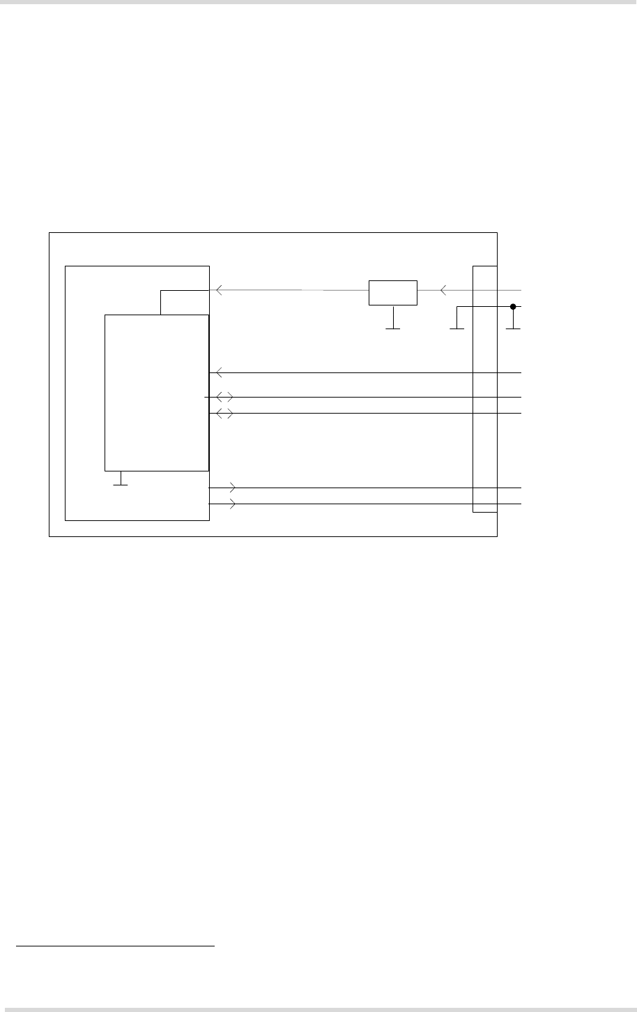
3.3 USB Interface
PH8/PH8-P supports a USB 2.0 High Speed (480Mbit/s) device interface that is Full Speed
(12Mbit/s) compliant. The USB interface is primarily intended for use as command and data
interface and for downloading firmware.
The USB host is responsible for supplying the VUSB_IN line. This line is for voltage detection
only. The USB part (driver and transceiver) is supplied by means of BATT+. This is because
PH8/PH8-P is designed as a self-powered device compliant with the “Universal Serial Bus
Specification Revision 2.0”1.
Figure 2: USB circuit
To properly connect the module's USB interface to the host a USB 2.0 compatible connector is
required. Furthermore, the USB modem driver distributed with PH8/PH8-P needs to be in-
stalled.
While the USB connection is active, the module will not change into SLEEP Mode. To enable
switching into SLEEP mode the USB host must bring its USB interface into Suspend state (see
“Universal Serial Bus Specification Revision 2.0“1 for a description of the Suspend state). On
incoming calls PH8/PH8-P will then generate a remote wake up request to resume the USB
connection (active low). If configured for SDPORT=6, i.e., if using a CDC ACM compatible USB
driver on the host system, a selective suspend on the USB host may not be supported and the
module may therefore not be able to change into SLEEP mode.
As an alternative to the regular USB remote wakeup mechanism it is possible to employ the
RING0 or WAKEUP line to wake up the host application. The benefit is that the RING0 or
WAKEUP lines can wake up the host application in case of incoming calls or other events sig-
nalized by URCs while the USB interface is suspended or shut down.
1. The specification is ready for download on http://www.usb.org/developers/docs/
VBUS
DP
DN
VREG (3V075)
BATT+
USB_DP2)
lin. reg.
GND
Module
Detection only VUSB_IN
USB part1)
RING0
Host wakeup
1) All serial and pull-up resistors for data lines are implemented.
USB_DN2)
2) If the USB interface is operated in High Speed mode (480MHz), it is recommended to take
special care routing the data lines USB_DP and USB_DN. Application layout should in this
case implement a differential impedance of 90Ohm for proper signal integrity.
WAKEUP
B2B
PH8/PH8-P Hardware Interface Overview
3.4 Serial Interface ASC0
28
PH8_PH8-P_HD_v02.000 Page 23 of 46 2011-10-21
Confidential / Released
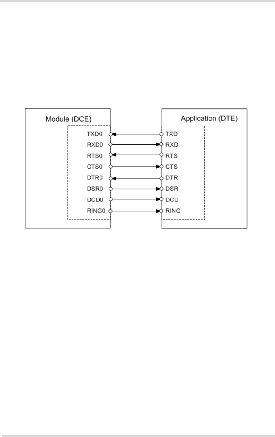
3.4 Serial Interface ASC0
PH8/PH8-P offers an 8-wire unbalanced, asynchronous modem interface ASC0 conforming to
ITU-T V.24 protocol DCE signalling. The electrical characteristics do not comply with ITU-T
V.28. The significant levels are 0V (for low data bit or active state) and 1.8V (for high data bit
or inactive state).
PH8/PH8-P is designed for use as a DCE. Based on the conventions for DCE-DTE connections
it communicates with the customer application (DTE) using the following signals:
• Port TXD @ application sends data to the module’s TXD0 signal line
• Port RXD @ application receives data from the module’s RXD0 signal line
Figure 3: Serial interface ASC0
Features:
• Includes the data lines TXD0 and RXD0, the status lines RTS0 and CTS0 and, in addition,
the modem control lines DTR0, DSR0, DCD0 and RING0.
• ASC0 is designed for controlling GSM/UMTS voice calls, transferring data and for control-
ling the module with AT commands.
• Full multiplexing capability allows the interface to be partitioned into virtual channels.
• The RING0 signal serves to indicate incoming calls and other types of URCs (Unsolicited
Result Code). It can also be used to send pulses to the host application, for example to
wake up the application from power saving state. See [1] for details on how to configure the
RING0 line by AT^SCFG.
• Configured for 8 data bits, no parity and 1 stop bit.
• ASC0 can be operated at fixed bit rates from 9600bps up to 921600bps.
• Supports RTS0/CTS0 hardware flow control.
• Wake up from SLEEP mode by RTS0 activation (high to low transition).
Note. If the ASC0 serial interface is the application’s only interface, it is suggested to connect
test points on the USB signal lines as a potential tracing possibility.

PH8/PH8-P Hardware Interface Overview
3.4 Serial Interface ASC0
28
PH8_PH8-P_HD_v02.000 Page 24 of 46 2011-10-21
Confidential / Released
Table 8: DCE-DTE wiring of ASC0
V.24 circuit DCE DTE
Line function Signal direction Line function Signal direction
103 TXD0 Input TXD Output
104 RXD0 Output RXD Input
105 RTS0 Input RTS Output
106 CTS0 Output CTS Input
108/2 DTR0 Input DTR Output
107 DSR0 Output DSR Input
109 DCD0 Output DCD Input
125 RING0 Output RING Input

PH8/PH8-P Hardware Interface Overview
3.5 UICC/SIM/USIM Interface
28
PH8_PH8-P_HD_v02.000 Page 25 of 46 2011-10-21
Confidential / Released
3.5 UICC/SIM/USIM Interface
PH8/PH8-P has an integrated UICC/SIM/USIM interface compatible with the 3GPP 31.102 and
ETSI 102 221. This is wired to the host interface in order to be connected to an external SIM
card holder. Six pins on the board-to-board connector are reserved for the SIM interface.
The UICC/SIM/USIM interface supports 3V and 1.8V SIM cards.
The CCIN signal serves to detect whether a tray (with SIM card) is present in the card holder.
Using the CCIN signal is mandatory for compliance with the GSM 11.11 recommendation if the
mechanical design of the host application allows the user to remove the SIM card during oper-
ation. To take advantage of this feature, an appropriate SIM card detect switch is required on
the card holder. For example, this is true for the model supplied by Molex, which has been test-
ed to operate with PH8/PH8-P and is part of the Cinterion reference equipment submitted for
type approval. See Chapter 9 for Molex ordering numbers.
Note: No guarantee can be given, nor any liability accepted, if loss of data is encountered after
removing the SIM card during operation. Also, no guarantee can be given for properly initializ-
ing any SIM card that the user inserts after having removed the SIM card during operation. In
this case, the application must restart PH8/PH8-P.
Table 9: Signals of the SIM interface (board-to-board connector)
Signal Description
CCGND Separate ground connection for SIM card to improve EMC.
Be sure to use this ground line for the SIM interface rather than any other ground line or
plane on the module.
CCCLK Chipcard clock
CCVCC SIM supply voltage.
CCIO Serial data line, input and output.
CCRST Chipcard reset
CCIN Input on the baseband processor for detecting a SIM card tray in the holder. If the SIM is
removed during operation the SIM interface is shut down immediately to prevent destruc-
tion of the SIM. The CCIN signal is active low.
The CCIN signal is mandatory for applications that allow the user to remove the SIM card
during operation.
The CCIN signal is solely intended for use with a SIM card. It must not be used for any other
purposes. Failure to comply with this requirement may invalidate the type approval of PH8/
PH8-P.
PH8/PH8-P Hardware Interface Overview
3.5 UICC/SIM/USIM Interface
28
PH8_PH8-P_HD_v02.000 Page 26 of 46 2011-10-21
Confidential / Released
Figure 4: UICC/SIM/USIM interface
The total cable length between the board-to-board connector pins on PH8/PH8-P and the pads
of the external SIM card holder must not exceed 100mm in order to meet the specifications of
3GPP TS 51.010-1 and to satisfy the requirements of EMC compliance.
To avoid possible cross-talk from the CCCLK signal to the CCIO signal be careful that both
lines are not placed closely next to each other. A useful approach is using the CCGND line to
shield the CCIO line from the CCCLK line.
Module
open: Card removed
closed: Card inserted
CCRST
CCVCC
CCIO
CCCLK
CCIN
SIM /
UICC
1n
220n
Board-to-board connector
CCGND

PH8/PH8-P Hardware Interface Overview
3.6 Analog Audio Interface
28
PH8_PH8-P_HD_v02.000 Page 27 of 46 2011-10-21
Confidential / Released
3.6 Analog Audio Interface
PH8/PH8-P has an analog audio interface with a balanced analog microphone input and a bal-
anced analog earpiece output. A supply voltage and an analog ground connection are provided
at dedicated lines.
PH8/PH8-P offers eight audio modes which can be selected with the AT^SNFS command. The
electrical characteristics of the voiceband part vary with the audio mode. For example, sending
and receiving amplification, sidetone paths, noise suppression etc. depend on the selected
mode and can in parts be altered with AT commands (except for mode 1).
When shipped from factory, all audio parameters of PH8/PH8-P are set to audio mode 1. This
is the default configuration optimised for the Votronic HH-SI-30.3/V1.1/0 handset and used for
type approving the Cinterion Wireless Modules reference configuration. Audio mode 1 has fix
parameters which cannot be modified. To adjust the settings of the Votronic handset simply
change to another audio mode.
3.7 Digital Audio Interface
PH8/PH8-P supports a digital audio interface that can be employed either as pulse code mod-
ulation or as inter IC sound interface. Operation of these interface variants is mutually exclu-
sive.

PH8/PH8-P Hardware Interface Overview
4 GPS Receiver
28
PH8_PH8-P_HD_v02.000 Page 28 of 46 2011-10-21
Confidential / Released
4 GPS Receiver
PH8/PH8-P integrates a GPS receiver that offers the full performance of GPS technology. The
GPS receiver is able to continuously track all satellites in view, thus providing accurate satellite
position data.
The integrated GPS receiver supports the NMEA protocol via USB or ASC0 interface. NMEA
is a combined electrical and data specification for communication between various (marine)
electronic devices including GPS receivers. It has been defined and controlled by the US-
based National Marine Electronics Association. For more information on the NMEA Standard
please refer to http://www.nmea.org.
Depending on the receiver’s knowledge of last position, current time and ephemeris data, the
receiver’s startup time (i.e., TTFF = Time-To-First-Fix) may vary: If the receiver has no knowl-
edge of its last position or time, a startup takes considerably longer than if the receiver has still
knowledge of its last position, time and almanac or has still access to valid ephimeris data and
the precise time.
By default, the GPS receiver is switched off. It has to be switched on and configured using AT
commands. For more information on how to control the GPS interface via the AT command
AT^SGPSC see [1].
PH8/PH8-P Hardware Interface Overview
5 Antenna Interfaces
34
PH8_PH8-P_HD_v02.000 Page 29 of 46 2011-10-21
Confidential / Released
5 Antenna Interfaces
5.1 GSM/UMTS Antenna Interface
The PH8/PH8-P GSM/UMTS antenna interface comprises a main GSM/UMTS antenna as well
as an optional UMTS Rx diversity antenna to improve signal reliability and quality1. The inter-
face has an impedance of 50Ω. PH8/PH8-P is capable of sustaining a total mismatch at the
antenna interface without any damage, even when transmitting at maximum RF power.
The external antenna must be matched properly to achieve best performance regarding radi-
ated power, DC-power consumption, modulation accuracy and harmonic suppression. Match-
ing networks are not included on the PH8/PH8-P PCB and should be placed in the host
application, if the antenna does not have an impendance of 50Ω.
Regarding the return loss PH8/PH8-P provides the following values in the active band:
The connection of the antenna or other equipment must be decoupled from DC voltage. This
is necessary because the antenna connector is DC coupled to ground via an inductor for ESD
protection.
5.1.1 Antenna Installation
The U.FL antenna connector from Hirose/Molex of the main GSM/UMTS antenna has been
chosen as antenna reference point (ARP) for the Cinterion Wireless Modules reference equip-
ment submitted to type approve PH8/PH8-P. See Section 5.1.2 for details. All RF data specified
throughout this manual is related to the ARP. The positions of the module’s antenna connectors
can be seen in Figure 9.
1. By delivery default the optional UMTS Rx diversity antenna is configured as available for the module. To
avoid negative side effects and performance degradation it is recommended to disable the diversity an-
tenna path if
- the host application does not support a diversity antenna
- the host application includes a diversity antenna - but a 3G network simulator is used for development
and performance tests.
Please refer to [1] for details on how to configure antenna settings.
Table 10: Return loss in the active band
State of module Return loss of module Recommended return loss of application
Receive > 8dB > 12dB
Transmit not applicable > 12dB
Idle < 5dB not applicable
PH8/PH8-P Hardware Interface Overview
5.1 GSM/UMTS Antenna Interface
34
PH8_PH8-P_HD_v02.000 Page 30 of 46 2011-10-21
Confidential / Released
5.1.2 Antenna Connector
PH8/PH8-P uses either an ultra-miniature SMT antenna connector from Hirose Ltd: U.FL-R-
SMT, or the Molex 07341201 U.FL antenna connector. Both connectors have identical me-
chanical dimensions (see Figure 5). Minor differences in product specifications are mentioned
in Table 11. The position of the antenna connectors on the PH8/PH8-P board can be seen in
Figure 9.
Figure 5: Mechanical dimensions of PH8/PH8-P antenna connectors
Table 11: Product specifications of PH8/PH8-P antenna connectors
Item Specification Conditions
Ratings
Nominal impedance 50Operating temp:-40°C to + 90°C
Operating humidity: max. 90%
Rated frequency DC to 3GHz
Mechanical characteristics
Repetitive operation Contact resistance:
Center 25m
Outside 15m
30 cycles of insertion and disen-
gagement
Vibration No momentary disconnections of 1µs.
No damage, cracks and looseness of
parts.
Frequency of 10 to 100Hz, single
amplitude of 1.5mm, acceleration
of 59m/s2, for 5 cycles in the direc-
tion of each of the 3 axes
Shock No momentary disconnections of 1µs.
No damage, cracks and looseness of
parts.
Acceleration of 735m/s2, 11ms
duration for 6 cycles in the direc-
tion of each of the 3 axes
Environmental characteristics
Humidity resistance No damage, cracks and looseness of
parts.
Insulation resistance:
100M min. at high humidity
500M min. when dry
Exposure to 40°C, humidity of
95% for a total of 96 hours
Temperature cycle No damage, cracks and looseness of
parts.
Contact resistance:
Center 25m
Outside 15m
Temperature: +40°C 5 to 35°C
+90°C 5 to 35°C
Time: 30min within 5min
30min within 5min
Salt spray test No excessive corrosion 48 hours continuous exposure to
5% salt water
PH8/PH8-P Hardware Interface Overview
5.1 GSM/UMTS Antenna Interface
34
PH8_PH8-P_HD_v02.000 Page 31 of 46 2011-10-21
Confidential / Released
Mating plugs and cables can be chosen from the Hirose U.FL Series or from other antenna
equipment manufacturers like Molex or IMS. Examples from the Hirose U.FL Series are shown
below and listed in Table 13. For latest product information please contact your respective an-
tenna equipment manufacturer.
Figure 6: U.FL-R-SMT connector with U.FL-LP-040 plug
Figure 7: U.FL-R-SMT connector with U.FL-LP-066 plug
Table 12: Material and finish of PH8/PH8-P antenna connectors and recommended plugs
Part Material Finish
Shell Phosphor bronze Hirose: Silver plating
Molex: Gold plating
Male center contact Brass Gold plating
Female center contact Phosphor bronze Gold plating
Insulator Receptacle: LCP Hirose: Beige, Molex: Ivory
PH8/PH8-P Hardware Interface Overview
5.1 GSM/UMTS Antenna Interface
34
PH8_PH8-P_HD_v02.000 Page 32 of 46 2011-10-21
Confidential / Released
In addition to the connectors illustrated above, the U.FL-LP-(V)-040(01) version is offered as
an extremely space saving solution. This plug is intended for use with extra fine cable (up to
Ø0.81mm) and minimizes the mating height to 2mm. See Figure 8 which shows the Hirose
data sheet.
Figure 8: Specifications of U.FL-LP-(V)-040(01) plug

PH8/PH8-P Hardware Interface Overview
5.1 GSM/UMTS Antenna Interface
34
PH8_PH8-P_HD_v02.000 Page 33 of 46 2011-10-21
Confidential / Released
Table 13: Ordering information for Hirose U.FL Series
Item Part number HRS number
Connector on PH8/PH8-P U.FL-R-SMT CL331-0471-0-10
Right-angle plug shell for
Ø 0.81mm cable
U.FL-LP-040 CL331-0451-2
Right-angle plug for
Ø 0.81mm cable
U.FL-LP(V)-040 (01) CL331-053-8-01
Right-angle plug for
Ø 1.13mm cable
U.FL-LP-068 CL331-0452-5
Right-angle plug for
Ø 1.32mm cable
U.FL-LP-066 CL331-0452-5
Extraction jig E.FL-LP-N CL331-04441-9

PH8/PH8-P Hardware Interface Overview
5.2 GPS Antenna Interface
34
PH8_PH8-P_HD_v02.000 Page 34 of 46 2011-10-21
Confidential / Released
5.2 GPS Antenna Interface
In addition to the RF antenna interface PH8/PH8-P also has a GPS antenna interface. See
Section 6.1 to find out where the GPS antenna connector is located. The GPS antenna instal-
lation and connector are the same as for the RF antenna interface (see Section 5.1.1 and Sec-
tion 5.1.2).
It is possible to connect active or passive GPS antennas. In either case they must have 50 Ohm
impedance. The simultaneous operation of GSM and GPS has been implemented.
Active 3V GPS antennas can be supplied via the GPS antenna interface, if the supply voltage
is switched on. This is done by AT command: AT^SGPSC="Power/Antenna" to configure the
use of an active GPS antenna and AT^SGPSC="Engine" to start the GPS receiver (for com-
mand details see [1]). The available current is limited to prevent short circuits.
PH8/PH8-P Hardware Interface Overview
6 Mechanics
40
PH8_PH8-P_HD_v02.000 Page 35 of 46 2011-10-21
Confidential / Released
6 Mechanics
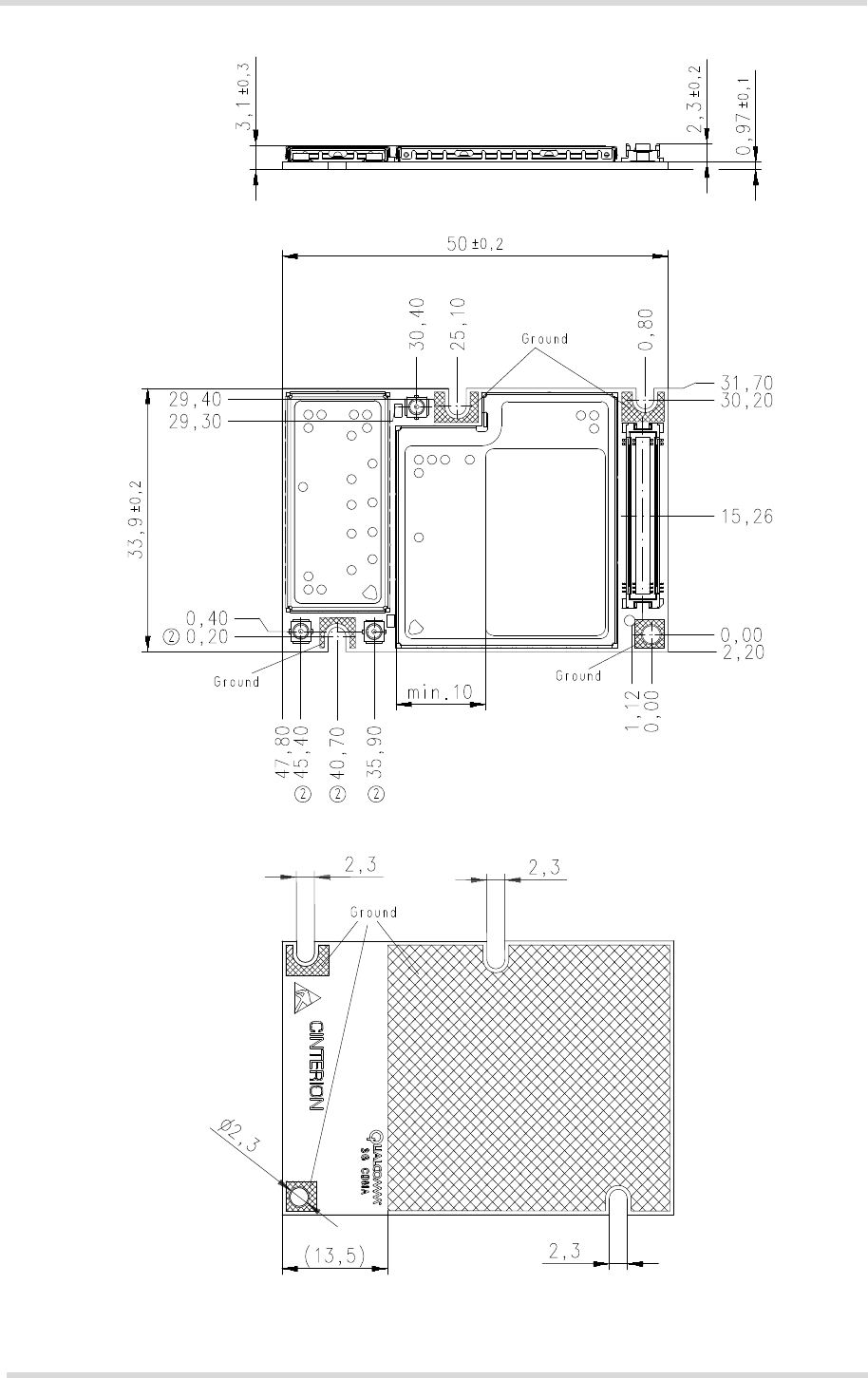
6.1 Mechanical Dimensions of PH8/PH8-P
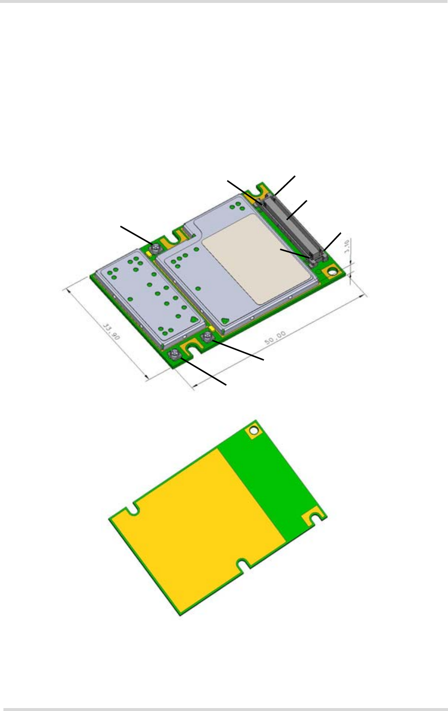
Figure 9 shows the top view of PH8/PH8-P and provides an overview of the board's mechanical
dimensions. For further details see Figure 10.
Length: 50.00mm
Width: 33.90mm
Height: 3.10mm
Figure 9: PH8/PH8-P – top and bottom view
GSM/UMTS antenna
GPS antenna
UMTS diversity antenna
Pin 1 Pin 80
Pin 41
Pin 40
Top view
Bottom view
Application interface
(board-to-board connector)
PH8/PH8-P Hardware Interface Overview
6.2 Mounting PH8/PH8-P to the Application Platform
40
PH8_PH8-P_HD_v02.000 Page 37 of 46 2011-10-21
Confidential / Released
6.2 Mounting PH8/PH8-P to the Application Platform
There are many ways to properly install PH8/PH8-P in the host device. An efficient approach
is to mount the PH8/PH8-P PCB to a frame, plate, rack or chassis.
Fasteners can be M2 screws plus suitable washers, circuit board spacers, or customized
screws, clamps, or brackets. In addition, the board-to-board connection can also be utilized to
achieve better support.
For proper grounding it is strongly recommended to use large ground plane on the bottom of
board in addition to the five GND pins of the board-to-board connector. The ground plane may
also be used to attach cooling elements, e.g. a heat sink or thermally conductive tape.
To prevent mechanical damage, be careful not to force, bend or twist the module. Be sure it is
positioned flat against the host device.
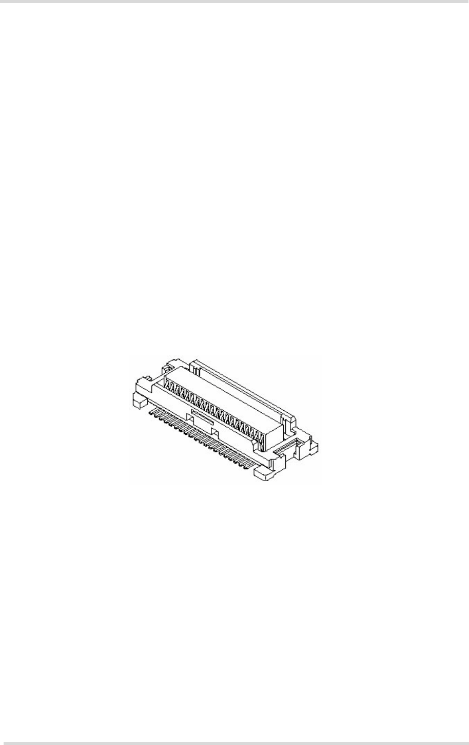
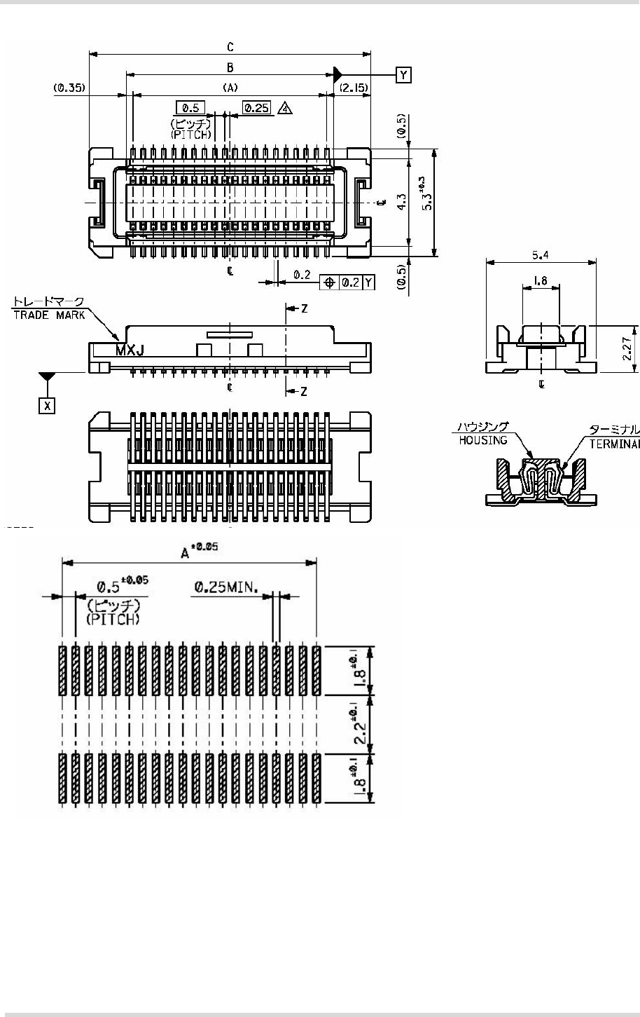
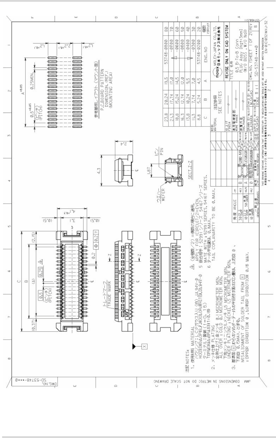
6.3 Board-to-Board Application Connector
This section provides the specifications of the 80-pin board-to-board connector used to connect
PH8/PH8-P to the external application.
Connector mounted on the PH8/PH8-P module:
Type: 52991-0808 SlimStack Receptacle 80 pins, 0.50mm pitch, for stacking heights of
3.0 or 4.0mm, see Figure 12 for details.
Supplier: Molex, http//www.molex.com
PH8/PH8-P Hardware Interface Overview
6.3 Board-to-Board Application Connector
40
PH8_PH8-P_HD_v02.000 Page 38 of 46 2011-10-21
Confidential / Released
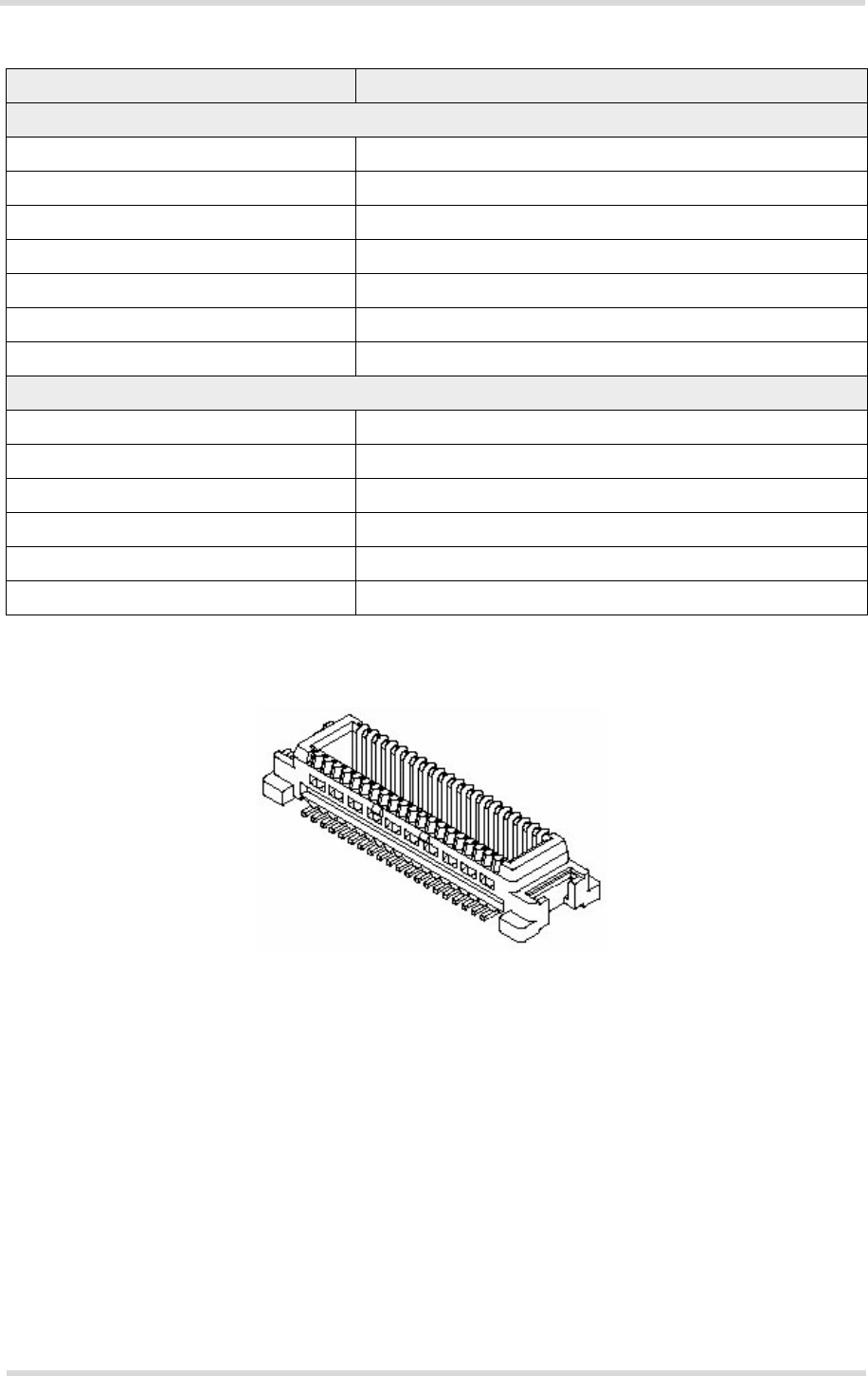
Mating connector types for the customer's application offered by Molex:
Figure 11: Mating board-to-board connector 53748-0808 on application
• 53748-0808 SlimStack Plug, 3mm stacking height,
see Figure 13 for details.
• 53916-0808 SlimStack Plug, 4mm stacking height
Note: There is no inverse polarity protection for the board-to-board connector. It is therefore
very important that the board-to-board connector is connected correctly to the host application,
i.e., pin1 must be connected to pin1, pin2 to pin 2, etc. Pin locations are shown in Figure 9.
Table 14: Technical specifications of Molex board-to-board connector
Parameter Specification (80-pin B2B connector)
Electrical
Number of Contacts 80
Contact spacing 0.5mm (.020")
Voltage 50V
Rated current 0.5A max per contact
Contact resistance 50m max per contact
Insulation resistance > 100M
Dielectric Withstanding Voltage 500V AC (for 1 minute)
Physical
Insulator material (housing) White glass-filled LCP plastic, flammability UL 94V 0
Contact material Plating: Gold over nickel
Insertion force 1st < 74.4N
Insertion force 30th < 65.6N
Withdrawal force 1st > 10.8N
Maximum connection cycles 30 (@ 70m max per contact)

PH8/PH8-P Hardware Interface Overview
7 Sample Application
42
PH8_PH8-P_HD_v02.000 Page 41 of 46 2011-10-21
Confidential / Released
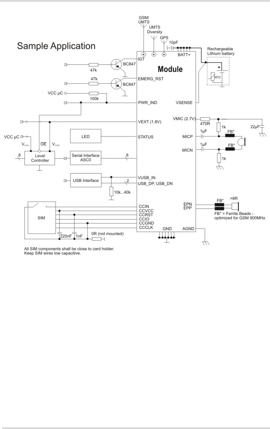
7 Sample Application
Figure 14 shows a typical example of how to integrate an PH8/PH8-P module with an applica-
tion.
The audio interface demonstrates the balanced connection of microphone and earpiece. This
solution is particularly well suited for internal transducers.
The PWR_IND line is an open collector that needs an external pull-up resistor which connects
to the voltage supply VCC µC of the microcontroller. Low state of the open collector pulls the
PWR_IND signal low and indicates that the PH8/PH8-P module is active, high level notifies the
Power-down mode.
If the module is in Power-down mode avoid current flowing from any other source into the mod-
ule circuit, for example reverse current from high state external control lines. Therefore, the
controlling application must be designed to prevent reverse flow. If an external level controller
is required, this can be done by using for example a 5V I/O tolerant buffer/driver like a
"74AVC4T245" with OE (Output Enable) controlled by PWR_IND.
The EMC measures are best practice recommendations. In fact, an adequate EMC strategy for
an individual application is very much determined by the overall layout and, especially, the po-
sition of components.
Disclaimer:
No warranty, either stated or implied, is provided on the sample schematic diagram shown in
Figure 14 and the information detailed in this section. As functionality and compliance with na-
tional regulations depend to a great amount on the used electronic components and the indi-
vidual application layout manufacturers are required to ensure adequate design and operating
safeguards for their products using PH8/PH8-P modules.
PH8/PH8-P Hardware Interface Overview
8 Reference Approval
44
PH8_PH8-P_HD_v02.000 Page 43 of 46 2011-10-21
Confidential / Released
8 Reference Approval
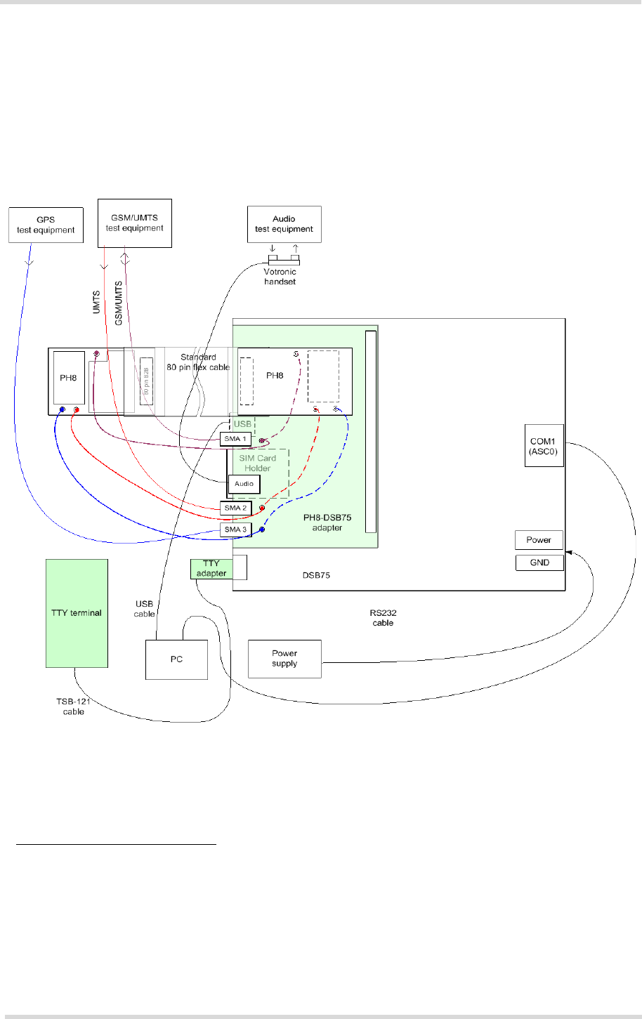
8.1 Reference Equipment for Type Approval
The Cinterion Wireless Modules reference setup submitted to type approve PH8/PH8-P is
shown in the following figure1. The module is connected to the DSB75 via a special adapter
and either mounted directly onto the adapter or connected using a flex cable:
Figure 15: Reference equipment for type approval
1. For RF performance tests a mini-SMT/U.FL to SMA adapter with attached 6dB coaxial attenuator is cho-
sen to connect the module directly to the GSM/UMTS/GPS test equipment instead of employing the SMA
antenna connectors on the PH8/PH8-P-DSB75 adapter as shown in Figure 15. The following products
are recommended:
Hirose SMA-Jack/U.FL-Plug conversion adapter HRMJ-U.FLP(40)
(for details see see http://www.hirose-connectors.com/ or http://www.farnell.com/
Aeroflex Weinschel Fixed Coaxial Attenuator Model 3T/4T
(for details see http://www.aeroflex.com/ams/weinschel/pdfiles/wmod3&4T.pdf)

PH8/PH8-P Hardware Interface Overview
8.2 Compliance with FCC and IC Rules and Regulations
44
PH8_PH8-P_HD_v02.000 Page 44 of 46 2011-10-21
Confidential / Released
8.2 Compliance with FCC and IC Rules and Regulations
The Equipment Authorization Certification for the Cinterion Wireless Modules reference appli-
cation described in Section 8.1 will be registered under the following identifiers:
•PH8:
FCC Identifier QIPPH8
Industry Canada Certification Number: 7830A-PH8
Granted to Cinterion Wireless Modules GmbH
•PH8-P:
FCC Identifier QIPPH8-P
Industry Canada Certification Number: 7830A-PH8P
Granted to Cinterion Wireless Modules GmbH
Manufacturers of mobile or fixed devices incorporating PH8/PH8-P modules are authorized to
use the FCC Grants and Industry Canada Certificates of the PH8/PH8-P modules for their own
final products according to the conditions referenced in these documents. In this case, the FCC
label of the module shall be visible from the outside, or the host device shall bear a second label
stating "Contains FCC ID QIPPH8" resp. "Contains FCC ID QIPPH8-P", and accordingly “Con-
tains IC 7830A-PH8“ resp. “Contains IC 7830A-PH8P“. The integration is limited to fixed or mo-
bile categorised host devices, where a separation distance between the antenna and any
person of min. 20cm can be assured during normal operating conditions. For mobile and fixed
operation configurations the antenna gain, including cable loss, must not exceed the limits that
are stated on the FCC Grant.
IMPORTANT:
Manufacturers of portable applications incorporating PH8/PH8-P modules are required to have
their final product certified and apply for their own FCC Grant and Industry Canada Certificate
related to the specific portable mobile. This is mandatory to meet the SAR requirements for por-
table mobiles.
Changes or modifications not expressly approved by the party responsible for compliance
could void the user's authority to operate the equipment.
Note: This equipment has been tested and found to comply with the limits for a Class B digital
device, pursuant to part 15 of the FCC Rules. These limits are designed to provide reasonable
protection against harmful interference in a residential installation. This equipment generates,
uses and can radiate radio frequency energy and, if not installed and used in accordance with
the instructions, may cause harmful interference to radio communications. However, there is
no guarantee that interference will not occur in a particular installation. If this equipment does
cause harmful interference to radio or television reception, which can be determined by turning
the equipment off and on, the user is encouraged to try to correct the interference by one or
more of the following measures:
• Reorient or relocate the receiving antenna.
• Increase the separation between the equipment and receiver.
• Connect the equipment into an outlet on a circuit different from that to which the receiver
is connected.
• Consult the dealer or an experienced radio/TV technician for help.

PH8/PH8-P Hardware Interface Overview
9 Appendix
46
PH8_PH8-P_HD_v02.000 Page 45 of 46 2011-10-21
Confidential / Released
9 Appendix
9.1 List of Parts and Accessories
Table 15: List of parts and accessories
Description Supplier Ordering information
PH8 Cinterion Standard module
Cinterion Wireless Modules IMEI:
Ordering number: L30960-N1900-A200
Customer IMEI:
Ordering number: L30960-N1905-A200
PH8-P Cinterion Standard module
Cinterion Wireless Modules IMEI:
Ordering number: L30960-N1910-A200
Customer IMEI:
Ordering number: L30960-N1915-A200
DSB75 Support Box Cinterion Ordering number: L36880-N8811-A100
DSB75 adapter for mounting
the PH8/PH8-P evaluation
module
Cinterion Ordering number: L30960-N1802-A100
Votronic Handset VOTRONIC Votronic HH-SI-30.3/V1.1/0
VOTRONIC
Entwicklungs- und Produktionsgesellschaft für elek-
tronische Geräte mbH
Saarbrücker Str. 8
66386 St. Ingbert
Germany
Phone: +49-(0)6 89 4 / 92 55-0
Fax: +49-(0)6 89 4 / 92 55-88
Email: contact@votronic.com
SIM card holder incl. push
button ejector and slide-in
tray
Molex Ordering numbers: 91228
91236
Sales contacts are listed in Table 16.
Board-to-board connector Molex Sales contacts are listed in Table 16.
U.FL antenna connector Hirose or Molex Sales contacts are listed in Table 16 and Table 17.

PH8/PH8-P Hardware Interface Overview
9.1 List of Parts and Accessories
46
PH8_PH8-P_HD_v02.000 Page 46 of 46 2011-10-21
Confidential / Released
Table 16: Molex sales contacts (subject to change)
Molex
For further information please click:
http://www.molex.com
Molex Deutschland GmbH
Felix-Wankel-Str. 11
4078 Heilbronn-Biberach
Germany
Phone: +49-7066-9555 0
Fax: +49-7066-9555 29
Email: mxgermany@molex.com
American Headquarters
Lisle, Illinois 60532
U.S.A.
Phone: +1-800-78MOLEX
Fax: +1-630-969-1352
Molex China Distributors
Beijing,
Room 1319, Tower B, COFCO Plaza
No. 8, Jian Guo Men Nei Street, 100005
Beijing
P.R. China
Phone: +86-10-6526-9628
Phone: +86-10-6526-9728
Phone: +86-10-6526-9731
Fax: +86-10-6526-9730
Molex Singapore Pte. Ltd.
Jurong, Singapore
Phone: +65-268-6868
Fax: +65-265-6044
Molex Japan Co. Ltd.
Yamato, Kanagawa,
Japan
Phone: +81-462-65-2324
Fax: +81-462-65-2366
Table 17: Hirose sales contacts (subject to change)
Hirose Ltd.
For further information please click:
http://www.hirose.com
Hirose Electric (U.S.A.) Inc
2688 Westhills Court
Simi Valley, CA 93065
U.S.A.
Phone: +1-805-522-7958
Fax: +1-805-522-3217
Hirose Electric GmbH
Herzog-Carl-Strasse 4
73760 Ostfildern
Germany
Phone: +49-711-456002-1
Fax: +49-711-456002-299
Email: info@hirose.de
Hirose Electric UK, Ltd
Crownhill Business Centre
22 Vincent Avenue, Crownhill
Milton Keynes, MK8 OAB
Great Britain
Phone: +44-1908-305400
Fax: +44-1908-305401
Hirose Electric Co., Ltd.
5-23, Osaki 5 Chome,
Shinagawa-Ku
Tokyo 141
Japan
Phone: +81-03-3491-9741
Fax: +81-03-3493-2933
Hirose Electric Co., Ltd.
European Branche
First class Building 4F
Beechavenue 46
1119PV Schiphol-Rijk
Netherlands
Phone: +31-20-6557-460
Fax: +31-20-6557-469