THALES DIS AlS Deutschland PHS8-P GSM/GPRS/UMTS/HSPA Module User Manual hio
Gemalto M2M GmbH GSM/GPRS/UMTS/HSPA Module hio
UserManual.wiki
>
THALES DIS AlS Deutschland
>
PHS8-P User Manual
>
User Manual
Contents
1.
User Manual
2.
user manual
User Manual
Navigation menu
Upload a User Manual
Namespaces
Wiki Guide
HTML
PDF
Info
Views
User Manual
Discussion / Help
Navigation
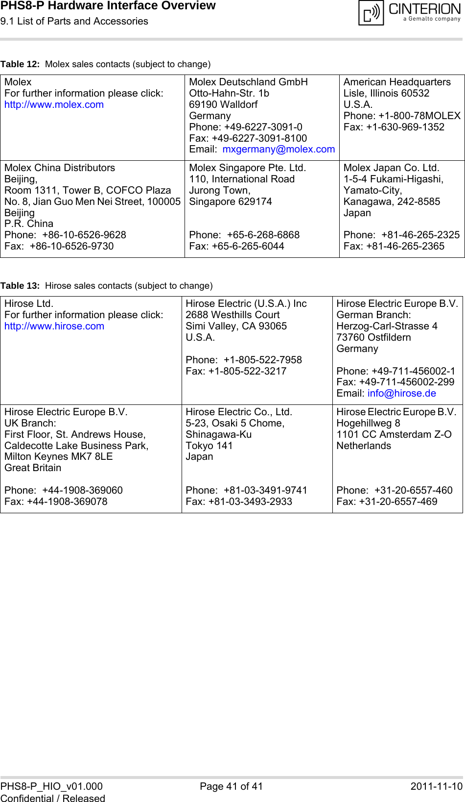
![PHS8-P Hardware Interface Overview1 Introduction15PHS8-P_HIO_v01.000 Page 6 of 111 2011-11-10Confidential / Released1 IntroductionThe document1 describes the hardware of the PHS8-P module, designed to connect to a cel-lular device application and the air interface. It helps you quickly retrieve interface specifica-tions, electrical and mechanical details and information on the requirements to be considered for integrating further components.1.1 Related Documents[1] PHS8-P AT Command Set[2] PHS8-P Release Notes[3] DSB75 Support Box - Evaluation Kit for Cinterion Wireless Modules[4] Application Note 48: SMT Module Integration1.2 Terms and Abbreviations1. The document is effective only if listed in the appropriate Release Notes as part of the technicaldocumentation delivered with your Cinterion Wireless Modules product.Abbreviation DescriptionAGPS Assisted GPSANSI American National Standards InstituteAMR Adaptive MultirateARP Antenna Reference PointBB BasebandBEP Bit Error ProbabilityBTS Base Transceiver StationCB or CBM Cell Broadcast MessageCE Conformité Européene (European Conformity)CS Coding SchemeCS Circuit SwitchedCSD Circuit Switched DataCTM Cellular Text ModemDAC Digital-to-Analog ConverterDCS Digital Cellular SystemDL DownloadDRX Discontinuous ReceptionDSB Development Support Board](https://usermanual.wiki/THALES-DIS-AlS-Deutschland/PHS8-P.User-Manual/User-Guide-1597398-Page-6.png)
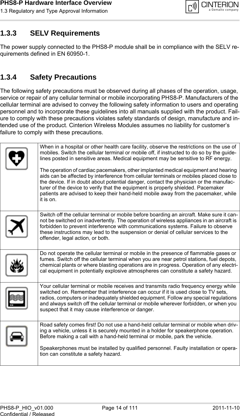
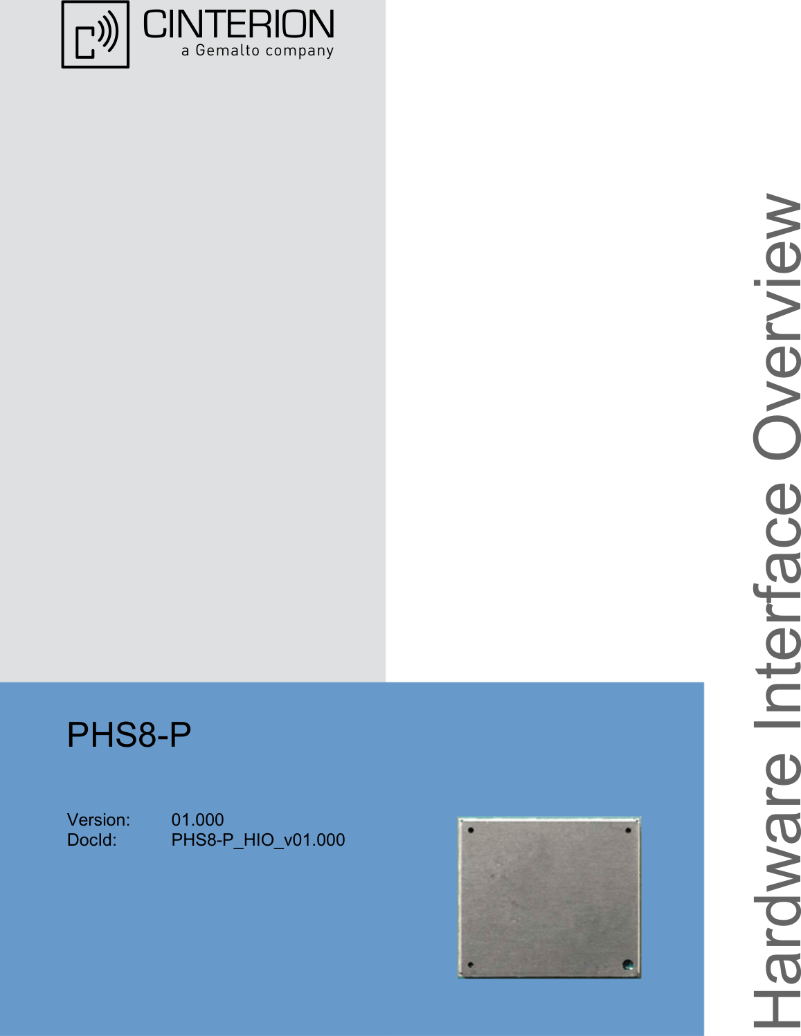
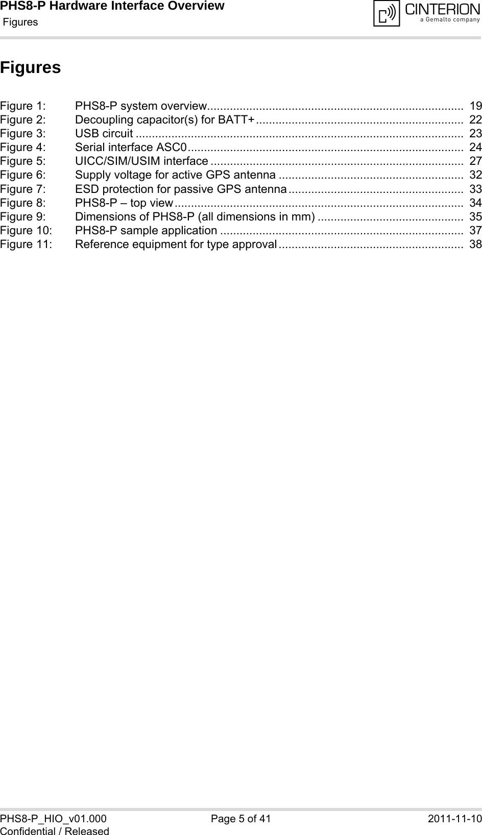
![PHS8-P Hardware Interface Overview2.1 Key Features at a Glance19PHS8-P_HIO_v01.000 Page 18 of 41 2011-11-10Confidential / ReleasedInterfacesModule interface Surface mount device with solderable connection pads (SMT application interface).Land grid array (LGA) technology ensures high solder joint reliability and provides the possibility to use an optional module mounting socket.For more information on how to integrate SMT modules see also [11]. This application note comprises chapters on module mounting and appli-cation layout issues as well as on additional SMT application develop-ment equipment.Antenna 50Ohms. Main GSM/UMTS antenna, UMTS diversity antenna, GPS antenna (active/passive) USB USB 2.0 High Speed (480Mbit/s) device interface, Full Speed (12Mbit/s) compliantSerial interface ASC0:• 8-wire modem interface with status and control lines, unbalanced,asynchronous• Adjustable baud rates from 9,600bps up to 921,600bps• Supports RTS0/CTS0 hardware flow control• Multiplex ability according to GSM 07.10 Multiplexer ProtocolUICC interface Supported chip cards: UICC/SIM/USIM 3V, 1.8VStatus Signal line to indicate network connectivity stateAudio 1 analog interface with microphone feeding1 digital interface: PCM or I2SPower on/off, ResetPower on/off Switch-on by hardware signal IGTSwitch-off by AT command (AT^SMSO)Automatic switch-off in case of critical temperature or voltage conditionsReset Orderly shutdown and reset by AT commandEmergency-off Emergency-off by hardware signal EMERG_OFF if IGT is not activeSpecial FeaturesPhonebook SIM and phoneTTY/CTM support Integrated CTM modemAntenna SAIC (Single Antenna Interference Cancellation) / DARP (Downlink Advanced Receiver Performance)Rx diversity (receiver type 3i - 16-QAM)1Evaluation kitEvaluation module PHS8-P module soldered onto a dedicated PCB that can be connected to an adapter in order to be mounted onto the DSB75.DSB75 DSB75 Development Support Board designed to test and type approve Cinterion Wireless Modules and provide a sample configuration for appli-cation engineering. A special adapter is required to connect the PHS8-P evaluation module to the DSB75.1. UMTS Rx diversity antenna does not support UMTS/HSPA+ band VIII. Feature Implementation](https://usermanual.wiki/THALES-DIS-AlS-Deutschland/PHS8-P.User-Manual/User-Guide-1597398-Page-18.png)
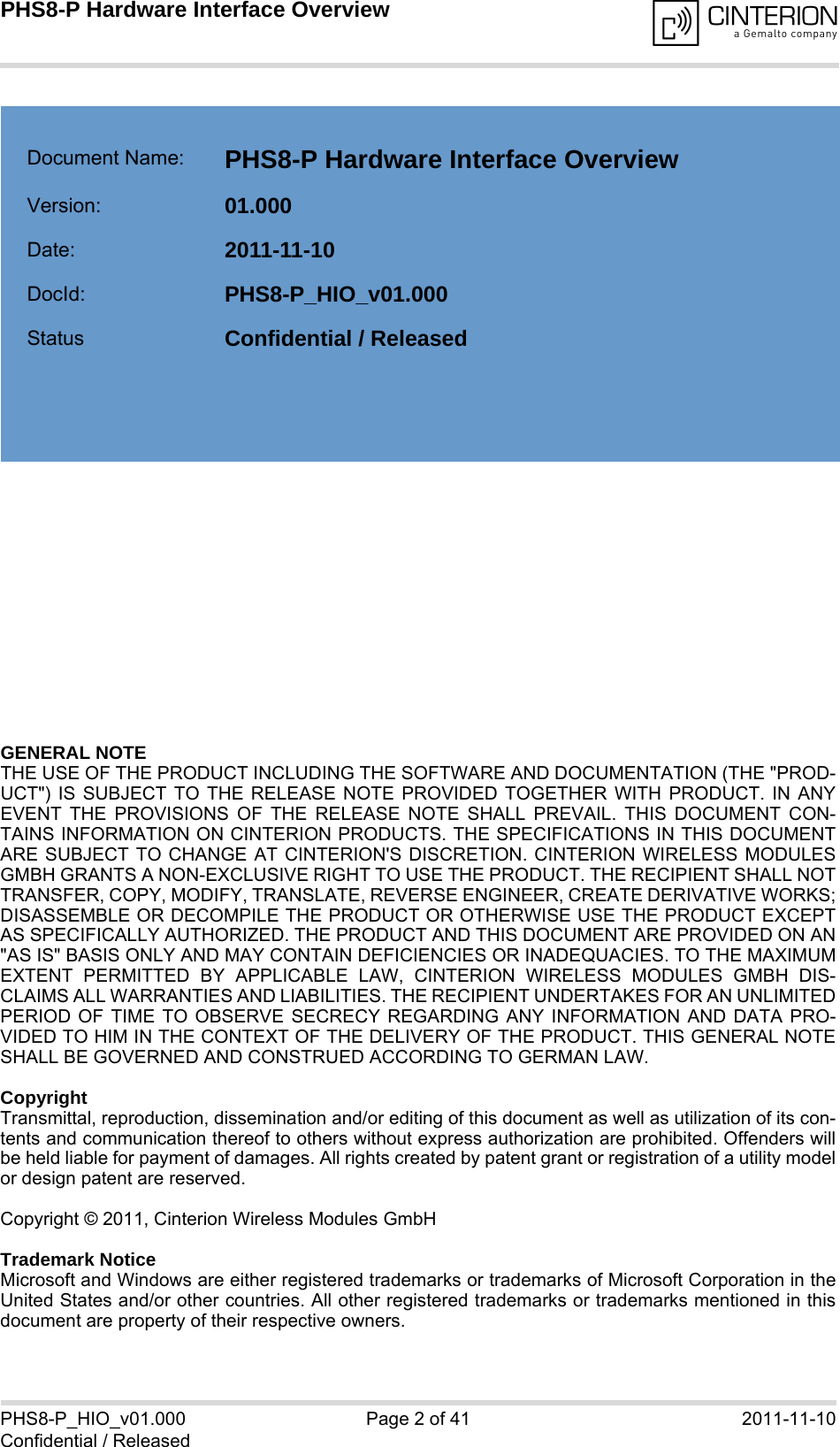
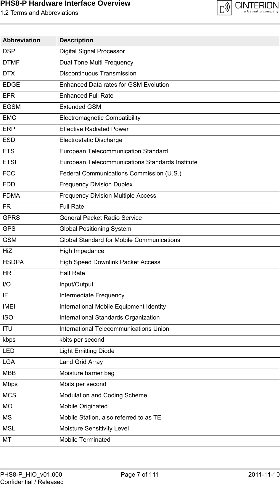
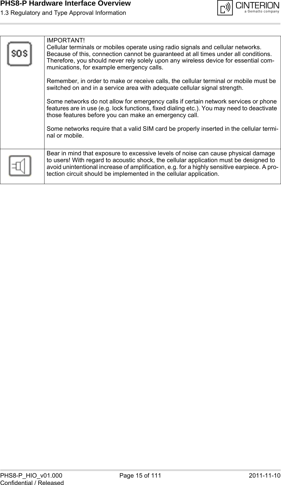
![PHS8-P Hardware Interface Overview5 Antenna Interfaces33PHS8-P_HIO_v01.000 Page 30 of 41 2011-11-10Confidential / Released5 Antenna Interfaces5.1 GSM/UMTS Antenna InterfaceThe PHS8-P GSM/UMTS antenna interface comprises a main GSM/UMTS antenna as well as an optional UMTS Rx diversity antenna to improve signal reliability and quality1. The interface has an impedance of 50Ω. PHS8-P is capable of sustaining a total mismatch at the antenna interface without any damage, even when transmitting at maximum RF power.The external antenna must be matched properly to achieve best performance regarding radi-ated power, modulation accuracy and harmonic suppression. Matching networks are not in-cluded on the PHS8-P PCB and should be placed in the host application, if the antenna does not have an impendance of 50Ω.Regarding the return loss PHS8-P provides the following values in the active band:1. By delivery default the optional UMTS Rx diversity antenna is configured as available for the module. Toavoid negative side effects and performance degradation it is recommended to disable the diversity an-tenna path if - the host application does not support a diversity antenna- the host application includes a diversity antenna - but a 3G network simulator is used for developmentand performance tests.Please refer to [1] for details on how to configure antenna settings. Table 10: Return loss in the active bandState of module Return loss of module Recommended return loss of applicationReceive > 8dB > 12dBTransmit not applicable > 12dBIdle < 5dB not applicable](https://usermanual.wiki/THALES-DIS-AlS-Deutschland/PHS8-P.User-Manual/User-Guide-1597398-Page-30.png)
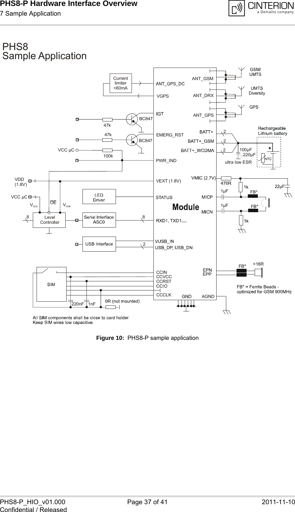
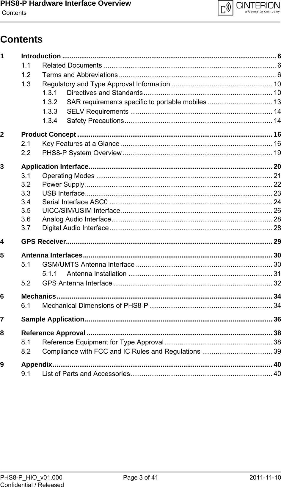
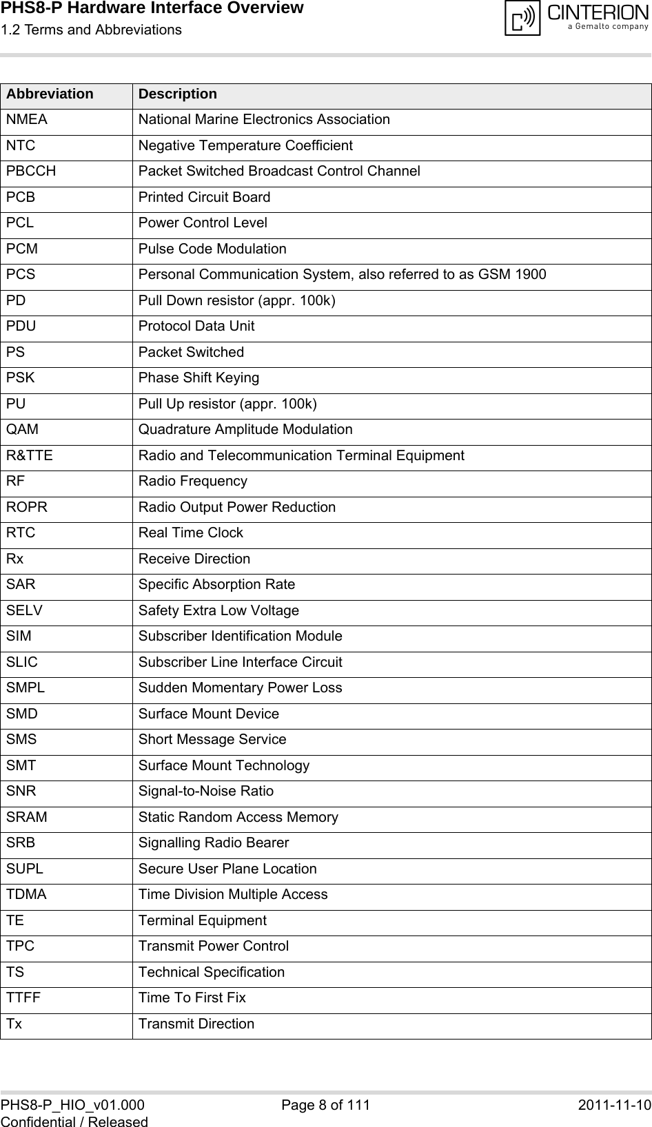
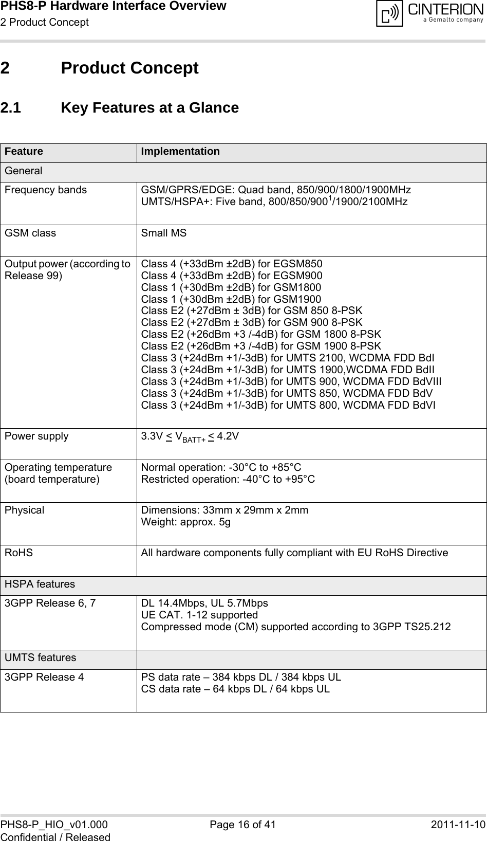
![PHS8-P Hardware Interface Overview7 Sample Application37PHS8-P_HIO_v01.000 Page 36 of 41 2011-11-10Confidential / Released7 Sample ApplicationFigure 10 shows a typical example of how to integrate an PHS8-P module with an application. The audio interface demonstrates the balanced connection of microphone and earpiece. This solution is particularly well suited for internal transducers.The PWR_IND line is an open collector that needs an external pull-up resistor which connects to the voltage supply VCC µC of the microcontroller. Low state of the open collector pulls the PWR_IND signal low and indicates that the PHS8-P module is active, high level notifies the Power-down mode. If the module is in Power-down mode avoid current flowing from any other source into the mod-ule circuit, for example reverse current from high state external control lines. Therefore, the controlling application must be designed to prevent reverse flow. If an external level controller is required, this can be done by using for example a 5V I/O tolerant buffer/driver like a "74AVC4T245" with OE (Output Enable) controlled by PWR_IND.While developing SMT applications it is strongly recommended to provide test pointsfor certain signals resp. lines to and from the module - for debug and/or test purposes.The SMT application should allow for an easy access to these signals. For details onhow to implement test points see [4].The EMC measures are best practice recommendations. In fact, an adequate EMC strategy for an individual application is very much determined by the overall layout and, especially, the po-sition of components. Disclaimer:No warranty, either stated or implied, is provided on the sample schematic diagram shown in Figure 10 and the information detailed in this section. As functionality and compliance with na-tional regulations depend to a great amount on the used electronic components and the indi-vidual application layout manufacturers are required to ensure adequate design and operating safeguards for their products using PHS8-P modules.](https://usermanual.wiki/THALES-DIS-AlS-Deutschland/PHS8-P.User-Manual/User-Guide-1597398-Page-36.png)