THALES DIS AlS Deutschland PLS62-W LTE Data-Only SMT World-Module User Manual pls62 w hid
Gemalto M2M GmbH LTE Data-Only SMT World-Module pls62 w hid
UserManual.wiki
>
THALES DIS AlS Deutschland
>
PLS62-W User Manual
>
pls62-w_hio
Contents
1.
pls62-w_hio
2.
User Manual
pls62-w_hio
Navigation menu
Upload a User Manual
Namespaces
Wiki Guide
HTML
PDF
Info
Views
User Manual
Discussion / Help
Navigation
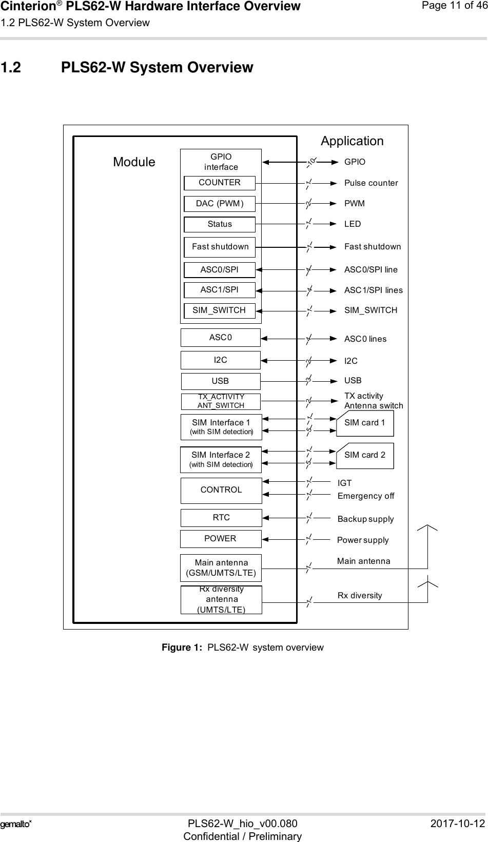
![Cinterion® PLS62-W Hardware Interface Overview1.1 Key Features at a Glance11PLS62-W_hio_v00.080 2017-10-12Confidential / PreliminaryPage 9 of 46Java™ Open Platform Java™ Open Platform with • Java™ profile IMP-NG & CLDC 1.1 HI• Secure data transmission via HTTPS/SSL1• Multi-threading programming and multi-application executionMajor benefits: seamless integration into Java applications, ease of pro-gramming, no need for application microcontroller, extremely cost-efficient hardware and software design – ideal platform for industrial applications.The memory space available for Java programs is 30MB in the flash file system and 18MB RAM. Application code and data share the space in the flash file system and in RAM.Microsoft™ compatibility RIL for Pocket PC and Smartphone SIM Application Toolkit SAT letter classes b, c, e; with BIPFirmware update Generic update from host application over ASC0 or USB modem.InterfacesModule interface Surface mount device with solderable connection pads (SMT application interface). Land grid array (LGA) technology ensures high solder joint reli-ability and allows the use of an optional module mounting socket.For more information on how to integrate SMT modules see also [3]. This application note comprises chapters on module mounting and application layout issues as well as on additional SMT application development equip-ment.USB USB 2.0 High Speed (480Mbit/s) device interface, Full Speed (12Mbit/s)compliant2 serial interfaces ASC0 (in parts shared with GPIO lines):• 8-wire modem interface with status and control lines, unbalanced, asyn-chronous• Adjustable baud rates: 1,200bps to 921,600bps• Autobauding: 1,200bps to 230,400bps• Supports RTS0/CTS0 hardware flow control.ASC1 (shared with GPIO lines):• 4-wire, unbalanced asynchronous interface• Adjustable baud rates: 1,200bps to 921,600bps• Autobauding: 1,200bps to 230,400bps• Supports RTS1/CTS1 hardware flow controlUICC interface Supported SIM/USIM cards: 3V, 1.8V GPIO interface 24 GPIO lines comprising: 14 lines shared with ASC0, ASC1 and SPI lines, with network status indica-tion, PWM functionality, fast shutdown, pulse counter, and SIM switch10 GPIO lines not sharedI2C interface Supports I2C serial interfaceSPI interface Serial peripheral interface, shared with GPIO linesAntenna switch interface Control signal for 700MHz antenna switchTX activity interface Signal indicating 2G/3G/4G transmit activitiesAntenna interface pads 50Ω. UMTS/GSM/LTE main antenna, UMTS/LTE Rx Diversity antennaFeature Implementation](https://usermanual.wiki/THALES-DIS-AlS-Deutschland/PLS62-W.pls62-w-hio/User-Guide-3603185-Page-9.png)
![Cinterion® PLS62-W Hardware Interface Overview2.1 Application Interface28PLS62-W_hio_v00.080 2017-10-12Confidential / PreliminaryPage 17 of 462.1.5 GPIO InterfacePLS62-W offers a GPIO interface with 24 GPIO lines. The GPIO lines are shared with otherinterfaces or functions: Fast shutdown (see Section 2.1.10.1), status LED (see Section 2.1.10),the PWM functionality (see Section 2.1.8), an pulse counter (see Section 2.1.9), ASC0 (seeSection 2.1.2), ASC1 (see Section 2.1.3), an SPI interface (see Section 2.1.7). The following table shows the configuration variants for the GPIO pads. All variants are mutu-ally exclusive, i.e. a pad configured for instance as Status LED is locked for alternative usage.After startup, the above mentioned alternative GPIO line assignments can be configured usingAT commands (see [1]). The configuration is non-volatile and available after module restart.Table 2: GPIO lines and possible alternative assignmentGPIO Fast Shutdown Status LED PWM Pulse Counter ASC0 ASC1 SPI SIM SWITCHGPIO1 DTR0GPIO2 DCD0GPIO3 DSR0 SPI_CLKGPIO4 FST_SHDNGPIO5 Status LEDGPIO6 PWM2GPIO7 PWM1GPIO8 COUNTERGPIO11GPIO12GPIO13GPIO14GPIO15GPIO16 RXD1 SPI_MOSIGPIO17 TXD1 SPI_MISOGPIO18 RTS1GPIO19 CTS1 SPI_CSGPIO20GPIO21GPIO22GPIO23GPIO24 RING0GPIO25GPIO26 SIM_SWITCH](https://usermanual.wiki/THALES-DIS-AlS-Deutschland/PLS62-W.pls62-w-hio/User-Guide-3603185-Page-17.png)
![Cinterion® PLS62-W Hardware Interface Overview2.2 RF Antenna Interface28PLS62-W_hio_v00.080 2017-10-12Confidential / PreliminaryPage 20 of 462.2 RF Antenna InterfaceThe PLS62-W GSM/UMTS/LTE antenna interface comprises a GSM/UMTS/LTE main antenna as well as a UMTS/LTE Rx diversity antenna to improve signal reliability and quality1. The RF interface has an impedance of 50Ω. PLS62-W is capable of sustaining a total mismatch at the antenna line without any damage, even when transmitting at maximum RF power.The external antenna must be matched properly to achieve best performance regarding radi-ated power, modulation accuracy and harmonic suppression. Antenna matching networks are not included on the PLS62-W module and should be placed in the host application if the anten-na does not have an impedance of 50Ω.Regarding the return loss PLS62-W provides the following values in the active band:1. By delivery default the UMTS/LTE Rx diversity antenna is configured as available for the module sinceits usage is mandatory for LTE. Please refer to [1] for details on how to configure antenna settings.Table 3: Return loss in the active bandState of module Return loss of module Recommended return loss of applicationReceive > 8dB > 12dBTransmit not applicable > 12dB](https://usermanual.wiki/THALES-DIS-AlS-Deutschland/PLS62-W.pls62-w-hio/User-Guide-3603185-Page-20.png)
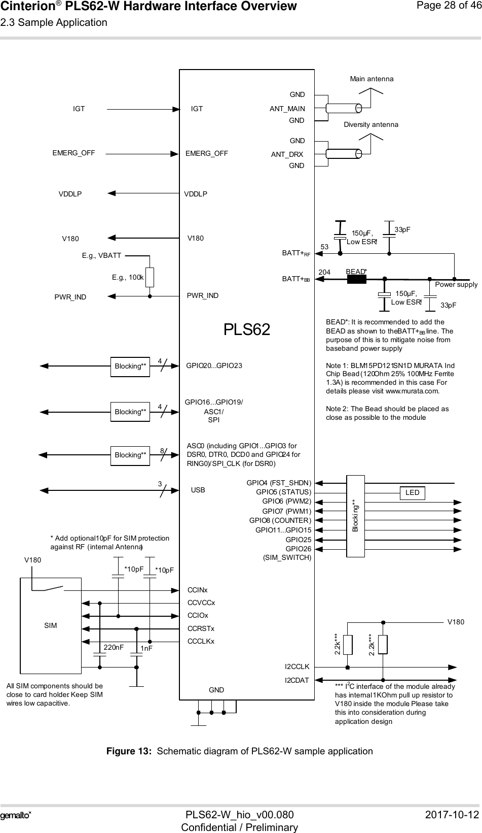
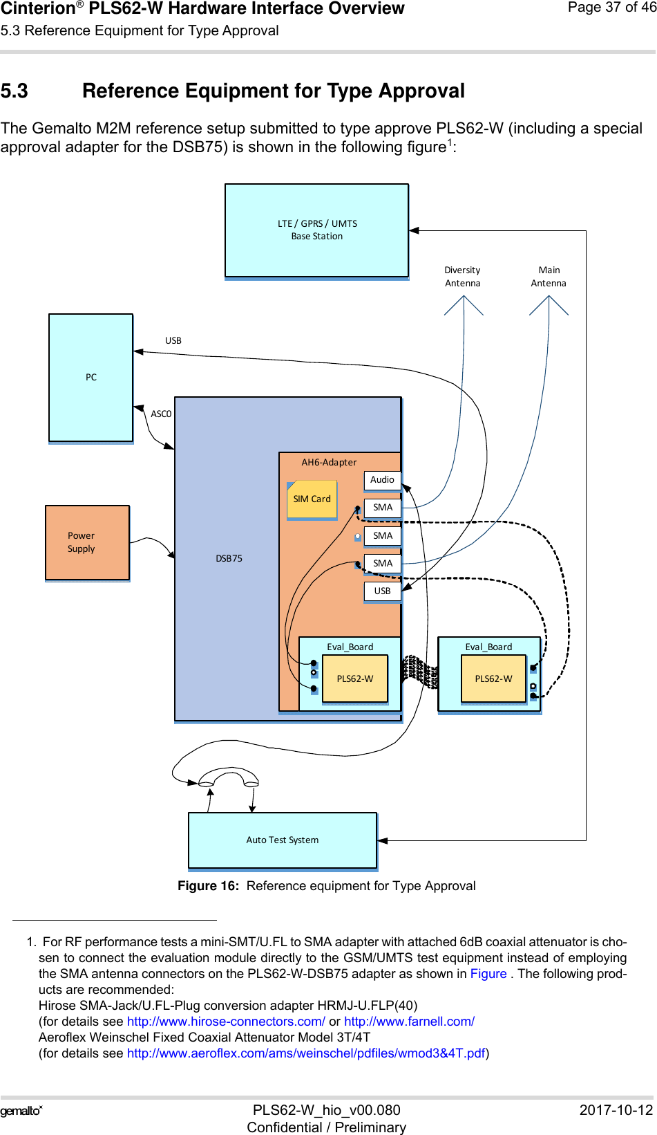
![Cinterion® PLS62-W Hardware Interface Overview2.3 Sample Application28PLS62-W_hio_v00.080 2017-10-12Confidential / PreliminaryPage 27 of 462.3 Sample ApplicationFigure 13 shows a typical example of how to integrate a PLS62-W module with an application.Usage of the various host interfaces depends on the desired features of the application.Because of the very low power consumption design, current flowing from any other source intothe module circuit must be avoided, for example reverse current from high state external controllines. Therefore, the controlling application must be designed to prevent reverse current flow.Otherwise there is the risk of undefined states of the module during startup and shutdown oreven of damaging the module.Because of the high RF field density inside the module, it cannot be guaranteed that no selfinterference might occur, depending on frequency and the applications grounding concept. Thepotential interferers may be minimized by placing small capacitors (47pF) at suspected lines(e.g. RXD0, VDDLP, and ON). While developing SMT applications it is strongly recommended to provide test pointsfor certain signals, i.e., lines to and from the module - for debug and/or test purposes.The SMT application should allow for an easy access to these signals. For details onhow to implement test points see [3].The EMC measures are best practice recommendations. In fact, an adequate EMC strategy foran individual application is very much determined by the overall layout and, especially, the po-sition of components. Note: PLS62-W is not intended for use with cables longer than 3m.DisclaimerNo warranty, either stated or implied, is provided on the sample schematic diagram shown inFigure 13 and the information detailed in this section. As functionality and compliance with na-tional regulations depend to a great amount on the used electronic components and the indi-vidual application layout manufacturers are required to ensure adequate design and operatingsafeguards for their products using PLS62-W modules.](https://usermanual.wiki/THALES-DIS-AlS-Deutschland/PLS62-W.pls62-w-hio/User-Guide-3603185-Page-27.png)
![Cinterion® PLS62-W Hardware Interface Overview3 Operating Characteristics30PLS62-W_hio_v00.080 2017-10-12Confidential / PreliminaryPage 29 of 463 Operating Characteristics3.1 Operating ModesThe table below briefly summarizes the various operating modes referred to throughout the document.Mode FunctionNormal operationGSM / GPRS / UMTS / HSPA / LTE SLEEPPower saving set automatically when no call is in progress and the USB connection is suspended by host or not present and no active commu-nication via ASC0. GSM / GPRS / UMTS / HSPA / LTE IDLEPower saving disabled or an USB connection not suspended, but no call in progress.GSM TALK/GSM DATAConnection between two subscribers is in progress. Power consump-tion depends on the GSM network coverage and several connection settings (e.g. DTX off/on, FR/EFR/HR, hopping sequences and antenna connection). The following applies when power is to be mea-sured in TALK_GSM mode: DTX off, FR and no frequency hopping.GPRS DATA GPRS data transfer in progress. Power consumption depends on net-work settings (e.g. power control level), uplink / downlink data rates and GPRS configuration (e.g. used multislot settings).EGPRS DATA EGPRS data transfer in progress. Power consumption depends on net-work settings (e.g. power control level), uplink / downlink data rates and EGPRS configuration (e.g. used multislot settings).UMTS TALK/UMTS DATAUMTS data transfer in progress. Power consumption depends on net-work settings (e.g. TPC Pattern) and data transfer rate.HSPA DATA HSPA data transfer in progress. Power consumption depends on net-work settings (e.g. TPC Pattern) and data transfer rate.LTE DATA LTE data transfer in progress. Power consumption depends on network settings (e.g. TPC Pattern) and data transfer rate.Power DownNormal shutdown after sending the power down command. Only a voltage regulator is active for powering the RTC. Software is not active. Interfaces are not accessible. Operat-ing voltage remains applied.Airplane modeAirplane mode shuts down the radio part of the module, causes the module to log off from the network and disables all AT commands whose execution requires a radio connection.Airplane mode can be controlled by AT command (see [1]).](https://usermanual.wiki/THALES-DIS-AlS-Deutschland/PLS62-W.pls62-w-hio/User-Guide-3603185-Page-29.png)
![Cinterion® PLS62-W Hardware Interface Overview6 Document Information43PLS62-W_hio_v00.080 2017-10-12Confidential / PreliminaryPage 40 of 466 Document Information6.1 Revision HistoryNew document: "Cinterion® PLS62-W Hardware Interface Overview" Version 00.0806.2 Related Documents[1] PLS62-W AT Command Set[2] PLS62-W Release Note[3] Application Note 48: SMT Module Integration[4] Application Note 40: Thermal Solutions[5] Universal Serial Bus Specification Revision 2.0, April 27, 20006.3 Terms and AbbreviationsChapter What is new-- Initial document setup.Abbreviation DescriptionADC Analog-to-digital converterAGC Automatic Gain ControlANSI American National Standards InstituteARFCN Absolute Radio Frequency Channel NumberARP Antenna Reference PointASC0/ASC1 Asynchronous Controller. Abbreviations used for first and second serial interface of PLS62-WB Thermistor ConstantBER Bit Error RateBIP Bearer Independent ProtocolBTS Base Transceiver StationCB or CBM Cell Broadcast MessageCE Conformité Européene (European Conformity)CHAP Challenge Handshake Authentication ProtocolCPU Central Processing UnitCS Coding SchemeCSD Circuit Switched DataCTS Clear to SendDAC Digital-to-Analog Converter](https://usermanual.wiki/THALES-DIS-AlS-Deutschland/PLS62-W.pls62-w-hio/User-Guide-3603185-Page-40.png)