THALES DIS AlS Deutschland PLS62-W LTE Data-Only SMT World-Module User Manual pls62 w hid
Gemalto M2M GmbH LTE Data-Only SMT World-Module pls62 w hid
Contents
- 1. pls62-w_hio
- 2. User Manual
pls62-w_hio
GEMALTO.COM/M2M.
Cinterion® PLS62-W
Hardware Interface Overview
Version: 00.080
DocId: PLS62-W_hio_v00.080

GENERAL NOTE
THE USE OF THE PRODUCT INCLUDING THE SOFTWARE AND DOCUMENTATION (THE "PROD-
UCT") IS SUBJECT TO THE RELEASE NOTE PROVIDED TOGETHER WITH PRODUCT. IN ANY
EVENT THE PROVISIONS OF THE RELEASE NOTE SHALL PREVAIL. THIS DOCUMENT CONTAINS
INFORMATION ON GEMALTO M2M PRODUCTS. THE SPECIFICATIONS IN THIS DOCUMENT ARE
SUBJECT TO CHANGE AT GEMALTO M2M'S DISCRETION. GEMALTO M2M GMBH GRANTS A NON-
EXCLUSIVE RIGHT TO USE THE PRODUCT. THE RECIPIENT SHALL NOT TRANSFER, COPY,
MODIFY, TRANSLATE, REVERSE ENGINEER, CREATE DERIVATIVE WORKS; DISASSEMBLE OR
DECOMPILE THE PRODUCT OR OTHERWISE USE THE PRODUCT EXCEPT AS SPECIFICALLY
AUTHORIZED. THE PRODUCT AND THIS DOCUMENT ARE PROVIDED ON AN "AS IS" BASIS ONLY
AND MAY CONTAIN DEFICIENCIES OR INADEQUACIES. TO THE MAXIMUM EXTENT PERMITTED
BY APPLICABLE LAW, GEMALTO M2M GMBH DISCLAIMS ALL WARRANTIES AND LIABILITIES.
THE RECIPIENT UNDERTAKES FOR AN UNLIMITED PERIOD OF TIME TO OBSERVE SECRECY
REGARDING ANY INFORMATION AND DATA PROVIDED TO HIM IN THE CONTEXT OF THE DELIV-
ERY OF THE PRODUCT. THIS GENERAL NOTE SHALL BE GOVERNED AND CONSTRUED
ACCORDING TO GERMAN LAW.
Copyright
Transmittal, reproduction, dissemination and/or editing of this document as well as utilization of its con-
tents and communication thereof to others without express authorization are prohibited. Offenders will be
held liable for payment of damages. All rights created by patent grant or registration of a utility model or
design patent are reserved.
Copyright © 2017, Gemalto M2M GmbH, a Gemalto Company
Trademark Notice
Gemalto, the Gemalto logo, are trademarks and service marks of Gemalto and are registered in certain
countries. Microsoft and Windows are either registered trademarks or trademarks of Microsoft Corpora-
tion in the United States and/or other countries. All other registered trademarks or trademarks mentioned
in this document are property of their respective owners.
PLS62-W_hio_v00.080 2017-10-12
Confidential / Preliminary
Cinterion® PLS62-W Hardware Interface Overview
2
Page 2 of 46
Document Name: Cinterion® PLS62-W Hardware Interface Overview
Version: 00.080
Date: 2017-10-12
DocId: PLS62-W_hio_v00.080
Status Confidential / Preliminary

Cinterion® PLS62-W Hardware Interface Overview
Contents
46
PLS62-W_hio_v00.080 2017-10-12
Confidential / Preliminary
Page 3 of 46
Contents
1 Introduction ................................................................................................................. 7
1.1 Key Features at a Glance .................................................................................. 7
1.2 PLS62-W System Overview............................................................................. 11
2 Interface Characteristics .......................................................................................... 12
2.1 Application Interface ........................................................................................ 12
2.1.1 USB Interface...................................................................................... 12
2.1.2 Serial Interface ASC0 ......................................................................... 13
2.1.3 Serial Interface ASC1 ......................................................................... 14
2.1.4 UICC/SIM/USIM Interface................................................................... 15
2.1.4.1 SIM Card Interface Switch .................................................. 16
2.1.5 GPIO Interface .................................................................................... 17
2.1.6 I2C Interface ........................................................................................ 18
2.1.7 SPI Interface ....................................................................................... 18
2.1.8 PWM Interfaces .................................................................................. 18
2.1.9 Pulse Counter ..................................................................................... 18
2.1.10 Status LED.......................................................................................... 18
2.1.10.1 Fast Shutdown .................................................................... 19
2.1.11 700MHz Antenna Switch Control ........................................................ 19
2.1.12 TX Activity Signal ................................................................................ 19
2.2 RF Antenna Interface....................................................................................... 20
2.2.1 Antenna Installation ............................................................................ 21
2.2.2 RF Line Routing Design...................................................................... 21
2.2.2.1 Line Arrangement Examples ............................................... 21
2.2.2.2 Routing Example................................................................. 26
2.3 Sample Application .......................................................................................... 27
3 Operating Characteristics ........................................................................................ 29
3.1 Operating Modes ............................................................................................. 29
3.2 Power Supply................................................................................................... 30
4 Mechanical Dimensions, Mounting and Packaging............................................... 31
4.1 Mechanical Dimensions of PLS62-W............................................................... 31
5 Regulatory and Type Approval Information ........................................................... 33
5.1 Directives and Standards................................................................................. 33
5.2 SAR requirements specific to portable mobiles ............................................... 36
5.3 Reference Equipment for Type Approval......................................................... 37
5.4 Compliance with FCC Rules and Regulations ................................................. 38
6 Document Information.............................................................................................. 40
6.1 Revision History ............................................................................................... 40
6.2 Related Documents ......................................................................................... 40
6.3 Terms and Abbreviations ................................................................................. 40
6.4 Safety Precaution Notes .................................................................................. 43

Cinterion® PLS62-W Hardware Interface Overview
Contents
46
PLS62-W_hio_v00.080 2017-10-12
Confidential / Preliminary
Page 4 of 46
7 Appendix.................................................................................................................... 44
7.1 List of Parts and Accessories........................................................................... 44

Cinterion® PLS62-W Hardware Interface Overview
Tables
118
PLS62-W_hio_v00.080 2017-10-12
Confidential / Preliminary
Page 5 of 46
Tables
Table 1: Signals of the SIM interface (SMT application interface) ............................... 15
Table 2: GPIO lines and possible alternative assignment............................................ 17
Table 3: Return loss in the active band........................................................................ 20
Table 4: Directives ....................................................................................................... 33
Table 5: Standards of North American type approval .................................................. 33
Table 6: Standards of European type approval............................................................ 33
Table 7: Requirements of quality ................................................................................. 34
Table 8: Standards of the Ministry of Information Industry of the
People’s Republic of China............................................................................ 34
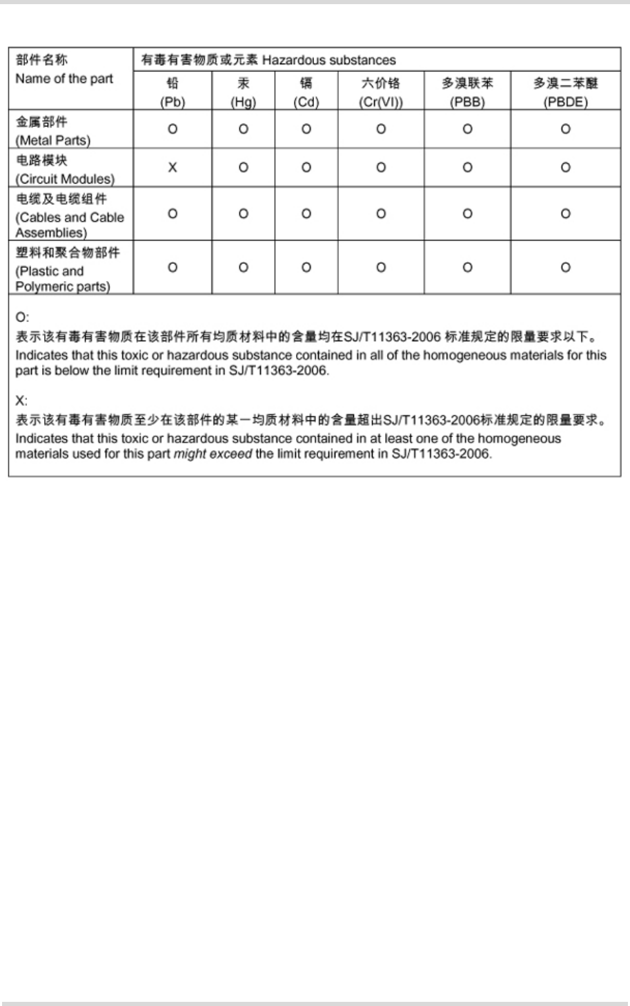
Table 9: Toxic or hazardous substances or elements with defined
concentration limits ........................................................................................ 35
Table 10: Antenna gain limits for FCC and IC (TBD.).................................................... 38
Table 11: List of parts and accessories.......................................................................... 44
Table 12: Molex sales contacts (subject to change) ...................................................... 45

Cinterion® PLS62-W Hardware Interface Overview
Figures
118
PLS62-W_hio_v00.080 2017-10-12
Confidential / Preliminary
Page 6 of 46
Figures
Figure 1: PLS62-W system overview ............................................................................ 11
Figure 2: USB circuit ..................................................................................................... 12
Figure 3: Serial interface ASC0..................................................................................... 13
Figure 4: Serial interface ASC1..................................................................................... 14
Figure 5: UICC/SIM/USIM interfaces ............................................................................ 16
Figure 6: Embedded Stripline with 65µm prepreg (1080) and 710µm core .................. 21
Figure 7: Micro-Stripline on 1.0mm standard FR4 2-layer PCB - example 1 ................ 22
Figure 8: Micro-Stripline on 1.0mm Standard FR4 PCB - example 2............................ 23
Figure 9: Micro-Stripline on 1.5mm Standard FR4 PCB - example 1............................ 24
Figure 10: Micro-Stripline on 1.5mm Standard FR4 PCB - example 2............................ 25
Figure 11: Routing to application‘s RF connector ........................................................... 26
Figure 12: PLS62-W evaluation board layer table........................................................... 26
Figure 13: Schematic diagram of PLS62-W sample application ..................................... 28
Figure 14: PLS62-W– top and bottom view..................................................................... 31
Figure 15: Dimensions of PLS62-W (all dimensions in mm)........................................... 32
Figure 16: Reference equipment for Type Approval ....................................................... 37

Cinterion® PLS62-W Hardware Interface Overview
1 Introduction
11
PLS62-W_hio_v00.080 2017-10-12
Confidential / Preliminary
Page 7 of 46
1 Introduction
This document1 describes the hardware of the Cinterion® PLS62-W module. It helps you quick-
ly retrieve interface specifications, electrical and mechanical details and information on the re-
quirements to be considered for integrating further components.
1.1 Key Features at a Glance
1. The document is effective only if listed in the appropriate Release Notes as part of the technical docu-
mentation delivered with your Gemalto M2M product.
Feature Implementation
General
Frequency bands GSM/GPRS/EDGE: Quad band, 850/900/1800/1900 MHz
UMTS/HSPA+: Seven band, 800 (BdXIX) / 850 (BdV) / 900 (BdVIII) / AWS
(BdIV) / 1800 (BdIX) / 1900 (BdII) / 2100MHz (BdI)
LTE: Twelve band, 700 (Bd12 <MFBI Bd17>, Bd28) 800 (Bd18, Bd19,
Bd20) 850 (Bd5) / 900 (Bd8) / AWS (Bd4) / 1800 (Bd3) / 1900 (Bd2) / 2100
(Bd1) / 2600 (Bd7)
GSM class Small MS
Output power (according
to release 99)
Class 4 (+33dBm ±2dB) for EGSM850
Class 4 (+33dBm ±2dB) for EGSM900
Class 1 (+30dBm ±2dB) for GSM1800
Class 1 (+30dBm ±2dB) for GSM1900
Class E2 (+27dBm ± 3dB) for GSM 850 8-PSK
Class E2 (+26dBm ± 3dB) for GSM 900 8-PSK
Class E2 (+26dBm +3 /-4dB) for GSM 1800 8-PSK
Class E2 (+26dBm +3 /-4dB) for GSM 1900 8-PSK
Output power (according
to Release 99)
Class 3 (+24dBm +1/-3dB) for UMTS 800, WCDMA FDD BdXIX
Class 3 (+24dBm +1/-3dB) for UMTS 850, WCDMA FDD BdV
Class 3 (+24dBm +1/-3dB) for UMTS 900, WCDMA FDD BdVIII
Class 3 (+24dBm +1/-3dB) for UMTS AWS, WCDMA FDD BdIV
Class 3 (+24dBm +1/-3dB) for UMTS 1800, WCDMA FDD BdIX
Class 3 (+24dBm +1/-3dB) for UMTS 1900, WCDMA FDD BdII
Class 3 (+24dBm +1/-3dB) for UMTS 2100, WCDMA FDD BdI
Output power (according
to Release 8)
Class 3 (+23dBm ±2dB) for LTE 700, LTE FDD Bd12 <MFBI Bd17>
Class 3 (+23dBm ±2dB) for LTE 700, LTE FDD Bd28
Class 3 (+23dBm ±2dB) for LTE 800, LTE FDD Bd18
Class 3 (+23dBm ±2dB) for LTE 800, LTE FDD Bd19
Class 3 (+23dBm ±2dB) for LTE 800, LTE FDD Bd20
Class 3 (+23dBm ±2dB) for LTE 850, LTE FDD Bd5
Class 3 (+23dBm ±2dB) for LTE 900, LTE FDD Bd8
Class 3 (+23dBm ±2dB) for LTE AWS, LTE FDD Bd4
Class 3 (+23dBm ±2dB) for LTE 1800, LTE FDD Bd3
Class 3 (+23dBm ±2dB) for LTE 1900, LTE FDD Bd2
Class 3 (+23dBm ±2dB) for LTE 2100, LTE FDD Bd1
Class 3 (+23dBm ±2dB) for LTE 2600, LTE FDD Bd7

Cinterion® PLS62-W Hardware Interface Overview
1.1 Key Features at a Glance
11
PLS62-W_hio_v00.080 2017-10-12
Confidential / Preliminary
Page 8 of 46
Power supply 3.0V < VBATT+ < 4.5V
Operating temperature
(board temperature)
Normal operation: -30°C to +85°C
Extended operation: -40°C to +90°C
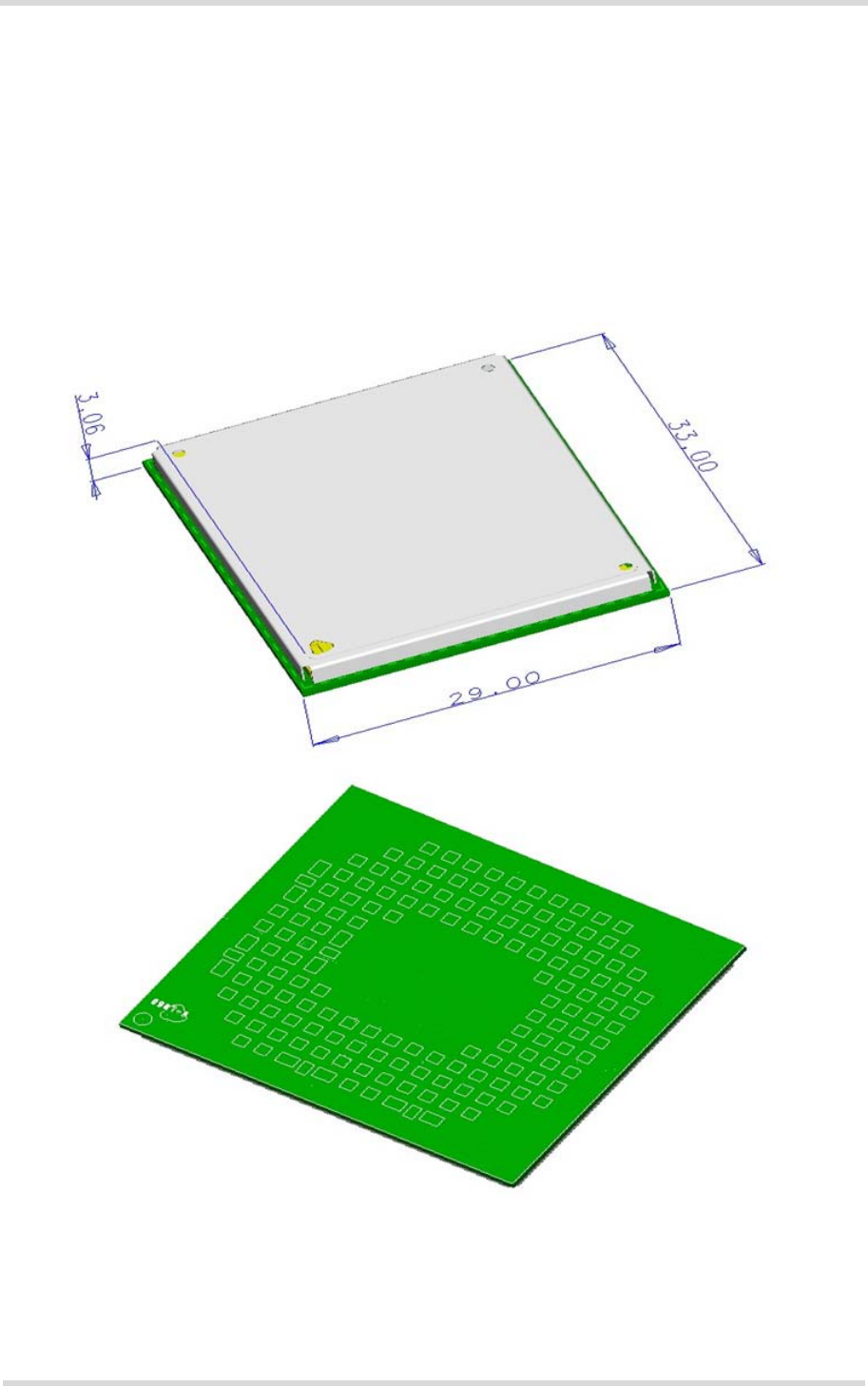
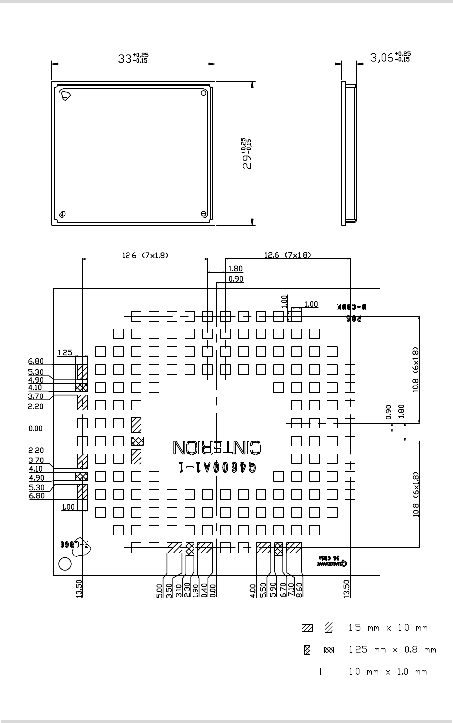
Physical Dimensions: 33mm x 29mm x 3.06mm
Weight: approx. 5g
RoHS All hardware components fully compliant with EU RoHS Directive
LTE features
3GPP Release 9 UE CAT 1 supported
DL 10.2Mbps, UL 5.2Mbps
HSPA features
3GPP Release 8 DL 7.2Mbps, UL 5.7Mbps
HSDPA Cat.8 / HSUPA Cat.6 data rates
Compressed mode (CM) supported according to 3GPP TS25.212
UMTS features
3GPP Release 4 PS data rate – 384 kbps DL / 384 kbps UL
CS data rate – 64 kbps DL / 64 kbps UL
GSM/GPRS/EGPRS features
Data transfer GPRS:
• Multislot Class 12
• Full PBCCH support
• Mobile Station Class B
• Coding Scheme 1 – 4
EGPRS:
• Multislot Class 12
• EDGE E2 power class for 8 PSK
• Downlink coding schemes – CS 1-4, MCS 1-9
• Uplink coding schemes – CS 1-4, MCS 1-9
• SRB loopback and test mode B
• 8-bit, 11-bit RACH
• PBCCH support
• 1 phase/2 phase access procedures
• Link adaptation and IR
• NACC, extended UL TBF
• Mobile Station Class B
SMS Point-to-point MT and MO
Cell broadcast
Text and PDU mode
Storage: SIM card plus SMS locations in mobile equipment
Software
AT commands Hayes 3GPP TS 27.007, TS 27.005, Gemalto M2M
AT commands for RIL compatibility
Feature Implementation

Cinterion® PLS62-W Hardware Interface Overview
1.1 Key Features at a Glance
11
PLS62-W_hio_v00.080 2017-10-12
Confidential / Preliminary
Page 9 of 46
Java™ Open Platform Java™ Open Platform with
• Java™ profile IMP-NG & CLDC 1.1 HI
• Secure data transmission via HTTPS/SSL1
• Multi-threading programming and multi-application execution
Major benefits: seamless integration into Java applications, ease of pro-
gramming, no need for application microcontroller, extremely cost-efficient
hardware and software design – ideal platform for industrial applications.
The memory space available for Java programs is 30MB in the flash file
system and 18MB RAM. Application code and data share the space in the
flash file system and in RAM.
Microsoft™ compatibility RIL for Pocket PC and Smartphone
SIM Application Toolkit SAT letter classes b, c, e; with BIP
Firmware update Generic update from host application over ASC0 or USB modem.
Interfaces
Module interface Surface mount device with solderable connection pads (SMT application
interface). Land grid array (LGA) technology ensures high solder joint reli-
ability and allows the use of an optional module mounting socket.
For more information on how to integrate SMT modules see also [3]. This
application note comprises chapters on module mounting and application
layout issues as well as on additional SMT application development equip-
ment.
USB USB 2.0 High Speed (480Mbit/s) device interface, Full Speed (12Mbit/s)
compliant
2 serial interfaces ASC0 (in parts shared with GPIO lines):
• 8-wire modem interface with status and control lines, unbalanced, asyn-
chronous
• Adjustable baud rates: 1,200bps to 921,600bps
• Autobauding: 1,200bps to 230,400bps
• Supports RTS0/CTS0 hardware flow control.
ASC1 (shared with GPIO lines):
• 4-wire, unbalanced asynchronous interface
• Adjustable baud rates: 1,200bps to 921,600bps
• Autobauding: 1,200bps to 230,400bps
• Supports RTS1/CTS1 hardware flow control
UICC interface Supported SIM/USIM cards: 3V, 1.8V
GPIO interface 24 GPIO lines comprising:
14 lines shared with ASC0, ASC1 and SPI lines, with network status indica-
tion, PWM functionality, fast shutdown, pulse counter, and SIM switch
10 GPIO lines not shared
I2C interface Supports I2C serial interface
SPI interface Serial peripheral interface, shared with GPIO lines
Antenna switch interface Control signal for 700MHz antenna switch
TX activity interface Signal indicating 2G/3G/4G transmit activities
Antenna interface pads 50Ω. UMTS/GSM/LTE main antenna, UMTS/LTE Rx Diversity antenna
Feature Implementation

Cinterion® PLS62-W Hardware Interface Overview
1.1 Key Features at a Glance
11
PLS62-W_hio_v00.080 2017-10-12
Confidential / Preliminary
Page 10 of 46
Power on/off, Reset
Power on/off Switch on by hardware signal IGT
Switch off by AT command
Switch off by emergency off signal (EMERG_OFF)
Switch off by hardware signal FST_SHDN instead of AT command
Automatic switch off in case of critical temperature or voltage conditions
Reset Orderly shutdown and reset by AT command
Special features
Real time clock Timer functions via AT commands
Evaluation kit
Evaluation module PLS62-W module soldered onto a dedicated PCB that can be connected to
an adapter in order to be mounted onto the DSB75.
DSB75 DSB75 Development Support Board designed to test and type approve
Gemalto M2M modules and provide a sample configuration for application
engineering. A special adapter is required to connect the PLS62-W evalu-
ation module to the DSB75.
1. HTTP/SecureConnection over SSL version 3.0 and TLS versions 1.0, 1.1, and 1.2 are supported. For
details please refer to Java User’s Guide for Cinterion® PLS62-W.
Feature Implementation
Cinterion® PLS62-W Hardware Interface Overview
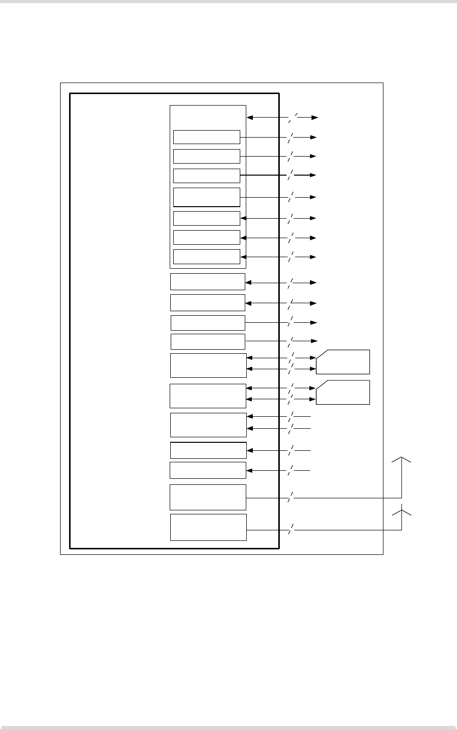
1.2 PLS62-W System Overview
11
PLS62-W_hio_v00.080 2017-10-12
Confidential / Preliminary
Page 11 of 46
1.2 PLS62-W System Overview
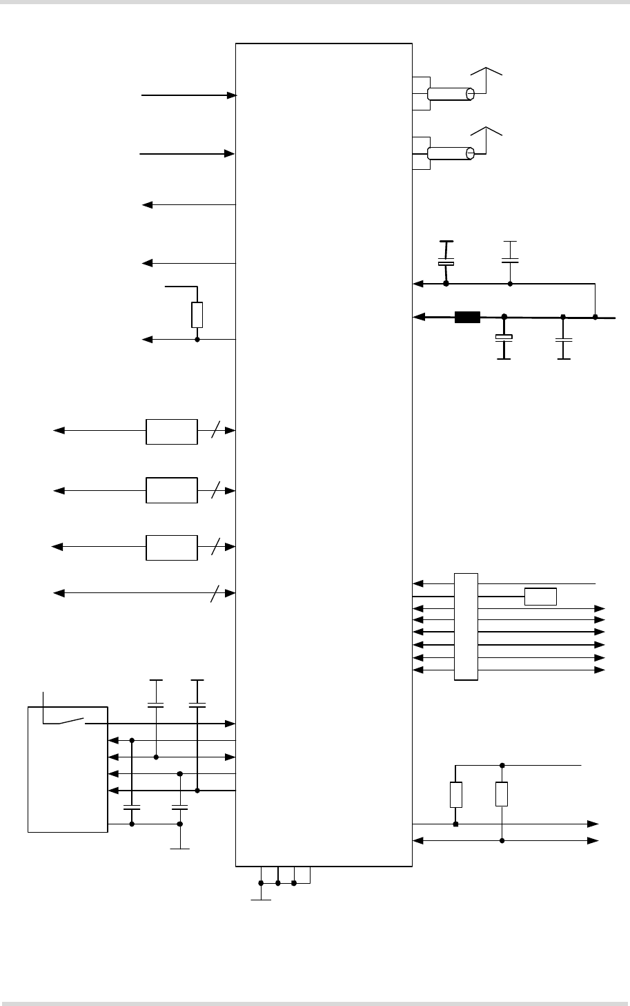
Figure 1: PLS62-W system overview
GPIO
interface
TX_ACTIVITY
ANT_SWITCH
I2C
CONTROL
RTC
POWER
Rx diversity
antenna
(UMTS/LTE)
Module
SIM Interface 1
(with SIM detection)
SIM card 1
Application
Power supply
Backup supply
Emergency off
IGT
I2C
USB
GPIO
2
2
5
10
1
1
1
1
TX activity
Antenna switch
Rx diversity
1
Status LED
1
DAC (PWM) PWM
2
Fast shutdown Fast shutdown
1
1
COUNTER Pulse counter
1
Main antenna
(GSM/UMTS/LTE)
Main antenna
1
SIM Interface 2
(with SIM detection)
SIM card 2
51
ASC1/SPI ASC1/SPI lines
4
ASC0/SPI ASC0/SPI line
4
USB
3
SIM_SWITCH SIM_SWITCH
1
ASC0 ASC0 lines
4
Cinterion® PLS62-W Hardware Interface Overview
2 Interface Characteristics
28
PLS62-W_hio_v00.080 2017-10-12
Confidential / Preliminary
Page 12 of 46
2 Interface Characteristics
PLS62-W is equipped with an SMT application interface that connects to the external applica-
tion. The SMT application interface incorporates the various application interfaces as well as
the RF antenna interface.
2.1 Application Interface
2.1.1 USB Interface
PLS62-W supports a USB 2.0 High Speed (480Mbit/s) device interface that is Full Speed
(12Mbit/s) compliant. The USB interface is primarily intended for use as command and data
interface and for downloading firmware.
The external application is responsible for supplying the VUSB_IN line. This line is used for ca-
ble detection only. The USB part (driver and transceiver) is supplied by means of BATT+. This
is because PLS62-W is designed as a self-powered device compliant with the “Universal Serial
Bus Specification Revision 2.0”1.
Figure 2: USB circuit
To properly connect the module's USB interface to the external application, a USB 2.0 compat-
ible connector and cable or hardware design is required. Furthermore, the USB modem driver
distributed with PLS62-W needs to be installed.
1. The specification is ready for download on http://www.usb.org/developers/docs/
VBUS
DP
DN
VREG (3V075)
BATT+
USB_DP2)
lin. reg.
GND
Module
Detection only VUSB_IN
USB part1)
RING0
Host wakeup
1) All serial (including R
S) and pull-up resistors for data lines are implemented.
USB_DN2)
2) If the USB interface is operated in High Speed mode (480MHz), it is recommended to take
special care routing the data lines USB_DP and USB_DN. Application layout should in this
case implement a differential impedance of 90Ohm for proper signal integrity.
RS
RS
SMT
Cinterion® PLS62-W Hardware Interface Overview
2.1 Application Interface
28
PLS62-W_hio_v00.080 2017-10-12
Confidential / Preliminary
Page 13 of 46
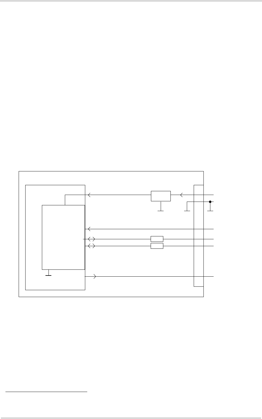
2.1.2 Serial Interface ASC0
PLS62-W offers an 8-wire unbalanced, asynchronous modem interface ASC0 conforming to
ITU-T V.24 protocol DCE signalling. The electrical characteristics do not comply with ITU-T
V.28. The significant levels are 0V (for low data bit or active state) and 1.8V (for high data bit
or inactive state).
PLS62-W is designed for use as a DCE. Based on the conventions for DCE-DTE connections
it communicates with the customer application (DTE) using the following signals:
• Port TXD @ application sends data to the module’s TXD0 signal line
• Port RXD @ application receives data from the module’s RXD0 signal line
Figure 3: Serial interface ASC0
Features:
• Includes the data lines TXD0 and RXD0, the status lines RTS0 and CTS0 and, in addition,
the modem control lines DTR0, DSR0, DCD0 and RING0.
• The RING0 signal serves to indicate incoming calls and other types of URCs (Unsolicited
Result Code). It can also be used to send pulses to the host application, for example to
wake up the application from power saving state.
• Configured for 8 data bits, no parity and 1 stop bit.
• ASC0 can be operated at fixed bit rates from 1,200bps up to 921,600bps.
• Autobauding supports bit rates from 1,200bps up to 230,400bps.
• Supports RTS0/CTS0 hardware flow control. The hardware hand shake line RTS0 has an
internal pull down resistor causing a low level signal, if the line is not used and open.
Although hardware flow control is recommended, this allows communication by using only
RXD and TXD lines.
• Wake up from SLEEP mode by RTS0 activation.
Cinterion® PLS62-W Hardware Interface Overview
2.1 Application Interface
28
PLS62-W_hio_v00.080 2017-10-12
Confidential / Preliminary
Page 14 of 46
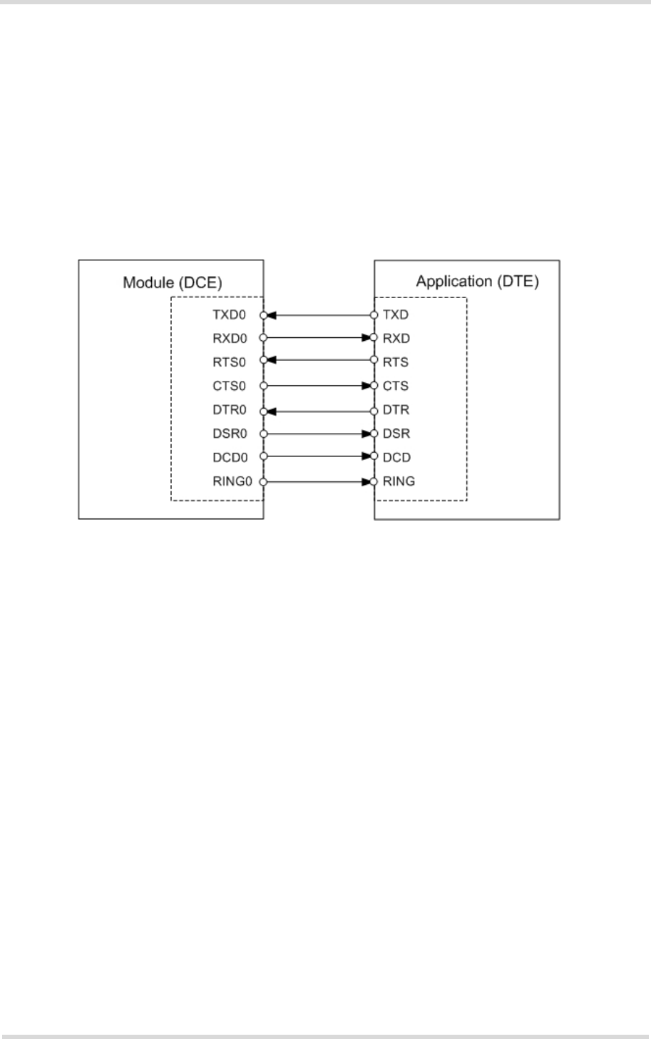
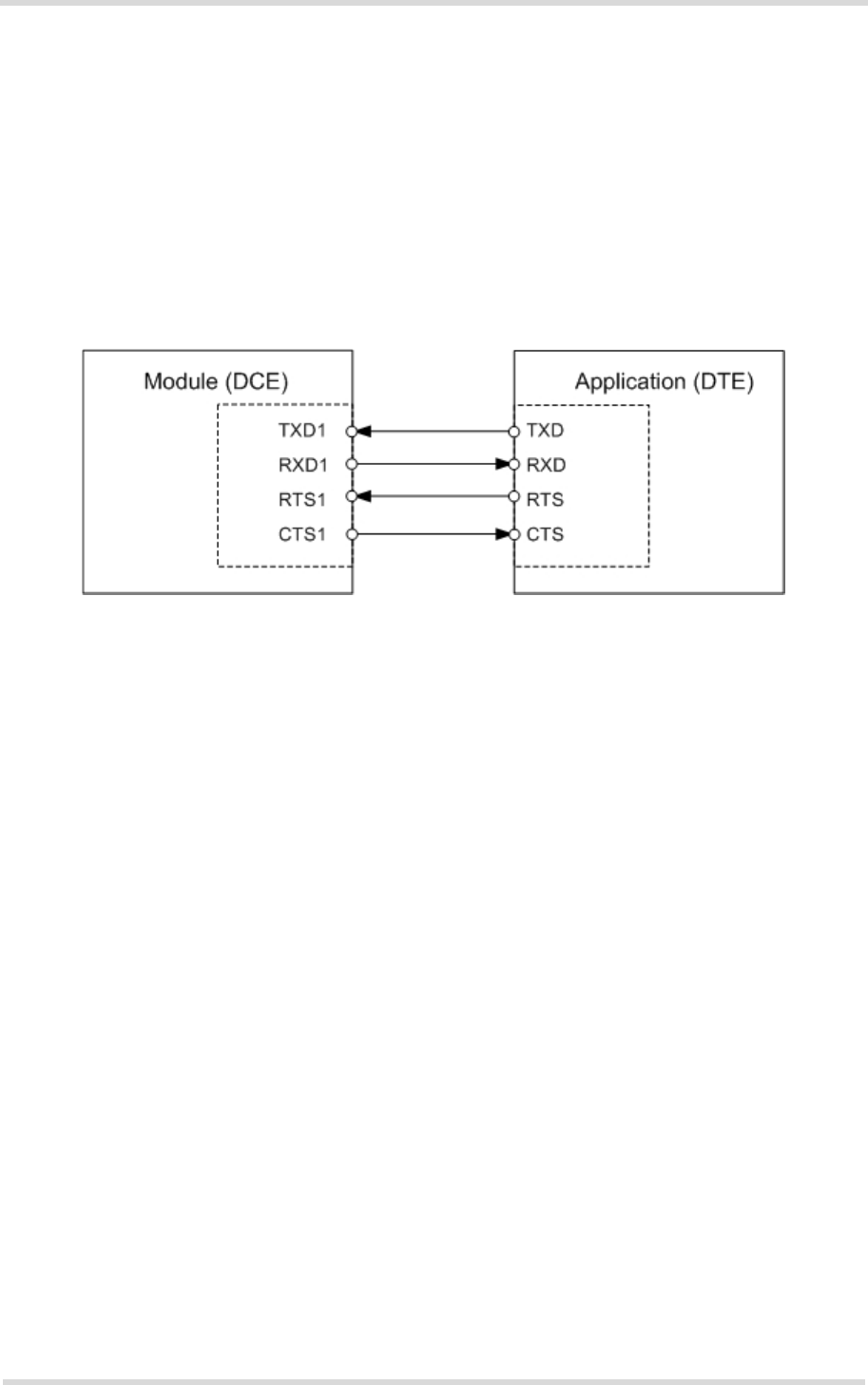
2.1.3 Serial Interface ASC1
Four PLS62-W GPIO lines can be configured as ASC1 interface signals to provide a 4-wire un-
balanced, asynchronous modem interface ASC1 conforming to ITU-T V.24 protocol DCE sig-
nalling. The electrical characteristics do not comply with ITU-T V.28. The significant levels are
0V (for low data bit or active state) and 1.8V (for high data bit or inactive state).
PLS62-W is designed for use as a DCE. Based on the conventions for DCE-DTE connections
it communicates with the customer application (DTE) using the following signals:
• Port TXD @ application sends data to module’s TXD1 signal line
• Port RXD @ application receives data from the module’s RXD1 signal line
Figure 4: Serial interface ASC1
Features
• Includes only the data lines TXD1 and RXD1 plus RTS1 and CTS1 for hardware hand-
shake.
• On ASC1 no RING line is available.
• Configured for 8 data bits, no parity and 1 or 2 stop bits.
• ASC1 can be operated at fixed bit rates from 1,200 bps to 921,600 bps.
• Autobauding supports bit rates from 1,200bps up to 230,400bps.
• Supports RTS1/CTS1 hardware flow. The hardware hand shake line RTS0 has an internal
pull down resistor causing a low level signal, if the line is not used and open. Although hard-
ware flow control is recommended, this allows communication by using only RXD and TXD
lines.

Cinterion® PLS62-W Hardware Interface Overview
2.1 Application Interface
28
PLS62-W_hio_v00.080 2017-10-12
Confidential / Preliminary
Page 15 of 46
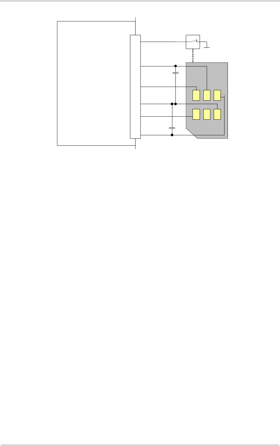
2.1.4 UICC/SIM/USIM Interface
PLS62-W has two UICC/SIM/USIM interfaces compatible with the 3GPP 31.102 and ETSI 102
221. These are wired to the host interface in order to be connected to an external SIM card
holder. Five pads on the SMT application interface are reserved for each of the two SIM inter-
faces.
The UICC/SIM/USIM interface supports 3V and 1.8V SIM cards.
The CCINx signal serves to detect whether a tray (with SIM card) is present in the card holder.
Using the CCINx signal is mandatory for compliance with the GSM 11.11 recommendation if
the mechanical design of the host application allows the user to remove the SIM card during
operation. To take advantage of this feature, an appropriate SIM card detect switch is required
on the card holder. For example, this is true for the model supplied by Molex, which has been
tested to operate with PLS62-W and is part of the Gemalto M2M reference equipment submit-
ted for type approval. See Chapter 7 for Molex ordering numbers.
Note: No guarantee can be given, nor any liability accepted, if loss of data is encountered after
removing the SIM card during operation. Also, no guarantee can be given for properly initializ-
ing any SIM card that the user inserts after having removed the SIM card during operation. In
this case, the application must restart PLS62-W.
By default, only the module’s 1st SIM interface is available and can be used. Using
SIM_SWITCH line it is possible to switch between the two SIM interfaces (see Section 2.1.4.1).
Table 1: Signals of the SIM interface (SMT application interface)
Signal Description
GND Ground connection for SIM interfaces. Optionally a separate SIM ground line using e.g.,
pad P12, may be used to improve EMC.
CCCLK1
CCCLK2
Chipcard clock lines for 1st and 2nd SIM interface.
CCVCC1
CCVCC2
SIM supply voltage lines for 1st and 2nd SIM interface.
CCIO1
CCIO2
Serial data lines for 1st and 2nd SIM interface, input and output.
CCRST1
CCRST2
Chipcard reset lines for 1st and 2nd SIM interface.
CCIN1
CCIN2
Input on the baseband processor for detecting a SIM card tray in the holder. If the SIM is
removed during operation the SIM interface is shut down immediately to prevent destruc-
tion of the SIM. The CCINx signal is active low.
The CCINx signal is mandatory for applications that allow the user to remove the SIM card
during operation.
The CCINx signal is solely intended for use with a SIM card. It must not be used for any
other purposes. Failure to comply with this requirement may invalidate the type approval of
PLS62-W.
Cinterion® PLS62-W Hardware Interface Overview
2.1 Application Interface
28
PLS62-W_hio_v00.080 2017-10-12
Confidential / Preliminary
Page 16 of 46
Figure 5: UICC/SIM/USIM interfaces
The total cable length between the SMT application interface pads on PLS62-W and the pads
of the external SIM card holder must not exceed 100mm in order to meet the specifications of
3GPP TS 51.010-1 and to satisfy the requirements of EMC compliance.
To avoid possible cross-talk from the CCCLKx signal to the CCIOx signal be careful that both
lines are not placed closely next to each other. A useful approach is using the GND line to
shield the CCIOx line from the CCCLKx line.
2.1.4.1 SIM Card Interface Switch
Using the SIM_SWITCH line allows to switch between two SIM card interfaces. The usage of
both interfaces is mutually exclusive. The GPIO26 line can be configured as SIM_SWITCH by
means of AT-Command. If set to low, the 1st SIM card interface will be used, if set to high the
2nd SIM card interface will be used.
The configuration of the SIM_SWITCH line is done via AT command, is non-volatile, and avail-
able after the next module restart.
Module
open: Card removed
closed: Card inserted
CCRSTx
CCVCCx
CCIOx
CCCLKx
CCINx
SIM /
UICC
1n
220n
SMT application interface
GND

Cinterion® PLS62-W Hardware Interface Overview
2.1 Application Interface
28
PLS62-W_hio_v00.080 2017-10-12
Confidential / Preliminary
Page 17 of 46
2.1.5 GPIO Interface
PLS62-W offers a GPIO interface with 24 GPIO lines. The GPIO lines are shared with other
interfaces or functions: Fast shutdown (see Section 2.1.10.1), status LED (see Section 2.1.10),
the PWM functionality (see Section 2.1.8), an pulse counter (see Section 2.1.9), ASC0 (see
Section 2.1.2), ASC1 (see Section 2.1.3), an SPI interface (see Section 2.1.7).
The following table shows the configuration variants for the GPIO pads. All variants are mutu-
ally exclusive, i.e. a pad configured for instance as Status LED is locked for alternative usage.
After startup, the above mentioned alternative GPIO line assignments can be configured using
AT commands (see [1]). The configuration is non-volatile and available after module restart.
Table 2: GPIO lines and possible alternative assignment
GPIO Fast
Shutdown Status
LED PWM Pulse
Counter ASC0 ASC1 SPI SIM
SWITCH
GPIO1 DTR0
GPIO2 DCD0
GPIO3 DSR0 SPI_CLK
GPIO4 FST_SHDN
GPIO5 Status LED
GPIO6 PWM2
GPIO7 PWM1
GPIO8 COUNTER
GPIO11
GPIO12
GPIO13
GPIO14
GPIO15
GPIO16 RXD1 SPI_MOSI
GPIO17 TXD1 SPI_MISO
GPIO18 RTS1
GPIO19 CTS1 SPI_CS
GPIO20
GPIO21
GPIO22
GPIO23
GPIO24 RING0
GPIO25
GPIO26 SIM_SWITCH

Cinterion® PLS62-W Hardware Interface Overview
2.1 Application Interface
28
PLS62-W_hio_v00.080 2017-10-12
Confidential / Preliminary
Page 18 of 46
2.1.6 I2C Interface
I2C is a serial, 8-bit oriented data transfer bus for bit rates up to 400kbps in Fast mode. It con-
sists of two lines, the serial data line I2CDAT and the serial clock line I2CCLK. The module acts
as a single master device, e.g. the clock I2CCLK is driven by the module. I2CDAT is a bi-direc-
tional line. Each device connected to the bus is software addressable by a unique 7-bit ad-
dress, and simple master/slave relationships exist at all times. The module operates as master-
transmitter or as master-receiver. The customer application transmits or receives data only on
request of the module.
The I2C interface can be powered via the V180 line of PLS62-W. If connected to the V180 line,
the I2C interface will properly shut down when the module enters the Power Down mode.
Note: Good care should be taken when creating the PCB layout of the host application: The
traces of I2CCLK and I2CDAT should be equal in length and as short as possible.
2.1.7 SPI Interface
Four PLS62-W GPIO interface lines can be configured as Serial Peripheral Interface (SPI). The
SPI is a synchronous serial interface for control and data transfer between PLS62-W and the
external application. Only one application can be connected to the SPI and the interface sup-
ports only master mode. The transmission rates are up to 6.5Mbit/s. The SPI interface compris-
es the two data lines SPI_MOSI and SPI_MISO, the clock line SPI_CLK a well as the chip
select line SPI_CS.
2.1.8 PWM Interfaces
The GPIO6 and GPIO7 interface lines can be configured as Pulse Width Modulation interface
lines PWM1 and PWM2. The PWM interface lines can be used, for example, to connect buzz-
ers. The PWM1 line is shared with GPIO7 and the PWM2 line is shared with GPIO6 (for GPIOs
see Section 2.1.5). GPIO and PWM functionality are mutually exclusive.
2.1.9 Pulse Counter
The GPIO8 line can be configured as pulse counter line COUNTER. The pulse counter inter-
face can be used, for example, as a clock (for GPIOs see Section 2.1.5).
2.1.10 Status LED
The GPIO5 interface line can be configured to drive a status LED that indicates different oper-
ating modes of the module (for GPIOs see Section 2.1.5). GPIO and LED functionality are mu-
tually exclusive.

Cinterion® PLS62-W Hardware Interface Overview
2.1 Application Interface
28
PLS62-W_hio_v00.080 2017-10-12
Confidential / Preliminary
Page 19 of 46
2.1.10.1 Fast Shutdown
The GPIO4 interface line can be configured as fast shutdown signal line FST_SHDN. The con-
figured FST_SHDN line is an active low control signal and must be applied for at least 1 milli-
seconds. If unused this line can be left open because of a configured internal pull-up resistor.
2.1.11 700MHz Antenna Switch Control
To provide for an antenna optimization over a wide frequency range, the ANT_SWITCH line
may act as a control signal for a possible external antenna switch that is able to change
between an antenna covering the 700MHz band and an antenna covering all other bands -
depending on the frequency band currently being used by the module.
The ANT_SWITCH line is set to "high" (1) if the module is employing frequencies in the 700
MHz range (i.e., LTE band 17) and "low" (0) for all other frequencies, including the 800/850
MHz frequency bands.
The ANT_SWITCH signal is triggered by all module internal activities involving a change of the
used frequency, even if only temporary (e.g., inter-band scanning using compressed mode).
The maximum delay/deviation between internal usage change of the frequency band, and the
GPIO2 signal change is 10 microseconds.
2.1.12 TX Activity Signal
The TX_ACTIVITY line indicates any 2G/3G/4G TX activity of the module, meaning a high level
on this line signals that the module is transmitting data.

Cinterion® PLS62-W Hardware Interface Overview
2.2 RF Antenna Interface
28
PLS62-W_hio_v00.080 2017-10-12
Confidential / Preliminary
Page 20 of 46
2.2 RF Antenna Interface
The PLS62-W GSM/UMTS/LTE antenna interface comprises a GSM/UMTS/LTE main antenna
as well as a UMTS/LTE Rx diversity antenna to improve signal reliability and quality1. The RF
interface has an impedance of 50Ω. PLS62-W is capable of sustaining a total mismatch at the
antenna line without any damage, even when transmitting at maximum RF power.
The external antenna must be matched properly to achieve best performance regarding radi-
ated power, modulation accuracy and harmonic suppression. Antenna matching networks are
not included on the PLS62-W module and should be placed in the host application if the anten-
na does not have an impedance of 50Ω.
Regarding the return loss PLS62-W provides the following values in the active band:
1. By delivery default the UMTS/LTE Rx diversity antenna is configured as available for the module since
its usage is mandatory for LTE. Please refer to [1] for details on how to configure antenna settings.
Table 3: Return loss in the active band
State of module Return loss of module Recommended return loss of application
Receive > 8dB > 12dB
Transmit not applicable > 12dB
Cinterion® PLS62-W Hardware Interface Overview
2.2 RF Antenna Interface
28
PLS62-W_hio_v00.080 2017-10-12
Confidential / Preliminary
Page 21 of 46
2.2.1 Antenna Installation
The antenna is connected by soldering the antenna pads (ANT_MAIN and ANT_DRX) and
their neighboring ground pads directly to the application’s PCB.
The distance between the antenna pads and their neighboring GND pads has been optimized
for best possible impedance. To prevent mismatch, special attention should be paid to these
pads on the application’ PCB.
The wiring of the antenna connection, starting from the antenna pad to the application’s anten-
na should result in a 50 line impedance. Line width and distance to the GND plane need to
be optimized with regard to the PCB’s layer stack.
To prevent receiver desensitization due to interferences generated by fast transients like high
speed clocks on the external application PCB, it is recommended to realize the antenna con-
nection line using embedded Stripline rather than Micro-Stripline technology.
For type approval purposes, the use of a 50 coaxial antenna connector (U.FL-R-SMT) might
be necessary. In this case the U.FL-R-SMT connector should be placed as close as possible
to PLS62-W‘s antenna pad.
2.2.2 RF Line Routing Design
2.2.2.1 Line Arrangement Examples
Several dedicated tools are available to calculate line arrangements for specific applications
and PCB materials - for example from http://www.polarinstruments.com/ (commercial software)
or from http://web.awrcorp.com/Usa/Products/Optional-Products/TX-Line/ (free software).
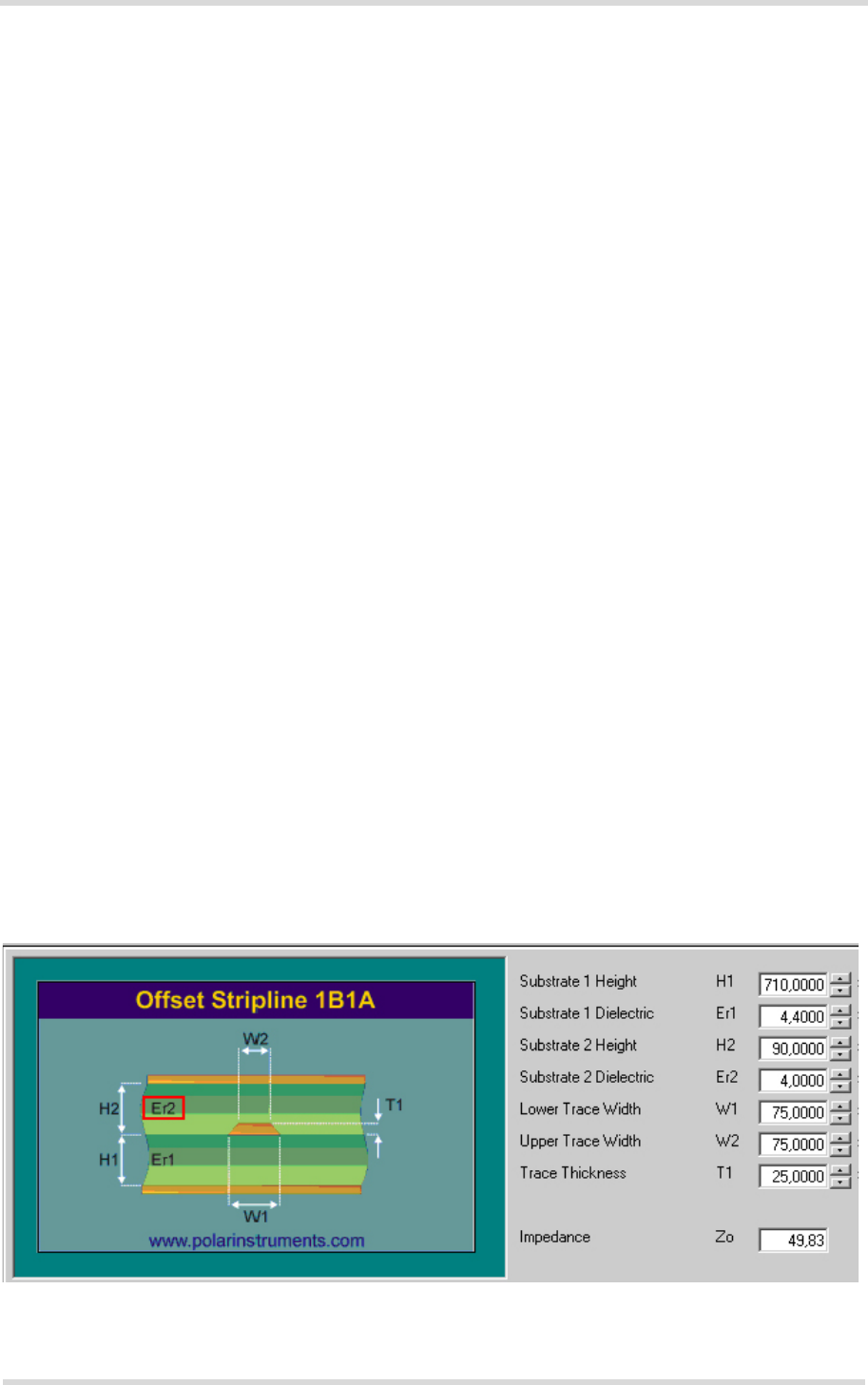
Embedded Stripline
This figure below shows a line arrangement example for embedded stripline with 65µm FR4
prepreg (type: 1080) and 710µm FR4 core (4-layer PCB).
Figure 6: Embedded Stripline with 65µm prepreg (1080) and 710µm core
Cinterion® PLS62-W Hardware Interface Overview
2.2 RF Antenna Interface
28
PLS62-W_hio_v00.080 2017-10-12
Confidential / Preliminary
Page 22 of 46
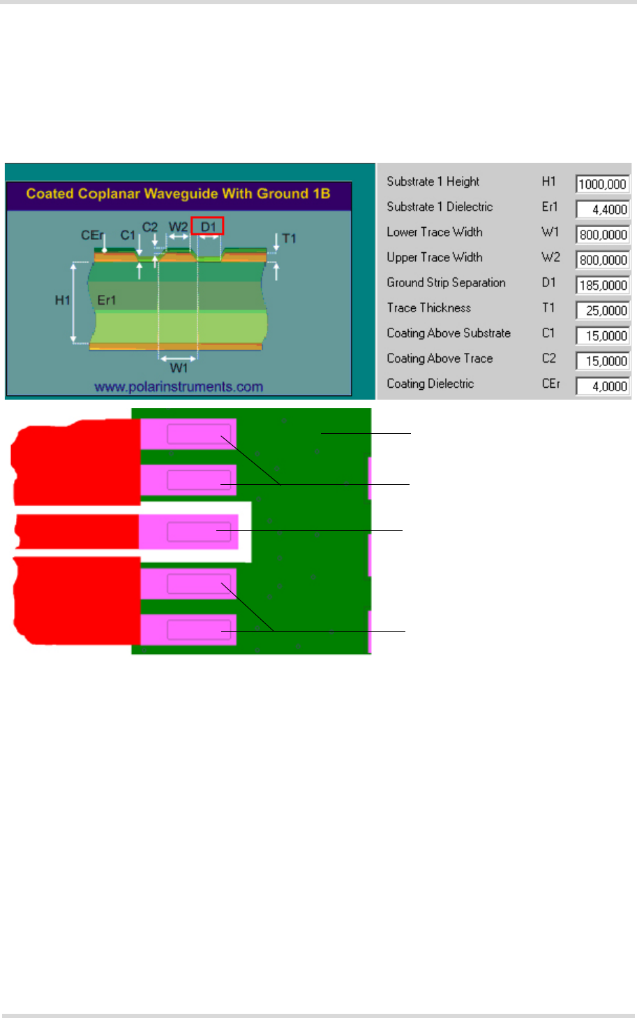
Micro-Stripline
This section gives two line arrangement examples for micro-stripline.
• Micro-Stripline on 1.0mm Standard FR4 2-Layer PCB
The following two figures show examples with different values for D1 (ground strip separa-
tion).
Figure 7: Micro-Stripline on 1.0mm standard FR4 2-layer PCB - example 1
Antenna line
Ground line
Ground line
Application board
Cinterion® PLS62-W Hardware Interface Overview
2.2 RF Antenna Interface
28
PLS62-W_hio_v00.080 2017-10-12
Confidential / Preliminary
Page 24 of 46
• Micro-Stripline on 1.5mm Standard FR4 2-Layer PCB
The following two figures show examples with different values for D1 (ground strip separa-
tion).
Figure 9: Micro-Stripline on 1.5mm Standard FR4 PCB - example 1
Antenna line
Ground line
Ground line
Application board
Cinterion® PLS62-W Hardware Interface Overview
2.2 RF Antenna Interface
28
PLS62-W_hio_v00.080 2017-10-12
Confidential / Preliminary
Page 26 of 46
2.2.2.2 Routing Example
Interface to RF Connector
Figure 11 shows a sample connection of a module‘s antenna pad at the bottom layer of the
module PCB with an application PCB‘s coaxial antenna connector. Line impedance depends
on line width, but also on other PCB characteristics like dielectric, height and layer gap. The
sample stripline width of 0.33mm is recommended for an application with a PCB layer stack
resembling the one of the PLS62-W evaluation board shown in Figure 12. For different layer
stacks the stripline width will have to be adapted accordingly.
Figure 11: Routing to application‘s RF connector
Figure 12: PLS62-W evaluation board layer table
e.g.
ANT_
MAIN
G N D G N D
Edge of module PCB
Stripline (50 ohms) on top
layer of evaluation board from
antenna pad to module edge
Width = 0.33 mm
E.g., U.FL antenna
connector
50 ohms microstrip line
G N D G N D
Ground connection

Cinterion® PLS62-W Hardware Interface Overview
2.3 Sample Application
28
PLS62-W_hio_v00.080 2017-10-12
Confidential / Preliminary
Page 27 of 46
2.3 Sample Application
Figure 13 shows a typical example of how to integrate a PLS62-W module with an application.
Usage of the various host interfaces depends on the desired features of the application.
Because of the very low power consumption design, current flowing from any other source into
the module circuit must be avoided, for example reverse current from high state external control
lines. Therefore, the controlling application must be designed to prevent reverse current flow.
Otherwise there is the risk of undefined states of the module during startup and shutdown or
even of damaging the module.
Because of the high RF field density inside the module, it cannot be guaranteed that no self
interference might occur, depending on frequency and the applications grounding concept. The
potential interferers may be minimized by placing small capacitors (47pF) at suspected lines
(e.g. RXD0, VDDLP, and ON).
While developing SMT applications it is strongly recommended to provide test points
for certain signals, i.e., lines to and from the module - for debug and/or test purposes.
The SMT application should allow for an easy access to these signals. For details on
how to implement test points see [3].
The EMC measures are best practice recommendations. In fact, an adequate EMC strategy for
an individual application is very much determined by the overall layout and, especially, the po-
sition of components.
Note: PLS62-W is not intended for use with cables longer than 3m.
Disclaimer
No warranty, either stated or implied, is provided on the sample schematic diagram shown in
Figure 13 and the information detailed in this section. As functionality and compliance with na-
tional regulations depend to a great amount on the used electronic components and the indi-
vidual application layout manufacturers are required to ensure adequate design and operating
safeguards for their products using PLS62-W modules.
Cinterion® PLS62-W Hardware Interface Overview
2.3 Sample Application
28
PLS62-W_hio_v00.080 2017-10-12
Confidential / Preliminary
Page 28 of 46
Figure 13: Schematic diagram of PLS62-W sample application
PWR_IND
V180
ASC0 (including GPIO1...GPIO3 for
DSR0, DTR0, DCD0 and GPIO24 for
RING0)/ SPI_CLK (for DSR0)
GPIO16...GPIO19/
ASC1/
SPI
8
4
CCVCCx
CCIOx
CCCLKx
CCINx
CCRSTx
SIM
V180
220nF 1nF
I2CCLK
I2CDAT
2.2k***
V180
GPIO4 (FST_SHDN)
GPIO5 (STATUS)
GPIO6 (PWM2)
GPIO7 (PWM1)
GPIO8 (COUNTER)
GPIO11...GPIO15
GPIO25
GPIO26
(SIM_SWITCH)
LED
GND
GND
GND
ANT_MAIN
BATT+RF
Power suppl
y
Main antenna
PLS62
All SIM components should be
close to card holder. Keep SIM
wires low capacitive.
*10pF *10pF
* Add optional 10pF for SIM protection
against RF (internal Antenna)
150µF,
Low ESR! 33pF
Bl ocki ng **
Blocking**
Blocking**
PWR_IND
BATT+BB
53
204
GPIO20...GPIO23
4
Blocking**
2.2k***
3USB
150µF,
Low ESR!
33pF
GND
GND
ANT_DRX
Diversity antenna
EMERG_OFF
IGT
BEAD*
BEAD*: It is recommended to add the
BEAD as shown to the BATT+BB line. The
purpose of this is to mitigate noise from
baseband power supply.
Note 1: BLM15PD121SN1D MURATA Ind
Chip Bead (120Ohm 25% 100MHz Ferrite
1.3A) is recommended in this case. For
details please visit www.murata.com.
Note 2: The Bead should be placed as
close as possible to the module.
*** I2
C interface of the module already
has internal 1KOhm pull up resistor to
V180 inside the module. Please take
this into consideration during
application design.
EMERG_OFF
IGT
V180
VDDLP
VDDLP
E.g., 100k
E.g., VBATT

Cinterion® PLS62-W Hardware Interface Overview
3 Operating Characteristics
30
PLS62-W_hio_v00.080 2017-10-12
Confidential / Preliminary
Page 29 of 46
3 Operating Characteristics
3.1 Operating Modes
The table below briefly summarizes the various operating modes referred to throughout the
document.
Mode Function
Normal
operation
GSM /
GPRS / UMTS /
HSPA / LTE
SLEEP
Power saving set automatically when no call is in progress and the USB
connection is suspended by host or not present and no active commu-
nication via ASC0.
GSM /
GPRS / UMTS /
HSPA / LTE IDLE
Power saving disabled or an USB connection not suspended, but no
call in progress.
GSM TALK/
GSM DATA
Connection between two subscribers is in progress. Power consump-
tion depends on the GSM network coverage and several connection
settings (e.g. DTX off/on, FR/EFR/HR, hopping sequences and
antenna connection). The following applies when power is to be mea-
sured in TALK_GSM mode: DTX off, FR and no frequency hopping.
GPRS DATA GPRS data transfer in progress. Power consumption depends on net-
work settings (e.g. power control level), uplink / downlink data rates and
GPRS configuration (e.g. used multislot settings).
EGPRS DATA EGPRS data transfer in progress. Power consumption depends on net-
work settings (e.g. power control level), uplink / downlink data rates and
EGPRS configuration (e.g. used multislot settings).
UMTS TALK/
UMTS DATA
UMTS data transfer in progress. Power consumption depends on net-
work settings (e.g. TPC Pattern) and data transfer rate.
HSPA DATA HSPA data transfer in progress. Power consumption depends on net-
work settings (e.g. TPC Pattern) and data transfer rate.
LTE DATA LTE data transfer in progress. Power consumption depends on network
settings (e.g. TPC Pattern) and data transfer rate.
Power
Down
Normal shutdown after sending the power down command. Only a voltage regulator is
active for powering the RTC. Software is not active. Interfaces are not accessible. Operat-
ing voltage remains applied.
Airplane
mode
Airplane mode shuts down the radio part of the module, causes the module to log off from
the network and disables all AT commands whose execution requires a radio connection.
Airplane mode can be controlled by AT command (see [1]).

Cinterion® PLS62-W Hardware Interface Overview
3.2 Power Supply
30
PLS62-W_hio_v00.080 2017-10-12
Confidential / Preliminary
Page 30 of 46
3.2 Power Supply
PLS62-W needs to be connected to a power supply at the SMT application interface - 4 lines
BATT+, and GND. There are two separate voltage domains for BATT+:
•BATT+
BB with two lines for the general power management.
•BATT+
RF with four lines for the GSM power amplifier supply.
Please note that throughout the document BATT+ refers to both voltage domains and power
supply lines - BATT+BB and BATT+RF.
The main power supply from an external application has to be a single voltage source and has
to be expanded to sub paths (star structure).
All the key functions for supplying power to the device are handled by the power management
section of the analog controller. This IC provides the following features:
• Stabilizes the supply voltages for the baseband using low drop linear voltage regulators and
a DC-DC step down switching regulator.
• Switches the module's power voltages for the power-up and -down procedures.
• SIM switch to provide SIM power supply.
Cinterion® PLS62-W Hardware Interface Overview
4 Mechanical Dimensions, Mounting and Packaging
32
PLS62-W_hio_v00.080 2017-10-12
Confidential / Preliminary
Page 31 of 46
4 Mechanical Dimensions, Mounting and Packaging
4.1 Mechanical Dimensions of PLS62-W
Figure 14 shows the top and bottom view of PLS62-W and provides an overview of the board's
mechanical dimensions. For further details see Figure 15.
Figure 14: PLS62-W– top and bottom view
Top view
Bottom view
Cinterion® PLS62-W Hardware Interface Overview
5 Regulatory and Type Approval Information
39
PLS62-W_hio_v00.080 2017-10-12
Confidential / Preliminary
Page 33 of 46
5 Regulatory and Type Approval Information
5.1 Directives and Standards
PLS62-W is designed to comply with the directives and standards listed below.
It is the responsibility of the application manufacturer to ensure compliance of the final product
with all provisions of the applicable directives and standards as well as with the technical spec-
ifications provided in the "PLS62-W Hardware Interface Description”.1
1. Manufacturers of applications which can be used in the US shall ensure that their applications have a
PTCRB approval. For this purpose they can refer to the PTCRB approval of the respective module.
Table 4: Directives
2014/53/EU Directive of the European Parliament and of the council of 16 April 2014 on
the harmonization of the laws of the Member States relating to the making
available on the market of radio equipment and repealing Directive 1999/
05/EC.
The product is labeled with the CE conformity mark.
2002/95/EC (RoHS 1)
2011/65/EC (RoHS 2)
Directive of the European Parliament and of the Council of
27 January 2003 (and revised on 8 June 2011) on the
restriction of the use of certain hazardous substances in
electrical and electronic equipment (RoHS)
Table 5: Standards of North American type approval
CFR Title 47 Code of Federal Regulations, Part 22, Part 24; US Equipment Authorization
FCC
OET Bulletin 65
(Edition 97-01)
Evaluating Compliance with FCC Guidelines for Human Exposure to
Radiofrequency Electromagnetic Fields
UL 60 950-1 Product Safety Certification (Safety requirements)
NAPRD.03 V5.24 Overview of PCS Type certification review board Mobile Equipment Type
Certification and IMEI control
PCS Type Certification Review board (PTCRB)
RSS132, RSS133,
RSS139
Canadian Standard
Table 6: Standards of European type approval
3GPP TS 51.010-1 Digital cellular telecommunications system (Release 7); Mobile Station
(MS) conformance specification;
ETSI EN 301 511
V12.5.1
Global System for Mobile communications (GSM); Mobile Stations (MS)
equipment; Harmonized Standard covering the essential requirements of
article 3.2 of Directive 2014/53/EU
GCF-CC V3.62.1 Global Certification Forum - Certification Criteria
Cinterion® PLS62-W Hardware Interface Overview
5.1 Directives and Standards
39
PLS62-W_hio_v00.080 2017-10-12
Confidential / Preliminary
Page 34 of 46
Draft ETSI EN 301 489-
01 V2.2.0
Electromagnetic Compatibility (EMC) standard for radio equipment and ser-
vices; Part 1: Common technical requirements; Harmonized Standard cov-
ering the essential requirements of article 3.1(b) of Directive 2014/53/EU
and the essential requirements of article 6 of Directive 2014/30/EU
Draft ETSI EN 301 489-52
V1.1.0
Electromagnetic Compatibility (EMC) standard for radio equipment and ser-
vices; Part 52: Specific conditions for Cellular Communication Mobile and
portable (UE) radio and ancillary equipment; Harmonized Standard cover-
ing the essential requirements of article 3.1(b) of Directive 2014/53/EU
ETSI EN 301 908-01
V11.1.1
IMT cellular networks; Harmonized Standard covering the essential require-
ments of article 3.2 of the Directive 2014/53/EU; Part 1: Introduction and
common requirements
ETSI EN 301 908-02
V11.1.1
IMT cellular networks; Harmonized Standard covering the essential require-
ments of article 3.2 of the Directive 2014/53/EU; Part 2: CDMA Direct
Spread (UTRA FDD) User Equipment (UE)
ETSI EN 301 908-13
V11.1.1
IMT cellular networks; Harmonized Standard covering the essential require-
ments of article 3.2 of the Directive 2014/53/EU; Part 13: Evolved Universal
Terrestrial Radio Access (E-UTRA) User Equipment (UE)
EN 60950-1:2006/
A11:2009+A1:2010+A1
2:2011+A2:2013
Safety of information technology equipment
Table 7: Requirements of quality
IEC 60068 Environmental testing
DIN EN 60529 IP codes
Table 8: Standards of the Ministry of Information Industry of the People’s Republic of China
SJ/T 11363-2006 “Requirements for Concentration Limits for Certain Hazardous Sub-
stances in Electronic Information Products” (2006-06).
SJ/T 11364-2006 “Marking for Control of Pollution Caused by Electronic
Information Products” (2006-06).
According to the “Chinese Administration on the Control
of Pollution caused by Electronic Information Products”
(ACPEIP) the EPUP, i.e., Environmental Protection Use
Period, of this product is 20 years as per the symbol
shown here, unless otherwise marked. The EPUP is valid only as long as
the product is operated within the operating limits described in the
Gemalto M2M Hardware Interface Description.
Please see Table 9 for an overview of toxic or hazardous substances or
elements that might be contained in product parts in concentrations
above the limits defined by SJ/T 11363-2006.
Table 6: Standards of European type approval

Cinterion® PLS62-W Hardware Interface Overview
5.2 SAR requirements specific to portable mobiles
39
PLS62-W_hio_v00.080 2017-10-12
Confidential / Preliminary
Page 36 of 46
5.2 SAR requirements specific to portable mobiles
Mobile phones, PDAs or other portable transmitters and receivers incorporating a GSM/UMTS
module must be in accordance with the guidelines for human exposure to radio frequency en-
ergy. This requires the Specific Absorption Rate (SAR) of portable PLS62-W based applica-
tions to be evaluated and approved for compliance with national and/or international
regulations.
Since the SAR value varies significantly with the individual product design manufacturers are
advised to submit their product for approval if designed for portable use. For European/US/Aus-
tralian-markets the relevant directives are mentioned below. It is the responsibility of the man-
ufacturer of the final product to verify whether or not further standards, recommendations or
directives are in force outside these areas.
Products intended for sale on US markets
ES 59005/ANSI C95.1 Considerations for evaluation of human exposure to Electromagnetic
Fields (EMFs) from Mobile Telecommunication Equipment (MTE) in the
frequency range 30MHz - 6GHz
Products intended for sale on European markets
EN 50360 Product standard to demonstrate the compliance of mobile phones with
the basic restrictions related to human exposure to electromagnetic
fields (300MHz - 3GHz)
EN 62311:2008 Assessment of electronic and electrical equipment related to human
expo-sure restrictions for electromagnetic fields (0 Hz - 300 GHz)
Please note that SAR requirements are specific only for portable devices and not for mobile
devices as defined below:
• Portable device:
A portable device is defined as a transmitting device designed to be used so that the radi-
ating structure(s) of the device is/are within 20 centimeters of the body of the user.
• Mobile device:
A mobile device is defined as a transmitting device designed to be used in other than fixed
locations and to generally be used in such a way that a separation distance of at least 20
centimeters is normally maintained between the transmitter's radiating structure(s) and the
body of the user or nearby persons. In this context, the term ''fixed location'' means that the
device is physically secured at one location and is not able to be easily moved to another
location.
Cinterion® PLS62-W Hardware Interface Overview
5.3 Reference Equipment for Type Approval
39
PLS62-W_hio_v00.080 2017-10-12
Confidential / Preliminary
Page 37 of 46
5.3 Reference Equipment for Type Approval
The Gemalto M2M reference setup submitted to type approve PLS62-W (including a special
approval adapter for the DSB75) is shown in the following figure1:
Figure 16: Reference equipment for Type Approval
1. For RF performance tests a mini-SMT/U.FL to SMA adapter with attached 6dB coaxial attenuator is cho-
sen to connect the evaluation module directly to the GSM/UMTS test equipment instead of employing
the SMA antenna connectors on the PLS62-W-DSB75 adapter as shown in Figure . The following prod-
ucts are recommended:
Hirose SMA-Jack/U.FL-Plug conversion adapter HRMJ-U.FLP(40)
(for details see http://www.hirose-connectors.com/ or http://www.farnell.com/
Aeroflex Weinschel Fixed Coaxial Attenuator Model 3T/4T
(for details see http://www.aeroflex.com/ams/weinschel/pdfiles/wmod3&4T.pdf)
DSB75
AH6‐Adapter
SIMCard
Audio
SMA
SMA
SMA
USB
PC
Power
Supply
LTE/GPRS/UMTS
BaseStation
AutoTestSystem
Diversity
Antenna
USB
ASC0
Main
Antenna
Eval_Board
PLS62‐W
Eval_Board
PLS62‐W
Cinterion® PLS62-W Hardware Interface Overview
5.4 Compliance with FCC Rules and Regulations
39
PLS62-W_hio_v00.080 2017-10-12
Confidential / Preliminary
Page 38 of 46
5.4 Compliance with FCC Rules and Regulations
The Equipment Authorization Certification for the Gemalto M2M reference application de-
scribed in Section 5.3 will be registered under the following identifiers:
FCC Identifier: QIPPLS62-W
Industry Canada Certification Number: 7830A-PLS62W
Granted to Gemalto M2M GmbH
Manufacturers of mobile or fixed devices incorporating PLS62-W modules are authorized to
use the FCC Grants and Industry Canada Certificates of the PLS62-W modules for their own
final products according to the conditions referenced in these documents. In this case, an FCC/
IC label of the module shall be visible from the outside, or the host device shall bear a second
label stating "Contains FCC ID: QIPPLS62-W”, and accordingly “Contains IC: 7830A-PLS62W“.
The integration is limited to fixed or mobile categorized host devices, where a separation distance
between the antenna and any person of min. 20cm can be assured during normal operating
conditions.
For mobile and fixed operation configurations the antenna gain, including cable loss, must not
exceed the limits listed in the following Table 10 for FCC and IC.
IMPORTANT:
Manufacturers of portable applications incorporating PLS62-W modules are required to have
their final product certified and apply for their own FCC Grant related to the specific portable
mobile. This is mandatory to meet the SAR requirements for portable mobiles (see Section 5.2
for detail).
Changes or modifications not expressly approved by the party responsible for compliance
could void the user's authority to operate the equipment.
Note: This equipment has been tested and found to comply with the limits for a Class B digital
device, pursuant to part 15 of the FCC Rules. These limits are designed to provide reasonable
Table 10: Antenna gain limits for FCC and IC (TBD.)
Operating band FCC limit IC limit Unit
Maximum gain in LTE band2 2.15 2.15 dBi
Maximum gain in LTE band4 2.15 2.15 dBi
Maximum gain in LTE band5 5.15 5.15 dBi
Maximum gain in LTE band7 4.2 4.2 dBi
Maximum gain in LTE band12 2 2 dBi
Maximum gain in LTE band18 5.15 5.15 dBi
Maximum gain in LTE band19 5.15 5.15 dBi
Maximum gain in GSM850 5.15 5.15 dBi
Maximum gain in GSM1900 2.15 2.15 dBi
Maximum gain in GSM850 2.15 2.15 dBi
Maximum gain in GSM850 2.15 2.15 dBi
Maximum gain in GSM850 5.15 5.15 dBi

Cinterion® PLS62-W Hardware Interface Overview
5.4 Compliance with FCC Rules and Regulations
39
PLS62-W_hio_v00.080 2017-10-12
Confidential / Preliminary
Page 39 of 46
protection against harmful interference in a residential installation. This equipment generates,
uses and can radiate radio frequency energy and, if not installed and used in accordance with
the instructions, may cause harmful interference to radio communications. However, there is
no guarantee that interference will not occur in a particular installation. If this equipment does
cause harmful interference to radio or television reception, which can be determined by turning
the equipment off and on, the user is encouraged to try to correct the interference by one or
more of the following measures:
• Reorient or relocate the receiving antenna.
• Increase the separation between the equipment and receiver.
• Connect the equipment into an outlet on a circuit different from that to which the receiver is
connected.
• Consult the dealer or an experienced radio/TV technician for help.
This Class B digital apparatus complies with Canadian ICES-003.
If Canadian approval is requested for devices incorporating ELS61-US modules the below
notes will have to be provided in the English and French language in the final user documen-
tation. Manufacturers/OEM Integrators must ensure that the final user documentation does not
contain any information on how to install or remove the module from the final product.
Notes (IC):
(EN) This Class B digital apparatus complies with Canadian ICES-003 and RSS-210. Opera-
tion is subject to the following two conditions: (1) this device may not cause interference, and
(2) this device must accept any interference, including interference that may cause undesired
operation of the device.
(FR) Cet appareil numérique de classe B est conforme aux normes canadiennes ICES-003 et
RSS-210. Son fonctionnement est soumis aux deux conditions suivantes: (1) cet appareil ne
doit pas causer d'interférence et (2) cet appareil doit accepter toute interférence, notamment
les interférences qui peuvent affecter son fonctionnement.
(EN) Radio frequency (RF) Exposure Information
The radiated output power of the Wireless Device is below the Industry Canada (IC) radio fre-
quency exposure limits. The Wireless Device should be used in such a manner such that the
potential for human contact during normal operation is minimized.
This device has also been evaluated and shown compliant with the IC RF Exposure limits un-
der mobile exposure conditions. (antennas at least 20cm from a person‘s body).
(FR) Informations concernant l'exposltion aux fréquences radio (RF)
La puissance de sortie émise par l'appareil de sans fiI est inférieure à la limite d'exposition aux
fréquences radio d‘Industry Canada (IC). Utilisez l'appareil de sans fil de façon à minimiser les
contacts humains lors du fonctionnement normal.
Ce périphérique a également été évalué et démontré conforme aux limites d'exposition aux RF
d'IC dans des conditions d'exposition à des appareils mobiles (les antennes se situent à moins
de 20cm du corps d'une personne).
Cinterion® PLS62-W Hardware Interface Overview
6 Document Information
43
PLS62-W_hio_v00.080 2017-10-12
Confidential / Preliminary
Page 40 of 46
6 Document Information
6.1 Revision History
New document: "Cinterion® PLS62-W Hardware Interface Overview" Version 00.080
6.2 Related Documents
[1] PLS62-W AT Command Set
[2] PLS62-W Release Note
[3] Application Note 48: SMT Module Integration
[4] Application Note 40: Thermal Solutions
[5] Universal Serial Bus Specification Revision 2.0, April 27, 2000
6.3 Terms and Abbreviations
Chapter What is new
-- Initial document setup.
Abbreviation Description
ADC Analog-to-digital converter
AGC Automatic Gain Control
ANSI American National Standards Institute
ARFCN Absolute Radio Frequency Channel Number
ARP Antenna Reference Point
ASC0/ASC1 Asynchronous Controller. Abbreviations used for first and second serial interface of
PLS62-W
B Thermistor Constant
BER Bit Error Rate
BIP Bearer Independent Protocol
BTS Base Transceiver Station
CB or CBM Cell Broadcast Message
CE Conformité Européene (European Conformity)
CHAP Challenge Handshake Authentication Protocol
CPU Central Processing Unit
CS Coding Scheme
CSD Circuit Switched Data
CTS Clear to Send
DAC Digital-to-Analog Converter

Cinterion® PLS62-W Hardware Interface Overview
6.3 Terms and Abbreviations
43
PLS62-W_hio_v00.080 2017-10-12
Confidential / Preliminary
Page 41 of 46
dBm0 Digital level, 3.14dBm0 corresponds to full scale, see ITU G.711, A-law
DCE Data Communication Equipment (typically modems, e.g. Gemalto M2M module)
DRX Discontinuous Reception
DSB Development Support Box
DSP Digital Signal Processor
DSR Data Set Ready
DTR Data Terminal Ready
DTX Discontinuous Transmission
EFR Enhanced Full Rate
EIRP Equivalent Isotropic Radiated Power
EMC Electromagnetic Compatibility
ERP Effective Radiated Power
ESD Electrostatic Discharge
ETS European Telecommunication Standard
ETSI European Telecommunication Standards Institute
FCC Federal Communications Commission (U.S.)
FDMA Frequency Division Multiple Access
FR Full Rate
GMSK Gaussian Minimum Shift Keying
GPIO General Purpose Input/Output
HiZ High Impedance
HR Half Rate
I/O Input/Output
IC Integrated Circuit
IMEI International Mobile Equipment Identity
ISO International Standards Organization
ITU International Telecommunications Union
kbps kbits per second
LED Light Emitting Diode
Li-Ion/Li+ Lithium-Ion
Li battery Rechargeable Lithium Ion or Lithium Polymer battery
LPM Link Power Management
Mbps Mbits per second
MMI Man Machine Interface
MO Mobile Originated
MS Mobile Station ( module), also referred to as TE
MSISDN Mobile Station International ISDN number
Abbreviation Description

Cinterion® PLS62-W Hardware Interface Overview
6.3 Terms and Abbreviations
43
PLS62-W_hio_v00.080 2017-10-12
Confidential / Preliminary
Page 42 of 46
MT Mobile Terminated
NTC Negative Temperature Coefficient
PA Power Amplifier
PAP Password Authentication Protocol
PBCCH Packet Switched Broadcast Control Channel
PCL Power Control Level
PDU Protocol Data Unit
PLL Phase Locked Loop
PSK Phase Shift Keying
PSU Power Supply Unit
PWM Pulse Width Modulation
R&TTE Radio and Telecommunication Terminal Equipment
RF Radio Frequency
RLS Radio Link Stability
RMS Root Mean Square (value)
RoHS Restriction of the use of certain hazardous substances in electrical and electronic
equipment.
ROM Read-only Memory
RTC Real Time Clock
RTS Request to Send
Rx Receive Direction
SAR Specific Absorption Rate
SAW Surface Accoustic Wave
SELV Safety Extra Low Voltage
SIM Subscriber Identification Module
SMD Surface Mount Device
SMS Short Message Service
SMT Surface Mount Technology
SPI Serial Peripheral Interface
SRAM Static Random Access Memory
TA Terminal adapter (e.g. module)
TDMA Time Division Multiple Access
TE Terminal Equipment, also referred to as DTE
TLS Transport Layer Security
Tx Transmit Direction
UART Universal asynchronous receiver-transmitter
URC Unsolicited Result Code
USSD Unstructured Supplementary Service Data
Abbreviation Description
Cinterion® PLS62-W Hardware Interface Overview
6.4 Safety Precaution Notes
43
PLS62-W_hio_v00.080 2017-10-12
Confidential / Preliminary
Page 43 of 46
6.4 Safety Precaution Notes
The following safety precautions must be observed during all phases of the operation, usage,
service or repair of any cellular terminal or mobile incorporating PLS62-W. Manufacturers of
the cellular terminal are advised to convey the following safety information to users and oper-
ating personnel and to incorporate these guidelines into all manuals supplied with the product.
Failure to comply with these precautions violates safety standards of design, manufacture and
intended use of the product. Gemalto M2M assumes no liability for customer’s failure to comply
with these precautions.
When in a hospital or other health care facility, observe the restrictions on the use of
mobiles. Switch the cellular terminal or mobile off, if instructed to do so by the guide-
lines posted in sensitive areas. Medical equipment may be sensitive to RF energy.
The operation of cardiac pacemakers, other implanted medical equipment and hear-
ing aids can be affected by interference from cellular terminals or mobiles placed close
to the device. If in doubt about potential danger, contact the physician or the manufac-
turer of the device to verify that the equipment is properly shielded. Pacemaker
patients are advised to keep their hand-held mobile away from the pacemaker, while
it is on.
Switch off the cellular terminal or mobile before boarding an aircraft. Make sure it can-
not be switched on inadvertently. The operation of wireless appliances in an aircraft is
forbidden to prevent interference with communications systems. Failure to observe
these instructions may lead to the suspension or denial of cellular services to the
offender, legal action, or both.
Do not operate the cellular terminal or mobile in the presence of flammable gases or
fumes. Switch off the cellular terminal when you are near petrol stations, fuel depots,
chemical plants or where blasting operations are in progress. Operation of any elec-
trical equipment in potentially explosive atmospheres can constitute a safety hazard.
Your cellular terminal or mobile receives and transmits radio frequency energy while
switched on. Remember that interference can occur if it is used close to TV sets,
radios, computers or inadequately shielded equipment. Follow any special regulations
and always switch off the cellular terminal or mobile wherever forbidden, or when you
suspect that it may cause interference or danger.
Road safety comes first! Do not use a hand-held cellular terminal or mobile when driv-
ing a vehicle, unless it is securely mounted in a holder for speakerphone operation.
Before making a call with a hand-held terminal or mobile, park the vehicle.
Speakerphones must be installed by qualified personnel. Faulty installation or opera-
tion can constitute a safety hazard.
IMPORTANT!
Cellular terminals or mobiles operate using radio signals and cellular networks.
Because of this, connection cannot be guaranteed at all times under all conditions.
Therefore, you should never rely solely upon any wireless device for essential com-
munications, for example emergency calls.
Remember, in order to make or receive calls, the cellular terminal or mobile must be
switched on and in a service area with adequate cellular signal strength.
Some networks do not allow for emergency calls if certain network services or phone
features are in use (e.g. lock functions, fixed dialing etc.). You may need to deactivate
those features before you can make an emergency call.
Some networks require that a valid SIM card be properly inserted in the cellular termi-
nal or mobile.

Cinterion® PLS62-W Hardware Interface Overview
7 Appendix
45
PLS62-W_hio_v00.080 2017-10-12
Confidential / Preliminary
Page 44 of 46
7 Appendix
7.1 List of Parts and Accessories
Table 11: List of parts and accessories
Description Supplier Ordering information
PLS62-W Gemalto M2M Standard module
Gemalto M2M IMEI:
Packaging unit (ordering) number: L30960-N4600-A100
Module label number: S30960-S4600-A100-11
1. Note: At the discretion of Gemalto M2M, module label information can either be laser engraved on the
module’s shielding or be printed on a label adhered to the module’s shielding.
PLS62-W Evaluation Mod-
ule
Gemalto M2M Ordering number: L30960-N4601-A100 (PLS62-W)
DSB75 Evaluation Kit Gemalto M2M Ordering number: L36880-N8811-A100
DSB Mini
Compact Evaluation Board
Gemalto M2M Ordering number: L30960-N0030-A100
Starter Kit B80 Gemalto M2M Ordering Number L30960-N0040-A100
Multi-Adapter R1 for mount-
ing PLS62-W evaluation
modules onto DSB75
Gemalto M2M Ordering number: L30960-N0010-A100
Approval adapter for mount-
ing PLS62-W evaluation
modules onto DSB75
Gemalto M2M Ordering number: L30960-N2301-A100
SIM card holder incl. push
button ejector and slide-in
tray
Molex Ordering numbers: 91228
91236
Sales contacts are listed in Table 12.

Cinterion® PLS62-W Hardware Interface Overview
7.1 List of Parts and Accessories
45
PLS62-W_hio_v00.080 2017-10-12
Confidential / Preliminary
Page 45 of 46
Table 12: Molex sales contacts (subject to change)
Molex
For further information please click:
http://www.molex.com
Molex Deutschland GmbH
Otto-Hahn-Str. 1b
69190 Walldorf
Germany
Phone: +49-6227-3091-0
Fax: +49-6227-3091-8100
Email: mxgermany@molex.com
American Headquarters
Lisle, Illinois 60532
U.S.A.
Phone: +1-800-78MOLEX
Fax: +1-630-969-1352
Molex China Distributors
Beijing,
Room 1311, Tower B, COFCO Plaza
No. 8, Jian Guo Men Nei Street, 100005
Beijing
P.R. China
Phone: +86-10-6526-9628
Fax: +86-10-6526-9730
Molex Singapore Pte. Ltd.
110, International Road
Jurong Town,
Singapore 629174
Phone: +65-6-268-6868
Fax: +65-6-265-6044
Molex Japan Co. Ltd.
1-5-4 Fukami-Higashi,
Yamato-City,
Kanagawa, 242-8585
Japan
Phone: +81-46-265-2325
Fax: +81-46-265-2365

46
GEMALTO.COM/M2M
About Gemalto
Since 1996, Gemalto has been pioneering groundbreaking M2M and IoT products that keep our
customers on the leading edge of innovation.
We work closely with global mobile network operators to ensure that Cinterion® modules evolve
in sync with wireless networks, providing a seamless migration path to protect your IoT technology
investment.
Cinterion products integrate seamlessly with Gemalto identity modules, security solutions and licensing
and monetization solutions, to streamline development timelines and provide cost efficiencies that
improve the bottom line.
As an experienced software provider, we help customers manage connectivity, security and
quality of service for the long lifecycle of IoT solutions.
For more information please visit
www.gemalto.com/m2m, www.facebook.com/gemalto, or Follow@gemaltoIoT on Twitter.
Gemalto M2M GmbH
Werinherstrasse 81
81541 Munich
Germany
© Gemalto 2017. All rights reserved. Gemalto, the Gemalto logo, are trademarks and service marks of Gemalto and are registered in certain countries.