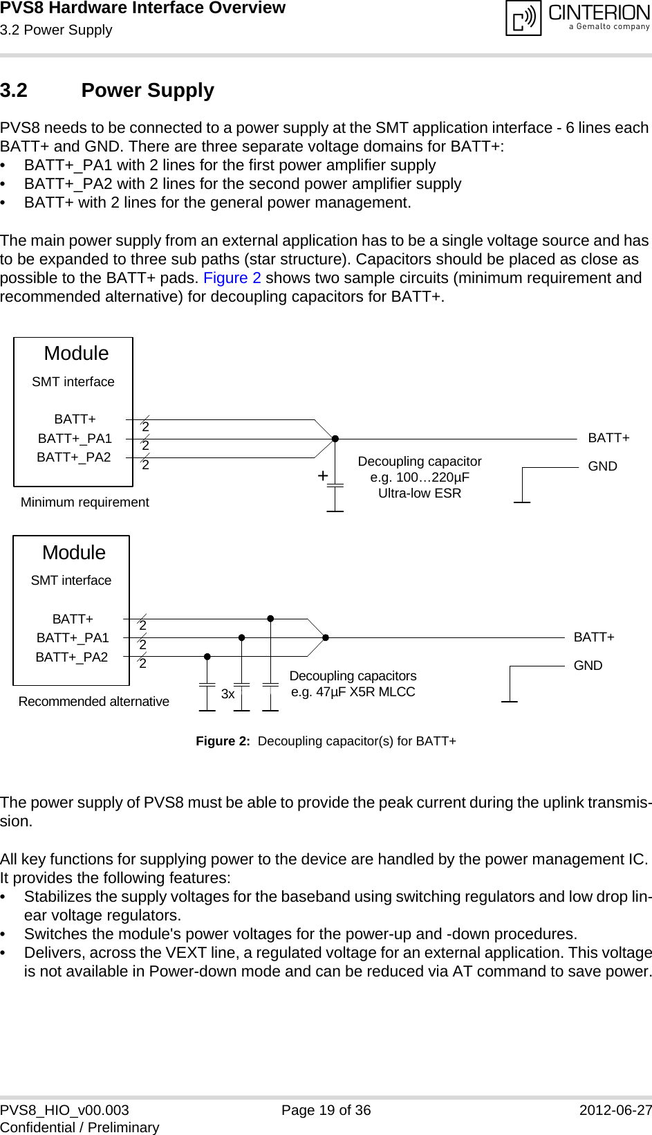
THALES DIS AlS Deutschland PVS8 Dual-Band CDMA-2000/EV-DO RF Module User Manual hid
Gemalto M2M GmbH Dual-Band CDMA-2000/EV-DO RF Module hid
UserManual.wiki
>
THALES DIS AlS Deutschland
>
PVS8 User Manual
>
user manual
Contents
1.
user manual
2.
integration manual
3.
Integration Manual
user manual
Navigation menu
Upload a User Manual
Namespaces
Wiki Guide
HTML
PDF
Info
Views
User Manual
Discussion / Help
Navigation
![PVS8 Hardware Interface Overview1 Introduction13PVS8_HIO_v00.003 Page 6 of 36 2012-06-27Confidential / Preliminary1 IntroductionThe document1 describes the hardware of the PVS8 module, designed to connect to a cellular device application and the air interface. It helps you quickly retrieve interface specifications, electrical and mechanical details and information on the requirements to be considered for in-tegrating further components.1.1 Related Documents[1] PVS8 AT Command Set[2] PVS8 Release Notes[3] DSB75 Support Box - Evaluation Kit for Cinterion Wireless Modules[4] Application Note 48: SMT Module Integration1.2 Terms and Abbreviations1. The document is effective only if listed in the appropriate Release Notes as part of the technicaldocumentation delivered with your Cinterion Wireless Modules product.Abbreviation DescriptionAGPS Assisted GPSANSI American National Standards InstituteAMR Adaptive MultirateARP Antenna Reference PointBB BasebandBC Band ClassBEP Bit Error ProbabilityBTS Base Transceiver StationCB or CBM Cell Broadcast MessageCDMA Code Division Multiple AccessCE Conformité Européene (European Conformity)CS Coding SchemeCS Circuit SwitchedCSD Circuit Switched DataCTM Cellular Text ModemDAC Digital-to-Analog ConverterDCS Digital Cellular SystemDL Download](https://usermanual.wiki/THALES-DIS-AlS-Deutschland/PVS8.user-manual/User-Guide-1735420-Page-6.png)
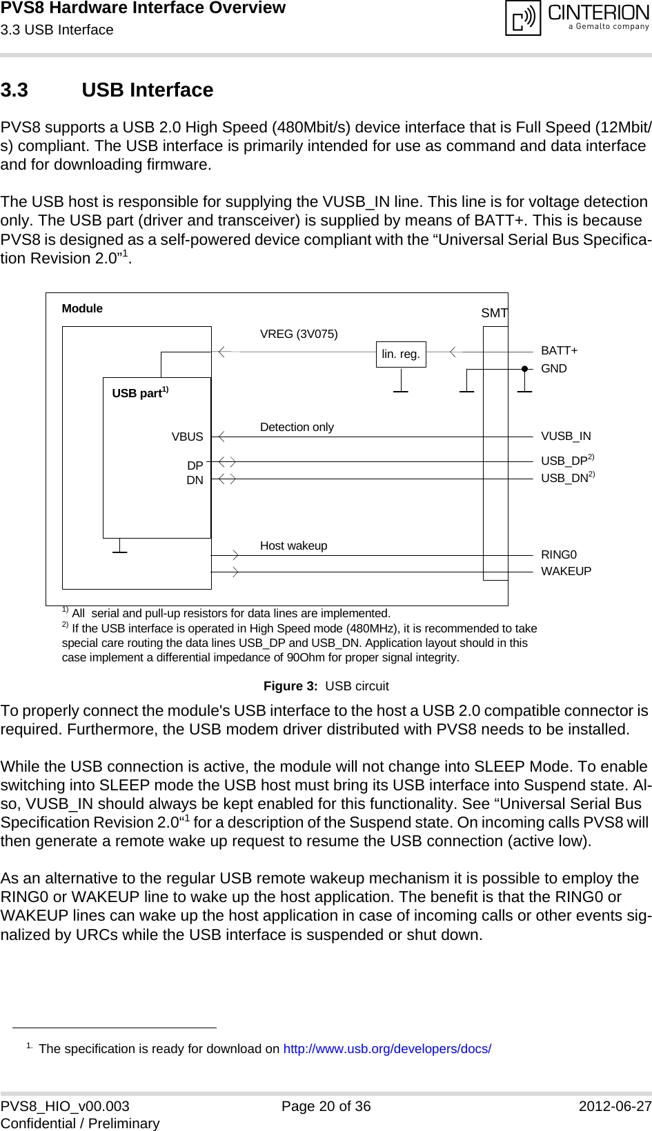
![PVS8 Hardware Interface Overview2.1 Key Features at a Glance16PVS8_HIO_v00.003 Page 15 of 36 2012-06-27Confidential / PreliminaryInterfacesModule interface Surface mount device with solderable connection pads (SMT application interface).Land grid array (LGA) technology ensures high solder joint reliability and provides the possibility to use an optional module mounting socket.For more information on how to integrate SMT modules see also [4]. This application note comprises chapters on module mounting and application layout issues as well as on additional SMT application development equipment.Antenna 50Ohms. CDMA main antenna, CDMA diversity antenna, GPS antenna (active/passive) USB USB 2.0 High Speed (480Mbit/s) device interface, Full Speed (12Mbit/s) compliantSerial interface ASC0:• 8-wire modem interface with status and control lines, unbalanced,asynchronous• Adjustable baud rates from 9,600bps up to 921,600bps• Supports RTS0/CTS0 hardware flow control• Multiplex ability according to GSM 07.10 Multiplexer ProtocolStatus Signal line to indicate network connectivity stateAudio 1 analog interface with microphone feeding1 digital interface: PCM or I2SPower on/off, ResetPower on/off Switch-on by hardware signal IGTSwitch-off by AT command (AT^SMSO)Automatic switch-off in case of critical temperature or voltage conditionsReset Orderly shutdown and reset by AT commandEmergency-off Emergency-off by hardware signal EMERG_OFF if IGT is not activeSpecial FeaturesPhonebook PhoneTTY/CTM support Integrated CTM modemAntenna SAIC (Single Antenna Interference Cancellation) / DARP (Downlink Advanced Receiver Performance)Rx diversity (receiver type 3i - 16-QAM)Over-the-air provisioning Verizon specific OTASP (Over-the-Air Service Provisioning) and OTAPA (Over-the-Air Parameter Administration)Evaluation kitEvaluation module PVS8 module soldered onto a dedicated PCB that can be connected to an adapter in order to be mounted onto the DSB75.DSB75 DSB75 Development Support Board designed to test and type approve Cinterion Wireless Modules and provide a sample configuration for appli-cation engineering. A special adapter is required to connect the PVS8 evaluation module to the DSB75.Feature Implementation](https://usermanual.wiki/THALES-DIS-AlS-Deutschland/PVS8.user-manual/User-Guide-1735420-Page-15.png)
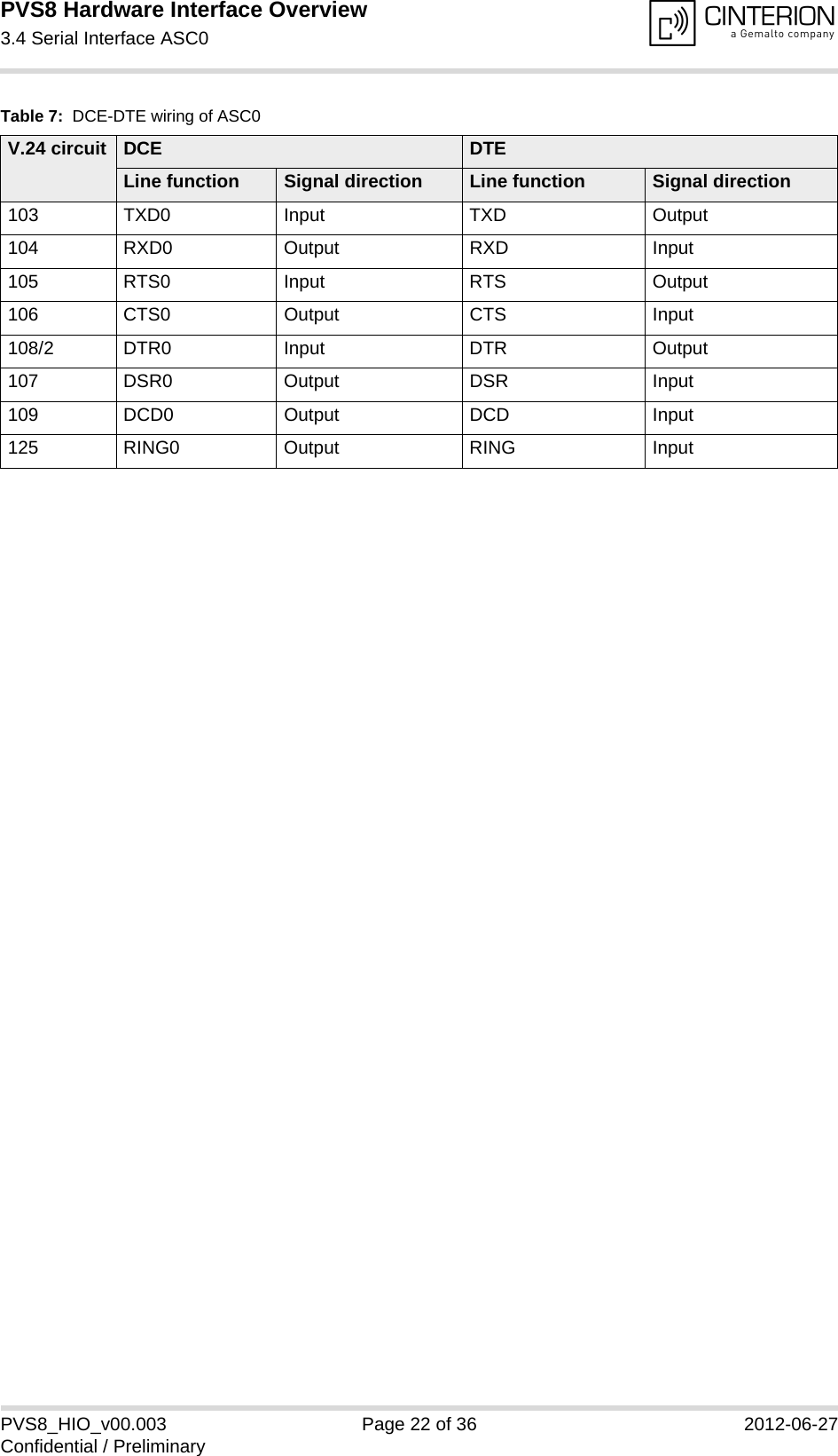
![PVS8 Hardware Interface Overview3.1 Operating Modes24PVS8_HIO_v00.003 Page 18 of 36 2012-06-27Confidential / Preliminary3.1 Operating ModesThe table below briefly summarizes the various operating modes referred to in the following chapters.Table 6: Overview of operating modesMode FunctionNormal operation CDMA SLEEP Power saving set automatically when no call is in progress and the USB connection is suspended by host or not present and no active commu-nication via ASC0. CDMA IDLE Power saving disabled (see [1]: AT^SCFG "MEopMode/PwrSave",<PwrSaveMode>) or an USB connection not suspended, but no call in progress.CDMA TALK/CDMA DATA CDMA data transfer in progress. Power consumption depends on net-work settings and data transfer rate.Power Down Normal shutdown after sending the AT^SMSO command. Only a voltage regulator is active for powering the RTC. Software is not active. Interfaces are not accessible. Operating volt-age (connected to BATT+) remains applied.Airplane mode Airplane mode shuts down the radio part of the module, causes the module to log off from the CDMA network and disables all AT commands whose execution requires a radio con-nection.Airplane mode can be controlled by AT command (see [1]).](https://usermanual.wiki/THALES-DIS-AlS-Deutschland/PVS8.user-manual/User-Guide-1735420-Page-18.png)
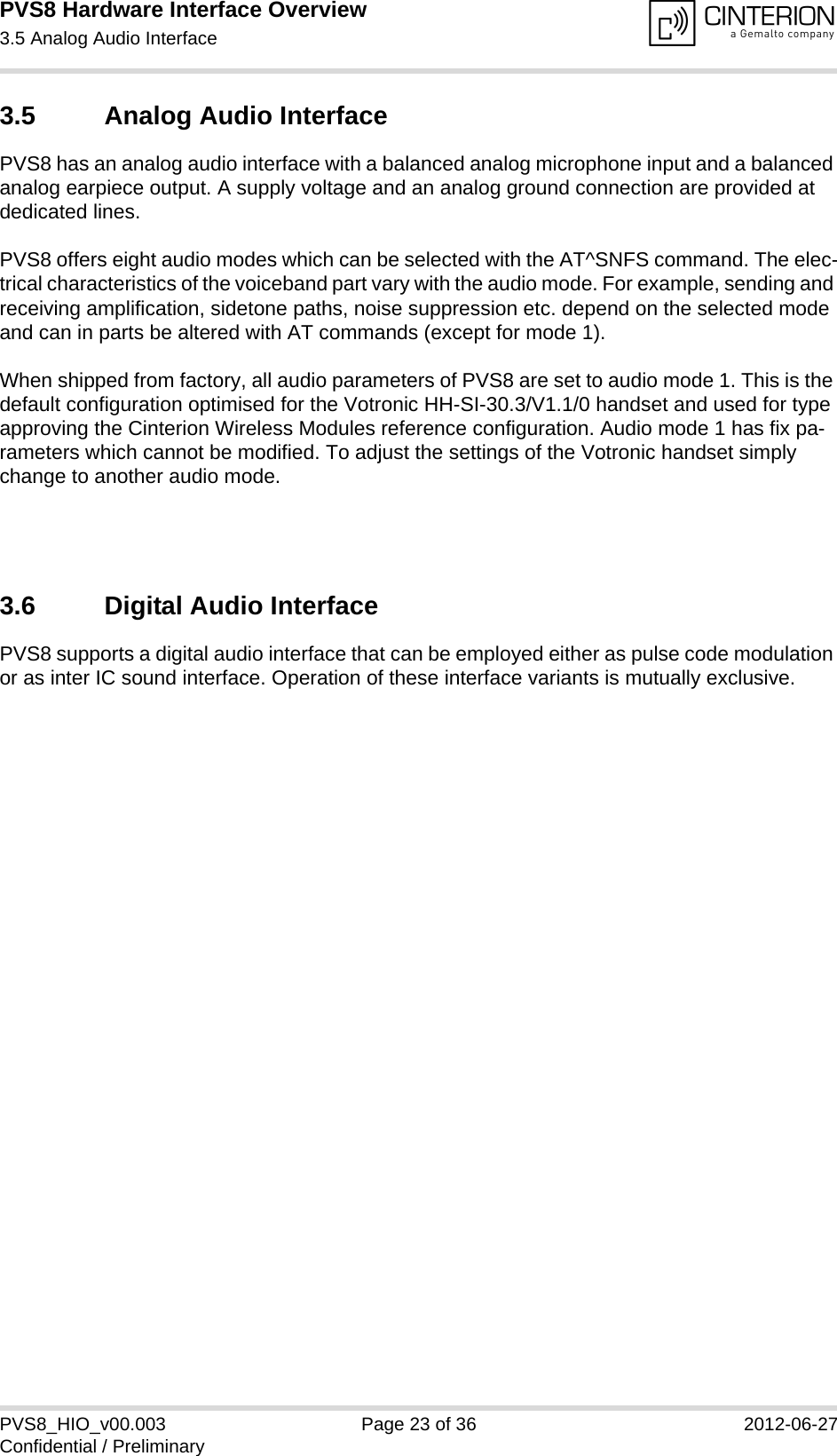
![PVS8 Hardware Interface Overview3.4 Serial Interface ASC024PVS8_HIO_v00.003 Page 21 of 36 2012-06-27Confidential / Preliminary3.4 Serial Interface ASC0PVS8 offers an 8-wire unbalanced, asynchronous modem interface ASC0 conforming to ITU-T V.24 protocol DCE signalling. The electrical characteristics do not comply with ITU-T V.28. The significant levels are 0V (for low data bit or active state) and 1.8V (for high data bit or in-active state). PVS8 is designed for use as a DCE. Based on the conventions for DCE-DTE connections it communicates with the customer application (DTE) using the following signals:• Port TXD @ application sends data to the module’s TXD0 signal line• Port RXD @ application receives data from the module’s RXD0 signal lineFigure 4: Serial interface ASC0Features:• Includes the data lines TXD0 and RXD0, the status lines RTS0 and CTS0 and, in addition,the modem control lines DTR0, DSR0, DCD0 and RING0.• ASC0 is designed for controlling voice calls, transferring data and for controlling the modulewith AT commands.• Full multiplexing capability allows the interface to be partitioned into virtual channels.• The RING0 signal serves to indicate incoming calls and other types of URCs (UnsolicitedResult Code). It can also be used to send pulses to the host application, for example towake up the application from power saving state. See [1] for details on how to configure theRING0 line by AT^SCFG.• Configured for 8 data bits, no parity and 1 stop bit. • ASC0 can be operated at fixed bit rates from 9600bps up to 921600bps.• Supports RTS0/CTS0 hardware flow control.• Wake up from SLEEP mode by RTS0 activation (high to low transition). Note. If the ASC0 serial interface is the application’s only interface, it is suggested to connect test points on the USB signal lines as a potential tracing possibility.](https://usermanual.wiki/THALES-DIS-AlS-Deutschland/PVS8.user-manual/User-Guide-1735420-Page-21.png)
![PVS8 Hardware Interface Overview4 GPS Receiver24PVS8_HIO_v00.003 Page 24 of 36 2012-06-27Confidential / Preliminary4 GPS ReceiverPVS8 integrates a GPS receiver that offers the full performance of GPS technology. The GPS receiver is able to continuously track all satellites in view, thus providing accurate satellite posi-tion data. The integrated GPS receiver supports the NMEA protocol via USB or ASC0 interface1. NMEA is a combined electrical and data specification for communication between various (marine) electronic devices including GPS receivers. It has been defined and controlled by the US-based National Marine Electronics Association. For more information on the NMEA Standard please refer to http://www.nmea.org.Depending on the receiver’s knowledge of last position, current time and ephemeris data, the receiver’s startup time (i.e., TTFF = Time-To-First-Fix) may vary: If the receiver has no knowl-edge of its last position or time, a startup takes considerably longer than if the receiver has still knowledge of its last position, time and almanac or has still access to valid ephimeris data and the precise time. By default, the GPS receiver is switched off. It has to be switched on and configured using AT commands. For more information on how to control the GPS interface via the AT command AT^SGPSC see [1].1. Using the serial ASC0 interface NMEA data is transmitted at a fixed speed of 115200bps.](https://usermanual.wiki/THALES-DIS-AlS-Deutschland/PVS8.user-manual/User-Guide-1735420-Page-24.png)
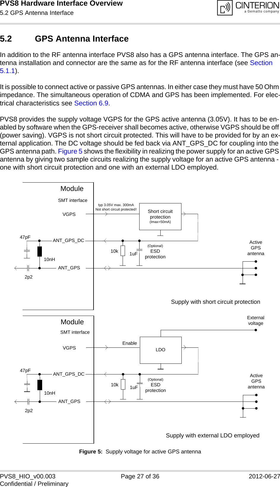
![PVS8 Hardware Interface Overview5 Antenna Interfaces28PVS8_HIO_v00.003 Page 25 of 36 2012-06-27Confidential / Preliminary5 Antenna Interfaces5.1 CDMA Antenna InterfaceThe PVS8 CDMA antenna interface comprises a main CDMA antenna as well as an optional CDMA Rx diversity antenna to improve signal reliability and quality1. The interface has an im-pedance of 50. PVS8 is capable of sustaining a total mismatch at the antenna interface with-out any damage, even when transmitting at maximum RF power.The external antenna must be matched properly to achieve best performance regarding radi-ated power, modulation accuracy and harmonic suppression. Matching networks are not in-cluded on the PVS8 PCB and should be placed in the host application, if the antenna does not have an impedance of 50.Regarding the return loss PVS8 provides the following values in the active band:1. By delivery default the optional CDMA Rx diversity antenna is configured as available for the module. Toavoid negative side effects and performance degradation it is recommended to disable the diversity an-tenna path if - the host application does not support a diversity antenna- the host application includes a diversity antenna - but a network simulator is used for development andperformance tests.Please refer to [1] for details on how to configure antenna settings. Table 8: Return loss in the active bandState of module Return loss of module Recommended return loss of applicationReceive > 8dB > 12dBTransmit not applicable > 12dBIdle < 5dB not applicable](https://usermanual.wiki/THALES-DIS-AlS-Deutschland/PVS8.user-manual/User-Guide-1735420-Page-25.png)
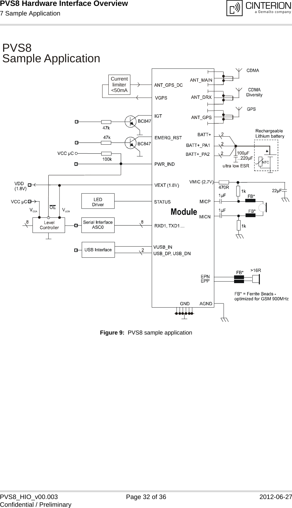
![PVS8 Hardware Interface Overview7 Sample Application32PVS8_HIO_v00.003 Page 31 of 36 2012-06-27Confidential / Preliminary7 Sample ApplicationFigure 9 shows a typical example of how to integrate an PVS8 module with an application. The audio interface demonstrates the balanced connection of microphone and earpiece. This solution is particularly well suited for internal transducers.The PWR_IND line is an open collector that needs an external pull-up resistor which connects to the voltage supply VCC µC of the microcontroller. Low state of the open collector pulls the PWR_IND signal low and indicates that the PVS8 module is active, high level notifies the Pow-er-down mode. If the module is in Power-down mode avoid current flowing from any other source into the mod-ule circuit, for example reverse current from high state external control lines. Therefore, the controlling application must be designed to prevent reverse flow. If an external level controller is required, this can be done by using for example a 5V I/O tolerant buffer/driver like a "74AVC4T245" with OE (Output Enable) controlled by PWR_IND.While developing SMT applications it is strongly recommended to provide test pointsfor certain signals resp. lines to and from the module - for debug and/or test purposes.The SMT application should allow for an easy access to these signals. For details onhow to implement test points see [4].The EMC measures are best practice recommendations. In fact, an adequate EMC strategy for an individual application is very much determined by the overall layout and, especially, the po-sition of components. Disclaimer:No warranty, either stated or implied, is provided on the sample schematic diagram shown in Figure 9 and the information detailed in this section. As functionality and compliance with na-tional regulations depend to a great amount on the used electronic components and the indi-vidual application layout manufacturers are required to ensure adequate design and operating safeguards for their products using PVS8 modules.](https://usermanual.wiki/THALES-DIS-AlS-Deutschland/PVS8.user-manual/User-Guide-1735420-Page-31.png)