THALES DIS AlS Deutschland TC65 Quadband GSM/GPRS Module User Manual TC65
Gemalto M2M GmbH Quadband GSM/GPRS Module TC65
Contents
- 1. Users Manual 1 of 2
- 2. Users Manual 2 of 2
Users Manual 1 of 2
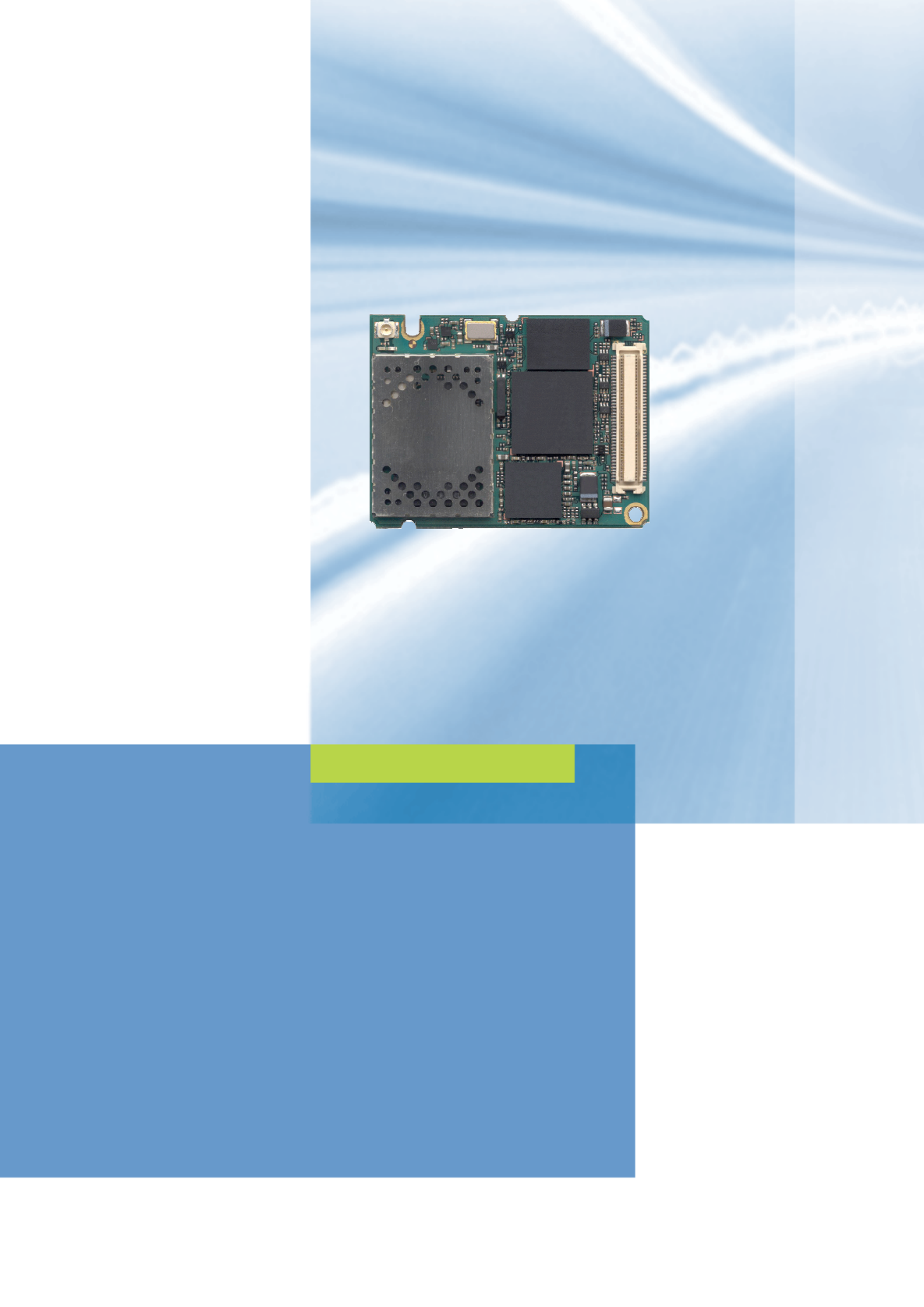

TC65 Hardware Interface Description
Strictly confidential / Draft s
TC65_HD_V00.450 Page 2 of 96 20.04.2005
Document Name: TC65 Hardware Interface Description
Version: 00.450
Date: April 20, 2005
DocId: TC65_HD_V00.450
Status: Strictly confidential / Draft
General note
Product is deemed accepted by Recipient and is provided without interface to Recipient´s products.
The Product constitutes pre-release version and code and may be changed substantially before
commercial release. The Product is provided on an “as is” basis only and may contain deficiencies or
inadequacies. The Product is provided without warranty of any kind, express or implied. To the
maximum extent permitted by applicable law, Siemens further disclaims all warranties, including
without limitation any implied warranties of merchantability, fitness for a particular purpose and
noninfringement of third-party rights. The entire risk arising out of the use or performance of the
Product and documentation remains with Recipient. This Product is not intended for use in life support
appliances, devices or systems where a malfunction of the product can reasonably be expected to
result in personal injury. Applications incorporating the described product must be designed to be in
accordance with the technical specifications provided in these guidelines. Failure to comply with any
of the required procedures can result in malfunctions or serious discrepancies in results. Furthermore,
all safety instructions regarding the use of mobile technical systems, including GSM products, which
also apply to cellular phones must be followed. Siemens AG customers using or selling this product
for use in any applications do so at their own risk and agree to fully indemnify Siemens for any
damages resulting from illegal use or resale. To the maximum extent permitted by applicable law, in
no event shall Siemens or its suppliers be liable for any consequential, incidental, direct, indirect,
punitive or other damages whatsoever (including, without limitation, damages for loss of business
profits, business interruption, loss of business information or data, or other pecuniary loss) arising out
the use of or inability to use the Product, even if Siemens has been advised of the possibility of such
damages. Subject to change without notice at any time.
Copyright
Transmittal, reproduction, dissemination and/or editing of this document as well as utilization of its
contents and communication thereof to others without express authorization are prohibited. Offenders
will be held liable for payment of damages. All rights created by patent grant or registration of a utility
model or design patent are reserved.
Copyright © Siemens AG 2005

TC65 Hardware Interface Description
Strictly confidential / Draft s
TC65_HD_V00.450 Page 3 of 96 20.04.2005
Contents
0 Document History .........................................................................................................7
1 Introduction ...................................................................................................................8
1.1 Related Documents ...............................................................................................8
1.2 Terms and Abbreviations.......................................................................................9
1.3 Type Approval......................................................................................................12
1.4 Safety Precautions...............................................................................................14
2 Product Concept .........................................................................................................16
2.1 Key Features at a Glance ....................................................................................16
2.2 TC65 System Overview .......................................................................................19
2.3 Circuit Concept ....................................................................................................20
3 Application Interface...................................................................................................21
3.1 Operating Modes .................................................................................................22
3.2 Power Supply.......................................................................................................24
3.2.1 Minimizing Power Losses ......................................................................24
3.2.2 Measuring the Supply Voltage VBATT+ ....................................................25
3.2.3 Monitoring Power Supply by AT Command ...........................................25
3.3 Power Up / Power Down Scenarios.....................................................................26
3.3.1 Turn on TC65.........................................................................................26
3.3.1.1 Turn on TC65 Using Ignition Line IGT ...................................................26
3.3.1.2 Turn on TC65 Using the VCHARGE Signal...........................................28
3.3.1.3 Reset TC65 via AT+CFUN Command ...................................................29
3.3.1.4 Reset TC65 in Case of Emergency via EMERG_RST ..........................29
3.3.2 Turn off TC65.........................................................................................30
3.3.2.1 Turn off TC65 Using AT Command .......................................................30
3.3.2.2 Leakage Current in Power Down Mode .................................................31
3.3.3 Automatic Shutdown ..............................................................................32
3.3.3.1 Temperature Dependent Shutdown.......................................................32
3.3.3.2 Temperature Control during Emergency call .........................................33
3.3.3.3 Undervoltage Shutdown if Battery NTC is Present ................................33
3.3.3.4 Undervoltage Shutdown if no Battery NTC is Present ...........................34
3.3.3.5 Overvoltage Shutdown...........................................................................34
3.4 Automatic GPRS Multislot Class Change............................................................35
3.5 Charging Control..................................................................................................36
3.5.1 Hardware Requirements ........................................................................36
3.5.2 Software Requirements .........................................................................36
3.5.3 Battery Pack Requirements ...................................................................37
3.5.4 Batteries Recommended for Use with TC65..........................................38
3.5.5 Charger Requirements...........................................................................39
3.5.6 Implemented Charging Technique.........................................................39
3.5.7 Operating Modes during Charging.........................................................40
3.6 Summary of State Transitions (Except SLEEP Mode).........................................42
3.7 RTC Backup ........................................................................................................43
3.8 SIM Interface .......................................................................................................44
3.9 Serial Interface ASC0 ..........................................................................................45
3.10 Serial Interface ASC1 ..........................................................................................47
3.11 USB Interface ......................................................................................................48
3.11.1 Installing the USB Modem Driver...........................................................49
3.12 I2C Interface .........................................................................................................51
3.13 Audio Interfaces...................................................................................................53

TC65 Hardware Interface Description
Strictly confidential / Draft s
TC65_HD_V00.450 Page 4 of 96 20.04.2005
3.13.1 Speech Processing................................................................................54
3.13.2 Microphone Circuit.................................................................................54
3.13.2.1 Single-ended Microphone Input.............................................................54
3.13.2.2 Differential Microphone Input.................................................................55
3.13.2.3 Line Input Configuration with OpAmp ....................................................56
3.13.3 Loudspeaker Circuit...............................................................................57
3.13.4 Digital Audio Interface DAI.....................................................................58
3.14 Control Signals ....................................................................................................59
3.14.1 Synchronization Signal ..........................................................................59
3.14.2 Using the SYNC Pin to Control a Status LED........................................60
4 Antenna Interface........................................................................................................61
4.1 Antenna Installation .............................................................................................61
4.2 Antenna Pad ........................................................................................................63
4.2.1 Suitable Cable Types.............................................................................63
4.3 Antenna Connector..............................................................................................64
5 Electrical, Reliability and Radio Characteristics......................................................68
5.1 Absolute Maximum Ratings .................................................................................68
5.2 Operating Temperatures......................................................................................68
5.3 Pin Assignment and Signal Description...............................................................69
5.4 Power Supply Ratings .........................................................................................75
5.5 Electrostatic Discharge ........................................................................................77
5.6 Reliability Characteristics.....................................................................................78
6 Mechanics....................................................................................................................79
6.1 Mechanical Dimensions of TC65 .........................................................................79
6.2 Mounting TC65 to the Application Platform .........................................................81
6.3 Board-to-Board Application Connector ................................................................82
7 Sample Application.....................................................................................................85
8 Reference Approval ....................................................................................................87
8.1 Reference Equipment for Type Approval.............................................................87
8.2 Compliance with FCC Rules and Regulations.....................................................88
9 Appendix......................................................................................................................89
9.1 List of Parts and Accessories ..............................................................................89
9.2 Fasteners and Fixings for Electronic Equipment .................................................91
9.2.1 Fasteners from German Supplier ETTINGER GmbH ............................91
9.3 Data Sheets of Recommended Batteries ............................................................94

TC65 Hardware Interface Description
Strictly confidential / Draft s
TC65_HD_V00.450 Page 5 of 96 20.04.2005
Tables
Table 1: Overview of operating modes................................................................................... 22
Table 2: Temperature dependent behavior ............................................................................ 33
Table 3: Specifications of battery packs suitable for use with TC65 ...................................... 38
Table 4: Comparison Charge-only and Charge mode............................................................ 41
Table 5: AT commands available in Charge-only mode......................................................... 41
Table 6: State transitions of TC65 (except SLEEP mode) .....................................................42
Table 7: Signals of the SIM interface (board-to-board connector) ......................................... 44
Table 8: DCE-DTE wiring of ASC0......................................................................................... 46
Table 9: DCE-DTE wiring of ASC1......................................................................................... 47
Table 11: Return loss in the active band ................................................................................61
Table 12: Product specifications of U.FL-R-SMT connector .................................................. 64
Table 13: Material and finish of U.FL-R-SMT connector and recommended plugs ...............65
Table 14: Ordering information for Hirose U.FL Series .......................................................... 67
Table 15: Absolute maximum ratings under non-operating conditions .................................. 68
Table 16: Operating temperatures ......................................................................................... 68
Table 17: Signal description...................................................................................................70
Table 18: Power supply ratings .............................................................................................. 75
Table 19: Current consumption during transmit burst ............................................................ 76
Table 20: Measured electrostatic values................................................................................77
Table 21: Summary of reliability test conditions ..................................................................... 78
Table 22: Technical specifications of Molex board-to-board connector .................................82
Table 23: List of parts and accessories..................................................................................89
Table 24: Molex sales contacts (subject to change) ..............................................................90
Table 25: Hirose sales contacts (subject to change)..............................................................90
Figures
Figure 1: TC65 system overview............................................................................................ 19
Figure 2: TC65 block diagram ................................................................................................20
Figure 3: Power supply limits during transmit burst................................................................ 25
Figure 4: Position of the reference points BATT+ and GND .................................................. 25
Figure 5: Power-on with operating voltage at BATT+ applied before activating IGT.............. 27
Figure 6: Power-on with IGT held low before switching on operating voltage at BATT+ .......28
Figure 7: Signal states during turn-off procedure ...................................................................31
Figure 8: Battery pack circuit diagram....................................................................................37
Figure 9: RTC supply from capacitor...................................................................................... 43
Figure 10: RTC supply from rechargeable battery .................................................................43
Figure 11: RTC supply from non-chargeable battery .............................................................43
Figure 12: Serial interface ASC0............................................................................................ 45
Figure 13: Serial interface ASC1............................................................................................ 47
Figure 14: USB circuit ............................................................................................................48
Figure 15: I2C interface connected to VCC of application .....................................................51
Figure 16: I2C interface connected to VEXT line of TC65 ..................................................... 52
Figure 17: Audio block diagram.............................................................................................. 53
Figure 18: Single ended microphone input............................................................................. 54
Figure 19: Differential microphone input ................................................................................55
Figure 20: Line input configuration with OpAmp .................................................................... 56
Figure 21: Differential loudspeaker configuration...................................................................57
Figure 22: Single ended loudspeaker configuration............................................................... 57
Figure 25: SYNC signal during transmit burst ........................................................................ 59
Figure 26: LED Circuit (Example)...........................................................................................60

TC65 Hardware Interface Description
Strictly confidential / Draft s
TC65_HD_V00.450 Page 6 of 96 20.04.2005
Figure 27: Never use antenna connector and antenna pad at the same time ....................... 62
Figure 28: Restricted area around antenna pad..................................................................... 62
Figure 29: Mechanical dimensions of U.FL-R-SMT connector...............................................64
Figure 30: U.FL-R-SMT connector with U.FL-LP-040 plug ....................................................65
Figure 31: U.FL-R-SMT connector with U.FL-LP-066 plug ....................................................65
Figure 32: Specifications of U.FL-LP-(V)-040(01) plug .......................................................... 66
Figure 33: Pin assignment (component side of TC65) ........................................................... 69
Figure 34: TC65 – top view .................................................................................................... 79
Figure 35: Dimensions of TC65.............................................................................................. 80
Figure 36: Molex board-to-board connector 52991-0808 on TC65 ........................................ 83
Figure 37: Mating board-to-board connector 53748-0808 on application ..............................84
Figure 38: TC65 sample application (draft) ............................................................................86
Figure 39: Reference equipment for Type Approval .............................................................. 87
Figure 40: Lithium Ion battery from VARTA ...........................................................................95
Figure 41: Lithium Polymer battery from VARTA ................................................................... 96
TC65 Hardware Interface Description
Strictly confidential / Draft s
TC65_HD_V00.450 Page 7 of 96 20.04.2005
0 Document History
Preceding document: "TC65 Hardware Interface Description" Version 00.302
New document: "TC65 Hardware Interface Description" Version 00.450
Chapter What is new
Throughout
manual
IGT line needs to be driven low for at least 400ms
2.1 Updated description of I2C and SPI.
3.1 New chapter: Operating Modes
3.3.1 Added remarks on different operating modes.
3.3.3.3 Added remark on shutdown threshold in IDLE mode.
3.5.2 New chapter to describe requirements to control end of charging.
3.5.4 Updated recommended battery specifications.
3.5.7 Added remark on how to switch the module off when in Charging-only mode.
3.6 New chapter: Summary of State Transitions (Except SLEEP Mode)
3.12 More detailed description of AT^SSPI.
3.14.1 Updated forward time of SYNC signal during transmit burst.
5.2 Added remark on temperature tolerances.
5.3 Renamed pins of I2C and SPI.
5.4 Changed table “Current consumption during transmit burst”

TC65 Hardware Interface Description
Strictly confidential / Draft s
TC65_HD_V00.450 Page 8 of 96 20.04.2005
1 Introduction
This document describes the hardware of the Siemens TC65 module that connects to the
cellular device application and the air interface. It helps you quickly retrieve interface
specifications, electrical and mechanical details and information on the requirements to be
considered for integrating further components.
1.1 Related Documents
[1] TC65 AT Command Set
[2] TC65 Release Notes 00.450
[3] DSB75 Support Box - Evaluation Kit for Siemens Cellular Engines
[4] Application 07: Rechargeable Lithium Batteries in GSM Applications (not yet available)
[5] Multiplexer User's Guide (not yet available)

TC65 Hardware Interface Description
Strictly confidential / Draft s
TC65_HD_V00.450 Page 9 of 96 20.04.2005
1.2 Terms and Abbreviations
Abbreviation Description
ADC Analog-to-Digital Converter
AGC Automatic Gain Control
ANSI American National Standards Institute
ARFCN Absolute Radio Frequency Channel Number
ARP Antenna Reference Point
ASC0 / ASC1 Asynchronous Controller. Abbreviations used for first and second serial interface of
TC65
B Thermistor Constant
B2B Board-to-board connector
BER Bit Error Rate
BTS Base Transceiver Station
CB or CBM Cell Broadcast Message
CE Conformité Européene (European Conformity)
CHAP Challenge Handshake Authentication Protocol
CPU Central Processing Unit
CS Coding Scheme
CSD Circuit Switched Data
CTS Clear to Send
DAC Digital-to-Analog Converter
DAI Digital Audio Interface
dBm0 Digital level, 3.14dBm0 corresponds to full scale, see ITU G.711, A-law
DCE Data Communication Equipment (typically modems, e.g. Siemens GSM engine)
DCS 1800 Digital Cellular System, also referred to as PCN
DRX Discontinuous Reception
DSB Development Support Box
DSP Digital Signal Processor
DSR Data Set Ready
DTE Data Terminal Equipment (typically computer, terminal, printer or, for example, GSM
application)
DTR Data Terminal Ready
DTX Discontinuous Transmission
EFR Enhanced Full Rate
EGSM Enhanced GSM
EIRP Equivalent Isotropic Radiated Power
EMC Electromagnetic Compatibility
ERP Effective Radiated Power

TC65 Hardware Interface Description
Strictly confidential / Draft s
TC65_HD_V00.450 Page 10 of 96 20.04.2005
Abbreviation Description
ESD Electrostatic Discharge
ETS European Telecommunication Standard
FCC Federal Communications Commission (U.S.)
FDMA Frequency Division Multiple Access
FR Full Rate
GMSK Gaussian Minimum Shift Keying
GPIO General Purpose Input/Output
GPRS General Packet Radio Service
GSM Global Standard for Mobile Communications
HiZ High Impedance
HR Half Rate
I/O Input/Output
IC Integrated Circuit
IMEI International Mobile Equipment Identity
ISO International Standards Organization
ITU International Telecommunications Union
kbps kbits per second
LED Light Emitting Diode
Li-Ion / Li+ Lithium-Ion
Li battery Rechargeable Lithium Ion or Lithium Polymer battery
Mbps Mbits per second
MMI Man Machine Interface
MO Mobile Originated
MS Mobile Station (GSM engine), also referred to as TE
MSISDN Mobile Station International ISDN number
MT Mobile Terminated
NTC Negative Temperature Coefficient
OEM Original Equipment Manufacturer
PA Power Amplifier
PAP Password Authentication Protocol
PBCCH Packet Switched Broadcast Control Channel
PCB Printed Circuit Board
PCL Power Control Level
PCM Pulse Code Modulation
PCN Personal Communications Network, also referred to as DCS 1800
PCS Personal Communication System, also referred to as GSM 1900
PDU Protocol Data Unit
PLL Phase Locked Loop

TC65 Hardware Interface Description
Strictly confidential / Draft s
TC65_HD_V00.450 Page 11 of 96 20.04.2005
Abbreviation Description
PPP Point-to-point protocol
PSK Phase Shift Keying
PSU Power Supply Unit
R&TTE Radio and Telecommunication Terminal Equipment
RAM Random Access Memory
RF Radio Frequency
RMS Root Mean Square (value)
ROM Read-only Memory
RTC Real Time Clock
RTS Request to Send
Rx Receive Direction
SAR Specific Absorption Rate
SELV Safety Extra Low Voltage
SIM Subscriber Identification Module
SMS Short Message Service
SPI Serial Peripheral Interface
SRAM Static Random Access Memory
TA Terminal adapter (e.g. GSM engine)
TDMA Time Division Multiple Access
TE Terminal Equipment, also referred to as DTE
Tx Transmit Direction
UART Universal asynchronous receiver-transmitter
URC Unsolicited Result Code
USB Universal Serial Bus
USSD Unstructured Supplementary Service Data
VSWR Voltage Standing Wave Ratio
Phonebook abbreviations
FD SIM fixdialing phonebook
LD SIM last dialing phonebook (list of numbers most recently dialed)
MC Mobile Equipment list of unanswered MT calls (missed calls)
ME Mobile Equipment phonebook
ON Own numbers (MSISDNs) stored on SIM or ME
RC Mobile Equipment list of received calls
SM SIM phonebook

TC65 Hardware Interface Description
Strictly confidential / Draft s
TC65_HD_V00.450 Page 12 of 96 20.04.2005
1.3 Type Approval
TC65 is designed to comply with the directives and standards listed below. Please note that
the product is still in a pre-release state and, therefore, type approval and testing procedures
have not yet been completed.
European directives
99/05/EC “Directive of the European Parliament and of the council of 9 March
1999 on radio equipment and telecommunications terminal
equipment and the mutual recognition of their conformity”, in short
referred to as R&TTE Directive 1999/5/EC
89/336/EC Directive on electromagnetic compatibility
73/23/EC Directive on electrical equipment designed for use within certain
voltage limits (Low Voltage Directive)
Standards of North American Type Approval
CFR Title 47 “Code of Federal Regulations, Part 22 and Part 24 (Telecommuni-
cations, PCS)”; US Equipment Authorization FCC
UL 60 950 “Product Safety Certification” (Safety requirements)
NAPRD.03 “Overview of PCS Type certification review board
Mobile Equipment Type Certification and IMEI control”
PCS Type Certification Review board (PTCRB), Version 3.1.0
RSS133 (Issue2) Canadian Standard
Standards of European Type Approval
3GPP TS 51.010-1 “Digital cellular telecommunications system (Phase 2); Mobile
Station (MS) conformance specification”
ETSI EN 301 511 “V7.0.1 (2000-12) Candidate Harmonized European Standard
(Telecommunications series) Global System for Mobile
communications (GSM); Harmonized standard for mobile stations in
the GSM 900 and DCS 1800 bands covering essential requirements
under article 3.2 of the R&TTE directive (1999/5/EC) (GSM 13.11
version 7.0.1 Release 1998)”
GCF-CC “Global Certification Forum - Certification Criteria” V3.16.0
ETSI EN 301 489-1 “V1.2.1 Candidate Harmonized European Standard
(Telecommunications series) Electro Magnetic Compatibility and
Radio spectrum Matters (ERM); Electro Magnetic Compatibility
(EMC) standard for radio equipment and services; Part 1: Common
Technical Requirements”
ETSI EN 301 489-7 “V1.1.1 Candidate Harmonized European Standard
(Telecommunications series) Electro Magnetic Compatibility and
Radio spectrum Matters (ERM); Electro Magnetic Compatibility
(EMC) standard for radio equipment and services; Part 7: Specific
conditions for mobile and portable radio and ancillary equipment of
digital cellular radio telecommunications systems (GSM and DCS)”
EN 60 950 Safety of information technology equipment (2000)

TC65 Hardware Interface Description
Strictly confidential / Draft s
TC65_HD_V00.450 Page 13 of 96 20.04.2005
Requirements of quality
IEC 60068 Environmental testing
DIN EN 60529 IP codes
Compliance with international rules and regulations
Manufacturers of mobile or fixed devices incorporating TC65 modules are advised to have
their completed product tested and approved for compliance with all applicable national and
international regulations. As a quad-band GSM/GPRS engine designed for use on any GSM
network in the world, TC65 is required to pass all approvals relevant to operation on the
European and North American markets. For the North American market this includes the
Rules and Regulations of the Federal Communications Commission (FCC) and PTCRB, for
the European market the R&TTE Directives and GCF Certification Criteria must be fully
satisfied.
The FCC Equipment Authorization granted to the TC65 Siemens reference application is
valid only for the equipment described in Section 8.1.
SAR requirements specific to portable mobiles
Mobile phones, PDAs or other portable transmitters and receivers incorporating a GSM
module must be in accordance with the guidelines for human exposure to radio frequency
energy. This requires the Specific Absorption Rate (SAR) of portable TC65 based
applications to be evaluated and approved for compliance with national and/or international
regulations.
Since the SAR value varies significantly with the individual product design manufacturers are
advised to submit their product for approval if designed for portable use. For European and
US markets the relevant directives are mentioned below. It is the responsibility of the
manufacturer of the final product to verify whether or not further standards, recommendations
or directives are in force outside these areas.
Products intended for sale on US markets
ES 59005/ANSI C95.1 Considerations for evaluation of human exposure to
Electromagnetic Fields (EMFs) from Mobile Telecommunication
Equipment (MTE) in the frequency range 30MHz - 6GHz
Products intended for sale on European markets
EN 50360 Product standard to demonstrate the compliance of mobile phones
with the basic restrictions related to human exposure to
electromagnetic fields (300MHz - 3GHz)
Note: Usage of TC65 in a fixed, mobile or portable application is not allowed without a
new FCC certification.
TC65 Hardware Interface Description
Strictly confidential / Draft s
TC65_HD_V00.450 Page 14 of 96 20.04.2005
1.4 Safety Precautions
The following safety precautions must be observed during all phases of the operation, usage,
service or repair of any cellular terminal or mobile incorporating TC65. Manufacturers of the
cellular terminal are advised to convey the following safety information to users and
operating personnel and to incorporate these guidelines into all manuals supplied with the
product. Failure to comply with these precautions violates safety standards of design,
manufacture and intended use of the product. Siemens AG assumes no liability for
customer’s failure to comply with these precautions.
When in a hospital or other health care facility, observe the restrictions on the
use of mobiles. Switch the cellular terminal or mobile off, if instructed to do so
by the guidelines posted in sensitive areas. Medical equipment may be
sensitive to RF energy.
The operation of cardiac pacemakers, other implanted medical equipment
and hearing aids can be affected by interference from cellular terminals or
mobiles placed close to the device. If in doubt about potential danger, contact
the physician or the manufacturer of the device to verify that the equipment is
properly shielded. Pacemaker patients are advised to keep their hand-held
mobile away from the pacemaker, while it is on.
Switch off the cellular terminal or mobile before boarding an aircraft. Make
sure it cannot be switched on inadvertently. The operation of wireless
appliances in an aircraft is forbidden to prevent interference with
communications systems. Failure to observe these instructions may lead to
the suspension or denial of cellular services to the offender, legal action, or
both.
Do not operate the cellular terminal or mobile in the presence of flammable
gases or fumes. Switch off the cellular terminal when you are near petrol
stations, fuel depots, chemical plants or where blasting operations are in
progress. Operation of any electrical equipment in potentially explosive
atmospheres can constitute a safety hazard.
Your cellular terminal or mobile receives and transmits radio frequency
energy while switched on. Remember that interference can occur if it is used
close to TV sets, radios, computers or inadequately shielded equipment.
Follow any special regulations and always switch off the cellular terminal or
mobile wherever forbidden, or when you suspect that it may cause
interference or danger.
Road safety comes first! Do not use a hand-held cellular terminal or mobile
when driving a vehicle, unless it is securely mounted in a holder for
speakerphone operation. Before making a call with a hand-held terminal or
mobile, park the vehicle.
Speakerphones must be installed by qualified personnel. Faulty installation or
operation can constitute a safety hazard.

TC65 Hardware Interface Description
Strictly confidential / Draft s
TC65_HD_V00.450 Page 15 of 96 20.04.2005
SOS
IMPORTANT!
Cellular terminals or mobiles operate using radio signals and cellular
networks. Because of this, connection cannot be guaranteed at all times
under all conditions. Therefore, you should never rely solely upon any
wireless device for essential communications, for example emergency calls.
Remember, in order to make or receive calls, the cellular terminal or mobile
must be switched on and in a service area with adequate cellular signal
strength.
Some networks do not allow for emergency calls if certain network services or
phone features are in use (e.g. lock functions, fixed dialing etc.). You may
need to deactivate those features before you can make an emergency call.
Some networks require that a valid SIM card be properly inserted in the
cellular terminal or mobile.
TC65 Hardware Interface Description
Strictly confidential / Draft s
TC65_HD_V00.450 Page 16 of 96 20.04.2005
2 Product Concept
2.1 Key Features at a Glance
Feature Implementation
General
Frequency bands Quad band: GSM 850/900/1800/1900MHz
GSM class Small MS
Output power
(according to
Release 99, V5)
Class 4 (+33dBm ±2dB) for EGSM850
Class 4 (+33dBm ±2dB) for EGSM900
Class 1 (+30dBm ±2dB) for GSM1800
Class 1 (+30dBm ±2dB) for GSM1900
The values stated above are maximum limits. According to
Release 99, Version 5, the maximum output power in a multislot
configuration may be lower. The nominal reduction of maximum
output power varies with the number of uplink timeslots used and
amounts to 3.0dB for 2Tx, 4.8dB for 3Tx and 6.0dB for 4Tx.
Power supply 3.2V to 4.5V
Power consumption Sleep mode: max. TBD
Power down mode: typically 50µA
Java platform Java Virtual Machine with interfaces to AT Parser, Serial
Interface, FlashFileSystem and TCP/IP Stack.
Major benefits: seamless integration into Java applications, ease
of programming, no need for application microcontroller,
extremely cost-efficient hardware and software design – ideal
platform for industrial GSM applications.
Operating temperature -30°C to +65°C ambient temperature
Auto switch-off at +90°C board temperature (preliminary)
Physical Dimensions: 33.9mm x 44.6mm x max. 3.5mm
Weight: approx. 7.5g
GSM / GPRS features
Data transfer GPRS
• Multislot Class 12
• Full PBCCH support
• Mobile Station Class B
• Coding Scheme 1 – 4
CSD
• V.110, RLP, non-transparent
• 2.4, 4.8, 9.6, 14.4kbps
• USSD
PPP-stack for GPRS data transfer
TC65 Hardware Interface Description
Strictly confidential / Draft s
TC65_HD_V00.450 Page 17 of 96 20.04.2005
Feature Implementation
SMS • Point-to-point MT and MO
• Cell broadcast
• Text and PDU mode
• Storage: SIM card plus 25 SMS locations in mobile equipment
• Transmission of SMS alternatively over CSD or GPRS.
Preferred mode can be user defined.
Fax Group 3; Class 1
Audio Speech codecs:
• Half rate HR (ETS 06.20)
• Full rate FR (ETS 06.10)
• Enhanced full rate EFR (ETS 06.50/06.60/06.80)
• Adaptive Multi Rate AMR
Speakerphone operation, echo cancellation, noise suppression
DTMF, 7 ringing tones
Software
AT commands AT-Hayes GSM 07.05 and 07.07, Siemens
AT commands for RIL compatibility (NDIS/RIL)
MicrosoftTM compatibility RIL / NDIS for Pocket PC and Smartphone
SIM Application Toolkit SAT Release 99
TCP/IP stack Access by AT commands
IP addresses IP version 6
Remote SIM Access TC65 supports Remote SIM Access. RSA enables TC65 to use a
remote SIM card via its serial interface, in addition to the SIM card
locally attached to the dedicated lines of the application interface.
In a vehicle mounted scenario, for example, this allows the driver
to access a mobile phone brought into the car from a car-
embedded phone. The connection between both phones can be a
Bluetooth wireless link or a serial link, e.g. via the car cradle.
The necessary protocols and procedures are implemented
according to the “SIM Access Profile Interoperability Specification
of the Bluetooth Special Interest Group”.
Firmware update Download over serial interface ASC0
Download over SIM interface
Download over USB
Interfaces
2 serial interfaces
ASC0
• 8-wire modem interface with status and control lines,
unbalanced, asynchronous
• 1.2kbps to 460kbps
• Autobauding TBD
• Supports RTS0/CTS0 hardware handshake and software
XON/XOFF flow control.
• Multiplex ability according to GSM 07.10 Multiplexer Protocol.
TC65 Hardware Interface Description
Strictly confidential / Draft s
TC65_HD_V00.450 Page 18 of 96 20.04.2005
Feature Implementation
ASC1
• 4-wire, unbalanced asynchronous interface
• 1.2kbps to 460kbps
• Autobauding TBD
• Supports RTS1/CTS1 hardware handshake and software
XON/XOFF flow control
USB Supports a USB 2.0 Full Speed (12Mbit/s) slave interface.
I2C I2C bus for 7-bit addressing and transmission rates up to 400kbps.
Programmable with AT^SSPI command.
Alternatively, all pins of the I²C interface are configurable as SPI.
SPI Serial Peripheral Interface for transmission rates up to 6.5 Mbps.
Programmable with AT^SSPI command.
If the SPI is active the I²C interface is not available.
Audio • 2 analog interfaces
• 1 digital interface (PCM)
SIM interface Supported SIM cards: 3V, 1.8V
Antenna 50Ohms. External antenna can be connected via antenna
connector or solderable pad.
Module interface 80-pin board-to-board connector
Power on/off, Reset
Power on/off • Switch-on by hardware pin IGT
• Switch-off by AT command (AT^SMSO)
• Automatic switch-off in case of critical temperature and
voltage conditions.
Reset • Orderly shutdown and reset by AT command
• Emergency reset by hardware pin EMERG_RST
Special features
Charging Supports management of rechargeable Lithium Ion and Lithium
Polymer batteries
Real time clock Timer functions via AT commands
GPIO 10 I/O pins of the application interface programmable as GPIO.
Programming is done via AT commands.
Phonebook SIM and phone
Evaluation kit
DSB75 DSB75 Evaluation Board designed to test and type approve
Siemens cellular engines and provide a sample configuration for
application engineering.
TC65 Hardware Interface Description
Strictly confidential / Draft s
TC65_HD_V00.450 Page 19 of 96 20.04.2005
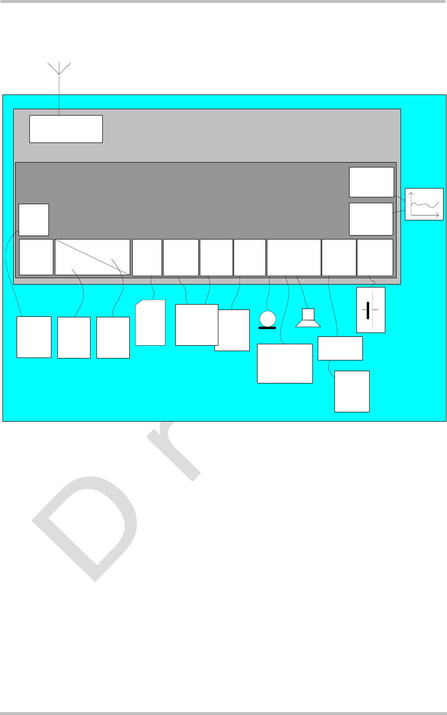
2.2 TC65 System Overview
User Application
TC65
Application Interface
Headphones
or Headset
Audio
Codec
Charger
Charging
circuit
UART
SIM card
Antenna
Interface
I
2
C
SPI
USB
DAC
ADC
Slave
USB
Host
ASC0
(Modem)
ASC1
SIM Analog
Audio
Digital
Audio Charge Power
Supply
I
2
C
Slave
SPI
10 x
GPIO
Figure 1: TC65 system overview
TC65 Hardware Interface Description
Strictly confidential / Draft s
TC65_HD_V00.450 Page 20 of 96 20.04.2005
2.3 Circuit Concept
Figure 2 shows a block diagram of the TC65 module and illustrates the major functional
components:
Baseband block:
• Digital baseband processor with DSP
• Analog processor with power supply unit (PSU)
• Flash / SRAM (stacked)
• Application interface (board-to-board connector)
RF section:
• RF transceiver
• RF power amplifier
• RF front end
• Antenna connector
Digital Baseband
Processor with DSP
Analog Controller
wit h PSU
BATT+
GND
IGT
EM ERG_ RS T
ASC(0)
5
SIM Interface
CCIN
CCRST
CCIO
CCCLK
CCVCC
D(0:15)
A(0 :24)
RD; WR; CS; WAIT
RF Control Bus
Interface
RF - Baseband
NTC
BATT_TEMP
VDDL P
SYNC
RF Part
Transce iver
RF Power
Amplifier
SRAM
Flash
6
8
TC65
Application Interface (80 pins)
I / Q
4
Au di o a na log
10
USB
3
I2C
2
VEX T
ISENSE
VSE NSE
VCHA RGE
CHARGEGATE
3
RESET
Reset
BATTYPE
TE M P2
REFCHG
ASC (1)
4
26 MHz
Front End
DAI
7
PWR _IN D
Measuring
Network
32 .76 8kH z
26 MHz
RTC
Figure 2: TC65 block diagram

TC65 Hardware Interface Description
Strictly confidential / Draft s
TC65_HD_V00.450 Page 21 of 96 20.04.2005
3 Application Interface
TC65 is equipped with an 80-pin board-to-board connector that connects to the external
application. The host interface incorporates several sub-interfaces described in the following
chapters:
• Power supply - see Section 3.1
• Charger interface – see Section 3.5
• SIM interface - see Section 3.8
• Serial interface ASC0 - see Section 3.9
• Serial interface ASC1 - see Section 3.10
• Serial interface USB - see Section 3.11
• Serial interface I²C - see Section 3.12
• Two analog audio interfaces - see Section 3.13
• Digital audio interface (DAI) - see Section 3.13 and 3.13.4
• Status and control lines: IGT, EMERG_RST, PWR_IND, SYNC - see Table 17
TC65 Hardware Interface Description
Strictly confidential / Draft s
TC65_HD_V00.450 Page 22 of 96 20.04.2005
3.1 Operating Modes
The table below briefly summarizes the various operating modes referred to in the following
chapters.
Table 1: Overview of operating modes
GSM / GPRS SLEEP Various power save modes set with AT+CFUN
command.
Software is active to minimum extent. If the module was
registered to the GSM network in IDLE mode, it is
registered and paging with the BTS in SLEEP mode,
too. Power saving can be chosen at different levels:
The NON-CYCLIC SLEEP mode (AT+CFUN=0)
disables the AT interface. The CYCLIC SLEEP modes
AT+CFUN=7 and 9 alternatively activate and deactivate
the AT interfaces to allow permanent access to all AT
commands.
GSM IDLE Software is active. Once registered to the GSM
network, paging with BTS is carried out. The module is
ready to send and receive.
GSM TALK Connection between two subscribers is in progress.
Power consumption depends on network coverage
individual settings, such as DTX off/on, FR/EFR/HR,
hopping sequences, antenna.
GPRS IDLE
EGPRS IDLE
Module is ready for GPRS/EGPRS data transfer, but no
data is currently sent or received. Power consumption
depends on network settings and GPRS/EGPRS
configuration (e.g. multislot settings).
Normal operation
GPRS DATA
EGPRS DATA
GPRS/EGPRS data transfer in progress. Power
consumption depends on network settings (e.g. power
control level), uplink / downlink data rates,
GPRS/EGPRS configuration (e.g. used multislot
settings) and reduction of maximum output power.
POWER DOWN Normal shutdown after sending the AT^SMSO command.
The Power Supply disconnects the supply voltage from the baseband part of
the circuit. Only a voltage regulator is active for powering the RTC. Software is
not active. Interfaces are not accessible.
Operating voltage (connected to BATT+) remains applied.

TC65 Hardware Interface Description
Strictly confidential / Draft s
TC65_HD_V00.450 Page 23 of 96 20.04.2005
Airplane mode Airplane mode shuts down the radio part of the module, causes the module to
log off from the GSM/GPRS network and disables all AT commands whose
execution requires a radio connection.
Airplane mode can be controlled by using the AT commands AT^SCFG and
AT+CALA:
• With AT^SCFG=MEopMode/Airplane/OnStart the module can be configured
to enter the Airplane mode each time when switched on or reset.
• The parameter AT^SCFG=MEopMode/Airplane can be used to switch back
and forth between Normal mode and Airplane mode any time during
operation.
• Setting an alarm time with AT+CALA followed by AT^SMSO wakes the
module up into Airplane mode at the scheduled time.
Charge-only mode Limited operation for battery powered applications. Enables charging while
module is detached from GSM network. Limited number of AT commands is
accessible. Charge-only mode applies when the charger is connected if the
module was powered down with AT^SMSO.
Charge mode
during normal
operation
Normal operation (SLEEP, IDLE, TALK, GPRS IDLE, GPRS/EGPRS DATA)
and charging running in parallel. Charge mode changes to Charge-only mode
when the module is powered down before charging has been completed.
See Table 6 for the various options proceeding from one mode to another.

TC65 Hardware Interface Description
Strictly confidential / Draft s
TC65_HD_V00.450 Page 24 of 96 20.04.2005
3.2 Power Supply
TC65 needs to be connected to a power supply at the B2B connector (5 pins each BATT+
and GND).
The power supply of TC65 has to be a single voltage source at BATT+. It must be able to
provide the peak current during the uplink transmission.
All the key functions for supplying power to the device are handled by the power
management section of the analog controller. This IC provides the following features:
• Stabilizes the supply voltages for the GSM baseband using low drop linear voltage
regulators.
• Switches the module's power voltages for the power up and down procedures.
• Delivers, across the VEXT pin, a regulated voltage for an external application. This
voltage is not available in Power-down mode.
• SIM switch to provide SIM power supply.
3.2.1 Minimizing Power Losses
When designing the power supply for your application please pay specific attention to power
losses. Ensure that the input voltage VBATT+ never drops below 3.2V on the TC65 board, not
even in a transmit burst where current consumption can rise to typical peaks of 2A. It should
be noted that TC65 switches off when exceeding these limits. Any voltage drops that may
occur in a transmit burst should not exceed 400mV.
The measurement network monitors outburst and inburst values. The drop is the difference
of both values. The maximum drop (Dmax) since the last start of the module will be saved. In
IDLE and SLEEP mode, the module switches off if the minimum battery voltage (Vbattmin) is
reached.
Example:
VImin = 3.2V
Dmax = 0.35V
Vbattmin = VImin + Dmax
Vbattmin = 3.2V + 0.35V = 3.55V
The best approach to reducing voltage drops is to use a board-to-board connection as
recommended, and a low impedance power source. The resistance of the power supply lines
on the host board and of a battery pack should also be considered.
Note: If the application design requires an adapter cable between both board-to-board
connectors, use a flex cable as short as possible in order to minimize power
losses.
TC65 Hardware Interface Description
Strictly confidential / Draft s
TC65_HD_V00.450 Page 25 of 96 20.04.2005
Example: If the length of the flex cable reaches the maximum length of 100mm, this
connection may cause, for example, a resistance of 30m in the BATT+ line and
30m in the GND line. As a result, a 2A transmit burst would add up to a total
voltage drop of 120mV. Plus, if a battery pack is involved, further losses may
occur due to the resistance across the battery lines and the internal resistance of
the battery including its protection circuit.
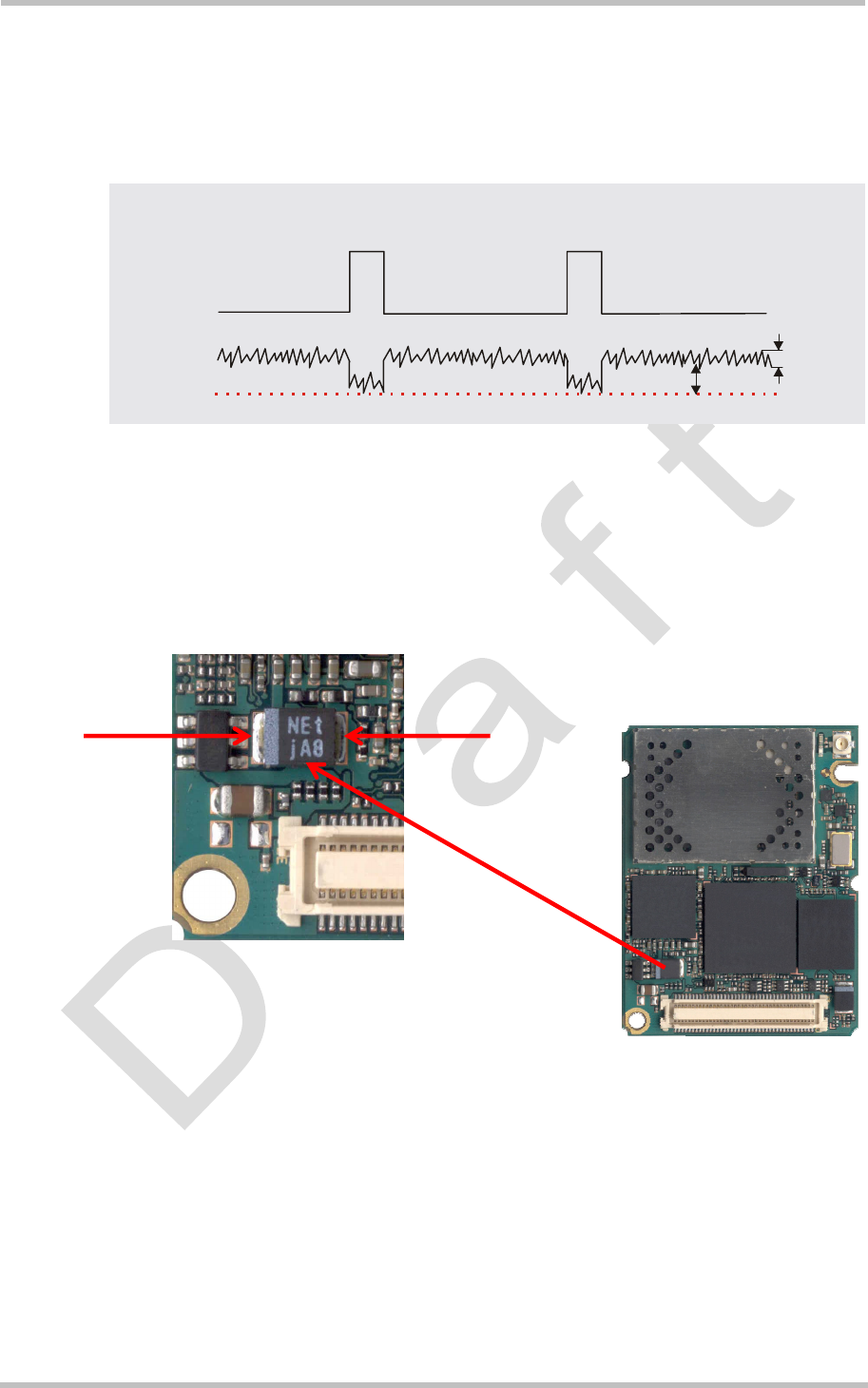
Figure 3: Power supply limits during transmit burst
3.2.2 Measuring the Supply Voltage VBATT+
The reference points for measuring the supply voltage VBATT+ on the module are BATT+ and
GND, both accessible at a capacitor located close to the board-to-board connector of the
module.
Figure 4: Position of the reference points BATT+ and GND
3.2.3 Monitoring Power Supply by AT Command
To monitor the supply voltage you can also use the AT^SBV command which returns the
value related to the reference points BATT+ and GND.
The module continuously measures the voltage at intervals depending on the operating
mode of the RF interface. The duration of measuring ranges from 0.5s in TALK/DATA mode
to 50s when TC65 is in IDLE mode or Limited Service (deregistered). The displayed voltage
(in mV) is averaged over the last measuring period before the AT^SBV command was
executed.
Transmit
burst 2A
Transmit
burst 2A
Ripple
Drop
min. 3.2V
BATT+
Reference
point
BATT+
Reference
point GND

TC65 Hardware Interface Description
Strictly confidential / Draft s
TC65_HD_V00.450 Page 26 of 96 20.04.2005
3.3 Power Up / Power Down Scenarios
In general, be sure not to turn on TC65 while it is beyond the safety limits of voltage and
temperature stated in Chapter 5. TC65 would immediately switch off after having started and
detected these inappropriate conditions. In extreme cases this can cause permanent
damage to the module.
3.3.1 Turn on TC65
TC65 can be started in a variety of ways as described in the following sections:
• Hardware driven start-up by IGT line: starts Normal mode or Airplane mode (see Section
3.3.1.1)
• Software controlled reset by AT+CFUN command: starts Normal mode or Airplane mode
(see Section 3.3.1.3)
• Hardware driven start-up by VCHARGE line: starts charging algorithm and charge-only
mode (see Section 3.3.1.2)
• Wake-up from Power-down mode by using RTC interrupt: starts Airplane mode
The option whether to start into Normal mode or Airplane mode depends on the settings
made with the AT^SCFG command or AT+CALA. With AT+CALA, followed by AT^SMSO the
module can be configured to restart into Airplane mode at a scheduled alarm time. Switching
back and forth between Normal mode and Airplane mode is possible any time during
operation by using the AT^SCFG command.
After startup or mode change the following URCs indicate the module’s ready state:
• “SYSSTART” indicates that the module has entered Normal mode.
• “^SYSSTART AIRPLANE MODE” indicates that the module has entered Airplane mode.
• “^SYSSTART CHARGE ONLY MODE” indicates that the module has entered the
Charge-only mode.
Detailed explanations on AT^SCFG, AT+CFUN, AT+CALA and Airplane mode can be found
in [1].
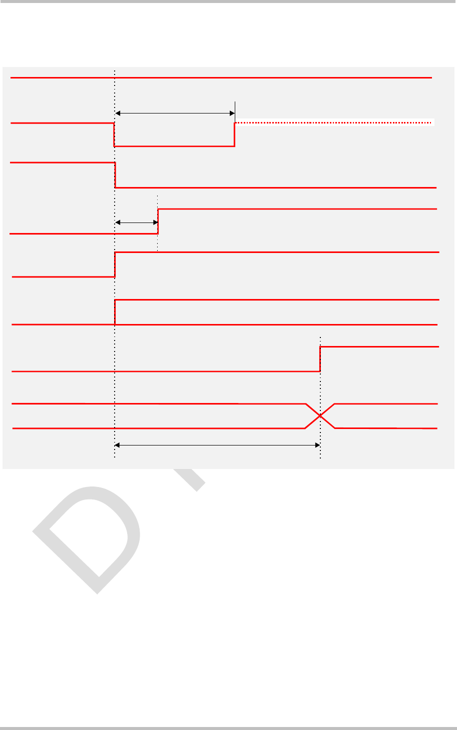
3.3.1.1 Turn on TC65 Using Ignition Line IGT
When the TC65 module is in Power-down mode, it can be started to Normal mode or
Airplane mode by driving the IGT (ignition) line to ground. This must be accomplished with an
open drain/collector driver to avoid current flowing into this pin.
The module will start up when both of the following two conditions are met:
• The supply voltage applied at BATT+ must be in the operating range.
• The IGT line needs to be driven low for at least 400ms.
Considering different strategies of host application design the figures below show two
approaches to meet this requirement: The example in Figure 5 assumes that IGT is activated
after BATT+ has already been applied. The example in Figure 6 assumes that IGT is held
low before BATT+ is switched on. In either case, to power on the module, ensure that low
state of IGT takes at least 400ms from the moment the voltage at BATT+ is available.
TC65 Hardware Interface Description
Strictly confidential / Draft s
TC65_HD_V00.450 Page 27 of 96 20.04.2005
If configured to a fix baud rate (AT+IPR0), the module will send the URC “^SYSSTART” or
“^SYSSTART AIRPLANE MODE” to notify that it is ready to operate. If autobauding is
enabled (AT+IPR=0) there will be no notification.
EMERG_RST
VEXT
TXD0/TXD1/RTS0/RST1/DTR0 (driven by the application)
CTS0/CTS1/DSR0/DCD0
ca. 500 ms
Serial interfaces
ASC0 and ASC1
Undefined Active
PWR_IND
t = 400ms
min
120ms
BATT+
IGT
HiZ
Figure 5: Power-on with operating voltage at BATT+ applied before activating IGT
TC65 Hardware Interface Description
Strictly confidential / Draft s
TC65_HD_V00.450 Page 28 of 96 20.04.2005
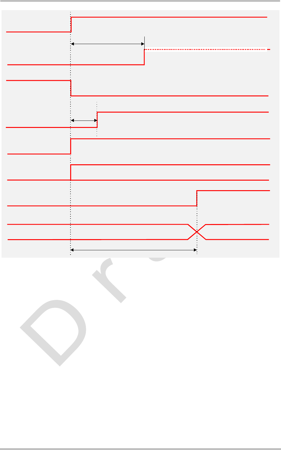
EMERG_RST
PWR_IND
t = 400ms
min
120ms
BATT+
IGT
HiZ
VEXT
TXD0/TXD1/RTS0/RST1/DTR0 (driven by the application)
CTS0/CTS1/DSR0/DCD0
ca. 500 ms
Serial interfaces
ASC0 and ASC1
Undefined Active
Figure 6: Power-on with IGT held low before switching on operating voltage at BATT+
3.3.1.2 Turn on TC65 Using the VCHARGE Signal
As detailed in Section 3.5.7, the charging adapter can be connected regardless of the
module’s operating mode.
If the charger is connected to the charger input of the external charging circuit and the
module’s VCHARGE pin while TC65 is off, and the battery voltage is above the undervoltage
lockout threshold, processor controlled fast charging starts (see Section 3.5.6). TC65 enters
a restricted mode, referred to as Charge-only mode where only the charging algorithm will be
launched.
During the Charge-only mode TC65 is neither logged on to the GSM network nor are the
serial interfaces fully accessible. To switch to normal operation and log on to the GSM
network, the IGT line needs to be activated as described in Section 3.3.1.

TC65 Hardware Interface Description
Strictly confidential / Draft s
TC65_HD_V00.450 Page 29 of 96 20.04.2005
3.3.1.3 Reset TC65 via AT+CFUN Command
To reset and restart the TC65 module use the command AT+CFUN. You can enter
AT+CFUN=,1 or AT+CFUN=x,1, where x may be in the range from 0 to 9. See [1] for details.
If configured to a fix baud rate (AT+IPR0), the module will send the URC “^SYSSTART” or
“^SYSSTART AIRPLANE MODE” to notify that it is ready to operate. If autobauding is
enabled (AT+IPR=0) there will be no notification. To register to the network SIM PIN
authentication is necessary after restart.
3.3.1.4 Reset TC65 in Case of Emergency via EMERG_RST
Caution: Use the EMERG_RST pin only when, due to serious problems, the software is not
responding for more than 5 seconds. Pulling the EMERG_RST pin causes the loss of all
information stored in the volatile memory since the processor restarts immediately.
Therefore, this procedure is intended only for use in case of emergency, e.g. if TC65 does
not respond, if reset or shutdown via AT command fails.
The EMERG_RST signal is available on the application interface. To control the
EMERG_RST line it is recommended to use an open drain / collector driver.
To actually reset the TC65 module, the EMERG_RST line must be pulled to ground for
≥10ms. After releasing the line TC65 will start again.
After hardware driven restart, notification via “^SYSSTART” or “^SYSSTART AIRPLANE”
URC is the same as in case of restart by IGT or AT command. To register to the network SIM
PIN authentication is necessary after restart.

TC65 Hardware Interface Description
Strictly confidential / Draft s
TC65_HD_V00.450 Page 30 of 96 20.04.2005
3.3.2 Turn off TC65
TC65 can be turned off as follows:
• Normal shutdown: Software controlled by AT^SMSO command
• Automatic shutdown: Takes effect if board or battery temperature is out of range or if
undervoltage or overvoltage conditions occur.
3.3.2.1 Turn off TC65 Using AT Command
The best and safest approach to powering down TC65 is to issue the AT^SMSO command.
This procedure lets TC65 log off from the network and allows the software to enter into a
secure state and safe data before disconnecting the power supply. The mode is referred to
as Power-down mode. In this mode, only the RTC stays active.
Before switching off the device sends the following response:
^SMSO: MS OFF
OK
^SHUTDOWN
After sending AT^SMSO do not enter any other AT commands. There are two ways to verify
when the module turns off:
• Wait for the URC “^SHUTDOWN”. It indicates that data have been stored non-volatile
and the module turns off in less than 1 second.
• Also, you can monitor the PWR_IND pin. High state of PWR_IND definitely indicates that
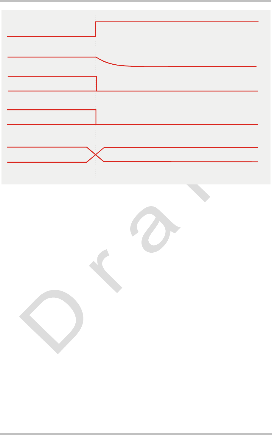
the module is switched off.
Be sure not to disconnect the supply voltage VBATT+ before the URC “^SHUTDOWN” has
been issued and the PWR_IND signal has gone high. Otherwise you run the risk of losing
data. Signal states during turn-off are shown in Figure 7.
While TC65 is in Power-down mode the application interface is switched off and must not be
fed from any other source. Therefore, your application must be designed to avoid any current
flow into any digital pins of the application interface, especially of the serial interfaces. No
special care is required for the USB interface which is protected from reverse current.
TC65 Hardware Interface Description
Strictly confidential / Draft s
TC65_HD_V00.450 Page 31 of 96 20.04.2005
VEXT See note 1
TXD0/TXD1/RTS0/RTS1/DTR0 (driven by the application)
Serial interfaces
ASC0 and ASC1
Undefined
Active
PWR_IND
CTS0/CTS1/DSR0/DTR0
Figure 7: Signal states during turn-off procedure
Note 1: Depending on capacitance load from host application
3.3.2.2 Leakage Current in Power Down Mode
The leakage current in Power Down mode varies depending on the following conditions:
• If the supply voltage at BATT+ was disconnected and then applied again without starting
up the TC65 module, the leakage current ranges between 90µA and 100µA.
• If the TC65 module is started and afterwards powered down with AT^SMSO, then the
leakage current is only 50µA.
Therefore, in order to minimize the leakage current take care to start up the module at least
once before it is powered down.

TC65 Hardware Interface Description
Strictly confidential / Draft s
TC65_HD_V00.450 Page 32 of 96 20.04.2005
3.3.3 Automatic Shutdown
Automatic shutdown takes effect if:
• the TC65 board is exceeding the critical limits of overtemperature or undertemperature
• the battery is exceeding the critical limits of overtemperature or undertemperature
• undervoltage or overvoltage is detected
See Charge-only mode described in section 3.5.7 for exceptions.
The automatic shutdown procedure is equivalent to the Power-down initiated with the
AT^SMSO command, i.e. TC65 logs off from the network and the software enters a secure
state avoiding loss of data.
Alert messages transmitted before the device switches off are implemented as Unsolicited
Result Codes (URCs). The presentation of these URCs can be enabled or disabled with the
two AT commands AT^SBC and AT^SCTM. The URC presentation mode varies with the
condition, please see Chapters 3.3.3.1 to 3.3.3.4 for details. For further instructions on AT
commands refer to [1].
3.3.3.1 Temperature Dependent Shutdown
The board temperature is constantly monitored by an internal NTC resistor located on the
PCB. The NTC that detects the battery temperature must be part of the battery pack circuit
as described in 3.5.3 The values detected by either NTC resistor are measured directly on
the board or the battery and therefore, are not fully identical with the ambient temperature.
Each time the board or battery temperature goes out of range or back to normal, TC65
instantly displays an alert (if enabled).
• URCs indicating the level "1" or "-1" allow the user to take appropriate precautions, such
as protecting the module from exposure to extreme conditions. The presentation of the
URCs depends on the settings selected with the AT^SCTM write command:
AT^SCTM=1: Presentation of URCs is always enabled.
AT^SCTM=0 (default): Presentation of URCs is enabled for 15 seconds time after
start-up of TC65. After 15 seconds operation, the presentation will be disabled, i.e. no
alert messages can be generated.
• URCs indicating the level "2" or "-2" are instantly followed by an orderly shutdown. The
presentation of these URCs is always enabled, i.e. they will be output even though the
factory setting AT^SCTM=0 was never changed.
The maximum temperature ratings are stated in Table 16. Refer to Table 2 for the associated
URCs. All statements are based on test conditions according to IEC 60068-2-2 (still air).

TC65 Hardware Interface Description
Strictly confidential / Draft s
TC65_HD_V00.450 Page 33 of 96 20.04.2005
Table 2: Temperature dependent behavior
Sending temperature alert (15s after TC65 start-up, otherwise only if URC presentation enabled)
^SCTM_A: 1 Caution: Tamb of battery close to overtemperature limit.
^SCTM_B: 1 Caution: Tamb of board close to overtemperature limit.
^SCTM_A: -1 Caution: Tamb of battery close to undertemperature limit.
^SCTM_B: -1 Caution: Tamb of board close to undertemperature limit.
^SCTM_A: 0 Battery back to uncritical temperature range.
^SCTM_B: 0 Board back to uncritical temperature range.
Automatic shutdown (URC appears no matter whether or not presentation was enabled)
^SCTM_A: 2 Alert: Tamb of battery equal or beyond overtemperature limit. TC65 switches off.
^SCTM_B: 2 Alert: Tamb of board equal or beyond overtemperature limit. TC65 switches off.
^SCTM_A: -2 Alert: Tamb of battery equal or below undertemperature limit. TC65 switches off.
^SCTM_B: -2 Alert: Tamb of board equal or below undertemperature limit. TC65 switches off.
3.3.3.2 Temperature Control during Emergency call
If the temperature limit is exceeded while an emergency call is in progress the engine
continues to measure the temperature, but deactivates the shutdown functionality. If the
temperature is still out of range when the call ends, the module switches off immediately
(without another alert message).
3.3.3.3 Undervoltage Shutdown if Battery NTC is Present
In applications where the module’s charging technique is used and an NTC is connected to
the BATT_TEMP terminal, the software constantly monitors the applied voltage. If the
measured battery voltage is no more sufficient to set up a call the following URC will be
presented:
^SBC: Undervoltage.
The message will be reported, for example, when you attempt to make a call while the
voltage is close to the shutdown threshold of 3.2V and further power loss is caused during
the transmit burst. In IDLE mode, the shutdown threshold is the sum of the module’s
minimum supply voltage (3.2V) and the value of the maximum voltage drop resulting from
earlier calls. This means that in IDLE mode the actual shutdown threshold may be higher
than 3.2V. Therefore, to properly calculate the actual shutdown threshold application
manufacturers are advised to measure the maximum voltage drops that may occur during
transmit bursts.
To remind you that the battery needs to be charged soon, the URC appears several times
before the module switches off.
To enable or disable the URC use the AT^SBC command. The URC will be enabled when
you enter the write command and specify the current consumption of your host application.
Step by step instructions are provided in [1].

TC65 Hardware Interface Description
Strictly confidential / Draft s
TC65_HD_V00.450 Page 34 of 96 20.04.2005
3.3.3.4 Undervoltage Shutdown if no Battery NTC is Present
The undervoltage protection is also effective in applications, where no NTC connects to the
BATT_TEMP terminal. Thus, you can take advantage of this feature even though the
application handles the charging process or TC65 is fed by a fixed supply voltage. All you
need to do is executing the write command AT^SBC=<current> which automatically enables
the presentation of URCs. You do not need to specify <current>.
Whenever the supply voltage falls below the value of 3.2V the URC
^SBC: Undervoltage
appears several times before the module switches off.
3.3.3.5 Overvoltage Shutdown
In the event of the maximum voltage of 4.6V is reached the module sends a URC and then
performs an orderly shutdown. Further details: TBD
Keep in mind that several TC65 components are directly linked to BATT+ and, therefore, the
supply voltage remains applied at major parts of TC65, even if the module is switched off.
Especially the power amplifier is very sensitive to high voltage and might even be destroyed.

TC65 Hardware Interface Description
Strictly confidential / Draft s
TC65_HD_V00.450 Page 35 of 96 20.04.2005
3.4 Automatic GPRS Multislot Class Change
Temperature control is also effective for operation in GPRS Multislot Class 10 and GPRS
Multislot Class 12. If the board temperature increases to the limit specified for restricted
operation1) while data are transmitted over GPRS, the module automatically reverts:
• from GPRS Multislot Class 12 (4Tx slots) to GPRS Multislot Class 8 (1Tx),
• from GPRS Multislot Class 10 (2Tx slots) to GPRS Multislot Class 8 (1Tx)
This reduces the power consumption and, consequently, causes the board’s temperature to
decrease. Once the temperature drops to a value of 5 degrees below the limit of restricted
operation, TC65 returns to the higher Multislot Class. If the temperature stays at the critical
level or even continues to rise, TC65 will not switch back to the higher class.
After a transition from GPRS Multislot Class 12 or 10 to GPRS Multislot Class 8 a possible
switchback to GPRS Multislot Class 12 or 10 is blocked for one minute.
Please note that there is not one single cause of switching over to a lower Multislot Class.
Rather it is the result of an interaction of several factors, such as the board temperature that
depends largely on the ambient temperature, the operating mode and the transmit power.
Furthermore, take into account that there is a delay until the network proceeds to a lower or,
accordingly, higher Multislot Class. The delay time is network dependent. In extreme cases,
if it takes too much time for the network and the temperature cannot drop due to this delay,
the module may even switch off as described in Section 3.3.3.1.
1) See Table 16 for temperature limits known as restricted operation.

TC65 Hardware Interface Description
Strictly confidential / Draft s
TC65_HD_V00.450 Page 36 of 96 20.04.2005
3.5 Charging Control
TC65 integrates a charging management for rechargeable Lithium Ion and Lithium Polymer
batteries. You can skip this chapter if charging is not your concern, or if you are not using the
implemented charging algorithm.
The following sections contain an overview of charging and battery specifications. Please
refer to [4] for greater detail, especially regarding requirements for batteries and chargers,
appropriate charging circuits, recommended batteries and an analysis of operational issues
typical of battery powered GSM/GPRS applications.
3.5.1 Hardware Requirements
TC65 has no on-board charging circuit. To benefit from the implemented charging
management you are required to install a charging circuit within your application according to
the Figure 38.
3.5.2 Software Requirements
Use the command AT^SBC, parameter <current>, to enter the current consumption of the
host application. This information enables the TC65 module to correctly determine the end of
charging and terminate charging automatically when the battery is fully charged. If the
<current> value is inaccurate and the application draws a current higher than the final charge
current, either charging will not be terminated or the battery fails to reach its maximum
voltage. Therefore, the termination condition is defined as: final charge current (50mA) plus
current consumption of the external application. If used the current flowing over the VEXT pin
of the application interface (typically 2.9V) must be added, too.
The parameter <current> is volatile, meaning that the factory default (0mA) is restored each
time the module is powered down or reset. Therefore, for better control of charging, it is
recommended to enter the value every time the module is started.
See [1] for details on AT^SBC.
TC65 Hardware Interface Description
Strictly confidential / Draft s
TC65_HD_V00.450 Page 37 of 96 20.04.2005
3.5.3 Battery Pack Requirements
The charging algorithm has been optimized for rechargeable Lithium batteries that meet the
characteristics listed below and in Table 3. It is recommended that the battery pack you want
to integrate into your TC65 application is compliant with these specifications. This ensures
reliable operation, proper charging and, particularly, allows you to monitor the battery
capacity using the AT^SBC command. Failure to comply with these specifications might
cause AT^SBC to deliver incorrect battery capacity values.
• Li-Ion or Lithium Polymer battery pack specified for a maximum charging voltage of 4.2V
and a recommended capacity of 1000 to 1200mAh.
• Since charging and discharging largely depend on the battery temperature, the battery
pack should include an NTC resistor. If the NTC is not inside the battery it must be in
thermal contact with the battery. The NTC resistor must be connected between
BATT_TEMP and GND.
The B value of the NTC should be in the range: 10kΩ +5% @ 25°C, B25/85 = 3423K to B
=3435K ± 3% (alternatively acceptable: 10kΩ +2% @ 25°C, B25/50 = 3370K +3%). Please
note that the NTC is indispensable for proper charging, i.e. the charging process will not
start if no NTC is present.
• Ensure that the pack incorporates a protection circuit capable of detecting overvoltage
(protection against overcharging), undervoltage (protection against deep discharging)
and overcurrent. Due to the discharge current profile typical of GSM applications, the
circuit must be insensitive to pulsed current.
• On the TC65 module, a built-in measuring circuit constantly monitors the supply voltage.
In the event of undervoltage, it causes TC65 to power down. Undervoltage thresholds are
specific to the battery pack and must be evaluated for the intended model. When you
evaluate undervoltage thresholds, consider both the current consumption of TC65 and of
the application circuit.
• The internal resistance of the battery and the protection should be as low as possible. It
is recommended not to exceed 150m, even in extreme conditions at low temperature.
The battery cell must be insensitive to rupture, fire and gassing under extreme conditions
of temperature and charging (voltage, current).
• The battery pack must be protected from reverse pole connection. For example, the
casing should be designed to prevent the user from mounting the battery in reverse
orientation.
• It is recommended that the battery pack be approved to satisfy the requirements of CE
conformity.
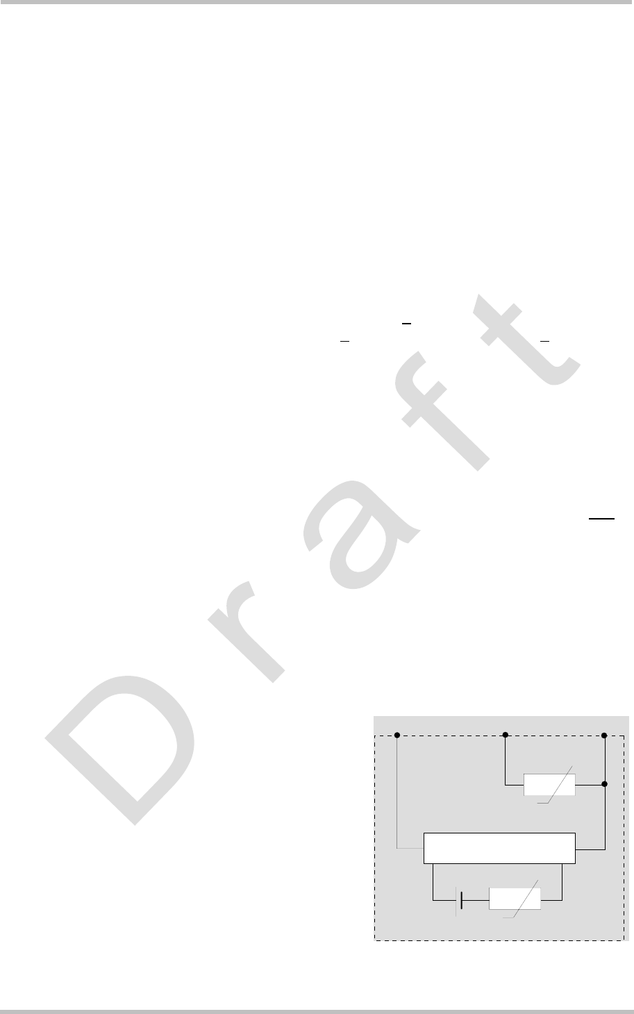
Figure 8 shows the circuit diagram of a typical
battery pack design that includes the protection
elements described above.
Figure 8: Battery pack circuit diagram
to BATT_TEMP to GND
NTC
Polyfuse
ϑ
Protection Circuit
+-
Battery cell
to BATT+

TC65 Hardware Interface Description
Strictly confidential / Draft s
TC65_HD_V00.450 Page 38 of 96 20.04.2005
Table 3: Specifications of battery packs suitable for use with TC65
Battery type Rechargeable Lithium Ion or Lithium Polymer battery
Nominal voltage 3.6V / 3.7V
Capacity Recommended: 1000mAh to 1200mAh
Minimum: 500mAh
NTC 10k ± 5% @ 25°C
approx. 5k @ 45°C
approx. 26.2k @ 0°C
B value range: B (25/85)=3423K to B =3435K ± 3%
Overcharge detection voltage 4.325 ± 0.025V
Overdischarge detection voltage 2.5 ± 0.05V
Overcurrent detection 3 ± 0.5A
Overcurrent detection delay time 4 ~ 16ms
Short detection delay time 50µs
Internal resistance <130m
Note: A maximum internal resistance of 150m should not
be exceeded even after 500 cycles and under extreme
conditions.
3.5.4 Batteries Recommended for Use with TC65
When you choose a battery for your TC65 application you can take advantage of one of the
following two batteries offered by VARTA Microbattery GmbH. Both batteries meet all
requirements listed above. They have been thoroughly tested by Siemens, proved to be
suited for TC65, and are CE approved.
• LIP 633450A1B PCM.STB, type Lithium Ion
This battery is listed in the standard product range of VARTA. It is incorporated in a
shrink sleeve and has been chosen for integration into the reference setup submitted for
Type Approval of Siemens GSM modules.
• LPP 503759CA PCM.NTC.LT50, type Lithium Polymer
This battery has been especially designed by VARTA for use with Siemens GSM
modules. It has the same properties as the above Li-Ion battery, except that it is type
Polymer, is smaller and comes without casing.
Specifications, construction drawings and sales contacts for both VARTA batteries can be
found in Section 9.3.

TC65 Hardware Interface Description
Strictly confidential / Draft s
TC65_HD_V00.450 Page 39 of 96 20.04.2005
3.5.5 Charger Requirements
For using the implemented charging algorithm and the reference charging circuit
recommended in [4] and in Figure 38, the charger has to meet the following requirements:
Output voltage: 5.2Volts ±0.2V (stabilized voltage)
Output current: 500mA
Chargers with a higher output current are acceptable, but please
consider that only 500mA will be applied when a 0.3Ohms shunt
resistor is connected between VSENSE and ISENSE. See [4] for
further details.
3.5.6 Implemented Charging Technique
If all requirements listed above are met (appropriate external charging circuit of application,
battery pack, charger, AT^SBC settings) then charging is enabled in various stages
depending on the battery condition:
Trickle charging:
• Trickle charge current flows over the VCHARGE line.
• Trickle charging is done when a charger is present (connected to VCHARGE) and the
battery is deeply discharged or has undervoltage. If deeply discharged (Deep Discharge
Lockout at VBATT+= 0…2.5V) the battery is charged with 5mA, in case of undervoltage
(Undervoltage Lockout at VBATT+= 2.5…3.2V) it is charged with 30mA
Software controlled charging:
• Controlled over the CHARGEGATE.
• Temperature conditions: 0°C to 45°C
• Software controlled charging is done when the charger is present (connected to
VCHARGE) and the battery voltage is at least above the undervoltage threshold.
Software controlled charging passes the following stages:
- Power ramp: Depending on the discharge level of the battery (i.e. the measured battery
voltage VBATT+) the software adjusts the maximum charge current for charging the
battery. The duration of power ramp charging is very short (less than 30 seconds).
- Fast charging: Battery is charged with constant current (approx. 500mA) until the
battery voltage reaches 4.2V (approx. 80% of the battery capacity).
- Top-up charging: The battery is charged with constant voltage of 4.2V at stepwise
reducing charge current until full battery capacity is reached.
• The duration of software controlled charging depends on the battery capacity and the
level of discharge.

TC65 Hardware Interface Description
Strictly confidential / Draft s
TC65_HD_V00.450 Page 40 of 96 20.04.2005
3.5.7 Operating Modes during Charging
Of course, the battery can be charged regardless of the engine's operating mode. When the
GSM module is in Normal mode (SLEEP, IDLE, TALK, GPRS IDLE or GPRS DATA mode), it
remains operational while charging is in progress (provided that sufficient voltage is applied).
The charging process during the Normal mode is referred to as Charge mode.
If the charger is connected to the charger input of the external charging circuit and the
module’s VCHARGE pin while TC65 is in Power-down mode, TC65 goes into Charge-only
mode.
While the charger remains connected it is not possible to switch the module off by using the
AT^SMSO command or the automatic shutdown mechanism. Instead the following applies:
• If the module is in Normal mode and the charger is connected (Charge mode) the
AT^SMSO command causes the module to shut down shortly and then start into the
Charge-only mode.
• In Charge-only mode the AT^SMSO command is not usable.
• In Charge-only mode the module neither switches off when the battery or the module
exceeds the critical limits of overtemperature or undertemperature.
In these cases you can only switch the module off by disconnecting the charger.
To proceed from Charge-only mode to another operating mode you have the following
options:
• To switch from Charge-only mode to Normal mode drive the ignition line (IGT) to ground
for 1 second.
• To switch from Charge-only mode to Airplane mode enter the command
AT^SCFG=MEopMode/Airplane,on.
• If
AT^SCFG=MEopMode/Airplane/OnStart,on is set, driving the ignition line (IGT)
activates the Airplane mode.
TC65 Hardware Interface Description
Strictly confidential / Draft s
TC65_HD_V00.450 Page 41 of 96 20.04.2005
Table 4: Comparison Charge-only and Charge mode
How to activate mode
Description of mode
Charge mode
Connect charger to charger input of host
application charging circuit and module’s
VCHARGE pin while TC65 is
• operating, e.g. in IDLE or TALK mode
• in SLEEP mode
• Battery can be charged while GSM module
remains operational and registered to the
GSM network.
• In IDLE and TALK mode, the serial interfaces
are accessible. All AT commands can be
used to full extent.
NOTE: If the module operates at maximum
power level (PCL5) and GPRS Class 12 at the
same time the current consumption is higher than
the current supplied by the charger.
Charge-only mode
Connect charger to charger input of host
application charging circuit and module’s
VCHARGE pin while TC65 is
• in Power-down mode
• in Normal mode: Connect charger to
the VCHARGE pin, then enter
AT^SMSO.
NOTE: While trickle charging is in
progress, be sure that the host
application is switched off. If the
application is fed from the trickle charge
current the module might be prevented
from proceeding to software controlled
charging since the current would not be
sufficient.
• Battery can be charged while GSM engine is
deregistered from GSM network.
• Charging runs smoothly due to constant
current consumption.
• The AT interface is accessible and allows to
use the commands listed below.
Table 5: AT commands available in Charge-only mode
AT command Use
AT+CALA Set alarm time, configure Airplane mode.
AT+CCLK Set date and time of RTC.
AT^SBC Query status of charger connection. Enable / disable “^SBC” URCs.
AT^SBV Monitor supply voltage.
AT^SCTM Query temperature range, enable/disable URCs to report critical temperature
ranges
AT^SCFG Enable/disable parameters MEopMode/Airplane or MEopMode/Airplane/OnStart

TC65 Hardware Interface Description
Strictly confidential / Draft s
TC65_HD_V00.450 Page 42 of 96 20.04.2005
3.6 Summary of State Transitions (Except SLEEP Mode)
Table 6: State transitions of TC65 (except SLEEP mode)
The table shows how to proceed from one mode to another (grey column = present mode, white columns = intended modes)
Further mode ÎÎÎ
Present mode
POWER DOWN Normal mode**) Charge-only mode*) Airplane mode
POWER DOWN
mode
--- If AT^SCFG=MeOpMode/
Airplane/OnStart,off:
IGT >400 ms at low level
Connect charger to VCHARGE If AT^SCFG=MeOpMode/
Airplane/OnStart,on:
IGT >400 ms at low level
Regardless of AT^SCFG
configuration: scheduled wake-up set
with AT+CALA.
Normal mode**) AT^SMSO --- AT^SMSO if charger is
connected
AT^SCFG=MeOpMode/
Airplane,on.
If AT^SCFG=MeOpMode/
Airplane/OnStart,on:
AT+CFUN=x,1
or EMERG_RST.
Charge-only mode *) Disconnect charger If AT^SCFG=MeOpMode/
Airplane/OnStart,off:
IGT >1s at low level
--- AT^SCFG=MeOpMode/
Airplane,on.
If AT^SCFG=MeOpMode/
Airplane/OnStart,on: IGT >1s at low
level
Airplane mode AT^SMSO AT^SCFG=MeOpMode/
Airplane,off
AT^SMSO if charger is
connected
---
*) See section 3.5.7 for details on the charging mode **) Normal mode covers TALK, DATA, GPRS, EGPRS, IDLE and SLEEP modes
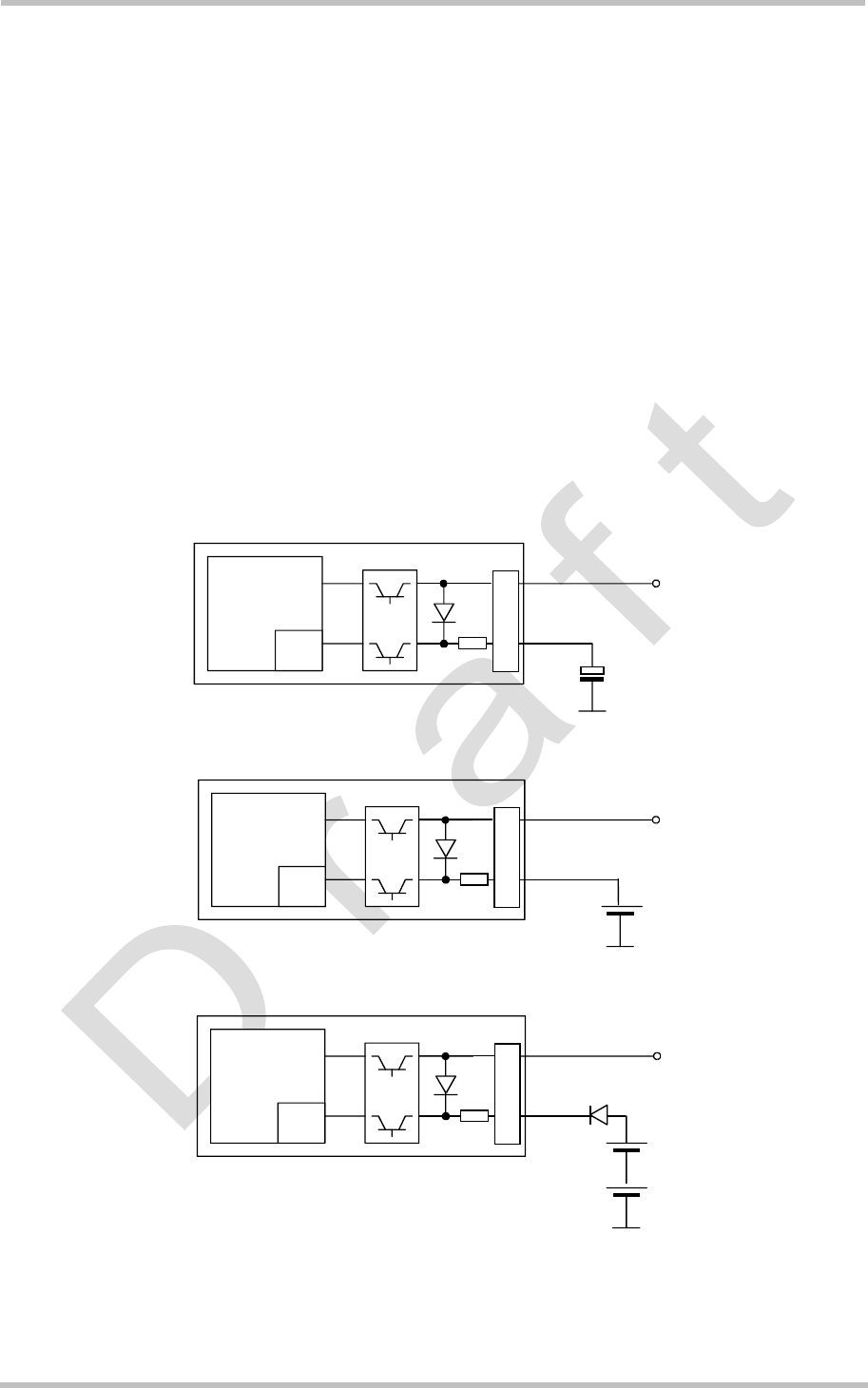
TC65 Hardware Interface Description
Strictly confidential / Draft s
TC65_HD_V00.450 Page 43 of 96 20.04.2005
3.7 RTC Backup
The internal Real Time Clock of TC65 is supplied from a separate voltage regulator in the
analog controller which is also active when TC65 is in POWER DOWN status. An alarm
function is provided that allows to wake up TC65 to Airplane mode without logging on to the
GSM network.
In addition, you can use the VDDLP pin on the board-to-board connector to backup the RTC
from an external capacitor or a battery (rechargeable or non-chargeable). The capacitor is
charged by the BATT+ line of TC65. If the voltage supply at BATT+ is disconnected the RTC
can be powered by the capacitor. The size of the capacitor determines the duration of
buffering when no voltage is applied to TC65, i.e. the larger the capacitor the longer TC65
will save the date and time.
A serial 1k resistor placed on the board next to VDDLP limits the charge current of an
empty capacitor or battery.
The following figures show various sample configurations. Please refer to Table 17 for the
parameters required.
Baseband
processor
RTC
PSU
+
BATT+
1k
B2B
VDDLP
Figure 9: RTC supply from capacitor
RTC
+
BATT+
1k
B2B
VDDLP
Baseband
processor PSU
Figure 10: RTC supply from rechargeable battery
RTC
+
+
BATT+
1k
VDDLP
B2B
Baseband
processor PSU
Figure 11: RTC supply from non-chargeable battery
TC65 Hardware Interface Description
Strictly confidential / Draft s
TC65_HD_V00.450 Page 44 of 96 20.04.2005
3.8 SIM Interface
The baseband processor has an integrated SIM interface compatible with the ISO 7816 IC
Card standard. This is wired to the host interface (board-to-board connector) in order to be
connected to an external SIM card holder. Six pins on the board-to-board connector are
reserved for the SIM interface.
The SIM interface supports 3V and 1.8V SIM cards. Please refer to Table 17 for electrical
specifications of the SIM interface lines depending on whether a 3V or 1.8V SIM card is
used.
The CCIN pin serves to detect whether a tray (with SIM card) is present in the card holder.
Using the CCIN pin is mandatory for compliance with the GSM 11.11 recommendation if the
mechanical design of the host application allows the user to remove the SIM card during
operation. To take advantage of this feature, an appropriate SIM card detect switch is
required on the card holder. For example, this is true for the model supplied by Molex, which
has been tested to operate with TC65 and is part of the Siemens reference equipment
submitted for type approval. See Chapter 8 for Molex ordering numbers.
Table 7: Signals of the SIM interface (board-to-board connector)
Signal Description
CCGND Separate ground connection for SIM card to improve EMC.
Be sure to use this ground line for the SIM interface rather than any other ground pin or
plane on the module. A design example for grounding the SIM interface is shown in
Figure 38.
CCCLK Chipcard clock, various clock rates can be set in the baseband processor.
CCVCC SIM supply voltage.
CCIO Serial data line, input and output.
CCRST Chipcard reset, provided by baseband processor.
CCIN Input on the baseband processor for detecting a SIM card tray in the holder. If the SIM is
removed during operation the SIM interface is shut down immediately to prevent
destruction of the SIM. The CCIN pin is active low.
The CCIN pin is mandatory for applications that allow the user to remove the SIM card
during operation.
The CCIN pin is solely intended for use with a SIM card. It must not be used for any other
purposes. Failure to comply with this requirement may invalidate the type approval of
TC65.
The total cable length between the board-to-board connector pins on TC65 and the pins of
the external SIM card holder must not exceed 100mm in order to meet the specifications of
3GPP TS 51.010-1 and to satisfy the requirements of EMC compliance.
To avoid possible cross-talk from the CCCLK signal to the CCIO signal be careful that both
lines are not placed closely next to each other. A useful approach is using the CCGND line to
shield the CCIO line from the CCCLK line.
Note: No guarantee can be given, nor any liability accepted, if loss of data is encountered
after removing the SIM card during operation.
Also, no guarantee can be given for properly initializing any SIM card that the user
inserts after having removed a SIM card during operation. In this case, the application
must restart TC65.
TC65 Hardware Interface Description
Strictly confidential / Draft s
TC65_HD_V00.450 Page 45 of 96 20.04.2005
3.9 Serial Interface ASC0
TC65 offers an 8-wire unbalanced, asynchronous modem interface ASC0 conforming to ITU-
T V.24 protocol DCE signalling. The electrical characteristics do not comply with ITU-T V.28.
The significant levels are 0V (for low data bit or active state) and 2.9V (for high data bit or
inactive state). For electrical characteristics please refer to Table 17.
TC65 is designed for use as a DCE. Based on the conventions for DCE-DTE connections it
communicates with the customer application (DTE) using the following signals:
• Port TXD @ application sends data to the module’s TXD0 signal line
• Port RXD @ application receives data from the module’s RXD0 signal line
GSM module (DCE) Application (DTE)
TXD
RXD
RTS
CTS
RING
DCD
DSR
DTR
TXD0
RXD0
RTS0
CTS0
RING0
DCD0
DSR0
DTR0
Figure 12: Serial interface ASC0
Features
• Includes the data lines TXD0 and RXD0, the status lines RTS0 and CTS0 and, in
addition, the modem control lines DTR0, DSR0, DCD0 and RING0.
• ASC0 is primarily designed for controlling voice calls, transferring CSD, fax and GPRS
data and for controlling the GSM engine with AT commands.
• Full Multiplex capability allows the interface to be partitioned into three virtual channels,
yet with CSD and fax services only available on the first logical channel. Please note that
when the ASC0 interface runs in Multiplex mode, ASC1 cannot be used. For more details
on Multiplex mode see [5].
• The DTR0 signal will only be polled once per second from the internal firmware of TC65.
• The RING0 signal serves to indicate incoming calls and other types of URCs (Unsolicited
Result Code). It can also be used to send pulses to the host application, for example to
wake up the application from power saving state. See [1] for details on how to configure
the RING0 line by AT^SCFG.
• By default, configured for 8 data bits, no parity and 1 stop bit. The setting can be
changed using the AT command AT+ICF and, if required, AT^STPB. For details see [1].
• ASC0 can be operated at bit rates from 300bps to 460800bps.
• Autobauding supports the following bit rates: TBD.
• Autobauding is not compatible with multiplex mode.
• Supports RTS0/CTS0 hardware flow control and XON/XOFF software flow control.

TC65 Hardware Interface Description
Strictly confidential / Draft s
TC65_HD_V00.450 Page 46 of 96 20.04.2005
Table 8: DCE-DTE wiring of ASC0
DCE DTE V.24
circuit Pin function Signal direction Pin function Signal direction
103 TXD0 Input TXD Output
104 RXD0 Output RXD Input
105 RTS0 Input RTS Output
106 CTS0 Output CTS Input
108/2 DTR0 Input DTR Output
107 DSR0 Output DSR Input
109 DCD0 Output DCD Input
125 RING0 Output /RING Input
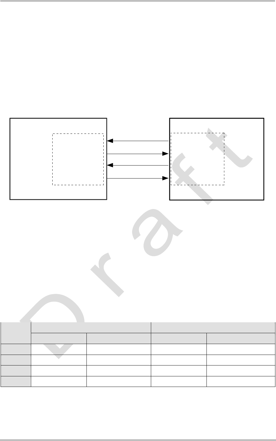
TC65 Hardware Interface Description
Strictly confidential / Draft s
TC65_HD_V00.450 Page 47 of 96 20.04.2005
3.10 Serial Interface ASC1
TC65 offers a 4-wire unbalanced, asynchronous modem interface ASC1 conforming to ITU-T
V.24 protocol DCE signalling. The electrical characteristics do not comply with ITU-T V.28.
The significant levels are 0V (for low data bit or active state) and 2.9V (for high data bit or
inactive state). For electrical characteristics please refer to Table 17.
TC65 is designed for use as a DCE. Based on the conventions for DCE-DTE connections it
communicates with the customer application (DTE) using the following signals:
• Port TXD @ application sends data to module’s TXD1 signal line
• Port RXD @ application receives data from the module’s RXD1 signal line
GSM module (DCE) Application (DTE)
TXD
RXD
RTS
CTS
TXD1
RXD1
RTS1
CTS1
Figure 13: Serial interface ASC1
Features
• Includes only the data lines TXD1 and RXD1 plus RTS1 and CTS1 for hardware
handshake.
• On ASC1 no RING line is available. The indication of URCs on the second interface
depends on the settings made with the AT^SCFG command. For details refer to [1].
• Configured for 8 data bits, no parity and 1 or 2 stop bits.
• ASC1 can be operated at bit rates from 300bps to 460800bps.
• Autobauding TBD.
• Supports RTS1/CTS1 hardware flow control and XON/XOFF software flow control.
Table 9: DCE-DTE wiring of ASC1
DCE DTE V.24
circuit Pin function Signal direction Pin function Signal direction
103 TXD1 Input TXD Output
104 RXD1 Output RXD Input
105 RTS1 Input RTS Output
106 CTS1 Output CTS Input
TC65 Hardware Interface Description
Strictly confidential / Draft s
TC65_HD_V00.450 Page 48 of 96 20.04.2005
3.11 USB Interface
TC65 supports a USB 2.0 Full Speed (12Mbit/s) device interface. It is primarily intended for
use as command and data interface and for downloading firmware.
The USB I/O-pins are capable of driving the signal at min 3.0V. They are 5V I/O compliant.
To properly connect the module’s USB interface to the host a USB 2.0 compatible connector
is required. Furthermore, the USB modem driver delivered with TC65 must be installed as
described below.
The USB host is responsible for supplying, across the VUSB_IN line, power to the module’s
USB interface, but not to other TC65 interfaces. This is because TC65 is designed as a self-
powered device compliant with the “Universal Serial Bus Specification Revision 2.0”1.
MCU
USB
Transceiver
lin.
Regulator
PSU
Baseband controller
GSM module
Host
22Ohms
22Ohms
1.5kOhms
USB_DP
USB_DN
VUSB_IN
5V3V
D+
D-
VBUS
GND
80 pole board-to-board connector
Figure 14: USB circuit
1 The specification is ready for download on http://www.usb.org/developers/docs/