THALES DIS AlS Deutschland TC65 Quadband GSM/GPRS Module User Manual TC65
Gemalto M2M GmbH Quadband GSM/GPRS Module TC65
UserManual.wiki
>
THALES DIS AlS Deutschland
>
TC65 User Manual
>
Users Manual 1 of 2
Contents
1.
Users Manual 1 of 2
2.
Users Manual 2 of 2
Users Manual 1 of 2
Navigation menu
Upload a User Manual
Namespaces
Wiki Guide
HTML
PDF
Info
Views
User Manual
Discussion / Help
Navigation
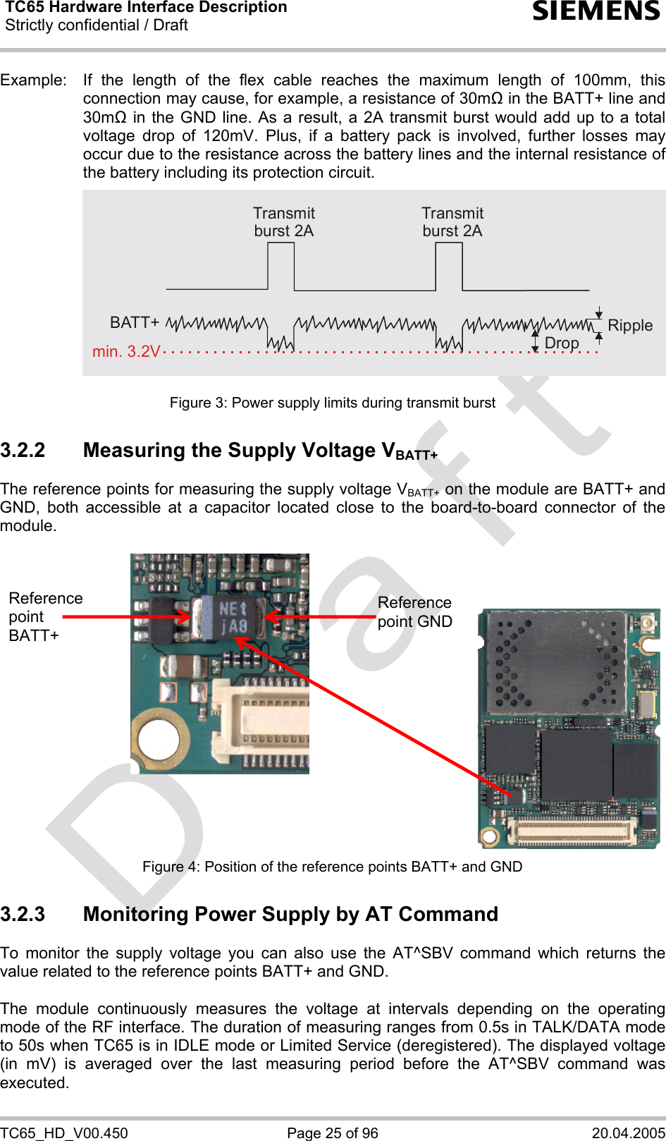
![TC65 Hardware Interface Description Strictly confidential / Draft s TC65_HD_V00.450 Page 8 of 96 20.04.2005 1 Introduction This document describes the hardware of the Siemens TC65 module that connects to the cellular device application and the air interface. It helps you quickly retrieve interface specifications, electrical and mechanical details and information on the requirements to be considered for integrating further components. 1.1 Related Documents [1] TC65 AT Command Set [2] TC65 Release Notes 00.450 [3] DSB75 Support Box - Evaluation Kit for Siemens Cellular Engines [4] Application 07: Rechargeable Lithium Batteries in GSM Applications (not yet available) [5] Multiplexer User's Guide (not yet available)](https://usermanual.wiki/THALES-DIS-AlS-Deutschland/TC65.Users-Manual-1-of-2/User-Guide-550087-Page-8.png)
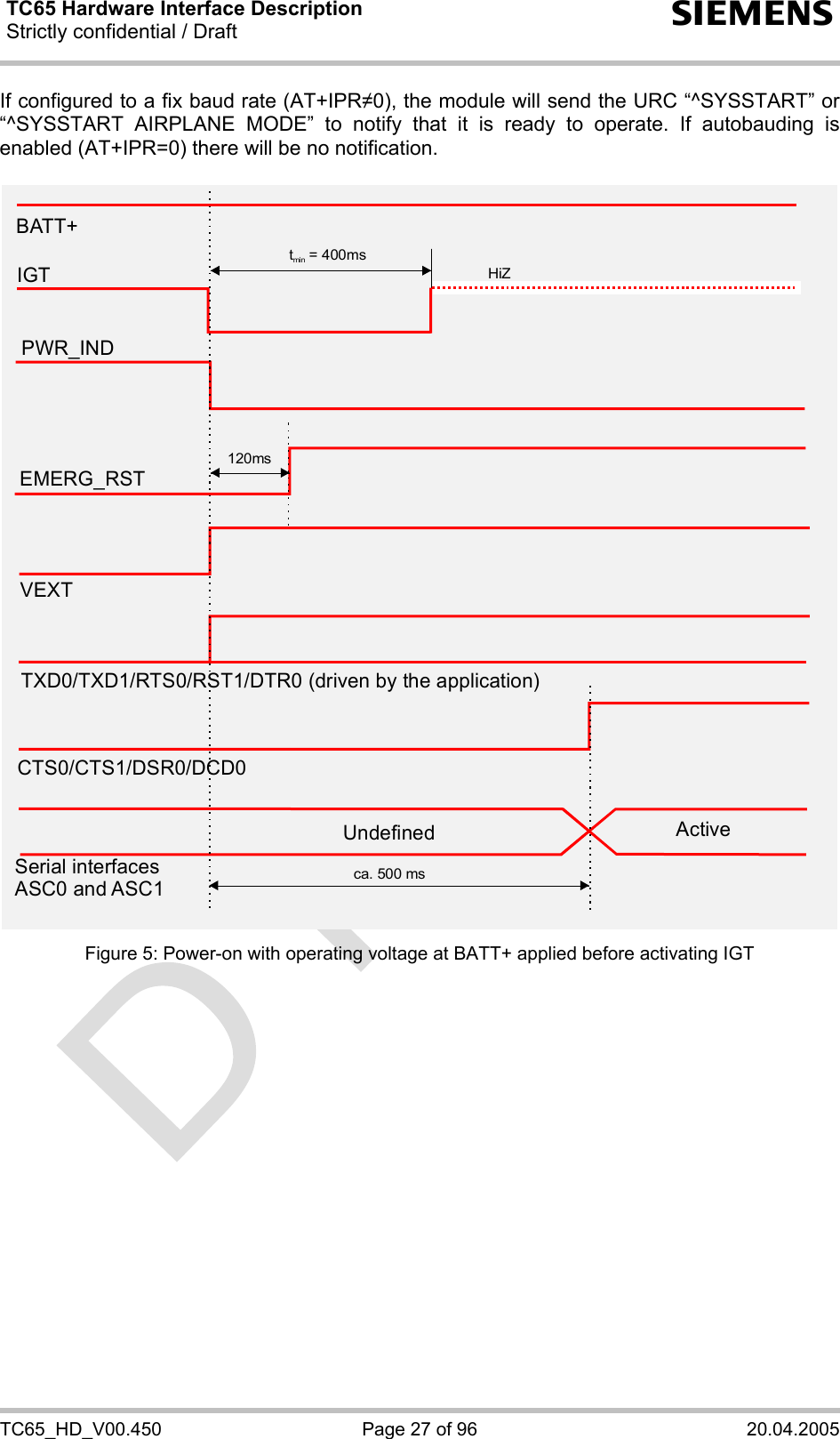
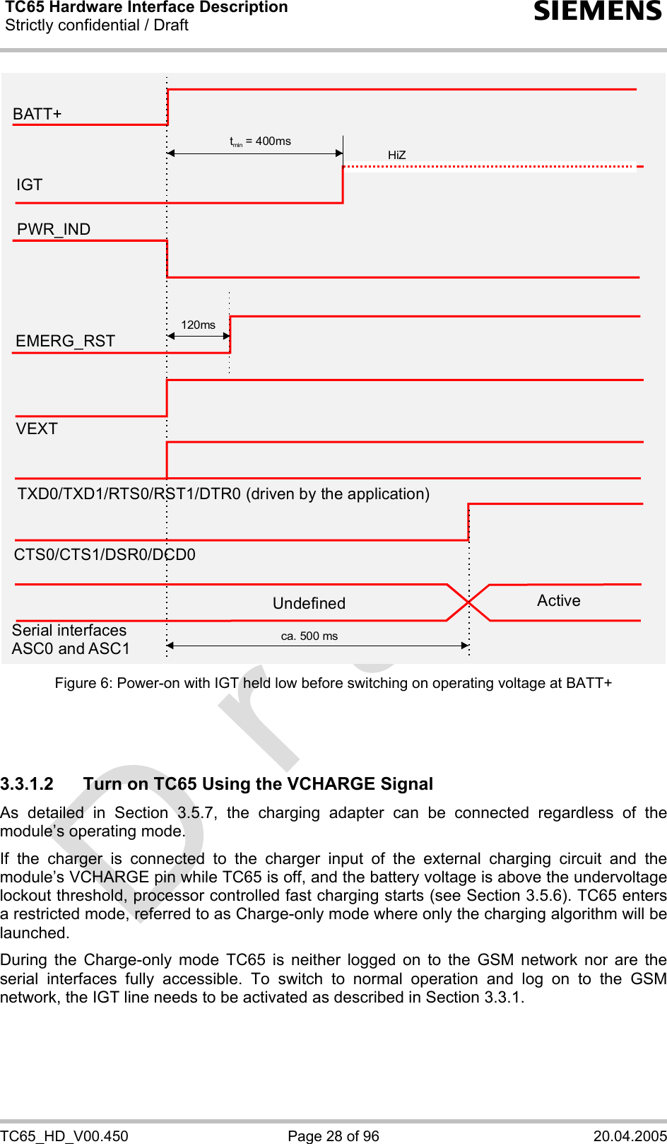
![TC65 Hardware Interface Description Strictly confidential / Draft s TC65_HD_V00.450 Page 26 of 96 20.04.2005 3.3 Power Up / Power Down Scenarios In general, be sure not to turn on TC65 while it is beyond the safety limits of voltage and temperature stated in Chapter 5. TC65 would immediately switch off after having started and detected these inappropriate conditions. In extreme cases this can cause permanent damage to the module. 3.3.1 Turn on TC65 TC65 can be started in a variety of ways as described in the following sections: • Hardware driven start-up by IGT line: starts Normal mode or Airplane mode (see Section 3.3.1.1) • Software controlled reset by AT+CFUN command: starts Normal mode or Airplane mode (see Section 3.3.1.3) • Hardware driven start-up by VCHARGE line: starts charging algorithm and charge-only mode (see Section 3.3.1.2) • Wake-up from Power-down mode by using RTC interrupt: starts Airplane mode The option whether to start into Normal mode or Airplane mode depends on the settings made with the AT^SCFG command or AT+CALA. With AT+CALA, followed by AT^SMSO the module can be configured to restart into Airplane mode at a scheduled alarm time. Switching back and forth between Normal mode and Airplane mode is possible any time during operation by using the AT^SCFG command. After startup or mode change the following URCs indicate the module’s ready state: • “SYSSTART” indicates that the module has entered Normal mode. • “^SYSSTART AIRPLANE MODE” indicates that the module has entered Airplane mode. • “^SYSSTART CHARGE ONLY MODE” indicates that the module has entered the Charge-only mode. Detailed explanations on AT^SCFG, AT+CFUN, AT+CALA and Airplane mode can be found in [1]. 3.3.1.1 Turn on TC65 Using Ignition Line IGT When the TC65 module is in Power-down mode, it can be started to Normal mode or Airplane mode by driving the IGT (ignition) line to ground. This must be accomplished with an open drain/collector driver to avoid current flowing into this pin. The module will start up when both of the following two conditions are met: • The supply voltage applied at BATT+ must be in the operating range. • The IGT line needs to be driven low for at least 400ms. Considering different strategies of host application design the figures below show two approaches to meet this requirement: The example in Figure 5 assumes that IGT is activated after BATT+ has already been applied. The example in Figure 6 assumes that IGT is held low before BATT+ is switched on. In either case, to power on the module, ensure that low state of IGT takes at least 400ms from the moment the voltage at BATT+ is available.](https://usermanual.wiki/THALES-DIS-AlS-Deutschland/TC65.Users-Manual-1-of-2/User-Guide-550087-Page-26.png)
![TC65 Hardware Interface Description Strictly confidential / Draft s TC65_HD_V00.450 Page 29 of 96 20.04.2005 3.3.1.3 Reset TC65 via AT+CFUN Command To reset and restart the TC65 module use the command AT+CFUN. You can enter AT+CFUN=,1 or AT+CFUN=x,1, where x may be in the range from 0 to 9. See [1] for details. If configured to a fix baud rate (AT+IPR0), the module will send the URC “^SYSSTART” or “^SYSSTART AIRPLANE MODE” to notify that it is ready to operate. If autobauding is enabled (AT+IPR=0) there will be no notification. To register to the network SIM PIN authentication is necessary after restart. 3.3.1.4 Reset TC65 in Case of Emergency via EMERG_RST Caution: Use the EMERG_RST pin only when, due to serious problems, the software is not responding for more than 5 seconds. Pulling the EMERG_RST pin causes the loss of all information stored in the volatile memory since the processor restarts immediately. Therefore, this procedure is intended only for use in case of emergency, e.g. if TC65 does not respond, if reset or shutdown via AT command fails. The EMERG_RST signal is available on the application interface. To control the EMERG_RST line it is recommended to use an open drain / collector driver. To actually reset the TC65 module, the EMERG_RST line must be pulled to ground for ≥10ms. After releasing the line TC65 will start again. After hardware driven restart, notification via “^SYSSTART” or “^SYSSTART AIRPLANE” URC is the same as in case of restart by IGT or AT command. To register to the network SIM PIN authentication is necessary after restart.](https://usermanual.wiki/THALES-DIS-AlS-Deutschland/TC65.Users-Manual-1-of-2/User-Guide-550087-Page-29.png)
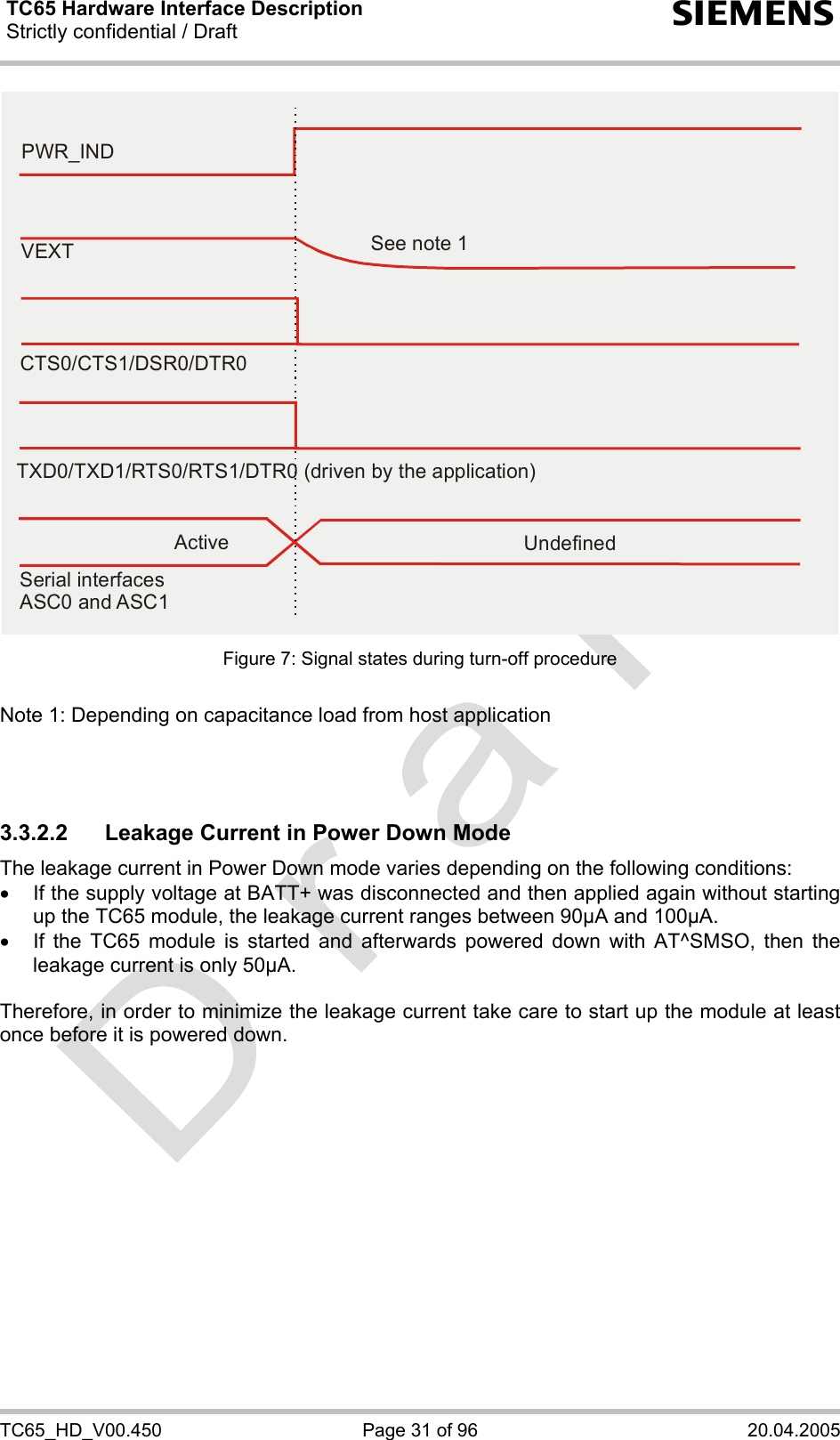
![TC65 Hardware Interface Description Strictly confidential / Draft s TC65_HD_V00.450 Page 32 of 96 20.04.2005 3.3.3 Automatic Shutdown Automatic shutdown takes effect if: • the TC65 board is exceeding the critical limits of overtemperature or undertemperature • the battery is exceeding the critical limits of overtemperature or undertemperature • undervoltage or overvoltage is detected See Charge-only mode described in section 3.5.7 for exceptions. The automatic shutdown procedure is equivalent to the Power-down initiated with the AT^SMSO command, i.e. TC65 logs off from the network and the software enters a secure state avoiding loss of data. Alert messages transmitted before the device switches off are implemented as Unsolicited Result Codes (URCs). The presentation of these URCs can be enabled or disabled with the two AT commands AT^SBC and AT^SCTM. The URC presentation mode varies with the condition, please see Chapters 3.3.3.1 to 3.3.3.4 for details. For further instructions on AT commands refer to [1]. 3.3.3.1 Temperature Dependent Shutdown The board temperature is constantly monitored by an internal NTC resistor located on the PCB. The NTC that detects the battery temperature must be part of the battery pack circuit as described in 3.5.3 The values detected by either NTC resistor are measured directly on the board or the battery and therefore, are not fully identical with the ambient temperature. Each time the board or battery temperature goes out of range or back to normal, TC65 instantly displays an alert (if enabled). • URCs indicating the level "1" or "-1" allow the user to take appropriate precautions, such as protecting the module from exposure to extreme conditions. The presentation of the URCs depends on the settings selected with the AT^SCTM write command: AT^SCTM=1: Presentation of URCs is always enabled. AT^SCTM=0 (default): Presentation of URCs is enabled for 15 seconds time after start-up of TC65. After 15 seconds operation, the presentation will be disabled, i.e. no alert messages can be generated. • URCs indicating the level "2" or "-2" are instantly followed by an orderly shutdown. The presentation of these URCs is always enabled, i.e. they will be output even though the factory setting AT^SCTM=0 was never changed. The maximum temperature ratings are stated in Table 16. Refer to Table 2 for the associated URCs. All statements are based on test conditions according to IEC 60068-2-2 (still air).](https://usermanual.wiki/THALES-DIS-AlS-Deutschland/TC65.Users-Manual-1-of-2/User-Guide-550087-Page-32.png)
![TC65 Hardware Interface Description Strictly confidential / Draft s TC65_HD_V00.450 Page 33 of 96 20.04.2005 Table 2: Temperature dependent behavior Sending temperature alert (15s after TC65 start-up, otherwise only if URC presentation enabled) ^SCTM_A: 1 Caution: Tamb of battery close to overtemperature limit. ^SCTM_B: 1 Caution: Tamb of board close to overtemperature limit. ^SCTM_A: -1 Caution: Tamb of battery close to undertemperature limit. ^SCTM_B: -1 Caution: Tamb of board close to undertemperature limit. ^SCTM_A: 0 Battery back to uncritical temperature range. ^SCTM_B: 0 Board back to uncritical temperature range. Automatic shutdown (URC appears no matter whether or not presentation was enabled) ^SCTM_A: 2 Alert: Tamb of battery equal or beyond overtemperature limit. TC65 switches off.^SCTM_B: 2 Alert: Tamb of board equal or beyond overtemperature limit. TC65 switches off. ^SCTM_A: -2 Alert: Tamb of battery equal or below undertemperature limit. TC65 switches off. ^SCTM_B: -2 Alert: Tamb of board equal or below undertemperature limit. TC65 switches off. 3.3.3.2 Temperature Control during Emergency call If the temperature limit is exceeded while an emergency call is in progress the engine continues to measure the temperature, but deactivates the shutdown functionality. If the temperature is still out of range when the call ends, the module switches off immediately (without another alert message). 3.3.3.3 Undervoltage Shutdown if Battery NTC is Present In applications where the module’s charging technique is used and an NTC is connected to the BATT_TEMP terminal, the software constantly monitors the applied voltage. If the measured battery voltage is no more sufficient to set up a call the following URC will be presented: ^SBC: Undervoltage. The message will be reported, for example, when you attempt to make a call while the voltage is close to the shutdown threshold of 3.2V and further power loss is caused during the transmit burst. In IDLE mode, the shutdown threshold is the sum of the module’s minimum supply voltage (3.2V) and the value of the maximum voltage drop resulting from earlier calls. This means that in IDLE mode the actual shutdown threshold may be higher than 3.2V. Therefore, to properly calculate the actual shutdown threshold application manufacturers are advised to measure the maximum voltage drops that may occur during transmit bursts. To remind you that the battery needs to be charged soon, the URC appears several times before the module switches off. To enable or disable the URC use the AT^SBC command. The URC will be enabled when you enter the write command and specify the current consumption of your host application. Step by step instructions are provided in [1].](https://usermanual.wiki/THALES-DIS-AlS-Deutschland/TC65.Users-Manual-1-of-2/User-Guide-550087-Page-33.png)
![TC65 Hardware Interface Description Strictly confidential / Draft s TC65_HD_V00.450 Page 36 of 96 20.04.2005 3.5 Charging Control TC65 integrates a charging management for rechargeable Lithium Ion and Lithium Polymer batteries. You can skip this chapter if charging is not your concern, or if you are not using the implemented charging algorithm. The following sections contain an overview of charging and battery specifications. Please refer to [4] for greater detail, especially regarding requirements for batteries and chargers, appropriate charging circuits, recommended batteries and an analysis of operational issues typical of battery powered GSM/GPRS applications. 3.5.1 Hardware Requirements TC65 has no on-board charging circuit. To benefit from the implemented charging management you are required to install a charging circuit within your application according to the Figure 38. 3.5.2 Software Requirements Use the command AT^SBC, parameter <current>, to enter the current consumption of the host application. This information enables the TC65 module to correctly determine the end of charging and terminate charging automatically when the battery is fully charged. If the <current> value is inaccurate and the application draws a current higher than the final charge current, either charging will not be terminated or the battery fails to reach its maximum voltage. Therefore, the termination condition is defined as: final charge current (50mA) plus current consumption of the external application. If used the current flowing over the VEXT pin of the application interface (typically 2.9V) must be added, too. The parameter <current> is volatile, meaning that the factory default (0mA) is restored each time the module is powered down or reset. Therefore, for better control of charging, it is recommended to enter the value every time the module is started. See [1] for details on AT^SBC.](https://usermanual.wiki/THALES-DIS-AlS-Deutschland/TC65.Users-Manual-1-of-2/User-Guide-550087-Page-36.png)
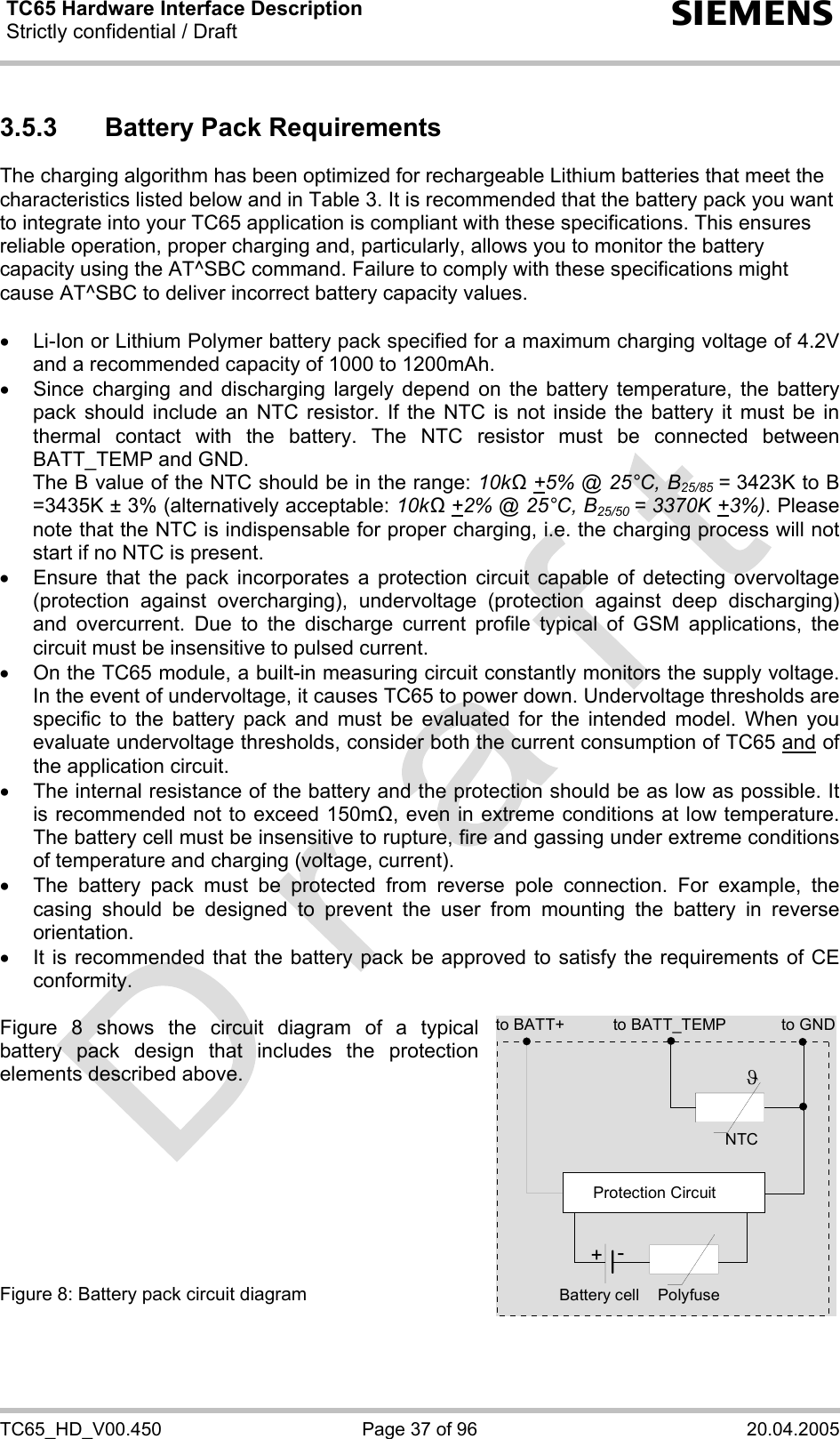
![TC65 Hardware Interface Description Strictly confidential / Draft s TC65_HD_V00.450 Page 39 of 96 20.04.2005 3.5.5 Charger Requirements For using the implemented charging algorithm and the reference charging circuit recommended in [4] and in Figure 38, the charger has to meet the following requirements: Output voltage: 5.2Volts ±0.2V (stabilized voltage) Output current: 500mA Chargers with a higher output current are acceptable, but please consider that only 500mA will be applied when a 0.3Ohms shunt resistor is connected between VSENSE and ISENSE. See [4] for further details. 3.5.6 Implemented Charging Technique If all requirements listed above are met (appropriate external charging circuit of application, battery pack, charger, AT^SBC settings) then charging is enabled in various stages depending on the battery condition: Trickle charging: • Trickle charge current flows over the VCHARGE line. • Trickle charging is done when a charger is present (connected to VCHARGE) and the battery is deeply discharged or has undervoltage. If deeply discharged (Deep Discharge Lockout at VBATT+= 0…2.5V) the battery is charged with 5mA, in case of undervoltage (Undervoltage Lockout at VBATT+= 2.5…3.2V) it is charged with 30mA Software controlled charging: • Controlled over the CHARGEGATE. • Temperature conditions: 0°C to 45°C • Software controlled charging is done when the charger is present (connected to VCHARGE) and the battery voltage is at least above the undervoltage threshold. Software controlled charging passes the following stages: - Power ramp: Depending on the discharge level of the battery (i.e. the measured battery voltage VBATT+) the software adjusts the maximum charge current for charging the battery. The duration of power ramp charging is very short (less than 30 seconds). - Fast charging: Battery is charged with constant current (approx. 500mA) until the battery voltage reaches 4.2V (approx. 80% of the battery capacity). - Top-up charging: The battery is charged with constant voltage of 4.2V at stepwise reducing charge current until full battery capacity is reached. • The duration of software controlled charging depends on the battery capacity and the level of discharge.](https://usermanual.wiki/THALES-DIS-AlS-Deutschland/TC65.Users-Manual-1-of-2/User-Guide-550087-Page-39.png)
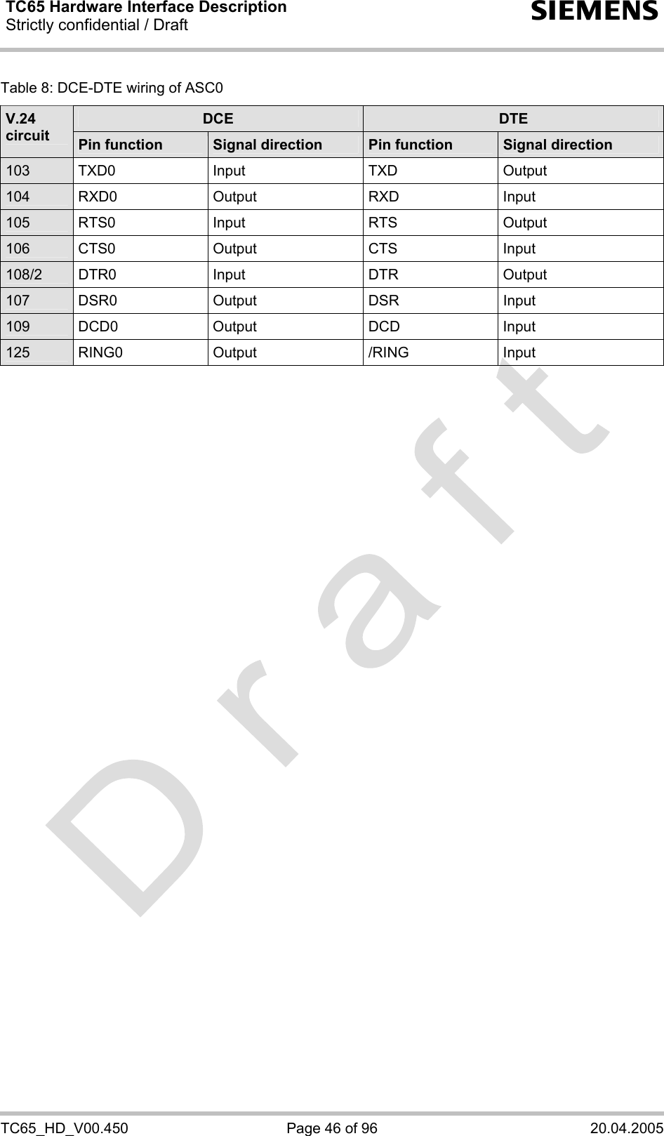
![TC65 Hardware Interface Description Strictly confidential / Draft s TC65_HD_V00.450 Page 45 of 96 20.04.2005 3.9 Serial Interface ASC0 TC65 offers an 8-wire unbalanced, asynchronous modem interface ASC0 conforming to ITU-T V.24 protocol DCE signalling. The electrical characteristics do not comply with ITU-T V.28. The significant levels are 0V (for low data bit or active state) and 2.9V (for high data bit or inactive state). For electrical characteristics please refer to Table 17. TC65 is designed for use as a DCE. Based on the conventions for DCE-DTE connections it communicates with the customer application (DTE) using the following signals: • Port TXD @ application sends data to the module’s TXD0 signal line • Port RXD @ application receives data from the module’s RXD0 signal line GSM module (DCE) Application (DTE)TXDRXDRTSCTSRINGDCDDSRDTRTXD0RXD0RTS0CTS0RING0DCD0DSR0DTR0 Figure 12: Serial interface ASC0 Features • Includes the data lines TXD0 and RXD0, the status lines RTS0 and CTS0 and, in addition, the modem control lines DTR0, DSR0, DCD0 and RING0. • ASC0 is primarily designed for controlling voice calls, transferring CSD, fax and GPRS data and for controlling the GSM engine with AT commands. • Full Multiplex capability allows the interface to be partitioned into three virtual channels, yet with CSD and fax services only available on the first logical channel. Please note that when the ASC0 interface runs in Multiplex mode, ASC1 cannot be used. For more details on Multiplex mode see [5]. • The DTR0 signal will only be polled once per second from the internal firmware of TC65. • The RING0 signal serves to indicate incoming calls and other types of URCs (Unsolicited Result Code). It can also be used to send pulses to the host application, for example to wake up the application from power saving state. See [1] for details on how to configure the RING0 line by AT^SCFG. • By default, configured for 8 data bits, no parity and 1 stop bit. The setting can be changed using the AT command AT+ICF and, if required, AT^STPB. For details see [1]. • ASC0 can be operated at bit rates from 300bps to 460800bps. • Autobauding supports the following bit rates: TBD. • Autobauding is not compatible with multiplex mode. • Supports RTS0/CTS0 hardware flow control and XON/XOFF software flow control.](https://usermanual.wiki/THALES-DIS-AlS-Deutschland/TC65.Users-Manual-1-of-2/User-Guide-550087-Page-45.png)
![TC65 Hardware Interface Description Strictly confidential / Draft s TC65_HD_V00.450 Page 47 of 96 20.04.2005 3.10 Serial Interface ASC1 TC65 offers a 4-wire unbalanced, asynchronous modem interface ASC1 conforming to ITU-T V.24 protocol DCE signalling. The electrical characteristics do not comply with ITU-T V.28. The significant levels are 0V (for low data bit or active state) and 2.9V (for high data bit or inactive state). For electrical characteristics please refer to Table 17. TC65 is designed for use as a DCE. Based on the conventions for DCE-DTE connections it communicates with the customer application (DTE) using the following signals: • Port TXD @ application sends data to module’s TXD1 signal line • Port RXD @ application receives data from the module’s RXD1 signal line GSM module (DCE) Application (DTE)TXDRXDRTSCTSTXD1RXD1RTS1CTS1 Figure 13: Serial interface ASC1 Features • Includes only the data lines TXD1 and RXD1 plus RTS1 and CTS1 for hardware handshake. • On ASC1 no RING line is available. The indication of URCs on the second interface depends on the settings made with the AT^SCFG command. For details refer to [1]. • Configured for 8 data bits, no parity and 1 or 2 stop bits. • ASC1 can be operated at bit rates from 300bps to 460800bps. • Autobauding TBD. • Supports RTS1/CTS1 hardware flow control and XON/XOFF software flow control. Table 9: DCE-DTE wiring of ASC1 DCE DTE V.24 circuit Pin function Signal direction Pin function Signal direction 103 TXD1 Input TXD Output 104 RXD1 Output RXD Input 105 RTS1 Input RTS Output 106 CTS1 Output CTS Input](https://usermanual.wiki/THALES-DIS-AlS-Deutschland/TC65.Users-Manual-1-of-2/User-Guide-550087-Page-47.png)