THALES DIS AlS Deutschland TC65 Quadband GSM/GPRS Module User Manual TC65
Gemalto M2M GmbH Quadband GSM/GPRS Module TC65
UserManual.wiki
>
THALES DIS AlS Deutschland
>
TC65 User Manual
>
Users Manual 2 of 2
Contents
1.
Users Manual 1 of 2
2.
Users Manual 2 of 2
Users Manual 2 of 2
Navigation menu
Upload a User Manual
Namespaces
Wiki Guide
HTML
PDF
Info
Views
User Manual
Discussion / Help
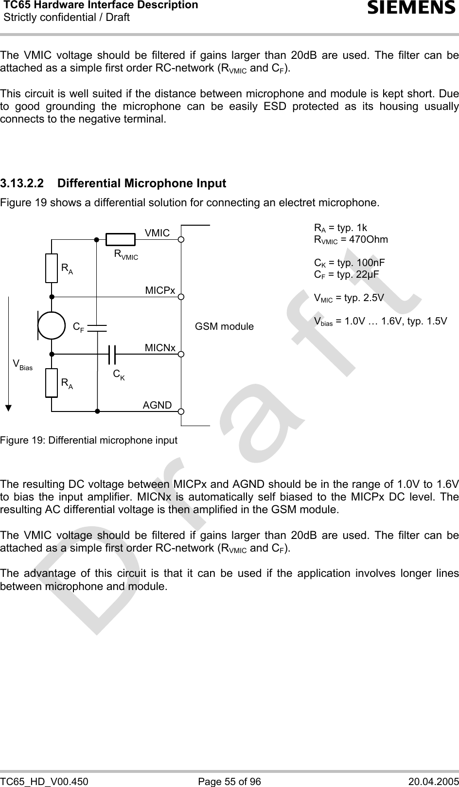
Navigation
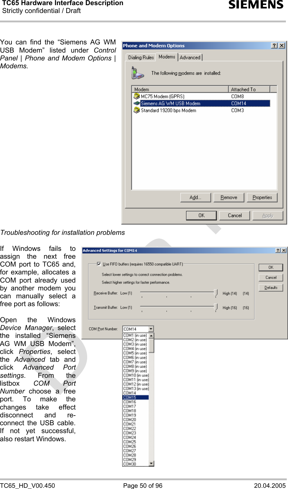
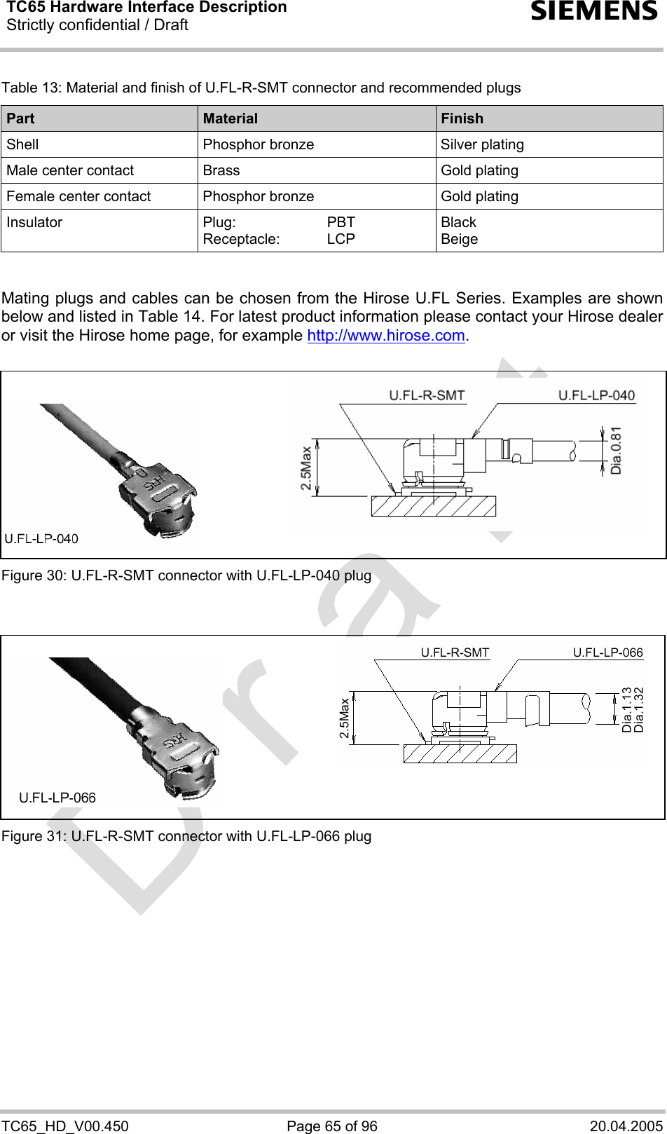
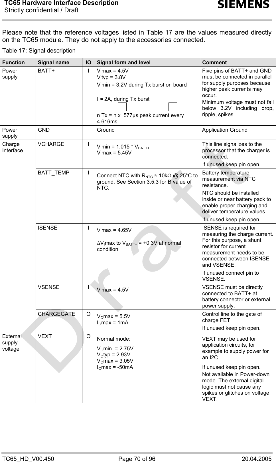
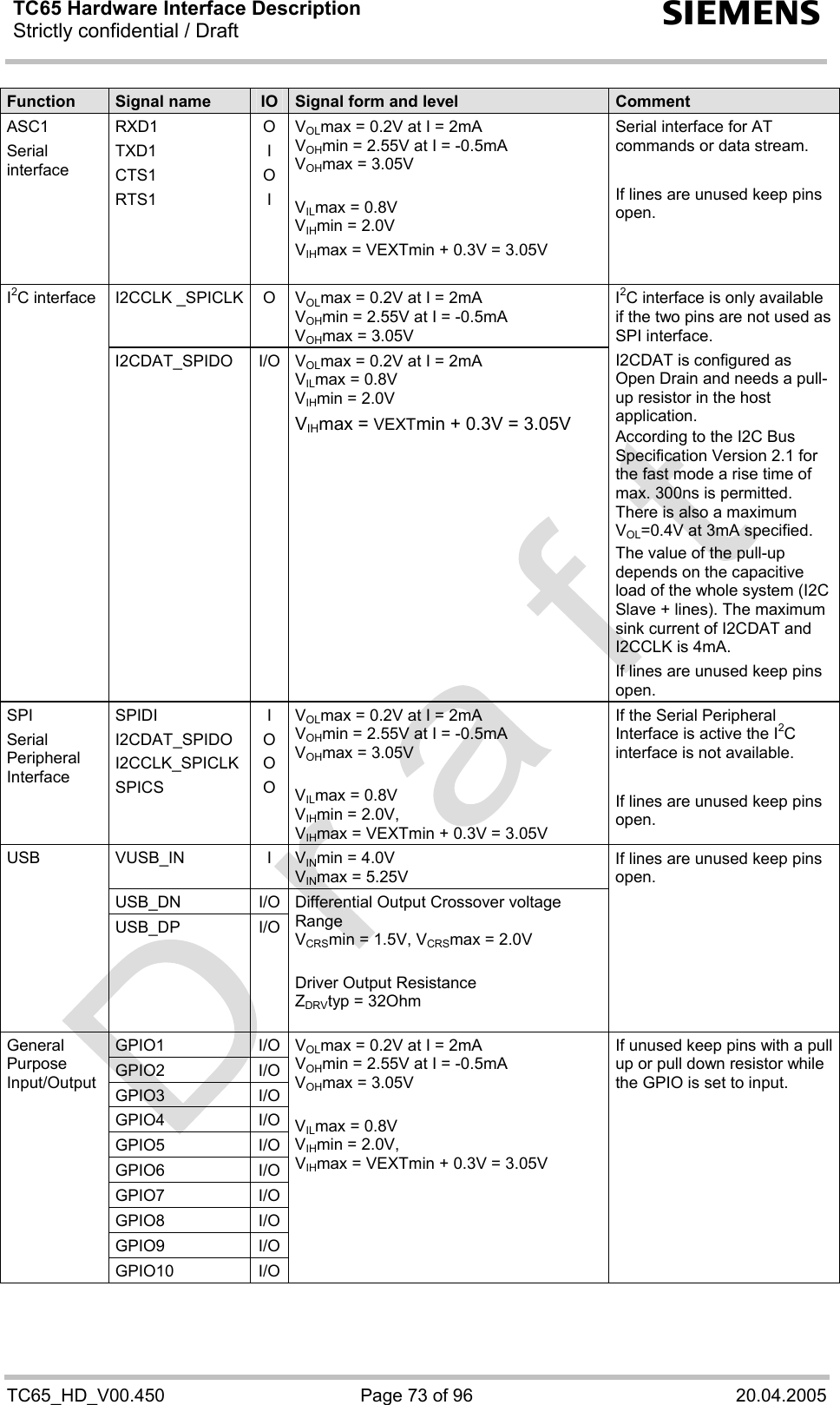
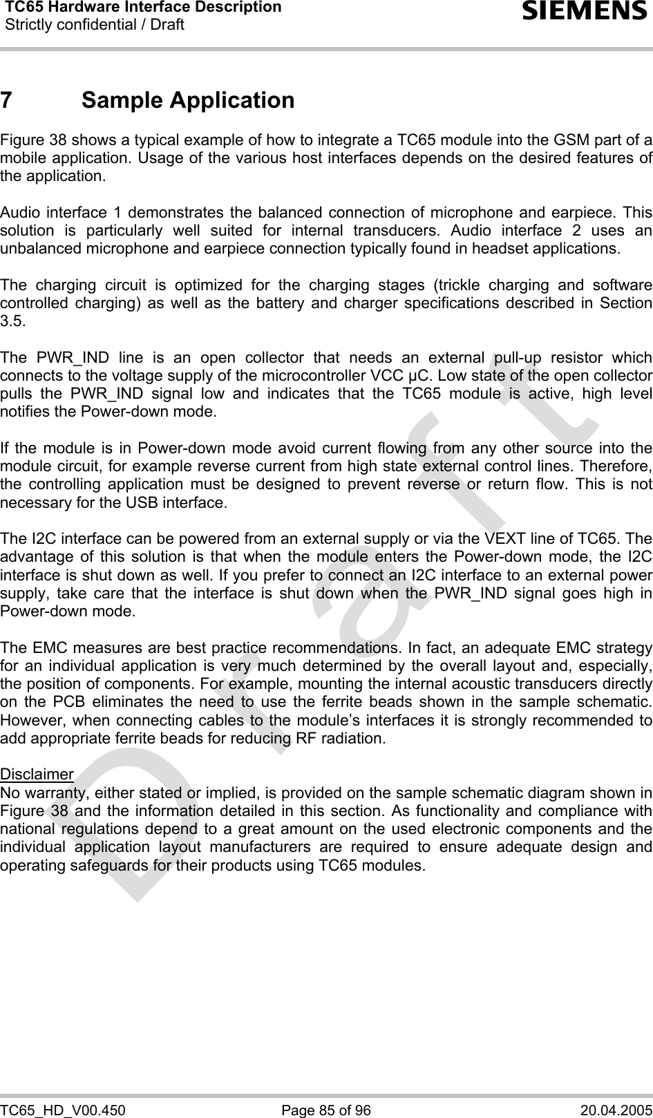
![TC65 Hardware Interface Description Strictly confidential / Draft s TC65_HD_V00.450 Page 51 of 96 20.04.2005 3.12 I2C Interface I2C is a serial, 8-bit oriented data transfer bus for bit rates up to 400kbps in Fast mode. It consists of two lines, the serial data line I2CDAT and the serial clock line I2CCLK. The TC65 module acts as a single master device, e.g. the clock I2CCLK is driven by module. I2CDAT is a bi-directional line. Each device connected to the bus is software addressable by a unique 7-bit address, and simple master/slave relationships exist at all times. The module operates as master-transmitter or as master-receiver. The customer application transmits or receives data only on request of the module. To configure and activate the I2C bus use the AT^SSPI command. If the I2C bus is active the two lines I2CCLK and I2DAT are locked for use as SPI lines. Vice versa, the activation of the SPI locks both lines for I2C. Detailed information on the AT^SSPI command as well explanations on the protocol and syntax required for data transmission can be found in [1]. The I2C interface can be powered from an external supply or via the VEXT line of TC65. If connected to the VEXT line the I2C interface will be properly shut down when the module enters the Power-down mode. If you prefer to connect the I2C interface to an external power supply, take care that VCC of the application is in the range of VVEXT and that the interface is shut down when the PWR_IND signal goes high. See figures below as well as Section 7 and Figure 38. In the application I2CDAT and I2CCLK lines need to be connected to a positive supply voltage via a pull-up resistor. For electrical characteristics please refer to Table 17. GSM moduleI2CDATI2CCLKGNDI2CDATI2CCLKGNDApplicationVCCRpRpwVEXT Figure 15: I2C interface connected to VCC of application](https://usermanual.wiki/THALES-DIS-AlS-Deutschland/TC65.Users-Manual-2-of-2/User-Guide-550088-Page-3.png)
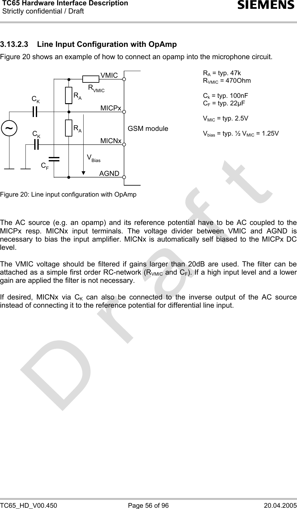
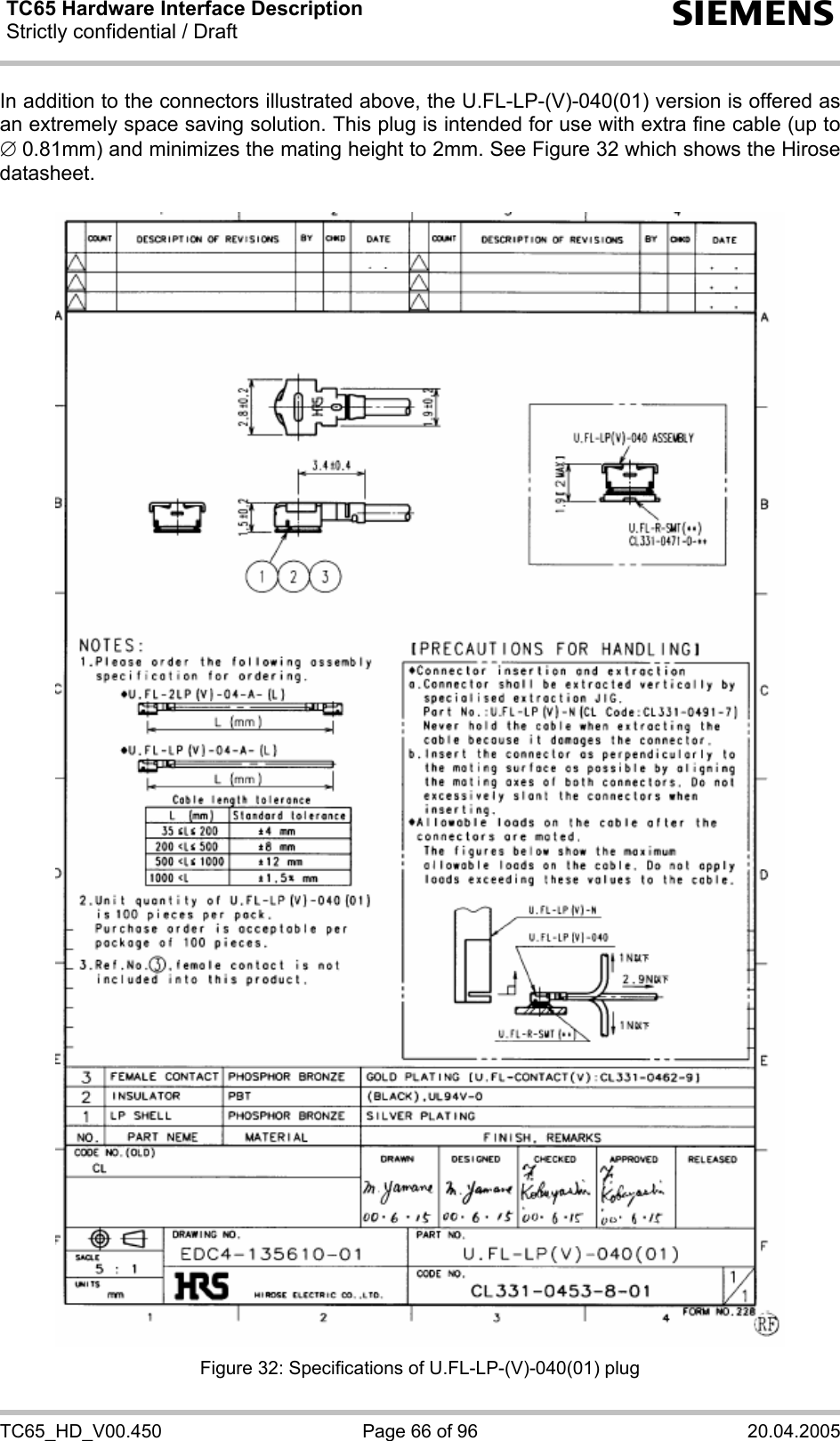
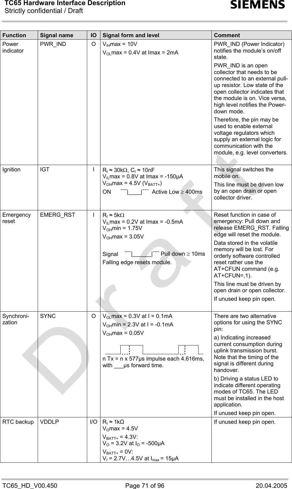
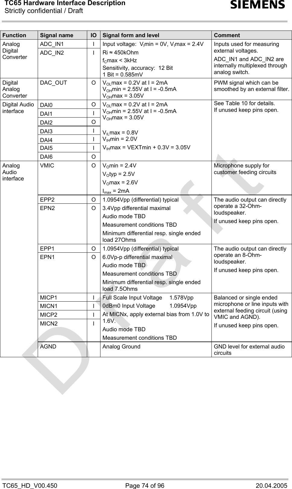
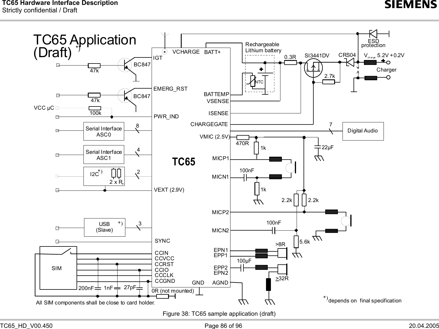
![TC65 Hardware Interface Description Strictly confidential / Draft s TC65_HD_V00.450 Page 59 of 96 20.04.2005 3.14 Control Signals 3.14.1 Synchronization Signal The synchronization signal serves to indicate growing power consumption during the transmit burst. The signal is generated by the SYNC pin (pin number 32). Please note that this pin can adopt three different operating modes which you can select by using the AT^SSYNC command: the mode AT^SSYNC=0 described below, and the two LED modes AT^SSYNC=1 or AT^SSYNC=2 described in [1] and Section 3.14.2. The first function (factory default AT^SSYNC=0) is recommended if you want your application to use the synchronization signal for better power supply control. Your platform design must be such that the incoming signal accommodates sufficient power supply to the TC65 module if required. This can be achieved by lowering the current drawn from other components installed in your application. The timing of the synchronization signal is shown below. High level of the SYNC pin indicates increased power consumption during transmission. Figure 25: SYNC signal during transmit burst *) The duration of the SYNC signal is always equal, no matter whether the traffic or the access burst are active. Transmit burst1 Tx 577 µs every 4.616 ms2 Tx 1154 µs every 4.616 msSYNC signal*)t = 180 sµ](https://usermanual.wiki/THALES-DIS-AlS-Deutschland/TC65.Users-Manual-2-of-2/User-Guide-550088-Page-11.png)
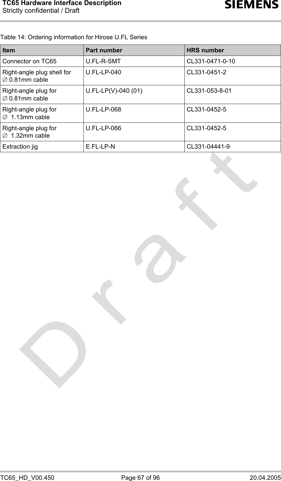
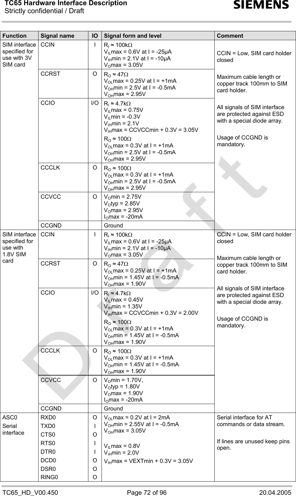
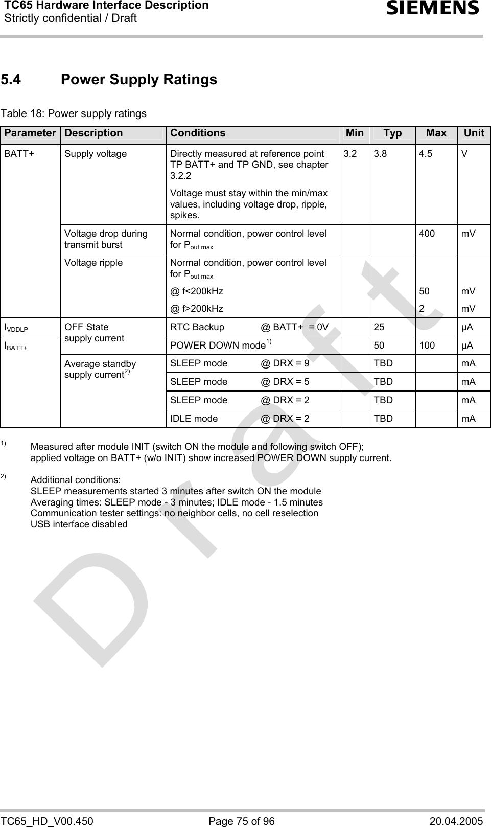
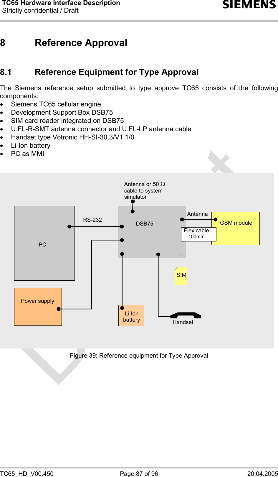
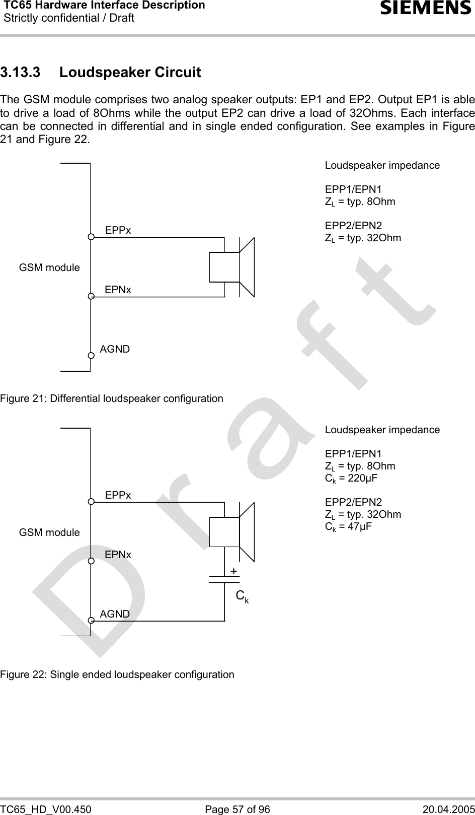
![TC65 Hardware Interface Description Strictly confidential / Draft s TC65_HD_V00.450 Page 60 of 96 20.04.2005 3.14.2 Using the SYNC Pin to Control a Status LED As an alternative to generating the synchronization signal, the SYNC pin can be configured to drive a status LED that indicates different operating modes of the TC65 module. To take advantage of this function the LED mode must be activated with the AT^SSYNC command and the LED must be connected to the host application. The connected LED can be operated in two different display modes (AT^SSYNC=1 or AT^SSYNC=2). For details please refer to [1]. Especially in the development and test phase of an application, system integrators are advised to use the LED mode of the SYNC pin in order to evaluate their product design and identify the source of errors. To operate the LED a buffer, e.g. a transistor or gate, must be included in your application. A sample circuit is shown in Figure 26. Power consumption in the LED mode is the same as for the synchronization signal mode. For details see Table 17, SYNC pin. Figure 26: LED Circuit (Example)](https://usermanual.wiki/THALES-DIS-AlS-Deutschland/TC65.Users-Manual-2-of-2/User-Guide-550088-Page-12.png)