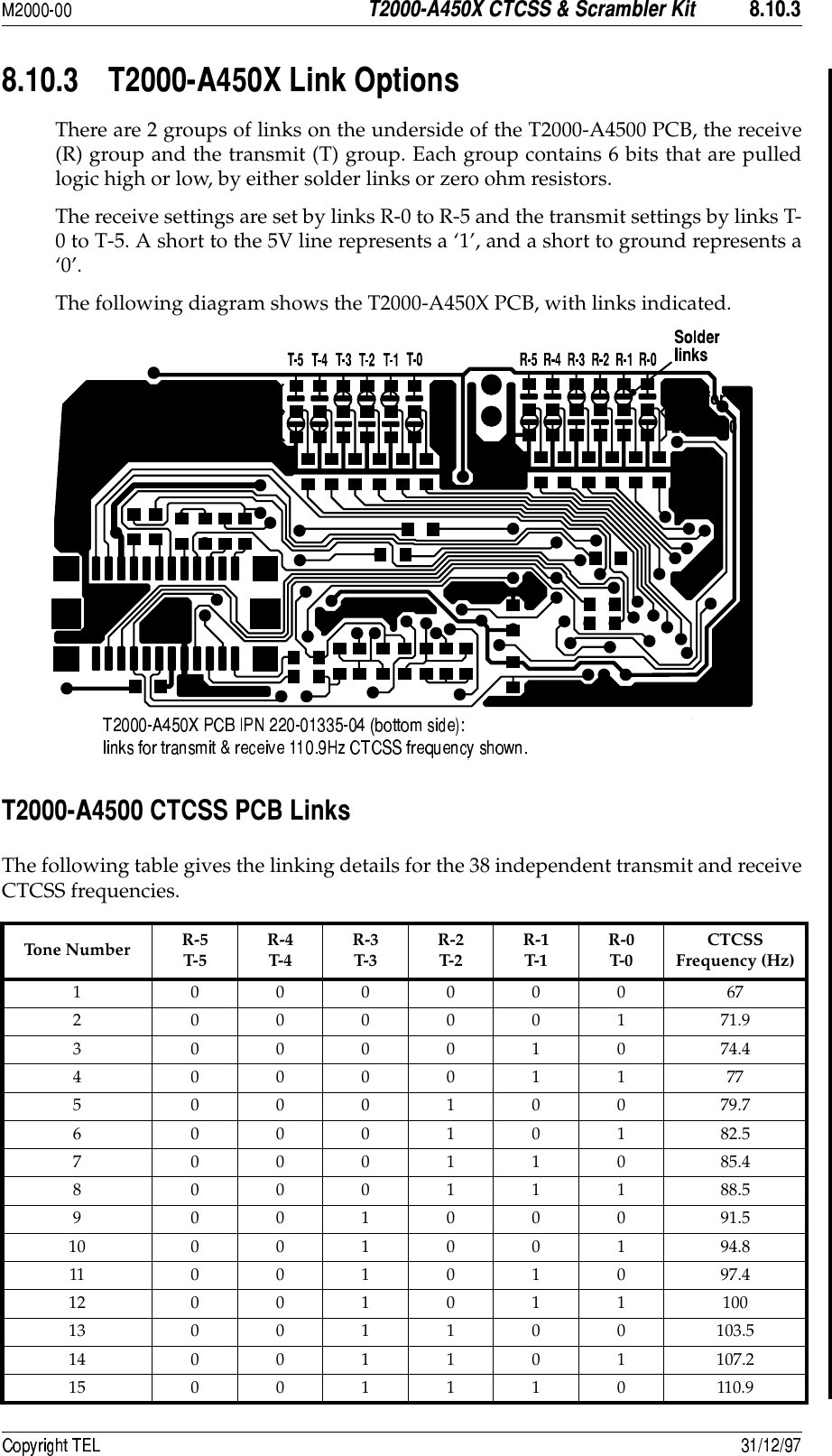
Tait T2010-313 Mobile Transceiver User Manual 2k3 03
Tait Limited Mobile Transceiver 2k3 03
UserManual.wiki
>
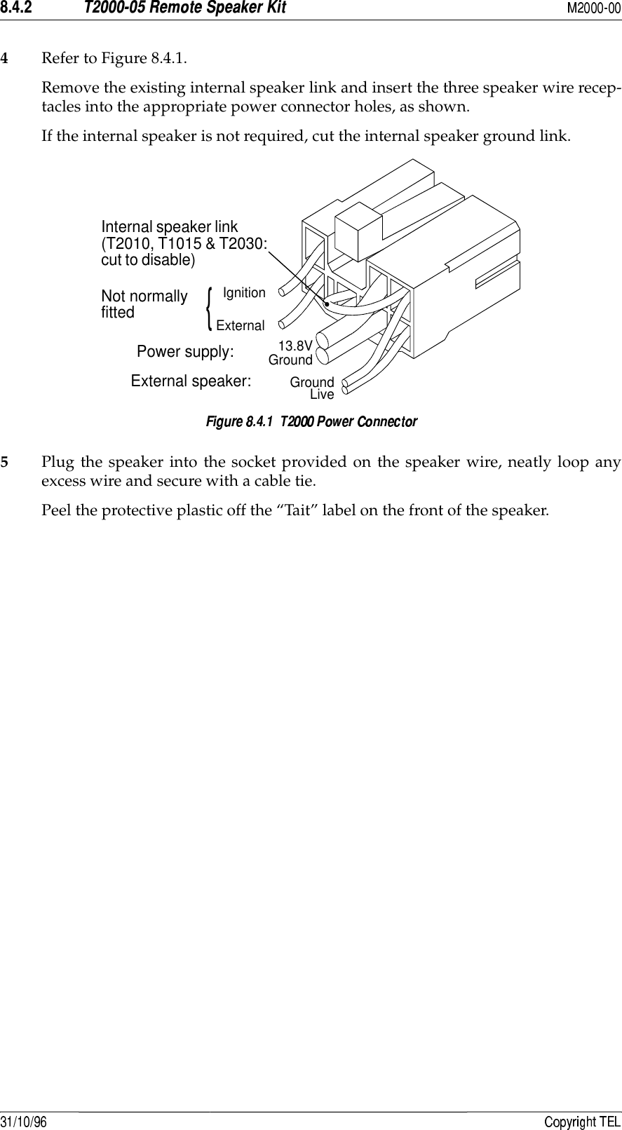
Tait
>
T2010-313 User Manual
>
user manual part 5
Contents
1.
reference to T2000 user manual
2.
user manual part 1
3.
user manual part 2
4.
user manual part 3
5.
user manual part 4
6.
user manual part 5
7.
user manual part 6
8.
user manual part 7
9.
user manual part 8
10.
user manual part 9
11.
user manual part 10
user manual part 5
Navigation menu
Upload a User Manual
Namespaces
Wiki Guide
HTML
PDF
Info
Views
User Manual
Discussion / Help
Navigation