Tait T2010-313 Mobile Transceiver User Manual 2k3 03
Tait Limited Mobile Transceiver 2k3 03
UserManual.wiki
>
Tait
>
T2010-313 User Manual
>
user manual part 6
Contents
1.
reference to T2000 user manual
2.
user manual part 1
3.
user manual part 2
4.
user manual part 3
5.
user manual part 4
6.
user manual part 5
7.
user manual part 6
8.
user manual part 7
9.
user manual part 8
10.
user manual part 9
11.
user manual part 10
user manual part 6
Navigation menu
Upload a User Manual
Namespaces
Wiki Guide
HTML
PDF
Info
Views
User Manual
Discussion / Help
Navigation
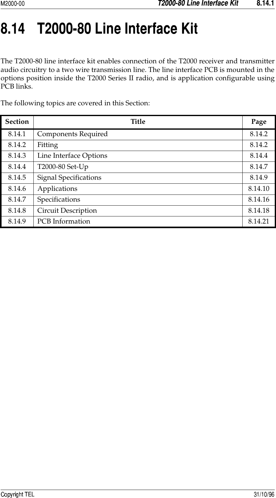
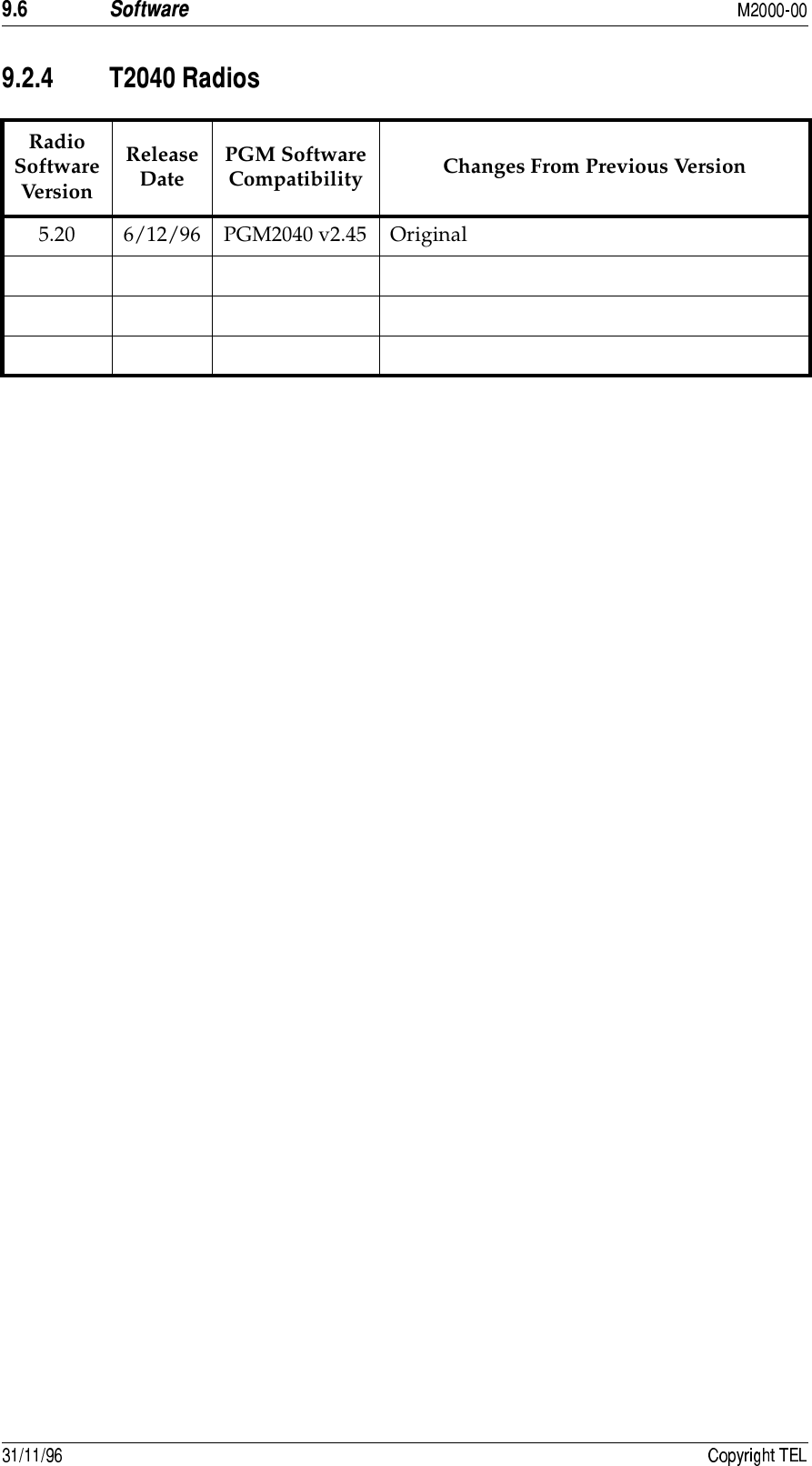
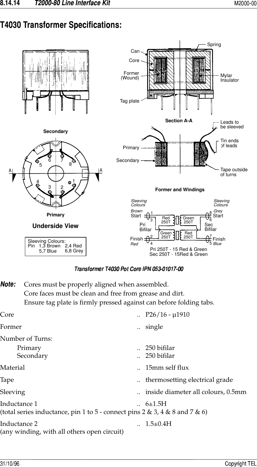
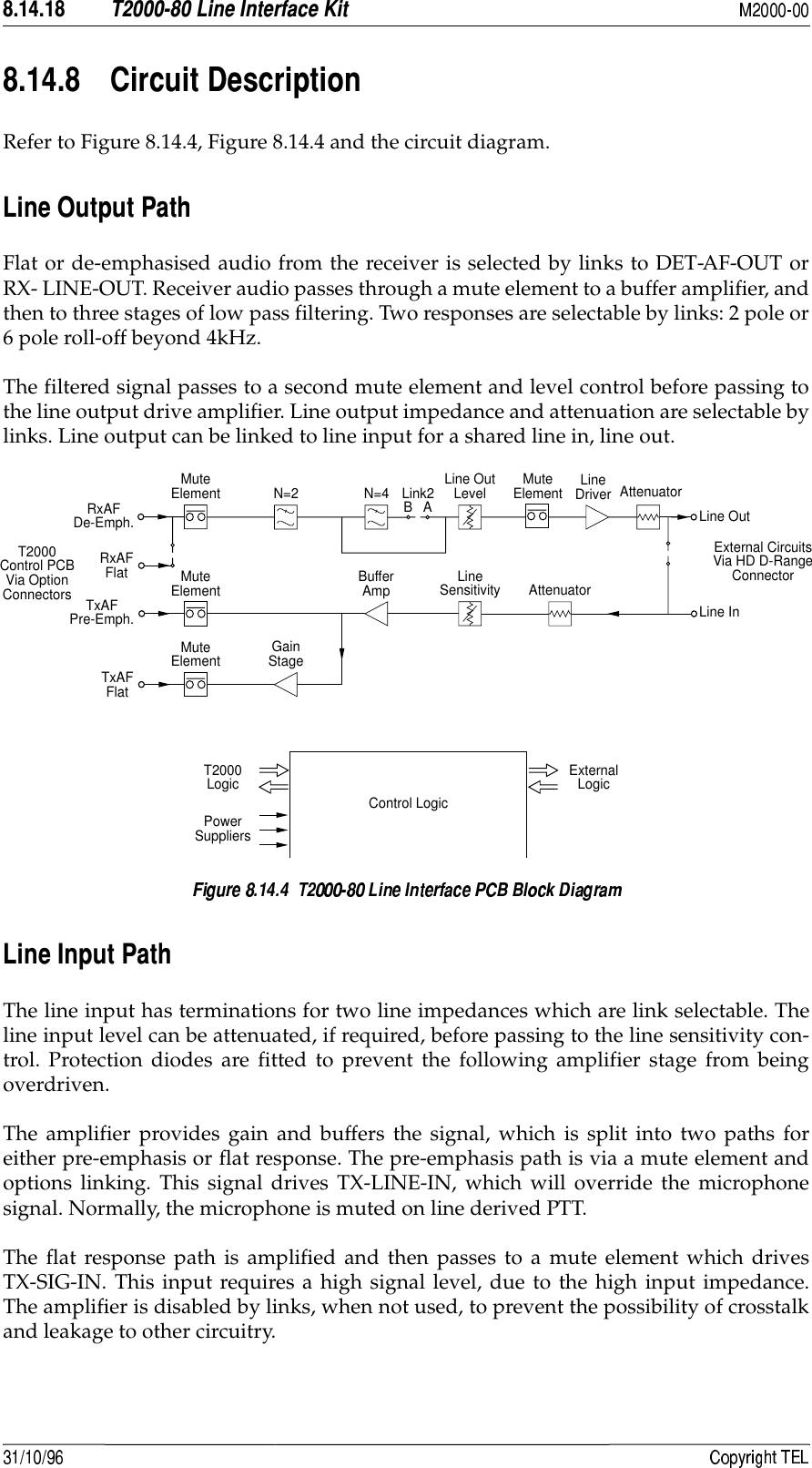
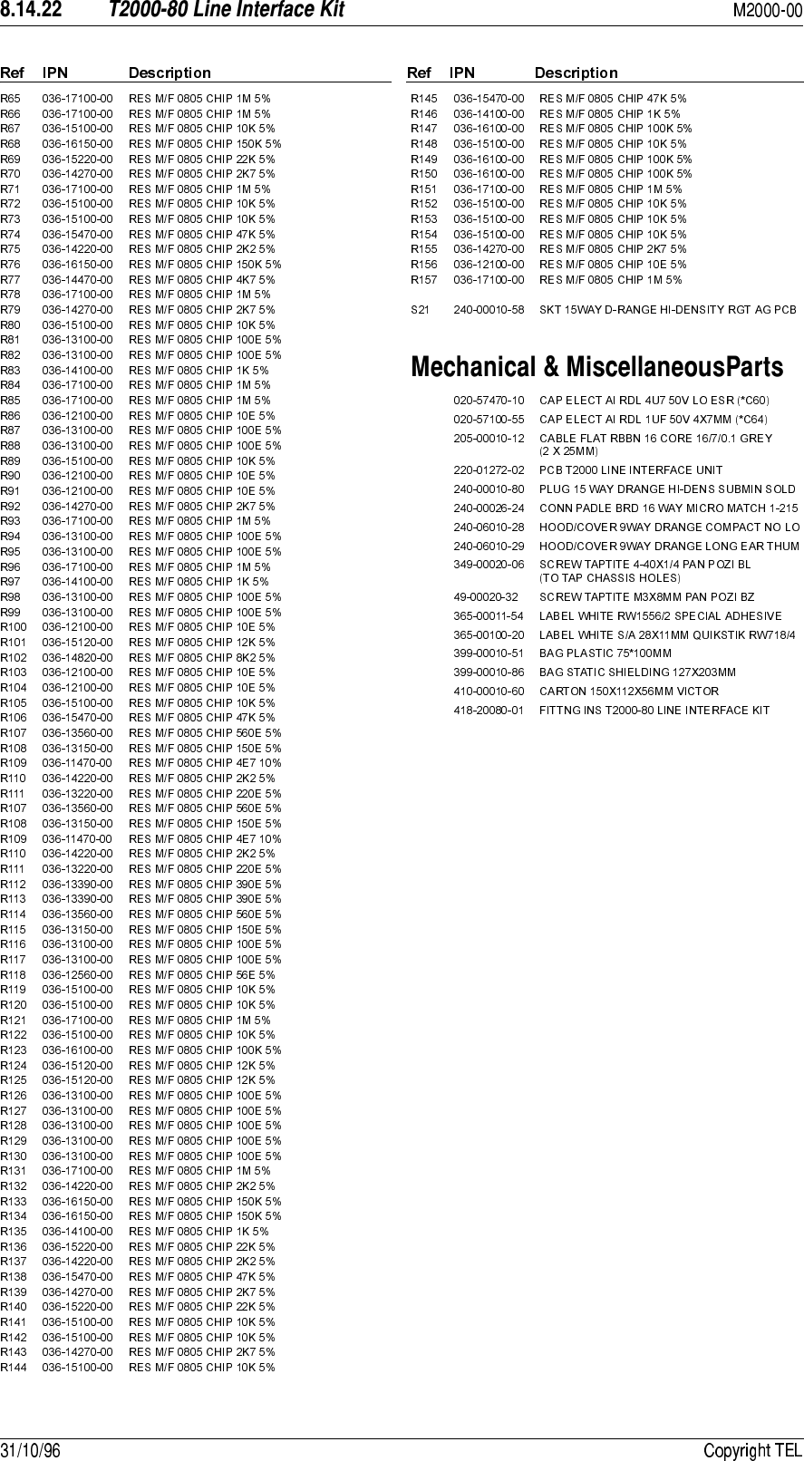
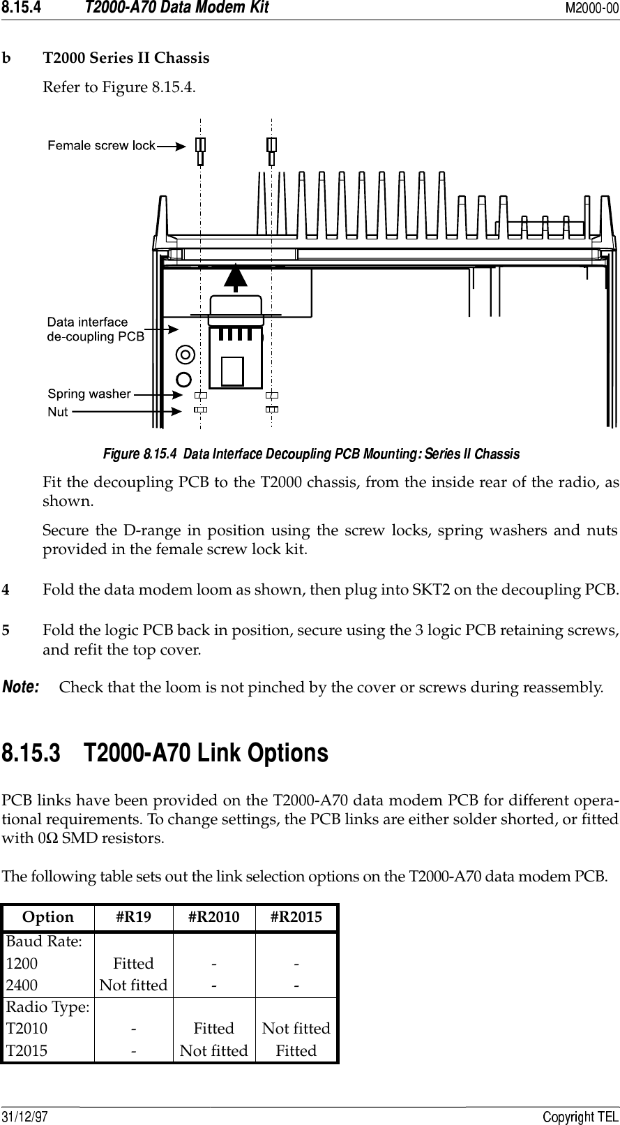
![ 673);41The adjustment section assumes that the T2000 radio has been correctly alignedfor normal operation. Refer to Section 8.14.3, “Line Interface Options” and the cir-cuit diagram for linking and application details.2If the logic and T2000-80 PCBs are unscrewed and folded out for adjustment, awire should be temporarily fitted from the radio chassis to the options chassisground pad (S35), as shown in Figure 8.14.1.3Signals for balanced transmissions are generally less than 0dBm, and are typicallybetween -10dBm and -20dBm.4Ensure that the LED is on ( LED on trunking radios). Deviation settings are given first for wide band radios, followed by settings fornarrow band radios in brackets [ ].##,1Ensure that the LED is on ( LED on trunked radios).2Monitor the line output (S21 pin 5).Apply an on channel signal from the RF signal generator at an output level of-70dBm, modulated to ±3kHz [±1.5kHz] deviation, at 1kHz AF.Adjust the RV1 (line output control) for the required output level. If the line output level is to be less than -15dBm, short LINK6 (600Ω output) andremove LINK5, to select 15dB of attenuation.#,1Monitor the line input (S21 pin 15). Ensure the indicator is off, and key the transmitter via the opto input (+8V).2Adjust RV2 (line input sensitivity control) until ±3kHz [±1.5kHz] deviation at1kHz is achieved. For input signals of greater than -15dBm, set the line input attenuation for 15dB(LINK11 open).7!This circuit delays audio gate turn on after PTT, to prevent squelch noise bursts inrepeater applications. 1Enable the time delay circuit by solder shorting LINK23. 2Set the required time delay using RV3 (time delay control).FnFn](https://usermanual.wiki/Tait/T2010-313.user-manual-part-6/User-Guide-356951-Page-30.png)
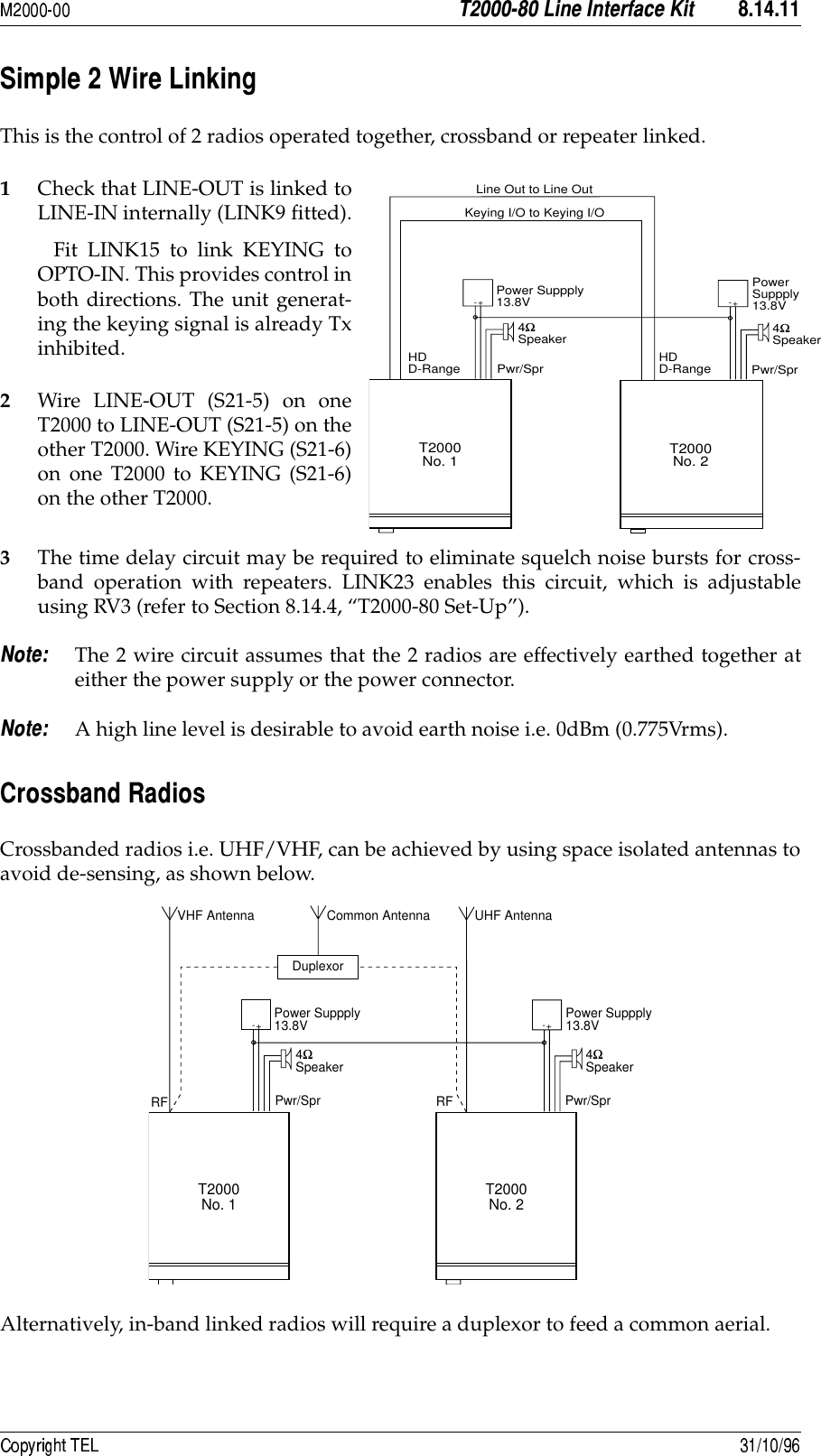
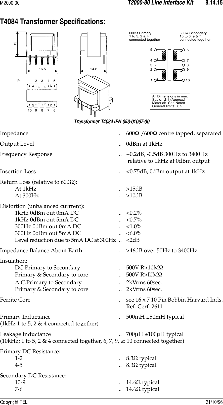
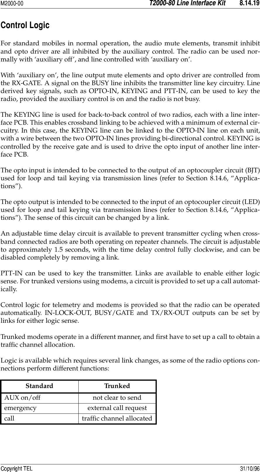
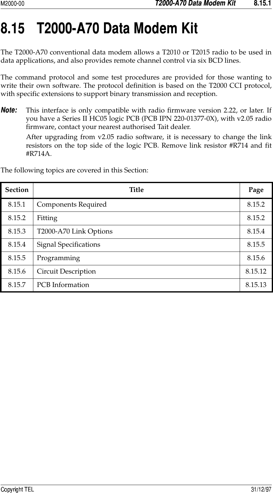
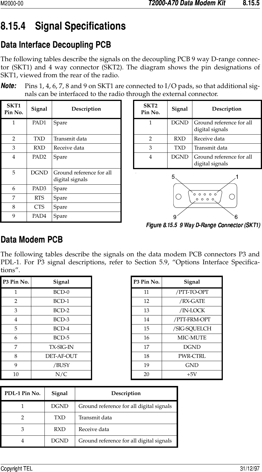
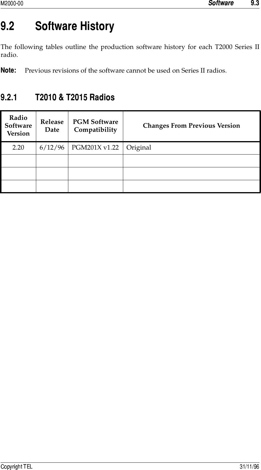
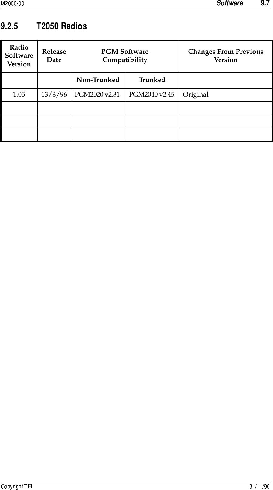
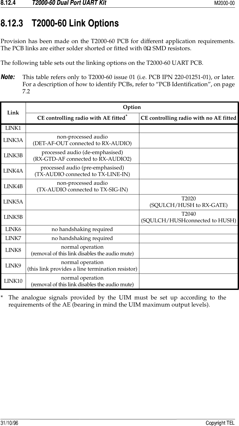
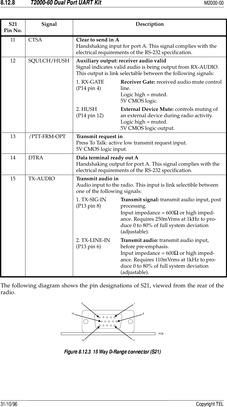
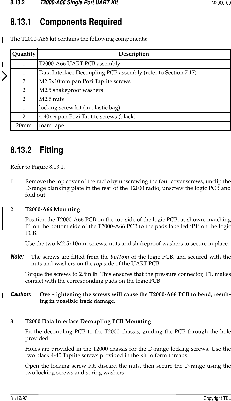
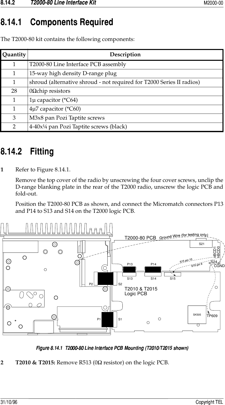
![#*2') +'&.All message packets take the general form:[IDENT][SIZE][PARAMETERS][CHECKSUM]<CR>The following table explains each component of the message packet.General message format characteristics:• All fields in a message are encoded in ASCII, except for the [PARAMETERS] field ofthe transmit and receive commands, which is encoded in Binary.• Where numeric values are represented in ASCII-hex notation (two characters perbyte), digits A to F are upper case.• The minimum length of a command packet is 5 characters (i.e. this is when [SIZE] =00).• The maximum length of the [PARAMETERS] field is 111 characters. The maximumlength of the command packet is therefore 116 characters ([SIZE] = 0x6F).Message Component Description[IDENT] The message identifier. Identifiers are single ASCII characters (lower-case alphabetical) which categorise the message type.[SIZE] The number of characters which make up the [PARAMETERS] field. [SIZE]is an 8-bit number expressed in ASCII-hex notation (two characters).[PARAMETERS] An optional field, depending upon the command. Parameter values are generally character strings, unless explicitly stated otherwise. Parameter type is dependent upon the command - there is no explicit type definition.[CHECKSUM] An 8 bit checksum of fields [IDENT],[SIZE] and [PARAMETERS]. It is expressed in ASCII-hex notation (two characters).Calculating [CHECKSUM]:[CHECKSUM] is calculated by applying the following algorithm:1Take the modulo-2 sum of all message bytes preceding [CHECKSUM].2Retain bits 0 to 7, discarding any higher order bits resulting from the summation.3Form the two’s complement of the remainder.4Convert the binary number into two ASCII-hex digits, MSD first.<CR> The packet terminator. It is the ASCII “carriage return” character ($0D).](https://usermanual.wiki/Tait/T2010-313.user-manual-part-6/User-Guide-356951-Page-55.png)
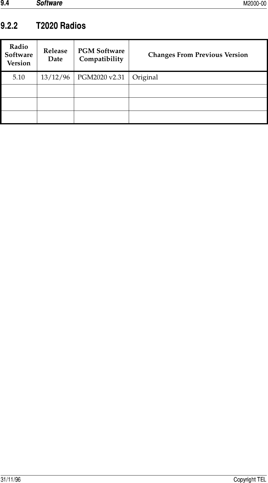
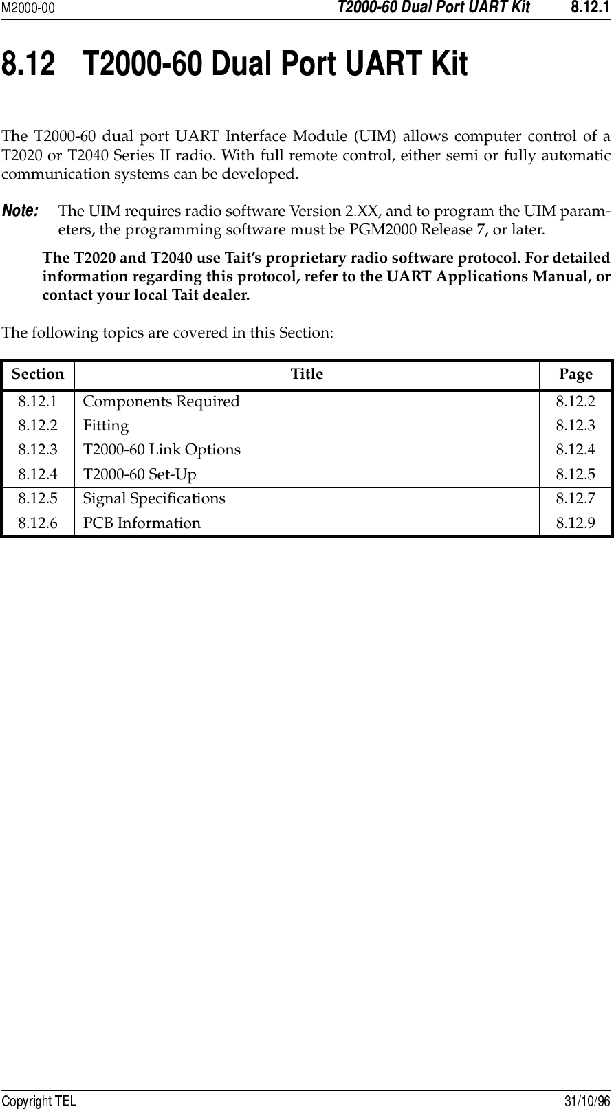
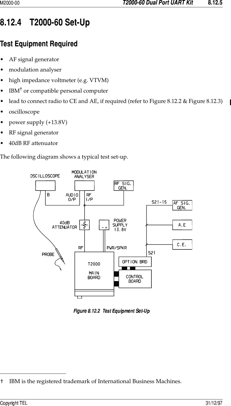
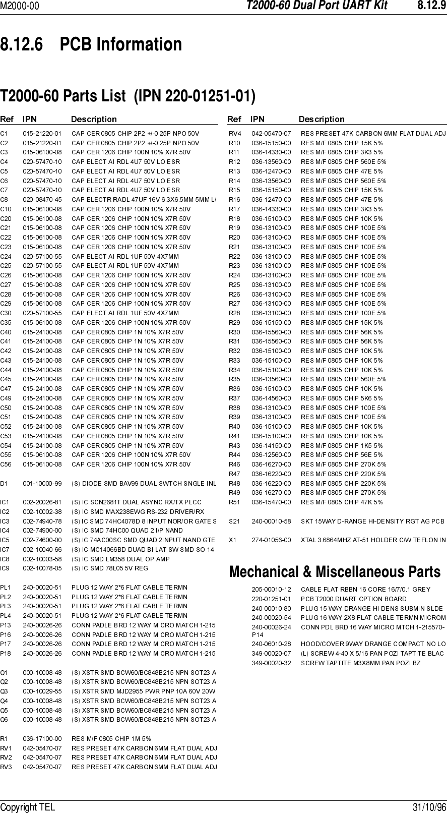
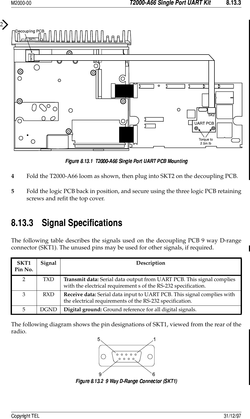
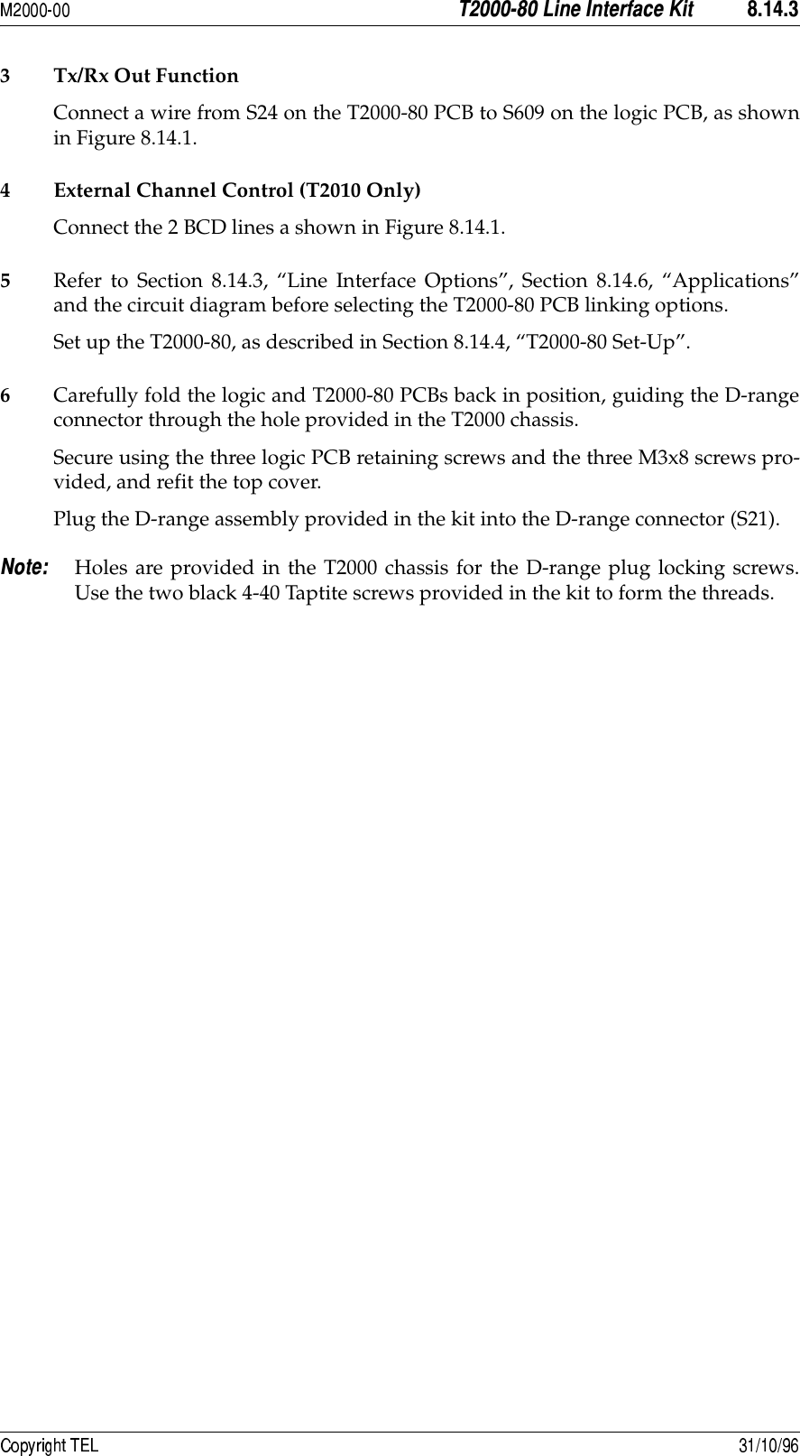
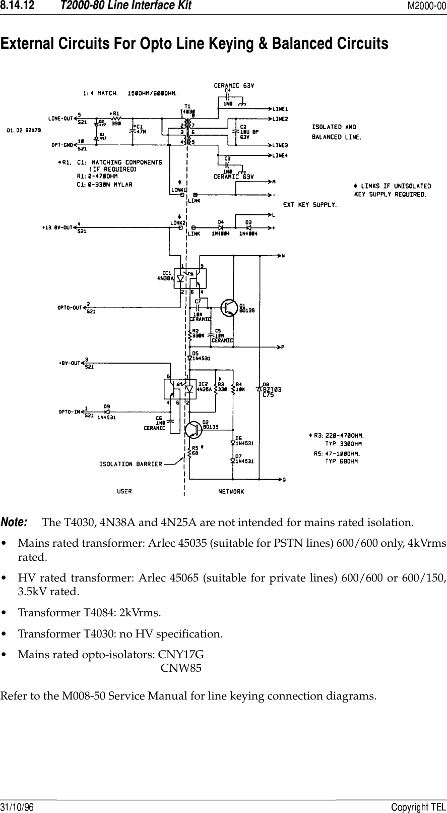
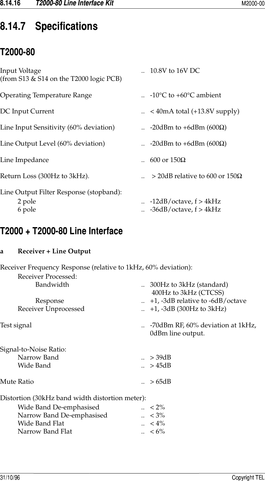
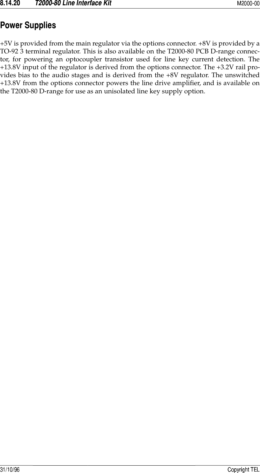
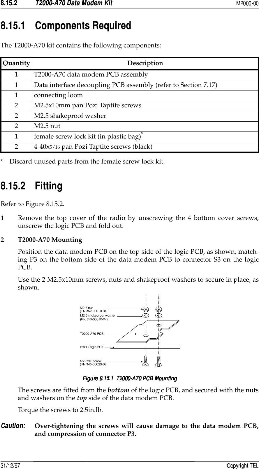
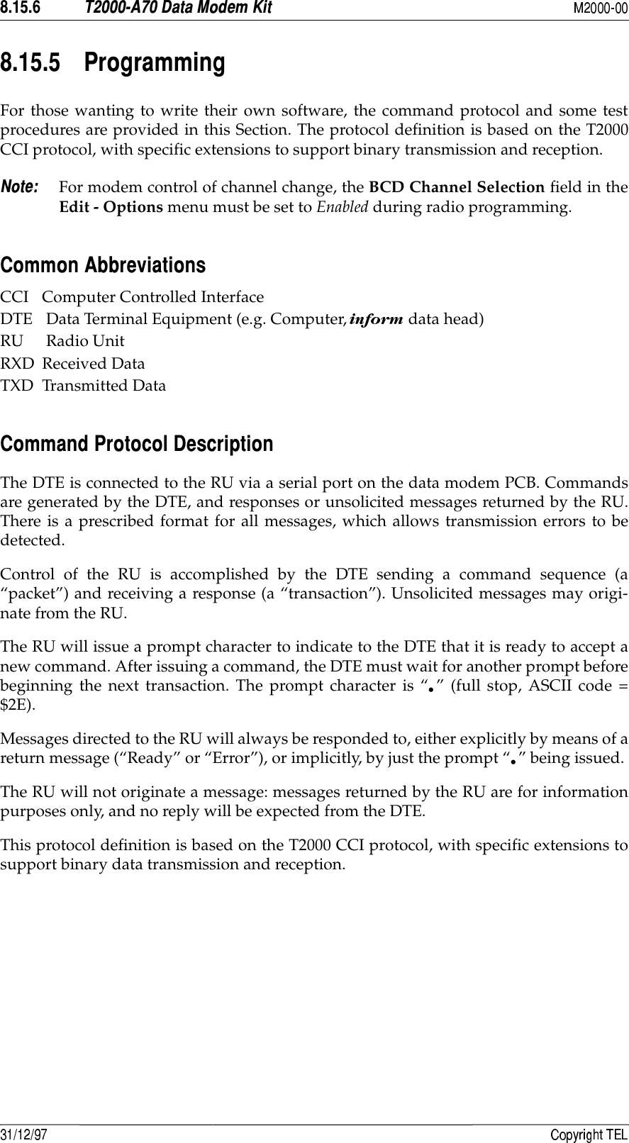
![ #*2')'&$)4If the RU receives a command without error, and all parameters are valid, then the com-mand will be executed and an acknowledge will be returned to the DTE. If an errorarises, the DTE will be notified with an appropriate response.The following Table describes the commands available to the DTE to control operationof the RU.Command Description Message Comments[IDENT] [PARAMETERS]Go To Channel This forces the RU to change to another (conventional) chan-nel.g [CHANNEL NUMBER]This is a string of characters representing the new channel number. The range of allowed characters is 0 to 9 only, and the maximum number of dig-its is 3. Valid channel numbers are 1 to [NUM CHANNELS].The value of [CHANNEL NUMBER] must be valid for the RU being control-led. The range of allowed values depends upon the RU’s programming, type and the link selections on the data modem PCB (refer to Section 8.15.3). The maximum allowable value is returned by the ‘Query’ command.Query This requests the RU to respond with a block of data identifying the type of RU attached, and the version of modem firmware.qNone The Query data is returned to the DTE as a ‘Query Response’ message (refer to “Messages from the RU”).Transmit This requests the RU to broadcast a block of data on the radio chan-nel.bThe data to broadcast is encoded as binary data. Note that this field may contain unprintable ASCII characters (such as CR/LF) and protocol command characters (such as “•”).The maximum length of data that may be sent with the ‘Transmit’ command is 111 characters.Null This requests the RU to return an acknowl-edgement to the DTE. The DTE can use this command to check that an RU is connected.nNone](https://usermanual.wiki/Tait/T2010-313.user-manual-part-6/User-Guide-356951-Page-56.png)
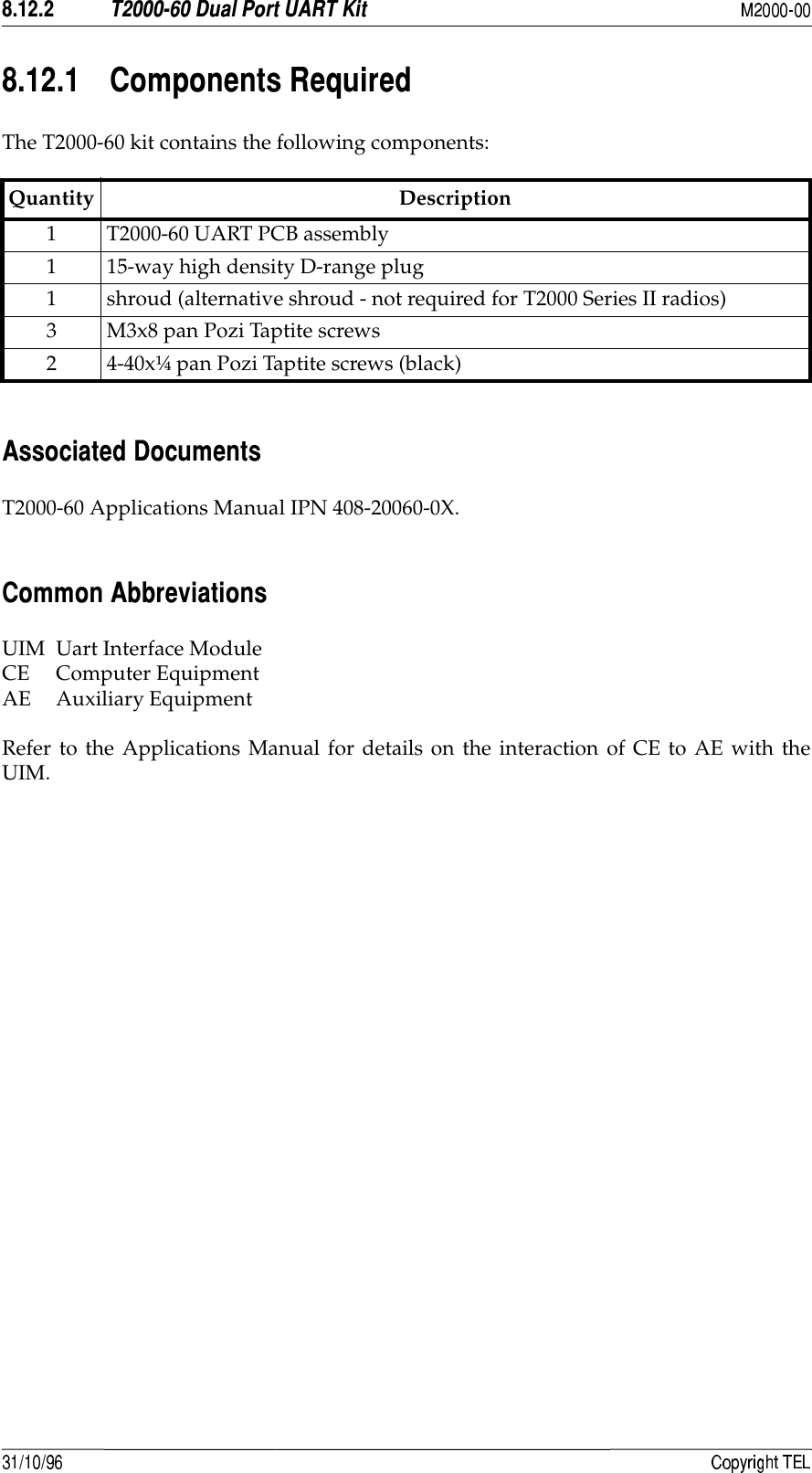
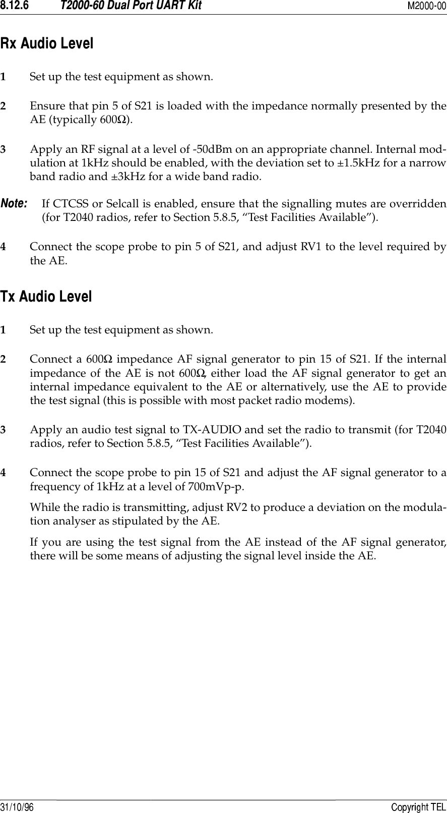
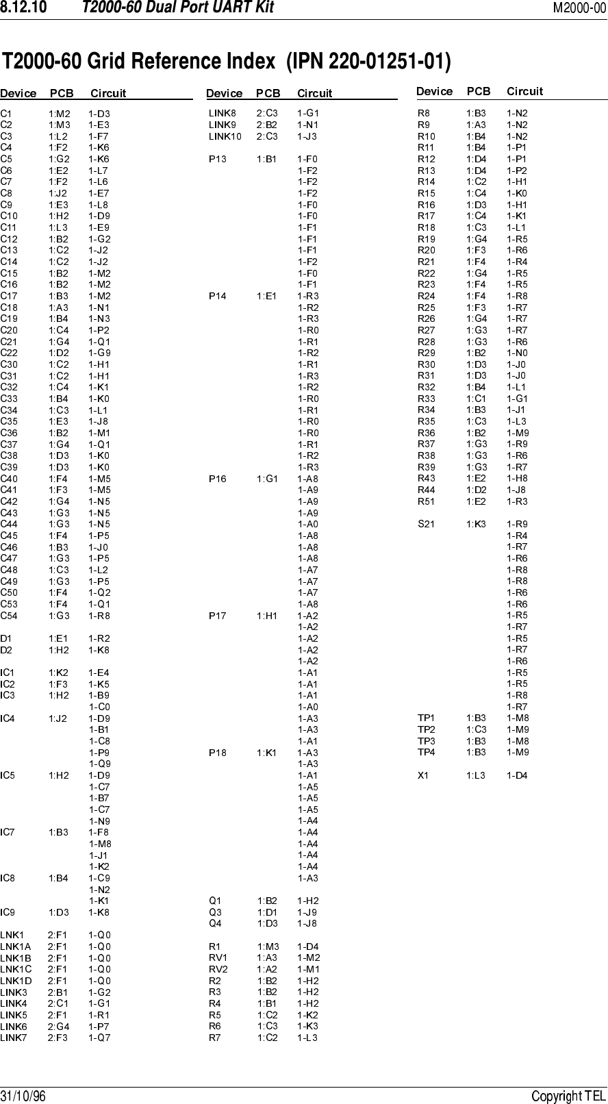
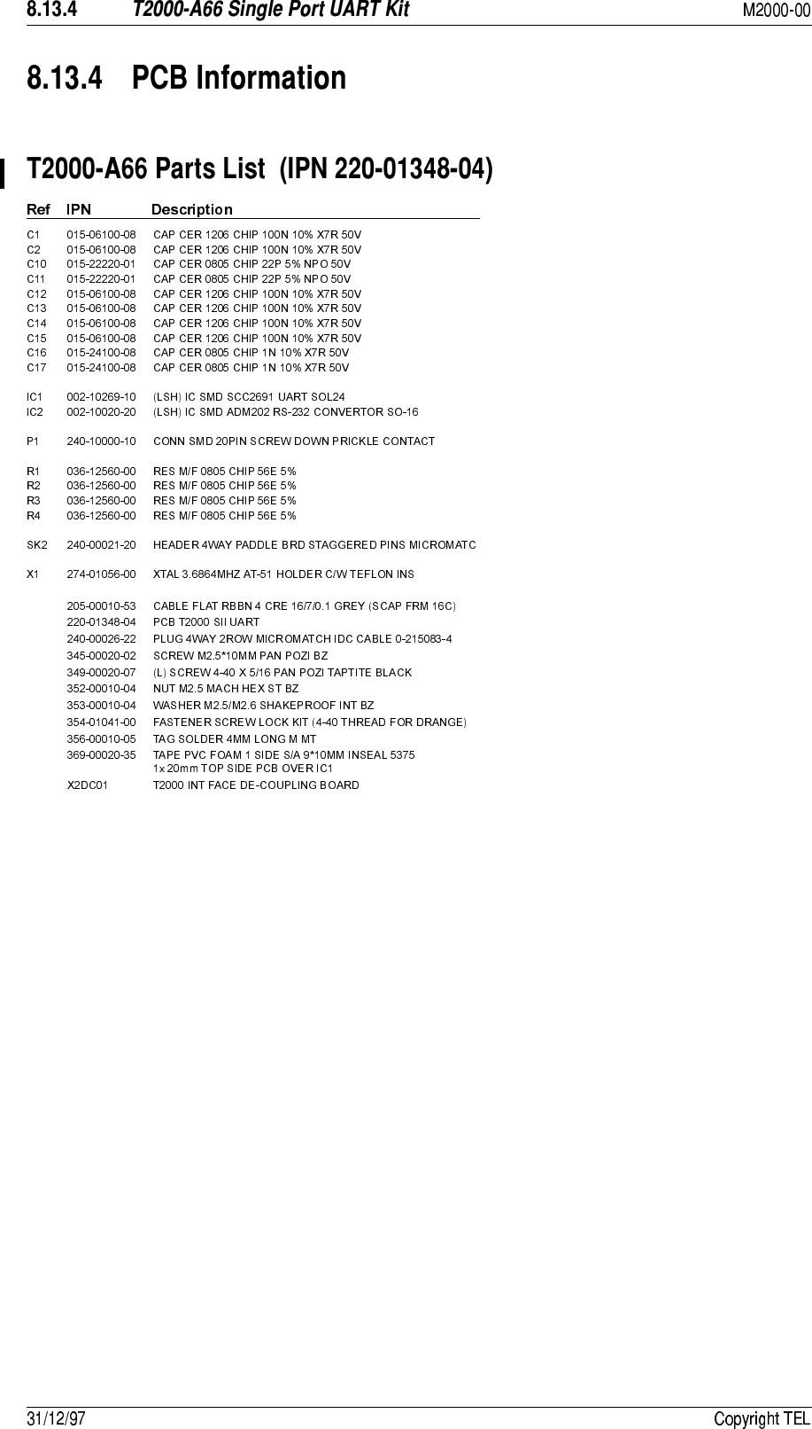
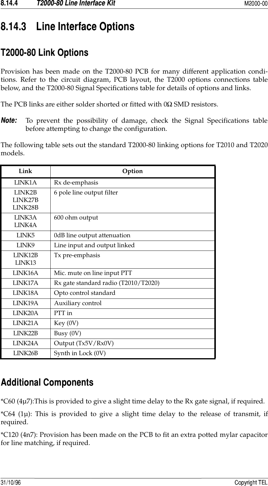
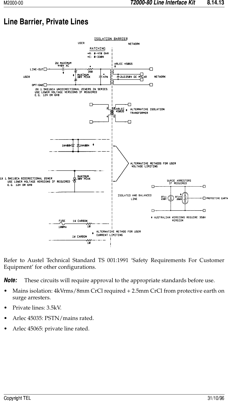
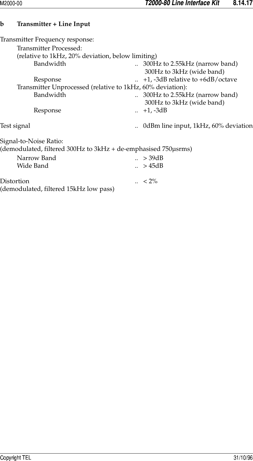
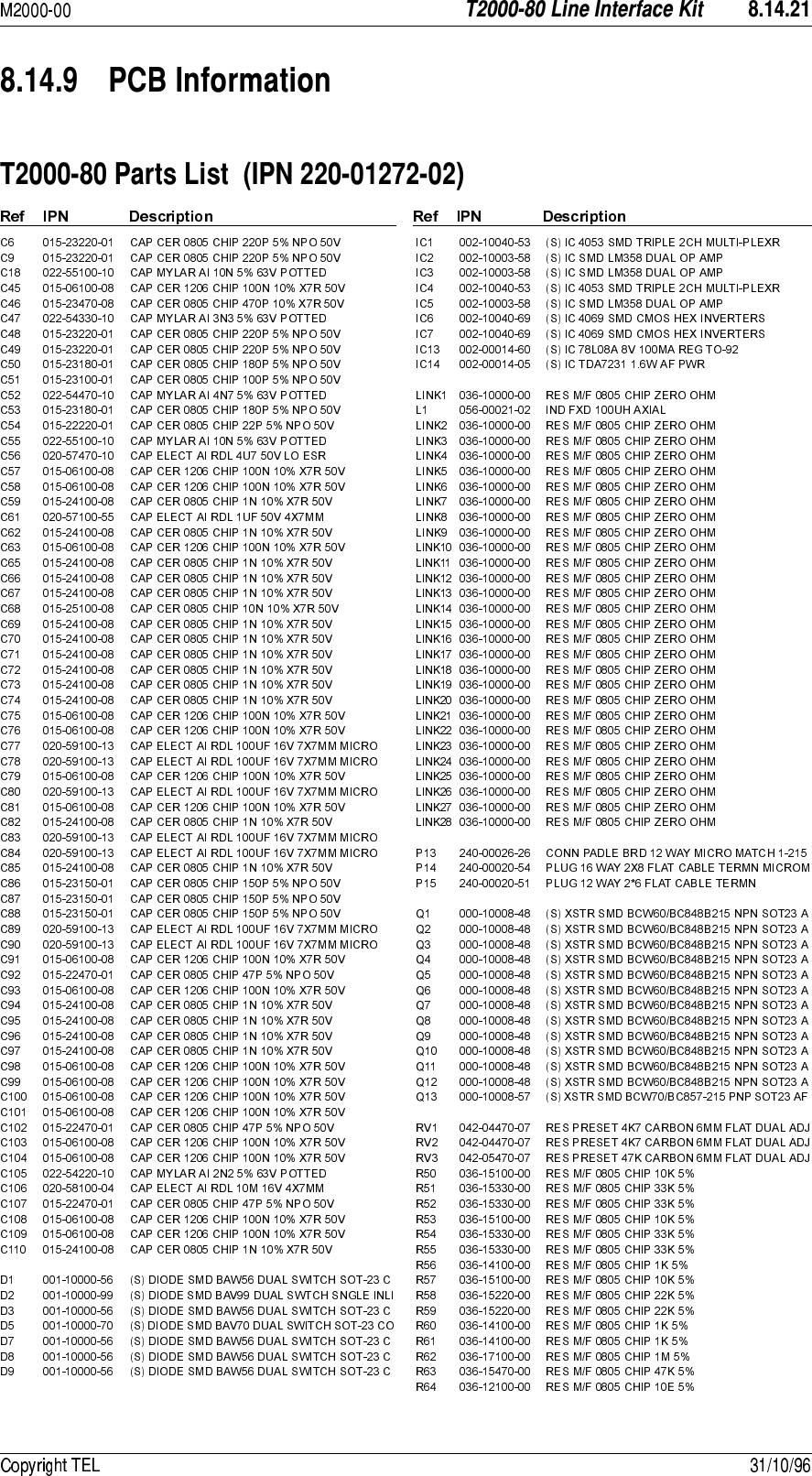
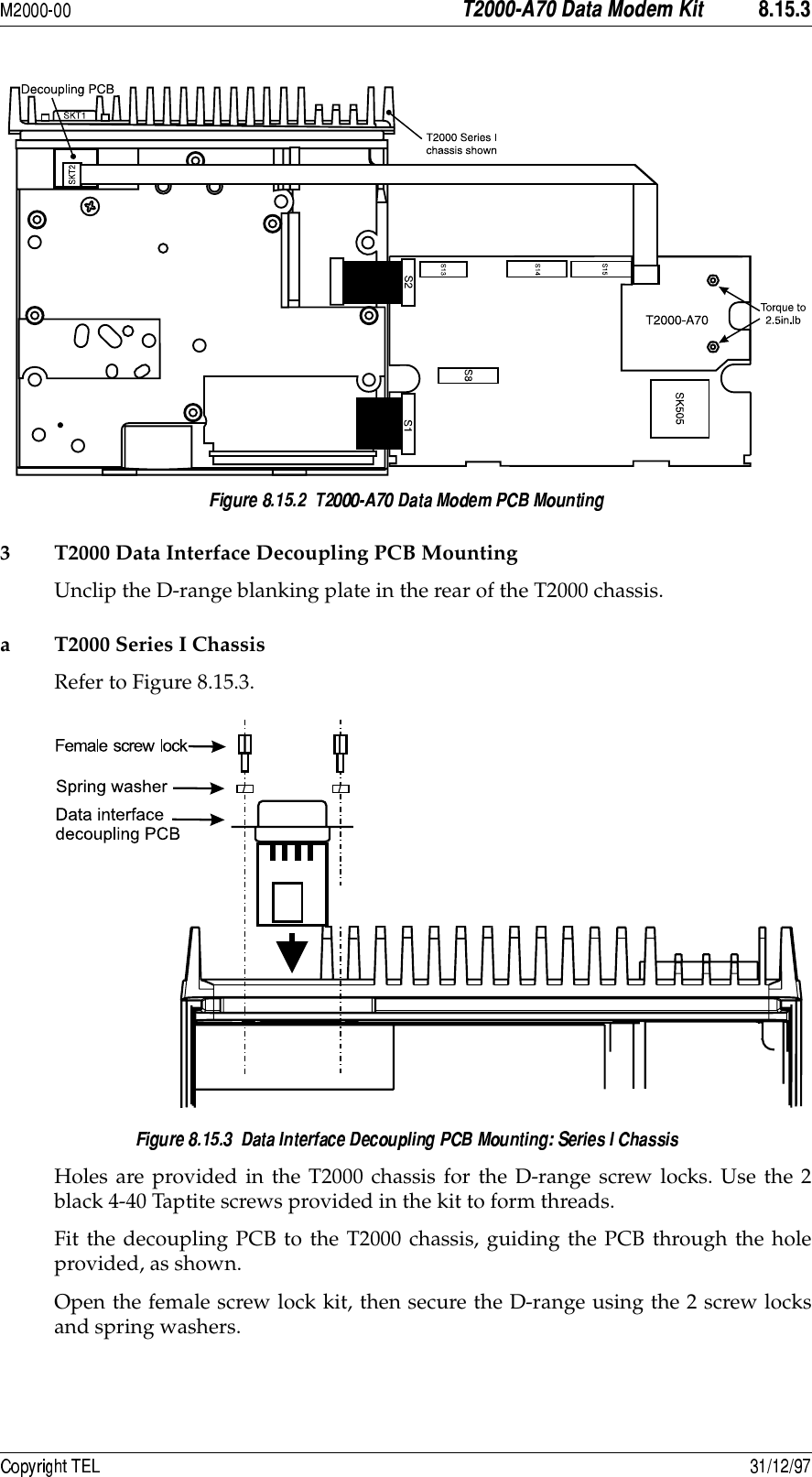
![#*2') -'&.$)4Messages may be sent to the DTE by the radio as part of a transaction (i.e. in response toa command issued by the DTE) or unsolicited. In the case of solicited commands, theprompt character will be issued after the RU response to terminate the transaction andsignify that another may begin. In the case of solicited commands, the prompt character, “•”, will be issued after theRU response, to terminate the transaction and signify that another may begin.Unsolicited commands from the RU will not cause the issuing of the promptcharacter, as it is possible for an unsolicited command (e.g. Receive) to occurduring a solicited command (e.g. Transmit).The following Table describes messages from the RU to the DTE.Command Description Message Comments[IDENT] [PARAMETERS]Receive Unsolicited.This presents data received by the RU to the DTE. The data received by the RU has been broadcast by another RU/DTE, using the Transmit command.i The data received is encoded as binary data. Note that this field may contain unprintable ASCII characters (such as CR/LF) and protocol command characters (such as ‘•’).QueryResponse SolicitedThe RU’s response to a Query command.m[RU TYPE] A single character, representing the model of the RU.0 = unknown3 = T20104 = T20151The value of [PVER-SION] = 1.01 is reserved for the first release of firmware implementing this command protocol. Subsequent enhance-ments and major upgrades will incre-ment this number accordingly.2Additional fields may be added to this message in future releases to pro-vide more information about the RU environ-ment. In particular, it may be necessary to pass the DTE some information on how the RU has been pro-grammed, or what optional hardware is fit-ted.[VERSION] Firmware version. A character string, in the format of X.XX, identifying the capabilities of the RU/modem.[PVERSION] Protocol Version. A character string, in the format of X.XX, identifying the com-mand protocol ver-sion supported.[NUMCHANNELS] The number of channels supported by the Go To Chan-nel command. A 3 digit ASCII number.Ready “•”This response indi-cates that a transac-tion has been completed, and the RU is ready for the next command.None None After issuing a command, the DTE must wait for another prompt before beginning the next transac-tion.Continued on next page](https://usermanual.wiki/Tait/T2010-313.user-manual-part-6/User-Guide-356951-Page-57.png)
![ #*2')Error Solicited response to a transaction error.This advises the DTE that the RU has detected an error condition and cannot proceed with the current transaction.Unsolicited response to a system error.In some cases, an exception condition in the RU may cause an ‘Error’ message to be sent to the DTE independently of any control transac-tions. A prompt or ‘Ready’ will be issued after an ‘Error’ occurs, to indicate the RU's availability to accept further commands.e[ETYPE] Error type. A single character represent-ing the error cate-gory.0 = transaction error. This indicates some problem with com-munications. All such errors result in the transaction being terminated, without the current command being executed.Transition error numbers ([ETYPE] = 0):1 0x01 = unsupported command errorThis may arise when the DTE expects a later version of RU than is attached, and attempts to use a command which is not recognised by the RU.2 0x02 = checksum errorindicates that the check-sum calculated by the RU did not match the one received in the com-mand packet.3 0x03 = parameter errorThis encompasses val-ues out of range, or missing fields.4 0x10 = communication failureThis encompasses all low level mechanisms, i.e. framing error, over-run error, parity error etc.5 0x20 = invalid channel numberThis may arise when the DTE issues a ‘Go To Channel’ command with a [CHANNEL NUMBER] exceeding the maximum allowable number.[ENUM] Error number. A character string rep-resenting a decimal number in the range of 00 to 99, which can identify the specific error condition.For [ETYPE] = 0, 01 = unsupported command02 = checksum error03 = parameter error10 = communica-tion failure20 = invalid channel numberCommand Description Message Comments[IDENT] [PARAMETERS]](https://usermanual.wiki/Tait/T2010-313.user-manual-part-6/User-Guide-356951-Page-58.png)
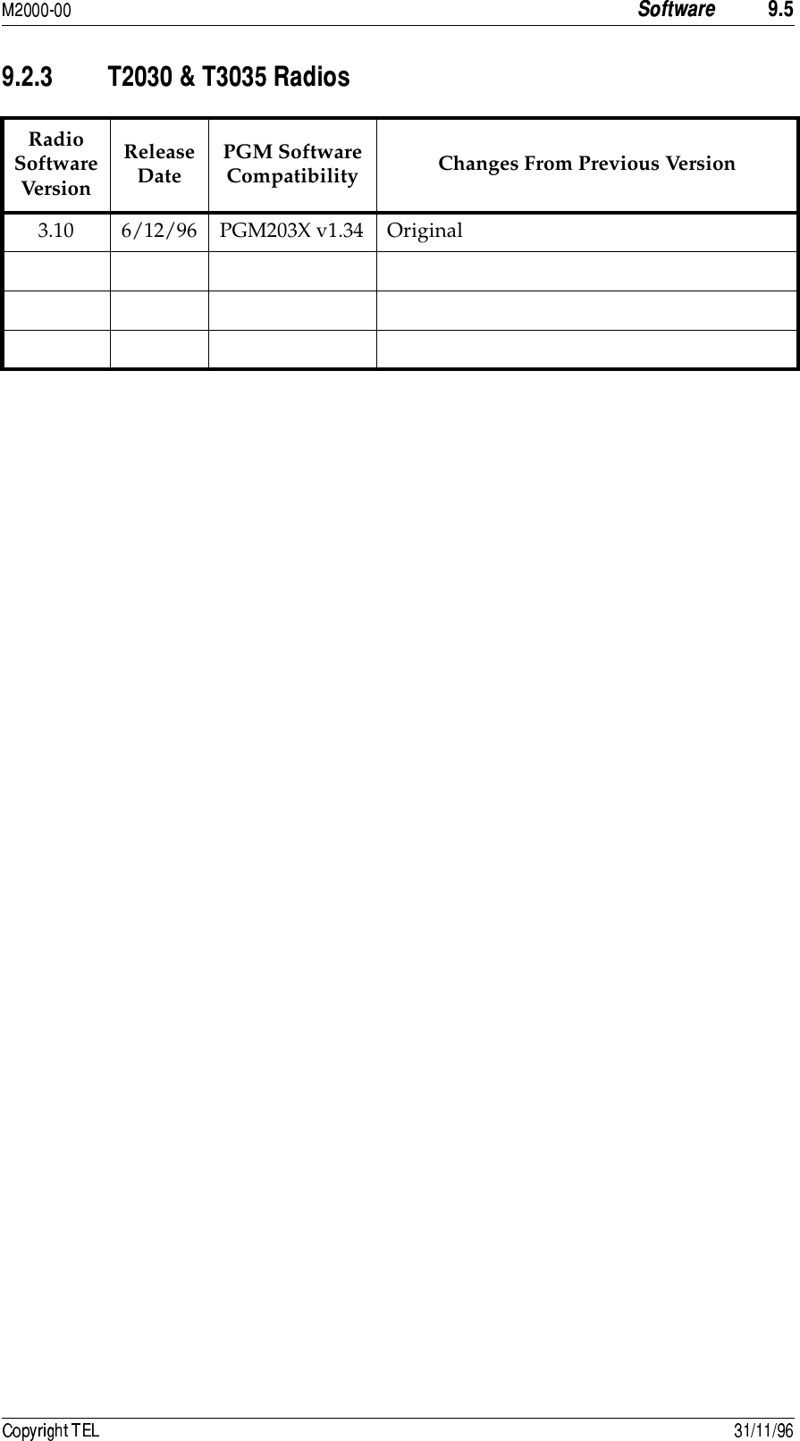
![#*2') The following Table explains the commands that may be sent to test the software.Command Test Procedure Expected ResultGo To Channel 1. Send command “g01206” Radio changes channel to 2, then returns the command prompt.2. Send command “g0203D4” Radio changes channel to 3, then returns the command prompt. 3. Send command “g03004A2” Radio changes channel to 4, then returns the command prompt.4. Send command “g0225D0” Radio sends error message “e03020A6” (invalid channel)Transmit 1. Send command “b04this82” Radio transmits this data and “i04this7B” is received by the other radio.2. Send command “b17This is a test command.14” Radio transmits this data and “i17This is a test command.0D” is received by the other radio. 3. Send a “b” command while the PTT is pressed. Radio sends error message ”e03010A7” (communication error)4. Send a command while the busy led is lit Radio sends error message “e03010A7” (communication error)Null Send command “n0032” Radio returns a prompt (“•”).Query Send command “q002F” T2010: a valid message could be “m0C31.011.01004D9” i.e.[RU TYPE] = T2010, [VERSION] = 1.01[PVERSION] = 1.01[NUM CHANNELS] = 04T2015: a valid message could be “m0C41.011.01024D6” [RU TYPE] = T2015, [VERSION] = 1.01[PVERSION] = 1.01[NUM CHANNELS] = 24Command Line Errors 1. Send command ”b03this83” Radio sends error message “e03003A5” (parameter error).2. Send command “b04this83” Radio sends error message “e03002A6” (checksum error).3. Send command “t04this70” Radio sends error message “e03001A7” (unsupported command).](https://usermanual.wiki/Tait/T2010-313.user-manual-part-6/User-Guide-356951-Page-59.png)