Tait TEL0033 Base Station Transmitter User Manual 8c500 bk
Tait Limited Base Station Transmitter 8c500 bk
UserManual.wiki
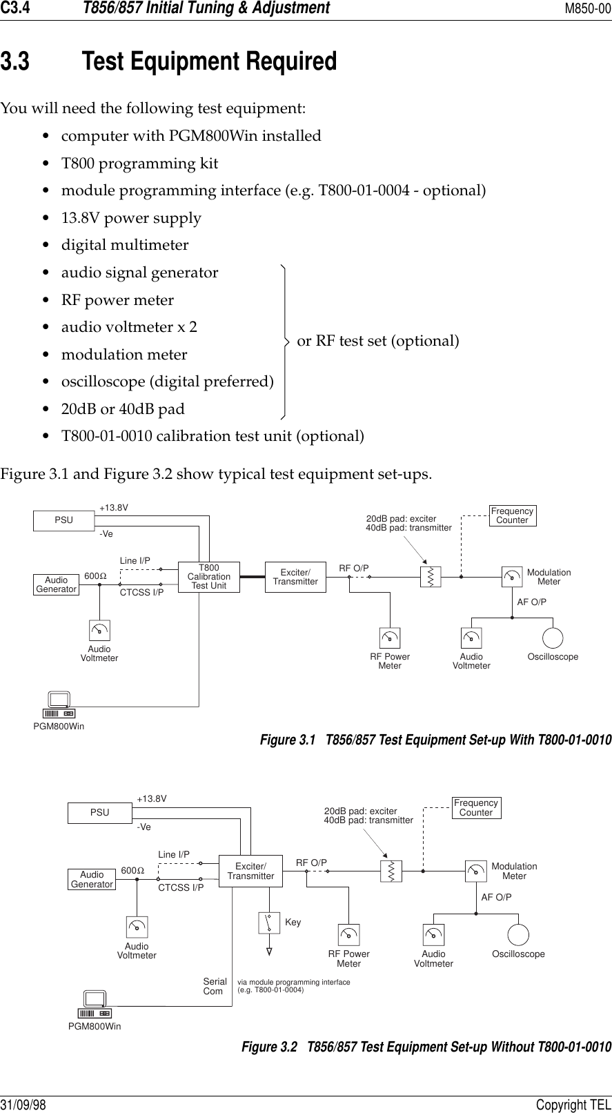
>
Tait
>
TEL0033 User Manual
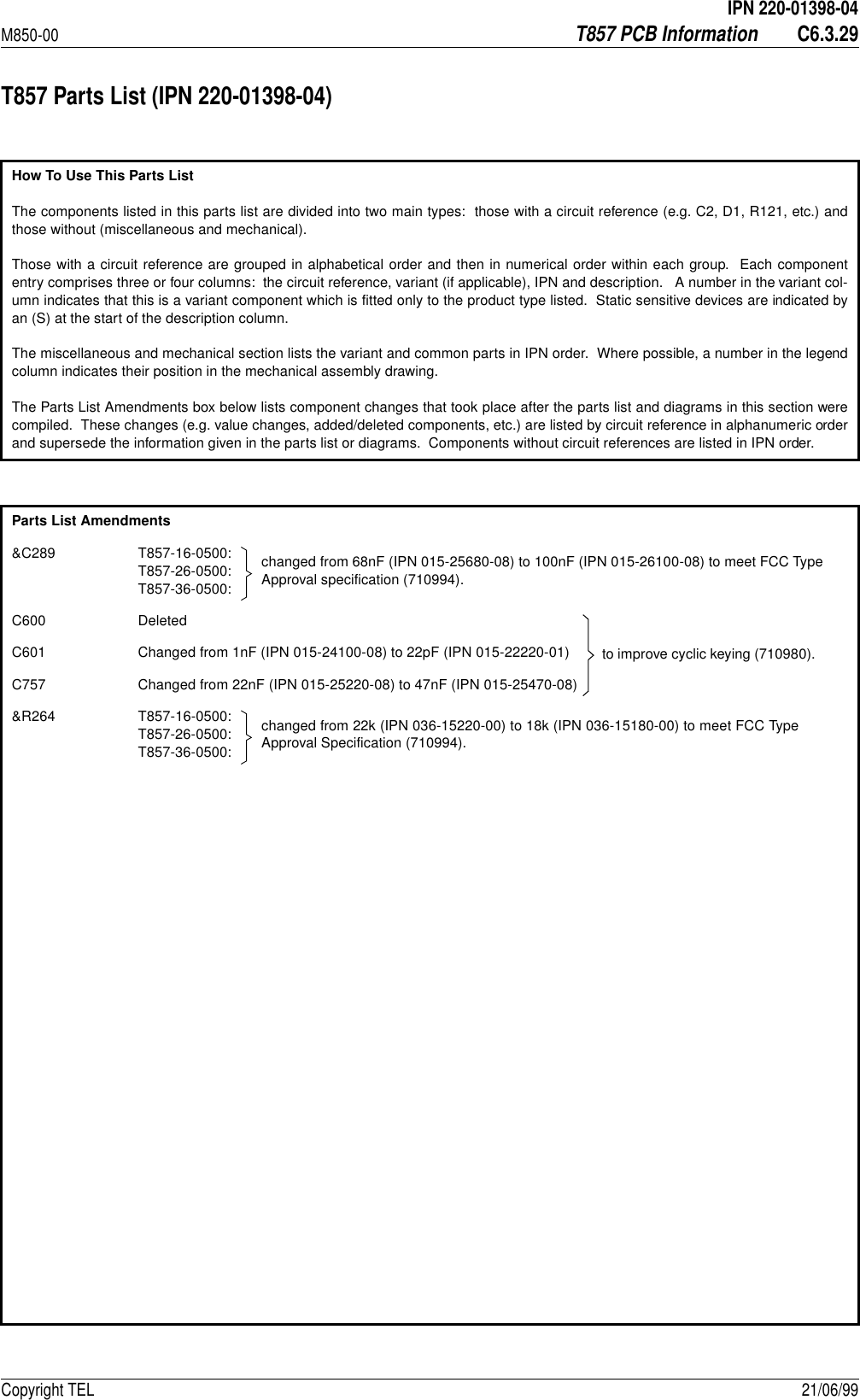
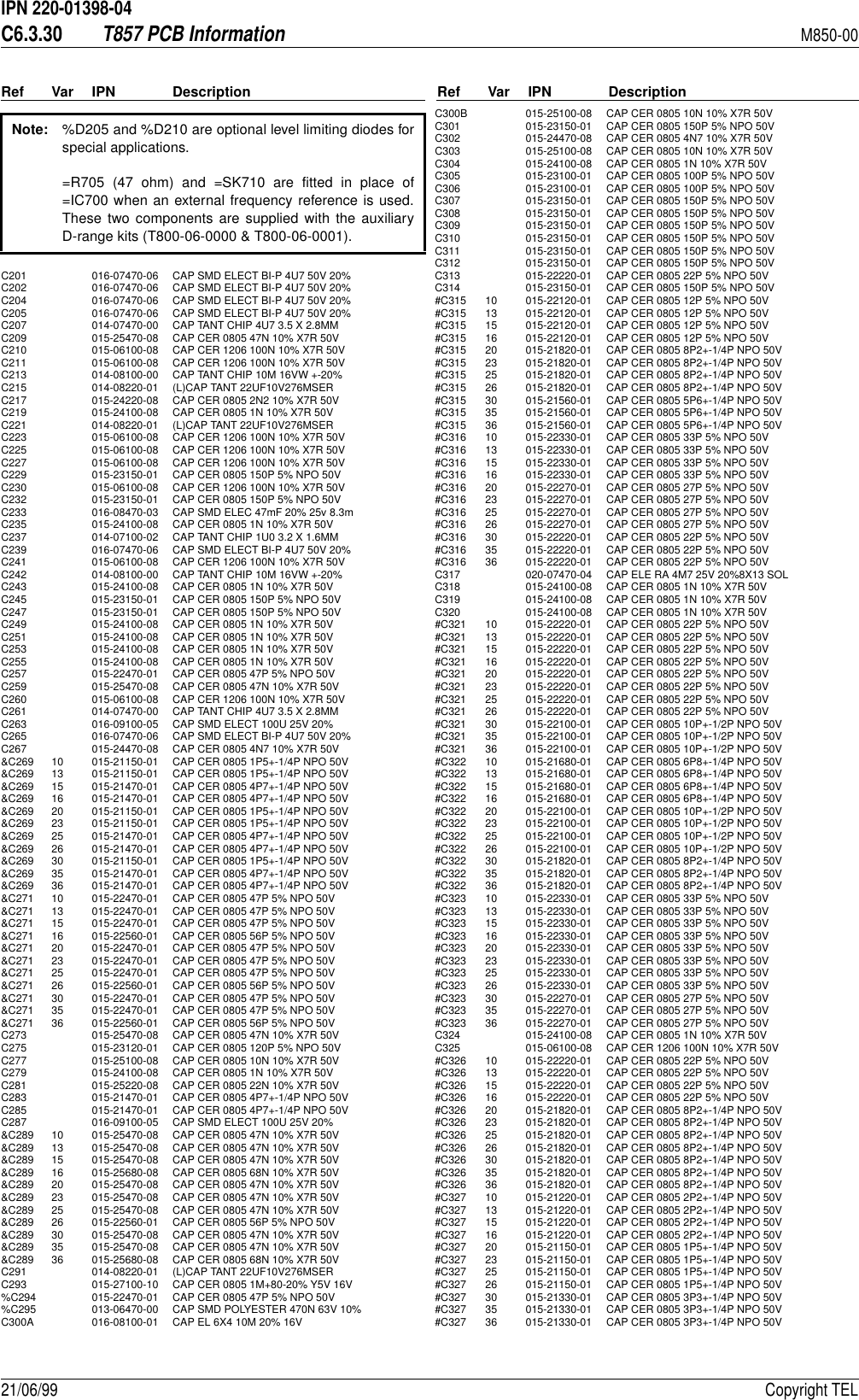
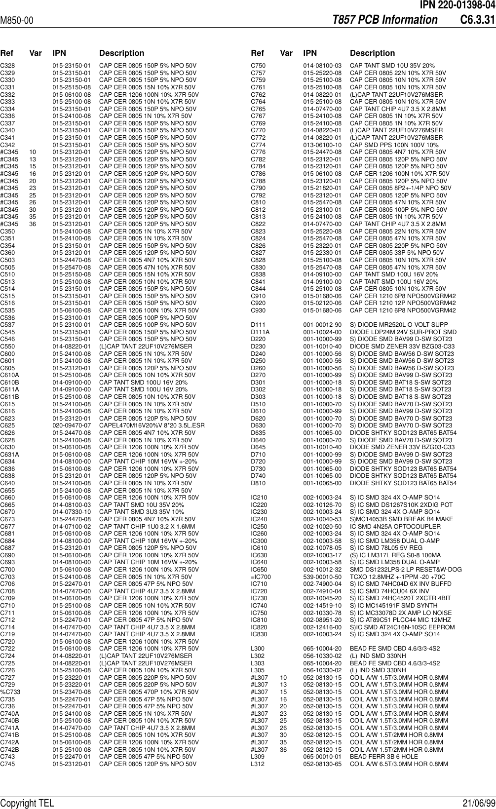
Cct Description Part List Manual
Navigation menu
Upload a User Manual
Namespaces
Wiki Guide
HTML
PDF
Info
Views
User Manual
Discussion / Help
Navigation


![M850-00T856/857 General InformationC1.11Copyright TEL 31/01/991.2.4.2 Modulation CharacteristicsFrequency Response .. flat or pre-emphasised (optional) (below limiting)Line And Microphone Inputs: Pre-emphasised Response- Bandwidth .. 300Hz to 3kHz (WB & MB).. 300Hz to 2.55kHz (NB)Below Limiting .. within +1, -3dB of a 6dB/octavepre-emphasis characteristic Flat Response .. within +1, -2dB of output at 1kHzAbove Limiting Response .. within +1, -2dB of a flat response(ref. 1kHz)Distortion .. 2%Hum And Noise: Wide Bandwidth .. -55dB (300Hz to 3kHz [EIA]) typical Mid Bandwidth .. -54dB (CEPT)Narrow Bandwidth .. -50dB (CEPT) Compressor (optional): Attack Time .. 10ms Decay Time .. 800ms Range .. 50dB1.2.4.3 CTCSSStandard Tones .. all 37 EIA group A, B and C tonesplus 13 commonly used tonesFrequency Error .. 0.08% max.(from EIA tones)Generated Tone Distortion .. 1.2% max.Generated Tone Flatness .. flat across 67 to 250.3Hz to within 1dBModulation Level .. adjustableModulated Distortion .. <5%1.2.5 MicrocontrollerAuxiliary Ports:Open Drain Type .. capable of sinking 2.25mA via 2k2ΩVds max. .. 5V](https://usermanual.wiki/Tait/TEL0033/User-Guide-83794-Page-11.png)


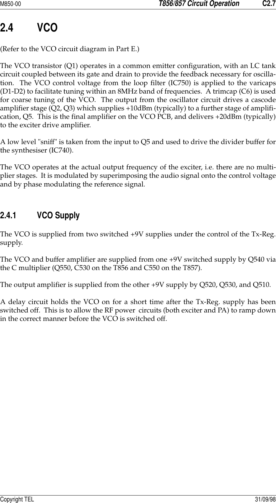
![M850-00T856/857 Circuit OperationC2.9Copyright TEL 31/09/982.5.3 Keying InputsThere are four ways to key the exciter: • pulling the Tx-Key line low (pin 13 on D-range 1 [PL100]) at the rear of the set);• pushing the "Carrier" button on the front panel - this will inhibit all audio;• using the PTT button on the local microphone, disabling audio from the line;• via the opto-key inputs (pins 11 and 12 on D-range 1 [PL100]) when electricalisolation is required. This features a constant current sink (Q270) to ensure reli-able activation of the opto-coupler (IC250) at low keying voltages.2.5.4 Compressor (Automatic Level Control (ALC))The input signal is fed via a current controlled attenuator (Q230, Q220) to a high gainstage (IC230) from which the output signal is taken. This signal is passed to a compara-tor (IC230) which toggles whenever the audio signal exceeds a DC threshold deter-mined by RV220. Thus, the comparator produces a square wave whose mark-spaceratio is determined by the amplitude of the audio signal. This square wave pumps upthe reservoir capacitor (C233) which controls the attenuator (Q230, Q220), thus complet-ing the feedback loop.The compression level is set by adjustment of the comparator threshold (RV220).Note:Although the high dynamic range of the compressor allows the use of verylow audio signal levels, such conditions will be accompanied by a degrada-tion of the signal-to-noise ratio. Very low audio input levels should there-fore be avoided where possible.2.5.5 Outputs To ModulatorsThe output signal from the limiter (IC210, IC230) is summed with a CTCSS tone at asumming amplifier (IC260). The signal is then low pass filtered (IC260) and split to sup-ply the two modulators.Since the VCO modulator is a true frequency modulator, its audio is simply buffered(IC260). The reference modulator, however, is a phase modulator and its audio mustfirst be integrated (IC210).It is vital that the audio levels to the modulators are accurately set, relative to eachother. Hence the inclusion of level adjustment in the reference modulator path. Onceset, adjustments to absolute deviation may be made only via the deviation digital pot.(IC220 - adjustable via PGM800Win).](https://usermanual.wiki/Tait/TEL0033/User-Guide-83794-Page-25.png)

![C3.6T856/857 Initial Tuning & AdjustmentM850-0031/09/98 Copyright TEL3.4.4 Two Point Modulation AdjustmentNote 1:In this and following sections deviation settings are given first for widebandwidth sets, followed by settings in brackets for mid bandwidth sets ( )and narrow bandwidth sets [ ].Note 2:Reference modulation and limiter adjustment are controlled byPGM800Win. Electronic potentiometers (256 step) are used to allow chan-nel-by-channel adjustment of deviation and two point modulation.Note 3:To optimise the modulation response across the switching range, repeatsteps 1-4 below for each channel that will be used (usually needed only fordata applications). In applications where the modulation response is lesscritical (e.g. voice use only), carry out steps 1-4 below on the middle channeland cut and paste the value to all other channels.1. Inject an audio signal of 300Hz 1.5V rms (+5dBm) into the CTCSS input (D-range1 (PL100) pin 8). Key the transmitter by earthing the Tx-Key line.2. Adjust the output from the audio generator to obtain ±3kHz (±2.4kHz) [±1.5kHz]deviation at 300Hz.3. Change the input frequency to 100Hz and adjust IC220 via PGM800Win “refer-ence modulation” to obtain ±3kHz (±2.4kHz) [±1.5kHz] deviation (you can useeither the mouse or up and down arrow keys).4. Change the input frequency back to 300Hz.Repeat steps 2 and 3 above until the deviations achieved at the two input frequen-cies are within 0.2dB of each other. You will need to do this at least four times.5. Sweep the audio between 50 and 300Hz for peaks.Note:A peak between 50 and 300Hz will indicate a fault condition, i.e:- incorrect set-up or - modulation circuitry fault. The specification window is ±1dB relative to 150Hz from 67 to 260Hz.3.4.5 FM Deviation (Limiter) AdjustmentNote:If the T856/857 will be used over the whole 8MHz switching range, youmust set the deviation for each channel. However, if the module will beused on frequencies that cover only a 1MHz (or less) switching range, youcan set the deviation on the middle channel and use this value for all otherchannels with the “fill” option in PGM800Win.Inject 1kHz at -10dBm into the line input (D-range 1 (PL100) pins 1 & 4; pins 2 & 3shorted; refer to Section 2.2 of Part F).](https://usermanual.wiki/Tait/TEL0033/User-Guide-83794-Page-36.png)
![M850-00T856/857 Initial Tuning & AdjustmentC3.7Copyright TEL 31/09/98Adjust RV210 (line sensitivity) fully clockwise and key the transmitter by earthingthe Tx-Key line. Adjust IC220 via PGM800Win “deviation” to set the peak devia-tion to ±4.7kHz (±3.8kHz) [±2.3kHz] (you can use either the mouse or up anddown arrow keys).Sweep the audio frequency from 100Hz to 4kHz and ensure that the maximumdeviation does not exceed ±4.7kHz (±3.8kHz) [±2.3kHz]. Readjust IC220 if neces-sary via PGM800Win “deviation”.3.4.6 Line-in Level AdjustmentSet the injected signal at the line input to the required line level (typically -10 to-20dBm).Adjust RV210 (line sensitivity) to provide ±3kHz (±2.4kHz) [±1.5kHz] deviation.3.4.7 CTCSS EncoderProgram a CTCSS tone on the set channel using PGM800Win.Key the T856/857 with the front panel "Carrier" switch.Adjust RV805 (CTCSS level adjust) to give 10% system deviation.Reset the maximum deviation as per Section 3.4.5.](https://usermanual.wiki/Tait/TEL0033/User-Guide-83794-Page-37.png)
![C3.8T856/857 Initial Tuning & AdjustmentM850-0031/09/98 Copyright TEL3.5 Audio Processor Links3.5.1 Link DetailsUse the following table to set up the audio processor to the configuration you require.You should set the audio processor links before carrying out any of the tuning andadjustment procedures. The factory settings are shown in brackets [ ].3.5.2 Typical OptionsPlug Linkaa. The letters in this column and in the table in Section 3.5.2 below refer to the identificationletters screen printed onto the PCB beside each pair of pins.FunctionPL2051-2[3-4]5-6ABCnot connectedmicrophone pre-amp. output to compressor inputmicrophone pre-amp. output to multiplexer inputPL210[1-2]3-45-6LMNmultiplexer output to pre-emphasis inputmultiplexer output to limiter inputmultiplexer output to compressor inputPL2151-2[3-4]5-67-89-10GHIJKnot connectedcompressor output to multiplexer inputcompressor output to limiter inputcompressor output to pre-emphasis inputnot connectedPL2201-2[3-4]5-6DEFpre-emphasis output to multiplexer inputpre-emphasis output to limiter inputnot connectedPL205 PL210 PL215 PL220microphone pre-amp. compressedand pre-emphasised;line input pre-emphasised(standard set-up)[3-4]B[1-2]L[3-4]H[3-4]Emicrophone pre-amp. compressedand pre-emphasised;line input unprocessed3-4B3-4M7-8J1-2Dline and microphone compressedand pre-emphasised5-6C5-6N7-8J3-4Emicrophone pre-amp. compressed;line and microphone flat response3-4B3-4M3-4H5-6F](https://usermanual.wiki/Tait/TEL0033/User-Guide-83794-Page-38.png)
![M850-00T856/857 Initial Tuning & AdjustmentC3.11Copyright TEL 31/09/983.9 Audio Processor3.9.1 Two Point ModulationThe T856 and T857 utilise two point modulation to obtain a wide audio bandwidthindependent of the synthesiser loop filter response. This is achieved by simultaneouslyfrequency modulating the VCO and phase modulating the synthesiser reference fre-quency. The relative signal levels fed to the two modulators are quite critical and causeinteraction when setting up.Both modulating signals require readjustment when the exciter is shifted in frequencygreater than the switching range (i.e. ∆F>±4MHz).Note 1:In this and following sections deviation settings are given first for widebandwidth sets, followed by settings in brackets for mid bandwidth sets ( )and narrow bandwidth sets [ ].Note 2:Reference modulation and limiter adjustment are controlled byPGM800Win. Electronic potentiometers (256 step) are used to allow chan-nel-by-channel adjustment of deviation and two point modulation.Note 3:To optimise the modulation response across the switching range, repeatsteps 1-4 below for each channel that will be used (usually needed only fordata applications). In applications where the modulation response is lesscritical (e.g. voice use only), carry out steps 1-4 below on the middle channeland cut and paste the value to all other channels.3.9.2 Modulator Adjustment1. Inject an audio signal of 300Hz 1.5V rms (+5dBm) into the CTCSS input (D-range1 (PL100) pin 8). Key the transmitter by earthing the Tx-Key line.2. Adjust the output from the audio generator to obtain ±3kHz (±2.4kHz) [±1.5kHz]deviation at 300Hz.3. Change the input frequency to 100Hz and adjust IC220 via PGM800Win “refer-ence modulation” to obtain ±3kHz (±2.4kHz) [±1.5kHz] deviation.4. Change the input frequency back to 300Hz.Repeat steps 2 and 3 above until the deviations achieved at the two input frequen-cies are within 0.2dB of each other. You will need to do this at least four times.5. Sweep the audio between 50 and 300Hz for peaks.Note:A peak between 50 and 300Hz will indicate a fault condition, i.e:- incorrect set-up or - modulation circuitry fault. The specification window is ±1dB relative to 150Hz from 67 to 260Hz.](https://usermanual.wiki/Tait/TEL0033/User-Guide-83794-Page-41.png)
![C3.12T856/857 Initial Tuning & AdjustmentM850-0031/09/98 Copyright TEL3.9.3 Limiter AdjustmentNote:If the T856/857 will be used over the whole 8MHz switching range, youmust set the deviation for each channel. However, if the module will beused on frequencies that cover only a 1MHz (or less) switching range, youcan set the deviation on the middle channel and use this value for all otherchannels with the “fill” option in PGM800Win.Set the links in the audio processor section as required (refer to Section 3.5).Inject 1kHz at -10dBm into the line input (D-range 1 (PL100) pins 1 & 4; and pins 2& 3 shorted; refer to Section 2.2 of Part F).Adjust RV210 (line sensitivity) fully clockwise and key the transmitter by earthingthe Tx-Key line. Adjust IC220 via PGM800Win “deviation” to set the peak devia-tion to ±4.7kHz (±3.8kHz) [±2.3kHz] (you can use either the mouse or up anddown arrow keys).Sweep the audio frequency from 100Hz to 4kHz and ensure that the maximumdeviation does not exceed ±4.7kHz (±3.8kHz) [±2.3kHz]. Readjust IC220 if neces-sary via PGM800Win “deviation”.3.9.4 Line Level Without CompressorThis section assumes that the compressor is not used. If the compressor is required,refer to Section 3.9.5.Adjust the line sensitivity as follows: • set the injected signal at the line input to the required line level (typically -10 to-20dBm);• adjust RV210 (line sensitivity) to provide ±3kHz (±2.4kHz) [±1.5kHz] devia-tion.3.9.5 CompressorThe compressor may be used on the line input only, the microphone input only, or onboth the line and microphone inputs. If the compressor is used, refer to one of the fol-lowing sections as appropriate.3.9.5.1 Compressor On Line Input OnlySet RV210 (line sensitivity) fully clockwise and key the transmitter by earthing theTx-Key line.Reduce the line level to -50dBm at 1kHz and set RV220 (compression level) fullyclockwise.](https://usermanual.wiki/Tait/TEL0033/User-Guide-83794-Page-42.png)
![M850-00T856/857 Initial Tuning & AdjustmentC3.13Copyright TEL 31/09/98Check that ±3kHz deviation (±2.4kHz) [±1.5kHz] is still available.Slowly increase the audio input level until the demodulated waveform shows sig-nificant signs of clipping (approximately ±4.5kHz (±3.6kHz) [±2.3kHz] deviation).Adjust RV220 anticlockwise until the demodulated waveform is just clipping(approximately ±4kHz (±3.2kHz) [±2kHz] deviation).Increase the input level to -10dBm and check that the test tone is still held just intoclipping. The input line level should be typically -10 to -20dBm.3.9.5.2 Compressor On Microphone Input OnlyKey the transmitter by earthing the Tx-Key line and plug a microphone jack intothe front panel socket.Adjust RV220 (compression level) fully clockwise.Acoustically couple the microphone to a tone box (1kHz) and close the PTTswitch.Increase the audio level until the demodulated waveform shows significant signsof clipping (approximately ±4.5kHz (±3.6kHz) [±2.3kHz] deviation).Adjust RV220 anticlockwise until the demodulated waveform is just clipping(approximately ±4kHz (±3.2khz) [±2kHz] deviation).Increase the audio level by 10dB and verify that the test tone is held just into clip-ping.Whistle steadily into the microphone, checking that approximately ±4kHz(±3.2khz) [±2kHz] deviation is produced. The modulated waveform should bebasically sinusoidal.Speak into the microphone, checking that the modulation peaks reach about±5kHz (±4kHz) [±2.5kHz] deviation.As the line is to be used without compression, set RV210 (line sensitivity) asdescribed in Section 3.9.4.3.9.5.3 Compressor On Both Line & Microphone InputsSet up as described in Section 3.9.5.1.](https://usermanual.wiki/Tait/TEL0033/User-Guide-83794-Page-43.png)
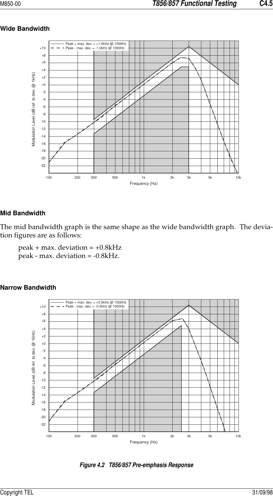
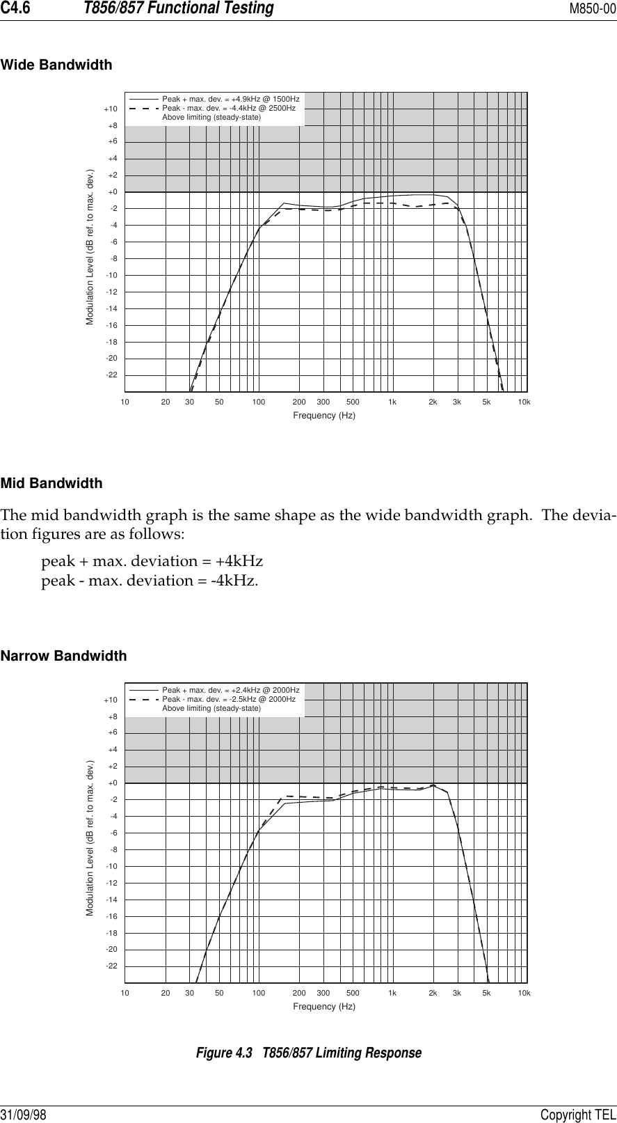
![M850-00T856/857 Functional TestingC4.1Copyright TEL 31/09/984 T856/857 Functional TestingCaution:This equipment contains CMOS devices which are susceptible to dam-age from static charges. Refer to Section 1.2 in Part A for more infor-mation on anti-static procedures when handling these devices.The following test procedures will confirm that the T856/857 has been tuned andadjusted correctly and is fully operational.Note 1:In this and following sections deviation settings are given first for widebandwidth sets, followed by settings in brackets for mid bandwidth sets ( )and narrow bandwidth sets [ ].Note 2:Unless otherwise specified, the term "PGM800Win" used in this and follow-ing sections refers to version 2.00 and later of the software.Refer to Figure 4.4 and Figure 4.5 for the location of the main tuning and adjustmentcontrols, and to Section 3.3 for the test equipment set-up. Refer also to Section 6 wherethe parts lists, grid reference index and diagrams will provide detailed information onidentifying and locating components and test points on the main PCB. The parts listand diagrams for the VCO PCB are in Part E.The following topics are covered in this section.Section Title Page4.1 Current Consumption 4.34.2 Output Power 4.34.3 Output Frequency 4.34.4 Timers 4.34.5 Frequency Response 4.44.6 Audio Level Input Sensitivity 4.7Figure Title Page4.14.24.34.44.5T856/857 Transmit TimersT856/857 Pre-emphasis ResponseT856/857 Limiting ResponseT856 Main Tuning & Adjustment ControlsT857 Main Tuning & Adjustment Controls4.44.54.64.94.11](https://usermanual.wiki/Tait/TEL0033/User-Guide-83794-Page-45.png)
![C4.4T856/857 Functional TestingM850-0031/09/98 Copyright TELFigure 4.1 T856/857 Transmit Timers4.5 Frequency ResponseIf the T856/857 has been correctly adjusted, the pre-emphasis and limiting responsesshould closely match those shown in Figure 4.2 and Figure 4.3 respectively. Note:The limits shown on these graphs should not be exceeded. • Measure the pre-emphasis response as follows: Reduce the line level to give ±1kHz (±0.8kHz) [±0.5kHz] deviation at 1kHz. Sweep the modulation frequency. The response should closely match that shown in Figure 4.2.• Measure the limiting response as follows: Set the line level to give ±3kHz (±2.4kHz) [±1.5kHz] deviation at 1kHz. Increase the line level 20dB and sweep the modulation frequency. The response should closely match that shown in Figure 4.3.Timer Function AdjustmentTransmit Tail Sets the tail time during which the transmitter stays keyed after the exter-nal key source has been removed.0-5 seconds in 100ms stepsTransmit Timeout Sets the maximum continuous trans-mission time. Once the timer has timed out, the transmitter must be keyed again, unless prevented by the transmit lockout timer.0-300 seconds in 10 second stepsTransmit Lockout Sets the period of time that must elapse after a timeout before the trans-mitter can re-transmit. Once the timer has timed out, the transmitter can be keyed again.0-60 seconds in 10 second stepsOnLockout TimeTimeoutTimeOnTail TimeTx-EnableTx-Reg.Tx-EnableTx-Reg.](https://usermanual.wiki/Tait/TEL0033/User-Guide-83794-Page-48.png)
![M850-00T856/857 Functional TestingC4.7Copyright TEL 31/09/984.6 Audio Level Input Sensitivity• Adjust RV210 (line sensitivity) fully clockwise.• Check that the input sensitivities are better than those specified below:Note:A degraded signal to noise ratio can be expected with the compressorselected. The extent of the degradation is dependent on the audio inputlevel.Line Input 600 ohms, ±3kHz (±2.4kHz) [±1.5kHz] deviation at 1kHz: with compressor -50dBm without compressor -30dBmMicrophone Input 600 ohms, ±3kHz (±2.4kHz) [±1.5kHz] deviation at 1kHz: with compressor -75dBm without compressor -55dBmCTCSS Input 1kHz deviation at 150Hz 500mV rms](https://usermanual.wiki/Tait/TEL0033/User-Guide-83794-Page-51.png)

![M850-00T856/857 Fault FindingC5.1Copyright TEL 31/09/985 T856/857 Fault FindingCaution:This equipment contains CMOS devices which are susceptible to dam-age from static charges. Refer to Section 1.2 in Part A for more infor-mation on anti-static procedures when handling these devices.The following test procedures and fault finding flow charts may be used to help locate ahardware problem, however they are by no means a complete fault finding procedure.If you still cannot trace the fault after progressing through them in a logical manner,contact your nearest Tait Dealer or Customer Service Organisation. If necessary, you canget additional technical help from Customer Support, Radio Systems Division, Tait Elec-tronics Ltd, Christchurch, New Zealand (full contact details are on page 2).Note 1:In this and following sections deviation settings are given first for widebandwidth sets, followed by settings in brackets for mid bandwidth sets ( )and narrow bandwidth sets [ ].Note 2:Unless otherwise specified, the term "PGM800Win" used in this and follow-ing sections refers to version 2.00 and later of the software.Refer to Section 6 where the parts lists, grid reference index and diagrams will providedetailed information on identifying and locating components and test points on themain PCB. The parts list and diagrams for the VCO PCB are in Part E.The following topics are covered in this sectionSection Title Page5.1 Visual Checks 5.35.2 Component Checks 5.35.3 Front Panel LED Indicator 5.35.45.4.15.4.2DC ChecksPower RailsVCO Locking5.45.45.45.55.5.15.5.25.5.35.5.4RF ChecksT856 Drive PowerT856 PA Output PowerT857 Output PowerAudio And Modulation5.55.55.55.55.65.6 PGM800Win Generated Errors 5.7](https://usermanual.wiki/Tait/TEL0033/User-Guide-83794-Page-53.png)
![C5.6T856/857 Fault FindingM850-0031/09/98 Copyright TELConnect the exciter output to a power meter and key the exciter.Check that the output power is 1W ±300mW.Note:If the synthesiser is out of lock, the lock detector (synthesiser IC740 andcomparator IC750) will prevent the RF signal from reaching the PA byswitching the supply to the exciter amplifier (Q301, IC300, Q302, Q303).5.5.4 Audio And ModulationRefer to the audio processor fault finding chart (Section 5.7.7).Set up the audio processor as described in Section 3.9.Check that the demodulated RF output has the frequency response referred to inSection 4.5 with at least ±5kHz (±4kHz) [±2.5kHz] deviation available at 1kHzmodulating frequency.If the above result is not achieved, either the two modulators are incorrectly adjusted ora fault condition exists.](https://usermanual.wiki/Tait/TEL0033/User-Guide-83794-Page-58.png)


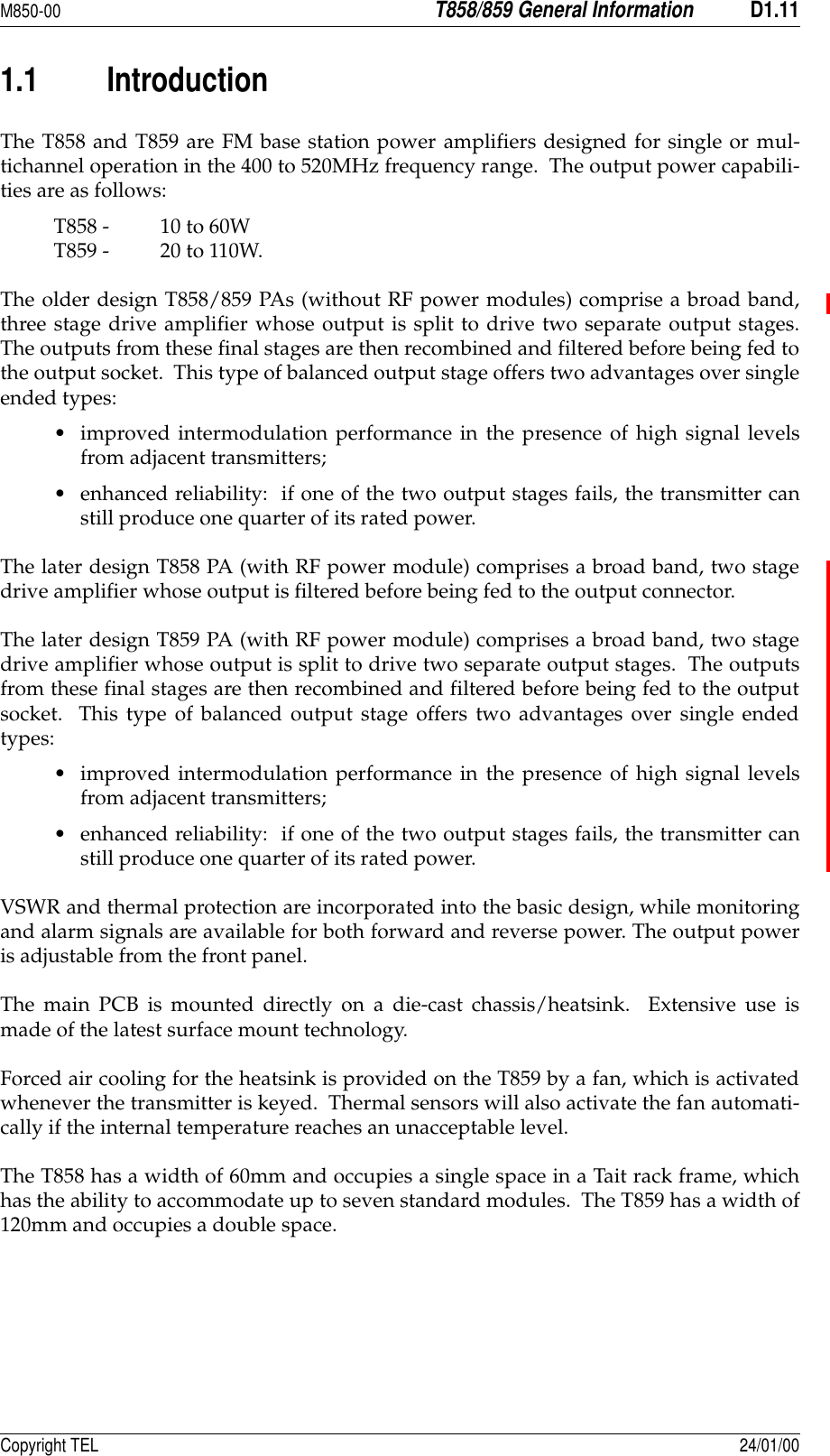
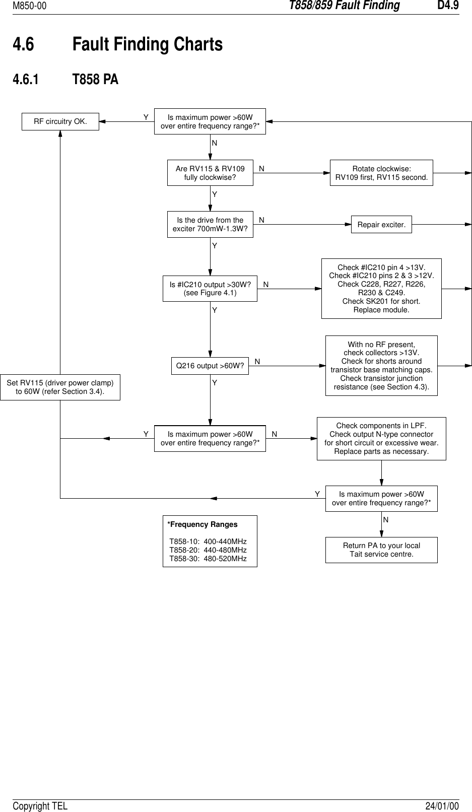
![M850-00T858/859 Circuit OperationD2.1Copyright TEL 24/01/002 T858/859 Circuit OperationThis section provides a basic description of the circuit operation of the T858 and T859power amplifiers.Note:Where the same component has different circuit references in the T858 andT859, in this and following sections the T858 circuit reference is given first,followed by the T859 circuit reference in brackets, e.g. Q137 [Q128].Refer to Section 5 where the parts lists, grid reference index and diagrams will providedetailed information on identifying and locating components. The following topics are covered in this section.Section Title Page2.1 Introduction 2.32.2 RF Circuitry 2.42.32.3.12.3.22.3.32.3.42.3.52.3.6Control CircuitryPower ControlDriver Power LevelThermal ProtectionForward And Reverse Power AlarmsForward And Reverse Power MeteringT859 Fan Control Circuitry2.52.72.72.72.82.82.82.4 Power Supply & Regulator Circuits 2.9Figure Title Page2.12.22.32.42.52.6T858 High Level Block DiagramT859 High Level Block DiagramT858 Control Circuitry Block DiagramT859 Control Circuitry Block DiagramT859 Fan Control Logic DiagramT858/859 Power Supply & Regulator Circuitry Block Diagram2.32.32.52.62.82.9](https://usermanual.wiki/Tait/TEL0033/User-Guide-83794-Page-105.png)

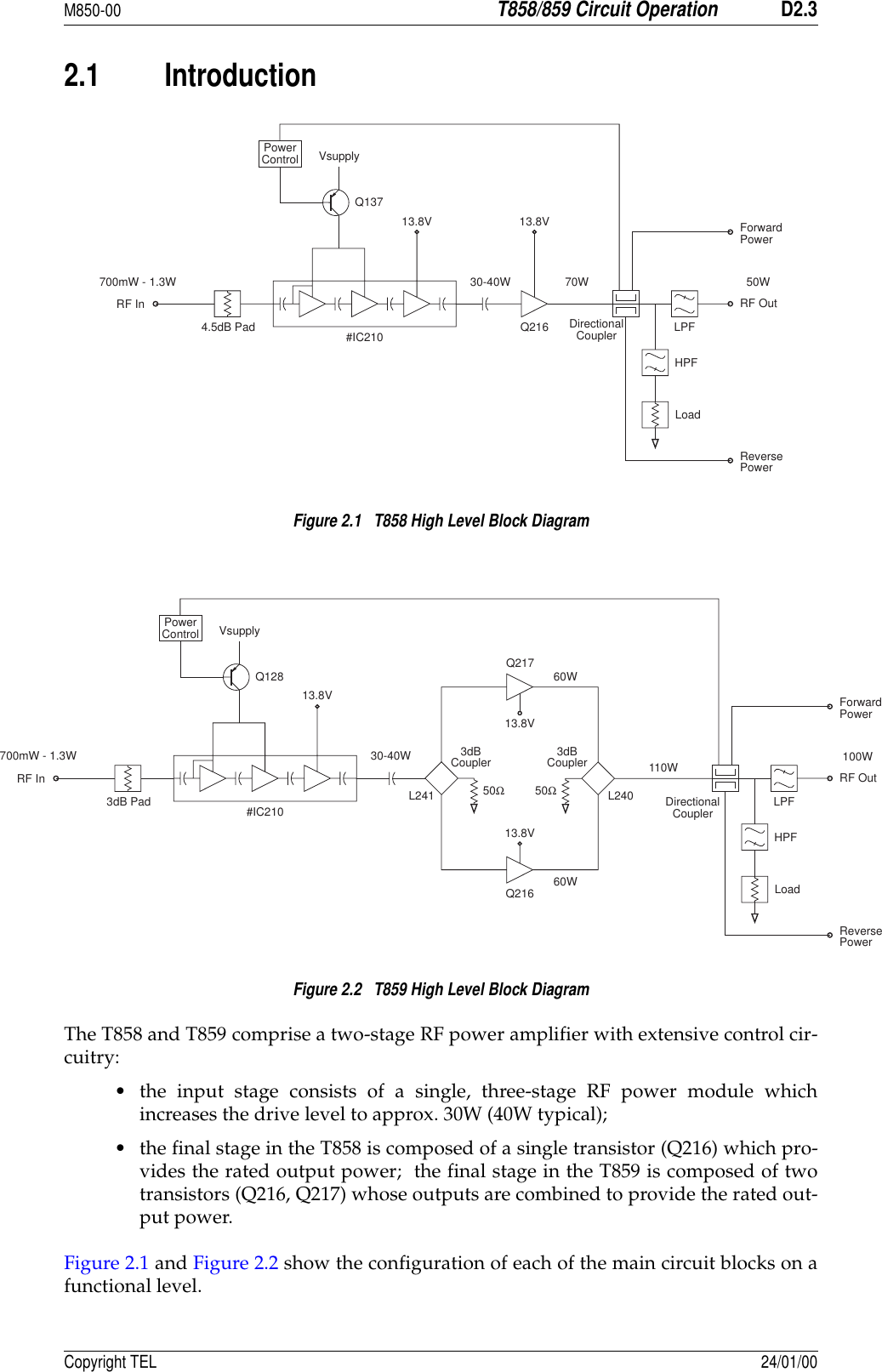
![D2.4T858/859 Circuit OperationM850-0024/01/00 Copyright TEL2.2 RF Circuitry(Refer to Figure 2.1, Figure 2.2 and the RF section circuit diagrams in Section 5.)The driver stage of the T858 consists of a three-stage RF power module (#IC210) whichdelivers 30-40W to the final amplifier (Q216). The output from the final is passed to theantenna socket via the harmonic filter.The driver stage of the T859 consists of a three-stage RF power module (#IC210) whichdelivers 30-40W to the final transistors. The signal is split via a 3dB quadrature hybrid(L241) and used to drive the two final amplifiers (Q216, Q217). The outputs from thesefinal stages are recombined by L240 and passed to the antenna socket via the harmonicfilter.The diplexer presents the final amplifiers with a good load at harmonic frequencies,which helps to achieve the expected harmonic attenuation in the output filter.The directional coupler senses forward and reflected power, which is rectified (D205 &D206) and passed to the control circuitry for metering, alarm and power control pur-poses.Power control is via a series pass transistor (Q137 [Q128]), which controls the supplyvoltage on the first two-stage of #IC210.](https://usermanual.wiki/Tait/TEL0033/User-Guide-83794-Page-108.png)
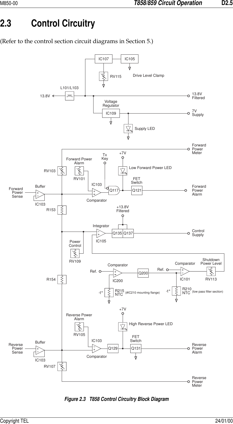
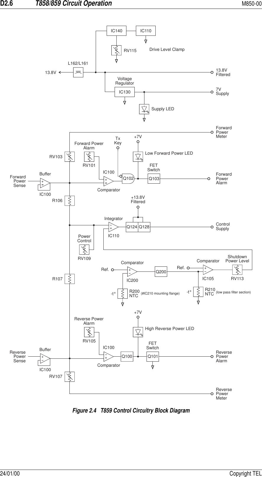
![M850-00T858/859 Circuit OperationD2.7Copyright TEL 24/01/002.3.1 Power ControlThe DC voltages from the directional coupler representing forward and reflected powerare buffered by the two voltage followers, IC103 [IC100] pins 1, 2 & 3 and pins 12, 13 &14. Their outputs are summed at an integrator (IC105 [IC110] pins 1, 2 & 3), whichdrives the series pass control elements (Q135 & Q137 [Q124 & Q128]).Forward and reflected power are summed so that, under high output VSWR, the powercontrol turns the PA down. This is because the control loop adjusts for the same DCvoltage from the directional coupler that would have been present if there were noreflected power.2.3.2 Driver Power LevelThe maximum output power of the T858/859 can be limited by placing a ceiling on thedriver output power level using RV115 (accessible through the side cover). For exam-ple, if RV115 is set for a maximum output power of 50W, the range of adjustment usingRV109 (front panel power adjust) will be 20 to 50W.Caution:The driver power level clamp (RV115) is factory set to give a maximumpower output at room temperature of 60W for the T858 and 110W forthe T859. The unit may be damaged if this level is increased.2.3.3 Thermal ProtectionAt excessively high temperatures, the output power will automatically reduce to a pre-set level (set by RV113), thus preventing the PA from overheating. Ambient temperature within the PA is measured by a thermistor controlled voltagedivider (R168 [R177], R210) which applies a voltage to a comparator with hysteresis(IC101 [IC105] pins 8, 9 & 10). This thermistor is located on the PCB in the low pass fil-ter cavity.Thermal protection is also provided for the RF power module to prevent the moduleitself from overheating. This protection consists of a thermistor controlled voltagedivider (R203, R215 [R200]) which sets a voltage on a comparator with hysteresis (IC200pins 1, 2 & 3). The thermistor is located on the module flange.The output current from all comparators is summed into the power control network viaRV113 so that the power level to which the PA must turn down may be set.](https://usermanual.wiki/Tait/TEL0033/User-Guide-83794-Page-111.png)
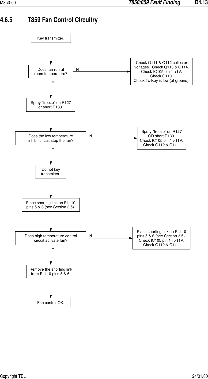
![D2.8T858/859 Circuit OperationM850-0024/01/00 Copyright TEL2.3.4 Forward And Reverse Power AlarmsIf forward power drops below, or reverse power rises above, presettable limits, alarmsmay be triggered.The alarm outputs are open drain configuration and are low under normal conditions(i.e. forward and reverse power levels are normal).IC103 [IC100] pins 5, 6 & 7 and pins 8, 9 & 10 form comparators with thresholdsadjusted via RV101 (forward power) and RV105 (reverse power) respectively. Theinputs are from the forward and reverse power signals from the directional coupler,buffered by IC103 [IC100] pins 1, 2 & 3 and pins 12, 13 & 14. Thus, the power levels atwhich the forward and reverse power alarms are triggered are defined by RV101 andRV105 respectively.2.3.5 Forward And Reverse Power MeteringForward and reverse power signals from the two IC103 [IC100] buffers are available formetering purposes. The output currents are adjustable via RV103 (forward power) andRV107 (reverse power).2.3.6 T859 Fan Control CircuitryFigure 2.5 T859 Fan Control Logic DiagramQ113 Q114 FanRef +High Temp.Sense On PCBComparatorIC105R210High Temp.Sense OnModule FlangeLow Temp.SenseNTCTx KeyInvertQ110 ORQ111,R140, R141Q200NANDQ111, Q112,R142, R143 Fan Driver13.8VFilteredRef +ComparatorIC200R200NTCComparatorRef +IC105R127NTC](https://usermanual.wiki/Tait/TEL0033/User-Guide-83794-Page-112.png)

![M850-00T858/859 Initial AdjustmentD3.1Copyright TEL 24/01/003 T858/859 Initial AdjustmentCaution:This equipment contains CMOS devices which are susceptible to dam-age from static charges. Refer to Section 1.2 in Part A for more infor-mation on anti-static procedures when handling these devices.The following section describes the full adjustment procedure to be carried out beforeoperating the T858/859.Note 1:The T858/859 requires no RF tuning or alignment.Note 2:Where the same component has different circuit references in the T858 andT859, in this and following sections the T858 circuit reference is given first,followed by the T859 circuit reference in brackets, e.g. Q137 [Q128].Refer to Section 5 where the parts lists, grid reference index and diagrams will providedetailed information on identifying and locating components. The following topics are covered in this section.Section Title Page3.1 Test Equipment Required 3.33.2 Shorting Links 3.33.3 Preliminary Checks 3.43.4 Setting The Output Power 3.43.5 High Temperature Shutdown Power Level 3.53.6 Remote Forward Power Meter Calibration 3.53.7 Remote Reverse Power Meter Calibration 3.53.83.8.13.8.2Setting Alarm LevelsForward PowerReverse Power3.63.63.6Figure Title Page3.1 T858/859 Test Equipment Set-up 3.3](https://usermanual.wiki/Tait/TEL0033/User-Guide-83794-Page-115.png)
![M850-00T858/859 Initial AdjustmentD3.3Copyright TEL 24/01/003.1 Test Equipment Required• DC power supply capable of delivering >16A (T858) or >20A (T859) at 13.8V.• Multimeter or DMM (e.g. Fluke 77).• RF power meter (e.g. HP 435 series or Bird Wattmeter). • 150W 30dB attenuator (T858) or 250W 50dB attenuator (T859). • 150W 3dB 50 ohm pad. • 'BNC' to 'N' type adaptors (e.g. Amphenol, Greenpar). • Appropriate trimming tools. Figure 3.1 T858/859 Test Equipment Set-upCaution:Do not connect attenuators or DC blocks between the T857 and T858/859 or the cyclic keying circuitry will not function correctly.3.2 Shorting LinksThere are seven shorting links on PL110 in the control section circuitry, as described inthe table below. Ensure that these links are set as standard before starting and aftercompleting the adjustment procedure.Link Pins Standard Setting Function1-2, 3-4,7-8, 9-10not linked Not used.5-6 not linked Pins 5-6 are provided for simulating high operating temperatures during initial adjustment. Bridging this link shorts out R215 [R200] and R210 (NTCs), thus turning on the thermal protection circuitry. They should not be linked for normal operation.11-1213-14linked Pins 11-12 and 13-14 are provided for fac-tory testing only. The PA will not function correctly if these settings are changed.Exciter PATx KeyRF PowerMeterTx Enable30dbAttenuator(HP 435)](https://usermanual.wiki/Tait/TEL0033/User-Guide-83794-Page-117.png)
![D3.4T858/859 Initial AdjustmentM850-0024/01/00 Copyright TEL3.3 Preliminary ChecksCheck for short circuits between the positive rail and earth.Set up the test equipment as in Figure 3.1.Connect the T858/859 to a 13.8V DC supply.Check that the quiescent current is <50mA.To key the transmitter, earth the key line (pin 13) on the exciter.Check that the power supply is still at 13.8V under load.Check that the regulated power control supply is approximately 7V.Note:The output power and alarm levels should be set with the side cover on. Ifthe cover is removed for other adjustment procedures, make a final check ofthe output power and alarm levels with the side cover on.3.4 Setting The Output PowerCaution:If the high temperature shutdown power level has not yet been set or isunknown, check that the unit does not overheat while setting the out-put power.Note 1:Cables and connectors can easily cause a power loss of several watts if eithertoo long or poorly terminated. Always use the shortest possible leads (orconnectors instead of leads) between the T858/859 and power meter set-up.Note 2:You will need appropriate extension leads if you wish to carry out theadjustment procedures with the T858/859 withdrawn from the rack in thelatched position. Alternatively, disconnect and withdraw the T858/859 andreconnect it behind the rack.Note 3:The actual power used may be limited by regulatory requirements. Connect the exciter output to the PA input via a thru-line wattmeter with a 5Wfull scale reading. Special BNC/N leads will be required.Ensure that PL110 pins 11-12 and 13-14 are linked, and all other pins are notlinked.Connect an RF power meter to the PA output via a 30dB pad.Set RV109 [%RV109] (front panel power control) and RV115 (driver power clamp)fully clockwise.Key on the drive source.](https://usermanual.wiki/Tait/TEL0033/User-Guide-83794-Page-118.png)
![M850-00T858/859 Initial AdjustmentD3.5Copyright TEL 24/01/00Check that the power output exceeds:T858 - 60WT859 - 120W.Note:The side cover access hole for the driver power clamp (RV115) is coveredwith a tamper-proof sticker. The clamp has been factory set to 60W (T858)/110W (T859) maximum output power and should not normally needadjustment. If the output power level is low, check that the high tempera-ture shutdown circuit has not activated by verifying that IC101 [IC105] pin 8is low.Adjust RV115 to reduce the maximum power output to:T858 - 60WT859 - 110W.Adjust RV109 [%RV109] to set the power output to the required level (e.g. 50W forthe T858, 100W for the T859).3.5 High Temperature Shutdown Power LevelSet RV109 [%RV109] (front panel power control) to the required output power.Simulate high operating temperatures by placing a shorting link on PL110 pins 5-6(do not use either of the links from PL110 pins 11-12 or 13-14 to do this).Adjust RV113 (shutdown power level) for an output power of:T858 - 20WT859 - 40W.Remove the shorting link from PL110 pins 5-6 to return the PA to normal opera-tion.3.6 Remote Forward Power Meter CalibrationIf a remote meter is connected, adjust RV103 (forward power meter calibration)for the remote reading to agree with the RF power meter reading.3.7 Remote Reverse Power Meter CalibrationIf a remote meter is connected, connect a 50 ohm 3dB pad (with the output opencircuit) to the PA output.Apply RF drive and Tx-Key.Adjust RV107 (reverse power meter calibration) for a quarter of the forwardpower reading.](https://usermanual.wiki/Tait/TEL0033/User-Guide-83794-Page-119.png)
![D3.6T858/859 Initial AdjustmentM850-0024/01/00 Copyright TEL3.8 Setting Alarm LevelsNote:If forward and reverse power metering is being used, set up their calibration(Section 3.6 and Section 3.7) before setting the alarm levels.3.8.1 Forward PowerPower up the T858/859 and adjust RV109 [%RV109] (front panel power control)so that the output power is at the alarm level required (e.g. 40W if the T858 nor-mally operates at 50W).Adjust RV101 (forward power alarm set) so that the forward power alarm LEDlights.Check the alarm level setting by adjusting the power up and down and observingthe alarm LED. A few watts hysteresis can be expected.Readjust RV109 [%RV109] for the normal operating level.Note:Remote indication is available at pin 3 of D-range 1.3.8.2 Reverse PowerPower up the T858/859 and adjust RV109 [%RV109] (front panel power control)for the normal operating power level.Place a known mismatch of the required value (e.g. 3:1 VSWR) and adjust RV105(reverse power alarm set) so that the reverse power alarm LED lights.Example:A VSWR of 3:1 can be simulated by connecting an unterminated 3dB pad(50W) to the PA output. This will result in a return loss of 6dB.Note:Remote indication is available at pin 4 of D-range 1.](https://usermanual.wiki/Tait/TEL0033/User-Guide-83794-Page-120.png)
![M850-00T858/859 Fault FindingD4.1Copyright TEL 24/01/004 T858/859 Fault FindingCaution:This equipment contains CMOS devices which are susceptible to dam-age from static charges. Refer to Section 1.2 in Part A for more infor-mation on anti-static procedures when handling these devices.The following test procedures and fault finding flow charts may be used to help locate ahardware problem, however they are by no means a complete fault finding procedure.If you still cannot trace the fault after progressing through them in a logical manner,contact your nearest Tait Dealer or Customer Service Organisation. If necessary, youcan get additional technical help from Customer Support, Radio Systems Division, TaitElectronics Ltd, Christchurch, New Zealand (full contact details are on page 2).Note:Where the same component has different circuit references in the T858 andT859, in this and following sections the T858 circuit reference is given first,followed by the T859 circuit reference in brackets, e.g. Q137 [Q128].Refer to Section 5 where the parts lists, grid reference index and diagrams will providedetailed information on identifying and locating components.The following topics are covered in this section.Section Title Page4.1 Visual Checks 4.34.2 Shorting Links 4.34.3 Component Checks 4.34.4 DC Checks 4.44.54.5.14.5.2RF ChecksT858T8594.44.44.54.64.6.14.6.24.6.34.6.44.6.5Fault Finding ChartsT858 PAT859 PAT858 Power ControlT859 Power ControlT859 Fan Control Circuitry4.94.94.104.114.124.134.7 Replacing RF Power Transistors 4.144.8 Replacing RF Power Modules 4.164.9 Removing The PCB From The Heatsink 4.17](https://usermanual.wiki/Tait/TEL0033/User-Guide-83794-Page-121.png)
![M850-00T858/859 Fault FindingD4.3Copyright TEL 24/01/004.1 Visual ChecksRemove the side cover from the T858/859 and inspect the PCB for damaged orbroken components, paying particular attention to the surface mounted devices(SMDs). Also check for defective solder joints.Refer to Section 4.7, Section 4.8, Section 4.9 and Section 3 of Part A for more detailson repair and replacement of components.4.2 Shorting LinksThere are seven shorting links on PL110 in the control section circuitry, as described inthe table below. Ensure that these links are set as standard before starting and aftercompleting the adjustment procedure.4.3 Component ChecksIf you suspect a transistor is faulty, you can assess its performance by measuring the for-ward and reverse resistance of the junctions. Unless the device is completely desol-dered, first make sure that the transistor is not shunted by some circuit resistance (e.g. abase choke). Use a good quality EVM (e.g. Fluke 75) for taking the measurements (or a20k ohm/V or better multimeter, using only the medium or low resistance ranges).Caution:Before operating the PA, replace any RF base chokes removed whilemaking measurements.The collector current drawn by multi-junction transistors is a further guide to their per-formance.Link Pins Standard Setting Function1-2, 3-4,7-8, 9-10not linked Not used.5-6 not linked Pins 5-6 are provided for simulating high operating temperatures during initial adjustment. Bridging this link shorts out R215 [R200] and R210 (NTCs), thus turning on the thermal protection circuitry. They should not be linked for normal operation.11-1213-14linked Pins 11-12 and 13-14 are provided for fac-tory testing only. The PA will not function correctly if these settings are changed.](https://usermanual.wiki/Tait/TEL0033/User-Guide-83794-Page-123.png)

![D4.18T858/859 Fault FindingM850-0024/01/00 Copyright TELCaution:Do not operate the PA with the PCB detached as the heatsink is usedfor earthing and heat dissipation.To replace the PCB, reverse the order of removal, taking care that the wiring is cor-rectly positioned and not 'pinched'.Make sure that the heatsink compound has stayed clean, and that the insulatingpad for Q137 [Q128] is not damaged.If you have difficulty refitting the LEDs, try pushing the body of the LED backinto the grommet with a thin screwdriver or spike.](https://usermanual.wiki/Tait/TEL0033/User-Guide-83794-Page-138.png)