Tait TEL0033 Base Station Transmitter User Manual 8c500 bk
Tait Limited Base Station Transmitter 8c500 bk
Tait >
Cct Description Part List Manual

M850-00
T856/857 General Information
C1.1
Copyright TEL 31/09/98
1 T856/857 General Information
This section provides a brief description of the T856 transmitter and T857 exciter, along
with detailed specifications and a list of types available.
The following topics are covered in this section.
Section Title Page
1.1 Introduction 1.7
1.2
1.2.1
1.2.2
1.2.3
1.2.4
1.2.4.1
1.2.4.2
1.2.4.3
1.2.5
1.2.6
1.2.6.1
1.2.6.2
1.2.6.3
Specifications
Introduction
General
RF Section
Audio Processor
Inputs
Modulation Characteristics
CTCSS
Microcontroller
Test Standards
European Telecommunication Standard
DTI CEPT Recommendation T/R-24-01
Telecommunications Industry Association
1.8
1.8
1.8
1.9
1.10
1.10
1.11
1.11
1.11
1.12
1.12
1.12
1.12
1.3 Product Codes 1.13
1.4 T856 Standard Product Range 1.14
1.5 T857 Standard Product Range 1.15
Figure Title Page
1.1 T856 Main Circuit Block Identification 1.4
1.2 T856 Front Panel Controls 1.4
1.3 T857 Main Circuit Block Identification 1.6
1.4 T857 Front Panel Controls 1.6

C1.2
T856/857 General Information
M850-00
31/09/98 Copyright TEL

M850-00
T856/857 General Information
C1.3
Copyright TEL 31/09/98
replace A4 pages C1.3/C1.4 with A3 pages C1.3/C1.4

C1.4
T856/857 General Information
M850-00
31/09/98 Copyright TEL
replace A4 pages C1.3/C1.4 with A3 pages C1.3/C1.4

M850-00
T856/857 General Information
C1.5
Copyright TEL 31/09/98
replace A4 pages C1.5/C1.6 with A3 pages C1.5/C1.6

C1.6
T856/857 General Information
M850-00
31/09/98 Copyright TEL
replace A4 pages C1.5/C1.6 with A3 pages C1.5/C1.6

M850-00
T856/857 General Information
C1.7
Copyright TEL 31/09/98
1.1 Introduction
The T856 is a synthesised, microprocessor controlled FM base station transmitter
designed for single or multichannel operation in the 400 to 520MHz frequency range1
with a standard power output of 25W. The RF section of the transmitter comprises a fre-
quency synthesiser which provides 100mW of frequency modulated RF drive to a two
stage, wide band output driver followed by a 25W power amplifier. A thermal shut-
down feature is provided in the T856 in case operating temperatures exceed acceptable
levels.
The T857 is a synthesised, microprocessor controlled FM base station exciter designed
for single or multichannel operation in the 400 to 520MHz frequency range1. With a
standard power output of only 1W, the exciter is designed for use with the T858 50W or
T859 100W power amplifiers. The RF section of the exciter comprises a frequency syn-
thesiser which provides 100mW of frequency modulated RF drive to a two stage, wide
band output amplifier.
A wide selection of audio characteristics may be obtained from the audio processor.
Optional circuit blocks are an audio compressor and a pre-emphasis stage. They can be
bypassed or linked to one or both audio inputs, and then back into the remaining audio
circuitry in almost any combination. All audio processor options are link selectable.
The synthesiser frequency is programmed via the serial communications port. Eight
channel select lines are accessible via an optional D-range connector (D-range 2 -
T800-03-0000) at the rear of the set.
All components except those of the VCO are mounted on a single PCB. This is secured
to a die-cast chassis which is divided into compartments to individually shield each sec-
tion of circuitry. Access to both sides of the main circuit board is obtained by removing
each of the chassis lids. There is provision within the chassis to mount small option
PCBs.
The front panel controls include line sensitivity, microphone socket and carrier switch.
This switch turns on the carrier (unmodulated) as an aid to servicing.
The T856 and T857 are both 60mm wide and each occupies a single space in a Tait rack
frame, which has the ability to accommodate up to seven standard modules.
1. Although capable of operating over the 400-520MHz frequency range, the T856 and
T857 have an 8MHz switching range (see Section 1.2.3 and Section 3.1).
C1.8
T856/857 General Information
M850-00
31/01/99 Copyright TEL
1.2 Specifications
1.2.1 Introduction
The performance figures given are minimum figures, unless otherwise indicated, for
equipment tuned with the maximum switching range and operating at standard room
temperature (+22°C to +28°C) and standard test voltage (13.8V DC).
Where applicable, the test methods used to obtain the following performance figures are
those described in the EIA and ETS specifications. However, there are several parame-
ters for which performance according to the CEPT specification is given. Refer to Sec-
tion 1.2.6 for details of test standards.
Details of test methods and the conditions which apply for Type Approval testing in all
countries can be obtained from Tait Electronics Ltd.
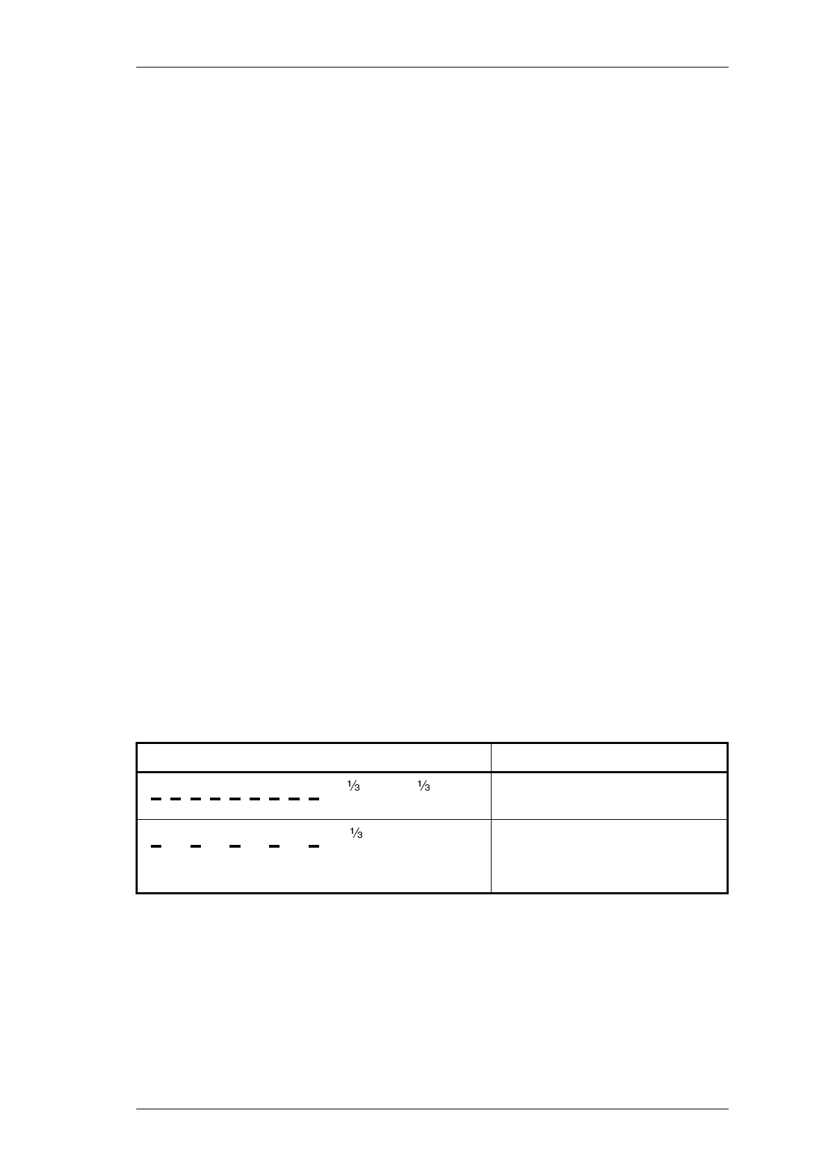
The terms "wide bandwidth", "mid bandwidth" and "narrow bandwidth" used in this
and following sections are defined in the following table.
1.2.2 General
Number Of Channels .. 128 (standard)1
Supply Voltage:
Operating Voltage .. 10.8 to 16V DC
Standard Test Voltage .. 13.8V DC
Polarity .. negative earth only
Polarity Protection .. diode
Supply Current:
Transmit - T856 .. 5.5A (typical)
- T857 .. 750mA
Standby - T856 .. 165mA (typical)
- T857 .. 150mA (typical)
Operating Temperature Range .. -20°C to +60°C
Channel Spacing Modulation
100% Deviation Receiver
IF Bandwidth
Wide Bandwidth 25kHz ±5.0kHz 15.0kHz
Mid Bandwidth 20kHz ±4.0kHz 12.0kHz
Narrow Bandwidth 12.5kHz ±2.5kHz 7.5kHz
1. Additional channels may be factory programmed. Contact your nearest Tait Dealer or
Customer Service Organisation.

M850-00
T856/857 General Information
C1.9
Copyright TEL 31/09/98
Dimensions:
Height .. 183mm
Width .. 60mm
Length .. 320mm
Weight .. 2.1kg
Time-Out Timer (optional) .. 0 to 5 minutes adjustable in 10 second
steps
Tail Timer .. 0 to 5 seconds adjustable in 100ms
steps
Transmit Key Time .. <30ms
Transmit Lockout Timer .. 0 to 1 minute adjustable in 10 second
steps
1.2.3 RF Section
Frequency Range .. 400-520MHz (refer to Section 1.4 and
Section 1.5)
Modulation Type .. FM
Frequency Increment .. 5 or 6.25kHz
Switching Range .. 8MHz (i.e. ±4MHz from the centre
frequency)
Load Impedance .. 50 ohms
Frequency Stability .. ±1ppm, -20°C to +60°C
(see also Section 1.4 and Section 1.5)
Adjacent Channel Power (full deviation):
Wide Bandwidth (WB) .. -75dBc
(±25kHz/15kHz B/W)
Mid Bandwidth (MB) .. -70dBc
(±20kHz/12kHz B/W)
Narrow Bandwidth (NB) .. -65dBc
(±12.5kHz/7.5kHz B/W)
(Transmitter switching must comply with ETS 300 113)
Transmitter Side Band Noise:
(no modulation, 15kHz bandwidth)
At ±25kHz .. -95dBc
At ±1MHz .. -105dBc

C1.10
T856/857 General Information
M850-00
31/09/98 Copyright TEL
Intermodulation .. -40dBc with interfering signal of
-30dBc
.. -70dBc with 25dB isolation
& interfering signal of -30dBc
(PA with output isolator)
T856 Mismatch Capability:
Ruggedness .. refer to your nearest Tait Dealer or
Customer Service Organisation
Stability .. 3:1 VSWR (all phase angles)
Radiated Spurious Emissions:
Transmit .. -36dBm to 1GHz
-30dBm 1GHz to 4GHz
Standby .. -57dBm to 1GHz
-47dBm 1GHz to 4GHz
Conducted Spurious Emissions: (T856 Only)
Transmit .. -36dBm to 1GHz
-30dBm 1GHz to 4GHz
Standby .. -57dBm to 1GHz
-47dBm 1GHz to 4GHz
Power Output:
T856 - Rated Power .. 25W (see Duty Cycle)
- Range Of Adjustment .. 5-25W
T857 .. 1W ±300mW
Duty Cycle (T856 Only) .. 100% @ 25W at +25°C
.. 25% @ 25W at +60°C
.. 100% @ 10W at +40°C
1.2.4 Audio Processor
1.2.4.1 Inputs
Inputs Available .. line, microphone and CTCSS
Line Input:
Impedance .. 600 ohms (balanced)
Sensitivity (60% modulation @ 1kHz)-
With Compressor .. -50dBm
Without Compressor .. -30dBm
Microphone Input:
Impedance .. 600 ohms
Sensitivity (60% modulation @ 1kHz)-
With Compressor .. -70dBm
Without Compressor .. -50dBm

M850-00
T856/857 General Information
C1.11
Copyright TEL 31/01/99
1.2.4.2 Modulation Characteristics
Frequency Response .. flat or pre-emphasised (optional)
(below limiting)
Line And Microphone Inputs:
Pre-emphasised Response-
Bandwidth .. 300Hz to 3kHz (WB & MB)
.. 300Hz to 2.55kHz (NB)
Below Limiting .. within +1, -3dB of a 6dB/octave
pre-emphasis characteristic
Flat Response .. within +1, -2dB of output at 1kHz
Above Limiting Response .. within +1, -2dB of a flat response
(ref. 1kHz)
Distortion .. 2%
Hum And Noise:
Wide Bandwidth .. -55dB (300Hz to 3kHz [EIA]) typical
Mid Bandwidth .. -54dB (CEPT)
Narrow Bandwidth .. -50dB (CEPT)
Compressor (optional):
Attack Time .. 10ms
Decay Time .. 800ms
Range .. 50dB
1.2.4.3 CTCSS
Standard Tones .. all 37 EIA group A, B and C tones
plus 13 commonly used tones
Frequency Error .. 0.08% max.
(from EIA tones)
Generated Tone Distortion .. 1.2% max.
Generated Tone Flatness .. flat across 67 to 250.3Hz to within 1dB
Modulation Level .. adjustable
Modulated Distortion .. <5%
1.2.5 Microcontroller
Auxiliary Ports:
Open Drain Type .. capable of sinking 2.25mA via 2k2Ω
Vds max. .. 5V

C1.12
T856/857 General Information
M850-00
31/09/98 Copyright TEL
1.2.6 Test Standards
Where applicable, this equipment is tested in accordance with the following standards.
1.2.6.1 European Telecommunication Standard
ETS 300 086 January 1991
Radio equipment and systems; land mobile service; technical characteristics and test
conditions for radio equipment with an internal or external RF connector intended pri-
marily for analogue speech.
ETS 300 113 March 1996
Radio equipment and systems; land mobile service; technical characteristics and test
conditions for radio equipment intended for the transmission of data (and speech) and
having an antenna connector.
ETS 300 219 October 1993
Radio equipment and systems; land mobile service; technical characteristics and test
conditions for radio equipment transmitting signals to initiate a specific response in the
receiver.
ETS 300 279 February 1996
Radio equipment and systems; electromagnetic compatibility (EMC) standard for pri-
vate land mobile radio (PMR) and ancillary equipment (speech and/or non-speech).
1.2.6.2 DTI CEPT Recommendation T/R-24-01
Annex I: 1988
Technical characteristics and test conditions for radio equipment in the land mobile
service intended primarily for analogue speech.
Annex II: 1988
Technical characteristics of radio equipment in the land mobile service with regard to
quality and stability of transmission.
1.2.6.3 Telecommunications Industry Association
ANSI/TIA/EIA-603-1992
Land mobile FM or PM communications equipment measurement and performance
standards.

M850-00
T856/857 General Information
C1.13
Copyright TEL 31/09/98
1.3 Product Codes
The three groups of digits in the T850 Series II product code provide information about
the model, type and options fitted, according to the conventions described below.
The following explanation of T850 Series II product codes is not intended to suggest that
any combination of features is necessarily available in any one product. Consult your
nearest Tait Dealer or Customer Service Organisation for more information regarding
the availability of specific models, types and options.
Model
The Model group indicates the basic function of the product, as follows:
T85X-XX-XXXX T855 receiver
T856 25W transmitter
T857 exciter
T858 50W power amplifier
T859 100W power amplifier
Type
The Type group uses two digits to indicate the basic RF configuration of the product.
The first digit in the Type group designates the frequency range:
T85X-XX-XXXX ’1’ for 400-440MHz
’2’ for 440-480MHz
’3’ for 480-520MHz
The second digit in the Type group indicates the channel spacing:
T85X-XX-XXXX ’0’ for wide bandwidth (25kHz)
’3’ for mid bandwidth (20kHz)
’5’ for narrow bandwidth (12.5kHz)
Options
T85X-XX-XXXX The Options group uses four digits and/or letters to indicate
any options that may be fitted to the product. This includes
standard options and special options for specific customers.
’0000’ indicates a standard Tait product with no options fitted.
The large number of options precludes listing them here.

C1.14
T856/857 General Information
M850-00
31/01/99 Copyright TEL
1.4 T856 Standard Product Range
The following table lists the range of standard T856 types (i.e. no options fitted) availa-
ble at the time this manual was published. Consult your nearest Tait Dealer or Cus-
tomer Service Organisation for more information.
Caution:
T856-1X-XXXX Product Types
The 406 to 406.1MHz frequency range is reserved worldwide for use by
Distress Beacons. Do not program transmitters to operate in this fre-
quency range.
You can identify the transmitter type by checking the product code printed on a label on
the rear of the chassis (Figure 1.1 in Part A shows typical labels). You can further verify
the transmitter type by checking the placement of an SMD resistor in the table that is
screen printed onto the PCB (refer to Section 6.1 for more details).
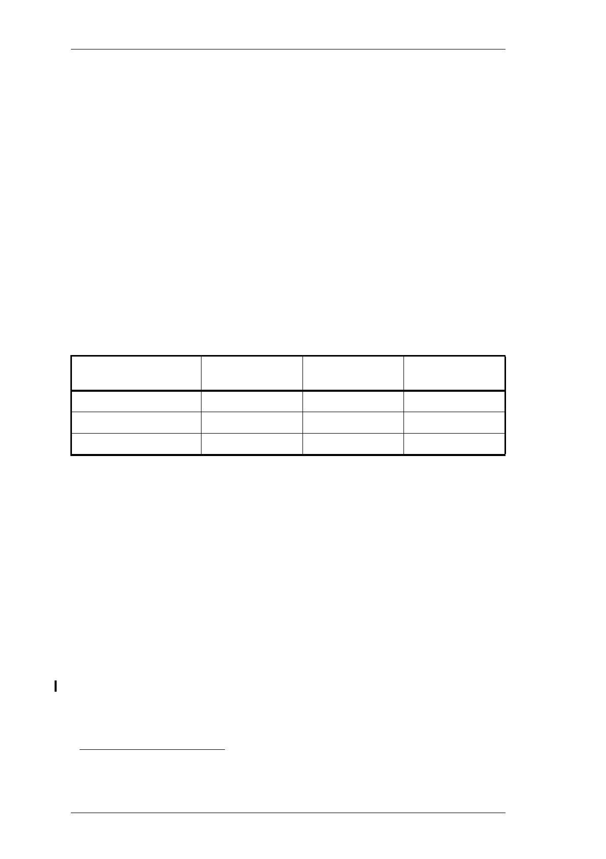
Frequency Range (MHz) 400-440
Deviation (kHz) 2.5 2.5 4 5
TCXO ±1ppm -20°C to +60°C ••••
Transmitter Type: T856- 16-0000a
a. United States market only.
15-0000 13-0000 10-0000
Frequency Range (MHz) 440-480
Deviation (kHz) 2.5 2.5 4 5
TCXO ±1ppm -20°C to +60°C ••••
Transmitter Type: T856- 26-0000a25-0000 23-0000 20-0000
Frequency Range (MHz) 480-512 480-520
Deviation 2.5 2.5 5
TXCO ±1ppm -20° to +60°C •••
Transmitter Type: T856- 36-0000a35-0000 30-0000
M850-00
T856/857 General Information
C1.15
Copyright TEL 31/01/99
1.5 T857 Standard Product Range
The following table lists the range of standard T857 types (i.e. no options fitted and
cyclic keying disabled) available at the time this manual was published. Consult your
nearest Tait Dealer or Customer Service Organisation for more information.
Caution:
T857-1X-XXXX Product Types
The 406 to 406.1MHz frequency range is reserved worldwide for use by
Distress Beacons. Do not program exciters to operate in this frequency
range.
You can identify the exciter type by checking the product code printed on a label on the
rear of the chassis (Figure 1.1 in Part A shows typical labels). You can further verify the
exciter type by checking the placement of an SMD resistor in the table that is screen
printed onto the PCB (refer to Section 6.1 for more details).
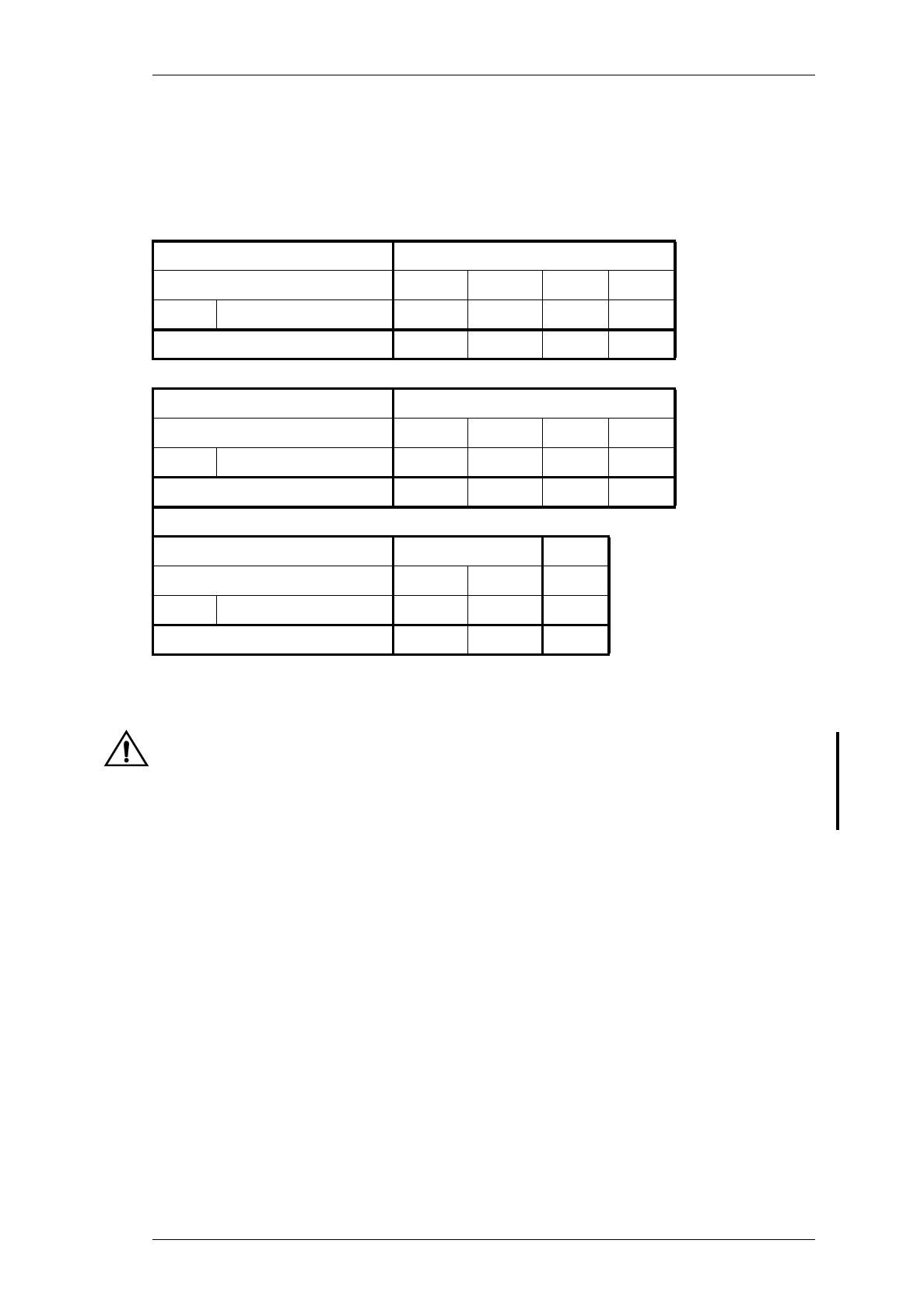
Frequency Range (MHz) 400-440
Deviation (kHz) 2.5 2.5 4 5
TCXO ±1ppm -20°C to +60°C ••••
Exciter Type: T857- 16-0000a
a. United States market only.
15-0000 13-0000 10-0000
Frequency Range (MHz) 440-480
Deviation (kHz) 2.5 2.5 4 5
TCXO ±1ppm -20°C to +60°C ••••
Exciter Type: T857- 26-0000a25-0000 23-0000 20-0000
Frequency Range (MHz) 480-512 480-520
Deviation 2.5 2.5 5
TXCO ±1ppm -20° to +60°C •••
Exciter Type: T857- 36-0000a35-0000 30-0000

C1.16
T856/857 General Information
M850-00
31/09/98 Copyright TEL

M850-00
T856/857 Circuit Operation
C2.1
Copyright TEL 31/09/98
2 T856/857 Circuit Operation
This section provides a basic description of the circuit operation of the T856 transmitter
and T857 exciter.
Note:
Unless otherwise specified, the term "PGM800Win" used in this and follow-
ing sections refers to version 2.00 and later of the software.
Refer to Section 6 where the parts lists, grid reference index and diagrams will provide
detailed information on identifying and locating components and test points on the
main PCB. The parts list and diagrams for the VCO PCB are in Part E.
The following topics are covered in this section.
Section Title Page
2.1 Introduction 2.3
2.2 Microcontroller 2.4
2.3
2.3.1
Synthesised Local Oscillator
Two Point Modulation
2.5
2.6
2.4
2.4.1
VCO
VCO Supply
2.7
2.7
2.5
2.5.1
2.5.2
2.5.3
2.5.4
2.5.5
Audio Processor
General
Audio Inputs
Keying Inputs
Compressor (Automatic Level Control (ALC))
Outputs To Modulators
2.8
2.8
2.8
2.9
2.9
2.9
2.6 Power Supply & Regulator Circuits 2.10
2.7 Transmit Timers 2.11
2.8 T856 Drive Amplifier & PA 2.12
2.9 T857 Exciter Drive Amplifier 2.13

C2.2
T856/857 Circuit Operation
M850-00
31/09/98 Copyright TEL
Figure Title Page
2.1
2.2
2.3
2.4
2.5
2.6
2.7
2.8
T856 High Level Block Diagram
T857 High Level Block Diagram
T856/857 Microcontroller Block Diagram
T856/857 Synthesiser Block Diagram
T856/857 Two Point Modulation
T856/857 Audio Processor Block Diagram
T856/857 Power Supply & Regulators Block Diagram
T856/857 Transmit Timers
2.3
2.3
2.4
2.5
2.6
2.8
2.10
2.11
M850-00
T856/857 Circuit Operation
C2.3
Copyright TEL 31/09/98
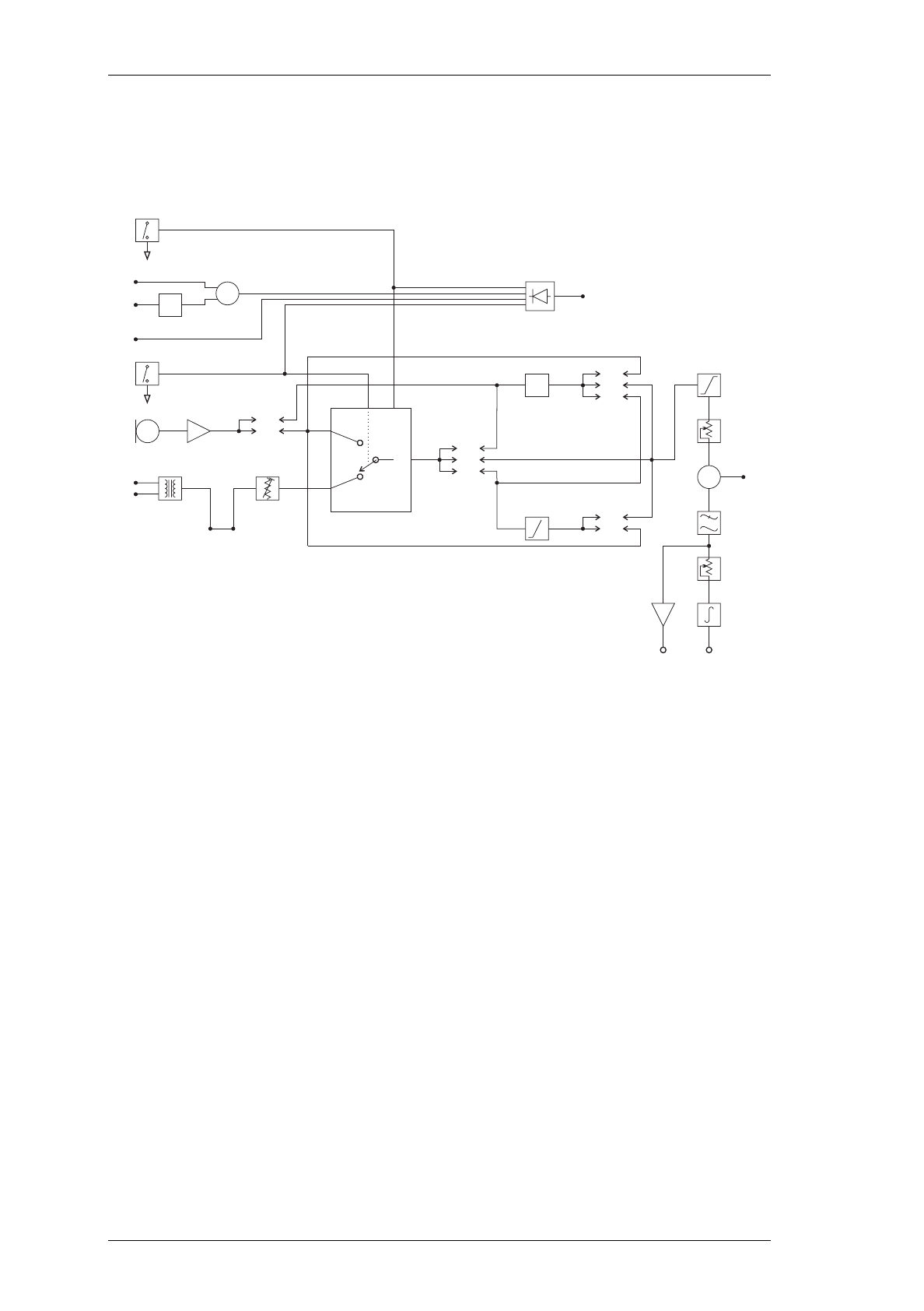
2.1 Introduction
The individual circuit blocks which make up the T856 and T857 are:
• synthesiser
•VCO
• audio processor
• drive amplifier
• power amplifier (T856 only)
• voltage regulators.
Each of these circuit blocks is set in its own shielded compartment, formed as an inte-
gral part of the main chassis.
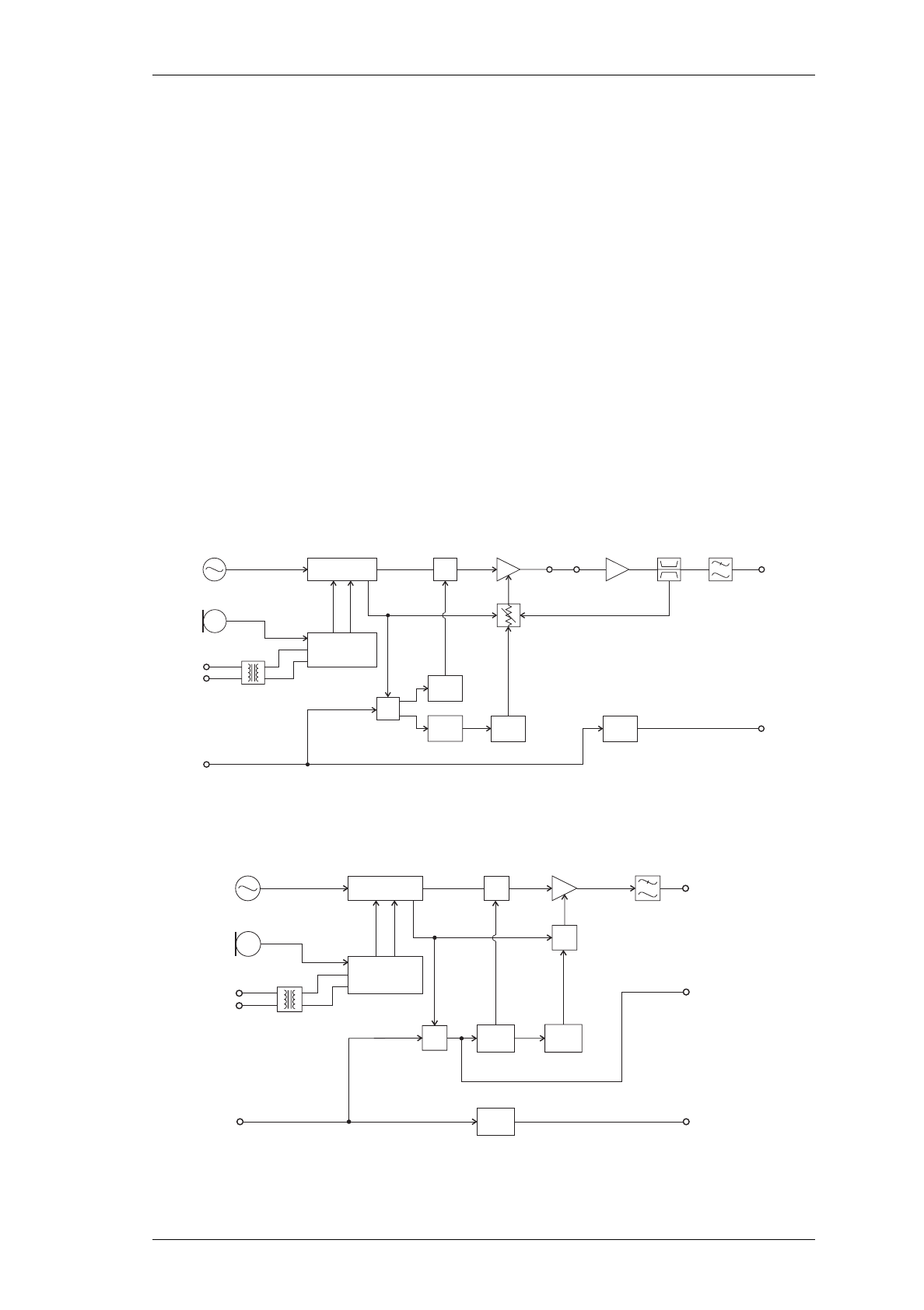
The configuration of the circuit blocks may be seen on a functional level in Figure 2.1
and Figure 2.2. Refer to the circuit diagrams in Section 6.2 (T856) or 6.3 (T857) for more
detail.
Figure 2.1 T856 High Level Block Diagram
Figure 2.2 T857 High Level Block Diagram
Ramp
Gen.
Time
Delay
Time
Delay
Time
Delay
Audio
Processor
Synthesiser +22dBm
Reference
Oscillator
12.8MHz
Microphone
Line
Transformer
Lock
Detect
PIN
Switch
Power
Control
Drive
Amp. PA
VCO
Gate
Directional
Coupler Low Pass
Filter
Exciter
Output
(+30dBm to
+33dBm) Transmitter
Output
(25W)
Tx Reg
&
Audio
Processor
Synthesiser +22dBm
Reference
Oscillator
12.8MHz
Microphone
Line
Transformer
Lock
Detect
PIN
Switch
Switching
Control
Drive
Amp.
Gate
Exciter
Output
(+28dBm to
+31dBm)
&Ramp
Gen.
Tx Reg VCO
Time
Delay
Time
Delay
Low Pass
Filter
PA Control Signal
(via exciter RF coax)

C2.4
T856/857 Circuit Operation
M850-00
31/01/99 Copyright TEL
2.2 Microcontroller
(Refer to the microcontroller circuit diagram (sheet 8) in Section 6.2 or 6.3.)
Figure 2.3 T856/857 Microcontroller Block Diagram
Overall system control of the T856/857 is accomplished by the use of a member of the
80C51 family of microcontrollers (IC810). It runs from internal ROM and RAM, thus
leaving all four ports free for input/output functions.
Non-volatile data storage is achieved by serial communication with a 16kBit EEPROM
(IC820). This serial bus is also used by the microcontroller to program the synthesiser
(IC740) and deviation control EPOTS (IC220).
The main tasks of the microcontroller are as follows:
• program the synthesiser and EPOT;
• interface with the PGM800Win programming software at 9600 baud via the
serial communication lines on D-range 1 (PL100) & D-range 2;
• monitor channel change inputs from D-range 2;
• generate timing waveforms for CTCSS encoding;
• coordinate and implement timing control of the exciter/transmitter.
5V Reset
5V Digital
Regulator Watchdog
Reset
Channel
Select
Port
Auxiliary
Output
Port
Microcontroller
12.8MHz
Clock
Microcontroller Cavity
CTCSS Tone
External
Serial
Port
EEPROM Synthesiser
Dual Digital
Potentiometer
CTCSS
Encoder
Converter

M850-00
T856/857 Circuit Operation
C2.5
Copyright TEL 31/09/98
2.3 Synthesised Local Oscillator
(Refer to the synthesiser circuit diagram (sheet 7) in Section 6.2 or 6.3 and the VCO cir-
cuit diagram in Part E.)
Figure 2.4 T856/857 Synthesiser Block Diagram
The synthesiser (IC740) employs a phase-locked loop (PLL) to lock a voltage controlled
oscillator (VCO) to a given reference frequency. The synthesiser receives the divider
information from the control microprocessor via a 3 wire serial bus (clock, data, enable).
When the data has been latched in, the synthesiser processes the incoming signals from
the VCO buffer (fin) and the phase modulator (fref).
A reference oscillator at 12.8MHz (=IC700) is buffered (IC710 pins 3 & 4) and divided
down to 200kHz (IC730). This 200kHz square wave is then summed with the modulat-
ing audio and passed to an integrator (IC720 pins 9 & 8, Q710, Q720). This produces a
ramping waveform which is centred around a DC level determined by the incoming
audio. IC720 pins 5 & 6 perform as a comparator, ultimately producing a phase-modu-
lated 200kHz square wave. This is followed by another phase shifting stage (IC720 pins
3 & 4, Q730, Q740), before being divided down to 6.25kHz or 5kHz within the synthe-
siser IC (IC740).
A buffered output of the VCO (Q795) is divided with a prescaler and programmable
divider which is incorporated into the synthesiser chip (IC740). This signal is compared
with the phase modulated reference signal at the phase detector (also part of the synthe-
siser chip). The phase detector outputs drive a balanced charge pump circuit (Q760,
Q770, Q775, Q780, Q785) and active loop filter (IC750 pins 5, 6 & 7, Q790) which pro-
duces a DC voltage between 0V and 20V to tune the VCO. This VCO control line is fur-
ther filtered to attenuate noise and other spurious signals. Note that the VCO frequency
increases with increasing control voltage.
If the synthesiser loop loses lock, a pulsed signal appears at LD (pin 2) of IC740. This
signal is filtered and buffered by IC750 pins 1, 2 & 3, producing the Lock-Detect signal
used to shut off the power supply to the drive amplifier. IC750 pin 1 is at 20V when the
synthesiser is out of lock.
/R
Reference
Divider
12.8MHz
Reference
Oscillator Fixed
Divider
/64
Phase
Modulator
Ref
Mod
Phase
Detector Charge
Pump Loop
Filter
FREQUENCY SYNTHESISER IC
Serial
Bus
Clk
Data
En Controller
/N
Programmable
Divider
64/65
Prescaler
VCO PCB
VCO
Modulation
VCO Buffer Output
Buffer
+22dB
m
L.O.
Divider Buffer
f
ref
f
in
Σ
C2.6
T856/857 Circuit Operation
M850-00
31/09/98 Copyright TEL
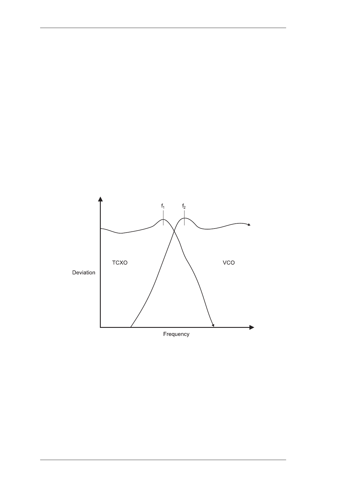
2.3.1 Two Point Modulation
Frequency modulation occurs by modulating both the VCO input and the synthesiser
reference input. This process is called two point modulation and ensures a flat modula-
tion response from 67Hz to 3kHz (2.55kHz for narrow bandwidth).
The PLL has a fast response time, allowing a Tx key-up time of <30ms. Because of this
fast response time the PLL sees lower modulation frequencies superimposed on the
VCO as an error and corrects for it, resulting in no modulation on the carrier. At modu-
lation frequencies greater than 300Hz the loop cannot correct fast enough and modula-
tion is seen on the carrier. The response of the loop to VCO modulation is shown by f2
in Figure 2.5 below.
To achieve low frequency modulation, the reference oscillator is also modulated so that
the phase detector of IC740 detects no frequency error under modulation. Thus, the
synthesiser loop will not attempt to correct for modulation and the audio frequency
response of the transmitter remains unaffected. The response of the loop to reference
frequency modulation is shown by f1 in Figure 2.5.
Figure 2.5 T856/857 Two Point Modulation

M850-00
T856/857 Circuit Operation
C2.7
Copyright TEL 31/09/98
2.4 VCO
(Refer to the VCO circuit diagram in Part E.)
The VCO transistor (Q1) operates in a common emitter configuration, with an LC tank
circuit coupled between its gate and drain to provide the feedback necessary for oscilla-
tion. The VCO control voltage from the loop filter (IC750) is applied to the varicaps
(D1-D2) to facilitate tuning within an 8MHz band of frequencies. A trimcap (C6) is used
for coarse tuning of the VCO. The output from the oscillator circuit drives a cascode
amplifier stage (Q2, Q3) which supplies +10dBm (typically) to a further stage of amplifi-
cation, Q5. This is the final amplifier on the VCO PCB, and delivers +20dBm (typically)
to the exciter drive amplifier.
A low level "sniff" is taken from the input to Q5 and used to drive the divider buffer for
the synthesiser (IC740).
The VCO operates at the actual output frequency of the exciter, i.e. there are no multi-
plier stages. It is modulated by superimposing the audio signal onto the control voltage
and by phase modulating the reference signal.
2.4.1 VCO Supply
The VCO is supplied from two switched +9V supplies under the control of the Tx-Reg.
supply.
The VCO and buffer amplifier are supplied from one +9V switched supply by Q540 via
the C multiplier (Q550, C530 on the T856 and C550 on the T857).
The output amplifier is supplied from the other +9V supply by Q520, Q530, and Q510.
A delay circuit holds the VCO on for a short time after the Tx-Reg. supply has been
switched off. This is to allow the RF power circuits (both exciter and PA) to ramp down
in the correct manner before the VCO is switched off.
C2.8
T856/857 Circuit Operation
M850-00
31/09/98 Copyright TEL
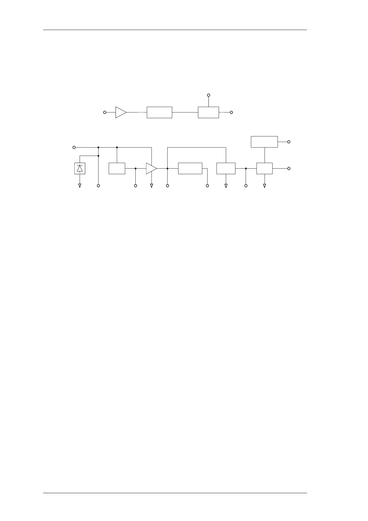
2.5 Audio Processor
(Refer to the audio processor circuit diagram (sheet 2) in Section 6.2 or 6.3.)
Figure 2.6 T856/857 Audio Processor Block Diagram
2.5.1 General
The audio processor comprises several link selectable circuit blocks which may be con-
figured in a variety of combinations to suit individual requirements. The pre-emphasis
network and compressor may be linked individually or cascaded between either or both
audio inputs and the limiter.
Refer to Section 3.5.1 for linking details.
2.5.2 Audio Inputs
Two audio inputs are available: one from a 600 ohm balanced (or unbalanced) line, and
the other from a local microphone. The microphone signal is passed first to a pre-ampli-
fier (Q210) and ultimately to a multiplexer (IC240), but in between may pass through
the compressor (depending on the linking details). The line transformer is also con-
nected to the multiplexer and is disabled by the microphone PTT switch.
A third input for external CTCSS tones is also provided.
Pre-
emphasis
34
6
B
C
5
6
4
34
2
5
3
3
5
7
12
8
N
H
M
I
E
L
J
D
4
6
1
mic.
line
Multiplexer
Inputs
Output
Output
Inhibit
Audio 1 Audio 2
Compressor
Link
Link
Link
Tx Enable
Σ
Carrier
Opto-Key
Tx Key
PTT
Microphone
Input
Line Input
Microphone
Pre-amp.
Opto-coupler
Link
PL205
PL215
PL220
PL210
Limiter
Set Deviation
CTCSS
Low Pass
Filter
Ref. Mod. Adjust
Integrator
Digital Pot.
Digital Pot.
Buffer
Output
To VCO Ref.
Mod.
Constant Current Sink
+
_

M850-00
T856/857 Circuit Operation
C2.9
Copyright TEL 31/09/98
2.5.3 Keying Inputs
There are four ways to key the exciter:
• pulling the Tx-Key line low (pin 13 on D-range 1 [PL100]) at the rear of the set);
• pushing the "Carrier" button on the front panel - this will inhibit all audio;
• using the PTT button on the local microphone, disabling audio from the line;
• via the opto-key inputs (pins 11 and 12 on D-range 1 [PL100]) when electrical
isolation is required. This features a constant current sink (Q270) to ensure reli-
able activation of the opto-coupler (IC250) at low keying voltages.
2.5.4 Compressor (Automatic Level Control (ALC))
The input signal is fed via a current controlled attenuator (Q230, Q220) to a high gain
stage (IC230) from which the output signal is taken. This signal is passed to a compara-
tor (IC230) which toggles whenever the audio signal exceeds a DC threshold deter-
mined by RV220. Thus, the comparator produces a square wave whose mark-space
ratio is determined by the amplitude of the audio signal. This square wave pumps up
the reservoir capacitor (C233) which controls the attenuator (Q230, Q220), thus complet-
ing the feedback loop.
The compression level is set by adjustment of the comparator threshold (RV220).
Note:
Although the high dynamic range of the compressor allows the use of very
low audio signal levels, such conditions will be accompanied by a degrada-
tion of the signal-to-noise ratio. Very low audio input levels should there-
fore be avoided where possible.
2.5.5 Outputs To Modulators
The output signal from the limiter (IC210, IC230) is summed with a CTCSS tone at a
summing amplifier (IC260). The signal is then low pass filtered (IC260) and split to sup-
ply the two modulators.
Since the VCO modulator is a true frequency modulator, its audio is simply buffered
(IC260). The reference modulator, however, is a phase modulator and its audio must
first be integrated (IC210).
It is vital that the audio levels to the modulators are accurately set, relative to each
other. Hence the inclusion of level adjustment in the reference modulator path. Once
set, adjustments to absolute deviation may be made only via the deviation digital pot.
(IC220 - adjustable via PGM800Win).
C2.10
T856/857 Circuit Operation
M850-00
31/09/98 Copyright TEL
2.6 Power Supply & Regulator Circuits
(Refer to the regulators circuit diagram (sheet 6) in Section 6.2 or 6.3.)
Figure 2.7 T856/857 Power Supply & Regulators Block Diagram
The T856 and T857 are designed to operate from a 10.8-16V DC supply (13.8V nominal).
A 5.3V regulator (IC630) runs directly from the 13.8V rail, driving much of the synthe-
siser circuitry. It is also used as the reference for a DC amplifier (IC640, Q630, Q620)
which provides a medium current capability 9V supply. The T856 has a regulator
(IC370) which produces 9V for use in the exciter and audio circuits.
A switching power supply (Q660, Q670) runs from the 9V supply and provides a low
current capability +20V supply. This is used to drive the synthesiser loop filter (IC750),
giving a VCO control voltage range of up to 20V.
Ultimate control of the transmitter is via the Tx-Reg. supply, switched from 9V by Q610.
This is enabled via the Tx-Enable signal from the audio processor, and microprocessor.
Crowbar
Diode LVI
5V
Reg
DC
Amp Switching
PS 5V Dig
Reg
Power
Switch
13.8V
Nom. 5V 5V Dig9V 20V
13.8V Nom.
From Rear
D-Range
Tx Enable
Buffer
Tx Reg.
+9V
µP
Watchdog
Timer
Micro-
controller
µP
Reset
M850-00
T856/857 Circuit Operation
C2.11
Copyright TEL 31/09/98
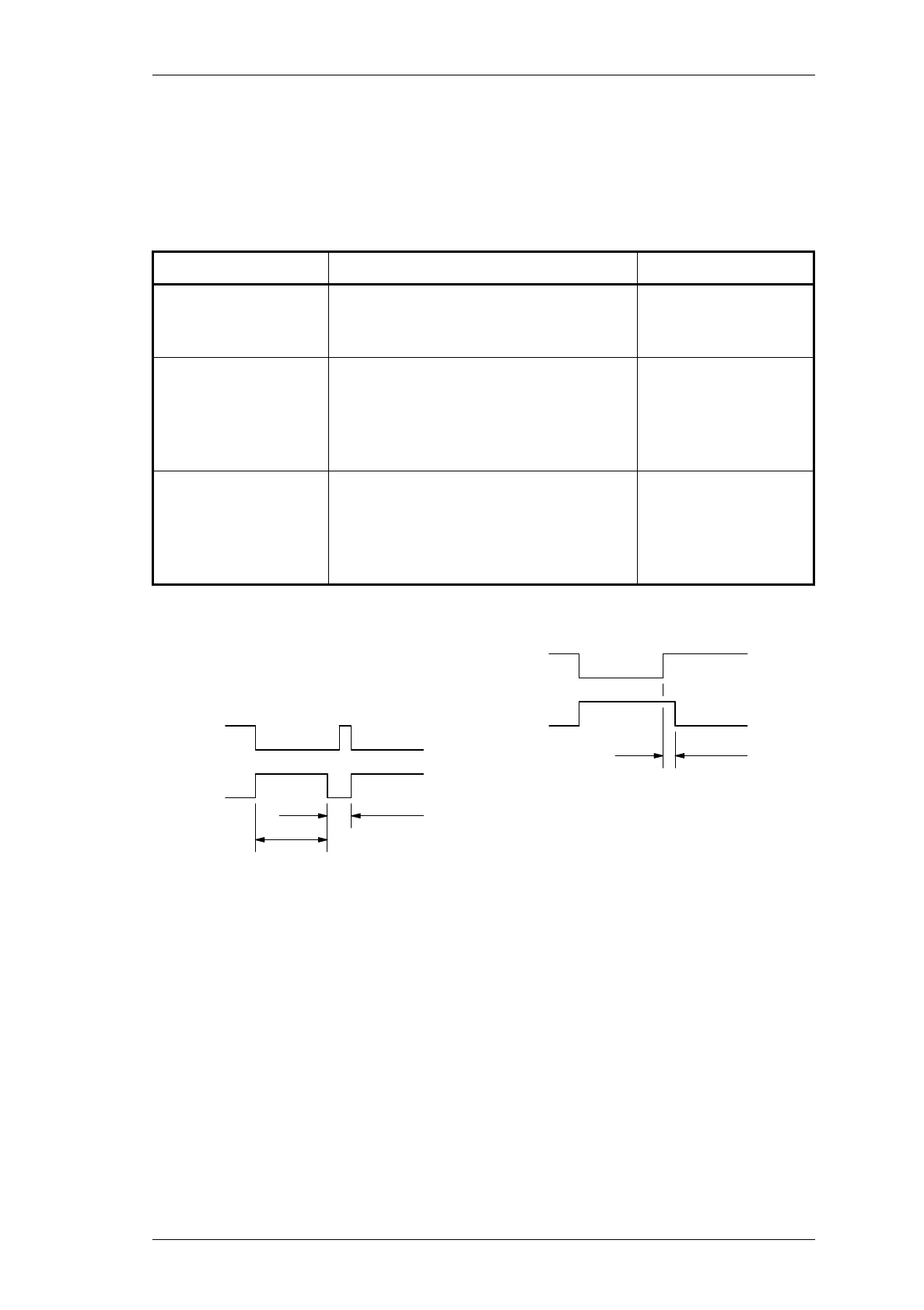
2.7 Transmit Timers
The transmit tail timer, transmit timeout timer and transmit lockout timer can all be set
from PGM800Win. The fields for setting these are found on the system information
page. These three timers operate as follows (refer also to Figure 2.8):
Figure 2.8 T856/857 Transmit Timers
Timer Function Adjustment
Transmit Tail Sets the tail time during which the
transmitter stays keyed after the exter-
nal key source has been removed.
0-5 seconds in 100ms
steps
Transmit Timeout Sets the maximum continuous trans-
mission time. Once the timer has
timed out, the transmitter must be
keyed again, unless prevented by the
transmit lockout timer.
0-300 seconds in 10
second steps
Transmit Lockout Sets the period of time that must
elapse after a timeout before the trans-
mitter can re-transmit. Once the timer
has timed out, the transmitter can be
keyed again.
0-60 seconds in 10
second steps
On
Lockout Time
Timeout
Time
On
Tail Time
Tx-Enable
Tx-Reg.
Tx-Enable
Tx-Reg.

C2.12
T856/857 Circuit Operation
M850-00
31/09/98 Copyright TEL
2.8 T856 Drive Amplifier & PA
(Refer to Figure 2.1 and the exciter and PA circuit diagrams (sheets 3 & 4) in Section 6.2.)
The output power of the PA is maintained at a constant level via a power control loop
applied to the two-stage, wide band exciter amplifier (Q350, Q355). The forward and
reverse RF power levels are sensed via a dual directional coupler and detector diodes
(D440, D420 in the PA cavity). The detected DC signals are buffered (IC330 pins 3 & 5)
and then summed with the ’power control’ level and fed to the control integrator (IC350
pin 6). The output control voltage is buffered by Q310 and Q315, and applied to the col-
lector of the wide band exciter amplifier.
Note:
Forward and reflected power signals are summed so that, under high
VSWR, the power control will turn the output RF level down.
To reduce the spurious output level when the synthesiser is out-of-lock, the Tx-Reg. and
Lock-Detect signals are gated to inhibit the PA control circuit and to switch off the RF
signal at the input to the drive amplifier. This is achieved by a PIN switch attenuator
(D340, D380, D360).
Cyclic keying control is provided by additional circuitry consisting of several time
delay, ramp and gate stages:
• Q325, IC350 power ramping
• Q355, Q325 Tx-Reg. and Lock-Detect gate
• Q335, Q340, Q345 delay and PIN switch drive.
This is to allow the RF power circuits (both exciter and PA) to ramp up and down in a
controlled manner so that minimal adjacent channel interference is generated during
the transition.
The output of the wide band amplifier is approximately 1W (+30dBm) for an input of
100mW (+20dBm) from the VCO, when the power control is set to maximum.
A temperature sensor (R481) is provided so that the RF output power can be reduced to
a preset level when a set temperature is exceeded. This is a protection circuit (IC350 pin
1, Q320) to prevent overheating, as the unit is not rated for continuous operation (refer
to Section 1.2.3 for duty cycle specifications).
#R517, #R518 and #R519 form an attenuator to provide good VCO/exciter isolation as
well as the correct exciter drive level.
The attenuator (#R395, #R396 and #R397) aids in producing the correct exciter drive
level to the PA over the three frequency ranges.
The RF output from the exciter is fed to the driver stage (Q410) and then to the final
(Q420). DC is fed to the final via a low pass filter with special low frequency decou-
pling. CV475 tunes the output matching across the entire band.

M850-00
T856/857 Circuit Operation
C2.13
Copyright TEL 21/06/99
2.9 T857 Exciter Drive Amplifier
(Refer to Figure 2.2 and the exciter circuit diagram (sheet 3) in Section 6.3.)
A two-stage, wide band amplifier (Q304, Q305) provides an output level of approxi-
mately 1W (+30dBm) for an input of 100mW (+20dBm) from the VCO. IC300 pin 1,
Q302, and Q303 provide a 9V regulated supply for the exciter.
To reduce the spurious output level when the synthesiser is out-of-lock, the Tx-Reg. and
Lock-Detect signals are gated to inhibit the exciter control circuit and to switch off the
RF signal at the input to the drive amplifier. This is achieved by a PIN switch attenuator
(D201, D202, D203).
Cyclic keying control is provided by additional circuitry consisting of several time
delay, ramp and gate stages:
• Q301, Q302, Q303, IC300 power ramping
• Q310, Q311 Tx-Reg. and Lock-Detect gate
• Q306, Q307, Q308, Q309 delay and PIN switch drive.
This is to allow the RF power circuits (both exciter and PA) to ramp up and down in a
controlled manner so that minimal adjacent channel interference is generated during
the transition.
R517, R518 and R519 form a 3dB attenuator to provide good VCO/drive amplifier isola-
tion as well as the correct exciter drive level
Note:
The exciter provides a DC control signal to the PA via the RF coax. This is
injected via L314.

C2.14
T856/857 Circuit Operation
M850-00
31/09/98 Copyright TEL
M850-00
T856/857 Initial Tuning & Adjustment
C3.1
Copyright TEL 31/01/99
3 T856/857 Initial Tuning & Adjustment
Caution:
This equipment contains CMOS devices which are susceptible to dam-
age from static charges. Refer to Section 1.2 in Part A for more infor-
mation on anti-static procedures when handling these devices.
The following section describes both short and full tuning and adjustment procedures
and provides information on:
• channel programming
• selecting required audio links
• synthesiser alignment
• PA alignment (T856 only)
• modulator adjustment
• limiter adjustment
• setting line level
• compressor adjustment
• timer adjustment.
Note:
Unless otherwise specified, the term "PGM800Win" used in this and follow-
ing sections refers to version 2.00 and later of the software.
Refer to Figure 4.4 and Figure 4.5 which show the location of the main tuning and
adjustment controls. Refer also to Section 6 where the parts lists, grid reference index
and diagrams will provide detailed information on identifying and locating compo-
nents and test points on the main PCB. The parts list and diagrams for the VCO PCB are
in Part E.
Section Title Page
3.1 Introduction 3.3
3.2 Channel Programming 3.3
3.3 Test Equipment Required 3.4
3.4
3.4.1
3.4.2
3.4.3
3.4.4
3.4.5
3.4.6
3.4.7
Short Tuning Procedure
Introduction
Synthesiser Alignment
Output Power Adjustment (T856 Only)
Two Point Modulation Adjustment
FM Deviation (Limiter) Adjustment
Line-in Level Adjustment
CTCSS Encoder
3.5
3.5
3.5
3.5
3.6
3.6
3.7
3.7

C3.2
T856/857 Initial Tuning & Adjustment
M850-00
31/09/98 Copyright TEL
3.5
3.5.1
3.5.2
Audio Processor Links
Link Details
Typical Options
3.8
3.8
3.8
3.6 Synthesiser Alignment 3.9
3.7 PA Alignment (T856 Only) 3.10
3.8 Thermal Shutdown (T856 Only) 3.10
3.9
3.9.1
3.9.2
3.9.3
3.9.4
3.9.5
3.9.5.1
3.9.5.2
3.9.5.3
Audio Processor
Two Point Modulation
Modulator Adjustment
Limiter Adjustment
Line Level Without Compressor
Compressor
Compressor On Line Input Only
Compressor On Microphone Input Only
Compressor On Both Line & Microphone Inputs
3.11
3.11
3.11
3.12
3.12
3.12
3.12
3.13
3.13
3.10 CTCSS Encoder 3.14
Figure Title Page
3.1
3.2
T856/857 Test Equipment Set-up With T800-01-0010
T856/857 Test Equipment Set-up Without T800-01-0010
3.4
3.4
Section Title Page

M850-00
T856/857 Initial Tuning & Adjustment
C3.3
Copyright TEL 31/09/98
3.1 Introduction
When you receive your T856 transmitter or T857 exciter it will be run up and working
on a particular frequency (the "default channel")1. If you want to switch to a frequency
that is within the 8MHz switching range (i.e. ±4MHz from the factory programmed fre-
quency), you should only need to reprogram the transmitter/exciter with the
PGM800Win software (refer to the PGM800Win programming kit and Section 3.2
below).
However, if you want to switch to a frequency outside the 8MHz switching range, you
will have to reprogram and re-tune the transmitter/exciter to ensure correct operation.
In this case you should carry out the short tuning procedure described in Section 3.4.
If you have carried out repairs or other major adjustments, you must carry out the full
tuning and adjustment procedure described in this section (except for Section 3.4).
3.2 Channel Programming
You can program up to 128 channel frequencies into the transmitter/exciter’s EEPROM
memory (IC820) by using the PGM800Win software package and an IBM PC. You can
also use PGM800Win to select the transmitter/exciter’s current operating frequency (or
"default channel").
If the transmitter/exciter is installed in a rack frame, you can program it via the pro-
gramming port in the speaker panel. However, you can also program the transmitter/
exciter before it is installed in a rack frame as follows:
• by using a T800-01-0010 calibration test unit;
• via D-range 1;
• via D-range 2 (standard T800-03-0000 auxiliary D-range only);
• via SK805 (internal Micromatch connector).
If you do not use the T800-01-0010, you will have to connect the PC to the transmitter/
exciter via a module programming interface (such as the T800-01-0004).
For a full description of the channel programming procedure, refer to the PGM800Win
programming software user’s manual.
Note:
When an auxiliary D-range kit (D-range 2 - T800-03-0000) is fitted, you can
also select a channel with an external switch, such as the DIP switch on the
rack frame backplane PCB. Refer to Part C in the T800 Series Ancillary
Equipment Service Manual (M800-00-101 or later issue) or consult your
nearest Tait Dealer or Customer Service Organisation for further details.
1. Use the "Read Module" function in PGM800Win to find out what the default channel is.

C3.4
T856/857 Initial Tuning & Adjustment
M850-00
31/09/98 Copyright TEL
3.3 Test Equipment Required
You will need the following test equipment:
• computer with PGM800Win installed
• T800 programming kit
• module programming interface (e.g. T800-01-0004 - optional)
• 13.8V power supply
• digital multimeter
• audio signal generator
• RF power meter
• audio voltmeter x 2
• modulation meter
• oscilloscope (digital preferred)
• 20dB or 40dB pad
• T800-01-0010 calibration test unit (optional)
Figure 3.1 and Figure 3.2 show typical test equipment set-ups.
Figure 3.1 T856/857 Test Equipment Set-up With T800-01-0010
Figure 3.2 T856/857 Test Equipment Set-up Without T800-01-0010
or RF test set (optional)
Frequency
Counter
Audio
Voltmeter
RF Power
Meter Oscilloscope
AF O/P
Modulation
Meter
20dB pad: exciter
40dB pad: transmitter
RF O/P
PGM800Win
PSU
+13.8V
-Ve
Audio
Generator
Line I/P
CTCSS I/P
Ω600
Audio
Voltmeter
Exciter/
Transmitter
T800
Calibration
Test Unit
PGM800Win
Serial
Com
PSU
+13.8V
-Ve
Frequency
Counter
Audio
Voltmeter
RF Power
Meter Oscilloscope
AF O/P
Modulation
Meter
20dB pad: exciter
40dB pad: transmitter
Audio
Generator
Line I/P
CTCSS I/P
Ω600
Audio
Voltmeter
Key
RF O/P
Exciter/
Transmitter
via module programming interface
(e.g. T800-01-0004)

M850-00
T856/857 Initial Tuning & Adjustment
C3.5
Copyright TEL 31/09/98
3.4 Short Tuning Procedure
Use this procedure only if you want to reprogram the T856/857 to a frequency outside
the 8MHz switching range and do not intend to carry out any other major adjustments
or repairs.
3.4.1 Introduction
Reprogram the operating frequency as described in the PGM800Win program-
ming kit (refer to Section 3.2).
Remove the top cover (nearest the handle).
Set up the test equipment as described in Section 3.3.
Set the links in the audio processor section as required (refer to Section 3.5).
3.4.2 Synthesiser Alignment
• Connect a high impedance voltmeter to the long lead of L1 in the VCO (this meas-
ures the synthesiser loop voltage).
• Key the transmitter by earthing the Tx-Key line.
•Single Channel Tune VCO trimmer C6 for a synthesiser loop voltage of
10V.
Multichannel Tune VCO trimmer C6 for a synthesiser loop voltage of
10V on the middle channel.
If there is no middle channel, tune C6 so that the channels
are symmetrically placed around a loop voltage of 10V.
All channels should lie within the upper and lower limits
of 16V and 3V respectively.
Do not attempt to program channels with a greater fre-
quency separation than the specified switching range of
8MHz.
3.4.3 Output Power Adjustment (T856 Only)
Connect an RF power meter to the output socket and key the transmitter.
Turn RV310 (power control) fully clockwise.
Tune #CV475 (output power trim) for maximum output power and check that this
is >30W.
Adjust RV310 for the required output power (between 5 and 25W).
Readjust #CV475 to reduce the supply current by up to 0.5A.

C3.6
T856/857 Initial Tuning & Adjustment
M850-00
31/09/98 Copyright TEL
3.4.4 Two Point Modulation Adjustment
Note 1:
In this and following sections deviation settings are given first for wide
bandwidth sets, followed by settings in brackets for mid bandwidth sets ( )
and narrow bandwidth sets [ ].
Note 2:
Reference modulation and limiter adjustment are controlled by
PGM800Win. Electronic potentiometers (256 step) are used to allow chan-
nel-by-channel adjustment of deviation and two point modulation.
Note 3:
To optimise the modulation response across the switching range, repeat
steps 1-4 below for each channel that will be used (usually needed only for
data applications). In applications where the modulation response is less
critical (e.g. voice use only), carry out steps 1-4 below on the middle channel
and cut and paste the value to all other channels.
1. Inject an audio signal of 300Hz 1.5V rms (+5dBm) into the CTCSS input (D-range
1 (PL100) pin 8).
Key the transmitter by earthing the Tx-Key line.
2. Adjust the output from the audio generator to obtain ±3kHz (±2.4kHz) [±1.5kHz]
deviation at 300Hz.
3. Change the input frequency to 100Hz and adjust IC220 via PGM800Win “refer-
ence modulation” to obtain ±3kHz (±2.4kHz) [±1.5kHz] deviation (you can use
either the mouse or up and down arrow keys).
4. Change the input frequency back to 300Hz.
Repeat steps 2 and 3 above until the deviations achieved at the two input frequen-
cies are within 0.2dB of each other. You will need to do this at least four times.
5. Sweep the audio between 50 and 300Hz for peaks.
Note:
A peak between 50 and 300Hz will indicate a fault condition, i.e:
- incorrect set-up
or - modulation circuitry fault.
The specification window is ±1dB relative to 150Hz from 67 to 260Hz.
3.4.5 FM Deviation (Limiter) Adjustment
Note:
If the T856/857 will be used over the whole 8MHz switching range, you
must set the deviation for each channel. However, if the module will be
used on frequencies that cover only a 1MHz (or less) switching range, you
can set the deviation on the middle channel and use this value for all other
channels with the “fill” option in PGM800Win.
Inject 1kHz at -10dBm into the line input (D-range 1 (PL100) pins 1 & 4; pins 2 & 3
shorted; refer to Section 2.2 of Part F).

M850-00
T856/857 Initial Tuning & Adjustment
C3.7
Copyright TEL 31/09/98
Adjust RV210 (line sensitivity) fully clockwise and key the transmitter by earthing
the Tx-Key line. Adjust IC220 via PGM800Win “deviation” to set the peak devia-
tion to ±4.7kHz (±3.8kHz) [±2.3kHz] (you can use either the mouse or up and
down arrow keys).
Sweep the audio frequency from 100Hz to 4kHz and ensure that the maximum
deviation does not exceed ±4.7kHz (±3.8kHz) [±2.3kHz]. Readjust IC220 if neces-
sary via PGM800Win “deviation”.
3.4.6 Line-in Level Adjustment
Set the injected signal at the line input to the required line level (typically -10 to
-20dBm).
Adjust RV210 (line sensitivity) to provide ±3kHz (±2.4kHz) [±1.5kHz] deviation.
3.4.7 CTCSS Encoder
Program a CTCSS tone on the set channel using PGM800Win.
Key the T856/857 with the front panel "Carrier" switch.
Adjust RV805 (CTCSS level adjust) to give 10% system deviation.
Reset the maximum deviation as per Section 3.4.5.

C3.8
T856/857 Initial Tuning & Adjustment
M850-00
31/09/98 Copyright TEL
3.5 Audio Processor Links
3.5.1 Link Details
Use the following table to set up the audio processor to the configuration you require.
You should set the audio processor links before carrying out any of the tuning and
adjustment procedures. The factory settings are shown in brackets [ ].
3.5.2 Typical Options
Plug Linka
a. The letters in this column and in the table in Section 3.5.2 below refer to the identification
letters screen printed onto the PCB beside each pair of pins.
Function
PL205
1-2
[3-4]
5-6
A
B
C
not connected
microphone pre-amp. output to compressor input
microphone pre-amp. output to multiplexer input
PL210
[1-2]
3-4
5-6
L
M
N
multiplexer output to pre-emphasis input
multiplexer output to limiter input
multiplexer output to compressor input
PL215
1-2
[3-4]
5-6
7-8
9-10
G
H
I
J
K
not connected
compressor output to multiplexer input
compressor output to limiter input
compressor output to pre-emphasis input
not connected
PL220
1-2
[3-4]
5-6
D
E
F
pre-emphasis output to multiplexer input
pre-emphasis output to limiter input
not connected
PL205 PL210 PL215 PL220
microphone pre-amp. compressed
and pre-emphasised;
line input pre-emphasised
(standard set-up)
[3-4]
B
[1-2]
L
[3-4]
H
[3-4]
E
microphone pre-amp. compressed
and pre-emphasised;
line input unprocessed
3-4
B
3-4
M
7-8
J
1-2
D
line and microphone compressed
and pre-emphasised
5-6
C
5-6
N
7-8
J
3-4
E
microphone pre-amp. compressed;
line and microphone flat response
3-4
B
3-4
M
3-4
H
5-6
F

M850-00
T856/857 Initial Tuning & Adjustment
C3.9
Copyright TEL 31/09/98
3.6 Synthesiser Alignment
• Ensure that the T856/857 has been programmed with the required frequencies
using PGM800Win software.
•Single Channel Select a channel using PGM800Win.
Multichannel Select the middle channel via PGM800Win.
• Connect a high impedance voltmeter to the long lead of L1 in the VCO (this meas-
ures the synthesiser loop voltage).
• Key the transmitter by earthing the Tx-Key line.
Single Channel Tune VCO trimmer C6 for a synthesiser loop voltage of
10V.
Multichannel Tune VCO trimmer C6 for a synthesiser loop voltage of
10V on the middle channel.
If there is no middle channel, tune C6 so that the channels
are symmetrically placed around a loop voltage of 10V.
All channels should lie within the upper and lower limits
of 16V and 3V respectively.
Do not attempt to program channels with a greater fre-
quency separation than the specified switching range
(8MHz).
• Check that the exciter output power is 1W ±300mW (T857 only).
• Measure the exciter output frequency and adjust the TCXO (=IC700) trimmer if
required.
Caution:
This trimmer is susceptible to physical damage. Do not exert a down-
ward force of more than 500g (1lb) when adjusting.

C3.10
T856/857 Initial Tuning & Adjustment
M850-00
31/09/98 Copyright TEL
3.7 PA Alignment (T856 Only)
Check that the exciter is connected to the PA with the coaxial link.
Connect an RF power meter to the PA output (use an appropriate attenuator as
necessary).
Turn RV310 (power control) fully clockwise.
Note:
Before the following measurement is taken, ensure the heatsink is at ambi-
ent temperature (20-25°C).
Measure and record the voltage (VL) at L481; perform this measurement at room
temperature so that the NTC (R481) is close to 25°C.
Key the transmitter by earthing the Tx-Key line.
Tune #CV475 until maximum power is obtained. Check that the power exceeds
30W.
Adjust RV310 (power control) to 25W.
Readjust #CV475 to reduce the supply current by up to 0.5A.
3.8 Thermal Shutdown (T856 Only)
Key the transmitter by earthing the Tx-Key line and set the output power to 25W
as described in Section 3.7.
Short L481 to ground.
Set RV330 (shutdown power level) for an output power of 5W.
Set RV320 (shutdown temperature) to 0.16VL volts (measured at IC350 pin 3),
where VL is the voltage measured at L481 in Section 3.7. This sets the thermal
shutdown at 85°C at NTC R481.

M850-00
T856/857 Initial Tuning & Adjustment
C3.11
Copyright TEL 31/09/98
3.9 Audio Processor
3.9.1 Two Point Modulation
The T856 and T857 utilise two point modulation to obtain a wide audio bandwidth
independent of the synthesiser loop filter response. This is achieved by simultaneously
frequency modulating the VCO and phase modulating the synthesiser reference fre-
quency. The relative signal levels fed to the two modulators are quite critical and cause
interaction when setting up.
Both modulating signals require readjustment when the exciter is shifted in frequency
greater than the switching range (i.e. ∆F>±4MHz).
Note 1:
In this and following sections deviation settings are given first for wide
bandwidth sets, followed by settings in brackets for mid bandwidth sets ( )
and narrow bandwidth sets [ ].
Note 2:
Reference modulation and limiter adjustment are controlled by
PGM800Win. Electronic potentiometers (256 step) are used to allow chan-
nel-by-channel adjustment of deviation and two point modulation.
Note 3:
To optimise the modulation response across the switching range, repeat
steps 1-4 below for each channel that will be used (usually needed only for
data applications). In applications where the modulation response is less
critical (e.g. voice use only), carry out steps 1-4 below on the middle channel
and cut and paste the value to all other channels.
3.9.2 Modulator Adjustment
1. Inject an audio signal of 300Hz 1.5V rms (+5dBm) into the CTCSS input (D-range
1 (PL100) pin 8).
Key the transmitter by earthing the Tx-Key line.
2. Adjust the output from the audio generator to obtain ±3kHz (±2.4kHz) [±1.5kHz]
deviation at 300Hz.
3. Change the input frequency to 100Hz and adjust IC220 via PGM800Win “refer-
ence modulation” to obtain ±3kHz (±2.4kHz) [±1.5kHz] deviation.
4. Change the input frequency back to 300Hz.
Repeat steps 2 and 3 above until the deviations achieved at the two input frequen-
cies are within 0.2dB of each other. You will need to do this at least four times.
5. Sweep the audio between 50 and 300Hz for peaks.
Note:
A peak between 50 and 300Hz will indicate a fault condition, i.e:
- incorrect set-up
or - modulation circuitry fault.
The specification window is ±1dB relative to 150Hz from 67 to 260Hz.

C3.12
T856/857 Initial Tuning & Adjustment
M850-00
31/09/98 Copyright TEL
3.9.3 Limiter Adjustment
Note:
If the T856/857 will be used over the whole 8MHz switching range, you
must set the deviation for each channel. However, if the module will be
used on frequencies that cover only a 1MHz (or less) switching range, you
can set the deviation on the middle channel and use this value for all other
channels with the “fill” option in PGM800Win.
Set the links in the audio processor section as required (refer to Section 3.5).
Inject 1kHz at -10dBm into the line input (D-range 1 (PL100) pins 1 & 4; and pins 2
& 3 shorted; refer to Section 2.2 of Part F).
Adjust RV210 (line sensitivity) fully clockwise and key the transmitter by earthing
the Tx-Key line. Adjust IC220 via PGM800Win “deviation” to set the peak devia-
tion to ±4.7kHz (±3.8kHz) [±2.3kHz] (you can use either the mouse or up and
down arrow keys).
Sweep the audio frequency from 100Hz to 4kHz and ensure that the maximum
deviation does not exceed ±4.7kHz (±3.8kHz) [±2.3kHz]. Readjust IC220 if neces-
sary via PGM800Win “deviation”.
3.9.4 Line Level Without Compressor
This section assumes that the compressor is not used. If the compressor is required,
refer to Section 3.9.5.
Adjust the line sensitivity as follows:
• set the injected signal at the line input to the required line level (typically -10 to
-20dBm);
• adjust RV210 (line sensitivity) to provide ±3kHz (±2.4kHz) [±1.5kHz] devia-
tion.
3.9.5 Compressor
The compressor may be used on the line input only, the microphone input only, or on
both the line and microphone inputs. If the compressor is used, refer to one of the fol-
lowing sections as appropriate.
3.9.5.1 Compressor On Line Input Only
Set RV210 (line sensitivity) fully clockwise and key the transmitter by earthing the
Tx-Key line.
Reduce the line level to -50dBm at 1kHz and set RV220 (compression level) fully
clockwise.

M850-00
T856/857 Initial Tuning & Adjustment
C3.13
Copyright TEL 31/09/98
Check that ±3kHz deviation (±2.4kHz) [±1.5kHz] is still available.
Slowly increase the audio input level until the demodulated waveform shows sig-
nificant signs of clipping (approximately ±4.5kHz (±3.6kHz) [±2.3kHz] deviation).
Adjust RV220 anticlockwise until the demodulated waveform is just clipping
(approximately ±4kHz (±3.2kHz) [±2kHz] deviation).
Increase the input level to -10dBm and check that the test tone is still held just into
clipping. The input line level should be typically -10 to -20dBm.
3.9.5.2 Compressor On Microphone Input Only
Key the transmitter by earthing the Tx-Key line and plug a microphone jack into
the front panel socket.
Adjust RV220 (compression level) fully clockwise.
Acoustically couple the microphone to a tone box (1kHz) and close the PTT
switch.
Increase the audio level until the demodulated waveform shows significant signs
of clipping (approximately ±4.5kHz (±3.6kHz) [±2.3kHz] deviation).
Adjust RV220 anticlockwise until the demodulated waveform is just clipping
(approximately ±4kHz (±3.2khz) [±2kHz] deviation).
Increase the audio level by 10dB and verify that the test tone is held just into clip-
ping.
Whistle steadily into the microphone, checking that approximately ±4kHz
(±3.2khz) [±2kHz] deviation is produced. The modulated waveform should be
basically sinusoidal.
Speak into the microphone, checking that the modulation peaks reach about
±5kHz (±4kHz) [±2.5kHz] deviation.
As the line is to be used without compression, set RV210 (line sensitivity) as
described in Section 3.9.4.
3.9.5.3 Compressor On Both Line & Microphone Inputs
Set up as described in Section 3.9.5.1.

C3.14
T856/857 Initial Tuning & Adjustment
M850-00
31/09/98 Copyright TEL
3.10 CTCSS Encoder
Program a CTCSS tone on the set channel using PGM800Win.
Key the T856/857 with the front panel "Carrier" switch.
Adjust RV805 (CTCSS level adjust) to give 10% system deviation.
Reset the maximum deviation as per Section 3.9.3.
M850-00
T856/857 Functional Testing
C4.1
Copyright TEL 31/09/98
4 T856/857 Functional Testing
Caution:
This equipment contains CMOS devices which are susceptible to dam-
age from static charges. Refer to Section 1.2 in Part A for more infor-
mation on anti-static procedures when handling these devices.
The following test procedures will confirm that the T856/857 has been tuned and
adjusted correctly and is fully operational.
Note 1:
In this and following sections deviation settings are given first for wide
bandwidth sets, followed by settings in brackets for mid bandwidth sets ( )
and narrow bandwidth sets [ ].
Note 2:
Unless otherwise specified, the term "PGM800Win" used in this and follow-
ing sections refers to version 2.00 and later of the software.
Refer to Figure 4.4 and Figure 4.5 for the location of the main tuning and adjustment
controls, and to Section 3.3 for the test equipment set-up. Refer also to Section 6 where
the parts lists, grid reference index and diagrams will provide detailed information on
identifying and locating components and test points on the main PCB. The parts list
and diagrams for the VCO PCB are in Part E.
The following topics are covered in this section.
Section Title Page
4.1 Current Consumption 4.3
4.2 Output Power 4.3
4.3 Output Frequency 4.3
4.4 Timers 4.3
4.5 Frequency Response 4.4
4.6 Audio Level Input Sensitivity 4.7
Figure Title Page
4.1
4.2
4.3
4.4
4.5
T856/857 Transmit Timers
T856/857 Pre-emphasis Response
T856/857 Limiting Response
T856 Main Tuning & Adjustment Controls
T857 Main Tuning & Adjustment Controls
4.4
4.5
4.6
4.9
4.11

C4.2
T856/857 Functional Testing
M850-00
31/09/98 Copyright TEL

M850-00
T856/857 Functional Testing
C4.3
Copyright TEL 31/09/98
4.1 Current Consumption
Connect the T856/857 to a 13.8V power supply.
Connect an RF power meter to the T856/857 output socket.
Check that the current in the 13.8V power cable is less than 150mA.
Key the T856/857 by earthing the Tx-Key line (the carrier "On" LED should light).
T856 Only: Adjust RV310 (power control) to obtain 25W output power.
Check that the current is as follows:
T856 <5.5A
T857 <750mA.
4.2 Output Power
Connect an RF power meter with suitable attenuation to the T856/857 output
socket.
Key the T856/857 by earthing the Tx-Key line.
Check that:
T856 the output power adjusts to ≥25W with RV310 (power control)
turned fully clockwise
T857 the output power is 1W ±300mW.
4.3 Output Frequency
Connect the T856/857 output to a frequency counter via an attenuator pad:
T856 40dB pad
T857 20dB pad.
Measure the output frequency and, if necessary, adjust the TCXO (=IC700) to trim
to the nominal frequency (±100Hz).
4.4 Timers
The transmit tail timer, transmit timeout timer and transmit lockout timer can all
be set from PGM800Win. The fields for setting these are found on the system
information page. These three timers operate as follows (refer also to Figure 4.1):
C4.4
T856/857 Functional Testing
M850-00
31/09/98 Copyright TEL
Figure 4.1 T856/857 Transmit Timers
4.5 Frequency Response
If the T856/857 has been correctly adjusted, the pre-emphasis and limiting responses
should closely match those shown in Figure 4.2 and Figure 4.3 respectively.
Note:
The limits shown on these graphs should not be exceeded.
• Measure the pre-emphasis response as follows:
Reduce the line level to give ±1kHz (±0.8kHz) [±0.5kHz] deviation at 1kHz.
Sweep the modulation frequency.
The response should closely match that shown in Figure 4.2.
• Measure the limiting response as follows:
Set the line level to give ±3kHz (±2.4kHz) [±1.5kHz] deviation at 1kHz.
Increase the line level 20dB and sweep the modulation frequency.
The response should closely match that shown in Figure 4.3.
Timer Function Adjustment
Transmit Tail Sets the tail time during which the
transmitter stays keyed after the exter-
nal key source has been removed.
0-5 seconds in 100ms
steps
Transmit Timeout Sets the maximum continuous trans-
mission time. Once the timer has
timed out, the transmitter must be
keyed again, unless prevented by the
transmit lockout timer.
0-300 seconds in 10
second steps
Transmit Lockout Sets the period of time that must
elapse after a timeout before the trans-
mitter can re-transmit. Once the timer
has timed out, the transmitter can be
keyed again.
0-60 seconds in 10
second steps
On
Lockout Time
Timeout
Time
On
Tail Time
Tx-Enable
Tx-Reg.
Tx-Enable
Tx-Reg.
M850-00
T856/857 Functional Testing
C4.5
Copyright TEL 31/09/98
Figure 4.2 T856/857 Pre-emphasis Response
Wide Bandwidth
Narrow Bandwidth
Mid Bandwidth
The mid bandwidth graph is the same shape as the wide bandwidth graph. The devia-
tion figures are as follows:
peak + max. deviation = +0.8kHz
peak - max. deviation = -0.8kHz.
+10
+8
Modulation Level (dB ref. to dev. @ 1kHz)
+6
+4
+2
+0
-2
-4
-6
-8
-10
-12
-14
-16
-18
-20
-22
100 200 300 500 1k 2k 3k 5k 10k
Frequency (Hz)
Peak + max. dev. = +1.0kHz @ 1000Hz
Peak - max. dev. = -1.0kHz @ 1000Hz
+10
+8
Modulation Level (dB ref. to dev. @ 1kHz)
+6
+4
+2
+0
-2
-4
-6
-8
-10
-12
-14
-16
-18
-20
-22
100 200 300 500 1k 2k 3k 5k 10k
Frequency (Hz)
Peak + max. dev. = +0.5kHz @ 1000Hz
Peak - max. dev. = -0.5kHz @ 1000Hz

C4.6
T856/857 Functional Testing
M850-00
31/09/98 Copyright TEL
Figure 4.3 T856/857 Limiting Response
Wide Bandwidth
Narrow Bandwidth
100 500300 5k50
+10
+8
Modulation Level (dB ref. to max. dev.)
+6
+4
+2
+0
-2
-4
-6
-8
-10
-12
-14
-16
-18
-20
-22
10 20 30 200 1k 2k 3k 10k
Frequency (Hz)
Peak + max. dev. = +4.9kHz @ 1500Hz
Peak - max. dev. = -4.4kHz @ 2500Hz
Above limiting (steady-state)
Mid Bandwidth
The mid bandwidth graph is the same shape as the wide bandwidth graph. The devia-
tion figures are as follows:
peak + max. deviation = +4kHz
peak - max. deviation = -4kHz.
100 500300 5k50
+10
+8
Modulation Level (dB ref. to max. dev.)
+6
+4
+2
+0
-2
-4
-6
-8
-10
-12
-14
-16
-18
-20
-22
10 20 30 200 1k 2k 3k 10k
Frequency (Hz)
Peak + max. dev. = +2.4kHz @ 2000Hz
Peak - max. dev. = -2.5kHz @ 2000Hz
Above limiting (steady-state)

M850-00
T856/857 Functional Testing
C4.7
Copyright TEL 31/09/98
4.6 Audio Level Input Sensitivity
• Adjust RV210 (line sensitivity) fully clockwise.
• Check that the input sensitivities are better than those specified below:
Note:
A degraded signal to noise ratio can be expected with the compressor
selected. The extent of the degradation is dependent on the audio input
level.
Line Input 600 ohms, ±3kHz (±2.4kHz) [±1.5kHz] deviation at
1kHz:
with compressor -50dBm
without compressor -30dBm
Microphone Input 600 ohms, ±3kHz (±2.4kHz) [±1.5kHz] deviation at
1kHz:
with compressor -75dBm
without compressor -55dBm
CTCSS Input 1kHz deviation at 150Hz 500mV rms

C4.8
T856/857 Functional Testing
M850-00
31/09/98 Copyright TEL
M850-00
T856/857 Fault Finding
C5.1
Copyright TEL 31/09/98
5 T856/857 Fault Finding
Caution:
This equipment contains CMOS devices which are susceptible to dam-
age from static charges. Refer to Section 1.2 in Part A for more infor-
mation on anti-static procedures when handling these devices.
The following test procedures and fault finding flow charts may be used to help locate a
hardware problem, however they are by no means a complete fault finding procedure.
If you still cannot trace the fault after progressing through them in a logical manner,
contact your nearest Tait Dealer or Customer Service Organisation. If necessary, you can
get additional technical help from Customer Support, Radio Systems Division, Tait Elec-
tronics Ltd, Christchurch, New Zealand (full contact details are on page 2).
Note 1:
In this and following sections deviation settings are given first for wide
bandwidth sets, followed by settings in brackets for mid bandwidth sets ( )
and narrow bandwidth sets [ ].
Note 2:
Unless otherwise specified, the term "PGM800Win" used in this and follow-
ing sections refers to version 2.00 and later of the software.
Refer to Section 6 where the parts lists, grid reference index and diagrams will provide
detailed information on identifying and locating components and test points on the
main PCB. The parts list and diagrams for the VCO PCB are in Part E.
The following topics are covered in this section
Section Title Page
5.1 Visual Checks 5.3
5.2 Component Checks 5.3
5.3 Front Panel LED Indicator 5.3
5.4
5.4.1
5.4.2
DC Checks
Power Rails
VCO Locking
5.4
5.4
5.4
5.5
5.5.1
5.5.2
5.5.3
5.5.4
RF Checks
T856 Drive Power
T856 PA Output Power
T857 Output Power
Audio And Modulation
5.5
5.5
5.5
5.5
5.6
5.6 PGM800Win Generated Errors 5.7

C5.2
T856/857 Fault Finding
M850-00
31/09/98 Copyright TEL
5.7
5.7.1
5.7.1.1
5.7.1.2
5.7.1.3
5.7.2
5.7.3
5.7.4
5.7.5
5.7.6
5.7.7
Fault Finding Charts
Microcontroller
Basic Checks
Serial Communications
CTCSS Encode
Regulator
Synthesiser
T856 Drive Amplifier
T856 PA & Power Control
T857 Exciter Drive Amplifier
Audio Processor
5.8
5.8
5.8
5.9
5.10
5.11
5.12
5.15
5.16
5.17
5.18
5.8 To Replace The T856 PA Transistors (Q410 & Q420) 5.19
Figure Title Page
5.1
5.2
RF Diode Probe Circuit
Typical Transistor/Capacitor Spacing (Not To Scale)
5.5
5.19
Section Title Page
M850-00
T856/857 Fault Finding
C5.3
Copyright TEL 31/09/98
5.1 Visual Checks
Remove the covers from the T856/857 and inspect the PCB for damaged or broken com-
ponents, paying particular attention to the surface mounted devices (SMD's).
Check for defective solder joints. If repair or replacement is considered necessary, refer
to Section 3 of Part A.
5.2 Component Checks
If you suspect a transistor is faulty, you can assess its performance by measuring the for-
ward and reverse resistance of the junctions. Unless the device is completely desol-
dered, first make sure that the transistor is not shunted by some circuit resistance. Use a
good quality EVM (e.g. Fluke 75) for taking the measurements (or a 20k ohm/V or bet-
ter multimeter, using only the medium or low resistance ranges).
The collector current drawn by multi-junction transistors is a further guide to their per-
formance.
If an IC is suspect, the most reliable check is to measure the DC operating voltages. Due
to the catastrophic nature of most IC failures, the pin voltages will usually be markedly
different from the recommended values in the presence of a fault. The recommended
values can be obtained from either the circuit diagram or the component data catalogue.
5.3 Front Panel LED Indicator
The green "Supply" LED on the T856/857 front panel will flash according to the condi-
tions described in the following table:
Where two or more conditions occur at the same time, the precedence is in the order
shown above (i.e. T856/857 linked has the highest priority, followed by internal error).
Flash Rate Condition
fast ( sec. on/ sec. off
approx.) T856/857 is linked with
PGM800Win
unequal ( sec. on/1 sec. off
approx.) microcontroller has detected an
internal communications error -
refer to Section 5.7.1

C5.4
T856/857 Fault Finding
M850-00
31/09/98 Copyright TEL
5.4 DC Checks
5.4.1 Power Rails
Refer to the test points and options diagrams in Section 6 for test point locations, and to
the regulator fault finding chart (Section 5.7.2) for fault diagnosis.
Check the 13.8V (TP601) and 9V (TP602) supplies at their test points in the regula-
tor compartment with a DMM.
Check the 5V (TP604) and 20V (TP603) rails at their respective test points in the
regulator compartment.
Check that Tx-Reg. (TP305 in the exciter compartment) comes up to 8.8V when the
exciter is keyed.
Check the +5V digital regulator output (TP607 in the regulator compartment).
T856 Only: Check the 9V supply (IC370 pin 1) with a DMM.
Check for short circuits.
5.4.2 VCO Locking
Key the exciter.
Using a DMM, monitor the VCO control voltage on the long lead of L1 on the
VCO PCB.
If the synthesiser is locked and the VCO aligned, the voltage at this point should
be between 3 and 16V.
If the VCO is not locked, refer to the synthesiser fault finding chart (Section 5.7.3).
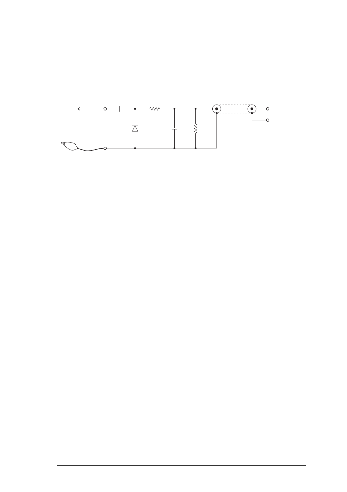
M850-00
T856/857 Fault Finding
C5.5
Copyright TEL 31/09/98
5.5 RF Checks
In-circuit RF levels may be measured with an RF probe on which the earth lead has been
shortened to a minimum (i.e. 13mm). Refer to the circuit diagrams for typical levels.
Figure 5.1 shows a suitable RF probe circuit..
Figure 5.1 RF Diode Probe Circuit
5.5.1 T856 Drive Power
Refer to the drive amplifier fault finding chart (Section 5.7.4).
Ensure that the VCO locks (refer to Section 5.4.2).
Connect the drive output to a power meter and key the transmitter.
Check that the exciter output power (SK310) is >1.5W.
Note:
If the synthesiser is out of lock, the lock detector (synthesiser IC740 and
comparator IC750) will prevent the RF signal from reaching the PA by
switching the supply to the exciter amplifier (Q350, Q355).
5.5.2 T856 PA Output Power
Reconnect the drive output to the PA input.
Connect the PA to a power meter and key the transmitter.
Check that the output power is >30W with RV310 (power control) adjusted fully
clockwise.
5.5.3 T857 Output Power
Refer to the exciter drive amplifier fault finding chart (Section 5.7.6).
Ensure that the VCO locks (refer to Section 5.4.2).
100k
10k
1n
1n
1N6263
Coax
Probe
Earthing Clip
DC to DVM or
Oscilloscope
This unit is not suitable for use on high power RF circuits.

C5.6
T856/857 Fault Finding
M850-00
31/09/98 Copyright TEL
Connect the exciter output to a power meter and key the exciter.
Check that the output power is 1W ±300mW.
Note:
If the synthesiser is out of lock, the lock detector (synthesiser IC740 and
comparator IC750) will prevent the RF signal from reaching the PA by
switching the supply to the exciter amplifier (Q301, IC300, Q302, Q303).
5.5.4 Audio And Modulation
Refer to the audio processor fault finding chart (Section 5.7.7).
Set up the audio processor as described in Section 3.9.
Check that the demodulated RF output has the frequency response referred to in
Section 4.5 with at least ±5kHz (±4kHz) [±2.5kHz] deviation available at 1kHz
modulating frequency.
If the above result is not achieved, either the two modulators are incorrectly adjusted or
a fault condition exists.

M850-00
T856/857 Fault Finding
C5.7
Copyright TEL 31/09/98
5.6 PGM800Win Generated Errors
The following errors are those most likely to occur using PGM800Win. Refer to the
PGM800Win software user’s manual for a complete list of error messages.
Channel Switch Set
The programmed default channel change was not accepted by the base station because a
channel is selected externally. Try turning the external channel switch off to change the
default channel in PGM800Win.
Synth Out Of Lock
The synthesiser received incorrect data, or the data was corrupted. Enter a frequency
within the VCO switching range, or tune the VCO.
Internal Error
Data could not be read from the base station due to an internal error. Check for shorts or
open circuits on the SDA, SCK, SYNTH and EPOT lines. The SDA, SCK and SYNTH
are normally high, and the EPOT is normally low.
Write/Read To An Unlinked Module
The link to the module does not exist. Undefined error.
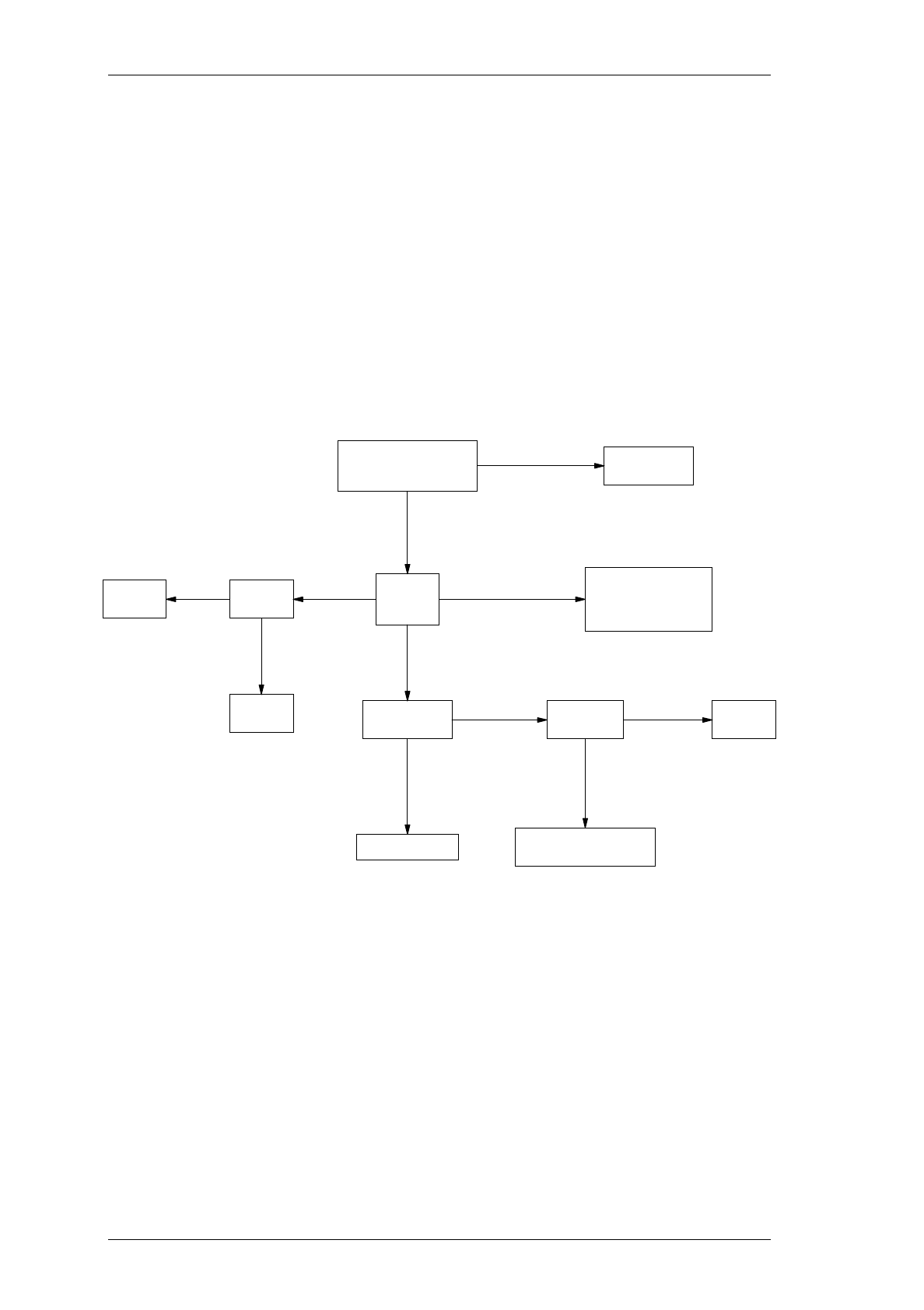
C5.8
T856/857 Fault Finding
M850-00
31/09/98 Copyright TEL
5.7 Fault Finding Charts
Note:
The standard test point designations used in this section are as follows:
TP601 13.8V
TP602 9V
TP603 20V
TP604 5V
5.7.1 Microcontroller (IC810)
5.7.1.1 Basic Checks
Pulsing Check state
of pin 35.
Y
Is pin 30
pulsing?
High or open circuit
Y
Static high/low
Check state of
pins 36 to 43.
Low/floating
High
Is the 12.8MHz clock
present on IC810 pin 21
(microcontroller)?
N
Replace
IC810.
Check IC740
(synthesiser).
*digital storage oscilloscope
Replace IC810.
Check the
state of
pin 10.
N Pulsing
Low
Replace
IC810.
Use a DSO* to check
operation of IC650
(i.e. active high
pulse at power up).
Replace
IC650.
Correct the fault causing
pin 35 to be low/floating.

M850-00
T856/857 Fault Finding
C5.9
Copyright TEL 31/09/98
5.7.1.2 Serial Communication
Check pin state.
Y
Low/floatin
g
N
Noise
on pin
Disconnect the
pro
g
rammin
g
lead.
Is IC810 pin 11 hi
g
h?
(microcontroller)
Y*di
g
ital stora
g
e
oscilloscope
Use PGM800Win
to send a POLL
command to the
radio.
Check the transistor
interface circuitry
and/or replace the
pro
g
rammin
g
lead.
Check the SERIAL-COM
and AUDIO-1/2 links.
Replace
IC810.
Check the transistor
interface circuitry
and/or replace the
pro
g
rammin
g
lead.
Check the transistor
interface circuitry.
Check IC810 pin 13
with a DSO. Is there
a response from IC810 after
a poll command is sent?
N
Y
Connect the pro
g
rammin
g
lead and use PGM800Win
to read the rack/radio.
Check I/O pad P810
with a DSO*.
Does it swin
g
from
0 to 5V?
N
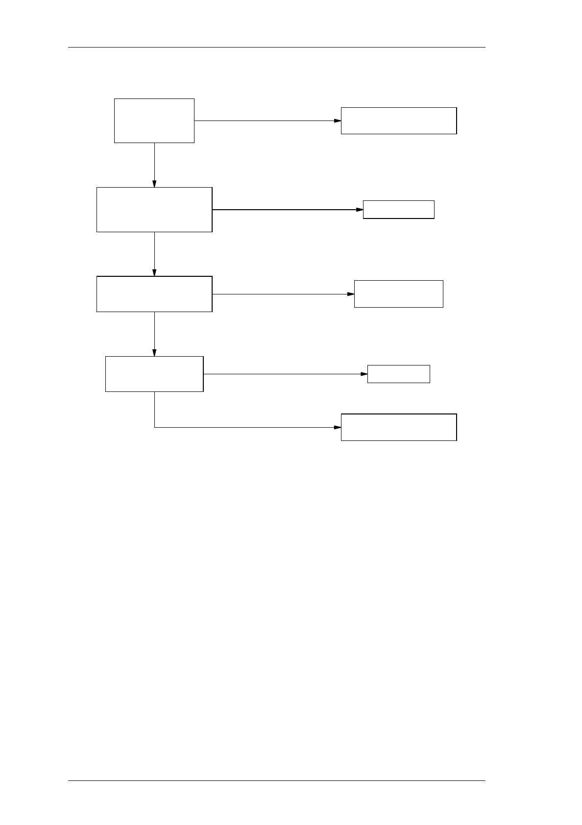
C5.10
T856/857 Fault Finding
M850-00
31/09/98 Copyright TEL
5.7.1.3 CTCSS Encode
Y
Y
Y
Replace IC810.
Use PGM800Win to
select a channel
with a CTCSS tone
pro
g
rammed.
Check serial communications.
(See separate flow chart).
Cannot select a channel
Check IC810 pins 24, 25
& 26 (microcontroller).
Are there 5V square waves at
the CTCSS frequency?
Check IC830 pins 1, 7 & 14.
Are there 9V square waves at
the CTCSS frequency?
Check IC830 pin 8.
Is there a sine wave
at the CTCSS frequency? Check RV805.
No tone
Check the filter circuit for bias
problems and/or short circuits.
Distorted tone
No square waves or
uneven mark/space ratio
No square waves or
uneven mark/space ratio Check IC830 circuitry
and repair/replace.

M850-00
T856/857 Fault Finding
C5.11
Copyright TEL 31/09/98
5.7.2 Regulator
N
Y
Check for
overheatin
g
components &
short circuits.
N
Y
Check Q630,
Q620 & IC640.
N
Y
9.0V present
on TP602?
Check Q660 is
switchin
g
at
approx. 150kHz.
N
Y
20V present
on TP603?
Check R615.
Replace IC610.
N
Y
+5V present on
IC610 pin 2?
Key Tx.
YRe
g
ulators OK.
N
8.8V present
on Tx re
g
. TP305?
Replace Q610.
Y
N
0V present
on Q860 collector?
Check Q860 and
associated circuitry.
Y
0.6V present on
Q860 base?
N
Re
g
ulators OK.
Check microcontroller
section.
Check continuity
from pin 9 of
D-ran
g
e 1.
13.8V present on
IC630 pin 3?
5.3V present on
IC630 pin 1? Replace IC630.
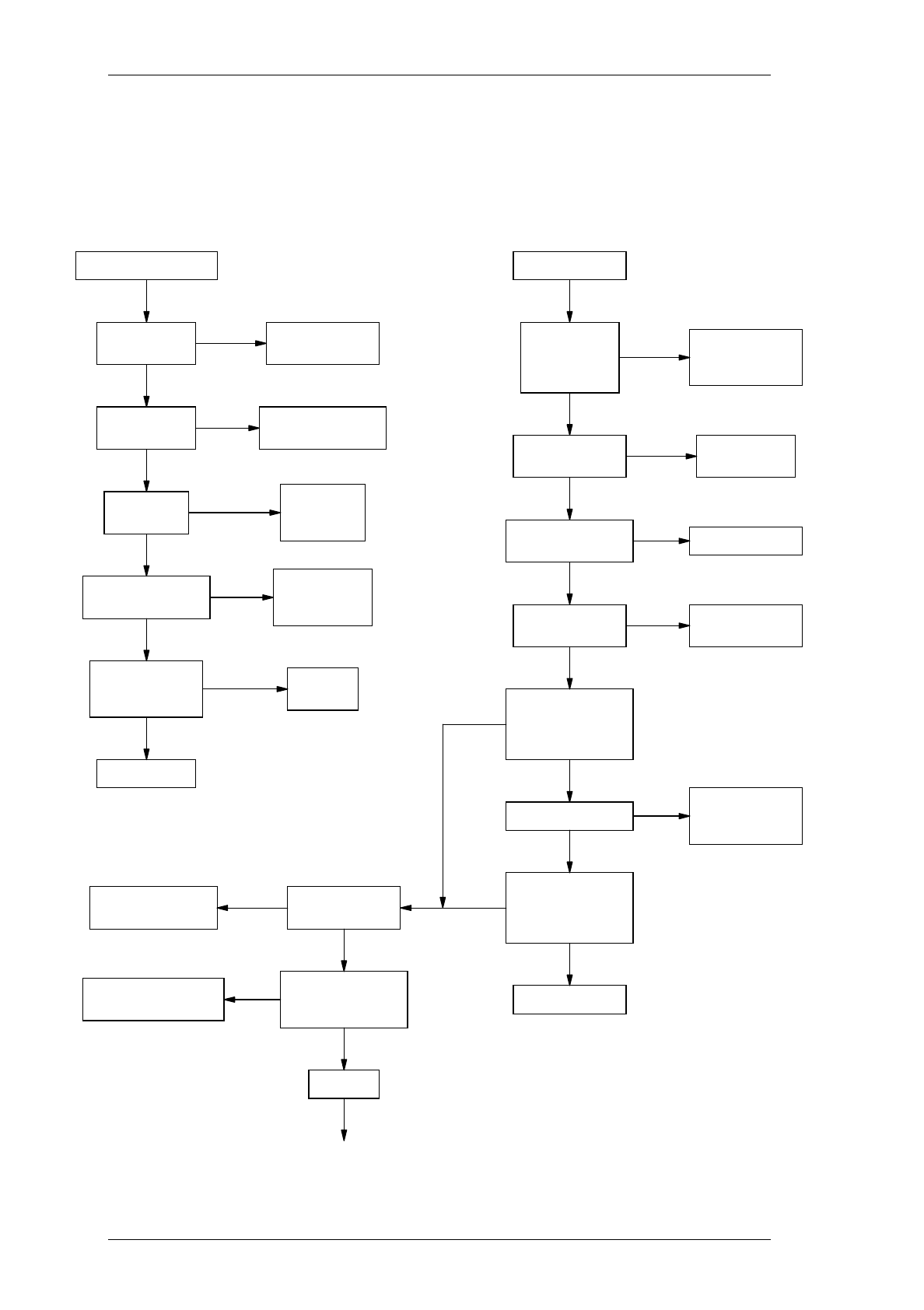
C5.12
T856/857 Fault Finding
M850-00
31/09/98 Copyright TEL
5.7.3 Synthesiser
Refer to the synthesiser circuit diagram (sheet 7) in Section 6 and the VCO circuit dia-
gram in Part E.
N
A B
Check biasin
g
resistors, Q4 & Q5.
N
Y
N
8.3V present
at VCO?
DC V present
at Q4 & Q5?
9V present at
VCO Q4/Q5?
No VCO RF output.
Y
DC V present at
VCO, Q1, Q2 & Q3?
Check biasin
g
resistors, Q1,
Q2 & Q3.
Y
N
Capacitors OK?
Check for cracks,
shorts, etc.
N
Y
Replace VCO.
Replace
if faulty.
Y
N
Y
N
N
N
Y
Y
DC V present
on Q795 emitter?
Check 9V supply.
9V present on
Q795 divider buffer?
20V inverter
supply faulty.
20V present
on IC750 pin 8?
Check 5V re
g
. &
supply resistor
to each IC.
+5V present at
IC700, IC710,
IC740, IC720
& IC730?
VCO out of lock.
Y
Y
Y
Continued on the next pa
g
e
Y
VCO freq. correct?
Synthesiser OK.
VCO trimmer
freq. ran
g
e OK?
Check VCO tunin
g
caps & trimmer.
VCO OK.
N
N
NN
N
Y
Y
Recheck
pro
g
rammin
g
via PGM800Win.
Check Q5 C
multiplier
(synth).
Check biasin
g
resistors & Q795.
Check Tx re
g
.,
Q610 & 9V re
g
.
Does VCO trimmer
adjust for stable
control line
between 3 & 16V?
Does VCO trimmer
adjust for required
frequency ran
g
e
between 3 & 16V?
Check #C1, #C7, #C8,
C6 & D1-D2 in VCO.
Is 8MHz VCO ran
g
e
achieved between
3 & 16V?

M850-00
T856/857 Fault Finding
C5.13
Copyright TEL 31/09/98
Programming and
serial bus OK?
Check programming.
Check serial bus
when programming
i.e. clock/data/enable
activity (IC740 pins
18, 19 & 17). N
Check loop filter components
R775, C774, C776, R510,
C505, IC750. Is the supply
to IC750 +20V +4, -2V?
Check regulator circuitry.
Check C772, R774, R772,
C770, R763 & Q790.
Check Q760, Q780,
R766 & C765.
Check charge pump components
(Q775 & Q780) and Q790.
Check R762 & C762.
Check the signal path from
the VCO to synthesiser.
Measure the frequency from
the VCO at IC740 pin 11 using
a frequency counter.
Is the level >-10dBm?
Does the frequency adjust
as the VCO trimmer is
adjusted (out of lock)?
Check VCO.
Y
Y
Y
Signal
Y
Y
Y
No signal
Replace synthesiser
(IC740).
Y
N Y
Y
N
N
N
N
Check phase detector output
pins (IC740 pins 3 & 4).
Are there very narrow pulses
(~50ns) at the reference frequency?
(i.e. 5kHz : 200µs period
6.25kHz : 160µs period)
*See Note below.
Is the charge pump bias
voltage at the base of
Q760 & Q780 between
3.5 and 5V? (5V when locked)
N
Is the voltage on C762,
R760, and R758 9V ±0.2V?
Is the loop filter reference
voltage at C772 (+) 6.5V ±0.2V?
N
Check divider buffer
circuit (Q795) and bias
voltages on Q795 emitter
(1.3V ±0.2V).
*Note:
When locked, both of these
are very narrow (~50ns).
If unlocked, one will be
very narrow (~50ns),
and the other wide (>15µs).
Replace synthesiser
(IC740).
Continued from previous page
B
Is the charge pump voltage
on Q790 gate between
3 and 8.5V? (6.5V ±0.2V locked)
Is reference
clock present
at IC740 pin 20
(200kHz >4.5Vpp)?
Check microcontroller
section (IC810).
N
Is reference
clock present
at IC730 pin 12
(200kHz >4.5Vpp)?
Is reference
clock present
at IC730 pin 1
(12.8MHz >4.0Vpp)?
Check TCXO (IC700)
and buffers (IC710).
N
N
Y
Y
Check phase
modulator sections:
IC720, Q710, Q720,
D710, Q730, Q740,
D720.
Check divider
IC730.
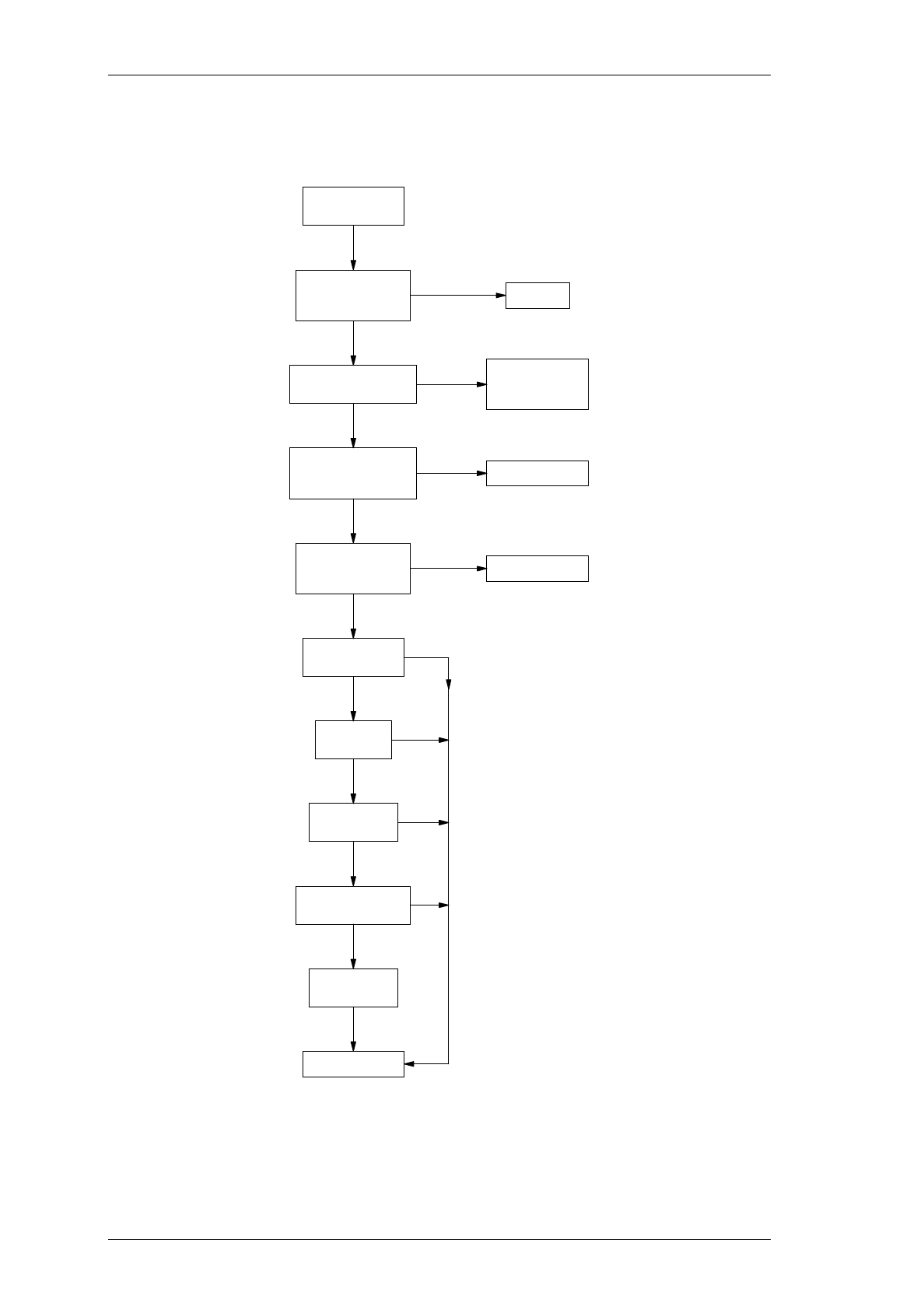
C5.14
T856/857 Fault Finding
M850-00
31/09/98 Copyright TEL
Y
N
Y
Y
Correct DC V
present on Q1 VCO?
N
Check inductors,
biasing resistors
& Q1.
Replace if faulty.
Go to B.
Loop filter &
components around
op. amp. (IC750) OK?
N
Noisy synth;
poor residual FM.
C
Isolate audio
modulation on VCO;
still noisy? Trace audio fault.
Y
Y
N
Y
Y
Y
Change trimmer;
still noisy?
Change Q1;
still noisy?
Change TCXO;
still noisy?
Change varactors;
still noisy?
Replace VCO
assembly.
Synthesiser OK.
N
N
N
N
Y
VCO phase locked?
3-16V present on
control line?
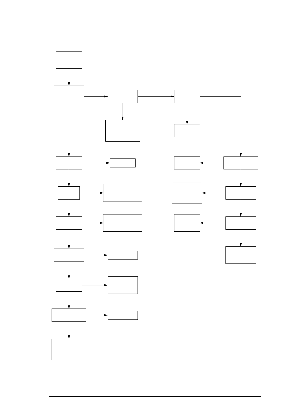
M850-00
T856/857 Fault Finding
C5.15
Copyright TEL 31/09/98
5.7.4 T856 Drive Amplifier
10.5V on Q315
collector?
Check continuity
of power rails
& DC paths to
Q365 & Q370.
Check signal
path to output
incl. output
socket (SK310).
Key exciter
& lock
synthesiser.
NN
YY
Y
Check VCO.
N
Y
Y
N
Y
Y
N
Y
N
Y
Check 9V &
13.8V supplies.
Check
regulators.
Check temp.
shutdown
circuit.
N
Y
N
Y
N
Y
10.5V on Q350
collector?
10.5V on Q355
collector?
13.8V on
IC350 pin 8?
11.5V on
IC350 pin 7?
N
Check lock det.
path back to
synth. IC740,
IC750, Q325.
Check TP305
>+8V.
Check TP320
<0.6V.
Check Q310,
Q315 circuitry
& IC350.
>2V RF at
VCO output?
>1V RF
at R381?
NCheck attenuator
pad #R517, #R518,
#R519.
>0.5V RF at
Q350 base?
Check C355, C358,
C360, Q350, D340,
D380, D360, L320.
NCheck Q350.
>1V RF at
Q355 base?
Check signal
path between
Q350 & Q355.
>6V RF at
Q355 collector? Check Q355.
>5V RF at
C362, #R395?
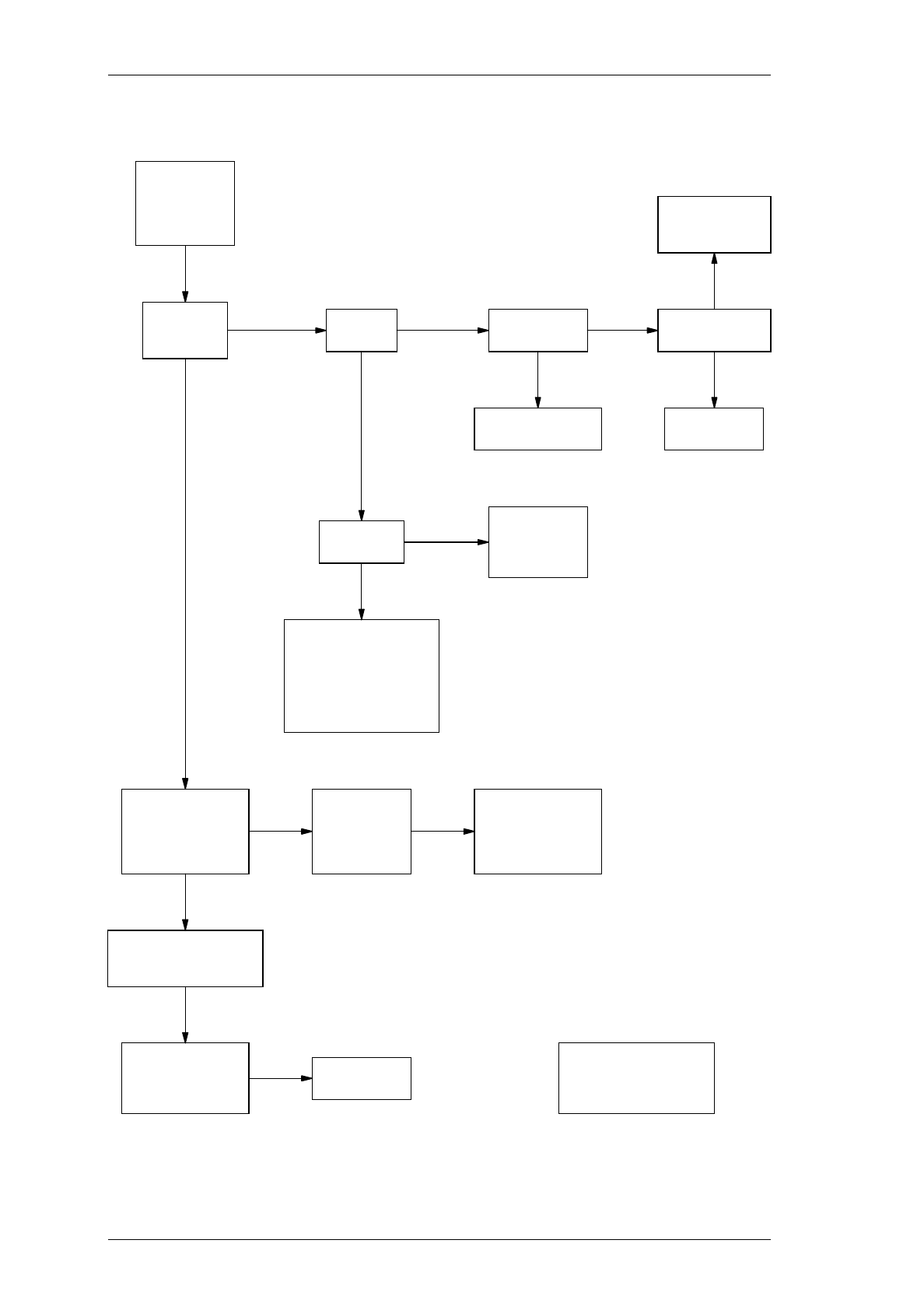
C5.16
T856/857 Fault Finding
M850-00
31/09/98 Copyright TEL
5.7.5 T856 PA & Power Control
Check IC330,
Q310, Q315
& circuitry,
+13.8V supply.
Refer to Drive Amp.
Fault Findin
g
Chart. Check supply
circuitry.
Tx deliverin
g
full power
(>30W)?
Set RV320
(power adjust)
fully clockwise;
synth. locked;
key Tx.
Y
NY
NN
Y
N
Y
N
NY
Y
Y
Y
Power control
circuitry OK.
Note:
c/w = clockwise
cc/w = counterclockwise
or anticlockwise
Check Q410,
Q420 & circuitry,
LP filter.
10.8V
at L310? Check drive at
SK310 >1.5W. Check +13.8V at
Q410 & Q420.
<2V on
IC350 pin 6?
Turn RV310 ccw.
Check power
drops to zero
slowly in a
controlled manner.
Does variation
of RV310
cause either
full power
or no power?
Check for break
in power sense
circuitry; directional
coupler D420,
D440 & circuitry.
Set RV310 so that
output power = 25W;
check L310 approx. 7.5V.
Momentarily remove
Tx load. Volta
g
e at
L310 decreases to
approx. 5V?
Check lock det. circuit;
TP305 should be >8V.
Check temp. shutdown
circuit (IC350);
TP320 should be <0.6V.
Check Q320, RV330.
Normal operating conditions:
Forward power = 4.7V approx.
Reverse power = 0.7V approx.
IC350 pin 6 = 2.02V
IC350 pin 5 = 2V
IC350 pin 7 = 8.63V

M850-00
T856/857 Fault Finding
C5.17
Copyright TEL 31/09/98
5.7.6 T857 Exciter Drive Amplifier
Check
power rails.
Check VCO.
Drive amp. OK.
N
N
Y
Y
N
Y
Y
N
Y
N
Y
9V at Q304 collector?
0.5V at Q304 base?
9V at Q305 collector?
Key exciter &
lock synthesiser.
Y
N9V at Q303
collector?
Y
>4V present on
IC300 pin 1? Check IC300.
Check Q302
& Q303.
>2V RF at
VCO output?
N
>1V RF at R323? N
Y
Check attenuator pad
R517, R518, R519.
>0.5V RF at
Q304 base?
Check C314, #C315,
#C316, Q304, L305,
D201, D202, D203.
>5V RF at
#C321, #R330?
NCheck Q304.
>1V RF at
Q305 base? Check si
g
nal path
between Q304 & Q305.
>5V RF at
Q305 collector? Check Q305.
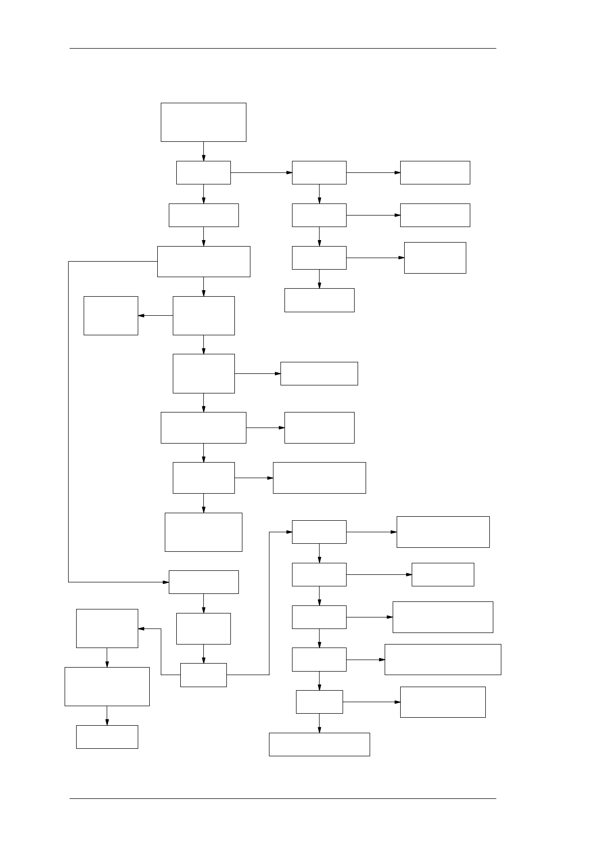
C5.18
T856/857 Fault Finding
M850-00
31/09/98 Copyright TEL
5.7.7 Audio Processor
N
IC240 pin 6
at 9V?
Key exciter &
lock synthesiser.
Connect 1kHz audio
to external CTCSS input.
Does exciter
modulate? Audio output at
IC260 pin 8?
NY
Check audio path to
VCO control line.
Check alignment
of modulators.
YN
Audio output at
IC260 pin 1?
YCheck buffer IC260
pins 8, 9 & 10.
N
Audio output at
IC260 pin 7?
Check low pass
filter stage IC260
pins 1, 2 & 3.
Y
Check stage IC260
pins 5, 6 & 7.
N
Demodulated audio
frequency response
flat between 50 & 300Hz?
Y
Check low
pass filter
stage IC260
pins 1, 2 & 3.
N
N
Y
Audio frequency
response IC260
pin 1 flat 300Hz
to 2kHz?
Audio frequency
response IC210
pin 8 6dB/octave
slope?
Check integrator
IC210 pins 8, 9, & 10.
N
Y
Audio superimposed
on 200kHz signal
IC720 pins 9 & 3 (synth)?
Check audio path
between integrator
& phase modulator.
N
Y
200kHz clipped
triangle wave at
IC720 pins 8 & 4?
Check IC720, Q710, Q720,
Q730, Q740, D710, D720,
C727, C729, C724 & C725
N
Y
Check loop filter
(IC750, pins 5, 6 & 7)
& associated
components.
Select standard
audio configuration.
Check pre-emphasis
network IC230 pins 12,
13 & 14 &/or low pass
filter IC260 pins 1, 2 & 3.
N
Y
Connect audio
to line input;
key exciter.
Does exciter
modulate?
YN
Demodulated
audio frequency
response as per
Section 4.5?
Audio processor
OK.
Audio signal at
IC210 pin 14?
Y
N
Audio signal at
IC230 pin 1?
N
Audio signal at
IC230 pin 14?
Y
N
Audio signal at
IC240 pin 4?
Y
N
Y
Check Q260 is not faulty or
being turned on inadvertently.
Y
Check audio path between
limiter IC210 pin 14 &
summing amp. IC260 pin 7.
Check IC210
pins 12, 13 & 14.
Check IC230 pins 1, 2 & 3 or
audio path between pre-
emphasis network & limiter.
Check IC230 pins 12, 13 & 14
or audio path between multiplexer
& pre-emphasis network.
Check IC240 or audio
path between line trans-
former & multiplexer.
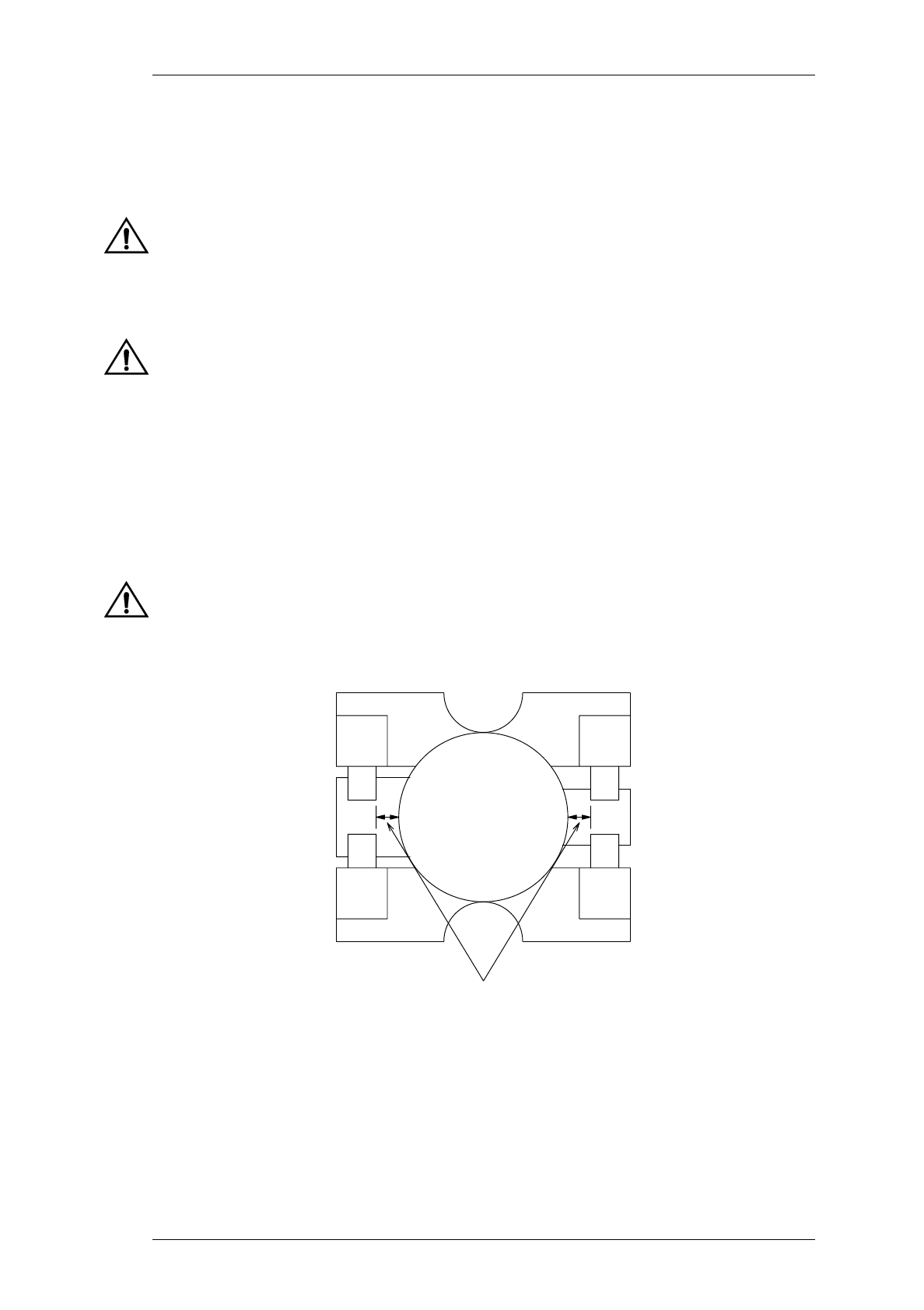
M850-00
T856/857 Fault Finding
C5.19
Copyright TEL 31/09/98
5.8 To Replace The T856 PA Transistors
(Q410 & Q420)
Caution:
Failure to comply with the following procedure can result in failure of
the device due to poor heatsinking, or worse, can endanger the health
of the assembler if the beryllium oxide die carrier is smashed during
assembly.
Caution:
As the location of certain components in the PA is critical to perform-
ance, it is important that any components removed or disturbed are
refitted in exactly the same position.
Before attempting to remove a transistor, measure the distance
between the capacitors and transistor body to the nearest 0.5mm (meas-
urement "A" in Figure 5.2) so that the capacitors can be replaced in
exactly the same position. These measurements are shown in Figure
5.2 for the 6LFL package, however the same procedure applies for the
SOE (stud) package.
Caution:
Do not apply too much heat or pressure to the PCB pads and tracks as
you may damage them or lift them from the PCB, causing permanent
damage to the transmitter.
Figure 5.2 Typical Transistor/Capacitor Spacing (Not To Scale)
Desolder and remove the components from around the transistor.
Q420 Only: Desolder and remove the two solder tags.
Desolder the transistor tabs by heating with a soldering iron and lifting away
from the PCB with a screwdriver or thin stainless steel spike, then remove the
device.
base collector
measurement A

C5.20
T856/857 Fault Finding
M850-00
31/01/99 Copyright TEL
Q410 Only: Unscrew the transistor stud nut and remove the device.
Remove any excess solder from the PCB pads with solder wick.
Trim the tabs of the replacement transistor so that the device sits neatly on the
PCB pads provided.
Lightly tin the underside of the transistor tabs.
Apply a small amount of heatsink compound (Dow-Corning 340 or equivalent) to
the transistor mounting surface. Sufficient compound should be used to ensure
an even film over the entire mounting surface.
Place the transistor on the PCB in the correct orientation and ensure the tabs are
flush to the surface.
Q410 Only: Lightly solder one tab to the PCB, then torque down the retain-
ing nut to the correct torque (0.7Nm/6in.lbf.).
Caution:
Do not solder all the tabs before torquing down otherwise the device
may be broken.
Q420 Only: Refit the solder tags.
Solder all transistor tabs to the PCB.
Replace each component in exactly the same position as noted previously.

IPN 220-01398-04
M850-00
T857 PCB Information
C6.3.29
Copyright TEL 21/06/99
T857 Parts List (IPN 220-01398-04)
How To Use This Parts List
The components listed in this parts list are divided into two main types: those with a circuit reference (e.g. C2, D1, R121, etc.) and
those without (miscellaneous and mechanical).
Those with a circuit reference are grouped in alphabetical order and then in numerical order within each group. Each component
entry comprises three or four columns: the circuit reference, variant (if applicable), IPN and description. A number in the variant col-
umn indicates that this is a variant component which is fitted only to the product type listed. Static sensitive devices are indicated by
an (S) at the start of the description column.
The miscellaneous and mechanical section lists the variant and common parts in IPN order. Where possible, a number in the legend
column indicates their position in the mechanical assembly drawing.
The Parts List Amendments box below lists component changes that took place after the parts list and diagrams in this section were
compiled. These changes (e.g. value changes, added/deleted components, etc.) are listed by circuit reference in alphanumeric order
and supersede the information given in the parts list or diagrams. Components without circuit references are listed in IPN order.
Parts List Amendments
&C289 T857-16-0500:
T857-26-0500:
T857-36-0500:
C600 Deleted
C601 Changed from 1nF (IPN 015-24100-08) to 22pF (IPN 015-22220-01)
C757 Changed from 22nF (IPN 015-25220-08) to 47nF (IPN 015-25470-08)
&R264 T857-16-0500:
T857-26-0500:
T857-36-0500:
changed from 68nF (IPN 015-25680-08) to 100nF (IPN 015-26100-08) to meet FCC Type
Approval specification (710994).
to improve cyclic keying (710980).
changed from 22k (IPN 036-15220-00) to 18k (IPN 036-15180-00) to meet FCC Type
Approval Specification (710994).

IPN 220-01398-04
C6.3.30
T857 PCB Information
M850-00
21/06/99 Copyright TEL
Ref Var IPN Description Ref Var IPN Description
C201 016-07470-06 CAP SMD ELECT BI-P 4U7 50V 20%
C202 016-07470-06 CAP SMD ELECT BI-P 4U7 50V 20%
C204 016-07470-06 CAP SMD ELECT BI-P 4U7 50V 20%
C205 016-07470-06 CAP SMD ELECT BI-P 4U7 50V 20%
C207 014-07470-00 CAP TANT CHIP 4U7 3.5 X 2.8MM
C209 015-25470-08 CAP CER 0805 47N 10% X7R 50V
C210 015-06100-08 CAP CER 1206 100N 10% X7R 50V
C211 015-06100-08 CAP CER 1206 100N 10% X7R 50V
C213 014-08100-00 CAP TANT CHIP 10M 16VW +-20%
C215 014-08220-01 (L)CAP TANT 22UF10V276MSER
C217 015-24220-08 CAP CER 0805 2N2 10% X7R 50V
C219 015-24100-08 CAP CER 0805 1N 10% X7R 50V
C221 014-08220-01 (L)CAP TANT 22UF10V276MSER
C223 015-06100-08 CAP CER 1206 100N 10% X7R 50V
C225 015-06100-08 CAP CER 1206 100N 10% X7R 50V
C227 015-06100-08 CAP CER 1206 100N 10% X7R 50V
C229 015-23150-01 CAP CER 0805 150P 5% NPO 50V
C230 015-06100-08 CAP CER 1206 100N 10% X7R 50V
C232 015-23150-01 CAP CER 0805 150P 5% NPO 50V
C233 016-08470-03 CAP SMD ELEC 47mF 20% 25v 8.3m
C235 015-24100-08 CAP CER 0805 1N 10% X7R 50V
C237 014-07100-02 CAP TANT CHIP 1U0 3.2 X 1.6MM
C239 016-07470-06 CAP SMD ELECT BI-P 4U7 50V 20%
C241 015-06100-08 CAP CER 1206 100N 10% X7R 50V
C242 014-08100-00 CAP TANT CHIP 10M 16VW +-20%
C243 015-24100-08 CAP CER 0805 1N 10% X7R 50V
C245 015-23150-01 CAP CER 0805 150P 5% NPO 50V
C247 015-23150-01 CAP CER 0805 150P 5% NPO 50V
C249 015-24100-08 CAP CER 0805 1N 10% X7R 50V
C251 015-24100-08 CAP CER 0805 1N 10% X7R 50V
C253 015-24100-08 CAP CER 0805 1N 10% X7R 50V
C255 015-24100-08 CAP CER 0805 1N 10% X7R 50V
C257 015-22470-01 CAP CER 0805 47P 5% NPO 50V
C259 015-25470-08 CAP CER 0805 47N 10% X7R 50V
C260 015-06100-08 CAP CER 1206 100N 10% X7R 50V
C261 014-07470-00 CAP TANT CHIP 4U7 3.5 X 2.8MM
C263 016-09100-05 CAP SMD ELECT 100U 25V 20%
C265 016-07470-06 CAP SMD ELECT BI-P 4U7 50V 20%
C267 015-24470-08 CAP CER 0805 4N7 10% X7R 50V
&C269 10 015-21150-01 CAP CER 0805 1P5+-1/4P NPO 50V
&C269 13 015-21150-01 CAP CER 0805 1P5+-1/4P NPO 50V
&C269 15 015-21470-01 CAP CER 0805 4P7+-1/4P NPO 50V
&C269 16 015-21470-01 CAP CER 0805 4P7+-1/4P NPO 50V
&C269 20 015-21150-01 CAP CER 0805 1P5+-1/4P NPO 50V
&C269 23 015-21150-01 CAP CER 0805 1P5+-1/4P NPO 50V
&C269 25 015-21470-01 CAP CER 0805 4P7+-1/4P NPO 50V
&C269 26 015-21470-01 CAP CER 0805 4P7+-1/4P NPO 50V
&C269 30 015-21150-01 CAP CER 0805 1P5+-1/4P NPO 50V
&C269 35 015-21470-01 CAP CER 0805 4P7+-1/4P NPO 50V
&C269 36 015-21470-01 CAP CER 0805 4P7+-1/4P NPO 50V
&C271 10 015-22470-01 CAP CER 0805 47P 5% NPO 50V
&C271 13 015-22470-01 CAP CER 0805 47P 5% NPO 50V
&C271 15 015-22470-01 CAP CER 0805 47P 5% NPO 50V
&C271 16 015-22560-01 CAP CER 0805 56P 5% NPO 50V
&C271 20 015-22470-01 CAP CER 0805 47P 5% NPO 50V
&C271 23 015-22470-01 CAP CER 0805 47P 5% NPO 50V
&C271 25 015-22470-01 CAP CER 0805 47P 5% NPO 50V
&C271 26 015-22560-01 CAP CER 0805 56P 5% NPO 50V
&C271 30 015-22470-01 CAP CER 0805 47P 5% NPO 50V
&C271 35 015-22470-01 CAP CER 0805 47P 5% NPO 50V
&C271 36 015-22560-01 CAP CER 0805 56P 5% NPO 50V
C273 015-25470-08 CAP CER 0805 47N 10% X7R 50V
C275 015-23120-01 CAP CER 0805 120P 5% NPO 50V
C277 015-25100-08 CAP CER 0805 10N 10% X7R 50V
C279 015-24100-08 CAP CER 0805 1N 10% X7R 50V
C281 015-25220-08 CAP CER 0805 22N 10% X7R 50V
C283 015-21470-01 CAP CER 0805 4P7+-1/4P NPO 50V
C285 015-21470-01 CAP CER 0805 4P7+-1/4P NPO 50V
C287 016-09100-05 CAP SMD ELECT 100U 25V 20%
&C289 10 015-25470-08 CAP CER 0805 47N 10% X7R 50V
&C289 13 015-25470-08 CAP CER 0805 47N 10% X7R 50V
&C289 15 015-25470-08 CAP CER 0805 47N 10% X7R 50V
&C289 16 015-25680-08 CAP CER 0805 68N 10% X7R 50V
&C289 20 015-25470-08 CAP CER 0805 47N 10% X7R 50V
&C289 23 015-25470-08 CAP CER 0805 47N 10% X7R 50V
&C289 25 015-25470-08 CAP CER 0805 47N 10% X7R 50V
&C289 26 015-22560-01 CAP CER 0805 56P 5% NPO 50V
&C289 30 015-25470-08 CAP CER 0805 47N 10% X7R 50V
&C289 35 015-25470-08 CAP CER 0805 47N 10% X7R 50V
&C289 36 015-25680-08 CAP CER 0805 68N 10% X7R 50V
C291 014-08220-01 (L)CAP TANT 22UF10V276MSER
C293 015-27100-10 CAP CER 0805 1M+80-20% Y5V 16V
%C294 015-22470-01 CAP CER 0805 47P 5% NPO 50V
%C295 013-06470-00 CAP SMD POLYESTER 470N 63V 10%
C300A 016-08100-01 CAP EL 6X4 10M 20% 16V
C300B 015-25100-08 CAP CER 0805 10N 10% X7R 50V
C301 015-23150-01 CAP CER 0805 150P 5% NPO 50V
C302 015-24470-08 CAP CER 0805 4N7 10% X7R 50V
C303 015-25100-08 CAP CER 0805 10N 10% X7R 50V
C304 015-24100-08 CAP CER 0805 1N 10% X7R 50V
C305 015-23100-01 CAP CER 0805 100P 5% NPO 50V
C306 015-23100-01 CAP CER 0805 100P 5% NPO 50V
C307 015-23150-01 CAP CER 0805 150P 5% NPO 50V
C308 015-23150-01 CAP CER 0805 150P 5% NPO 50V
C309 015-23150-01 CAP CER 0805 150P 5% NPO 50V
C310 015-23150-01 CAP CER 0805 150P 5% NPO 50V
C311 015-23150-01 CAP CER 0805 150P 5% NPO 50V
C312 015-23150-01 CAP CER 0805 150P 5% NPO 50V
C313 015-22220-01 CAP CER 0805 22P 5% NPO 50V
C314 015-23150-01 CAP CER 0805 150P 5% NPO 50V
#C315 10 015-22120-01 CAP CER 0805 12P 5% NPO 50V
#C315 13 015-22120-01 CAP CER 0805 12P 5% NPO 50V
#C315 15 015-22120-01 CAP CER 0805 12P 5% NPO 50V
#C315 16 015-22120-01 CAP CER 0805 12P 5% NPO 50V
#C315 20 015-21820-01 CAP CER 0805 8P2+-1/4P NPO 50V
#C315 23 015-21820-01 CAP CER 0805 8P2+-1/4P NPO 50V
#C315 25 015-21820-01 CAP CER 0805 8P2+-1/4P NPO 50V
#C315 26 015-21820-01 CAP CER 0805 8P2+-1/4P NPO 50V
#C315 30 015-21560-01 CAP CER 0805 5P6+-1/4P NPO 50V
#C315 35 015-21560-01 CAP CER 0805 5P6+-1/4P NPO 50V
#C315 36 015-21560-01 CAP CER 0805 5P6+-1/4P NPO 50V
#C316 10 015-22330-01 CAP CER 0805 33P 5% NPO 50V
#C316 13 015-22330-01 CAP CER 0805 33P 5% NPO 50V
#C316 15 015-22330-01 CAP CER 0805 33P 5% NPO 50V
#C316 16 015-22330-01 CAP CER 0805 33P 5% NPO 50V
#C316 20 015-22270-01 CAP CER 0805 27P 5% NPO 50V
#C316 23 015-22270-01 CAP CER 0805 27P 5% NPO 50V
#C316 25 015-22270-01 CAP CER 0805 27P 5% NPO 50V
#C316 26 015-22270-01 CAP CER 0805 27P 5% NPO 50V
#C316 30 015-22220-01 CAP CER 0805 22P 5% NPO 50V
#C316 35 015-22220-01 CAP CER 0805 22P 5% NPO 50V
#C316 36 015-22220-01 CAP CER 0805 22P 5% NPO 50V
C317 020-07470-04 CAP ELE RA 4M7 25V 20%8X13 SOL
C318 015-24100-08 CAP CER 0805 1N 10% X7R 50V
C319 015-24100-08 CAP CER 0805 1N 10% X7R 50V
C320 015-24100-08 CAP CER 0805 1N 10% X7R 50V
#C321 10 015-22220-01 CAP CER 0805 22P 5% NPO 50V
#C321 13 015-22220-01 CAP CER 0805 22P 5% NPO 50V
#C321 15 015-22220-01 CAP CER 0805 22P 5% NPO 50V
#C321 16 015-22220-01 CAP CER 0805 22P 5% NPO 50V
#C321 20 015-22220-01 CAP CER 0805 22P 5% NPO 50V
#C321 23 015-22220-01 CAP CER 0805 22P 5% NPO 50V
#C321 25 015-22220-01 CAP CER 0805 22P 5% NPO 50V
#C321 26 015-22220-01 CAP CER 0805 22P 5% NPO 50V
#C321 30 015-22100-01 CAP CER 0805 10P+-1/2P NPO 50V
#C321 35 015-22100-01 CAP CER 0805 10P+-1/2P NPO 50V
#C321 36 015-22100-01 CAP CER 0805 10P+-1/2P NPO 50V
#C322 10 015-21680-01 CAP CER 0805 6P8+-1/4P NPO 50V
#C322 13 015-21680-01 CAP CER 0805 6P8+-1/4P NPO 50V
#C322 15 015-21680-01 CAP CER 0805 6P8+-1/4P NPO 50V
#C322 16 015-21680-01 CAP CER 0805 6P8+-1/4P NPO 50V
#C322 20 015-22100-01 CAP CER 0805 10P+-1/2P NPO 50V
#C322 23 015-22100-01 CAP CER 0805 10P+-1/2P NPO 50V
#C322 25 015-22100-01 CAP CER 0805 10P+-1/2P NPO 50V
#C322 26 015-22100-01 CAP CER 0805 10P+-1/2P NPO 50V
#C322 30 015-21820-01 CAP CER 0805 8P2+-1/4P NPO 50V
#C322 35 015-21820-01 CAP CER 0805 8P2+-1/4P NPO 50V
#C322 36 015-21820-01 CAP CER 0805 8P2+-1/4P NPO 50V
#C323 10 015-22330-01 CAP CER 0805 33P 5% NPO 50V
#C323 13 015-22330-01 CAP CER 0805 33P 5% NPO 50V
#C323 15 015-22330-01 CAP CER 0805 33P 5% NPO 50V
#C323 16 015-22330-01 CAP CER 0805 33P 5% NPO 50V
#C323 20 015-22330-01 CAP CER 0805 33P 5% NPO 50V
#C323 23 015-22330-01 CAP CER 0805 33P 5% NPO 50V
#C323 25 015-22330-01 CAP CER 0805 33P 5% NPO 50V
#C323 26 015-22330-01 CAP CER 0805 33P 5% NPO 50V
#C323 30 015-22270-01 CAP CER 0805 27P 5% NPO 50V
#C323 35 015-22270-01 CAP CER 0805 27P 5% NPO 50V
#C323 36 015-22270-01 CAP CER 0805 27P 5% NPO 50V
C324 015-24100-08 CAP CER 0805 1N 10% X7R 50V
C325 015-06100-08 CAP CER 1206 100N 10% X7R 50V
#C326 10 015-22220-01 CAP CER 0805 22P 5% NPO 50V
#C326 13 015-22220-01 CAP CER 0805 22P 5% NPO 50V
#C326 15 015-22220-01 CAP CER 0805 22P 5% NPO 50V
#C326 16 015-22220-01 CAP CER 0805 22P 5% NPO 50V
#C326 20 015-21820-01 CAP CER 0805 8P2+-1/4P NPO 50V
#C326 23 015-21820-01 CAP CER 0805 8P2+-1/4P NPO 50V
#C326 25 015-21820-01 CAP CER 0805 8P2+-1/4P NPO 50V
#C326 26 015-21820-01 CAP CER 0805 8P2+-1/4P NPO 50V
#C326 30 015-21820-01 CAP CER 0805 8P2+-1/4P NPO 50V
#C326 35 015-21820-01 CAP CER 0805 8P2+-1/4P NPO 50V
#C326 36 015-21820-01 CAP CER 0805 8P2+-1/4P NPO 50V
#C327 10 015-21220-01 CAP CER 0805 2P2+-1/4P NPO 50V
#C327 13 015-21220-01 CAP CER 0805 2P2+-1/4P NPO 50V
#C327 15 015-21220-01 CAP CER 0805 2P2+-1/4P NPO 50V
#C327 16 015-21220-01 CAP CER 0805 2P2+-1/4P NPO 50V
#C327 20 015-21150-01 CAP CER 0805 1P5+-1/4P NPO 50V
#C327 23 015-21150-01 CAP CER 0805 1P5+-1/4P NPO 50V
#C327 25 015-21150-01 CAP CER 0805 1P5+-1/4P NPO 50V
#C327 26 015-21150-01 CAP CER 0805 1P5+-1/4P NPO 50V
#C327 30 015-21330-01 CAP CER 0805 3P3+-1/4P NPO 50V
#C327 35 015-21330-01 CAP CER 0805 3P3+-1/4P NPO 50V
#C327 36 015-21330-01 CAP CER 0805 3P3+-1/4P NPO 50V
Note: %D205 and %D210 are optional level limiting diodes for
special applications.
=R705 (47 ohm) and =SK710 are fitted in place of
=IC700 when an external frequency reference is used.
These two components are supplied with the auxiliary
D-range kits (T800-06-0000 & T800-06-0001).

IPN 220-01398-04
M850-00
T857 PCB Information
C6.3.31
Copyright TEL 21/06/99
Ref Var IPN Description Ref Var IPN Description
C328 015-23150-01 CAP CER 0805 150P 5% NPO 50V
C329 015-23150-01 CAP CER 0805 150P 5% NPO 50V
C330 015-23150-01 CAP CER 0805 150P 5% NPO 50V
C331 015-25150-08 CAP CER 0805 15N 10% X7R 50V
C332 015-06100-08 CAP CER 1206 100N 10% X7R 50V
C333 015-25100-08 CAP CER 0805 10N 10% X7R 50V
C334 015-23150-01 CAP CER 0805 150P 5% NPO 50V
C336 015-24100-08 CAP CER 0805 1N 10% X7R 50V
C337 015-23150-01 CAP CER 0805 150P 5% NPO 50V
C340 015-23150-01 CAP CER 0805 150P 5% NPO 50V
C341 015-23150-01 CAP CER 0805 150P 5% NPO 50V
C342 015-23150-01 CAP CER 0805 150P 5% NPO 50V
#C345 10 015-23120-01 CAP CER 0805 120P 5% NPO 50V
#C345 13 015-23120-01 CAP CER 0805 120P 5% NPO 50V
#C345 15 015-23120-01 CAP CER 0805 120P 5% NPO 50V
#C345 16 015-23120-01 CAP CER 0805 120P 5% NPO 50V
#C345 20 015-23120-01 CAP CER 0805 120P 5% NPO 50V
#C345 23 015-23120-01 CAP CER 0805 120P 5% NPO 50V
#C345 25 015-23120-01 CAP CER 0805 120P 5% NPO 50V
#C345 26 015-23120-01 CAP CER 0805 120P 5% NPO 50V
#C345 30 015-23120-01 CAP CER 0805 120P 5% NPO 50V
#C345 35 015-23120-01 CAP CER 0805 120P 5% NPO 50V
#C345 36 015-23120-01 CAP CER 0805 120P 5% NPO 50V
C350 015-24100-08 CAP CER 0805 1N 10% X7R 50V
C351 015-24100-08 CAP CER 0805 1N 10% X7R 50V
C354 015-23150-01 CAP CER 0805 150P 5% NPO 50V
C360 015-23120-01 CAP CER 0805 120P 5% NPO 50V
C503 015-24470-08 CAP CER 0805 4N7 10% X7R 50V
C505 015-25470-08 CAP CER 0805 47N 10% X7R 50V
C510 015-25150-08 CAP CER 0805 15N 10% X7R 50V
C513 015-25100-08 CAP CER 0805 10N 10% X7R 50V
C514 015-23150-01 CAP CER 0805 150P 5% NPO 50V
C515 015-23150-01 CAP CER 0805 150P 5% NPO 50V
C516 015-23150-01 CAP CER 0805 150P 5% NPO 50V
C535 015-06100-08 CAP CER 1206 100N 10% X7R 50V
C536 015-23100-01 CAP CER 0805 100P 5% NPO 50V
C537 015-23100-01 CAP CER 0805 100P 5% NPO 50V
C545 015-23150-01 CAP CER 0805 150P 5% NPO 50V
C546 015-23150-01 CAP CER 0805 150P 5% NPO 50V
C550 014-08220-01 (L)CAP TANT 22UF10V276MSER
C600 015-24100-08 CAP CER 0805 1N 10% X7R 50V
C601 015-24100-08 CAP CER 0805 1N 10% X7R 50V
C605 015-23120-01 CAP CER 0805 120P 5% NPO 50V
C610A 015-25100-08 CAP CER 0805 10N 10% X7R 50V
C610B 014-09100-00 CAP TANT SMD 100U 16V 20%
C611A 014-09100-00 CAP TANT SMD 100U 16V 20%
C611B 015-25100-08 CAP CER 0805 10N 10% X7R 50V
C615 015-24100-08 CAP CER 0805 1N 10% X7R 50V
C616 015-24100-08 CAP CER 0805 1N 10% X7R 50V
C623 015-23120-01 CAP CER 0805 120P 5% NPO 50V
C625 020-09470-07 CAPEL470M16V20%V 8*20 3.5L.ESR
C626 015-24470-08 CAP CER 0805 4N7 10% X7R 50V
C628 015-24100-08 CAP CER 0805 1N 10% X7R 50V
C630 015-06100-08 CAP CER 1206 100N 10% X7R 50V
C631A 015-06100-08 CAP CER 1206 100N 10% X7R 50V
C634 014-08100-00 CAP TANT CHIP 10M 16VW +-20%
C636 015-06100-08 CAP CER 1206 100N 10% X7R 50V
C638 015-23120-01 CAP CER 0805 120P 5% NPO 50V
C640 015-24100-08 CAP CER 0805 1N 10% X7R 50V
C655 015-24100-08 CAP CER 0805 1N 10% X7R 50V
C660 015-06100-08 CAP CER 1206 100N 10% X7R 50V
C665 014-08100-03 CAP TANT SMD 10U 35V 20%
C670 014-07330-10 CAP TANT SMD 3U3 35V 10%
C673 015-24470-08 CAP CER 0805 4N7 10% X7R 50V
C677 014-07100-02 CAP TANT CHIP 1U0 3.2 X 1.6MM
C681 015-06100-08 CAP CER 1206 100N 10% X7R 50V
C684 014-08100-00 CAP TANT CHIP 10M 16VW +-20%
C687 015-23120-01 CAP CER 0805 120P 5% NPO 50V
C690 015-06100-08 CAP CER 1206 100N 10% X7R 50V
C693 014-08100-00 CAP TANT CHIP 10M 16VW +-20%
C700 015-06100-08 CAP CER 1206 100N 10% X7R 50V
C703 015-24100-08 CAP CER 0805 1N 10% X7R 50V
C706 015-22470-01 CAP CER 0805 47P 5% NPO 50V
C708 014-07470-00 CAP TANT CHIP 4U7 3.5 X 2.8MM
C709 015-06100-08 CAP CER 1206 100N 10% X7R 50V
C710 015-25100-08 CAP CER 0805 10N 10% X7R 50V
C711 015-06100-08 CAP CER 1206 100N 10% X7R 50V
C712 015-22470-01 CAP CER 0805 47P 5% NPO 50V
C714 014-07470-00 CAP TANT CHIP 4U7 3.5 X 2.8MM
C719 014-07470-00 CAP TANT CHIP 4U7 3.5 X 2.8MM
C720 015-06100-08 CAP CER 1206 100N 10% X7R 50V
C722 015-06100-08 CAP CER 1206 100N 10% X7R 50V
C724 014-08220-01 (L)CAP TANT 22UF10V276MSER
C725 014-08220-01 (L)CAP TANT 22UF10V276MSER
C726 015-25100-08 CAP CER 0805 10N 10% X7R 50V
C727 015-23220-01 CAP CER 0805 220P 5% NPO 50V
C729 015-23220-01 CAP CER 0805 220P 5% NPO 50V
%C733 015-23470-08 CAP CER 0805 470P 10% X7R 50V
C735 015-22470-01 CAP CER 0805 47P 5% NPO 50V
C736 015-22470-01 CAP CER 0805 47P 5% NPO 50V
C740A 015-24100-08 CAP CER 0805 1N 10% X7R 50V
C740B 015-25100-08 CAP CER 0805 10N 10% X7R 50V
C741A 014-07470-00 CAP TANT CHIP 4U7 3.5 X 2.8MM
C741B 015-25100-08 CAP CER 0805 10N 10% X7R 50V
C742A 015-06100-08 CAP CER 1206 100N 10% X7R 50V
C742B 015-25100-08 CAP CER 0805 10N 10% X7R 50V
C743 015-22470-01 CAP CER 0805 47P 5% NPO 50V
C745 015-23120-01 CAP CER 0805 120P 5% NPO 50V
C750 014-08100-03 CAP TANT SMD 10U 35V 20%
C757 015-25220-08 CAP CER 0805 22N 10% X7R 50V
C759 015-25100-08 CAP CER 0805 10N 10% X7R 50V
C761 015-25100-08 CAP CER 0805 10N 10% X7R 50V
C762 014-08220-01 (L)CAP TANT 22UF10V276MSER
C764 015-25100-08 CAP CER 0805 10N 10% X7R 50V
C765 014-07470-00 CAP TANT CHIP 4U7 3.5 X 2.8MM
C767 015-24100-08 CAP CER 0805 1N 10% X7R 50V
C769 015-24100-08 CAP CER 0805 1N 10% X7R 50V
C770 014-08220-01 (L)CAP TANT 22UF10V276MSER
C772 014-08220-01 (L)CAP TANT 22UF10V276MSER
C774 013-06100-10 CAP SMD PPS 100N 100V 10%
C776 015-24470-08 CAP CER 0805 4N7 10% X7R 50V
C782 015-23120-01 CAP CER 0805 120P 5% NPO 50V
C784 015-23120-01 CAP CER 0805 120P 5% NPO 50V
C786 015-06100-08 CAP CER 1206 100N 10% X7R 50V
C788 015-23120-01 CAP CER 0805 120P 5% NPO 50V
C790 015-21820-01 CAP CER 0805 8P2+-1/4P NPO 50V
C792 015-23120-01 CAP CER 0805 120P 5% NPO 50V
C810 015-25470-08 CAP CER 0805 47N 10% X7R 50V
C812 015-23100-01 CAP CER 0805 100P 5% NPO 50V
C813 015-24100-08 CAP CER 0805 1N 10% X7R 50V
C822 014-07470-00 CAP TANT CHIP 4U7 3.5 X 2.8MM
C823 015-25220-08 CAP CER 0805 22N 10% X7R 50V
C824 015-25470-08 CAP CER 0805 47N 10% X7R 50V
C826 015-23220-01 CAP CER 0805 220P 5% NPO 50V
C827 015-22330-01 CAP CER 0805 33P 5% NPO 50V
C828 015-25100-08 CAP CER 0805 10N 10% X7R 50V
C830 015-25470-08 CAP CER 0805 47N 10% X7R 50V
C838 014-09100-00 CAP TANT SMD 100U 16V 20%
C841 014-09100-00 CAP TANT SMD 100U 16V 20%
C844 015-25100-08 CAP CER 0805 10N 10% X7R 50V
C910 015-01680-06 CAP CER 1210 6P8 NPO500VGRM42
C920 015-02120-06 CAP CER 1210 12P NPO500VGRM42
C930 015-01680-06 CAP CER 1210 6P8 NPO500VGRM42
D111 001-00012-90 S) DIODE MR2520L O-VOLT SUPP
D111A 001-10024-00 DIODE LDP24M 24V SUR-PROT SMD
D220 001-10000-99 S) DIODE SMD BAV99 D-SW SOT23
D230 001-10010-40 DIODE SMD ZENER 33V BZG03-C33
D240 001-10000-56 S) DIODE SMD BAW56 D-SW SOT23
D250 001-10000-56 S) DIODE SMD BAW56 D-SW SOT23
D260 001-10000-56 S) DIODE SMD BAW56 D-SW SOT23
D270 001-10000-99 S) DIODE SMD BAV99 D-SW SOT23
D301 001-10000-18 S) DIODE SMD BAT18 S-SW SOT23
D302 001-10000-18 S) DIODE SMD BAT18 S-SW SOT23
D303 001-10000-18 S) DIODE SMD BAT18 S-SW SOT23
D510 001-10000-70 S) DIODE SMD BAV70 D-SW SOT23
D610 001-10000-99 S) DIODE SMD BAV99 D-SW SOT23
D620 001-10000-70 S) DIODE SMD BAV70 D-SW SOT23
D630 001-10000-70 S) DIODE SMD BAV70 D-SW SOT23
D635 001-10065-00 DIODE SHTKY SOD123 BAT65 BAT54
D640 001-10000-70 S) DIODE SMD BAV70 D-SW SOT23
D645 001-10010-40 DIODE SMD ZENER 33V BZG03-C33
D710 001-10000-99 S) DIODE SMD BAV99 D-SW SOT23
D720 001-10000-99 S) DIODE SMD BAV99 D-SW SOT23
D730 001-10065-00 DIODE SHTKY SOD123 BAT65 BAT54
D740 001-10065-00 DIODE SHTKY SOD123 BAT65 BAT54
D810 001-10065-00 DIODE SHTKY SOD123 BAT65 BAT54
IC210 002-10003-24 S) IC SMD 324 4X O-AMP SO14
IC220 002-10126-70 S) IC SMD DS1267S10K 2XDIG POT
IC230 002-10003-24 S) IC SMD 324 4X O-AMP SO14
IC240 002-10040-53 S)MC14053B SMD BREAK B4 MAKE
IC250 002-10020-50 IC SMD 4N25A OPTOCOUPLER
IC260 002-10003-24 S) IC SMD 324 4X O-AMP SO14
IC300 002-10003-58 S) IC SMD LM358 DUAL O-AMP
IC610 002-10078-05 S) IC SMD 78L05 5V REG
IC630 002-10003-17 (S) IC LM317L REG S0-8 100MA
IC640 002-10003-58 S) IC SMD LM358 DUAL O-AMP
IC650 002-10012-32 SMD DS1232LPS-2 LP RESET&W-DOG
=IC700 539-00010-50 TCXO 12.8MHZ +-1PPM -20 +70C
IC710 002-74900-04 S) IC SMD 74HC04D 6X INV BUFFD
IC720 002-74910-04 S) IC SMD 74HCU04 6X INV
IC730 002-10045-20 S) IC SMD 74HC4520T 2XCTR 4BIT
IC740 002-14519-10 S) IC MC145191F SMD SYNTH
IC750 002-10330-78 S) IC MC33078D 2X AMP LO NOISE
IC810 002-08951-20 S) IC AT89C51 PLCC44 MIC 12MHZ
IC820 002-12416-00 S)IC SMD AT24C16N-10SC EEPROM
IC830 002-10003-24 S) IC SMD 324 4X O-AMP SO14
L300 065-10004-20 BEAD FE SMD CBD 4.6/3/3-4S2
L302 056-10330-02 (L) IND SMD 330NH
L303 065-10004-20 BEAD FE SMD CBD 4.6/3/3-4S2
L305 056-10330-02 (L) IND SMD 330NH
#L307 10 052-08130-15 COIL A/W 1.5T/3.0MM HOR 0.8MM
#L307 13 052-08130-15 COIL A/W 1.5T/3.0MM HOR 0.8MM
#L307 15 052-08130-15 COIL A/W 1.5T/3.0MM HOR 0.8MM
#L307 16 052-08130-15 COIL A/W 1.5T/3.0MM HOR 0.8MM
#L307 20 052-08130-15 COIL A/W 1.5T/3.0MM HOR 0.8MM
#L307 23 052-08130-15 COIL A/W 1.5T/3.0MM HOR 0.8MM
#L307 25 052-08130-15 COIL A/W 1.5T/3.0MM HOR 0.8MM
#L307 26 052-08130-15 COIL A/W 1.5T/3.0MM HOR 0.8MM
#L307 30 052-08120-15 COIL A/W 1.5T/2MM HOR 0.8MM
#L307 35 052-08120-15 COIL A/W 1.5T/2MM HOR 0.8MM
#L307 36 052-08120-15 COIL A/W 1.5T/2MM HOR 0.8MM
L309 065-00010-01 BEAD FERR 3B 6 HOLE
L312 052-08130-65 COIL A/W 6.5T/3.0MM HOR 0.8MM

IPN 220-01398-04
C6.3.32
T857 PCB Information
M850-00
21/06/99 Copyright TEL
Ref Var IPN Description Ref Var IPN Description
#L313 10 052-08130-15 COIL A/W 1.5T/3.0MM HOR 0.8MM
#L313 13 052-08130-15 COIL A/W 1.5T/3.0MM HOR 0.8MM
#L313 15 052-08130-15 COIL A/W 1.5T/3.0MM HOR 0.8MM
#L313 16 052-08130-15 COIL A/W 1.5T/3.0MM HOR 0.8MM
#L313 20 052-08120-15 COIL A/W 1.5T/2MM HOR 0.8MM
#L313 23 052-08120-15 COIL A/W 1.5T/2MM HOR 0.8MM
#L313 25 052-08120-15 COIL A/W 1.5T/2MM HOR 0.8MM
#L313 26 052-08120-15 COIL A/W 1.5T/2MM HOR 0.8MM
#L313 30 052-08120-15 COIL A/W 1.5T/2MM HOR 0.8MM
#L313 35 052-08120-15 COIL A/W 1.5T/2MM HOR 0.8MM
#L313 36 052-08120-15 COIL A/W 1.5T/2MM HOR 0.8MM
L314 056-10330-02 (L) IND SMD 330NH
L350 057-10120-03 IND 805 EMI SUP 120E@100M 0.2A
L535 057-10120-03 IND 805 EMI SUP 120E@100M 0.2A
L600 057-10120-03 IND 805 EMI SUP 120E@100M 0.2A
L615 057-10120-03 IND 805 EMI SUP 120E@100M 0.2A
L750 052-08125-15 COIL A/W 1.5T/2.5MM HOR 0.8MM
L910 052-08130-15 COIL A/W 1.5T/3.0MM HOR 0.8MM
L920 052-08130-15 COIL A/W 1.5T/3.0MM HOR 0.8MM
PL100 070-01001-00 D-RANGE 15 WAY COMPL T800
PL205 240-00020-67 HEADER 6W 2X3 PCB MTG STD
PL210 240-00020-67 HEADER 6W 2X3 PCB MTG STD
PL215 240-00020-44 HEADER 10W X2R PCB MTG 5*2
PL220 240-00020-67 HEADER 6W 2X3 PCB MTG STD
Q210 000-10008-48 S) XSTR SMD BCW60 NPN SOT23 SS
Q220 000-10008-17 S) XSTR SMD BC817-25 NPN SOT23
Q230 000-10008-48 S) XSTR SMD BCW60 NPN SOT23 SS
Q240 000-10008-48 S) XSTR SMD BCW60 NPN SOT23 SS
Q250 000-10008-17 S) XSTR SMD BC817-25 NPN SOT23
Q260 000-10008-57 S) XSTR SMD BCW70 PNP SOT23 SS
Q270 000-10004-10 S) XSTR SMD MJD41C NPN SW DPAK
Q301 000-10008-48 S) XSTR SMD BCW60 NPN SOT23 SS
Q302 000-10008-48 S) XSTR SMD BCW60 NPN SOT23 SS
Q304 000-00005-55 S) XSTR MRF555 NPN RF L/PWR
Q305 000-00032-56 S) XSTR MRF630 NPN T039 UHF 3W
Q306 000-10008-07 S) XSTR SMD BC807 PNP SOT23 AF
Q307 000-10008-07 S) XSTR SMD BC807 PNP SOT23 AF
Q308 000-10008-07 S) XSTR SMD BC807 PNP SOT23 AF
Q309 000-10008-57 S) XSTR SMD BCW70 PNP SOT23 SS
Q310 000-10008-48 S) XSTR SMD BCW60 NPN SOT23 SS
Q311 000-10008-48 S) XSTR SMD BCW60 NPN SOT23 SS
Q315 000-00012-15 S) XSTR BD234 PNP AF PWR TO126
Q505 000-10008-48 S) XSTR SMD BCW60 NPN SOT23 SS
Q510 000-10008-07 S) XSTR SMD BC807 PNP SOT23 AF
Q520 000-10008-07 S) XSTR SMD BC807 PNP SOT23 AF
Q530 000-10008-07 S) XSTR SMD BC807 PNP SOT23 AF
Q540 000-10008-07 S) XSTR SMD BC807 PNP SOT23 AF
Q550 000-10008-48 S) XSTR SMD BCW60 NPN SOT23 SS
Q610 000-10008-07 S) XSTR SMD BC807 PNP SOT23 AF
Q620 000-00012-15 S) XSTR BD234 PNP AF PWR TO126
Q630 000-10003-00 S) XSTR BSR30 PNP AF SOT-89
Q660 000-10008-17 S) XSTR SMD BC817-25 NPN SOT23
Q670 000-10008-57 S) XSTR SMD BCW70 PNP SOT23 SS
Q710 000-10008-48 S) XSTR SMD BCW60 NPN SOT23 SS
Q720 000-10008-57 S) XSTR SMD BCW70 PNP SOT23 SS
Q730 000-10008-48 S) XSTR SMD BCW60 NPN SOT23 SS
Q740 000-10008-57 S) XSTR SMD BCW70 PNP SOT23 SS
Q750 000-10008-07 S) XSTR SMD BC807 PNP SOT23 AF
Q760 000-10008-48 S) XSTR SMD BCW60 NPN SOT23 SS
Q770 000-10008-57 S) XSTR SMD BCW70 PNP SOT23 SS
Q775 000-10008-57 S) XSTR SMD BCW70 PNP SOT23 SS
Q780 000-10008-48 S) XSTR SMD BCW60 NPN SOT23 SS
Q785 000-10008-57 S) XSTR SMD BCW70 PNP SOT23 SS
Q790 000-10003-12 S) XSTR SMD BFR31 N JFET SOT23
Q795 000-10057-10 S) XSTR SMD BR571 NPN SOT23
Q810 000-10008-48 S) XSTR SMD BCW60 NPN SOT23 SS
Q820 000-10008-17 S) XSTR SMD BC817-25 NPN SOT23
Q830 000-10008-57 S) XSTR SMD BCW70 PNP SOT23 SS
Q840 000-10008-57 S) XSTR SMD BCW70 PNP SOT23 SS
Q850 000-10008-48 S) XSTR SMD BCW60 NPN SOT23 SS
Q860 000-10008-48 S) XSTR SMD BCW60 NPN SOT23 SS
R160 036-12100-00 RES M/F 0805 10E 5%
R201 036-13560-00 RES M/F 0805 560E 5%
R202 036-14100-00 RES M/F 0805 1K 5%
R204 036-14220-00 RES M/F 0805 2K2 5%
R205 036-13220-00 RES M/F 0805 220E 5%
R206 036-14100-00 RES M/F 0805 1K 5%
R207 036-14390-00 RES M/F 0805 3K9 5%
R208 036-13560-00 RES M/F 0805 560E 5%
R209 036-15100-00 RES M/F 0805 10K 5%
R210 036-14220-00 RES M/F 0805 2K2 5%
R211 036-13470-00 RES M/F 0805 470E 5%
R212 036-16100-00 RES M/F 0805 100K 5%
R213 036-15100-00 RES M/F 0805 10K 5%
R214 036-14820-00 RES M/F 0805 8K2 5%
R215 036-16100-00 RES M/F 0805 100K 5%
R216 036-16100-00 RES M/F 0805 100K 5%
R217 036-14100-00 RES M/F 0805 1K 5%
R218 036-16150-00 RES M/F 0805 150K 5%
R219 036-14220-00 RES M/F 0805 2K2 5%
R220 036-13470-00 RES M/F 0805 470E 5%
R221 036-14150-00 RES M/F 0805 1K5 5%
R223 036-17100-00 RES M/F 0805 1M 5%
R224 036-14680-00 RES M/F 0805 6K8 5%
R225 036-17100-00 RES M/F 0805 1M 5%
R226 036-15100-00 RES M/F 0805 10K 5%
R227 036-14220-00 RES M/F 0805 2K2 5%
R228 036-13120-00 RES M/F 0805 120E 5%
R229 036-16470-00 RES M/F 0805 470K 5%
R230 036-16100-00 RES M/F 0805 100K 5%
R231 036-15100-00 RES M/F 0805 10K 5%
R232 036-16330-00 RES M/F 0805 330K 5%
R233 036-16100-00 RES M/F 0805 100K 5%
R235 036-14470-00 RES M/F 0805 4K7 5%
R237 036-15470-00 RES M/F 0805 47K 5%
R238 036-15470-00 RES M/F 0805 47K 5%
R239 036-14150-00 RES M/F 0805 1K5 5%
R241 036-14470-00 RES M/F 0805 4K7 5%
R242 036-14220-00 RES M/F 0805 2K2 5%
R244 036-15100-00 RES M/F 0805 10K 5%
R245 036-16100-00 RES M/F 0805 100K 5%
R247 036-15100-00 RES M/F 0805 10K 5%
R248 036-16100-00 RES M/F 0805 100K 5%
R249 036-16100-00 RES M/F 0805 100K 5%
R251 036-16100-00 RES M/F 0805 100K 5%
R253 036-16100-00 RES M/F 0805 100K 5%
R254 036-16100-00 RES M/F 0805 100K 5%
R255 036-15100-00 RES M/F 0805 10K 5%
R256 036-15470-00 RES M/F 0805 47K 5%
R257 036-16330-00 RES M/F 0805 330K 5%
R258 036-16150-00 RES M/F 0805 150K 5%
R259 036-15220-00 RES M/F 0805 22K 5%
R260 036-15470-00 RES M/F 0805 47K 5%
R262 036-15470-00 RES M/F 0805 47K 5%
R263 036-14470-00 RES M/F 0805 4K7 5%
&R264 10 036-15220-00 RES M/F 0805 22K 5%
&R264 13 036-15220-00 RES M/F 0805 22K 5%
&R264 15 036-15270-10 RES M/F 0805 27K 1%
&R264 16 036-15220-00 RES M/F 0805 22K 5%
&R264 20 036-15220-00 RES M/F 0805 22K 5%
&R264 23 036-15220-00 RES M/F 0805 22K 5%
&R264 25 036-15270-10 RES M/F 0805 27K 1%
&R264 26 036-15220-00 RES M/F 0805 22K 5%
&R264 30 036-15220-00 RES M/F 0805 22K 5%
&R264 35 036-15270-10 RES M/F 0805 27K 1%
&R264 36 036-15220-00 RES M/F 0805 22K 5%
&R265 10 036-15150-00 RES M/F 0805 15K 5%
&R265 13 036-15150-00 RES M/F 0805 15K 5%
&R265 15 036-15180-10 RES M/F 0805 18K 1%
&R265 16 036-15150-00 RES M/F 0805 15K 5%
&R265 20 036-15150-00 RES M/F 0805 15K 5%
&R265 23 036-15150-00 RES M/F 0805 15K 5%
&R265 25 036-15180-10 RES M/F 0805 18K 1%
&R265 26 036-15150-00 RES M/F 0805 15K 5%
&R265 30 036-15150-00 RES M/F 0805 15K 5%
&R265 35 036-15180-10 RES M/F 0805 18K 1%
&R265 36 036-15150-00 RES M/F 0805 15K 5%
&R266 10 036-15470-10 RES M/F 0805 47K 1%
&R266 13 036-15470-10 RES M/F 0805 47K 1%
&R266 15 036-15560-00 RES M/F 0805 56K 5%
&R266 16 036-15470-10 RES M/F 0805 47K 1%
&R266 20 036-15470-00 RES M/F 0805 47K 5%
&R266 23 036-15470-10 RES M/F 0805 47K 1%
&R266 25 036-15560-00 RES M/F 0805 56K 5%
&R266 26 036-15470-10 RES M/F 0805 47K 1%
&R266 30 036-15470-10 RES M/F 0805 47K 1%
&R266 35 036-15560-00 RES M/F 0805 56K 5%
&R266 36 036-15470-10 RES M/F 0805 47K 1%
R267 036-14220-00 RES M/F 0805 2K2 5%
R268 036-13100-00 RES M/F 0805 100E 5%
R269 036-15100-00 RES M/F 0805 10K 5%
R270 036-14120-00 RES M/F 0805 1K2 5%
R271 036-17100-00 RES M/F 0805 1M 5%
R272 036-13560-00 RES M/F 0805 560E 5%
R273 036-15120-00 RES M/F 0805 12K 5%
R274 036-15150-00 RES M/F 0805 15K 5%
R275 036-14270-00 RES M/F 0805 2K7 5%
R277 036-16100-00 RES M/F 0805 100K 5%
R278 036-16120-00 RES M/F 0805 120K 5%
R279 036-17100-00 RES M/F 0805 1M 5%
R280 036-15100-00 RES M/F 0805 10K 5%
R282 036-15560-00 RES M/F 0805 56K 5%
R283 036-15560-00 RES M/F 0805 56K 5%
R284 036-17100-00 RES M/F 0805 1M 5%
R285 036-10000-00 RES M/F 0805 ZERO OHM
R286 036-14220-00 RES M/F 0805 2K2 5%
R287 036-15100-00 RES M/F 0805 10K 5%
R288 036-15120-00 RES M/F 0805 12K 5%
R289 036-16100-00 RES M/F 0805 100K 5%
&R290 10 036-13560-00 RES M/F 0805 560E 5%
&R290 13 036-13560-00 RES M/F 0805 560E 5%
&R290 15 036-13560-00 RES M/F 0805 560E 5%
&R290 16 036-13680-00 RES M/F 0805 680E 5%
&R290 20 036-13560-00 RES M/F 0805 560E 5%
&R290 23 036-13560-00 RES M/F 0805 560E 5%
&R290 25 036-13560-00 RES M/F 0805 560E 5%
&R290 26 036-13680-00 RES M/F 0805 680E 5%
&R290 30 036-13560-00 RES M/F 0805 560E 5%
&R290 35 036-13560-00 RES M/F 0805 560E 5%
&R290 36 036-13680-00 RES M/F 0805 680E 5%
R291 036-10000-00 RES M/F 0805 ZERO OHM
R292 036-14470-00 RES M/F 0805 4K7 5%
R293 036-15470-00 RES M/F 0805 47K 5%

IPN 220-01398-04
M850-00
T857 PCB Information
C6.3.33
Copyright TEL 21/06/99
Ref Var IPN Description Ref Var IPN Description
R294 036-14470-00 RES M/F 0805 4K7 5%
R295 036-14270-00 RES M/F 0805 2K7 5%
R296 036-14100-00 RES M/F 0805 1K 5%
R297 036-14560-00 RES M/F 0805 5K6 5%
%R298 036-16100-00 RES M/F 0805 100K 5%
R299 036-14270-00 RES M/F 0805 2K7 5%
R300 036-12220-00 RES M/F 0805 22E 5%
R301 036-15100-00 RES M/F 0805 10K 5%
R302 036-15220-00 RES M/F 0805 22K 5%
R303 036-14270-00 RES M/F 0805 2K7 5%
R304 036-16100-00 RES M/F 0805 100K 5%
R305 036-15220-00 RES M/F 0805 22K 5%
#R306 10 036-14150-00 RES M/F 0805 1K5 5%
#R306 13 036-14150-00 RES M/F 0805 1K5 5%
#R306 15 036-14150-00 RES M/F 0805 1K5 5%
#R306 16 036-14150-00 RES M/F 0805 1K5 5%
#R306 20 036-14220-00 RES M/F 0805 2K2 5%
#R306 23 036-14220-00 RES M/F 0805 2K2 5%
#R306 25 036-14220-00 RES M/F 0805 2K2 5%
#R306 26 036-14220-00 RES M/F 0805 2K2 5%
#R306 30 036-14150-00 RES M/F 0805 1K5 5%
#R306 35 036-14150-00 RES M/F 0805 1K5 5%
#R306 36 036-14150-00 RES M/F 0805 1K5 5%
#R307 10 036-13470-00 RES M/F 0805 470E 5%
#R307 13 036-13470-00 RES M/F 0805 470E 5%
#R307 15 036-13470-00 RES M/F 0805 470E 5%
#R307 16 036-13470-00 RES M/F 0805 470E 5%
#R307 20 036-13150-00 RES M/F 0805 150E 5%
#R307 23 036-13150-00 RES M/F 0805 150E 5%
#R307 25 036-13150-00 RES M/F 0805 150E 5%
#R307 26 036-13150-00 RES M/F 0805 150E 5%
#R307 30 036-13470-00 RES M/F 0805 470E 5%
#R307 35 036-13470-00 RES M/F 0805 470E 5%
#R307 36 036-13470-00 RES M/F 0805 470E 5%
R308 036-14220-00 RES M/F 0805 2K2 5%
R309 036-15100-00 RES M/F 0805 10K 5%
R310 036-13470-00 RES M/F 0805 470E 5%
R311 036-13470-00 RES M/F 0805 470E 5%
R312 036-14100-00 RES M/F 0805 1K 5%
R313 036-12220-00 RES M/F 0805 22E 5%
R314 036-13470-00 RES M/F 0805 470E 5%
R315 036-03110-10 RES 10R 1W SMD 2512
R322 036-12100-00 RES M/F 0805 10E 5%
R323 036-14150-00 RES M/F 0805 1K5 5%
R324 036-12470-00 RES M/F 0805 47E 5%
R325 036-13560-00 RES M/F 0805 560E 5%
R326 036-12470-00 RES M/F 0805 47E 5%
R327 036-14100-00 RES M/F 0805 1K 5%
R328 036-13470-00 RES M/F 0805 470E 5%
R329 036-12100-00 RES M/F 0805 10E 5%
#R330 10 030-53470-20 RES FILM AI 470E 5% 0.4W 4X1.6
#R330 13 030-53470-20 RES FILM AI 470E 5% 0.4W 4X1.6
#R330 15 030-53470-20 RES FILM AI 470E 5% 0.4W 4X1.6
#R330 16 030-53470-20 RES FILM AI 470E 5% 0.4W 4X1.6
#R330 20 030-53470-20 RES FILM AI 470E 5% 0.4W 4X1.6
#R330 23 030-53470-20 RES FILM AI 470E 5% 0.4W 4X1.6
#R330 25 030-53470-20 RES FILM AI 470E 5% 0.4W 4X1.6
#R330 26 030-53470-20 RES FILM AI 470E 5% 0.4W 4X1.6
#R330 30 030-53220-20 RES FILM AI 220E 5% 0.4W 4X1.6
#R330 35 030-53220-20 RES FILM AI 220E 5% 0.4W 4X1.6
#R330 36 030-53220-20 RES FILM AI 220E 5% 0.4W 4X1.6
#R331 10 030-52120-20 RES M/F 12E 5% 4X1.6 0.2"
#R331 13 030-52120-20 RES M/F 12E 5% 4X1.6 0.2"
#R331 15 030-52120-20 RES M/F 12E 5% 4X1.6 0.2"
#R331 16 030-52120-20 RES M/F 12E 5% 4X1.6 0.2"
#R331 20 030-52120-20 RES M/F 12E 5% 4X1.6 0.2"
#R331 23 030-52120-20 RES M/F 12E 5% 4X1.6 0.2"
#R331 25 030-52120-20 RES M/F 12E 5% 4X1.6 0.2"
#R331 26 030-52120-20 RES M/F 12E 5% 4X1.6 0.2"
#R331 30 030-52220-20 RES FILM AI 22E 5% 0.4W 4X1.6
#R331 35 030-52220-20 RES FILM AI 22E 5% 0.4W 4X1.6
#R331 36 030-52220-20 RES FILM AI 22E 5% 0.4W 4X1.6
#R332 10 030-53470-20 RES FILM AI 470E 5% 0.4W 4X1.6
#R332 13 030-53470-20 RES FILM AI 470E 5% 0.4W 4X1.6
#R332 15 030-53470-20 RES FILM AI 470E 5% 0.4W 4X1.6
#R332 16 030-53470-20 RES FILM AI 470E 5% 0.4W 4X1.6
#R332 20 030-53470-20 RES FILM AI 470E 5% 0.4W 4X1.6
#R332 23 030-53470-20 RES FILM AI 470E 5% 0.4W 4X1.6
#R332 25 030-53470-20 RES FILM AI 470E 5% 0.4W 4X1.6
#R332 26 030-53470-20 RES FILM AI 470E 5% 0.4W 4X1.6
#R332 30 030-53220-20 RES FILM AI 220E 5% 0.4W 4X1.6
#R332 35 030-53220-20 RES FILM AI 220E 5% 0.4W 4X1.6
#R332 36 030-53220-20 RES FILM AI 220E 5% 0.4W 4X1.6
R333 036-12470-00 RES M/F 0805 47E 5%
R334 032-33100-10 RES M/F PWR 100E 5% 2W 12X4.5
R335 036-12100-00 RES M/F 0805 10E 5%
R336 036-16150-00 RES M/F 0805 150K 5%
R337 036-16150-00 RES M/F 0805 150K 5%
R338 036-16150-00 RES M/F 0805 150K 5%
R339 036-16150-00 RES M/F 0805 150K 5%
R340 036-14150-00 RES M/F 0805 1K5 5%
R341 036-15100-00 RES M/F 0805 10K 5%
R342 036-15100-00 RES M/F 0805 10K 5%
R343 036-15150-00 RES M/F 0805 15K 5%
R344 036-15470-00 RES M/F 0805 47K 5%
R345 036-16120-00 RES M/F 0805 120K 5%
R346 036-15100-00 RES M/F 0805 10K 5%
R347 036-14100-00 RES M/F 0805 1K 5%
R348 036-14100-00 RES M/F 0805 1K 5%
R349 036-16100-00 RES M/F 0805 100K 5%
R350 036-12220-00 RES M/F 0805 22E 5%
R355 036-14100-00 RES M/F 0805 1K 5%
R356 036-15150-00 RES M/F 0805 15K 5%
R357 036-15150-00 RES M/F 0805 15K 5%
R358 036-14470-00 RES M/F 0805 4K7 5%
R359 036-14100-00 RES M/F 0805 1K 5%
R501 036-15100-00 RES M/F 0805 10K 5%
R502 036-15100-00 RES M/F 0805 10K 5%
R503 036-14560-00 RES M/F 0805 5K6 5%
R504 036-13330-00 RES M/F 0805 330E 5%
R505 036-15150-00 RES M/F 0805 15K 5%
R510 036-14150-00 RES M/F 0805 1K5 5%
R514 036-12330-00 RES M/F 0805 33E 5%
R515 036-12560-00 RES M/F 0805 56E 5%
R517 036-13330-00 RES M/F 0805 330E 5%
R518 036-12180-00 RES M/F 0805 18E 5%
R519 036-13330-00 RES M/F 0805 330E 5%
R520 036-16120-00 RES M/F 0805 120K 5%
R525 036-15470-00 RES M/F 0805 47K 5%
R530 036-15220-00 RES M/F 0805 22K 5%
R535 036-15100-00 RES M/F 0805 10K 5%
R540 036-14220-00 RES M/F 0805 2K2 5%
R545 036-14470-00 RES M/F 0805 4K7 5%
%R550 036-14470-00 RES M/F 0805 4K7 5%
R555 036-14470-00 RES M/F 0805 4K7 5%
R560 036-13470-00 RES M/F 0805 470E 5%
R609 036-14100-00 RES M/F 0805 1K 5%
R613 036-13560-00 RES M/F 0805 560E 5%
R615 036-13100-00 RES M/F 0805 100E 5%
R617 036-10000-00 RES M/F 0805 ZERO OHM
R619 036-01100-10 RES 1 OHM 1 WATT 2512 CHIP
R621 036-01100-10 RES 1 OHM 1 WATT 2512 CHIP
R625 036-14100-00 RES M/F 0805 1K 5%
R629 036-03270-10 RES 270 OHM 1 WATT 2512 CHIP
R633 036-14680-00 RES M/F 0805 6K8 5%
R637 036-12220-00 RES M/F 0805 22E 5%
R638 036-12220-00 RES M/F 0805 22E 5%
R640 036-12100-00 RES M/F 0805 10E 5%
R641 036-14150-00 RES M/F 0805 1K5 5%
R645 036-13470-00 RES M/F 0805 470E 5%
R649 036-14470-00 RES M/F 0805 4K7 5%
R653 036-15100-00 RES M/F 0805 10K 5%
R655 036-10000-00 RES M/F 0805 ZERO OHM
R656 036-10000-00 RES M/F 0805 ZERO OHM
R657 036-15100-00 RES M/F 0805 10K 5%
R661 036-15100-00 RES M/F 0805 10K 5%
R665 036-16100-00 RES M/F 0805 100K 5%
R669 036-15470-00 RES M/F 0805 47K 5%
R673 036-16100-00 RES M/F 0805 100K 5%
R677 036-15470-00 RES M/F 0805 47K 5%
R681 036-13100-00 RES M/F 0805 100E 5%
R685 036-15150-00 RES M/F 0805 15K 5%
R689 036-12100-00 RES M/F 0805 10E 5%
R693 036-16100-00 RES M/F 0805 100K 5%
R696 036-15560-00 RES M/F 0805 56K 5%
R701 036-12220-00 RES M/F 0805 22E 5%
R702 036-17100-00 RES M/F 0805 1M 5%
R703 036-17100-00 RES M/F 0805 1M 5%
R704 036-15180-00 RES M/F 0805 18K 5%
R706 036-12100-00 RES M/F 0805 10E 5%
R708 036-17100-00 RES M/F 0805 1M 5%
R710 036-13100-00 RES M/F 0805 100E 5%
R711 036-13100-00 RES M/F 0805 100E 5%
R712 036-12100-00 RES M/F 0805 10E 5%
R713 036-10000-00 RES M/F 0805 ZERO OHM
R714 036-12100-00 RES M/F 0805 10E 5%
%R715 036-14100-00 RES M/F 0805 1K 5%
R717 036-14270-00 RES M/F 0805 2K7 5%
R718 036-16150-00 RES M/F 0805 150K 5%
R719 036-16150-00 RES M/F 0805 150K 5%
R720 036-15390-00 RES M/F 0805 39K 5%
R721 036-15100-00 RES M/F 0805 10K 5%
R722 036-15100-00 RES M/F 0805 10K 5%
R723 036-14270-00 RES M/F 0805 2K7 5%
R725 036-15390-00 RES M/F 0805 39K 5%
%R726 036-13100-00 RES M/F 0805 100E 5%
R727 036-15100-00 RES M/F 0805 10K 5%
R728 036-15100-00 RES M/F 0805 10K 5%
R734 036-13470-00 RES M/F 0805 470E 5%
R735 036-13470-00 RES M/F 0805 470E 5%
R736 036-13470-00 RES M/F 0805 470E 5%
R742 036-13150-00 RES M/F 0805 150E 5%
R743 036-13150-00 RES M/F 0805 150E 5%
R744 036-12220-00 RES M/F 0805 22E 5%
R746 036-12220-00 RES M/F 0805 22E 5%
R747 036-12220-00 RES M/F 0805 22E 5%
R748 036-15470-00 RES M/F 0805 47K 5%
R749 036-15470-00 RES M/F 0805 47K 5%
R750 036-12220-00 RES M/F 0805 22E 5%
R752 036-12220-00 RES M/F 0805 22E 5%
R753 036-17100-00 RES M/F 0805 1M 5%
R754 036-14100-00 RES M/F 0805 1K 5%
R756 036-15120-00 RES M/F 0805 12K 5%
R757 036-15120-00 RES M/F 0805 12K 5%
R758 036-14120-00 RES M/F 0805 1K2 5%
R759 036-13330-00 RES M/F 0805 330E 5%

IPN 220-01398-04
C6.3.34
T857 PCB Information
M850-00
21/06/99 Copyright TEL
Ref Var IPN Description Ref Var IPN Description
R760 036-13180-00 RES M/F 0805 180E 5%
R762 036-13100-00 RES M/F 0805 100E 5%
R763 036-13100-00 RES M/F 0805 100E 5%
R765 036-13680-00 RES M/F 0805 680E 5%
R766 036-14100-00 RES M/F 0805 1K 5%
R767 036-13680-00 RES M/F 0805 680E 5%
R769 036-13180-00 RES M/F 0805 180E 5%
R771 036-14820-00 RES M/F 0805 8K2 5%
R772 036-15220-00 RES M/F 0805 22K 5%
R774 036-14820-00 RES M/F 0805 8K2 5%
R775 036-15180-00 RES M/F 0805 18K 5%
R777 036-14220-00 RES M/F 0805 2K2 5%
R780 036-12680-00 RES M/F 0805 68E 5%
R782 036-12180-00 RES M/F 0805 18E 5%
R784 036-13120-00 RES M/F 0805 120E 5%
R785 036-14330-00 RES M/F 0805 3K3 5%
R786 036-12100-00 RES M/F 0805 10E 5%
R787 036-12100-00 RES M/F 0805 10E 5%
R790 036-13390-00 RES M/F 0805 390E 5%
R791 036-14100-00 RES M/F 0805 1K 5%
R801 036-16150-00 RES M/F 0805 150K 5%
R802 036-15470-00 RES M/F 0805 47K 5%
R808 036-12100-00 RES M/F 0805 10E 5%
R809 036-14470-00 RES M/F 0805 4K7 5%
R810 036-14470-00 RES M/F 0805 4K7 5%
R811 036-14470-00 RES M/F 0805 4K7 5%
R812 036-14470-00 RES M/F 0805 4K7 5%
R813 036-14470-00 RES M/F 0805 4K7 5%
R815 036-15470-00 RES M/F 0805 47K 5%
R816 036-16150-00 RES M/F 0805 150K 5%
R818 036-14470-00 RES M/F 0805 4K7 5%
R819 036-14470-00 RES M/F 0805 4K7 5%
R821 036-15470-00 RES M/F 0805 47K 5%
R822 036-15470-00 RES M/F 0805 47K 5%
R824 036-14220-00 RES M/F 0805 2K2 5%
R825 036-14220-00 RES M/F 0805 2K2 5%
R826 036-14220-00 RES M/F 0805 2K2 5%
R827 036-14220-00 RES M/F 0805 2K2 5%
R828 036-14220-00 RES M/F 0805 2K2 5%
R829 036-14220-00 RES M/F 0805 2K2 5%
R830 036-14220-00 RES M/F 0805 2K2 5%
R831 036-14220-00 RES M/F 0805 2K2 5%
R832 036-14220-00 RES M/F 0805 2K2 5%
R833 036-14220-00 RES M/F 0805 2K2 5%
R835 036-14220-00 RES M/F 0805 2K2 5%
R836 036-14220-00 RES M/F 0805 2K2 5%
R837 036-14220-00 RES M/F 0805 2K2 5%
R840 036-14220-00 RES M/F 0805 2K2 5%
R841 036-14220-00 RES M/F 0805 2K2 5%
R842 036-14220-00 RES M/F 0805 2K2 5%
R843 036-14220-00 RES M/F 0805 2K2 5%
R845 036-13470-00 RES M/F 0805 470E 5%
R847 036-13470-00 RES M/F 0805 470E 5%
R848 036-14470-00 RES M/F 0805 4K7 5%
R849 036-13470-00 RES M/F 0805 470E 5%
R850 036-13470-00 RES M/F 0805 470E 5%
R853 036-14470-00 RES M/F 0805 4K7 5%
R854 036-14470-00 RES M/F 0805 4K7 5%
R855 036-14470-00 RES M/F 0805 4K7 5%
R859 036-16150-00 RES M/F 0805 150K 5%
R861 036-16150-00 RES M/F 0805 150K 5%
R863 036-16150-00 RES M/F 0805 150K 5%
R865 036-16100-00 RES M/F 0805 100K 5%
R867 036-16100-00 RES M/F 0805 100K 5%
R871 036-15470-00 RES M/F 0805 47K 5%
R872 036-14470-00 RES M/F 0805 4K7 5%
R873 036-15330-00 RES M/F 0805 33K 5%
R874 036-14470-00 RES M/F 0805 4K7 5%
R875 036-15470-00 RES M/F 0805 47K 5%
R876 036-14470-00 RES M/F 0805 4K7 5%
R877 036-14470-00 RES M/F 0805 4K7 5%
R879 036-15100-00 RES M/F 0805 10K 5%
RV210 040-05100-23 POT 10K LOG PCB 15MM SLOT SFT
RV220 042-05500-05 RES PRESET SMD 50K CER 4MM SQ
RV805 042-05200-05 RES PRESET SMD 20K CER 4MM SQ
SK200 240-10000-05 CONN SMD SKT 8W 2R M-MATCH
SK205 240-02020-05 SKT STEREO PHONE JACK PCB MTG
SK310 240-02100-44 SKT COAX MINI JACK PCB MT ANG.
SK410 240-02100-44 SKT COAX MINI JACK PCB MT ANG.
SK501 240-04021-77 SKT JACK 1.3 PCB MT 64W
SK502 240-04021-77 SKT JACK 1.3 PCB MT 64W
SK503 240-04021-77 SKT JACK 1.3 PCB MT 64W
SK504 240-04021-77 SKT JACK 1.3 PCB MT 64W
SK505 240-04021-77 SKT JACK 1.3 PCB MT 64W
SK513 240-04021-77 SKT JACK 1.3 PCB MT 64W
SK522 240-04021-77 SKT JACK 1.3 PCB MT 64W
SK531 240-04021-77 SKT JACK 1.3 PCB MT 64W
SK532 240-04021-77 SKT JACK 1.3 PCB MT 64W
SK533 240-04021-77 SKT JACK 1.3 PCB MT 64W
SK534 240-04021-77 SKT JACK 1.3 PCB MT 64W
SK535 240-04021-77 SKT JACK 1.3 PCB MT 64W
SK805 240-10000-07 CONN SMD SKT 16W 2R M-MATCH
SK810 240-04020-42 SKT 44 PIN SMD PLCC
SW230 232-00010-26 SWITCH PUSH SPDT R-ANG PCB MTG
T210 053-00010-17 XFMR T4030 LINE MATCH POTCORE
T610 050-00016-50 COIL TAIT NO 650 455KHZ

IPN 220-01398-04
M850-00
T857 PCB Information
C6.3.35
Copyright TEL 21/06/99

IPN 220-01398-04
C6.3.36
T857 PCB Information
M850-00
21/06/99 Copyright TEL
IPN Legend Description IPN Legend Description
T857 Mechanical & Miscellaneous Parts (220-01398-04)
008-00014-79 S)LED 3MM RED WITH WIRE
008-00014-80 S)LED 3MM GREEN WITH WIRE
070-01001-00 1 D-RANGE 15 WAY COMPL T800
219-02610-00 COAX 220MM 2 MINI PIN CRIMP
Connects SK310 to SK410.
220-01145-02 2 PCB T85X VCO
220-01398-04 3 PCB T857 SERIES II TOP
232-00020-26 4 BUTTON 232-00010-26 SWITCH
240-02100-06 5 SKT COAX N TYPE PNL MTG OP-TER
240-04020-62 SKT 2 W RECEP SHORTING LINK
PL205/210/215/220.
303-11169-04 6 CHASSIS PAINTED T800 SERIES
303-23118-00 7 COVER A3M2247 D RANGE T855/7
303-50074-00 8 CLIP A3M2246 SPRING CLAMP T857
303-50078-00 9 CLIP A4M2630 SPR. CABLE CLAMP
308-01007-01 10 HANDLE BASE STATION SERIES II
312-01052-02 11 LID TOP T800 SER II PTND
312-01053-02 12 LID BOTTOM T800 SER II PNTD
316-06619-00 13 PNL FRT EX, NO EX OUT SER II
345-00040-10 14 SCRW M3X6MM P/POZ ST BZ
349-00020-36 15 LIM)SCREW TT M3X8m PANTORX BLK
349-00020-43 16 SCRW T/T M4X12MM P/POZ BZ
349-00020-45 17 SCRW T/T M4X20MM P/POZ BZ
350-00016-42 18 SPACER 5MM HI 8MM ST 2.5MM HO
352-00010-08 19 NUT M3 COLD FORM HEX ST BZ
352-00010-29 20 NUT M4 NYLOC HEX
353-00010-10 21 WSHR M3 FLAT 7MMX0.6MM ST BZ
353-00010-13 22 WSHR M3 S/PROOF INT BZ
353-00010-24 23 WSHR M4X8MM FLAT
362-00010-23 24 GASKET SIL TO-220 CLIP MTG.
362-00010-33 25 GROMMET LED MTG 3MM
365-00011-53 LABEL 104X37MM
365-00100-20 LABEL WHITE S/A 28X11MM
365-01541-00 LABEL TX/RX/EX TYPE APR/SER NO
399-00010-51 BAG PLASTIC 75X100MM
410-01081-01 CRT T800 SERIES II
410-01082-01 CRTN 10 T800 KIWI 423X410X360

IPN 220-01398-04
M850-00
T857 PCB Information
C6.3.37
Copyright TEL 21/06/99
replace A4 pages C6.3.37/C6.3.38 with A3 pages C6.3.37/C6.3.38

IPN 220-01398-04
C6.3.38
T857 PCB Information
M850-00
21/06/99 Copyright TEL
replace A4 pages C6.3.37/C6.3.38 with A3 pages C6.3.37/C6.3.38

IPN 220-01398-04
M850-00
T857 PCB Information
C6.3.39
Copyright TEL 21/06/99
Device PCB Circuit Device PCB CircuitDevice PCB Circuit Device PCB Circuit
T857 Grid Reference Index (IPN 220-01398-04)
How To Use This Grid Reference Index
The first digit in the PCB layout reference is a "1" or "2", indicating the top or bottom side layout respectively, and the last two charac-
ters give the location of the component on that diagram.
The first digit in the circuit diagram reference is the sheet number, and the last two characters give the location of the component on
that sheet.
C201 1:C1 2-B8
C202 1:C1 2-C8
C204 1:B3 2-E8
C205 1:A3 2-E8
C207 1:C7 2-B6
C209 1:C6 2-D6
C210 1:C7 2-K0
C211 1:B7 2-F8
C213 1:B6 2-G8
C215 1:B6 2-G8
C217 1:C6 2-H8
C219 1:C6 2-H7
C221 1:D5 2-G6
C223 1:C5 2-J6
C225 1:C3 2-K7
C227 1:B4 2-K7
C229 1:B3 2-L7
C230 1:B4 2-J0
C232 1:A4 2-M7
C233 1:B5 2-N7
C235 1:B5 2-K5
C237 1:C4 2-K5
C239 1:C4 2-L4
C241 1:B4 2-M6
C242 1:B4 2-L6
C243 1:B4 2-P6
C245 1:C5 2-A4
C247 1:C6 2-B4
C249 1:D4 2-C4
C251 1:C3 2-E4
C253 1:D3 2-E3
C255 1:D3 2-D2
C257 1:D3 2-F2
C259 1:C6 2-J2
C260 1:D8 2-H0
C261 1:C6 2-K2
C263 1:D6 2-L3
C265 1:D6 2-N4
C267 1:C8 2-P3
&C269 1:C8 2-P3
&C271 1:C8 2-Q3
C273 1:C8 2-Q4
C275 1:C3 2-E1
C277 1:C4 2-G1
C279 1:B4 2-G1
C281 1:B5 2-J1
C283 1:B5 2-K0
C285 1:D7 2-L0
C287 1:C6 2-M1
&C289 1:C8 2-N1
C291 1:D7 2-P1
C293 1:D7 2-Q1
%C294 1:D7 2-Q0
%C295 1:C7 2-Q0
C300A 1:F9 3-J8
C300B 1:F8 3-K8
C301 1:E9 3-B8
C302 1:E8 3-B8
C303 1:E9 3-C8
C304 1:F8 3-C7
C305 1:F8 3-D7
C306 1:F8 3-E6
C307 1:F8 3-E7
C308 1:F8 3-G8
C309 1:E8 3-A7
C310 1:F5 3-B4
C311 1:F4 3-C1
C312 1:F5 3-D3
C313 1:F4 3-D1
C314 1:F4 3-E4
#C315 1:F4 3-E3
#C316 1:E4 3-F3
C317 1:F7 3-H5
C318 1:F7 3-H5
C319 1:F5 3-H4
C320 1:E5 3-J4
#C321 1:E5 3-H4
#C322 1:E6 3-J3
#C323 1:E6 3-L3
C324 1:F7 3-M5
C325 1:F7 3-N5
#C326 1:E8 3-M4
#C327 1:E8 3-M3
C328 1:E4 3-G1
C329 1:E4 3-H2
C330 1:E3 3-J2
C331 1:E3 3-K2
C332 1:E4 3-L2
C333 1:E3 3-J0
C334 1:F8 3-C7
#C335 1:E4 3-E3
C336 1:F3 3-H0
C337 1:E3 3-K2
C340 1:E9 3-P2
C341 1:E8 3-P1
C342 1:E8 3-R3
#C345 1:E6 3-J4
C350 1:E9 3-N2
C351 1:E9 3-N2
C354 1:E3 3-R0
C360 1:E4 3-R8
C503 1:K6 5-L9
C505 1:K6 5-M6
C510 1:J5 5-C0
C513 1:H5 5-G2
C514 1:H5 5-G2
C515 1:J5 5-F1
C516 1:J5 5-H1
C535 1:K5 5-M2
C536 1:K5 5-L2
C537 1:K5 5-L2
C545 1:J5 5-K1
C546 1:K5 5-K0
C550 1:K4 5-L0
C600 1:L6 6-D8
C601 1:L6 6-D8
C605 1:L6 6-C8
C610A 1:M5 6-F8
C610B 1:L5 6-G8
C611A 1:M6 6-H8
C611B 1:M5 6-J8
C615 1:M6 6-R8
C616 1:M6 6-R8
C623 1:N6 6-N8
C625 1:M6 6-Q8
C626 1:M6 6-Q8
C628 1:M6 6-R8
C630 1:N5 6-K5
C631A 1:N5 6-M6
C634 1:M5 6-M5
C636 1:M5 6-M5
C638 1:M5 6-P6
C640 1:M5 6-R6
C655 1:M4 6-C1
C660 1:L5 6-K1
C665 1:L5 6-K1
C670 1:L5 6-L1
C673 1:L5 6-P2
C677 1:L6 6-P1
C681 1:L6 6-R3
C684 1:L6 6-R3
C687 1:L6 6-Q1
C690 1:L6 6-R1
C693 1:L6 6-R1
C700 1:K4 7-A8
C703 1:J3 7-B7
C706 1:J2 7-B5
%C707 1:K4 7-C8
C708 1:J2 7-C9
C709 1:K4 7-D9
C710 1:J3 7-D8
C711 1:J3 7-C5
C712 1:H2 7-E7
%C713 1:H2 7-E6
C714 1:J3 7-E8
C719 1:J3 7-F8
C720 1:J3 7-F8
C722 1:J4 7-G8
C724 1:J4 7-H6
C725 1:J4 7-J6
C726 1:K4 7-J6
C727 1:J3 7-J8
C729 1:H3 7-M8
%C733 1:H2 7-E3
C735 1:J2 7-A1
C736 1:J2 7-B1
C740A 1:H2 7-B4
C740B 1:H2 7-B3
C741A 1:H2 7-C4
C741B 1:G2 7-C3
C742A 1:H2 7-D4
C742B 1:H3 7-D3
C743 1:H2 7-B1
C745 1:G3 7-D1
C750 1:H4 7-Q7
C757 1:G4 7-F5
C759 1:G4 7-G4
C761 1:G3 7-J4
C762 1:G3 7-J4
C764 1:H3 7-H2
C765 1:G3 7-J2
C767 1:H3 7-K3
C769 1:H4 7-M4
C770 1:H4 7-N4
C772 1:G4 7-M2
C774 1:H4 7-P2
C776 1:H4 7-N1
C782 1:G2 7-N1
C784 1:G2 7-R1
C786 1:G2 7-R1
C788 1:G3 7-P0
C790 1:G3 7-R0
C792 1:G4 7-R0
C810 1:L3 8-K8
C812 1:L2 8-F5
C813 1:K2 8-J5
C822 1:M2 8-B2
C823 1:M3 8-C2
C824 1:M2 8-C1
C826 1:N3 8-C0
C827 1:N3 8-D0
C828 1:N3 8-E0
C830 1:N3 8-R1
C838 1:N4 8-F0
C841 1:N2 8-L2
C844 1:M2 8-L2
C910 1:P8 9-E6
C920 1:P7 9-G6
C930 1:P6 9-H6
D111 1:P4 1-R1
D111A 1:P5 1-Q1
%D205 1:B2 2-D9
%D210 1:B2 2-D9
D220 1:B4 2-P6
D220 1:B4 2-P7
D230 1:B7 2-R5
D240 1:D4 2-C4
D240 1:D4 2-B2
D250 1:D3 2-E2
D250 1:D3 2-D3
D260 1:C3 2-C2
D260 1:C3 2-C2
D270 1:C2 2-C1
D270 1:C2 2-C1
D301 1:F5 3-C3
D302 1:F5 3-D4
D303 1:F4 3-D3
D510 1:K6 5-K8
D510 1:K6 5-K8
D610 1:N6 6-L6
D610 1:N6 6-K6
D620 1:N4 6-B1
D620 1:N4 6-B2
D630 1:M5 6-G2
D630 1:M5 6-G3

IPN 220-01398-04
C6.3.40
T857 PCB Information
M850-00
21/06/99 Copyright TEL
Device PCB Circuit Device PCB CircuitDevice PCB Circuit Device PCB Circuit
D635 1:M4 6-G3
D635A 1:M5 6-H3
D640 1:L5 6-M2
D640 1:L5 6-M1
D645 1:M5 6-R6
D710 1:J3 7-L8
D710 1:J3 7-L8
D720 1:H3 7-P8
D720 1:H3 7-P8
D730 1:H3 7-H1
D730A 1:H3 7-F0
D740 1:H3 7-J2
D740A 1:H3 7-F0
D810 1:M2 8-B7
D810A 1:M2 8-B7
IC210 1:C7 2-J0
IC210 1:C7 2-Q0
IC210 1:C7 2-K2
IC210 1:C7 2-L1
IC210 1:C7 2-C6
IC220 1:C6 2-P0
IC220 1:C6 2-M3
IC220 1:C6 2-D5
IC230 1:B4 2-J0
IC230 1:B4 2-J0
IC230 1:B4 2-L5
IC230 1:B4 2-N6
IC230 1:B4 2-G1
IC240 1:D4 2-F3
IC250 1:D3 2-E1
IC260 1:D8 2-N0
IC260 1:D8 2-H0
IC260 1:D8 2-Q2
IC260 1:D8 2-Q3
IC260 1:D8 2-N3
IC300 1:F8 3-A0
IC300 1:F8 3-J8
IC300 1:F8 3-D7
IC610 1:L5 6-G8
IC630 1:N5 6-K5
IC640 1:M5 6-N5
IC640 1:M5 6-R6
IC640 1:M5 6-F1
IC650 1:L5 6-F4
=IC700 1:K3 7-A8
IC710 1:J2 7-D8
IC710 1:J2 7-C6
IC710 1:J2 7-C5
IC710 1:J2 7-D6
IC710 1:J2 7-D7
IC710 1:J2 7-D6
IC710 1:J2 7-C6
IC720 1:J3 7-P6
IC720 1:J3 7-G0
IC720 1:J3 7-N7
IC720 1:J3 7-M7
IC720 1:J3 7-K7
IC720 1:J3 7-E8
IC720 1:J3 7-G0
IC730 1:J4 7-H8
IC730 1:J4 7-G7
IC740 1:H2 7-D1
IC750 1:H4 7-M3
IC750 1:H4 7-H5
IC750 1:H4 7-Q7
IC820 1:L4 8-N2
IC830 1:N3 8-J0
IC830 1:N3 8-Q1
IC830 1:N3 8-J0
IC830 1:N3 8-C0
IC830 1:N3 8-J1
L300 1:F5 3-G5
L302 1:F5 3-C3
L303 1:F7 3-M5
L305 1:F4 3-E3
L306 1:F4 3-E4
L307 1:F4 3-F4
#L307 1:F5 3-G4
L308 1:E6 3-K4
L309 1:E6 3-K3
L310 1:E6 3-L4
L312 1:E7 3-M4
#L313 1:E7 3-M4
L314 1:E8 3-R4
#L315 1:E5 3-H3
L350 1:E9 3-N2
L535 1:K5 5-L2
L600 1:L6 6-D8
L615 1:M6 6-R8
L750 1:G3 7-Q0
L910 1:P7 9-F7
L920 1:P7 9-H7
LINK1 2:B2 2-E9
LINK2 2:A2 2-E8
LK302 1:E3 3-J0
P100 1:P6 1-R8
P150 1:P2 1-Q4
P160 1:P2 1-Q4
P170 1:P2 1-Q3
P204 1:D1 2-A8
P208 1:D1 2-A8
P210 1:D3 2-A3
P215 1:D4 2-A2
P217 1:D4 2-A2
P219 1:D2 2-A1
P225 1:D2 2-A0
P230 1:C5 2-B0
P231 1:D8 2-B0
P233 1:C1 2-R9
P235 1:C1 2-R9
P237 1:B7 2-R8
P239 1:C7 2-R8
P240 1:C7 2-R8
P243 1:B7 2-R7
P244 1:B7 2-R7
P245 1:B8 2-R6
P247 1:B8 2-R6
P248 1:B7 2-R6
P249 1:C7 2-R5
P251 1:C7 2-R5
P255 1:D4 2-R4
P257 1:C2 2-R4
P259 1:B8 2-R3
P261 1:B8 2-R3
P263 1:B1 2-R2
P267 1:C8 2-N2
P269 1:D8 2-P2
P271 1:C9 2-N1
P273 1:D9 2-P0
P275 1:D7 2-Q0
P290 1:D5 2-E0
P291 1:D5 2-G0
P805 1:M2 8-A7
P810 1:L3 8-A5
P820 1:L4 8-M8
P825 1:L4 8-M8
P830 1:L4 8-M8
P835 1:L4 8-M7
P840 1:L4 8-M7
PL100 1:P3 1-F0
PL205 1:C5 2-J8
PL210 1:C3 2-H4
PL215 1:C4 2-K3
PL220 1:C4 2-H2
Q210 1:C6 2-J8
Q220 1:B3 2-L7
Q230 1:A4 2-M8
Q240 1:B7 2-Q7
Q250 1:B7 2-R6
Q260 1:C4 2-F3
Q270 1:D2 2-D1
Q301 1:E8 3-B7
Q302 1:F8 3-F7
Q304 1:E5 3-G4
Q305 2:E6 3-L4
Q306 1:E4 3-G1
Q307 1:E3 3-H2
Q308 1:E3 3-J2
Q309 1:E3 3-J0
Q310 1:E9 3-Q1
Q311 1:E8 3-Q2
Q315 1:F8 3-G8
Q505 1:K5 5-J8
Q510 1:J5 5-D1
Q520 1:J5 5-H2
Q530 1:J5 5-H0
Q540 1:K5 5-L2
Q550 1:K5 5-L0
Q610 1:L6 6-D8
Q620 1:N6 6-P8
Q630 1:M6 6-P5
Q660 1:L5 6-N1
Q670 1:M6 6-Q2
Q710 1:J3 7-K8
Q720 1:J3 7-K8
Q730 1:H3 7-N8
Q740 1:H3 7-N8
Q750 1:G4 7-F3
Q760 1:H3 7-H3
Q770 1:H3 7-H1
Q775 1:H3 7-K3
Q780 1:H3 7-K3
Q785 1:H3 7-K2
Q790 1:H3 7-L3
Q795 1:G3 7-P0
Q810 1:M2 8-E7
Q820 1:L2 8-D5
Q830 1:L2 8-D5
Q840 1:L2 8-F5
Q850 1:M2 8-G5
Q860 1:L4 8-B3
%R150 1:P2 1-R4
R160 1:P2 1-R3
%R200 1:B2 2-C9
R201 1:B3 2-E9
R202 1:C1 2-F9
%R203 1:B3 2-C8
R204 1:C7 2-B6
R205 1:C7 2-D6
R206 1:B7 2-G8
R207 1:B6 2-G8
R208 1:B6 2-G8
R209 1:C6 2-H8
R210 1:B6 2-H7
R211 1:B2 2-D9
R212 1:D4 2-F6
R213 1:C4 2-G6
R214 1:D4 2-G6
R215 1:C4 2-H6
R216 1:C3 2-K7
R217 1:A4 2-M8
R218 1:A5 2-N7
R219 1:B4 2-N8
R220 1:B2 2-E9
R221 1:B7 2-R7
R223 1:B4 2-K6
R224 1:C4 2-K5
R225 1:B4 2-L5
R226 1:B4 2-L4
R227 1:B4 2-M4
R228 1:A2 2-E9
R229 1:B4 2-M7
R230 1:B4 2-M6
R231 1:B4 2-M6
R232 1:B4 2-M5
R233 1:B4 2-M6
R235 1:B4 2-P6
R237 1:B7 2-Q7
R238 1:B7 2-R7
R239 1:B8 2-R6
R241 1:B8 2-Q6
R242 1:B7 2-Q5
R244 1:C6 2-A5
R245 1:D4 2-D4
R247 1:D3 2-E4
R248 1:C3 2-E3
R249 1:D4 2-F3
R251 1:C4 2-G4
R253 1:C6 2-J2
R254 1:C7 2-K3
R255 1:C7 2-K2
R256 1:D8 2-M3
R257 1:D8 2-N5
R258 1:D8 2-N4
R259 1:D6 2-P4
R260 1:D8 2-N4
R262 1:D8 2-N3
R263 1:C8 2-P3
&R264 1:C8 2-P3
&R265 1:C8 2-P3
&R266 1:C8 2-P3
R267 1:C8 2-R2
R268 1:D2 2-C0
R269 1:D3 2-C1
R270 1:D3 2-D1
R271 1:C3 2-E1
R272 1:C4 2-F2
R273 1:B5 2-G2
R274 1:C4 2-G1
R275 1:C4 2-H0
R277 1:B5 2-J1
R278 1:B5 2-J0
R279 1:B5 2-K0
R280 1:B5 2-K0
R282 1:D7 2-K1
R283 1:D7 2-L1
R284 1:D7 2-L0
R285 1:C8 2-M0
R286 1:C7 2-M0
R287 1:D9 2-M0
R288 1:C6 2-M2
R289 1:D9 2-M0
&R290 1:C8 2-N2
R291 1:C8 2-N1
R292 1:D8 2-Q2
R293 1:D9 2-Q2
R294 1:D9 2-Q1
R295 1:D8 2-R1
R296 1:D7 2-P0
R297 1:D7 2-P1
%R298 1:D7 2-Q0
R299 1:C7 2-R0
R300 1:F8 3-J8
R301 1:E8 3-B8
R302 1:E8 3-A7
R303 1:E8 3-B7
R304 1:F8 3-B8
R305 1:F8 3-C7
#R306 1:F8 3-D5
#R307 1:F8 3-D5
R308 1:F8 3-E7
R309 1:F8 3-D5
R310 1:F8 3-E6
R311 1:F8 3-F6
R312 1:F8 3-F8
R313 1:F8 3-F8
R314 1:F8 3-G6

IPN 220-01398-04
M850-00
T857 PCB Information
C6.3.41
Copyright TEL 21/06/99
Device PCB Circuit Device PCB Circuit Device PCB CircuitDevice PCB Circuit
R315 1:F5 3-G5
R322 1:F4 3-C1
R323 1:F5 3-C3
R324 1:F4 3-C2
R325 1:F4 3-D2
R326 1:E4 3-G3
R327 1:E4 3-F3
R328 1:F5 3-G4
R329 1:F7 3-H5
#R330 1:E5 3-J3
#R331 1:E5 3-J4
#R332 1:E6 3-J3
R333 1:E6 3-K3
R334 1:E7 3-L4
R335 1:F7 3-M5
R336 1:E5 3-G3
R337 1:E5 3-H3
R338 1:E5 3-H3
R339 1:E5 3-H3
R340 1:E4 3-G1
R341 1:E4 3-H1
R342 1:E3 3-J2
R343 1:E3 3-J1
R344 1:E3 3-K2
R345 1:E4 3-K2
R346 1:E3 3-H0
R347 1:E3 3-J1
R348 1:D3 3-J0
R349 1:E3 3-J0
R350 1:E4 3-L3
R355 1:E8 3-P2
R356 1:E9 3-P2
R357 1:E8 3-P1
R358 1:E8 3-Q1
R359 1:E8 3-R3
R501 1:K5 5-H8
R502 1:K5 5-J8
R503 1:K5 5-J8
R504 1:K6 5-K9
R505 1:K6 5-L8
R510 1:K6 5-L7
R514 1:K6 5-M5
R515 1:H6 5-J5
R517 1:G5 5-E2
R518 1:G5 5-F2
R519 1:G5 5-F2
R520 1:J5 5-C1
R525 1:J5 5-D1
R530 1:J5 5-D0
R535 1:J5 5-E1
R540 1:J5 5-H2
R545 1:J5 5-J1
%R550 1:J5 5-J2
%R553 1:K5 5-J1
R555 1:K5 5-K1
R560 1:K5 5-M0
R609 1:L6 6-B8
R613 1:L6 6-C8
R615 1:M5 6-F9
R617 1:M5 6-J8
R619 1:N6 6-L8
R621 1:N6 6-L8
R625 1:N6 6-L7
R629 1:N6 6-P6
R633 1:M5 6-Q8
R637 1:M5 6-K6
R638 1:M5 6-K6
R640 1:M5 6-R6
R641 1:N5 6-L5
R645 1:N5 6-L5
R649 1:M5 6-M5
R653 1:M5 6-Q5
R655 1:L4 6-D4
R656 1:L4 6-D4
R657 1:M5 6-D1
R661 1:M5 6-E3
R665 1:M5 6-E2
R669 1:M5 6-E2
R673 1:M5 6-E0
R677 1:M4 6-F4
R681 1:L5 6-L2
R685 1:L5 6-N2
R689 1:L6 6-Q3
R693 1:L5 6-Q1
R696 1:L6 6-Q1
R701 1:K4 7-A9
R702 1:K4 7-C9
R703 1:J3 7-C8
R704 1:J3 7-C5
=R705 1:K3 7-A7
R706 1:H3 7-C5
R708 1:J3 7-B5
R710 1:H2 7-E7
R711 1:J2 7-B6
R712 1:J2 7-D8
R713 1:J4 7-F8
R714 1:J3 7-D9
%R715 1:K4 7-H6
R717 1:J4 7-H7
R718 1:J4 7-H7
R719 1:J4 7-J6
R720 1:J3 7-K7
R721 1:J3 7-K9
R722 1:J3 7-K8
R723 1:H3 7-M7
R725 1:J4 7-N7
%R726 1:J3 7-N6
R727 1:H3 7-N9
R728 1:H3 7-N8
R734 1:K2 7-A2
R735 1:K2 7-A2
R736 1:K2 7-A2
R742 1:H2 7-B4
R743 1:H2 7-C5
R744 1:G2 7-D4
R746 1:H3 7-E4
R747 1:H3 7-E5
R748 1:J2 7-A1
R749 1:J2 7-B1
R750 1:H4 7-Q7
R752 1:G4 7-F5
R753 1:G4 7-F3
R754 1:G3 7-F3
R756 1:G3 7-G5
R757 1:G4 7-G4
R758 1:H3 7-H4
R759 1:H3 7-H4
R760 1:H3 7-K4
R762 1:H3 7-K4
R763 1:H3 7-L4
R765 1:H3 7-H2
R766 1:G3 7-J3
R767 1:H3 7-K2
R769 1:H3 7-K3
R771 1:H4 7-L3
R772 1:G4 7-M2
R774 1:H4 7-M3
R775 1:H4 7-N2
R777 1:H4 7-R2
R780 1:G2 7-P1
R782 1:G3 7-P1
R784 1:G3 7-P1
R785 1:G3 7-Q1
R786 1:G2 7-R1
R787 1:G2 7-R2
R790 1:G3 7-P0
R791 1:G3 7-Q0
R801 1:M2 8-D7
R802 1:M2 8-D7
R808 1:L2 8-B4
R809 1:L2 8-D5
R810 1:L3 8-D6
R811 1:L2 8-E6
R812 1:L2 8-D5
R813 1:L2 8-D4
R815 1:L2 8-F4
R816 1:L2 8-F4
R818 1:M2 8-F5
R819 1:M2 8-F5
R821 1:M4 8-B3
R822 1:M4 8-E3
R824 1:L4 8-L8
R825 1:L4 8-L8
R826 1:L4 8-L8
R827 1:L4 8-L7
R828 1:L4 8-L7
R829 1:L4 8-P9
R830 1:L3 8-P9
R831 1:L3 8-P9
R832 1:L3 8-P8
R833 1:L3 8-P8
R835 1:L3 8-P8
R836 1:L3 8-P8
R837 1:L3 8-P7
R840 1:L3 8-P7
R841 1:L3 8-P7
R842 1:L3 8-P6
R843 1:L3 8-P6
R845 1:M4 8-Q5
R847 1:L2 8-Q4
R848 1:L2 8-J4
R849 1:L2 8-Q4
R850 1:K2 8-Q4
R853 1:M4 8-N3
R854 1:M4 8-N3
R855 1:M2 8-B0
R859 1:N2 8-C1
R861 1:N2 8-D1
R863 1:N3 8-E1
R865 1:N4 8-E0
R867 1:N3 8-E1
R871 1:N3 8-G2
R872 1:M4 8-H1
R873 1:N3 8-G1
R874 1:N3 8-H0
R875 1:N3 8-G0
R876 1:N3 8-H0
R877 1:M2 8-K2
R879 1:N2 8-L3
RV210 1:B7 2-F9
RV220 1:A4 2-M6
%RV300 1:E8 3-C5
RV805 1:N4 8-F1
SK200 1:D5 2-F0
SK205 1:B5 2-A5
SK310 1:E8 3-N4
SK410 1:M8 1-M8
SK501 1:G6 5-D6
SK502 1:G6 5-D5
SK503 1:G6 5-D4
SK504 1:G5 5-D3
SK505 1:G5 5-D2
SK513 1:H5 5-H3
SK522 1:H6 5-K5
SK531 1:K6 5-N6
SK532 1:K5 5-N5
SK533 1:K5 5-N4
SK534 1:K5 5-N3
SK535 1:K5 5-N2
=SK710 1:K3 7-A7
SK805 1:K3 8-Q9
SK805 1:K3 8-Q7
SK805 1:K3 8-Q5
SK805 1:K3 8-Q7
SK805 1:K3 8-Q8
SK805 1:K3 8-Q7
SK805 1:K3 8-Q8
SK805 1:K3 8-Q6
SK805 1:K3 8-Q8
SK805 1:K3 8-Q6
SK805 1:K3 8-Q9
SK805 1:K3 8-Q6
SK805 1:K3 8-Q9
SK805 1:K3 8-Q7
SK805 1:K3 8-Q8
SK805 1:K3 8-Q6
SK810 1:M3 8-H5
SL201 2:D1 2-B9
SL202 2:D1 2-B8
SL203 2:D2 2-B1
SL204 2:D2 2-B1
SL501 2:J5 5-F0
SL810 1:M2 8-C7
SW230 1:B8 2-A3
T210 1:B2 2-C8
T610 1:L6 6-N2
TP206 1:C5 2-H7
TP305 1:E9 3-M2
TP601 1:N6 6-K9
TP602 1:M6 6-R9
TP603 1:L5 6-J2
TP604 1:L4 6-M6
TP607 1:L5 6-J9
TP710 1:G4 7-H5
TP715 1:J2 7-C6

IPN 220-01398-04
C6.3.42
T857 PCB Information
M850-00
21/06/99 Copyright TEL

M850-00
DI
Copyright TEL 31/09/98
Part D T858 & T859 Power Amplifiers
Caution:
There are no user serviceable components in these power amplifiers.
Refer all servicing to your nearest Tait Dealer or Customer Service
Organisation.
This part of the manual is divided into five sections, as listed below. There is a detailed
table of contents at the start of each section.
Section Title
1 General Information
2 Circuit Operation
3 Initial Adjustment
4 Fault Finding
5 PCB Information

DII
M850-00
31/09/98 Copyright TEL

M850-00
T858/859 General Information
D1.1
Copyright TEL 24/01/00
1 T858/859 General Information
This section provides a brief description of the T858 & T859 power amplifiers, both with
and without RF power modules, along with detailed specifications and a list of types
available.
The following topics are covered in this section.
Section Title Page
1.1 Introduction 1.11
1.2
1.2.1
1.2.2
1.2.3
1.2.3.1
1.2.3.2
1.2.3.3
Specifications
Introduction
General
Test Standards
European Telecommunication Standard
DTI CEPT Recommendation T/R-24-01
Telecommunications Industry Association
1.12
1.12
1.12
1.13
1.13
1.14
1.14
1.3 Product Codes 1.15
1.4 Standard Product Range 1.16
Figure Title Page
1.1 T858 Main Circuit Block Identification (Without RF Power
Module)
1.4
1.2 T858 Main Circuit Block Identification (With RF Power Mod-
ule)
1.6
1.3 T859 Main Circuit Block Identification (Without RF Power
Module)
1.8
1.4 T859 Main Circuit Block Identification (With RF Power Mod-
ule)
1.10
1.5 T858/859 Front Panel Controls 1.10

D1.2
T858/859 General Information
M850-00
24/01/00 Copyright TEL

M850-00
T858/859 General Information
D1.3
Copyright TEL 24/01/00
replace A4 pages D1.3/D1.4 with A3 pages D1.3/D1.4

D1.4
T858/859 General Information
M850-00
24/01/00 Copyright TEL
replace A4 pages D1.3/D1.4 with A3 pages D1.3/D1.4

M850-00
T858/859 General Information
D1.5
Copyright TEL 24/01/00
replace A4 pages D1.5/D1.6 with A3 pages D1.5/D1.6

D1.6
T858/859 General Information
M850-00
24/01/00 Copyright TEL
replace A4 pages D1.5/D1.6 with A3 pages D1.5/D1.6

M850-00
T858/859 General Information
D1.7
Copyright TEL 24/01/00
replace A4 pages D1.7/D1.8 with A3 pages D1.7/D1.8

D1.8
T858/859 General Information
M850-00
24/01/00 Copyright TEL
replace A4 pages D1.7/D1.8 with A3 pages D1.7/D1.8

M850-00
T858/859 General Information
D1.9
Copyright TEL 24/01/00
replace A4 pages D1.9/D1.10 with A3 pages D1.9/D1.10

D1.10
T858/859 General Information
M850-00
24/01/00 Copyright TEL
replace A4 pages D1.9/D1.10 with A3 pages D1.9/D1.10

M850-00
T858/859 General Information
D1.11
Copyright TEL 24/01/00
1.1 Introduction
The T858 and T859 are FM base station power amplifiers designed for single or mul-
tichannel operation in the 400 to 520MHz frequency range. The output power capabili-
ties are as follows:
T858 - 10 to 60W
T859 - 20 to 110W.
The older design T858/859 PAs (without RF power modules) comprise a broad band,
three stage drive amplifier whose output is split to drive two separate output stages.
The outputs from these final stages are then recombined and filtered before being fed to
the output socket. This type of balanced output stage offers two advantages over single
ended types:
• improved intermodulation performance in the presence of high signal levels
from adjacent transmitters;
• enhanced reliability: if one of the two output stages fails, the transmitter can
still produce one quarter of its rated power.
The later design T858 PA (with RF power module) comprises a broad band, two stage
drive amplifier whose output is filtered before being fed to the output connector.
The later design T859 PA (with RF power module) comprises a broad band, two stage
drive amplifier whose output is split to drive two separate output stages. The outputs
from these final stages are then recombined and filtered before being fed to the output
socket. This type of balanced output stage offers two advantages over single ended
types:
• improved intermodulation performance in the presence of high signal levels
from adjacent transmitters;
• enhanced reliability: if one of the two output stages fails, the transmitter can
still produce one quarter of its rated power.
VSWR and thermal protection are incorporated into the basic design, while monitoring
and alarm signals are available for both forward and reverse power. The output power
is adjustable from the front panel.
The main PCB is mounted directly on a die-cast chassis/heatsink. Extensive use is
made of the latest surface mount technology.
Forced air cooling for the heatsink is provided on the T859 by a fan, which is activated
whenever the transmitter is keyed. Thermal sensors will also activate the fan automati-
cally if the internal temperature reaches an unacceptable level.
The T858 has a width of 60mm and occupies a single space in a Tait rack frame, which
has the ability to accommodate up to seven standard modules. The T859 has a width of
120mm and occupies a double space.

D1.12
T858/859 General Information
M850-00
24/01/00 Copyright TEL
1.2 Specifications
1.2.1 Introduction
The performance figures given are minimum figures, unless otherwise indicated, for
equipment operating at standard room temperature (+22°C to +28°C) and standard test
voltage (13.8V DC).
Ambient temperature is defined as the temperature of the air at the input to the cooling
fan mounted on the heatsink, or immediately surrounding the heatsink if a fan is not fit-
ted.
Where applicable, the test methods used to obtain the following performance figures
are those described in the ETS specification. Refer to Section 1.2.3 for details of test
standards.
Details of test methods and the conditions which apply for Type Approval testing in all
countries can be obtained from Tait Electronics Ltd.
1.2.2 General
Power Output:
T858 - Rated Power .. 50W
- Range Of Adjustment .. 10 to 60W (typical)
T859 - Rated Power .. 100W
- Range Of Adjustment .. 20 to 105W (typical)
Input Power: .. 1W ±300mW
Duty Cycle Rating:
T858 .. 50W continuous to +60°C ambient
temperature
.. 60W continuous to +40°C ambient
temperature
T859 .. 100W continuous to +60°C ambient
temperature
Intermodulation .. -70dBc or -40dBi1 with 25dB isolation
(PA with output isolator) & interfering signal of -30dBc
Mismatch Capability:
Ruggedness .. refer to your nearest Tait Dealer or
Customer Service Organisation
Stability .. 5:1 VSWR (all phase angles)
1. dBi denotes the level of intermodulation product relative to the interfering signal.

M850-00
T858/859 General Information
D1.13
Copyright TEL 24/01/00
Supply Voltage:
Operating Voltage .. 10.8 to 16V DC
Standard Test Voltage .. 13.8V DC
Polarity .. negative earth only
Polarity Protection .. crowbar diode
Maximum Supply Current (T858 @ 50W, T859 @ 100W):
Standby .. 50mA
Transmit - T858 without power module .. 11A
- T858 with power module .. 12.5A
- T859 .. 22A
Spurious Emissions:
Conducted - Transmit .. -36dBm to 1GHz
-30dBm to 4GHz
- Standby .. -57dBm to 1GHz
-47dBm to 4GHz
Radiated - Transmit .. -36dBm to 1GHz
-30dBm to 4GHz
- Standby .. -57dBm to 1GHz
-47dBm to 4GHz
Operating Temperature Range .. -30°C to +60°C ambient temperature
Dimensions:
Height .. 183mm
Width - T858 .. 60mm
- T859 .. 120mm
Length .. 340mm
Weight:
T858 .. 3.1kg
T859 .. 3.5kg
1.2.3 Test Standards
Where applicable, this equipment is tested in accordance with the following standards.
1.2.3.1 European Telecommunication Standard
ETS 300 086 January 1991
Radio equipment and systems; land mobile service; technical characteristics and test
conditions for radio equipment with an internal or external RF connector intended pri-
marily for analogue speech.

D1.14
T858/859 General Information
M850-00
24/01/00 Copyright TEL
ETS 300 113 March 1996
Radio equipment and systems; land mobile service; technical characteristics and test
conditions for radio equipment intended for the transmission of data (and speech) and
having an antenna connector.
ETS 300 219 October 1993
Radio equipment and systems; land mobile service; technical characteristics and test
conditions for radio equipment transmitting signals to initiate a specific response in the
receiver.
ETS 300 279 February 1996
Radio equipment and systems; electromagnetic compatibility (EMC) standard for pri-
vate land mobile radio (PMR) and ancillary equipment (speech and/or non-speech).
1.2.3.2 DTI CEPT Recommendation T/R-24-01
Annex I: 1988
Technical characteristics and test conditions for radio equipment in the land mobile
service intended primarily for analogue speech.
Annex II: 1988
Technical characteristics of radio equipment in the land mobile service with regard to
quality and stability of transmission.
1.2.3.3 Telecommunications Industry Association
ANSI/TIA/EIA-603-1992
Land mobile FM or PM communications equipment measurement and performance
standards.

M850-00
T858/859 General Information
D1.15
Copyright TEL 24/01/00
1.3 Product Codes
The three groups of digits in the T850 Series II product code provide information about
the model, type and options fitted, according to the conventions described below.
The following explanation of T850 Series II product codes is not intended to suggest that
any combination of features is necessarily available in any one product. Consult your
nearest Tait Dealer or Customer Service Organisation for more information regarding
the availability of specific models, types and options.
Model
The Model group indicates the basic function of the product, as follows:
T85X-XX-XXXX T855 receiver
T856 25W transmitter
T857 exciter
T858 50W power amplifier
T859 100W power amplifier
Type
The Type group uses two digits to indicate the basic RF configuration of the product.
The first digit in the Type group designates the frequency range:
T85X-XX-XXXX ’1’ for 400-440MHz
’2’ for 440-480MHz
’3’ for 480-520MHz
The second digit in the Type group indicates the channel spacing:
T85X-XX-XXXX ’0’ for wide bandwidth (25kHz)
’3’ for mid bandwidth (20kHz)
’5’ for narrow bandwidth (12.5kHz)
Options
T85X-XX-XXXX The Options group uses four digits and/or letters to indicate
any options that may be fitted to the product. This includes
standard options and special options for specific customers.
’0000’ indicates a standard Tait product with no options fitted.
The large number of options precludes listing them here.

D1.16
T858/859 General Information
M850-00
24/01/00 Copyright TEL
1.4 Standard Product Range
The following table lists the range of standard T858 and T859 types (i.e. no options fit-
ted) available at the time this manual was published. Consult your nearest Tait Dealer
or Customer Service Organisation for more information.
You can identify the PA type by checking the product code printed on a label on the rear
of the heatsink (Figure 1.1 in Part A shows typical labels).
Output Power (W) 50 100
Frequency Range (MHz) 400-440 440-480 480-520 400-440 440-480 480-520
PA Type: T858- 10-0000 20-0000 30-0000
PA Type: T859- 10-0000 20-0000 30-0000

M850-00
T858/859 Circuit Operation
D2.1
Copyright TEL 24/01/00
2 T858/859 Circuit Operation
This section provides a basic description of the circuit operation of the T858 and T859
power amplifiers.
Note:
Where the same component has different circuit references in the T858 and
T859, in this and following sections the T858 circuit reference is given first,
followed by the T859 circuit reference in brackets, e.g. Q137 [Q128].
Refer to Section 5 where the parts lists, grid reference index and diagrams will provide
detailed information on identifying and locating components.
The following topics are covered in this section.
Section Title Page
2.1 Introduction 2.3
2.2 RF Circuitry 2.4
2.3
2.3.1
2.3.2
2.3.3
2.3.4
2.3.5
2.3.6
Control Circuitry
Power Control
Driver Power Level
Thermal Protection
Forward And Reverse Power Alarms
Forward And Reverse Power Metering
T859 Fan Control Circuitry
2.5
2.7
2.7
2.7
2.8
2.8
2.8
2.4 Power Supply & Regulator Circuits 2.9
Figure Title Page
2.1
2.2
2.3
2.4
2.5
2.6
T858 High Level Block Diagram
T859 High Level Block Diagram
T858 Control Circuitry Block Diagram
T859 Control Circuitry Block Diagram
T859 Fan Control Logic Diagram
T858/859 Power Supply & Regulator Circuitry Block Diagram
2.3
2.3
2.5
2.6
2.8
2.9

D2.2
T858/859 Circuit Operation
M850-00
24/01/00 Copyright TEL

M850-00
T858/859 Circuit Operation
D2.3
Copyright TEL 24/01/00
2.1 Introduction
Figure 2.1 T858 High Level Block Diagram
Figure 2.2 T859 High Level Block Diagram
The T858 and T859 comprise a two-stage RF power amplifier with extensive control cir-
cuitry:
• the input stage consists of a single, three-stage RF power module which
increases the drive level to approx. 30W (40W typical);
• the final stage in the T858 is composed of a single transistor (Q216) which pro-
vides the rated output power; the final stage in the T859 is composed of two
transistors (Q216, Q217) whose outputs are combined to provide the rated out-
put power.
Figure 2.1 and Figure 2.2 show the configuration of each of the main circuit blocks on a
functional level.
4.5dB Pad #IC210
70W30-40W
13.8V 13.8V
Q216
RF In
700mW - 1.3W
Power
Control Vsupply
Q137
Directional
Coupler
Forward
Power
Reverse
Power
RF Out
50W
LPF
HPF
Load
110W
60W
60W
Directional
Coupler
Forward
Power
Reverse
Power
RF Out
100W
LPF
HPF
Load
3dB
Coupler
50Ω50Ω
Q216
L241 L240
3dB
Coupler
Q217
13.8V
13.8V
3dB Pad #IC210
30-40W
13.8V
RF In
700mW - 1.3W
Power
Control Vsupply
Q128

D2.4
T858/859 Circuit Operation
M850-00
24/01/00 Copyright TEL
2.2 RF Circuitry
(Refer to Figure 2.1, Figure 2.2 and the RF section circuit diagrams in Section 5.)
The driver stage of the T858 consists of a three-stage RF power module (#IC210) which
delivers 30-40W to the final amplifier (Q216). The output from the final is passed to the
antenna socket via the harmonic filter.
The driver stage of the T859 consists of a three-stage RF power module (#IC210) which
delivers 30-40W to the final transistors. The signal is split via a 3dB quadrature hybrid
(L241) and used to drive the two final amplifiers (Q216, Q217). The outputs from these
final stages are recombined by L240 and passed to the antenna socket via the harmonic
filter.
The diplexer presents the final amplifiers with a good load at harmonic frequencies,
which helps to achieve the expected harmonic attenuation in the output filter.
The directional coupler senses forward and reflected power, which is rectified (D205 &
D206) and passed to the control circuitry for metering, alarm and power control pur-
poses.
Power control is via a series pass transistor (Q137 [Q128]), which controls the supply
voltage on the first two-stage of #IC210.

M850-00
T858/859 Circuit Operation
D2.5
Copyright TEL 24/01/00
2.3 Control Circuitry
(Refer to the control section circuit diagrams in Section 5.)
Figure 2.3 T858 Control Circuitry Block Diagram
RV115
IC107 IC105
Drive Level Clamp
+Q200
-t° R215
NTC
Shutdown
Power Level
Comparator
IC200 RV113
Ref. +
-t° R210
NTC
Comparator
IC101
Ref.
(#IC210 mounting flange) (low pass filter section)
+
Comparator
Q129 Q131
FET
Switch
+
+
+
Comparator
FET
Switch
Q117
IC103
RV105
High Reverse Power LED
Low Forward Power LED
Reverse
Power
Meter
Reverse
Power
Alarm
Forward
Power
Meter
Forward
Power
Alarm
+7V
+7V
Tx
Key
IC103
RV101
RV103
+
Q137Q135
Q121
+13.8V
Filtered
Integrator
IC105
Control
Supply
RV109
Power
Control
R154
RV107
R153
Reverse
Power
Sense
Buffer
IC103
Buffer
IC103
Forward
Power
Sense
7V
Supply
13.8V
Filtered
L101/L103
13.8V
Supply LED
IC109
Voltage
Regulator
Forward Power
Alarm
Reverse Power
Alarm
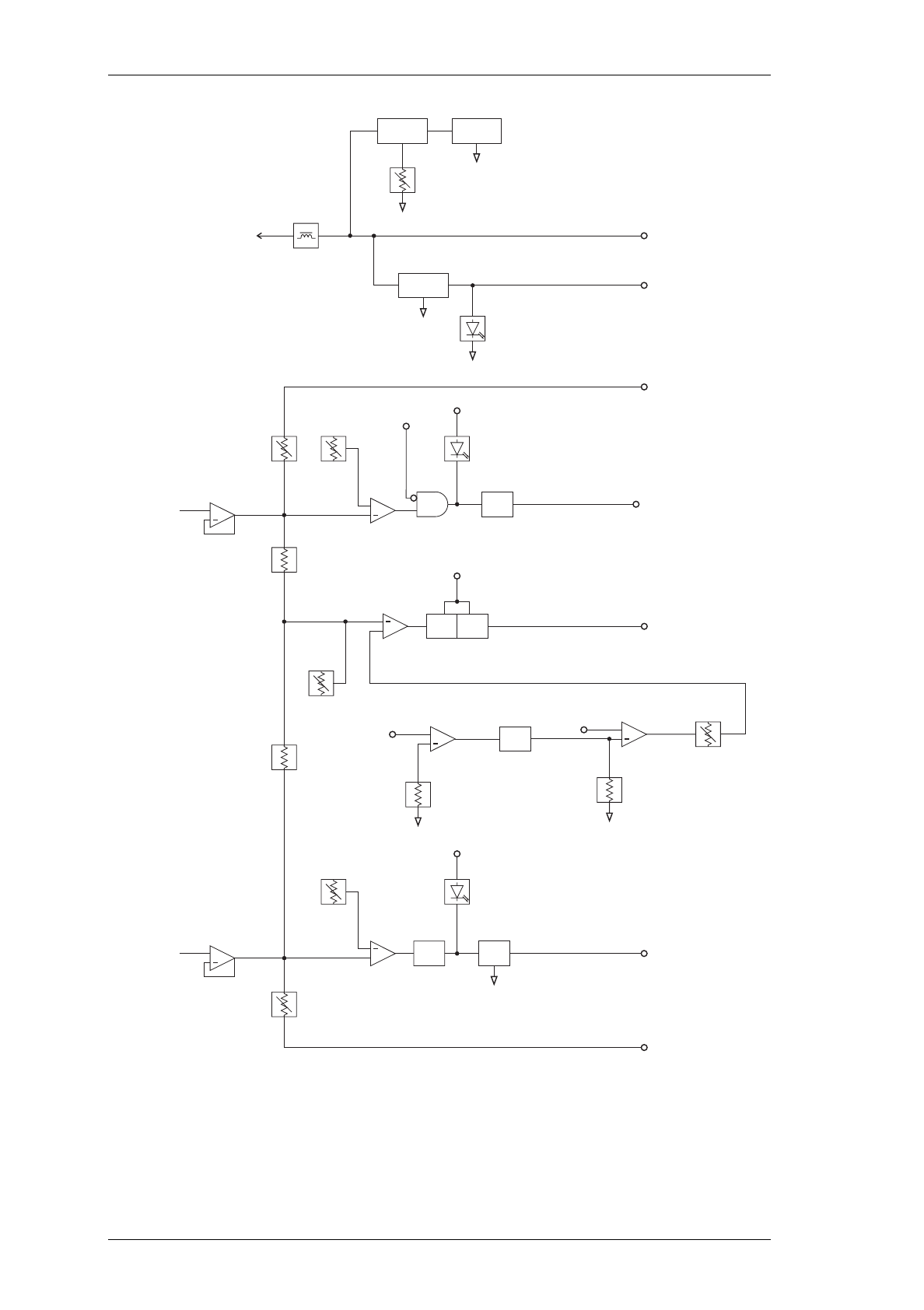
D2.6
T858/859 Circuit Operation
M850-00
24/01/00 Copyright TEL
Figure 2.4 T859 Control Circuitry Block Diagram
RV115
IC140 IC110
Drive Level Clamp
+Q200
-t° R200
NTC
Shutdown
Power Level
Comparator
IC200 RV113
Ref. +
-t° R210
NTC
Comparator
IC105
Ref.
(#IC210 mounting flange) (low pass filter section)
+
Comparator
Q100 Q101
FET
Switch
+
+
+
Comparator
FET
Switch
Q102
IC100
RV105
High Reverse Power LED
Low Forward Power LED
Reverse
Power
Meter
Reverse
Power
Alarm
Forward
Power
Meter
Forward
Power
Alarm
+7V
+7V
Tx
Key
IC100
RV101
RV103
+
Q128Q124
Q103
+13.8V
Filtered
Integrator
IC110
Control
Supply
RV109
Power
Control
R107
RV107
R106
Reverse
Power
Sense
Buffer
IC100
Buffer
IC100
Forward
Power
Sense
7V
Supply
13.8V
Filtered
L162/L161
13.8V
Supply LED
IC130
Voltage
Regulator
Forward Power
Alarm
Reverse Power
Alarm

M850-00
T858/859 Circuit Operation
D2.7
Copyright TEL 24/01/00
2.3.1 Power Control
The DC voltages from the directional coupler representing forward and reflected power
are buffered by the two voltage followers, IC103 [IC100] pins 1, 2 & 3 and pins 12, 13 &
14. Their outputs are summed at an integrator (IC105 [IC110] pins 1, 2 & 3), which
drives the series pass control elements (Q135 & Q137 [Q124 & Q128]).
Forward and reflected power are summed so that, under high output VSWR, the power
control turns the PA down. This is because the control loop adjusts for the same DC
voltage from the directional coupler that would have been present if there were no
reflected power.
2.3.2 Driver Power Level
The maximum output power of the T858/859 can be limited by placing a ceiling on the
driver output power level using RV115 (accessible through the side cover). For exam-
ple, if RV115 is set for a maximum output power of 50W, the range of adjustment using
RV109 (front panel power adjust) will be 20 to 50W.
Caution:
The driver power level clamp (RV115) is factory set to give a maximum
power output at room temperature of 60W for the T858 and 110W for
the T859. The unit may be damaged if this level is increased.
2.3.3 Thermal Protection
At excessively high temperatures, the output power will automatically reduce to a pre-
set level (set by RV113), thus preventing the PA from overheating.
Ambient temperature within the PA is measured by a thermistor controlled voltage
divider (R168 [R177], R210) which applies a voltage to a comparator with hysteresis
(IC101 [IC105] pins 8, 9 & 10). This thermistor is located on the PCB in the low pass fil-
ter cavity.
Thermal protection is also provided for the RF power module to prevent the module
itself from overheating. This protection consists of a thermistor controlled voltage
divider (R203, R215 [R200]) which sets a voltage on a comparator with hysteresis (IC200
pins 1, 2 & 3). The thermistor is located on the module flange.
The output current from all comparators is summed into the power control network via
RV113 so that the power level to which the PA must turn down may be set.
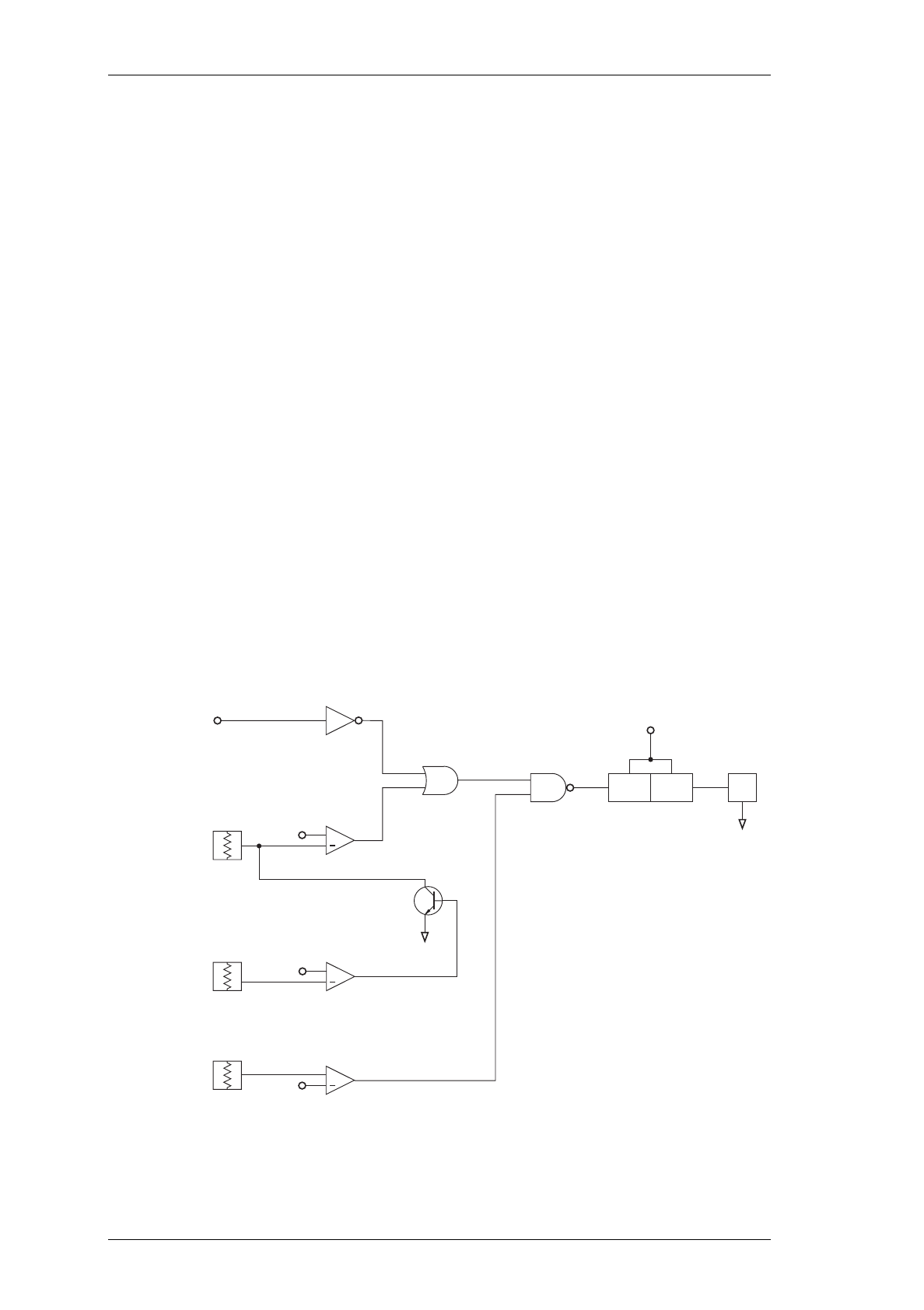
D2.8
T858/859 Circuit Operation
M850-00
24/01/00 Copyright TEL
2.3.4 Forward And Reverse Power Alarms
If forward power drops below, or reverse power rises above, presettable limits, alarms
may be triggered.
The alarm outputs are open drain configuration and are low under normal conditions
(i.e. forward and reverse power levels are normal).
IC103 [IC100] pins 5, 6 & 7 and pins 8, 9 & 10 form comparators with thresholds
adjusted via RV101 (forward power) and RV105 (reverse power) respectively. The
inputs are from the forward and reverse power signals from the directional coupler,
buffered by IC103 [IC100] pins 1, 2 & 3 and pins 12, 13 & 14. Thus, the power levels at
which the forward and reverse power alarms are triggered are defined by RV101 and
RV105 respectively.
2.3.5 Forward And Reverse Power Metering
Forward and reverse power signals from the two IC103 [IC100] buffers are available for
metering purposes. The output currents are adjustable via RV103 (forward power) and
RV107 (reverse power).
2.3.6 T859 Fan Control Circuitry
Figure 2.5 T859 Fan Control Logic Diagram
Q113 Q114 Fan
Ref +
High Temp.
Sense On PCB
Comparator
IC105
R210
High Temp.
Sense On
Module Flange
Low Temp.
Sense
NTC
Tx Key
Invert
Q110 OR
Q111,
R140, R141
Q200
NAND
Q111, Q112,
R142, R143 Fan Driver
13.8V
Filtered
Ref +
Comparator
IC200
R200
NTC
Comparator
Ref +
IC105
R127
NTC
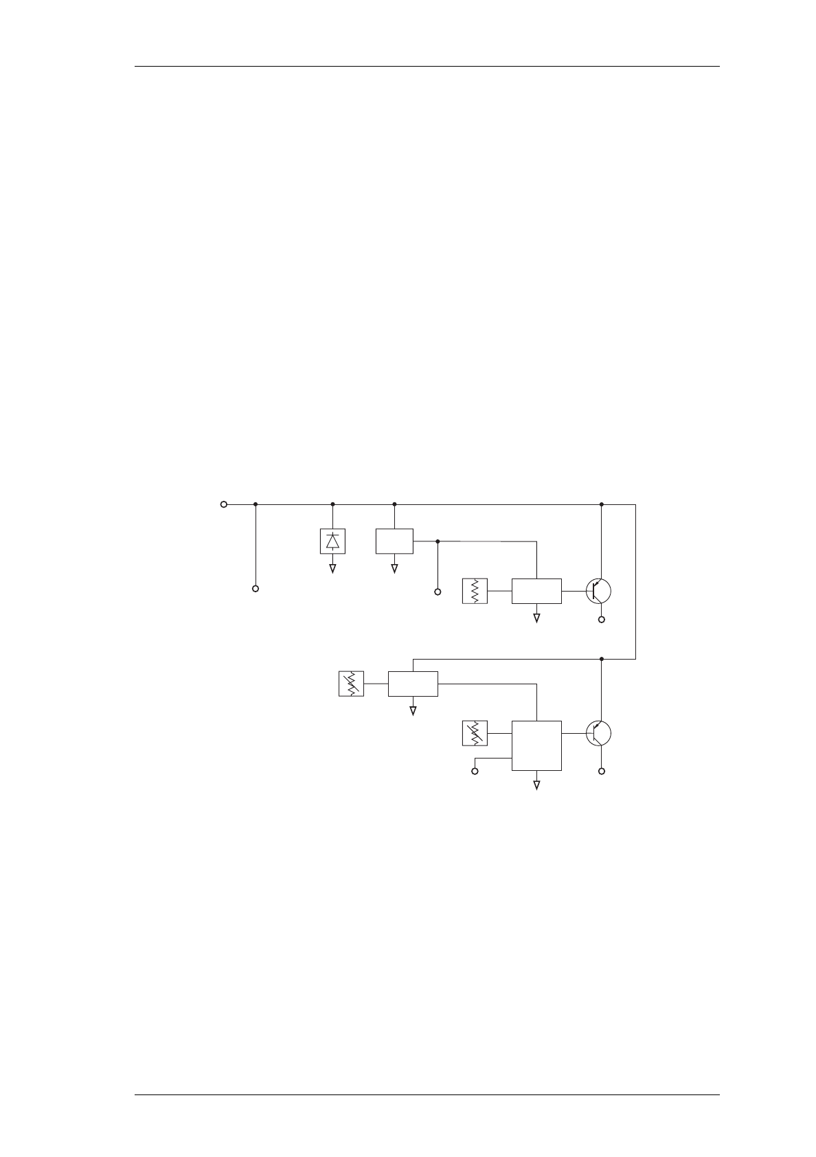
M850-00
T858/859 Circuit Operation
D2.9
Copyright TEL 24/01/00
Comparator IC105 pins 12, 13 & 14 are set to switch at heatsink temperatures greater
than +90°C or RF power module flange temperatures greater than +110°C, and pins 1, 2
& 3 at temperatures less than -10°C.
A logic AND function is applied to the comparator outputs by Q111 and Q112, thereby
turning on the fan unconditionally (via Q113 and Q114) if the heatsink temperature
exceeds +90°C or the module flange temperatures exceed +110°C.
A logic OR function is applied to comparator IC105 pins 12, 13 & 14 and Tx KEY signals,
thereby turning on the fan when the transmitter is keyed and the temperature is
between -10°C and +90°C (or +110°C for the module flanges).
If the temperature drops below -10°C, Q112 is turned off, preventing Q111 from activat-
ing the fan.
2.4 Power Supply & Regulator Circuits
(Refer to the control section circuit diagram in Section 5.)
Figure 2.6 T858/859 Power Supply & Regulator Circuitry Block Diagram
The T858/859 are designed to operate off a 10.8-16V DC supply (13.8V nominal). A 7V
supply runs directly off the 13.8V rail, driving the fan control, power control and alarm
circuitry.
A crowbar diode is fitted for protection against connection to a power supply of incor-
rect polarity. It also provides transient overvoltage protection.
Note:
A fuse must be fitted in the power supply line for the diode to provide effec-
tive protection.
7V
Reg.
Fan
Control
Power
Clamp
Power
Control
Crowbar
Diode
Temp.
Sense
To Fan
+7V
Clamp
Power
From
Directional
Coupler
Power
Control
Vout
Set
Power
13.8V
Nom.

D2.10
T858/859 Circuit Operation
M850-00
24/01/00 Copyright TEL
M850-00
T858/859 Initial Adjustment
D3.1
Copyright TEL 24/01/00
3 T858/859 Initial Adjustment
Caution:
This equipment contains CMOS devices which are susceptible to dam-
age from static charges. Refer to Section 1.2 in Part A for more infor-
mation on anti-static procedures when handling these devices.
The following section describes the full adjustment procedure to be carried out before
operating the T858/859.
Note 1:
The T858/859 requires no RF tuning or alignment.
Note 2:
Where the same component has different circuit references in the T858 and
T859, in this and following sections the T858 circuit reference is given first,
followed by the T859 circuit reference in brackets, e.g. Q137 [Q128].
Refer to Section 5 where the parts lists, grid reference index and diagrams will provide
detailed information on identifying and locating components.
The following topics are covered in this section.
Section Title Page
3.1 Test Equipment Required 3.3
3.2 Shorting Links 3.3
3.3 Preliminary Checks 3.4
3.4 Setting The Output Power 3.4
3.5 High Temperature Shutdown Power Level 3.5
3.6 Remote Forward Power Meter Calibration 3.5
3.7 Remote Reverse Power Meter Calibration 3.5
3.8
3.8.1
3.8.2
Setting Alarm Levels
Forward Power
Reverse Power
3.6
3.6
3.6
Figure Title Page
3.1 T858/859 Test Equipment Set-up 3.3

D3.2
T858/859 Initial Adjustment
M850-00
24/01/00 Copyright TEL

M850-00
T858/859 Initial Adjustment
D3.3
Copyright TEL 24/01/00
3.1 Test Equipment Required
• DC power supply capable of delivering >16A (T858) or >20A (T859) at 13.8V.
• Multimeter or DMM (e.g. Fluke 77).
• RF power meter (e.g. HP 435 series or Bird Wattmeter).
• 150W 30dB attenuator (T858) or 250W 50dB attenuator (T859).
• 150W 3dB 50 ohm pad.
• 'BNC' to 'N' type adaptors (e.g. Amphenol, Greenpar).
• Appropriate trimming tools.
Figure 3.1 T858/859 Test Equipment Set-up
Caution:
Do not connect attenuators or DC blocks between the T857 and T858/
859 or the cyclic keying circuitry will not function correctly.
3.2 Shorting Links
There are seven shorting links on PL110 in the control section circuitry, as described in
the table below. Ensure that these links are set as standard before starting and after
completing the adjustment procedure.
Link Pins Standard Setting Function
1-2, 3-4,
7-8, 9-10
not linked Not used.
5-6 not linked Pins 5-6 are provided for simulating high
operating temperatures during initial
adjustment. Bridging this link shorts out
R215 [R200] and R210 (NTCs), thus turning
on the thermal protection circuitry. They
should not be linked for normal operation.
11-12
13-14
linked Pins 11-12 and 13-14 are provided for fac-
tory testing only. The PA will not function
correctly if these settings are changed.
Exciter PA
Tx Key
RF Power
Meter
Tx Enable
30db
Attenuator
(HP 435)

D3.4
T858/859 Initial Adjustment
M850-00
24/01/00 Copyright TEL
3.3 Preliminary Checks
Check for short circuits between the positive rail and earth.
Set up the test equipment as in Figure 3.1.
Connect the T858/859 to a 13.8V DC supply.
Check that the quiescent current is <50mA.
To key the transmitter, earth the key line (pin 13) on the exciter.
Check that the power supply is still at 13.8V under load.
Check that the regulated power control supply is approximately 7V.
Note:
The output power and alarm levels should be set with the side cover on. If
the cover is removed for other adjustment procedures, make a final check of
the output power and alarm levels with the side cover on.
3.4 Setting The Output Power
Caution:
If the high temperature shutdown power level has not yet been set or is
unknown, check that the unit does not overheat while setting the out-
put power.
Note 1:
Cables and connectors can easily cause a power loss of several watts if either
too long or poorly terminated. Always use the shortest possible leads (or
connectors instead of leads) between the T858/859 and power meter set-up.
Note 2:
You will need appropriate extension leads if you wish to carry out the
adjustment procedures with the T858/859 withdrawn from the rack in the
latched position. Alternatively, disconnect and withdraw the T858/859 and
reconnect it behind the rack.
Note 3:
The actual power used may be limited by regulatory requirements.
Connect the exciter output to the PA input via a thru-line wattmeter with a 5W
full scale reading. Special BNC/N leads will be required.
Ensure that PL110 pins 11-12 and 13-14 are linked, and all other pins are not
linked.
Connect an RF power meter to the PA output via a 30dB pad.
Set RV109 [%RV109] (front panel power control) and RV115 (driver power clamp)
fully clockwise.
Key on the drive source.

M850-00
T858/859 Initial Adjustment
D3.5
Copyright TEL 24/01/00
Check that the power output exceeds:
T858 - 60W
T859 - 120W.
Note:
The side cover access hole for the driver power clamp (RV115) is covered
with a tamper-proof sticker. The clamp has been factory set to 60W (T858)/
110W (T859) maximum output power and should not normally need
adjustment. If the output power level is low, check that the high tempera-
ture shutdown circuit has not activated by verifying that IC101 [IC105] pin 8
is low.
Adjust RV115 to reduce the maximum power output to:
T858 - 60W
T859 - 110W.
Adjust RV109 [%RV109] to set the power output to the required level (e.g. 50W for
the T858, 100W for the T859).
3.5 High Temperature Shutdown Power Level
Set RV109 [%RV109] (front panel power control) to the required output power.
Simulate high operating temperatures by placing a shorting link on PL110 pins 5-6
(do not use either of the links from PL110 pins 11-12 or 13-14 to do this).
Adjust RV113 (shutdown power level) for an output power of:
T858 - 20W
T859 - 40W.
Remove the shorting link from PL110 pins 5-6 to return the PA to normal opera-
tion.
3.6 Remote Forward Power Meter Calibration
If a remote meter is connected, adjust RV103 (forward power meter calibration)
for the remote reading to agree with the RF power meter reading.
3.7 Remote Reverse Power Meter Calibration
If a remote meter is connected, connect a 50 ohm 3dB pad (with the output open
circuit) to the PA output.
Apply RF drive and Tx-Key.
Adjust RV107 (reverse power meter calibration) for a quarter of the forward
power reading.

D3.6
T858/859 Initial Adjustment
M850-00
24/01/00 Copyright TEL
3.8 Setting Alarm Levels
Note:
If forward and reverse power metering is being used, set up their calibration
(Section 3.6 and Section 3.7) before setting the alarm levels.
3.8.1 Forward Power
Power up the T858/859 and adjust RV109 [%RV109] (front panel power control)
so that the output power is at the alarm level required (e.g. 40W if the T858 nor-
mally operates at 50W).
Adjust RV101 (forward power alarm set) so that the forward power alarm LED
lights.
Check the alarm level setting by adjusting the power up and down and observing
the alarm LED. A few watts hysteresis can be expected.
Readjust RV109 [%RV109] for the normal operating level.
Note:
Remote indication is available at pin 3 of D-range 1.
3.8.2 Reverse Power
Power up the T858/859 and adjust RV109 [%RV109] (front panel power control)
for the normal operating power level.
Place a known mismatch of the required value (e.g. 3:1 VSWR) and adjust RV105
(reverse power alarm set) so that the reverse power alarm LED lights.
Example:
A VSWR of 3:1 can be simulated by connecting an unterminated 3dB pad
(50W) to the PA output. This will result in a return loss of 6dB.
Note:
Remote indication is available at pin 4 of D-range 1.

M850-00
T858/859 Fault Finding
D4.1
Copyright TEL 24/01/00
4 T858/859 Fault Finding
Caution:
This equipment contains CMOS devices which are susceptible to dam-
age from static charges. Refer to Section 1.2 in Part A for more infor-
mation on anti-static procedures when handling these devices.
The following test procedures and fault finding flow charts may be used to help locate a
hardware problem, however they are by no means a complete fault finding procedure.
If you still cannot trace the fault after progressing through them in a logical manner,
contact your nearest Tait Dealer or Customer Service Organisation. If necessary, you
can get additional technical help from Customer Support, Radio Systems Division, Tait
Electronics Ltd, Christchurch, New Zealand (full contact details are on page 2).
Note:
Where the same component has different circuit references in the T858 and
T859, in this and following sections the T858 circuit reference is given first,
followed by the T859 circuit reference in brackets, e.g. Q137 [Q128].
Refer to Section 5 where the parts lists, grid reference index and diagrams will provide
detailed information on identifying and locating components.
The following topics are covered in this section.
Section Title Page
4.1 Visual Checks 4.3
4.2 Shorting Links 4.3
4.3 Component Checks 4.3
4.4 DC Checks 4.4
4.5
4.5.1
4.5.2
RF Checks
T858
T859
4.4
4.4
4.5
4.6
4.6.1
4.6.2
4.6.3
4.6.4
4.6.5
Fault Finding Charts
T858 PA
T859 PA
T858 Power Control
T859 Power Control
T859 Fan Control Circuitry
4.9
4.9
4.10
4.11
4.12
4.13
4.7 Replacing RF Power Transistors 4.14
4.8 Replacing RF Power Modules 4.16
4.9 Removing The PCB From The Heatsink 4.17

D4.2
T858/859 Fault Finding
M850-00
24/01/00 Copyright TEL
Figure Title Page
4.1
4.2
T858/859 Test Break Point Location
Typical Capacitor Positioning On T858/859 RF Power Transis-
tors
4.7
4.14

M850-00
T858/859 Fault Finding
D4.3
Copyright TEL 24/01/00
4.1 Visual Checks
Remove the side cover from the T858/859 and inspect the PCB for damaged or
broken components, paying particular attention to the surface mounted devices
(SMDs). Also check for defective solder joints.
Refer to Section 4.7, Section 4.8, Section 4.9 and Section 3 of Part A for more details
on repair and replacement of components.
4.2 Shorting Links
There are seven shorting links on PL110 in the control section circuitry, as described in
the table below. Ensure that these links are set as standard before starting and after
completing the adjustment procedure.
4.3 Component Checks
If you suspect a transistor is faulty, you can assess its performance by measuring the for-
ward and reverse resistance of the junctions. Unless the device is completely desol-
dered, first make sure that the transistor is not shunted by some circuit resistance (e.g. a
base choke). Use a good quality EVM (e.g. Fluke 75) for taking the measurements (or a
20k ohm/V or better multimeter, using only the medium or low resistance ranges).
Caution:
Before operating the PA, replace any RF base chokes removed while
making measurements.
The collector current drawn by multi-junction transistors is a further guide to their per-
formance.
Link Pins Standard Setting Function
1-2, 3-4,
7-8, 9-10
not linked Not used.
5-6 not linked Pins 5-6 are provided for simulating high
operating temperatures during initial
adjustment. Bridging this link shorts out
R215 [R200] and R210 (NTCs), thus turning
on the thermal protection circuitry. They
should not be linked for normal operation.
11-12
13-14
linked Pins 11-12 and 13-14 are provided for fac-
tory testing only. The PA will not function
correctly if these settings are changed.

D4.4
T858/859 Fault Finding
M850-00
24/01/00 Copyright TEL
If an IC is suspect, the most reliable check is to measure the DC operating voltages. Due
to the catastrophic nature of most IC failures, the pin voltages will usually be markedly
different from the recommended values in the presence of a fault. The recommended
values can be obtained from either the circuit diagram or the component data catalogue.
4.4 DC Checks
Note:
No RF power is to be applied during these checks.
Check that +13.8V is present on the collectors of Q216 (T858) or Q216 and Q217
(T859). Make this measurement when the transmitter is not keyed.
Check that approximately 8-13.8V is present on pin 2 of #IC210 (the level is
dependent on RV115 being set to maximum).
Check that +13.8V is present at pin 4 of IC100.
Check that approximately +12V is present at pin 8 of IC110 (the level is dependent
on RV115 being set to maximum).
Check that +7.0V is present at the output of regulator IC130.
4.5 RF Checks
4.5.1 T858
The T858 PA Fault Finding Chart (Section 4.6.1) provides a systematic approach for
locating a fault in the RF circuitry. Use this chart in conjunction with Figure 4.1, which
shows the locations of the 50Ω input and output test points for RF module #IC210 and
RF transistor Q216.
Note 1:
Use good quality 50Ω coax for the "flying" test leads.
Note 2:
Ensure each output is terminated in a 50Ω load of the correct power rating.
For problems with the power control circuitry, refer to the T858 Power Control Fault
Finding Chart (Section 4.6.3).
Device Input Connection Output Connection
#IC210 input BNC connector or SK201 C249
Q216 C249 C250

M850-00
T858/859 Fault Finding
D4.5
Copyright TEL 24/01/00
4.5.2 T859
The T859 PA Fault Finding Chart (Section 4.6.2) provides a systematic approach for
locating a fault in the RF circuitry. Use this chart in conjunction with Figure 4.1, which
shows the locations of the 50Ω input and output test points for RF module #IC210 and
RF transistors Q216 and Q217.
Note 1:
Use good quality 50Ω coax for the "flying" test leads.
Note 2:
Ensure each output is terminated in a 50Ω load of the correct power rating.
For problems with the power control circuitry, refer to the T859 Power Control Fault
Finding Chart (Section 4.6.4).
Device Input Connection Output Connection
#IC210 input BNC connector or SK201 C274
Q216 & Q217 L241 C250, C262

D4.6
T858/859 Fault Finding
M850-00
24/01/00 Copyright TEL

M850-00
T858/859 Fault Finding
D4.7
Copyright TEL 24/01/00
replace A4 pages D4.7/D4.8 with A3 pages D4.7/D4.8
Figure 4.1 T858/859 Test Break Point Location
unavailable at time of publication

D4.8
T858/859 Fault Finding
M850-00
24/01/00 Copyright TEL
replace A4 pages D4.7/D4.8 with A3 pages D4.7/D4.8

M850-00
T858/859 Fault Finding
D4.9
Copyright TEL 24/01/00
4.6 Fault Finding Charts
4.6.1 T858 PA
RF circuitry OK.
N
N
Y
Y
Y
Y
Are RV115 & RV109
fully clockwise? NRotate clockwise:
RV109 first, RV115 second.
Is the drive from the
exciter 700mW-1.3W? Repair exciter.
Is #IC210 output >30W?
(see Figure 4.1) N
With no RF present,
check collectors >13V.
Check for shorts around
transistor base matching caps.
Check transistor junction
resistance (see Section 4.3).
Q216 output >60W? N
Check components in LPF.
Check output N-type connector
for short circuit or excessive wear.
Replace parts as necessary.
YIs maximum power >60W
over entire frequency range?* N
Set RV115 (driver power clamp)
to 60W (refer Section 3.4). Y
Is maximum power >60W
over entire frequency range?*
Return PA to your local
Tait service centre.
N
Y
*Frequency Ranges
T858-10: 400-440MHz
T858-20: 440-480MHz
T858-30: 480-520MHz
Check #IC210 pin 4 >13V.
Check #IC210 pins 2 & 3 >12V.
Check C228, R227, R226,
R230 & C249.
Check SK201 for short.
Replace module.
Is maximum power >60W
over entire frequency range?*
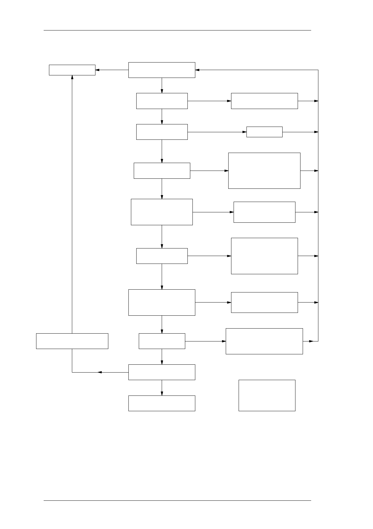
D4.10
T858/859 Fault Finding
M850-00
24/01/00 Copyright TEL
4.6.2 T859 PA
RF circuitry OK.
Return PA to your local
Tait service centre.
N
N
Y
Y
Y
N
N
Is maximum power >100W
over entire frequency range?*
Is maximum power >100W
over entire frequency range?*
Y
Y
Y
YCheck components in LPF.
Check output N-type connector
for short circuit or excessive wear.
Replace parts as necessary.
With no RF present,
check collectors >13V.
Check for shorts around
transistor base matching caps.
Check transistor junction
resistance (see Section 4.3).
N
Is the drive from the
exciter 700mW-1.3W? Repair exciter.
Is #IC210 output >30W?
(see Figure 4.1) N
Check #IC210 pin 4 >13V.
Check #IC210 pins 2 & 3 >12V.
Check C228, R227, R226,
R230 & C274.
Check SK201 for short.
Replace module.
Check the condition of
splitter hybrid L241.
Are there any shorts
between the splitter pads?
Y
N
Q216, Q217
outputs each >60W?
Y
N
Check the condition of
combiner hybrid L240.
Are there any shorts
between the combiner pads?
N
Is R240 hot to touch
when PA keyed?
*Frequency Ranges
T859-10: 400-440MHz
T859-20: 440-480MHz
T859-30: 480-520MHz
Set RV115 (driver power clamp)
to 110W (refer Section 3.4).
Are RV115 & %RV109
fully clockwise? Rotate clockwise:
%RV109 first, RV115 second.
Return PA to your Customer
Service Organisation for
splitter hybrid replacement.
Return PA to your Customer
Service Organisation for
combiner hybrid replacement.
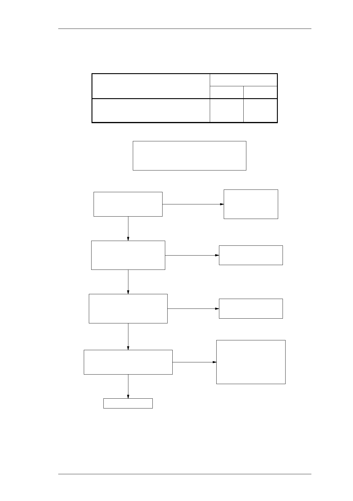
M850-00
T858/859 Fault Finding
D4.11
Copyright TEL 24/01/00
4.6.3 T858 Power Control
Approximate voltages (@ 480MHz) under normal operating conditions:
Forward & Reverse Power
Measurement
Output Power
20W 50W
forward power at IC100 pin 14
reverse power at IC100 pin 1
1.8V
0.6V
2.9V
0.6V
N
Check 12V DC present
on IC105 pin 8.
Check sense voltages
from directional coupler.
Check IC103 pins 1 & 14.
The following voltage checks are all done with
RV115 (driver power clamp) set to maximum.
When these tests are finished, reset RV115 to 60W.
Caution
Using RV109, does output power
adjust over the range 10-50W?
RF Power Level Control Check
Check Q117 & Q121.
Check IC103 pin 8 >12V DC
when forward power low.
Low Forward Power Alarm Check
Y
Y
Does high reverse power alarm
LED light when PA operated into
a mismatch of 3:1 or worse?
Check Q129 & Q131.
Check IC103 pin 7 >12V DC
when reverse power high.
High Reverse Power Alarm Check
N
Y
At high operating temperatures,
does the output power reduce to 20W?
Over-Temperature Shutdown Check N
Y
Power control OK.
Using RV109, does low forward
power alarm LED light when
output power reduced to 30W?
N
Place a shorting link on
pins 5 & 6 of PL110.
Check IC101 pin 8 >12V DC.
Check Q133 collector goes from
2.8V to 0V when PL110
pins 5 & 6 are shorted.
Remove link from PL110
pins 5 & 6 when finished.
D4.12
T858/859 Fault Finding
M850-00
24/01/00 Copyright TEL
4.6.4 T859 Power Control
Approximate voltages (@ 480MHz) under normal operating conditions:
Forward & Reverse Power
Measurement
Output Power
40W 100W
forward power at IC100 pin 14
reverse power at IC100 pin 1
2.5V
0.6V
4.2V
0.6V
Caution
RF Power Level Control Check
Low Forward Power Alarm Check
Y
Y
Does high reverse power alarm
LED light when PA operated into
a mismatch of 3:1 or worse?
High Reverse Power Alarm Check
N
Y
Over-Temperature Shutdown Check N
Y
Power control OK.
N
The following voltage checks are all done with
RV115 (driver power clamp) set to maximum.
When these tests are finished, reset RV115 to 110W.
Using %RV109, does output power
adjust over the range 20-100W?
Check 12V DC present
on IC110 pin 8.
Check sense voltages
from directional coupler.
Check IC100 pins 1 & 14.
N
Using %RV109, does low forward
power alarm LED light when
output power reduced to 60W?
Check Q102 & Q103.
Check IC100 pin 8 >12V DC
when forward power low.
Check Q100 & Q101.
Check IC100 pin 7 >12V DC
when reverse power high.
At high operating temperatures,
does the output power reduce to 40W?
Place a shorting link on
pins 5 & 6 of PL110.
Check IC105 pin 8 >12V DC.
Check Q135 collector goes from
2.8V to 0V when PL110
pins 5 & 6 are shorted.
Remove link from PL110
pins 5 & 6 when finished.
M850-00
T858/859 Fault Finding
D4.13
Copyright TEL 24/01/00
4.6.5 T859 Fan Control Circuitry
Key transmitter.
Does fan run at
room temperature?
Does the low temperature
inhibit circuit stop the fan?
N
N
Y
Y
Do not key
transmitter.
Does hi
g
h temperature control
circuit activate fan? N
Y
Fan control OK.
Place shortin
g
link on PL110
pins 5 & 6 (see Section 3.5).
Remove the shortin
g
link
from PL110 pins 5 & 6.
Check Q111 & Q112 collector
volta
g
es. Check Q113 & Q114.
Check IC105 pin 1 <1V.
Check Q110.
Check Tx-Key is low (at
g
round).
Spray "freeze" on R127
or short R133.
Spray "freeze" on R127
OR short R133.
Check IC105 pin 1 >11V.
Check Q112 & Q111.
Place shortin
g
link on PL110
pins 5 & 6 (see Section 3.5).
Check IC105 pin 14 >11V.
Check Q112 & Q111.
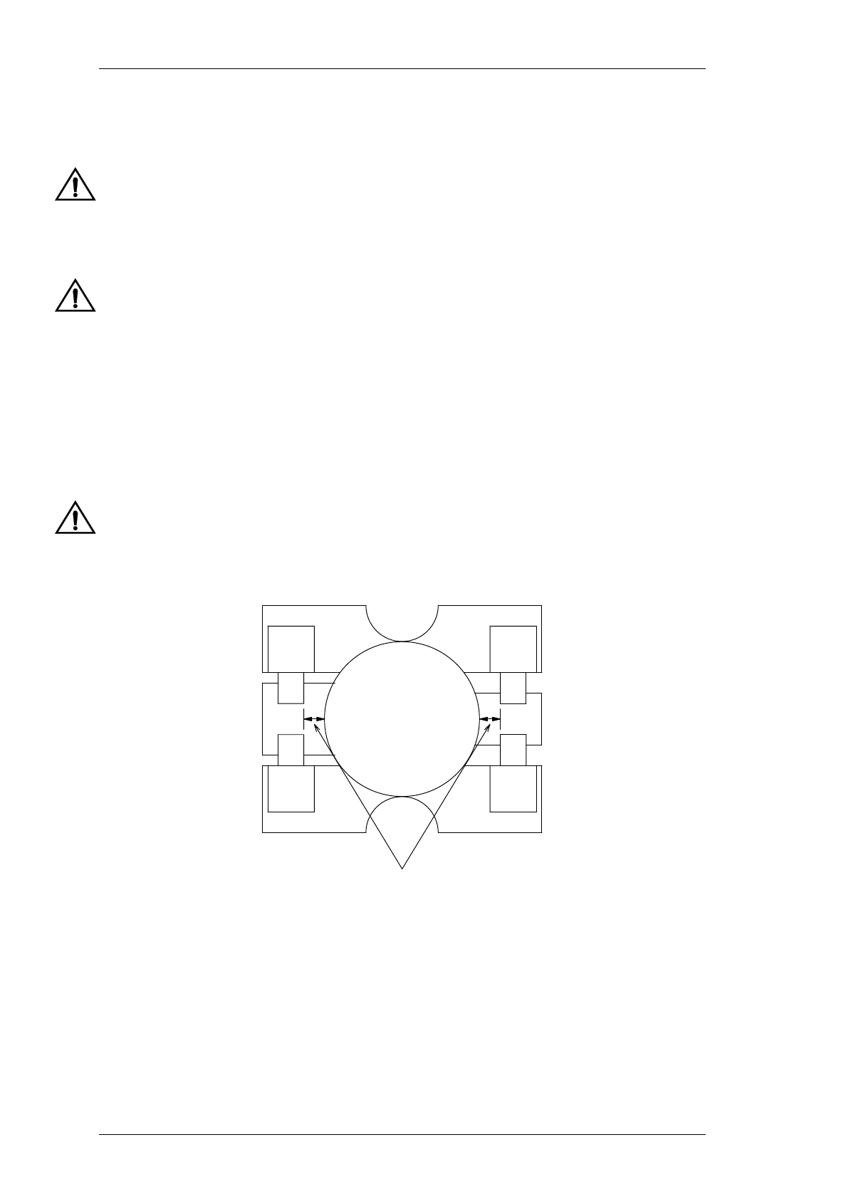
D4.14
T858/859 Fault Finding
M850-00
24/01/00 Copyright TEL
4.7 Replacing RF Power Transistors
Caution:
Failure to comply with the following procedure can result in failure of
the device due to poor heatsinking, or worse, can endanger the health
of the assembler if the beryllium oxide die carrier is smashed during
assembly.
Caution:
As the location of certain components in the PA is critical to perform-
ance, it is important that any components removed or disturbed are
refitted in exactly the same position.
Before attempting to remove a transistor, note the position, type and
value of each capacitor. Measure the distance between each capacitor
and the transistor body to the nearest 0.5mm (measurement "A" in Fig-
ure 4.2) so that it can be replaced in exactly the same position. These
measurements are shown for the T858, however the same procedure
applies for the T859.
Caution:
Do not apply too much heat or pressure to the PCB pads and tracks as
you may damage them or lift them from the PCB, causing permanent
damage to the PA.
Figure 4.2 Typical Capacitor Positioning On T858/859 RF Power Transistors
(Not To Scale)
Desolder and remove the capacitors from around the transistor.
Remove the two mounting screws, then desolder and remove the two solder tags.
Desolder the transistor tabs by heating with a soldering iron and lifting away
from the PCB with a screwdriver or thin stainless steel spike, then remove the
device.
base collector
measurement A

M850-00
T858/859 Fault Finding
D4.15
Copyright TEL 24/01/00
Remove any excess solder from the PCB pads with solder wick.
Trim the tabs of the replacement transistor so that the device sits neatly on the
PCB pads provided.
Lightly tin the underside of the transistor tabs. Remove any excess solder to leave
a thin, even layer on the tabs.
Apply a small amount of heatsink compound (Dow-Corning 340 or equivalent) to
the transistor mounting surface. Sufficient compound should be used to ensure
an even film over the entire mounting surface.
Place the transistor on the PCB in the correct orientation and ensure the tabs are
flush to the surface.
Solder all transistor tabs to the PCB.
Refit the solder tags and mounting screws. Tighten the screws to a torque of
90N.cm/8in.lbf.
Replace each capacitor in exactly the same position as noted previously.

D4.16
T858/859 Fault Finding
M850-00
24/01/00 Copyright TEL
4.8 Replacing RF Power Modules
Caution:
Follow these instructions carefully, otherwise the module can fail
because of poor heatsinking or cracked substrates.
Desolder the module legs by heating with a soldering iron and lifting away from
the PCB with a screwdriver or thin stainless steel spike.
Undo the module screws and remove the thermistor assembly.
Desolder and remove both earth tags.
Gently lift the module away from the heatsink.
Note:
The module may be stuck down quite firmly with heatsink compound. You
may need to carefully prise it away from the heatsink with a small screw-
driver. Keep the heatsink compound clean while the module is detached.
Apply a small amount of heatsink compound (Dow-Corning 340 or equivalent) to
the replacement module mounting surface. Use enough compound to ensure an
even film over the entire mounting surface.
Reposition the module in the correct orientation and ensure it is well pasted to the
heatsink.
Replace the earth tags and thermistor assembly in their original positions and
hand-tighten the screws, ensuring the tags and thermistor remain in place. Alter-
nately tighten each screw evenly, finally torquing them down to 56N.cm/5in.lbf.
with an accurate torque driver.
Caution:
It is essential that you apply the correct torque to these screws to allow
the module flange to expand and contract under temperature cycling.
Also, do not solder any module legs before torquing down otherwise
the device may be broken.
Solder the earth tags and all module legs to the PCB.

M850-00
T858/859 Fault Finding
D4.17
Copyright TEL 24/01/00
4.9 Removing The PCB From The Heatsink
Note:
This is a lengthy procedure and should be considered only after all other
checks have been carried out. There are no components on the bottom of the
PCB.
Remove the harmonic filter shield lid.
T859 Only: Desolder the power feed to the fan from the PCB.
Remove the 50 ohm output N-type connector by unscrewing it from the heatsink
casting and desoldering it from the PCB.
Unplug the 50 ohm input coaxial cable from the PCB, unscrew the BNC connector
from the heatsink, and remove the connector and cable.
Desolder the positive and negative power feed wires from the D-range PCB.
Disconnect the ribbon cable from the D-range PCB.
Remove the two screws securing the D-range connector and PCB to the heatsink
and withdraw the assembly from the heatsink.
Remove the mounting screws for the TO-220 devices:
T858 Q137
T859 Q128, R231 and R240.
Remove the two screws securing the power module (#IC210).
Remove the mounting screws for the power transistors:
T858 Q216
T859 Q216 and Q217.
Remove the PCB retaining screws:
T858 13
T859 17.
Push the three LEDs out of their front panel grommets.
Lift the PCB gently from the heatsink to gain access to the underside of the board.
Note:
R231, R240 and #IC210 may be stuck down with heatsink compound. You
may need to carefully prise them away from the heatsink with a small
screwdriver.
Caution:
Keep the heatsink compound clean while the PCB is detached. Any
objects caught in the heatsink compound underneath the device which
prevent effective earthing and/or heatsinking may cause the device to
fail.

D4.18
T858/859 Fault Finding
M850-00
24/01/00 Copyright TEL
Caution:
Do not operate the PA with the PCB detached as the heatsink is used
for earthing and heat dissipation.
To replace the PCB, reverse the order of removal, taking care that the wiring is cor-
rectly positioned and not 'pinched'.
Make sure that the heatsink compound has stayed clean, and that the insulating
pad for Q137 [Q128] is not damaged.
If you have difficulty refitting the LEDs, try pushing the body of the LED back
into the grommet with a thin screwdriver or spike.

IPN 220-01422-03
M850-00
T859 PCB Information
D5.3.17
Copyright TEL 24/01/00
T859 Parts List (IPN 220-01422-03)
How To Use This Parts List
The components listed in this parts list are divided into two main types: those with a circuit reference (e.g. C2, D1, R121, etc.) and
those without (miscellaneous and mechanical).
Those with a circuit reference are grouped in alphabetical order and then in numerical order within each group. Each component
entry comprises three or four columns: the circuit reference, variant (if applicable), IPN and description. A number in the variant col-
umn indicates that this is a variant component which is fitted only to the product type listed. Static sensitive devices are indicated by
an (S) at the start of the description column.
The miscellaneous and mechanical section lists the variant and common parts in IPN order. Where possible, a number in the legend
column indicates their position in the mechanical assembly drawing.
The Parts List Amendments box below lists component changes that took place after the parts list and diagrams in this section were
compiled. These changes (e.g. value changes, added/deleted components, etc.) are listed by circuit reference in alphanumeric order
and supersede the information given in the parts list or diagrams. Components without circuit references are listed in IPN order.
Parts List Amendments
C142 Changed from 4n7 (IPN 015-24470-08) to 33nF (IPN 015-25330-08) to improve cyclic keying (711105).
C147 Changed from 1nF (IPN 015-24100-08) to 33nF (IPN 015-25330-08) to improve cyclic keying (711104).
C173 Deleted - not required for circuit performance (711141).
#C247, #C273 T859-10-0000: changed from 15pF (IPN 015-02150-03) to 12pF (IPN 015-02120-03)
C249, C268 Changed from 15pF (IPN 015-02150-03) to 12pF (IPN 015-02120-03)
#C256, #C257,
#C269, #C270
T859-10-0000: changed from 39pF (IPN 029-02390-02) to 47pF (IPN 029-02470-02)
T859-20-0000: changed from 33pF (IPN 029-02330-02) to 39pF (IPN 029-02390-02)
T859-20-0000: changed from 22pF (IPN 029-02220-02) to 33pF (IPN 029-02330-02)
D101 Changed from MR750/SR2607 (IPN 001-00011-60) to MR2520L (IPN 001-00012-90) to provide overvoltage tran-
sient suppression (750087/88/89/90/91/92 and 711129).
R144 Changed from 1k (IPN 036-14100-10) to 18k (IPN 036-15180-00) to improve cyclic keying (711104).
R158 Changed from 22k (IPN 036-15220-00) to 18k (IPN 036-15180-00) to improve cyclic keying (711105).
R168 Changed from 2k7 (IPN 036-14270-10) to 4k7 (IPN 036-14470-10) to reduce the maximum output power and
reduce excessive power at the top of the frequency band (711138/39/40).
349-00020-36 The two M3x8 Torx screws which secure the module into the rack frame have been replaced by M3x8 Pozidriv
screws (IPN 349-00020-55) (750101/2/3/5/6).
to reduce the maximum
output power and reduce
excessive power at the
top of the frequency
band (711138/39/40).

IPN 220-01422-03
D5.3.18
T859 PCB Information
M850-00
24/01/00 Copyright TEL
Parts List Amendments - Continued
This page is provided for entering future amendments to the parts list.

IPN 220-01422-03
M850-00
T859 PCB Information
D5.3.19
Copyright TEL 24/01/00
Ref Var IPN Description Ref Var IPN Description
C100 015-23100-01 CAP CER 0805 100P 5% NPO 50V
C101 015-23100-01 CAP CER 0805 100P 5% NPO 50V
C102 015-23100-01 CAP CER 0805 100P 5% NPO 50V
C103 015-23100-01 CAP CER 0805 100P 5% NPO 50V
C104 015-23100-01 CAP CER 0805 100P 5% NPO 50V
C105 015-23100-01 CAP CER 0805 100P 5% NPO 50V
C107 015-23100-01 CAP CER 0805 100P 5% NPO 50V
C108 015-23100-01 CAP CER 0805 100P 5% NPO 50V
C109 014-07100-02 CAP TANT CHIP 1U0 3.2 X 1.6MM
C110 015-23100-01 CAP CER 0805 100P 5% NPO 50V
C111 015-23100-01 CAP CER 0805 100P 5% NPO 50V
C112 015-24470-08 CAP CER 0805 4N7 10% X7R 50V
C113 015-23100-01 CAP CER 0805 100P 5% NPO 50V
C114 015-23100-01 CAP CER 0805 100P 5% NPO 50V
C115 015-23100-01 CAP CER 0805 100P 5% NPO 50V
C116 015-24470-08 CAP CER 0805 4N7 10% X7R 50V
C117 015-23100-01 CAP CER 0805 100P 5% NPO 50V
C119 015-23100-01 CAP CER 0805 100P 5% NPO 50V
C120 015-23100-01 CAP CER 0805 100P 5% NPO 50V
C121 015-23100-01 CAP CER 0805 100P 5% NPO 50V
C122 015-23100-01 CAP CER 0805 100P 5% NPO 50V
C123 015-23100-01 CAP CER 0805 100P 5% NPO 50V
C124 015-23100-01 CAP CER 0805 100P 5% NPO 50V
C125 015-23100-01 CAP CER 0805 100P 5% NPO 50V
C126 015-23100-01 CAP CER 0805 100P 5% NPO 50V
C127 015-23100-01 CAP CER 0805 100P 5% NPO 50V
C128 015-23100-01 CAP CER 0805 100P 5% NPO 50V
C129 015-23100-01 CAP CER 0805 100P 5% NPO 50V
C130 015-23100-01 CAP CER 0805 100P 5% NPO 50V
C131 015-23100-01 CAP CER 0805 100P 5% NPO 50V
C132 015-23100-01 CAP CER 0805 100P 5% NPO 50V
C133 015-06100-08 CAP CER 1206 100N 10% X7R 50V
%C134 014-18220-02 L)CAP TANT SMD 22U 20% 35V
C136 015-23100-01 CAP CER 0805 100P 5% NPO 50V
C137 015-26100-08 CAP CER 0805 100N 10% X7R 50V
C138 015-25220-08 CAP CER 0805 22N 10% X7R 50V
C139 015-23100-01 CAP CER 0805 100P 5% NPO 50V
C140 015-23100-01 CAP CER 0805 100P 5% NPO 50V
C141 015-23100-01 CAP CER 0805 100P 5% NPO 50V
C142 015-24470-08 CAP CER 0805 4N7 10% X7R 50V
C143 015-23100-01 CAP CER 0805 100P 5% NPO 50V
C144 015-23100-01 CAP CER 0805 100P 5% NPO 50V
C145 015-24470-08 CAP CER 0805 4N7 10% X7R 50V
C146 015-23100-01 CAP CER 0805 100P 5% NPO 50V
C147 015-24100-08 CAP CER 0805 1N 10% X7R 50V
C148 015-23100-01 CAP CER 0805 100P 5% NPO 50V
C149 015-25100-08 CAP CER 0805 10N 10% X7R 50V
C150 015-23100-01 CAP CER 0805 100P 5% NPO 50V
C151 015-27100-10 CAP CER 0805 1M+80-20% Y5V 16V
C152 015-23100-01 CAP CER 0805 100P 5% NPO 50V
C153 015-23100-01 CAP CER 0805 100P 5% NPO 50V
C154 015-23100-01 CAP CER 0805 100P 5% NPO 50V
C156 015-23100-01 CAP CER 0805 100P 5% NPO 50V
C157 015-23100-01 CAP CER 0805 100P 5% NPO 50V
C158 015-23100-01 CAP CER 0805 100P 5% NPO 50V
C159 015-26100-08 CAP CER 0805 100N 10% X7R 50V
C161 015-24470-08 CAP CER 0805 4N7 10% X7R 50V
C162 014-18220-02 L)CAP TANT SMD 22U 20% 35V
C163 014-18220-02 L)CAP TANT SMD 22U 20% 35V
C164 015-24100-08 CAP CER 0805 1N 10% X7R 50V
C166 015-06100-08 CAP CER 1206 100N 10% X7R 50V
C167 015-06100-08 CAP CER 1206 100N 10% X7R 50V
C168 014-08100-00 CAP TANT CHIP 10M 16VW +-20%
C169 015-06100-08 CAP CER 1206 100N 10% X7R 50V
C172 015-26100-08 CAP CER 0805 100N 10% X7R 50V
C173 014-07100-02 CAP TANT CHIP 1U0 3.2 X 1.6MM
C174 015-25100-08 CAP CER 0805 10N 10% X7R 50V
C175 015-26100-08 CAP CER 0805 100N 10% X7R 50V
C176 014-07470-03 L) CAP TANT SMD 4U7 35V 20%
C177 015-25100-08 CAP CER 0805 10N 10% X7R 50V
C178 015-22470-01 CAP CER 0805 47P 5% NPO 50V
C197 015-25100-08 CAP CER 0805 10N 10% X7R 50V
C198 015-25100-08 CAP CER 0805 10N 10% X7R 50V
C200 015-24470-08 CAP CER 0805 4N7 10% X7R 50V
C201 015-23100-01 CAP CER 0805 100P 5% NPO 50V
C202 015-23100-01 CAP CER 0805 100P 5% NPO 50V
C203 015-24470-08 CAP CER 0805 4N7 10% X7R 50V
C204 015-23100-01 CAP CER 0805 100P 5% NPO 50V
C205 015-24100-08 CAP CER 0805 1N 10% X7R 50V
C206 015-23100-01 CAP CER 0805 100P 5% NPO 50V
C207 015-23100-01 CAP CER 0805 100P 5% NPO 50V
C208 015-23100-01 CAP CER 0805 100P 5% NPO 50V
C209 015-24470-08 CAP CER 0805 4N7 10% X7R 50V
C210 015-23100-01 CAP CER 0805 100P 5% NPO 50V
C211 015-24100-08 CAP CER 0805 1N 10% X7R 50V
C214 015-23680-08 CAP CER 0805 680P 10% X7R 50V
C215 015-06100-08 CAP CER 1206 100N 10% X7R 50V
C218 015-03100-06 CAP CER 1210 100P NPO500VGRM42
C219 014-07470-04 CAP TANT SMD 4U7 50V 20%
C220 015-06100-08 CAP CER 1206 100N 10% X7R 50V
C221 015-03100-03 CAP CER 100P 5% 500VHIQ GRH111
C222 015-03100-03 CAP CER 100P 5% 500VHIQ GRH111
C223 015-06100-08 CAP CER 1206 100N 10% X7R 50V
C224 014-07470-04 CAP TANT SMD 4U7 50V 20%
C225 015-06100-08 CAP CER 1206 100N 10% X7R 50V
C226 015-03100-03 CAP CER 100P 5% 500VHIQ GRH111
C227 015-23100-01 CAP CER 0805 100P 5% NPO 50V
C228 015-03100-02 CAP CER HIQ1210 100P 5%NPO200V
#C247 10 015-02150-03 CAP CER 15P 5% 500V HIQ GRH111
#C247 20 015-02120-03 CAP CER 12P 5% 500V HIQ GRH111
#C247 30 015-02120-03 CAP CER 12P 5% 500V HIQ GRH111
C249 015-02150-03 CAP CER 15P 5% 500V HIQ GRH111
C250 015-03100-03 CAP CER 100P 5% 500VHIQ GRH111
#C252 10 029-02560-02 CAP MICA 5 CASE 56P 5%
#C252 20 029-02560-02 CAP MICA 5 CASE 56P 5%
#C252 30 029-02470-02 CAP MICA 5 CASE 47P 5%
#C253 10 029-02560-02 CAP MICA 5 CASE 56P 5%
#C253 20 029-02560-02 CAP MICA 5 CASE 56P 5%
#C253 30 029-02470-02 CAP MICA 5 CASE 47P 5%
C254 029-02150-02 CAP MICA 5 CASE 15P 5%
#C256 10 029-02390-02 CAP MICA 5 CASE 39P 5%
#C256 20 029-02330-02 CAP MICA 5 CASE 33P 5%
#C256 30 029-02220-02 CAP MICA 5 CASE 22P 5%
#C257 10 029-02390-02 CAP MICA 5 CASE 39P 5%
#C257 20 029-02330-02 CAP MICA 5 CASE 33P 5%
#C257 30 029-02220-02 CAP MICA 5 CASE 22P 5%
C258 015-03100-02 CAP CER HIQ1210 100P 5%NPO200V
C259 015-06100-08 CAP CER 1206 100N 10% X7R 50V
C260 014-07470-04 CAP TANT SMD 4U7 50V 20%
C261 015-03100-02 CAP CER HIQ1210 100P 5%NPO200V
C262 015-03100-03 CAP CER 100P 5% 500VHIQ GRH111
C263 029-02150-02 CAP MICA 5 CASE 15P 5%
#C264 10 029-02560-02 CAP MICA 5 CASE 56P 5%
#C264 20 029-02560-02 CAP MICA 5 CASE 56P 5%
#C264 30 029-02470-02 CAP MICA 5 CASE 47P 5%
#C265 10 029-02560-02 CAP MICA 5 CASE 56P 5%
#C265 20 029-02560-02 CAP MICA 5 CASE 56P 5%
#C265 30 029-02470-02 CAP MICA 5 CASE 47P 5%
C268 015-02150-03 CAP CER 15P 5% 500V HIQ GRH111
#C269 10 029-02390-02 CAP MICA 5 CASE 39P 5%
#C269 20 029-02330-02 CAP MICA 5 CASE 33P 5%
#C269 30 029-02220-02 CAP MICA 5 CASE 22P 5%
#C270 10 029-02390-02 CAP MICA 5 CASE 39P 5%
#C270 20 029-02330-02 CAP MICA 5 CASE 33P 5%
#C270 30 029-02220-02 CAP MICA 5 CASE 22P 5%
C272 014-07470-04 CAP TANT SMD 4U7 50V 20%
#C273 10 015-02150-03 CAP CER 15P 5% 500V HIQ GRH111
#C273 20 015-02120-03 CAP CER 12P 5% 500V HIQ GRH111
#C273 30 015-02120-03 CAP CER 12P 5% 500V HIQ GRH111
C274 015-03100-03 CAP CER 100P 5% 500VHIQ GRH111
C275 015-24470-08 CAP CER 0805 4N7 10% X7R 50V
C276 015-23150-01 CAP CER 0805 150P 5% NPO 50V
#C277 10 029-02120-01 CAP MICA 10 CASE 12P 5%
#C277 20 029-02100-01 CAP MICA 10 CASE 10P 10%
#C277 30 029-02100-01 CAP MICA 10 CASE 10P 10%
#C278 10 029-02120-01 CAP MICA 10 CASE 12P 5%
#C278 20 029-02100-01 CAP MICA 10 CASE 10P 10%
#C278 30 029-02100-01 CAP MICA 10 CASE 10P 10%
#C280 10 029-01560-02 CAP MICA 5 CASE 5P6 5%
#C280 20 029-01470-02 CAP MICA 5 CASE 4P7 5%
#C280 30 029-01470-02 CAP MICA 5 CASE 4P7 5%
C282 015-21220-01 CAP CER 0805 2P2+-1/4P NPO 50V
#C283 10 015-21470-01 CAP CER 0805 4P7+-1/4P NPO 50V
#C283 20 015-21390-01 CAP CER 0805 3P9+-1/4P NPO 50V
#C283 30 015-21390-01 CAP CER 0805 3P9+-1/4P NPO 50V
C284 015-23150-01 CAP CER 0805 150P 5% NPO 50V
#C285 10 015-21390-01 CAP CER 0805 3P9+-1/4P NPO 50V
#C285 20 015-21330-01 CAP CER 0805 3P3+-1/4P NPO 50V
#C285 30 015-21330-01 CAP CER 0805 3P3+-1/4P NPO 50V
C286 015-21220-01 CAP CER 0805 2P2+-1/4P NPO 50V
C287 015-24470-08 CAP CER 0805 4N7 10% X7R 50V
C293 029-03100-02 CAP MICA 5 CASE 100P 5%
D101 001-00011-60 S) DIODE MR750 OR SR2607
D105 001-10000-70 S) DIODE SMD BAV70 D-SW SOT23
D110 001-10000-70 S) DIODE SMD BAV70 D-SW SOT23
D112 008-00014-79 S)LED 3MM RED WITH WIRE
D114 008-00014-79 S)LED 3MM RED WITH WIRE
D115 001-10000-70 S) DIODE SMD BAV70 D-SW SOT23
D120 001-10000-70 S) DIODE SMD BAV70 D-SW SOT23
D190 008-00014-80 S)LED 3MM GREEN WITH WIRE
D205 001-10066-00 DIODE SCHOTTKY HSMS2815
D206 001-10066-00 DIODE SCHOTTKY HSMS2815
IC100 002-10003-24 S) IC SMD 324 4X O-AMP SO14
IC105 002-10003-24 S) IC SMD 324 4X O-AMP SO14
IC110 002-10006-62 S)IC SMD LMC662CM 2X O-AMP
IC130 002-10003-17 (S) IC LM317L REG S0-8 100MA
IC140 002-12951-00 IC SMD LP2951CM ADJ VLTGE REG
IC200 002-10003-58 S) IC SMD LM358 DUAL O-AMP
#IC210 10 004-00687-62 MODULE M68762L 400-450MHZ 30W
#IC210 20 004-00687-61 MODULE M68762H 440-490MHZ 30W
#IC210 30 004-00687-63 MODULE M68762SH 470-520MHZ 30W
L120 065-10004-20 BEAD FE SMD CBD 4.6/3/3-4S2
L161 065-10004-20 BEAD FE SMD CBD 4.6/3/3-4S2
L162 065-10004-20 BEAD FE SMD CBD 4.6/3/3-4S2
L200 056-10330-02 (L) IND SMD 330NH
L201 056-10330-02 (L) IND SMD 330NH
L202 056-10330-02 (L) IND SMD 330NH
L203 056-10330-02 (L) IND SMD 330NH
L208 065-10004-20 BEAD FE SMD CBD 4.6/3/3-4S2
L209 052-08340-40 COIL A/W 4T/4.0MM SMD 0.8MM
L210 052-08340-40 COIL A/W 4T/4.0MM SMD 0.8MM
L211 065-10004-20 BEAD FE SMD CBD 4.6/3/3-4S2
L212 052-08340-40 COIL A/W 4T/4.0MM SMD 0.8MM

IPN 220-01422-03
D5.3.20
T859 PCB Information
M850-00
24/01/00 Copyright TEL
Ref Var IPN Description Ref Var IPN Description
%L213 056-10330-02 (L) IND SMD 330NH
L235 051-00005-60 IND HAIRPIN 10MM TALL T859
L237 052-08340-50 COIL A/W 5T/4.0MM SMD 0.8MM
L238 065-10009-20 BEAD FER SMD BDS 3/3/8.9-4S2
L239 052-08340-50 COIL A/W 5T/4.0MM SMD 0.8MM
L240 051-00649-10 HYBRID COUPLER 0.4-1G 100W 3DB
L241 051-00649-10 HYBRID COUPLER 0.4-1G 100W 3DB
L242 052-08340-50 COIL A/W 5T/4.0MM SMD 0.8MM
L243 051-00005-60 IND HAIRPIN 10MM TALL T859
L246 052-08340-50 COIL A/W 5T/4.0MM SMD 0.8MM
L247 065-10009-20 BEAD FER SMD BDS 3/3/8.9-4S2
L253 056-10330-02 (L) IND SMD 330NH
#L254 10 052-08340-20 COIL A/W 2T/4.0MM SMD 0.8MM
#L254 20 052-08335-20 COIL A/W 2T/3.5MM SMD 0.8MM
#L254 30 052-08335-20 COIL A/W 2T/3.5MM SMD 0.8MM
#L255 10 052-08345-20 COIL A/W 2T/4.5MM SMD 0.8MM
#L255 20 052-08340-20 COIL A/W 2T/4.0MM SMD 0.8MM
#L255 30 052-08340-20 COIL A/W 2T/4.0MM SMD 0.8MM
#L256 10 052-08340-20 COIL A/W 2T/4.0MM SMD 0.8MM
#L256 20 052-08335-20 COIL A/W 2T/3.5MM SMD 0.8MM
#L256 30 052-08335-20 COIL A/W 2T/3.5MM SMD 0.8MM
L257 056-10330-02 (L) IND SMD 330NH
#L258 10 052-08325-10 COIL A/W 1T/2.5MM SMD 0.8MM
#L258 20 052-08320-10 COIL A/W 1T/2.0MM SMD 0.8MM
#L258 30 052-08320-10 COIL A/W 1T/2.0MM SMD 0.8MM
L259 052-08320-10 COIL A/W 1T/2.0MM SMD 0.8MM
L260 052-08335-10 COIL A/W 1T/3.5MM SMD 0.8MM
LINK200 051-00640-02 LNK 65.5 COP STPL C/W SLCN SLV
P200 356-00010-26 PIN TRACK HARWIN FOR 1.6MM PCB
P201 356-00010-26 PIN TRACK HARWIN FOR 1.6MM PCB
P250 356-00010-26 PIN TRACK HARWIN FOR 1.6MM PCB
P260 356-00010-26 PIN TRACK HARWIN FOR 1.6MM PCB
P270 356-00010-26 PIN TRACK HARWIN FOR 1.6MM PCB
PL101 070-01001-00 D-RANGE 15 WAY COMPL T800
PL110 240-00021-03 LIM) HEADER 2X7 WAY SMD
Q100 000-10008-17 S) XSTR SMD BC817-25 NPN SOT23
Q101 000-10017-00 LS) XSTR SMD BF170LT1 SOT23
Q102 000-10008-17 S) XSTR SMD BC817-25 NPN SOT23
Q103 000-10017-00 LS) XSTR SMD BF170LT1 SOT23
Q110 000-10008-57 S) XSTR SMD BCW70 PNP SOT23 SS
Q111 000-10008-17 S) XSTR SMD BC817-25 NPN SOT23
Q112 000-10008-17 S) XSTR SMD BC817-25 NPN SOT23
Q113 000-10008-57 S) XSTR SMD BCW70 PNP SOT23 SS
Q114 000-10008-69 S) XSTR SMD BC869 PNP 1W SOT89
Q120 000-10008-48 S) XSTR SMD BCW60 NPN SOT23 SS
Q121 000-10008-57 S) XSTR SMD BCW70 PNP SOT23 SS
Q122 000-10008-17 S) XSTR SMD BC817-25 NPN SOT23
Q123 000-10008-57 S) XSTR SMD BCW70 PNP SOT23 SS
Q124 000-10008-17 S) XSTR SMD BC817-25 NPN SOT23
Q125 000-10008-57 S) XSTR SMD BCW70 PNP SOT23 SS
Q126 000-10008-57 S) XSTR SMD BCW70 PNP SOT23 SS
Q127 000-10008-48 S) XSTR SMD BCW60 NPN SOT23 SS
Q128 000-00030-95 S) XSTR 2N6107 PNP TO220 AF
Q129 000-10008-57 S) XSTR SMD BCW70 PNP SOT23 SS
Q135 000-10008-48 S) XSTR SMD BCW60 NPN SOT23 SS
Q200 000-10008-48 S) XSTR SMD BCW60 NPN SOT23 SS
Q216 000-00031-02 S)XSTR 2SC3102 UHF 60W 6LFL
Q217 000-00031-02 S)XSTR 2SC3102 UHF 60W 6LFL
R100 036-14820-10 RES M/F 0805 8K2 1%
R101 036-13470-00 RES M/F 0805 470E 5%
R102 036-14100-10 RES M/F 0805 1K 1%
R103 036-15100-10 RES M/F 0805 10K 1%
R104 036-15100-10 RES M/F 0805 10K 1%
R105 036-14100-10 RES M/F 0805 1K 1%
R106 036-14680-10 RES M/F 0805 6K8 1%
R107 036-14470-10 RES M/F 0805 4K7 1%
R109 036-14100-10 RES M/F 0805 1K 1%
R111 036-14100-10 RES M/F 0805 1K 1%
R112 036-15100-10 RES M/F 0805 10K 1%
R113 036-14100-10 RES M/F 0805 1K 1%
R114 036-14470-10 RES M/F 0805 4K7 1%
R115 036-17100-10 RES M/F 0805 1M 1%
R116 036-14100-10 RES M/F 0805 1K 1%
R117 036-14220-00 RES M/F 0805 2K2 5%
R118 036-16100-10 RES M/F 0805 100K 1%
R119 036-15100-10 RES M/F 0805 10K 1%
R120 036-13680-00 RES M/F 0805 680E 5%
R121 036-17100-10 RES M/F 0805 1M 1%
R122 036-14220-00 RES M/F 0805 2K2 5%
R123 036-14100-10 RES M/F 0805 1K 1%
R124 036-13680-00 RES M/F 0805 680E 5%
R125 036-16100-10 RES M/F 0805 100K 1%
R126 036-16220-00 RES M/F 0805 220K 5%
R127 045-04470-00 RES NTC SMD 4K7 5% 20MW
R128 036-16220-00 RES M/F 0805 220K 5%
R129 036-15100-10 RES M/F 0805 10K 1%
R130 036-16220-00 RES M/F 0805 220K 5%
R131 036-15330-10 RES M/F 0805 33K 1%
R132 036-14100-10 RES M/F 0805 1K 1%
R133 036-15270-10 RES M/F 0805 27K 1%
R134 036-14330-10 RES M/F 0805 3K3 1%
R135 036-16470-00 RES M/F 0805 470K 5%
R136 036-16470-00 RES M/F 0805 470K 5%
R137 036-15150-00 RES M/F 0805 15K 5%
R138 036-15150-00 RES M/F 0805 15K 5%
R139 036-14390-10 RES M/F 0805 3K9 1%
R140 036-15150-00 RES M/F 0805 15K 5%
R141 036-14390-10 RES M/F 0805 3K9 1%
R142 036-14820-10 RES M/F 0805 8K2 1%
R143 036-14680-10 RES M/F 0805 6K8 1%
R144 036-14100-10 RES M/F 0805 1K 1%
%R145 036-10000-00 RES M/F 0805 ZERO OHM
R146 036-13470-00 RES M/F 0805 470E 5%
R147 036-13220-10 RES 0805 220E 1%
R148 036-10000-00 RES M/F 0805 ZERO OHM
R149 036-14560-00 RES M/F 0805 5K6 5%
R150 036-14470-10 RES M/F 0805 4K7 1%
R151 036-13220-10 RES 0805 220E 1%
R152 036-13100-10 RES M/F 0805 100E 1%
R153 036-14220-00 RES M/F 0805 2K2 5%
R154 036-14220-00 RES M/F 0805 2K2 5%
R155 036-15100-10 RES M/F 0805 10K 1%
R156 036-14180-00 RES M/F 0805 1K8 5%
R157 036-15470-10 RES M/F 0805 47K 1%
R158 036-15220-00 RES M/F 0805 22K 5%
R159 036-13470-00 RES M/F 0805 470E 5%
R160 036-03180-10 RES 180R 1W SMD 2512
R161 036-15100-10 RES M/F 0805 10K 1%
R162 036-15100-10 RES M/F 0805 10K 1%
R163 036-13100-10 RES M/F 0805 100E 1%
R164 036-03180-10 RES 180R 1W SMD 2512
R165 036-03100-02 RES 100E 1206 200V 250MW RC01
R166 036-15100-10 RES M/F 0805 10K 1%
R167 036-13470-00 RES M/F 0805 470E 5%
R168 036-14270-10 RES M/F 0805 2K7 1%
R169 036-15100-10 RES M/F 0805 10K 1%
R170 036-14220-00 RES M/F 0805 2K2 5%
R171 036-13150-10 RES M/F 0805 150E 1%
R172 036-16180-00 RES M/F 0805 180K 5%
R173 036-15100-10 RES M/F 0805 10K 1%
R175 036-15220-00 RES M/F 0805 22K 5%
R176 036-15100-10 RES M/F 0805 10K 1%
R177 036-15100-10 RES M/F 0805 10K 1%
R178 036-14100-10 RES M/F 0805 1K 1%
R179 036-14100-10 RES M/F 0805 1K 1%
R180 036-14100-10 RES M/F 0805 1K 1%
R181 036-15100-10 RES M/F 0805 10K 1%
R182 036-16220-00 RES M/F 0805 220K 5%
R183 036-15100-10 RES M/F 0805 10K 1%
R184 036-14470-10 RES M/F 0805 4K7 1%
R185 036-16100-10 RES M/F 0805 100K 1%
R186 036-15100-10 RES M/F 0805 10K 1%
R187 036-16150-00 RES M/F 0805 150K 5%
R188 036-16100-10 RES M/F 0805 100K 1%
R189 036-14100-10 RES M/F 0805 1K 1%
R190 036-13220-10 RES 0805 220E 1%
R191 036-12100-10 RES M/F 0805 10E 1%
R192 036-13680-00 RES M/F 0805 680E 5%
R193 036-16100-10 RES M/F 0805 100K 1%
R194 036-14150-10 RES M/F 0805 1K5 1%
R195 036-12220-00 RES M/F 0805 22E 5%
R197 036-12220-00 RES M/F 0805 22E 5%
R198 036-12220-00 RES M/F 0805 22E 5%
R200 045-05100-02 RES NTC 10K 2% Metal tagged
R201 036-13100-10 RES M/F 0805 100E 1%
R202 036-13560-10 RES M/F 0805 560E 1%
R203 036-14470-10 RES M/F 0805 4K7 1%
R204 036-14470-10 RES M/F 0805 4K7 1%
R205 036-13390-10 RES M/F 0805 390E 1%
R206 036-13390-10 RES M/F 0805 390E 1%
R207 036-14680-10 RES M/F 0805 6K8 1%
R208 036-15100-10 RES M/F 0805 10K 1%
R209 036-14470-10 RES M/F 0805 4K7 1%
R210 045-04470-00 RES NTC SMD 4K7 5% 20MW
R223 036-11330-00 RES M/F 0805 3E3 5%
R224 036-11330-00 RES M/F 0805 3E3 5%
R225 036-11330-00 RES M/F 0805 3E3 5%
R226 036-03118-10 RES 18R 1W SMD 2512
R227 036-03270-10 RES 270 OHM 1 WATT 2512 CHIP
R230 036-03270-10 RES 270 OHM 1 WATT 2512 CHIP
R231 039-50500-00 RES TERM 50E 50W RFP50-50TCG
R235 036-13100-10 RES M/F 0805 100E 1%
R236 036-13100-10 RES M/F 0805 100E 1%
R237 036-03100-02 RES 100E 1206 200V 250MW RC01
R238 036-03100-02 RES 100E 1206 200V 250MW RC01
R240 039-50500-00 RES TERM 50E 50W RFP50-50TCG
R245 036-03130-10 RES 30E 1W SMD 2512
R246 036-03130-10 RES 30E 1W SMD 2512
R247 036-11330-00 RES M/F 0805 3E3 5%
RV101 042-04500-05 RES PRESET SMD 5K CER 4MM SQ
RV103 042-05500-05 RES PRESET SMD 50K CER 4MM SQ
RV105 042-04500-05 RES PRESET SMD 5K CER 4MM SQ
RV107 042-05500-05 RES PRESET SMD 50K CER 4MM SQ
%RV109 044-04200-06 RES PRE MULT 2K 15T PNL MTG
RV113 042-06500-05 RES PRESET SMD 500K CER 4MM SQ
RV115 042-05200-05 RES PRESET SMD 20K CER 4MM SQ
SK101 240-10000-05 CONN SMD SKT 8W 2R M-MATCH
SK103 240-10000-05 CONN SMD SKT 8W 2R M-MATCH
SK201 240-02100-44 SKT COAX MINI JACK PCB MT ANG.

IPN 220-01422-03
M850-00
T859 PCB Information
D5.3.21
Copyright TEL 24/01/00

IPN 220-01422-03
D5.3.22
T859 PCB Information
M850-00
24/01/00 Copyright TEL
IPN Legend Description IPN Legend Description
T859 Mechanical & Miscellaneous Parts (220-01422-03)
012-04100-05 1 CAP F/THRU 1N SUPPR FLTR S-MTG
044-04200-07 2 RES POT COVER H-83P
045-05100-02 3 RES NTC 10K 2% METAL TAGGED
R200
070-01001-00 4 D-RANGE 15 WAY COMPL T800
201-00030-02 WIRE T/C WIRE 7/0.2 PVC RED
Power feed for fan.
201-00050-25 AUTO 154 RED 41/0.3 PVC
DC+ from D-range PCB.
201-00050-26 AUTO 154 BLACK 41/0.3 PVC
DC- from D-range PCB.
219-02591-01 5 LOOM RIBBON 8 WAY FOR T839PA
219-02612-00 RG316 CABLE ASSY T869PA
BNC to SK201 cable assembly with connectors.
219-02639-00 CABLE ASSEMBLY RG223/U N TO BNC
Exciter/PA connecting cable assembly.
219-02709-00 6 T858/T859 N-TYPE CONNECTOR SUB
220-01422-03 7 PCB T859PA SERIES II
220-01442-03 41 PCB T858/T859 SII DRNL COUPLER
240-02100-17 8 SKT COAX BNC PNL JAC CRP RG316
240-04020-62 SKT 2 W RECEP SHORTING LINK
PL110
240-06010-15 9 BLOCK LATCHING 15W D RANGE
258-00010-08 10 FAN 12V 119 x 119 x 25 (PAPST)
302-05204-00 11 BRKT A3M2314 F/THRU MTG T859
303-23146-00 12 COVER SIDE T869PA
308-01007-01 13 HANDLE BASE STATION SERIES II
308-13131-02 14 HEATSINK T859 PA DRILLED DCST
316-06651-00 15 PNL PA NO INP DRV SER II DBL
319-01190-01 16 SHIELD WALL HARM. FILTER 869PA
319-01201-00 17 SHIELD LID HARM. FILTER 869PA
319-01202-00 18 SHIELD T869PA CONTROL CIRCUIT
319-30061-00 19 SPACER PLATE T889 WIRELINE
319-30064-00 20 SPACER HSINK RF MODULE 869PA
319-30068-00 21 SPACER, T859 PCB HYBRID
345-00040-16 22 SCRW M3X20MM P/POZ ST BZ
349-00010-59 23 SCRW 6-32 X 3/8 P/PH T/T ZP
349-00020-07 24 SCRW 4-40 X 5/16 P/POZ T/T BLK
349-00020-09 25 SCRW T/T 4-40X3/8 IN P/POZ BLK
349-00020-36 26 SCREW TT M3X8m PANTORX BLK
349-00020-43 27 SCRW T/T M4X12MM P/POZ BZ
349-00020-49 28 SCRW T/T M4X35MM P/POZ BZ
349-00020-55 29 SCRW M3X8 P/P T/T BLCKZNC CHRM
352-00010-29 30 NUT M4 NYLOC HEX
353-00010-10 31 WSHR M3 FLAT 7MMX0.6MM ST BZ
353-00010-24 32 WSHR M4x8MM FLAT
356-00010-01 33 TAG SOLDER 3MM SHORT M6132/3.2
356-00010-03 34 TAG SOLDER 3MM LONG M614/3.2
356-00010-05 35 TAG SOLDER 4MM LONG M6144/4.2
357-00010-45 36 CLAMP CABLE 4.8MM P CLIP
360-00010-41 37 BUSH SHORTY BLK
362-00010-07 38 GASKET SIL INSULATING TO-220
362-00010-13 39 BUSH INSULATING 1.1MM TOP HAT
362-00010-33 40 GROMMET LED MTG 3MM
399-00010-51 BAG PLASTIC 75X100MM
400-00020-30 HEATSHRINK 3MM
410-00010-43 PKG T296 AMPAC REF 73-46

IPN 220-01422-03
M850-00
T859 PCB Information
D5.3.23
Copyright TEL 24/01/00
replace A4 pages D5.3.23/D5.3.24 with A3 pages D5.3.23/D5.3.24

IPN 220-01422-03
D5.3.24
T859 PCB Information
M850-00
24/01/00 Copyright TEL
replace A4 pages D5.3.23/D5.3.24 with A3 pages D5.3.23/D5.3.24

IPN 220-01422-03
M850-00
T859 PCB Information
D5.3.25
Copyright TEL 24/01/00
Device PCB Circuit Device PCB CircuitDevice PCB Circuit Device PCB Circuit
T859 Grid Reference Index (IPN 220-01422-03)
How To Use This Grid Reference Index
The first digit in the PCB layout reference is a "1" or "2", indicating the top or bottom side layout respectively, and the last two charac-
ters give the location of the component on that diagram.
The first digit in the circuit diagram reference is the sheet number, and the last two characters give the location of the component on
that sheet.
C100 1:F6 1-B7
C101 1:E6 1-B6
C102 1:B2 1-C7
C103 1:B1 1-C6
C104 1:E6 1-D7
C105 1:E5 1-D6
C107 1:B4 1-E8
C108 1:C3 1-F5
C109 1:E4 1-G6
C110 1:E4 1-H6
C111 1:F4 1-I6
C112 1:B2 1-I6
C113 1:F5 1-J8
C114 1:B3 1-J6
C115 1:F5 1-K8
C116 1:A3 1-K8
C117 1:B3 1-L8
C119 1:C4 1-O7
C120 1:D6 1-O7
C121 1:D5 1-O8
C122 1:D5 1-O8
C123 1:B5 1-P9
C124 1:B5 1-P9
C125 1:C5 1-Q7
C126 1:B5 1-Q8
C127 1:B6 1-Q8
C128 1:C6 1-Q7
C129 1:B5 1-R8
C130 1:B5 1-R8
C131 1:A5 1-S8
C132 1:B5 1-S9
C133 1:A5 1-T8
%C134 1:A6 1-T8
C136 1:B2 1-M4
C137 1:D3 1-M3
C138 1:D3 1-M3
C139 1:B4 1-N6
C140 1:F1 1-N2
C141 1:C3 1-O4
C142 1:D3 1-O4
C143 1:E1 1-O2
C144 1:F1 1-O2
C145 1:D1 1-O3
C146 1:D2 1-O4
C147 1:B4 1-P6
C148 1:E2 1-P3
C149 1:E1 1-P2
C150 1:D2 1-P4
C151 1:B4 1-P5
C152 1:E2 1-Q2
C153 1:F2 1-Q4
C154 1:F2 1-Q2
C156 1:D4 1-G1
C157 1:D4 1-H1
C158 1:D4 1-I1
C159 1:D3 1-K1
C161 1:T3 1-B1
C162 1:U4 1-B1
C163 1:U3 1-C1
C164 1:T3 1-C1
C166 1:B1 1-G0
C167 1:B1 1-I0
C168 1:C1 1-I0
C169 1:J1 1-J5
C172 1:F2 1-J0
C173 1:E2 1-K0
C174 1:D2 1-L0
C175 1:D2 1-M0
C176 1:F4 1-M0
C177 1:E3 1-N0
C178 1:F3 1-N0
C197 1:E5 1-P0
C198 1:C5 1-Q0
C200 1:Q2 2-H7
C201 1:Q1 2-H7
C202 1:F2 2-K7
C203 1:E2 2-K7
C204 1:B2 2-L7
C205 1:E3 2-M7
C206 1:F3 2-M7
C207 1:F3 2-N7
C208 1:B6 2-P7
C209 1:C6 2-Q7
C210 1:D6 2-Q7
C211 1:C6 2-Q7
C214 1:D3 1-Q0
C215 1:E3 1-R0
C218 1:Q5 2-C5
C219 1:R4 2-B5
C220 1:R5 2-C4
C221 1:R4 2-C3
C222 1:R4 2-E3
C223 1:Q4 2-E4
C224 1:Q4 2-E5
C225 1:Q6 2-C4
C226 1:R6 2-C3
C227 1:S8 2-A3
C228 1:R8 2-B3
#C247 1:H7 2-L4
C249 1:N7 2-G4
C250 1:H7 2-L4
#C252 1:K7 2-K4
#C253 1:K7 2-K4
C254 1:J7 2-L4
#C256 1:M7 2-H4
#C257 1:M7 2-J4
C258 1:K6 2-L3
C259 1:L5 2-K3
C260 1:L6 2-J3
C261 1:K4 2-L3
C262 1:H3 2-L2
C263 1:J3 2-L1
#C264 1:K3 2-K1
#C265 1:K3 2-K1
C268 1:N3 2-G1
#C269 1:M3 2-H1
#C270 1:M3 2-J1
C272 1:L6 2-J3
#C273 1:H3 2-L1
C274 1:P3 2-E3
C275 1:F7 2-C9
C276 1:F7 2-C8
#C277 1:C9 2-Q3
#C278 1:B8 2-Q3
#C280 1:A7 2-R3
C282 1:D7 2-Q2
#C283 1:D7 2-Q2
C284 1:E9 2-D6
#C285 1:D8 2-P3
C286 1:D7 2-P2
C287 1:F9 2-E6
C293 1:G7 2-M3
D101 1:M5 1-B0
D105 1:C4 1-F8
D105 1:C4 1-F8
D110 1:F5 1-G8
D110 1:F5 1-G8
D112 1:V9 1-I4
D114 1:V8 1-I4
D115 1:E5 1-F5
D115 1:E5 1-F5
D120 1:C3 1-F5
D120 1:C3 1-G4
D190 1:V9 1-J4
D205 1:G7 2-C8
D206 1:E9 2-D7
IC100 1:E5 1-D7
IC100 1:E5 1-I8
IC100 1:E5 1-D7
IC100 1:E5 1-O0
IC100 1:E5 1-H6
IC105 1:D5 1-O7
IC105 1:D5 1-S0
IC105 1:D5 1-P0
IC105 1:D5 1-I2
IC105 1:D5 1-P8
IC110 1:E3 1-T0
IC110 1:E3 1-N0
IC110 1:E3 1-M3
IC130 1:B1 1-H0
IC140 1:E2 1-K0
IC200 1:E3 1-U0
IC200 1:E3 1-Q0
IC200 1:E3 2-M8
#IC210 1:S5 2-C3
%L100 1:A5 1-T8
L120 1:F2 1-Q2
L161 1:U4 1-B1
L162 1:T3 1-C1
L200 1:Q1 2-H8
L201 1:F2 2-K8
L202 1:B6 2-P7
L203 1:D6 2-Q7
L208 1:Q5 2-D5
L209 1:R5 2-D4
L210 1:R4 2-D4
L211 1:Q6 2-C5
L212 1:R6 2-C4
%L213 1:S9 2-B3
L235 1:K7 2-K4
L237 1:M8 2-H4
L238 1:M9 2-H4
L239 1:K6 2-K3
L240 1:H5 2-M3
L241 1:N5 2-F3
L242 1:K5 2-K3
L243 1:K4 2-K3
L246 1:M2 2-H1
L247 1:M2 2-H1
L253 1:F7 2-C9
#L254 1:D9 2-P3
#L255 1:C8 2-Q3
#L256 1:A8 2-R3
L257 1:E9 2-D7
#L258 1:D7 2-P2
L259 1:D7 2-Q2
L260 1:C7 2-Q2
LINK200 1:N5 2-M0
P105 1:U5 1-B1
P110 1:U3 1-B0
P130 1:A6 1-U8
P200 1:F7 2-N3
P201 1:E9 2-P3
P210 1:M7 2-G4
P212 1:M3 2-G1
P214 1:M7 2-J4
P216 1:M3 2-J1
P218 1:K7 2-J5
P220 1:K3 2-J2
P222 1:K7 2-K5
P224 1:K3 2-K2
P226 1:K7 2-L5
P228 1:K3 2-L2
P250 1:E7 2-N0
P260 1:G9 2-P0
P270 1:D7 2-Q2
PL101 2:S4 1-B0
PL110 1:C2
Q100 1:F4 1-I6
Q101 1:B3 1-J6
Q102 1:F5 1-J8
Q103 1:A3 1-K8
Q110 1:B5 1-Q9
Q111 1:B6 1-Q8
Q112 1:C6 1-Q7
Q113 1:B5 1-R8
Q114 1:A5 1-S8
Q120 1:B4 1-N6
Q121 1:C4 1-N4

IPN 220-01422-03
D5.3.26
T859 PCB Information
M850-00
24/01/00 Copyright TEL
Device PCB Circuit Device PCB CircuitDevice PCB Circuit Device PCB Circuit
Q122 1:F1 1-O2
Q123 1:B4 1-O6
Q124 1:F1 1-O3
Q125 1:D3 1-O4
Q126 1:D2 1-P4
Q127 1:B4 1-P5
Q128 1:D2 1-P3
Q129 1:B3 1-Q6
Q135 1:C4 1-K2
Q200 1:F3 2-P7
Q216 1:L7 2-J4
Q217 1:L3 2-J1
R100 1:F5 1-C7
R101 1:E5 1-C6
R102 1:D1 1-C7
R103 1:F6 1-D7
R104 1:E5 1-D6
R105 1:B4 1-E8
R106 1:E4 1-F7
R107 1:E4 1-F6
%R108 1:E6 1-F6
R109 1:F5 1-F8
%R110 1:F5 1-F8
R111 1:C3 1-F5
R112 1:E4 1-G6
R113 1:B3 1-G5
R114 1:E4 1-G6
R115 1:E4 1-H6
R116 1:E4 1-H5
R117 1:E4 1-H6
R118 1:F4 1-H8
R119 1:E5 1-H8
R120 1:V7 1-I5
R121 1:F5 1-I8
R122 1:F4 1-I8
R123 1:F5 1-I8
R124 1:V8 1-I5
R125 1:C5 1-N7
R126 1:E6 1-N7
R127 1:C5 1-N7
R128 1:D6 1-N7
R129 1:B5 1-O9
R130 1:D5 1-O8
R131 1:D5 1-O8
R132 1:D5 1-O8
R133 1:C4 1-O7
R134 1:B5 1-O9
R135 1:C5 1-P7
R136 1:D5 1-P8
R137 1:C5 1-P7
R138 1:D5 1-P8
R139 1:C6 1-P7
R140 1:B5 1-Q8
R141 1:B6 1-Q8
R142 1:B5 1-Q8
R143 1:B5 1-R9
R144 1:A5 1-R9
%R145 1:A5 1-T8
R146 1:V7 1-K4
R147 1:V7 1-K4
R148 1:V7 1-K4
R149 1:E4 1-M4
R150 1:D3 1-M2
R151 1:E4 1-M4
R152 1:D3 1-N4
R153 1:E4 1-N3
R154 1:E4 1-N2
R155 1:B4 1-O6
R156 1:C4 1-O4
R157 1:D3 1-O4
R158 1:D4 1-O4
R159 1:B4 1-O6
R160 1:E1 1-O2
R161 1:C4 1-O6
R162 1:D2 1-O4
R163 1:E2 1-P3
R164 1:E1 1-P2
R165 1:E1 1-P2
R166 1:B4 1-P6
R167 1:B4 1-P5
R168 1:E1 1-P2
R169 1:D2 1-P4
R170 1:E2 1-P2
R171 1:F1 1-P2
R172 1:B4 1-P6
R173 1:D2 1-Q4
%R174 1:F2 1-Q6
R175 1:B3 1-Q6
R176 1:B3 1-Q6
R177 1:D4 1-H2
R178 1:D4 1-H2
R179 1:D4 1-H1
R180 1:D4 1-I1
R181 1:D4 1-I2
R182 1:D5 1-J2
R183 1:C5 1-J2
R184 1:C4 1-J1
R185 1:C3 1-K2
R186 1:C3 1-K2
R187 1:C3 1-K2
R188 1:D3 1-L1
R189 1:B1 1-H0
R190 1:B1 1-H0
R191 1:C1 1-I0
R192 1:V9 1-J5
R193 1:D2 1-L0
R194 1:E2 1-L0
R195 1:E3 1-N0
R197 1:E5 1-O0
R198 1:C5 1-P0
R200 1:T2 2-H7
R201 1:D3 2-L8
R202 1:D3 2-L6
R203 1:D3 2-L8
R204 1:D3 2-L8
R205 1:F3 2-L7
R206 1:F3 2-L7
R207 1:F3 2-M7
R208 1:F3 2-N7
R209 1:F3 2-N7
R210 1:B6 2-P7
R223 1:R5 2-C4
R224 1:Q4 2-E4
R225 1:Q6 2-C4
R226 1:R7 2-B3
R227 1:R8 2-B2
R230 1:R7 2-B2
R231 1:N9 2-F3
R235 1:E7 2-E8
R236 1:G9 2-C7
R237 1:D6 2-R2
R238 1:D6 2-R2
R240 1:G1 2-M3
R245 1:K6 2-L3
R246 1:K4 2-L3
R247 1:L6 2-K3
RV101 1:C4 1-H8
RV103 1:C4 1-F8
RV105 1:C3 1-G6
RV107 1:C2 1-F5
%RV109 1:V6 1-K5
%RV111 1:V7 1-K4
RV113 1:C3 1-K2
RV115 1:C2 1-M0
SK101 1:T4 1-C0
SK103 1:A4 1-C0
SK201 1:R9 2-A3