Tait TEL0038 Base Station Transmitter User Manual 8c300 a4 bk
Tait Limited Base Station Transmitter 8c300 a4 bk
Tait >
Contents
Manual


2
M830-00
23/07/99 Copyright TEL
Head Office
New Zealand
Tait Electronics Ltd
558 Wairakei Road
P.O. Box 1645
Christchurch
New Zealand
Phone: 64 3 358-3399
Fax: 64 3 358-3636
Radio Systems Division
535 Wairakei Road
P.O. Box 1645
Christchurch
New Zealand
Phone: 64 3 358-3399
Fax: 64 3 358-2825
Australia
Tait Electronics (Aust) Pty Ltd
186 Granite Street
Geebung
Queensland 4034
P.O. Box 67 9
Virginia
Queensland 4014
Australia
Phone: 61 7 3865-7799
Toll Free: 1800 077-112
Fax: 61 7 3865-7990
Beijing
Tait Mobile Radio (HK) Ltd
Beijing Representative Office
Room 812, Tower A
Beijing Bright China
Chang An Building
No. 7 Jianguomennei Dai Jei
Dongcheng District
Beijing
China 100005
Canada
Tait Mobile Radio Inc.
Unit 5, 158 Anderson Avenue
Markham
Ontario L6E1A9
Canada
Phone: 1 905 472-1100
Toll Free: 1 800 890-8248
Fax: 1 905 472-5300
France
Tait France Sarl
2 Avenue de la Cristallerie
92 316 Sèvres, Cedex
France
Phone: 33 1 41 14-05-50
Fax: 33 1 41 14-05-55
Germany
Tait Mobilfunk GmbH
Willstätterstraße 50
D-90449 Nürnberg 60
Germany
Phone: 49 911 96 746-0
Fax: 49 911 96 746-79
Hong Kong
Tait Mobile Radio (HK) Ltd
Unit 2216, North Tower
Concordia Plaza
1, Science Museum Road
Tsim Sha Tsui East
Kowloon
Phone: 852 2369-3040
Fax: 852 2369-3009
New Zealand
Tait Communications Ltd
Unit 4, 75 Blenheim Road
P.O. Box 11 8 5
Christchurch
Phone: 64 3 348-3301
Fax: 64 3 343-0558
Singapore
Tait Electronics (Far East) Pte
Ltd
4 Leng Kee Road
SIS Building #05-11A
Singapore 159088
Phone: 65 471-2688
Fax: 65 479-7778
Taiw an
Tait Mobile (Taiwan) Ltd
1104, No. 142 Chung Hsiao E. Rd
Sec. 4
Taipei
Taiwan
Phone: 886 2 2731-1290
Fax: 886 2 2711-6351
Thailand
Tait Mobile Radio Ltd
14/1 Suwan Tower
Third Floor
Soi Saladaeng 1
North Sathorn Road
Bangrak
Bangkok 10500
Thailand
Phone: 662 267-6290
Fax: 662 267-6293
United Kingdom
Tait Europe Ltd
Ermine Business Park
Ermine Road
Huntingdon
Cambridgeshire PE18 6YA
United Kingdom
Phone: 44 1480-52255
Fax: 44 1480-411996
USA
Tait Electronics (USA) Inc.
9434 Old Katy Road
Suite 110
Houston
Texas 77055
USA
Phone: 1 713 984-8684
Toll Free: 1 800 222-1255
Fax: 1 713 468-6944
Internet
http://www.taitworld.com
T800
T800
M830-00
3
Copyright TEL 23/07/99
About This Manual
Scope This manual contains general, technical and servicing informa-
tion on T830 Series II 25W, 50W and 100W base stations which
comprise the following equipment:
Format We have published this manual in a ring binder so that "revision
packages" containing additional information pertaining to new
issues of PCBs can be added as required.
Revision Packages Revision packages will normally be published to coincide with
the release of information on a new PCB, and may also contain
additions or corrections pertaining to other parts of the manual.
You may order as many packages as you require from your local
Tait Dealer or Customer Service Organisation. Revision pack-
ages are supplied ready-punched for inclusion in your manual.
Revision Control Each page in this manual has a date of issue. This is to comply
with various Quality Standards, but will also serve to identify
which pages have been updated and when. Each page and its
publication date is listed in the "List of Effective Pages", and a
new list containing any new/revised pages and their publica-
tion dates will be sent with each revision package.
Any portion of text that has been changed is marked by a verti-
cal line (as shown at left) in the outer margin of the page or col-
umn. Where the removal of an entire paragraph means there is
no text left to mark, an arrow (as shown at left) will appear in
the outer margin. The number beside the arrow will indicate
how many paragraphs have been deleted. Changes to diagrams
that cannot be marked by these methods will be explained in an
Amendments Box added to the diagram.
The manual issue and revision status are indicated by the last
three digits of the manual product code. These digits start at 200
and will increment through 201, 202, 203, etc., as revision pack-
ages are published, e.g:
25W base station T835 receiver
T836 25W transmitter
50W base station T835 receiver
T837 exciter
T838 50W power amplifier
100W base station T835 receiver
T837 exciter
T839 100W power amplifier
2
2 0 3
issue status revision status

4
M830-00
23/07/99 Copyright TEL
Thus, issue 203 indicates the third revision to issue 2 and means
that three packages should have been added to the manual. The
issue digit will only change if there is a major product revision,
or if the number of revision packages to be included means that
the manual becomes difficult to use, at which point a new issue
manual will be published in a new ring binder.
PCB Information PCB information is provided for all current issue PCBs, as well
as all previous issue PCBs manufactured in production quanti-
ties, and is grouped according to PCB. Thus, you will find the
parts list, grid reference index (if necessary), PCB layouts and
circuit diagram(s) for each individual PCB grouped together.
Errors If you find an error in this manual, or have a suggestion on how
it might be improved, please do not hesitate to contact Customer
Support, Radio Systems Division, Tait Electronics Ltd, Christch-
urch, New Zealand (full contact details are on page 2).
Updating Equipment And Manuals
In the interests of improving performance, reliability or servicing, Tait Electronics Ltd
reserve the right to update their equipment and/or manuals without prior notice.
Copyright
All information contained in this manual is the property of Tait Electronics Ltd. All
rights are reserved. This manual may not, in whole or part, be copied, photocopied,
reproduced, translated stored or reduced to any electronic medium or machine readable
form without prior written permission from Tait Electronics Ltd.
Ordering Tait Service Manuals
You can order additional copies of this service manual from your nearest Tait Dealer or
Customer Service Organisation. When ordering, make sure you quote the correct Tait
product code ("M" number). Note that only the latest issue of the manual will be availa-
ble for order.
Publication Information
T830 Series II Service Manual
Issue Publication Date Product Code Incorporates Revision Package
200
201
April 1998
August 1999
M830-00-200
M830-00-201
—
R830-00-201

M830-00
5
Copyright TEL 30/04/98
Table Of Contents
This manual is divided into nine parts as listed below, with each part being further sub-
divided into sections. There is a detailed table of contents at the start of each part and/
or section.
Part Title
A Introduction To Servicing
B T835 Receiver
C T836 Transmitter & T837 Exciter
D T838 & T839 Power Amplifiers
E T830 VCO PCB Information
F Installation
G System Configurations
H T800 Ancillary Equipment
I Using T800 Series II Equipment In A Series I Rack Frame

6
M830-00
23/07/99 Copyright TEL
List Of Effective Pages
The total number of pages in this Manual is 444, as listed below.
Page Issue Date Page Issue Date
123/07/99
223/07/99
323/07/99
423/07/99
530/04/98
623/07/99
723/07/99
823/07/99
923/07/99
10 23/07/99
11 23/07/99
12 23/07/99 (blank)
Part A
I23/07/99
II 30/04/98 (blank)
1.1 23/07/99
1.2 30/04/98
2.1 30/04/98
2.2 30/04/98
2.3 23/07/99
2.4 23/07/99
3.1 30/04/98
3.2 23/07/99
4.1 30/04/98
4.2 30/04/98
Part B
I30/04/98
II 30/04/98 (blank)
1.1 23/07/99
1.2 30/04/98 (blank)
1.3 30/04/98 (fold-out)
1.4 30/04/98 (fold-out)
1.5 23/07/99
1.6 23/07/99
1.7 23/07/99
1.8 23/07/99
1.9 23/07/99
1.10 23/07/99
1.11 23/07/99
1.12 23/07/99
1.13 23/07/99
1.14 30/04/98 (blank)
2.1 30/04/98
2.2 30/04/98 (blank)
2.3 30/04/98
2.4 23/07/99
2.5 30/04/98
2.6 30/04/98
2.7 30/04/98
2.8 23/07/99
2.9 23/07/99
2.10 23/07/99
2.11 23/07/99
2.12 30/04/98 (blank)
3.1 23/07/99
3.2 23/07/99
3.3 23/07/99
3.4 30/04/98
3.5 23/07/99
3.6 23/07/99
3.7 23/07/99
3.8 23/07/99
3.9 30/04/98
3.10 23/07/99
3.11 23/07/99
3.12 23/07/99
3.13 23/07/99
3.14 23/07/99
4.1 23/07/99
4.2 23/07/99
4.3 23/07/99
4.4 23/07/99
4.5 30/04/98
4.6 23/07/99
4.7 23/07/99
4.8 23/07/99
4.9 30/04/98 (fold-out)
4.10 30/04/98 (fold-out) (blank)

M830-00
7
Copyright TEL 23/07/99
Page Issue Date Page Issue Date
5.1 23/07/99
5.2 23/07/99
5.3 30/04/98
5.4 30/04/98
5.5 30/04/98
5.6 23/07/99
5.7 23/07/99
5.8 30/04/98
5.9 30/04/98
5.10 30/04/98
5.11 30/04/98
5.12 23/07/99
5.13 30/04/98
5.14 30/04/98
5.15 30/04/98
5.16 23/07/99
5.17 23/07/99
5.18 30/04/98
5.19 23/07/99
5.20 30/04/98 (blank)
6.1.1 23/07/99
6.1.2 30/04/98 (blank)
6.1.3 30/04/98
6.1.4 30/04/98
6.1.5 30/04/98
6.1.6 30/04/98
6.2.1 30/04/98
6.2.2 30/04/98 (blank)
6.2.3 23/07/99
6.2.4 30/04/98
6.2.5 30/04/98
6.2.6 30/04/98
6.2.7 30/04/98
6.2.8 30/04/98
6.2.9 30/04/98 (fold-out)
6.2.10 30/04/98 (fold-out) (blank)
6.2.11 30/04/98
6.2.12 30/04/98
6.2.13 30/04/98
6.2.14 30/04/98 (blank)
6.2.15 30/04/98 (fold-out)
6.2.16 30/04/98 (fold-out)
6.2.17 30/04/98 (fold-out)
6.2.18 30/04/98 (fold-out)
6.2.19 30/04/98 (fold-out)
6.2.20 30/04/98 (fold-out)
6.2.21 30/04/98 (fold-out)
6.2.22 30/04/98 (fold-out)
6.2.23 30/04/98 (fold-out)
6.2.24 30/04/98 (fold-out)
6.2.25 30/04/98 (fold-out)
6.2.26 23/07/99 (fold-out)
6.2.27 30/04/98 (fold-out)
6.2.28 30/04/98 (fold-out) (blank)
Part C
I30/04/98
II 30/04/98 (blank)
1.1 30/04/98
1.2 30/04/98 (blank)
1.3 30/04/98 (fold-out)
1.4 30/04/98 (fold-out)
1.5 30/04/98 (fold-out)
1.6 30/04/98 (fold-out)
1.7 23/07/99
1.8 23/07/99
1.9 23/07/99
1.10 23/07/99
1.11 23/07/99
1.12 30/04/98
1.13 23/07/99
1.14 23/07/99
1.15 23/07/99
1.16 30/04/98 (blank)
2.1 30/04/98
2.2 30/04/98
2.3 30/04/98
2.4 23/07/99
2.5 30/04/98
2.6 23/07/99
2.7 30/04/98
2.8 23/07/99
2.9 23/07/99
2.10 23/07/99
2.11 23/07/99
2.12 30/04/98
2.13 30/04/98
2.14 30/04/98 (blank)
3.1 23/07/99
3.2 23/07/99
3.3 23/07/99
3.4 23/07/99
3.5 30/04/98
3.6 23/07/99
3.7 23/07/99
3.8 30/04/98
3.9 23/07/99

8
M830-00
23/07/99 Copyright TEL
Page Issue Date Page Issue Date
3.10 30/04/98
3.11 23/07/99
3.12 23/07/99
3.13 23/07/99
3.14 23/07/99
4.1 23/07/99
4.2 23/07/99
4.3 23/07/99
4.4 23/07/99
4.5 23/07/99
4.6 30/04/98
4.7 23/07/99
4.8 30/04/98
4.9 30/04/98 (fold-out)
4.10 30/04/98 (fold-out) (blank)
4.11 30/04/98 (fold-out)
4.12 30/04/98 (fold-out) (blank)
5.1 23/07/99
5.2 30/04/98
5.3 30/04/98
5.4 30/04/98
5.5 30/04/98
5.6 30/04/98
5.7 30/04/98
5.8 30/04/98
5.9 30/04/98
5.10 30/04/98
5.11 23/07/99
5.12 23/07/99
5.13 30/04/98
5.14 30/04/98
5.15 30/04/98
5.16 23/07/99
5.17 30/04/98
5.18 30/04/98
5.19 23/07/99
5.20 23/07/99
6.1.1 23/07/99
6.1.2 30/04/98 (blank)
6.1.3 30/04/98
6.1.4 30/04/98
6.1.5 30/04/98
6.1.6 30/04/98
6.2.1 30/04/98
6.2.2 30/04/98 (blank)
6.2.3 23/07/99
6.2.4 30/04/98
6.2.5 30/04/98
6.2.6 30/04/98
6.2.7 30/04/98
6.2.8 30/04/98
6.2.9 30/04/98 (fold-out)
6.2.10 30/04/98 (fold-out) (blank)
6.2.11 30/04/98
6.2.12 30/04/98
6.2.13 30/04/98
6.2.14 30/04/98 (blank)
6.2.15 30/04/98 (fold-out)
6.2.16 30/04/98 (fold-out)
6.2.17 30/04/98 (fold-out)
6.2.18 30/04/98 (fold-out)
6.2.19 30/04/98 (fold-out)
6.2.20 30/04/98 (fold-out)
6.2.21 30/04/98 (fold-out)
6.2.22 30/04/98 (fold-out)
6.2.23 30/04/98 (fold-out)
6.2.24 30/04/98 (fold-out)
6.2.25 23/07/99 (fold-out)
6.2.26 30/04/98 (fold-out)
6.3.1 30/04/98
6.3.2 30/04/98 (blank)
6.3.3 23/07/99
6.3.4 30/04/98
6.3.5 30/04/98
6.3.6 30/04/98
6.3.7 30/04/98
6.3.8 30/04/98
6.3.9 30/04/98 (fold-out)
6.3.10 30/04/98 (fold-out) (blank)
6.3.11 30/04/98
6.3.12 30/04/98
6.3.13 30/04/98
6.3.14 30/04/98 (blank)
6.3.15 30/04/98 (fold-out)
6.3.16 30/04/98 (fold-out)
6.3.17 30/04/98 (fold-out)
6.3.18 30/04/98 (fold-out)
6.3.19 30/04/98 (fold-out)
6.3.20 30/04/98 (fold-out)
6.3.21 30/04/98 (fold-out)
6.3.22 30/04/98 (fold-out)
6.3.23 30/04/98 (fold-out)
6.3.24 30/04/98 (fold-out)
6.3.25 23/07/99 (fold-out)
6.3.26 30/04/98 (fold-out)
6.3.27 23/07/99
6.3.28 23/07/99
6.3.29 23/07/99
6.3.30 23/07/99

M830-00
9
Copyright TEL 23/07/99
Page Issue Date Page Issue Date
6.3.31 23/07/99
6.3.32 23/07/99
6.3.33 23/07/99 (fold-out)
6.3.34 23/07/99 (fold-out) (blank)
6.3.35 23/07/99
6.3.36 23/07/99
6.3.37 23/07/99
6.3.38 23/07/99 (blank)
6.3.39 23/07/99 (fold-out)
6.3.40 23/07/99 (fold-out)
6.3.41 23/07/99 (fold-out)
6.3.42 23/07/99 (fold-out)
6.3.43 23/07/99 (fold-out)
6.3.44 23/07/99 (fold-out)
6.3.45 23/07/99 (fold-out)
6.3.46 23/07/99 (fold-out)
6.3.47 23/07/99 (fold-out)
6.3.48 23/07/99 (fold-out)
6.3.49 23/07/99 (fold-out)
6.3.50 23/07/99 (fold-out)
Part D
I 23/07/99
II 30/04/98 (blank)
1.1 30/04/98
1.2 30/04/98 (blank)
1.3 30/04/98 (fold-out)
1.4 30/04/98 (fold-out)
1.5 30/04/98
1.6 23/07/99
1.7 23/07/99
1.8 30/04/98
1.9 23/07/99
1.10 23/07/99
2.1 23/07/99
2.2 30/04/98 (blank)
2.3 23/07/99
2.4 30/04/98
2.5 23/07/99
2.6 30/04/98
2.7 23/07/99
2.8 23/07/99
3.1 23/07/99
3.2 30/04/98 (blank)
3.3 30/04/98
3.4 30/04/98
3.5 30/04/98
3.6 30/04/98
3.7 30/04/98
3.8 30/04/98 (blank)
3.9 30/04/98 (fold-out)
3.10 30/04/98 (fold-out) (blank)
4.1 23/07/99
4.2 30/04/98 (blank)
4.3 30/04/98
4.4 30/04/98 (blank)
4.5 30/04/98 (fold-out)
4.6 30/04/98 (fold-out)
4.7 30/04/98
4.8 30/04/98
4.9 30/04/98
4.10 30/04/98
4.11 23/07/99
4.12 30/04/98
4.13 23/07/99
4.14 30/04/98 (blank)
5.1.1 23/07/99
5.1.2 30/04/98 (blank)
5.1.3 23/07/99
5.1.4 30/04/98
5.1.5 30/04/98
5.1.6 30/04/98
5.2.1 30/04/98
5.2.2 30/04/98 (blank)
5.2.3 23/07/99
5.2.4 30/04/98
5.2.5 30/04/98
5.2.6 30/04/98
5.2.7 30/04/98 (fold-out)
5.2.8 30/04/98 (fold-out) (blank)
5.2.9 30/04/98
5.2.10 30/04/98
5.2.11 30/04/98 (fold-out)
5.2.12 23/07/99 (fold-out)
5.2.13 30/04/98 (fold-out)
5.2.14 30/04/98 (fold-out)
5.3.1 30/04/98
5.3.2 30/04/98 (blank)
5.3.3 23/07/99
5.3.4 30/04/98
5.3.5 30/04/98
5.3.6 30/04/98
5.3.7 30/04/98 (fold-out)
5.3.8 30/04/98 (fold-out) (blank)
5.3.9 30/04/98

10
M830-00
23/07/99 Copyright TEL
Page Issue Date Page Issue Date
5.3.10 30/04/98
5.3.11 30/04/98 (fold-out)
5.3.12 23/07/99 (fold-out)
5.3.13 30/04/98 (fold-out)
5.3.14 30/04/98 (fold-out)
Part E
I30/04/98
II 30/04/98 (blank)
1.1 30/04/98
1.2 30/04/98
1.3 30/04/98
1.4 30/04/98 (blank)
2.1 30/04/98
2.2 30/04/98 (blank)
2.3 23/07/99
2.4 30/04/98
2.5 30/04/98
2.6 30/04/98
2.7 30/04/98
2.8 30/04/98
2.9 30/04/98 (fold-out)
2.10 30/04/98 (fold-out) (blank)
Part F
I23/07/99
II 23/07/99
1.1 23/07/99 (fold-out)
1.2 23/07/99 (fold-out)
2.1 23/07/99 (fold-out)
2.2 23/07/99 (fold-out)
3.1 23/07/99 (fold-out)
3.2 23/07/99 (fold-out)
4.1 23/07/99
4.2 23/07/99
Part G
I30/04/98
II 30/04/98
1.1 23/07/99
1.2 30/04/98
1.3 30/04/98
1.4 30/04/98 (blank)
2.1 30/04/98
2.2 30/04/98
2.3 30/04/98
2.4 30/04/98 (blank)
3.1 30/04/98
3.2 30/04/98 (blank)
4.1 30/04/98
4.2 30/04/98
5.1 30/04/98
5.2 30/04/98
Part H
I23/07/99
II 30/04/98 (blank)
123/07/99
230/04/98
323/07/99
430/04/98
523/07/99
623/07/99
723/07/99
823/07/99
923/07/99
10 23/07/99
11 23/07/99
12 23/07/99
13 23/07/99
14 23/07/99
Part I
I30/04/98
II 30/04/98 (blank)
1.1 30/04/98
1.2 30/04/98 (blank)
2.1 23/07/99
2.2 30/04/98
2.3 30/04/98


M830-00
AI
Copyright TEL 23/07/99
Part A Introduction To Servicing
This part of the manual is divided into the sections listed below. These sections provide
some general and advisory information on servicing procedures, and a brief history of
PGM800Win programming software.
Section Title Page
1
1.1
1.2
1.3
1.4
General
Additional Technical Information
Caution: CMOS Devices
Caution: Aerial Load
Caution: Beryllium Oxide & Power Transistors
1.1
1.1
1.1
1.2
1.2
2
2.1
2.2
2.3
2.3.1
2.3.2
2.4
2.5
Mechanical
Torx Recess Head Screws
Pozidriv & Philips Recess Head Screws
Disassembly/Reassembly
Receivers/Exciters/Transmitters
Power Amplifiers
Cover Screw Torques
Chassis & Cover Compatibility
2.1
2.1
2.2
2.3
2.3
2.3
2.3
2.4
3
3.1
3.1.1
3.1.2
3.2
3.3
Component Replacement
Leaded Components
Desoldering Iron Method
Component Cutting Method
Surface Mount Devices
Cased Mica Capacitors
3.1
3.1
3.1
3.1
3.2
3.2
4
4.1
4.2
Software History
PGM800Win V1.0
PGM800Win V2.00
4.1
4.1
4.1
Figure Title Page
1.1
1.2
2.1
2.2
2.3
Typical Product Code & Serial Number Labels
Typical Anti-static Bench Set-up
Torx Screw Identification
Pozidriv & Philips Screw & Screwdriver Identification
Identification Of New-Design Chassis & Covers
1.1
1.2
2.1
2.2
2.4

M830-00
General
A1.1
Copyright TEL 23/07/99
1 General
1.1 Additional Technical Information
If you have any questions about this manual or the equipment it describes, please con-
tact your nearest Tait Dealer or Customer Service Organisation. If necessary, you can get
additional technical help from Customer Support, Radio Systems Division, Tait Elec-
tronics Ltd, Christchurch, New Zealand (full contact details are on page 2).
When requesting information, please quote either the manual product code (e.g.
M830-00-200), or the equipment product code and serial number which are printed on a
label on the back of the product (as shown in Figure 1.1).
Figure 1.1 Typical Product Code & Serial Number Labels
If you require information about a particular PCB, please quote the full PCB internal
part number (IPN) which is screen printed onto the top side of the board (refer to the
appropriate PCB Information section in this manual for more details).
1.2 Caution: CMOS Devices
This equipment contains CMOS Devices which are susceptible to damage from static
charges. Care when handling these devices is essential. For correct handling proce-
dures refer to the manufacturers' data books, e.g. Philips data books covering CMOS
devices, or Motorola CMOS data books, Section 5 'Handling', etc.
An anti-static bench kit (refer to Figure 1.2) is available from Tait Electronics Ltd under
the following product codes:
• KS0001 - 1 conductive rubber bench mat
- 1 earth lead to connect the mat to ground
• KS0004 - 1 wrist strap.
this area used for regional
Type Approval information
product code
serial number
T835-10-0000 Rev 1
900000
Tait Electronics Limited
Made in New Zealand
T838-10-0000
Rev 1
900000
Tait Electronics Limited
Made in New Zealand
A1.2
General
M830-00
30/04/98 Copyright TEL
Figure 1.2 Typical Anti-static Bench Set-up
1.3 Caution: Aerial Load
The equipment has been designed to operate safely under a wide range of aerial loading
conditions. However, we strongly recommend that the transmitter should always be
operated with a suitable load to prevent damage to the transmitter output power stage.
1.4 Caution: Beryllium Oxide & Power Transistors
The RF power transistors in current use all contain some beryllium oxide. This sub-
stance, while perfectly harmless in its normal solid form, can become a severe health
hazard when it has been reduced to dust. For this reason the RF power transistors
should not be broken open, mutilated, filed, machined, or physically damaged in any
way that can produce dust particles.
to building earth
(not mains earth)
conductive
wrist strap conductive rubber
bench mat

M830-00
Mechanical
A2.1
Copyright TEL 30/04/98
2 Mechanical
2.1 Torx Recess Head Screws
Torx recess head screws are becoming the standard screw head type in all T800 Series II
equipment, with Pozidriv and Philips recess head screws being used in fewer applica-
tions.
The Torx recess head has the advantage of improved screwdriver tip location, reducing
the chances of screw head damage caused by the driver tip rotating within the recess. In
addition, using a ball-tip Torx screwdriver allows you to drive a Torx head screw with
the driver on a slight angle, which can be useful in situations where access is restricted.
It is important that you use the correct Torx screwdriver tip:
M3 screws - T10
M4 screws - T20.
Figure 2.1 below shows a typical Torx recess head screw (actual hardware may differ
slightly from this illustration due to variations in manufacturing techniques).
Figure 2.1 Torx Screw Identification
"star" shaped recess with
six internal notches
A2.2
Mechanical
M830-00
30/04/98 Copyright TEL
2.2 Pozidriv & Philips Recess Head Screws
Pozidriv and Philips recess head screws will continue to be used in T800 Series II equip-
ment in a few special applications. It is important that you use the correct type and size
screwdriver for each screw type to avoid damaging the screw head.
It is particularly important that you do not use Philips screwdrivers on Pozidriv screw
heads as the tapered driving flutes of the Philips screwdriver do not engage correctly
with the parallel-sided slots in the Pozidriv screw head. This can result in considerable
damage to the screw head if the screwdriver tip turns inside the recess.
Note:
If you find you need excessive downwards pressure to keep the screwdriver
tip in the Pozidriv screw head, you are probably using the wrong type and/
or size screwdriver.
Figure 2.2 below shows the main differences between typical Pozidriv and Philips screw
heads and screwdriver tips (actual hardware may differ slightly from these illustrations
due to variations in manufacturing techniques).
Figure 2.2 Pozidriv & Philips Screw & Screwdriver Identification
driving flutes with
parallel sides
driving flutes with
tapered sides
Pozidriv Philips
internal notches
"star" markings
between slots
no special markings
slots with parallel sides
slots with tapered sides
ridges between
driving flutes

M830-00
Mechanical
A2.3
Copyright TEL 23/07/99
2.3 Disassembly/Reassembly
2.3.1 Receivers/Exciters/Transmitters
To carry out alignment or change option links, you need to remove only the top cover,
i.e. the one adjacent to the front panel handle and on the opposite side to the main
D-range connector (D-range 1/PL100).
You need to remove the bottom cover to:
• access transmitter RF power transistors and many SMD components
• change solder blob links
• fit test leads to circuit block access points.
2.3.2 Power Amplifiers
You should carry out the tuning and power output level setting procedures with the
cover on.
2.4 Cover Screw Torques
Receivers/Exciters/Transmitters .. 1.36Nm/12in.lbf.
Power Amplifiers .. 0.9Nm/in.lbf.
A2.4
Mechanical
M830-00
23/07/99 Copyright TEL
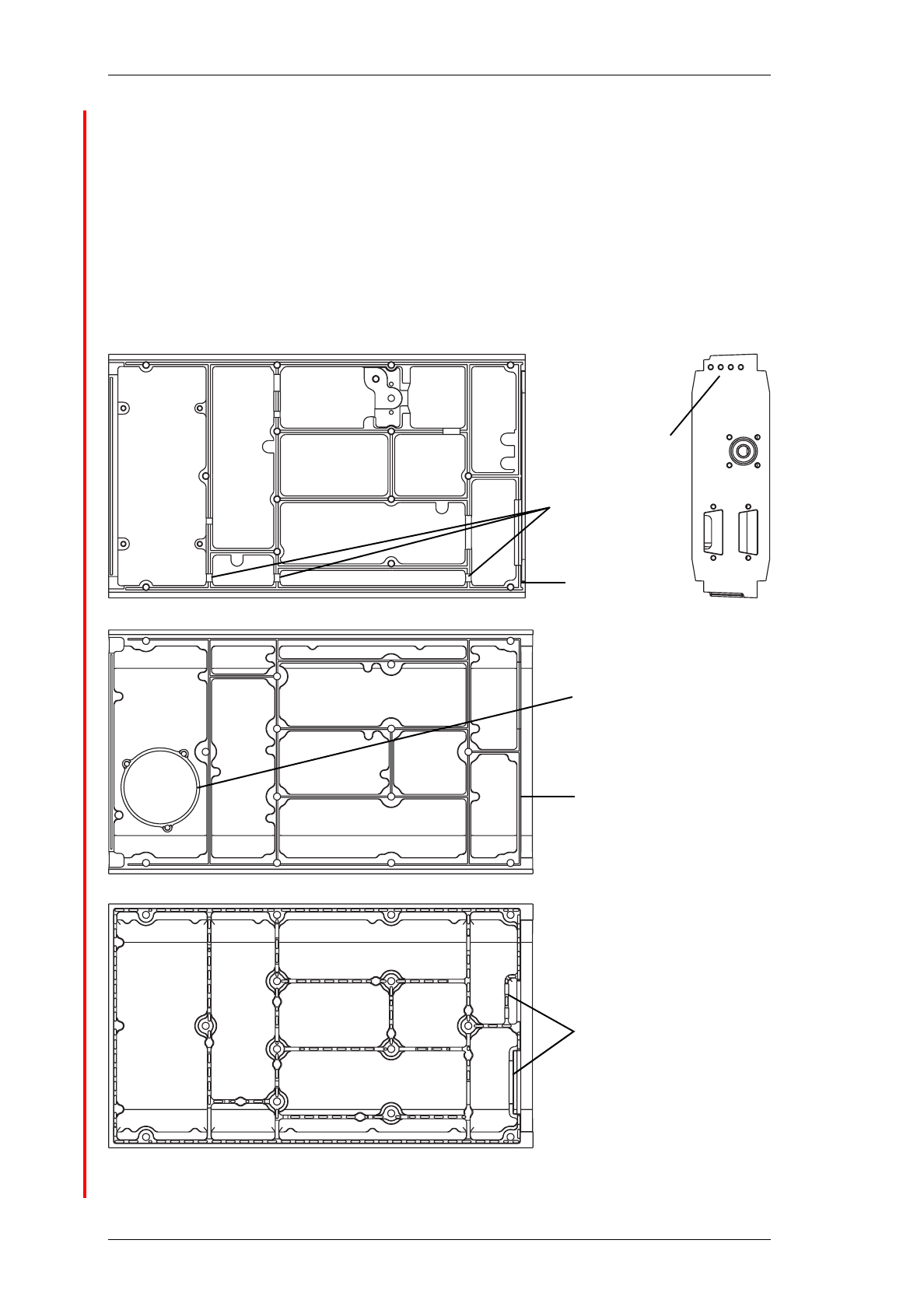
2.5 Chassis & Cover Compatibility
The chassis and covers used in T800 Series II modules incorporate a number of design
changes to improve Electro-Magnetic Compatibility (EMC) performance. It is impor-
tant that only the new-design covers are fitted to the new chassis to ensure correct
mechanical fit and continued compliance with appropriate EMC Type Approval regula-
tions.
Figure 2.3 below shows some of the main features which can be used to identify the
new-design chassis and covers.
Figure 2.3 Identification Of New-Design Chassis & Covers
Top Cover
Bottom Cover
Chassis
4 holes in
rear panel
loom channel in
top of walls
groove in top
of rear wall
ridge on top
of rear wall
provision for mounting speaker
(future development)
additional walls
←Top View Rear View→

M830-00
Component Replacement
A3.1
Copyright TEL 30/04/98
3 Component Replacement
3.1 Leaded Components
Whenever you are doing any work on the PCB that involves removing or fitting compo-
nents, you must take care not to damage the copper tracks. The two satisfactory meth-
ods of removing components from plated-through hole (PTH) PCBs are detailed below.
Note:
The first method requires the use of a desoldering station, e.g. Philips SBC
314 or Pace MBT-100E.
3.1.1 Desoldering Iron Method
Place the tip over the lead and, as the solder starts to melt, move the tip in a circu-
lar motion.
Start the suction and continue the movement until 3 or 4 circles have been com-
pleted.
Remove the tip while continuing suction to ensure that all solder is removed from
the joint, then stop the suction.
Before pulling the lead out, ensure it is not stuck to the plating.
If the lead is still not free, resolder the joint and try again.
Note:
The desoldering iron does not usually have enough heat to desolder leads
from the ground plane. Additional heat may be applied by holding a sol-
dering iron on the tip of the desoldering iron (this may require some addi-
tional help).
3.1.2 Component Cutting Method
Cut the leads on the component side of the PCB.
Heat the solder joint sufficiently to allow easy removal of the lead by drawing it
out from the component side: do not use undue force.
Fill the hole with solder and then clear with solderwick.

A3.2
Component Replacement
M830-00
23/07/99 Copyright TEL
3.2 Surface Mount Devices
Caution:
Surface mount devices (SMDs) require special storage, handling,
removal and replacement techniques. This equipment should be serv-
iced only by an approved Tait Dealer or Customer Service Organisa-
tion equipped with the necessary facilities. Repairs attempted with
incorrect equipment or by untrained personnel may result in perma-
nent damage. If in doubt, contact your nearest Tait Dealer or Customer
Service Organisation.
3.3 Cased Mica Capacitors
Cased mica capacitors can be removed by heating the top with a heavy-duty soldering
iron and gently lifting the capacitor off the PCB with a solder-resistant spike or equiva-
lent.

M830-00
Software History
A4.1
Copyright TEL 30/04/98
4 Software History
28/06/96 PGM800Win Version 1.0
18/08/97 PGM800Win Version 2.00
4.1 PGM800Win V1.0
PGM800Win V1.0 is different in concept from DOS versions of PGM800 in that it is Win-
dows1 based. It also includes many new and improved features over DOS versions of
PGM800.
The major changes are outlined below:
• The Windows environment makes data entry and editing significantly easier.
• PGM800Win includes several new radio models which are not programmable
with DOS versions of PGM800.
• Out of range frequencies will result in warning messages and will not be accepted
for entry into the standard library module. User defined modules can be created,
however, allowing variation from the standard library module.
• Channel numbers default to 0-127 to match the EPROM memory locations. How-
ever, the user can change this setting so that the channel numbers run from 1-128
to suit his/her particular needs.
Note:
The data files produced by BASEPROG V1.0 and all DOS versions of
PGM800 are still compatible with PGM800Win V1.0.
4.2 PGM800Win V2.00
PGM800Win V2.00 is an upgraded and expanded version of PGM800Win V1.0. It has
been developed specifically for T800 Series II base stations, but retains the ability to pro-
gram Series I equipment.
The major changes are outlined below:
• PGM800Win V2.0 will program T800 Series II base station modules via serial com-
munications.
• Deviation and reference modulation settings are written automatically to the
radio.
1. Windows is a registered trademark of the Microsoft Corporation.

A4.2
Software History
M830-00
30/04/98 Copyright TEL
• Extra information that is not stored in the radio (but which is still relevant to the
radio) can be saved to a file on disk (e.g. note field, auxiliary pin names, etc.).
Note:
The data files produced by BASEPROG V1.0, all DOS versions of PGM800,
and PGM800Win V1.0 are still compatible with PGM800Win V2.00.

M830-00
BI
Copyright TEL 30/04/98
Part B T835 Receiver
This part of the manual is divided into six sections, as listed below. There is a detailed
table of contents at the start of each section.
Section Title
1 General Information
2 Circuit Operation
3 Initial Tuning & Adjustment
4 Functional Testing
5 Fault Finding
6 PCB Information


M830-00
T835 General Information
B1.1
Copyright TEL 23/07/99
1 T835 General Information
This section provides a brief description of the T835 receiver, along with detailed speci-
fications and a list of types available.
The following topics are covered in this section.
Section Title Page
1.1 Introduction 1.5
1.2
1.2.1
1.2.2
1.2.3
1.2.4
1.2.4.1
1.2.4.2
1.2.4.3
1.2.5
1.2.6
1.2.6.1
1.2.6.2
1.2.6.3
Specifications
Introduction
General
RF Section
Audio Section
General
CTCSS
Mute Operation
Microcontroller
Test Standards
European Telecommunication Standard (ETS)
DTI CEPT Recommendation T/R-24-01
Telecommunications Industry Association
1.6
1.6
1.7
1.7
1.9
1.9
1.9
1.10
1.10
1.10
1.10
1.11
1.11
1.3 Product Codes 1.12
1.4 Standard Product Range 1.13
Figure Title Page
1.1
1.2
T835 Main Circuit Block Identification
T835 Front Panel Controls
1.4
1.4


M830-00
T835 General Information
B1.5
Copyright TEL 23/07/99
1.1 Introduction
The T835 is a high performance microprocessor controlled FM base station receiver
designed for single or multichannel operation in the 136 to 174MHz frequency range1.
The receiver is a dual conversion superhet with a synthesised local oscillator. The first
IF is 21.4MHz, allowing exceptionally high spurious signal rejection to be achieved in
the receiver front end. The second IF section (455kHz) combines amplitude limiting,
detection and RSSI within a single integrated circuit. This IC also drives a noise level
detector for gating the audio output. RSSI can also be used to drive a carrier mute for
audio output gating (link selectable).
The audio section output can be adjusted to deliver >+10dBm to a 600 ohm balanced
output, and 1W to a local monitor speaker. A flat or de-emphasised audio response is
link selectable.
The synthesiser frequency is programmed via the serial communications port. Eight
channel select lines are accessible via an optional D-range connector (D-range 2 -
T800-03-0000) at the rear of the set.
All components except those on the VCO board are mounted on a single PCB. This is
secured to a die-cast chassis which is divided into compartments to individually shield
each section of circuitry. Access to both sides of the main PCB is obtained by removing
each of the two chassis covers. There is provision within the chassis to mount small
option PCBs.
The front panel controls include gating sensitivity, line level, monitor volume and a
monitor mute switch.
The T835 has a width of 60mm and occupies a single space in a Tait rack frame, which
has the ability to accommodate up to seven standard modules.
1. Although capable of operating over the 136-174MHz frequency range, the T835 has a
3MHz switching range (see Section 1.2.3 and Section 3.1).
B1.6
T835 General Information
M830-00
23/07/99 Copyright TEL
1.2 Specifications
1.2.1 Introduction
The performance figures given are minimum figures, unless otherwise indicated, for
equipment tuned with the maximum switching range and operating at standard room
temperature (+22°C to +28°C) and standard test voltage (13.8V DC).
Where applicable, the test methods used to obtain the following performance figures are
those described in the EIA and ETS specifications. However, there are several parame-
ters for which performance according to the CEPT specification is given. Refer to Sec-
tion 1.2.6 for details of test standards.
Details of test methods and the conditions which apply for Type Approval testing in all
countries can be obtained from Tait Electronics Ltd.
The terms "wide bandwidth", "mid bandwidth" and "narrow bandwidth" used in this
and following sections are defined in the following table.
Sensitivity and distortion figures are stated for standard operating conditions which
includes audio de-emphasis. Note that the sensitivity and distortion figures will be
degraded when flat audio is selected.
Channel Spacing Modulation
100% Deviation Receiver
IF Bandwidth
Wide Bandwidth 25kHz ±5.0kHz 15.0kHz
Mid Bandwidth 20kHz ±4.0kHz 12.0kHz
Narrow Bandwidth 12.5kHz ±2.5kHz 7.5kHz
Link PL210 Link PL220
De-emphasised Audio 1-2 2-3
Flat Audio 2-3 1-2

M830-00
T835 General Information
B1.7
Copyright TEL 23/07/99
1.2.2 General
Number Of Channels .. 128 (standard)1
Supply Voltage:
Operating Voltage .. 10.8 to 16V DC
Standard Test Voltage .. 13.8V DC
Polarity .. negative earth only
Polarity Protection .. crowbar diode
Supply Current:
Standby .. 350mA
Full Audio .. 800mA
Operating Temperature Range .. -30°C to +60°C
Dimensions:
Height .. 183mm
Width .. 60mm
Length .. 324mm
Weight .. 2.13kg
1.2.3 RF Section
Frequency Range .. 136-174MHz
Type .. dual conversion superheterodyne
Frequency Increment .. 5 or 6.25kHz
Switching Range .. 3MHz (i.e. ±1.5MHz from the centre
frequency)
Input Impedance .. 50 ohms
Frequency Stability .. ±2.5ppm, -30°C to +60°C
(see also Section 1.4) (±1ppm available for special
applications)
Signal Strength Indicator .. -115dBm to -70dBm, 3.5 to 6.5V
(RSSI) at approx. 15dB/V
1. Additional channels may be factory programmed. Contact your nearest Tait Dealer or
Customer Service Organisation.

B1.8
T835 General Information
M830-00
23/07/99 Copyright TEL
IF Amplifiers:
Frequencies .. 21.4MHz and 455kHz
Bandwidths-
Narrow Bandwidth (NB) .. 7.5kHz
Mid Bandwidth (MB) .. 12kHz
Wide Bandwidth (WB) .. 15kHz
Sensitivity (De-emphasised Response):
Single Channel .. -117dBm
Bandspread (12dB Sinad) .. -115dBm (across switching range)
Sensitivity (Flat Response):
Single Channel .. -111dBm
Bandspread (12dB Sinad) .. -109dBm (across switching range)
Signal+Noise To Noise Ratio (Typical): De-emphasised Flat
RF Level -107dBm (CEPT) .. 30dB (WB) 25dB (WB)
25dB (NB) 20dB (NB)
RF Level -83dBm (CEPT) .. 54dB (MB) 49dB (MB)
50dB (NB) 45dB (NB)
RF Level -57dBm (EIA) .. 55dB (WB) 52dB (WB)
Selectivity:
Narrow Bandwidth (±12.5kHz) .. 86dB minimum, 89dB typical
Mid Bandwidth (±20kHz) .. 87dB minimum, 90dB typical
Wide Bandwidth (±25kHz) .. 92dB minimum, 95dB typical
Offset Selectivity (Canada only) .. 20dB
Spurious Response Attenuation .. 100dB (typical)
Intermodulation Response Attenuation:
Narrow Bandwidth .. 80dB CEPT (typical)
Mid Bandwidth .. 80dB CEPT (typical)
Wide Bandwidth .. 85dB EIA (typical)
Blocking .. 100dB
Co-channel Rejection .. 6dB
Amplitude Characteristic .. 3dB
Spurious Emissions:
Conducted .. -90dBm to 4GHz
Radiated .. -57dBm to 1GHz
-47dBm to 4GHz

M830-00
T835 General Information
B1.9
Copyright TEL 23/07/99
1.2.4 Audio Section
1.2.4.1 General
Outputs Available .. line and monitor
Frequency Response .. flat or de-emphasised (750µs)
(link selectable)
Flat Response:
Bandwidth .. 67 to 3400Hz
Response .. within +1, -2dB of output level
at 1kHz
De-emphasised Response:
Bandwidth .. 300 to 3400Hz
Response .. within +1, -3dB of a 6dB/octave
de-emphasis characteristic (ref. 1kHz)
Line Output:
Power .. adjustable to >+10dBm
Load Impedance .. 600 ohms
Distortion (@ -70dBm signal level): De-emphasised Flat
Wide Bandwidth .. ≤2% ≤2%
Mid & Narrow Bandwidth .. ≤2% ≤4%
Monitor Output:
Power .. 1W
Speaker Impedance .. 4 ohms
Distortion .. ≤3%
(@ -70dBm signal level, links set to de-emphasis)
1.2.4.2 CTCSS
Linkable High Pass Filter:
Bandwidth .. 350 to 3400Hz
Response .. within +1, -3dB of level at 1kHz
Hum And Noise .. 30dB min. at 250.3Hz
(1kHz at 60% system deviation 35dB typical (67 to 240Hz)
CTCSS at 10% system deviation)
Tone Detect:
Tone Squelch Opening .. better than 6dB sinad
3dB sinad at 250.3Hz (typical)
4dB sinad at 100Hz (typical)
Tone Detect Bandwidth .. ±2.1Hz accept (typical)
±3.0Hz reject (typical)
Response Time .. 150ms open and close (typical)

B1.10
T835 General Information
M830-00
23/07/99 Copyright TEL
1.2.4.3 Mute Operation
Systems Available .. noise mute and carrier mute
Noise Mute:
Operating Range .. 6-20dB sinad
Hysteresis .. 1.5 to 6dB
Threshold .. adjustable to -105dBm
Opening Time .. 20ms
Closing Time .. 50ms
Carrier Mute (Optional):
Operating Range .. -115 to -80dBm
Hysteresis .. 2 to 10dB
Opening Time .. 5ms
Closing Time .. 50ms
Note:
The opening and closing times given above are for the standard set-up
(SL210 linked and SL220 not linked - refer to Section 3.8).
1.2.5 Microcontroller
Auxiliary Ports:
Open Drain Type .. capable of sinking 2.25mA via 2k2Ω
Vds max. .. 5V
1.2.6 Test Standards
Where applicable, this equipment is tested in accordance with the following standards.
1.2.6.1 European Telecommunication Standard
ETS 300 086 January 1991
Radio equipment and systems; land mobile service; technical characteristics and test
conditions for radio equipment with an internal or external RF connector intended pri-
marily for analogue speech.
ETS 300 113 March 1996
Radio equipment and systems; land mobile service; technical characteristics and test
conditions for radio equipment intended for the transmission of data (and speech) and
having an antenna connector.
ETS 300 219 October 1993
Radio equipment and systems; land mobile service; technical characteristics and test
conditions for radio equipment transmitting signals to initiate a specific response in the
receiver.

M830-00
T835 General Information
B1.11
Copyright TEL 23/07/99
ETS 300 279 February 1996
Radio equipment and systems; electromagnetic compatibility (EMC) standard for pri-
vate land mobile radio (PMR) and ancillary equipment (speech and/or non-speech).
1.2.6.2 DTI CEPT Recommendation T/R-24-01
Annex I: 1988
Technical characteristics and test conditions for radio equipment in the land mobile
service intended primarily for analogue speech.
Annex II: 1988
Technical characteristics of radio equipment in the land mobile service with regard to
quality and stability of transmission.
1.2.6.3 Telecommunications Industry Association
ANSI/TIA/EIA-603-1992
Land mobile FM or PM communications equipment measurement and performance
standards.

B1.12
T835 General Information
M830-00
23/07/99 Copyright TEL
1.3 Product Codes
The three groups of digits in the T830 Series II product code provide information about
the model, type and options fitted, according to the conventions described below.
The following explanation of T830 Series II product codes is not intended to suggest that
any combination of features is necessarily available in any one product. Consult your
nearest Tait Dealer or Customer Service Organisation for more information regarding
the availability of specific models, types and options.
Model
The Model group indicates the basic function of the product, as follows:
T83X-XX-XXXX T835 receiver
T836 25W transmitter
T837 exciter
T838 50W power amplifier
T839 100W power amplifier
Type
The Type group uses two digits to indicate the basic RF configuration of the product.
The first digit in the Type group designates the frequency range:
T83X-XX-XXXX ’1’ for 136-156MHz
’2’ for 148-174MHz
The second digit in the Type group indicates the channel spacing:
T83X-XX-XXXX ’0’ for wide bandwidth (25kHz)
’3’ for mid bandwidth (20kHz)
’5’ for narrow bandwidth (12.5kHz)
Options
T83X-XX-XXXX The Options group uses four digits and/or letters to indicate
any options that may be fitted to the product. This includes
standard options and special options for specific customers.
’0000’ indicates a standard Tait product with no options fitted.
The large number of options precludes listing them here.
M830-00
T835 General Information
B1.13
Copyright TEL 23/07/99
1.4 Standard Product Range
The following table lists the range of standard T835 types (i.e. no options fitted) availa-
ble at the time this manual was published. Consult your nearest Tait Dealer or Cus-
tomer Service Organisation for more information.
You can identify the receiver type by checking the product code printed on a label on
the rear of the chassis (Figure 1.1 in Part A shows typical labels). You can further verify
the receiver type by checking the placement of an SMD resistor in the table that is screen
printed onto the PCB (refer to Section 6.1 for more details).
Frequency Range (MHz)a
a. Selectable by solder links and the appropriate VCO - refer to Sec-
tion 3.7.
136-156
IF Bandwidth (kHz) 7.5 12 15
TCXOb
b. A TCXO with a stability of ±1ppm (0°C to +60°C) is available to
suit specific requirements. Contact your nearest authorised Tait
Dealer or Customer Service Organisation for further details.
±2.5ppm -30°C to +60°C •••
Receiver Type: T835- 15-0000 13-0000 10-0000
Frequency Range (MHz)a148-174
IF Bandwidth (kHz) 7.5 12 15
TCXOb±2.5ppm -30°C to +60°C •••
Receiver Type: T835- 25-0000 23-0000 20-0000

M830-00
T835 Circuit Operation
B2.1
Copyright TEL 30/04/98
2 T835 Circuit Operation
This section provides a basic description of the circuit operation of the T835 receiver.
Note:
Unless otherwise specified, the term "PGM800Win" used in this and follow-
ing sections refers to version 2.00 and later of the software.
Refer to Section 6 where the parts lists, grid reference index and diagrams will provide
detailed information on identifying and locating components and test points on the
main PCB. The parts list and diagrams for the VCO PCB are in Part E.
The following topics are covered in this section.
Section Title Page
2.1 Introduction 2.3
2.2 Receiver Front End 2.4
2.3 Mixer 2.5
2.4 IF Circuitry 2.5
2.5 Noise Mute (Squelch) 2.6
2.6 Carrier Mute 2.6
2.7 Audio Processor 2.7
2.8 Power Supply And Regulators 2.8
2.9 Microcontroller 2.9
2.10 Synthesised Local Oscillator 2.10
2.11 VCO 2.11
2.12 Received Signal Strength Indicator (RSSI) 2.11
Figure Title Page
2.1
2.2
2.3
2.4
2.5
2.6
T835 High Level Block Diagram
T835 Front End, IF and Mute Block Diagram
T835 Audio Processor Block Diagram
T835 Power Supply And Regulator Block Diagram
T835 Microcontroller Block Diagram
T835 Synthesiser Block Diagram
2.3
2.4
2.7
2.8
2.9
2.10

M830-00
T835 Circuit Operation
B2.3
Copyright TEL 30/04/98
2.1 Introduction
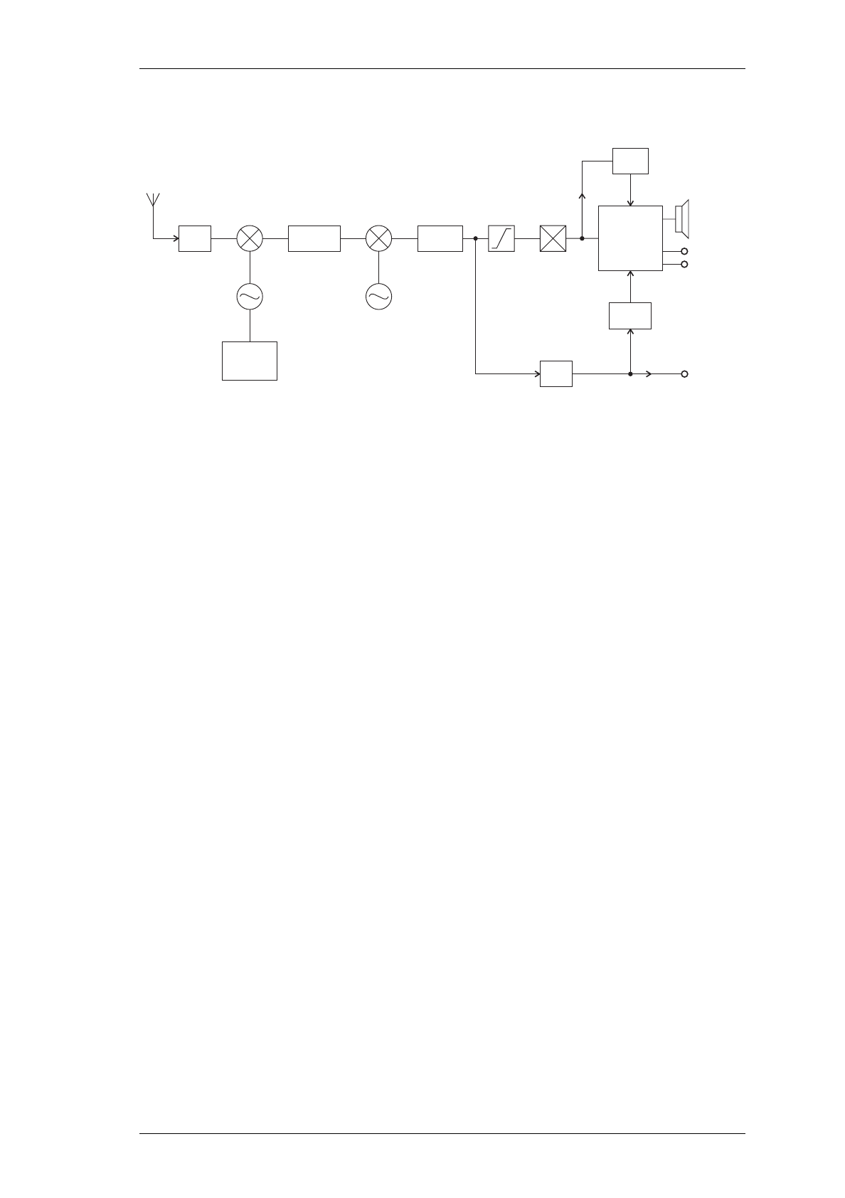
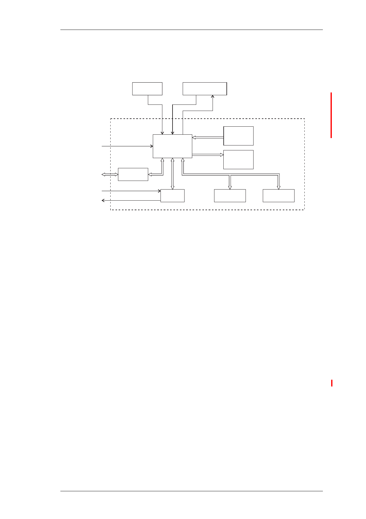
Figure 2.1 T835 High Level Block Diagram
The T835 receiver consists of a number of distinct stages:
• front end
•mixer
• synthesised local oscillator
•IF
• audio processor
• mute (squelch)
• regulator circuits
• received signal strength indicator (RSSI).
These stages are clearly identifiable in Figure 2.1. Refer to the circuit diagrams in Sec-
tion 6 for further detail.
21.4MHz
IF 455kHz
IF
Carrier
Mute
RSSI
Noise
Mute
Front
End
12.8MHz
Master
Oscillator
Audio
Processor
Mixer Mixer Limiter
FM
Detector
Synthesised
Local
Oscillator
Second
Local
Oscillator
Speaker
}
600Ω
Line
B2.4
T835 Circuit Operation
M830-00
23/07/99 Copyright TEL
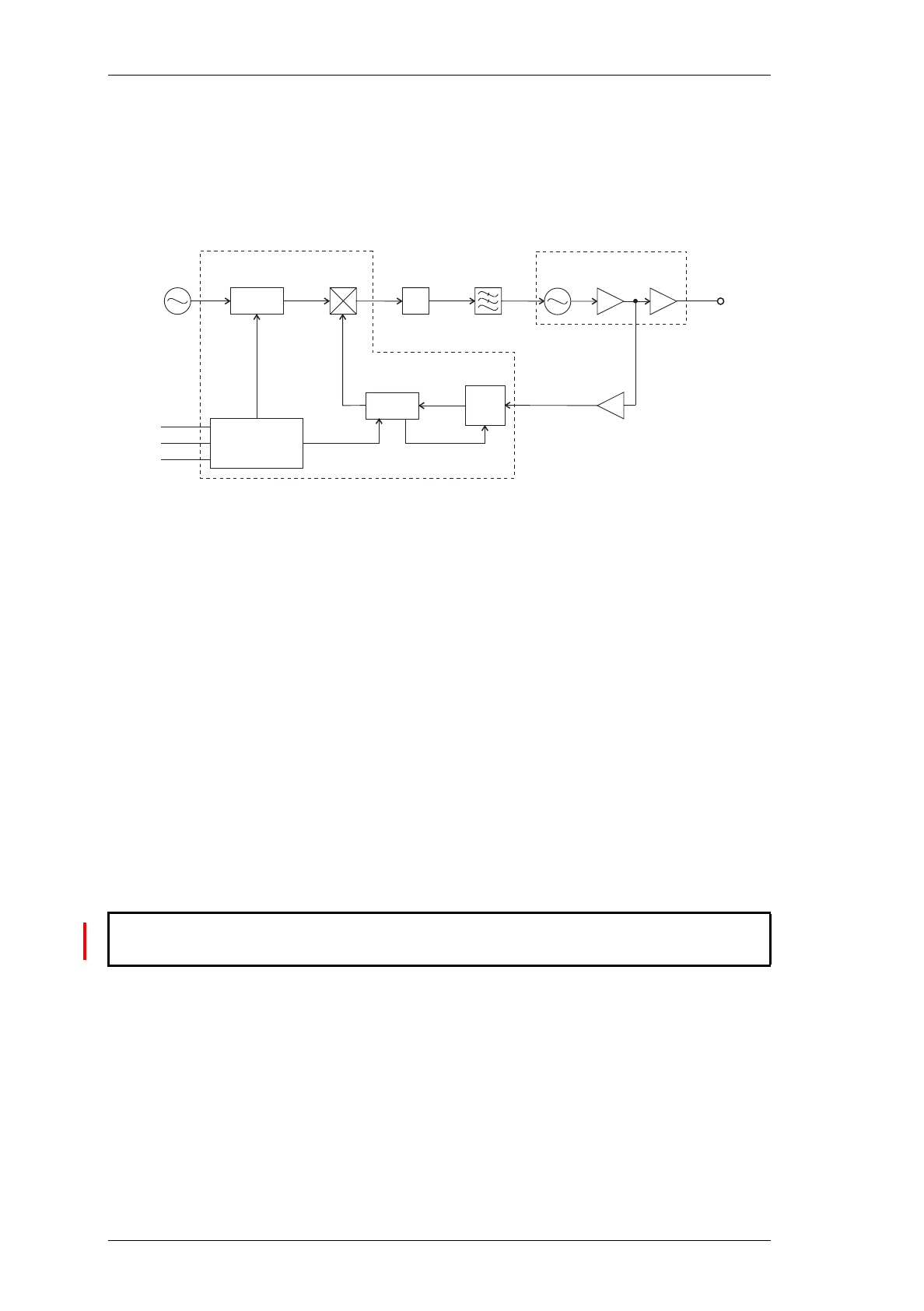
2.2 Receiver Front End
(Refer to the front end, IF section and audio processor circuit diagrams (sheets 4, 3 and 2
respectively) in Section 6.)
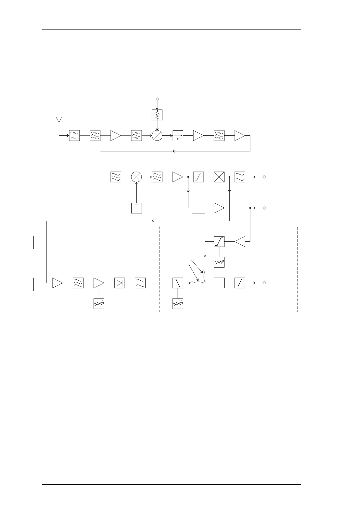
Figure 2.2 T835 Front End, IF and Mute Block Diagram
The incoming signal from the N-type antenna socket is fed through a 7-pole, low pass
filter with a cut frequency of approximately 200MHz. This low loss filter (typically less
than 0.5dB insertion loss over 136-174MHz) provides excellent immunity to interference
from high frequency signals.
The signal is then further filtered, using a notched doublet (L410, L420) which provides
exceptional image rejection, before being amplified by approximately 12dB (Q420). The
signal is then passed through a further doublet (L460, L470) before being presented to
the mixer.
Each sub-block within the front end has been designed with 50 ohm terminations for
ease of testing and fault finding.
t∆
Mixer
2-Pole
Crystal
Filter
Buffer
Amp
RSSI
Comparator
RF In
136-174MHz
Harmonic
Filter Doublet
Filter Doublet
Filter
RF
Amp
Local Oscillator
(From Synthesiser)
Diplexer
Post
Mixer
Amp
4-Pole
Crystal
Filter IF
Amp
2dB Pad
21.4MHz
Mixer
(NE612) Ceramic
Filter IF
Amp Limiter
(NE614)
FM
Detector
(NE614)
Low
Pass
Filter
21.4MHz 455kHz
2nd LO
20.945MHz
Amp Active
Filter LF
Amp Diode
Detector
Smoothing
Filter
Gain
Adjust
Noise
Mute
Adjust
Gating
Delays Comparator
Comparator
Carrier
Mute
Adjust
Carrier Mute
Noise Mute
Buffer Amp
Rx Gate Out
(To Audio
Processor)
Audio Section
Link:
RSSI Output
Voltage
(To D-Range
Socket)
Audio
(To Audio
Processor)

M830-00
T835 Circuit Operation
B2.5
Copyright TEL 30/04/98
2.3 Mixer
(Refer to the front end circuit diagram (sheet 4) in Section 6 and Figure 2.2.)
IC410 is a high level mixer requiring a local oscillator (LO) drive level of +17dBm (nom-
inal). The voltage controlled oscillator (VCO) generates a level of +22dBm (typical) and
this is fed to the mixer via a 2dB attenuator pad. A diplexer terminates the IF port of the
mixer in a good 50 ohms, thus preventing unnecessary intermodulation distortion.
2.4 IF Circuitry
(Refer to the IF section circuit diagram (sheet 3) in Section 6 and Figure 2.2.)
Losses in the mixer are made up for in a tuned, common gate, post mixer amplifier
(Q310). Several stages of amplification and filtering are employed in the IF circuitry.
The first crystal filter is a 4-pole device (&XF310 and &XF320) which is matched into 50
ohms on both its input and output ports. This stage is followed by a two-stage amplifier
(designed as a 50 ohm block) and second crystal filter (2 pole, &XF330), after which the
signal is mixed down to 455kHz with the second local oscillator (20.945MHz) by IC340.
The 455kHz signal is filtered using a six-pole ceramic filter (&XF340) before being lim-
ited and detected.
The second IF mixer, limiter, detector and RSSI is in a 16-pin IC (IC350). Quadrature
detection is employed, using L360, and the recovered audio on pin 7 of IC350 is typi-
cally 0.3V p-p for 60% system deviation.

B2.6
T835 Circuit Operation
M830-00
30/04/98 Copyright TEL
2.5 Noise Mute (Squelch)
(Refer to the audio processor and IF section circuit diagrams (sheets 2 and 3 respec-
tively) in Section 6 and Figure 2.2.)
The noise mute operates on the detected noise outside the audio bandwidth. An opera-
tional amplifier in IC390 is used as an active band pass filter centred on 70kHz to filter
out audio components. The noise spectrum is then further amplified in a variable gain,
two-stage amplifier (Q340 & Q350) with additional filtering. The noise is then rectified
(D310) and filtered to produce a DC voltage proportional to the noise amplitude. The
lowest average DC voltage corresponds to a high RF signal strength and the highest DC
voltage corresponds to no signal at the RF input.
The rectified noise voltage is compared with a threshold voltage set up on RV230, the
front panel "Gating Sensitivity" potentiometer. Hysteresis is introduced by the feedback
resistor (R267) to prevent the received message from being chopped when the average
noise voltage is close to the threshold. R281 and R280 determine the mute opening and
closing times and, in combination with solder links SL210 and SL220, provide three time
delay options (SL210 is linked as standard - refer to Section 3.8). The mute control sig-
nal at pin 7 of IC270 is used to disable the speaker and line audio outputs. The speaker
output can be separately enabled for test purposes by operating the front panel mute
disable switch, SW201.
2.6 Carrier Mute
(Refer to the audio processor and IF section circuit diagrams (sheets 2 and 3 respec-
tively) in Section 6 and Figure 2.2.)
A high level carrier mute facility is also available. The RSSI (refer to Section 2.12) pro-
vides a DC voltage proportional to the signal strength. This voltage is compared with a
preset level, set up on RV235, and may be linked into the mute timing circuit using
PL250. PL250 selects either the noise mute or the carrier mute. From this point both the
noise and carrier mute circuits operate in the same manner, using common circuitry.
M830-00
T835 Circuit Operation
B2.7
Copyright TEL 30/04/98
2.7 Audio Processor
(Refer to the audio processor circuit diagram (sheet 2) in Section 6.)
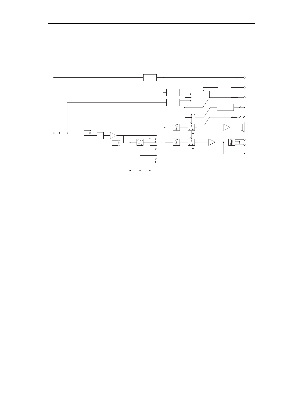
Figure 2.3 T835 Audio Processor Block Diagram
The recovered audio on pin 7 of IC350 is processed by IC390 and passed through a fre-
quency compensation network and a third order elliptic active filter (IC210) to give the
required response. Linking (PL220 & PL210) is available to give either a flat or
de-emphasised audio response, with de-emphasis giving a 6dB/octave roll off. The out-
put of IC210 is split to provide separate paths for the speaker and line outputs. The
"Audio 1", Audio 2" and "Speech" lines allow access to the receiver’s audio path for
external signalling purposes (refer to Section 3.5).
The signals are passed to audio drive amplifiers IC240 and IC260. Under muted condi-
tions the inputs of these amplifiers are shunted to ground via transistors Q230 and Q290
respectively. The audio output of IC240 has a DC component which is removed by
C249, and this then drives a speaker directly. The output of IC260 is fed into a line trans-
former to provide a balanced 2-wire or 4-wire, 600 ohm output.
The speaker volume is set using the front panel "Monitor Volume" knob (RV205) and the
line level is set using the recessed "Line Level" potentiometer (RV210).
The red front panel "Gate" LED (D250) indicates the status of the mute circuit. When a
signal above the mute threshold is received, the LED is illuminated. The "Monitor
Mute" switch (SW201) on the front panel opens the mute, allowing continuous monitor-
ing of the audio signal (on = audio muted; off = audio unmuted).
The mute control line is available on pad 234 ("RX GATE OUT") for control of external
circuitry. A high (9V) on pad 234 indicates that the audio is disabled and a low (0V)
indicates that a signal above the mute threshold level is being received.
From
IF Stage
Demodulated
Signal
(*IF Audio
Compensation
Circuit)
Driver Amp
Line Output
12V
Relay
Speech
Audio 1
Output Audio 2
Input
High Pass
Filter
Speaker
Mute
Line
Mute
Carrier
Mute
RSSI
(Optional)
Rx Disable
Timer
Noise
Mute
PL260
PL250
PL270
RSSI Output
Mute Relay
Gate Output
Rx Disable
(Optional Pad)
Mute Disable
Speaker Output
Line Monitor
12
1
2
2
1
3
1
5
2
2
3
3
4
1
PL240
PL230
Driver Amp
Flat/De-
emphasis
LPF
PL210
2
3
Flat/De-
emphasis
Amplifier
PL220
1
23
*IF
Comp
Monitor
Volume
Line
Level
B2.8
T835 Circuit Operation
M830-00
23/07/99 Copyright TEL
The audio can also be disabled using the "RX-DISABLE" inputs, pads 225 or 228, having
connected the "RX-DISABLE" link between pins 1 & 2 of PL260. An adjustable time
delay (RV220) is provided on these lines. In order to disable the audio, either pad must
be pulled to 0V (refer to Section 1.4 in Part G).
An undedicated relay is provided (RL210) for transmitter keying or other functions and
this can be operated from the mute line by linking PL270.
2.8 Power Supply And Regulators
(Refer to the regulators circuit diagram (sheet 6) in Section 6.)
Figure 2.4 T835 Power Supply And Regulators Block Diagram
The T835 is designed to operate off a 10.8-16V DC supply (13.8V nominal). A 5.3V regu-
lator (IC630) runs directly from the 13.8V rail, driving much of the synthesiser circuitry.
It is also used as the reference for a DC amplifier (IC640, Q630 & Q620) which provides
a medium current capability 9V supply.
A switching power supply, based on Q670 and Q660, runs off the 9V supply and pro-
vides a low current capability +20V supply. This is used to drive the synthesiser loop
filter (IC740), giving a VCO control voltage of up to 20V.
The 13.8V supply drives both output audio amplifiers without additional regulation. A
separate 5V regulator (IC610) drives the microprocessor and associated digital circuitry.
The output of this regulator is monitored by the Low Voltage Interrupt (LVI) circuit
(IC650).
A crowbar diode is fitted for protection against connection to a power supply of incor-
rect polarity. It also provides transient overvoltage protection.
Note:
A fuse must be fitted in the power supply line for the diode to provide effec-
tive protection.
LVI
LVI
5V
Reg
DC
Amp Switching
PS 5V Dig
Reg µP
Reset
13.8V
Nom. 5V 5V Dig9V 20V
13.8V Nom.
From Rear
D-Range 1
Crowbar
Diode
M830-00
T835 Circuit Operation
B2.9
Copyright TEL 23/07/99
2.9 Microcontroller
(Refer to the microcontroller circuit diagram (sheet 8) in Section 6.)
Figure 2.5 T835 Microcontroller Block Diagram
Overall system control of the T835 is accomplished by the use of a member of the 80C51
family of microcontrollers (IC810) which runs from internal ROM and RAM. Four ports
are available for input/output functions.
Non-volatile data storage is achieved by serial communication with a 16kBit EEPROM
(IC820). This serial bus is also used by the microcontroller to program the synthesiser
(IC740).
The main tasks of the microcontroller are as follows:
• program the synthesiser;
• interface with the PGM800Win programming software at 9600 baud via the
serial communication lines on D-range 1 (PL100) & D-range 2;
• monitor channel change inputs from D-range 2;
• generate timing waveforms for CTCSS detection;
• coordinate and implement timing control of the receiver;
• control the front panel "Supply" LED (refer to Section 5.3).
Channel
Select
Port
Auxiliary
Output
Port
Microcontroller
12.8MHz
Clock
Microcontroller Cavity
Audio In
Speech
External
Serial
Port
EEPROM Synthesiser
CTCSS
Decoder
Converter
5V Reset
5V Digital
Regulator Watchdog Timer
& LVI
Watchdog
B2.10
T835 Circuit Operation
M830-00
23/07/99 Copyright TEL
2.10 Synthesised Local Oscillator
(Refer to the synthesiser circuit diagram (sheet 7) in Section 6 and the VCO circuit dia-
gram in Part E.)
Figure 2.6 T835 Synthesiser Block Diagram
The synthesiser (IC740) employs a phase-locked loop (PLL) to lock a voltage controlled
oscillator (VCO) to a given reference frequency. The synthesiser receives the divider
information from the control microprocessor via a 3-wire serial bus (clock, data, enable).
When the data has been latched in, the synthesiser processes the incoming signals from
the VCO buffer (fin) and the reference oscillator (fref).
A reference oscillator at 12.8MHz (IC700) is buffered (IC710) and divided down to
6.25kHz or 5kHz within the synthesiser IC (IC740).
A buffered output of the VCO is divided with a prescaler and programmable divider
which is incorporated into the synthesiser chip (IC740). This signal is compared with
the reference signal at the phase detector (also part of the synthesiser chip). The phase
detector outputs drive a balanced charge pump circuit (Q760, Q770, Q775, Q780, Q785)
and active loop filter (IC750, Q790) which produces a DC voltage between 0V and 20V
to tune the VCO. This VCO control line is further filtered (R510, C505) to attenuate
noise and other spurious signals. Note that the VCO frequency increases with increas-
ing control voltage.
Editor’s Note:
The last paragraph in Section 2.10 has been deleted as it applied
only to an exciter/transmitter.
12.8MHz
Reference
Oscillator
Serial
Bus
/R
Reference
Divider Phase
Detector Charge
Pump Loop
Filter
VCO PCB
FREQUENCY SYNTHESISER IC
VCO Buffer Output
Buffer
+22dBm
L.O.
Clk
Data
En Controller Buffer
fin
fref
/N
Programmable
Divider
64/65
Prescaler

M830-00
T835 Circuit Operation
B2.11
Copyright TEL 23/07/99
2.11 VCO
(Refer to the VCO circuit diagram in Part E.)
The VCO transistor (Q1) operates in a common source configuration, with an LC tank
circuit coupled between its gate and drain to provide the feedback necessary for oscilla-
tion. The VCO control voltage from the loop filter (IC750) is applied to the varicaps
(D1-D4) to facilitate tuning within a 3MHz band of frequencies. A trimcap (CV1) is
used for coarse tuning of the VCO. The output from the oscillator circuit drives a cas-
code amplifier stage (Q2, Q3) which supplies +10dBm (typically) to a further stage of
amplification, Q5. This is the final amplifier on the VCO PCB, and delivers +22dBm
(typically) to the receiver mixer input pad.
A low level "sniff" is taken from the input to Q5 and used to drive the divider buffer for
the synthesiser (IC740).
The VCO operates at the actual frequency required by the first mixer, i.e. there are no
multiplier stages.
The VCO frequency spans from either 157-177MHz or 169-196MHz according to prod-
uct type (refer to Section 1.4). The VCO is tuned to 21.4MHz above the desired receive
frequency (high side injection) to produce a 21.4MHz IF signal at the output of the
mixer.
2.12 Received Signal Strength Indicator (RSSI)
(Refer to the IF section circuit diagram (sheet 3) in Section 6.)
The RSSI provides a DC voltage proportional to the signal level at the receiver input and
is an on-chip function of IC350. Buffering is provided by IC390 and the voltage is avail-
able at D-range 1 (PL100 pin 5).
The RSSI also provides the capability for high level signal strength muting, which may
be selected on PL250 (refer to Section 3.5). The mute threshold may be set between
-115dBm and -70dBm at RV235.


M830-00
T835 Initial Tuning & Adjustment
B3.1
Copyright TEL 23/07/99
3 T835 Initial Tuning & Adjustment
Caution:
This equipment contains CMOS devices which are susceptible to dam-
age from static charges. Refer to Section 1.2 in Part A for more infor-
mation on anti-static procedures when handling these devices.
The following section describes both short and full tuning and adjustment procedures
and provides information on:
• channel programming
• selecting the required audio links
• synthesiser alignment
• receiver front end and IF alignment
• noise and carrier level mute adjustment
• setting the line and monitor output levels
• setting up the RSSI.
Note:
Unless otherwise specified, the term "PGM800Win" used in this and follow-
ing sections refers to version 2.00 and later of the software.
Refer to Figure 4.3 which shows the location of the main tuning and adjustment con-
trols. Refer also to Section 6 where the parts lists, grid reference index and diagrams
will provide detailed information on identifying and locating components and test
points on the main PCB. The parts list and diagrams for the VCO PCB are in Part E.
Section Title Page
3.1 Introduction 3.3
3.2 Channel Programming 3.3
3.3 Test Equipment Required 3.4
3.4
3.4.1
3.4.2
3.4.3
3.4.4
3.4.4.1
3.4.4.2
3.4.5
3.4.6
3.4.6.1
3.4.6.2
3.4.6.3
3.4.7
Short Tuning Procedure
Introduction
Synthesiser Alignment
Front End Alignment
Mute Adjustment
Noise Mute
Carrier Level Mute
Line Amplifier Output
CTCSS
Decoder Operation
Opening Sinad
High Pass Filter
RSSI (If Used)
3.5
3.5
3.5
3.5
3.6
3.6
3.6
3.6
3.7
3.7
3.7
3.7
3.8

B3.2
T835 Initial Tuning & Adjustment
M830-00
23/07/99 Copyright TEL
3.5
3.5.1
3.5.2
Audio Processor Links
General
Audio Processor Linking Details For CTCSS
3.8
3.8
3.9
3.6 Synthesiser Alignment 3.10
3.7 Alignment Of Receiver Front End And IF 3.10
3.8 Gating Delay 3.12
3.9 Noise Mute Adjustment 3.12
3.10 Carrier Level Mute 3.12
3.11
3.11.1
3.11.2
Audio Processor
Line Amplifier Output
Monitor Amplifier Output (Speaker Output)
3.13
3.13
3.13
3.12
3.12.1
3.12.2
3.12.3
CTCSS
Decoder Operation
Opening Sinad
High Pass Filter
3.13
3.13
3.13
3.14
3.13 RSSI 3.14
Figure Title Page
3.1
3.2
T835 Test Equipment Set-up For Short Tuning Procedure
T835 Test Equipment Set-up For Full Tuning & Adjustment
Procedure
3.4
3.4
Section Title Page

M830-00
T835 Initial Tuning & Adjustment
B3.3
Copyright TEL 23/07/99
3.1 Introduction
When you receive your T835 receiver it will be run up and working on a particular fre-
quency (the "default channel")1. If you want to switch to a frequency that is within the
3MHz switching range (i.e. ±1.5MHz from the factory programmed frequency), you
should only need to reprogram the receiver with the PGM800Win software (refer to the
PGM800Win programming kit and Section 3.2 below).
However, if you want to switch to a frequency outside the 3MHz switching range, you
will have to reprogram and re-tune the receiver to ensure correct operation. In this case
you should carry out the short tuning procedure described in Section 3.4.
If you have carried out repairs or other major adjustments, you must carry out the full
tuning and adjustment procedure described in this section (except for Section 3.4).
3.2 Channel Programming
You can program up to 128 channel frequencies into the receiver’s EEPROM memory
(IC820) by using the PGM800Win software package and an IBM PC. You can also use
PGM800Win to select the receiver’s current operating frequency (or "default channel").
If the receiver is installed in a rack frame, you can program it via the programming port
in the speaker panel. However, you can also program the receiver before it is installed
in a rack frame as follows:
• by using a T800-01-0010 calibration test unit;
• via D-range 1;
• via D-range 2 (standard T800-03-0000 auxiliary D-range only);
• via SK805 (internal Micromatch connector).
If you do not use the T800-01-0010, you will have to connect the PC to the receiver via a
module programming interface (such as the T800-01-0004).
For a full description of the channel programming procedure, refer to the PGM800Win
programming software user’s manual.
Note:
When an auxiliary D-range kit (D-range 2 - T800-03-0000) is fitted, you can
also select a channel with an external switch, such as the DIP switch on the
rack frame backplane PCB. Refer to Part C in the T800 Series Ancillary
Equipment Service Manual (M800-00-101 or later issue) or consult your
nearest Tait Dealer or Customer Service Organisation for further details.
1. Use the "Read Module" function in PGM800Win to find out what the default channel is.
B3.4
T835 Initial Tuning & Adjustment
M830-00
30/04/98 Copyright TEL
3.3 Test Equipment Required
You will need the following test equipment:
• computer with PGM800Win installed
• T800 programming kit
• module programming interface (e.g. T800-01-0004 - optional)
• 13.8V power supply
• digital multimeter
• audio signal generator
• RF signal generator
• audio voltmeter
• sinad meter
• oscilloscope
• distortion meter
• T800-01-0010 calibration test unit (optional)
•4Ω speaker (not needed if the calibration test unit is used)
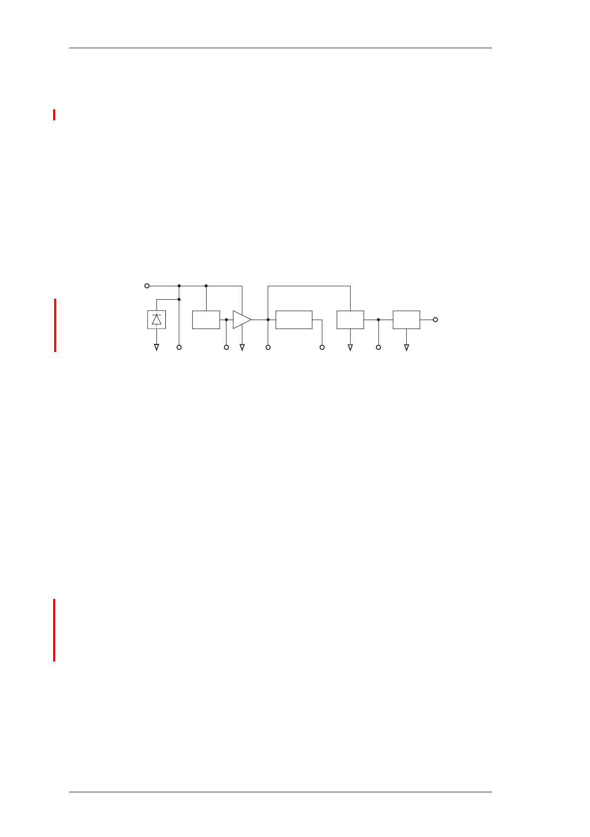
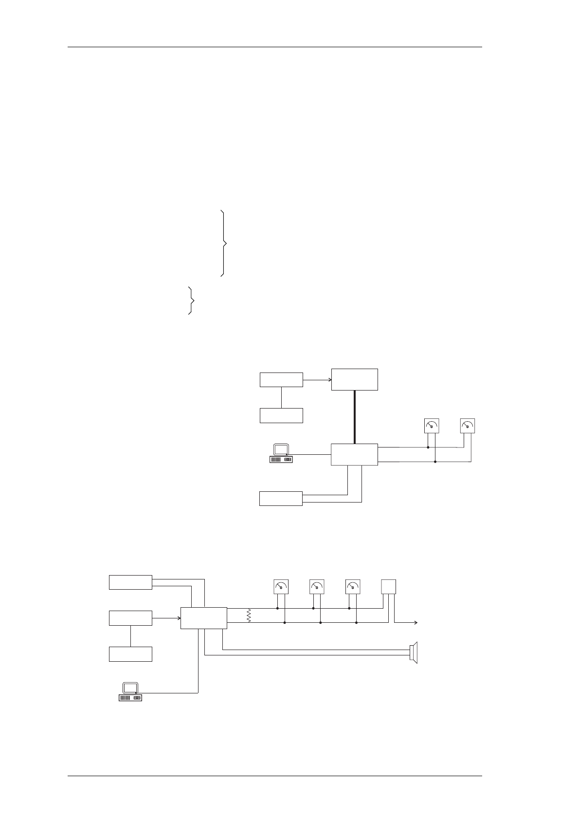
Figure 3.1 T835 Test Equipment Set-up For Short Tuning Procedure
Figure 3.2 T835 Test Equipment Set-up For Full Tuning & Adjustment Procedure
or RF test set (optional)
not needed for short tuning procedure
Receiver
RF In
RF Signal
Generator
Audio Signal
Generator
PSU
+13.8V
-Ve
External
Modulation Sinad
Meter Audio
Voltmeter
Line
Line
T800
Calibration
Test Unit
PGM800Win
Figure 3.1 and Figure 3.2 show
typical test equipment set-ups
(with and without a T800-01-0010
calibration test unit).
Receiver
RF In
RF Signal
Generator
Audio Signal
Generator
PSU
+13.8V
-Ve
External
Modulation GND
Distortion
Meter Sinad
Meter Audio
Voltmeter Oscilloscope
Line
Line 600Ω
Speaker
Output
Probe
4ΩSpeaker
(Or 4ΩResistor)
CH1
CH2
GND
PGM800Win
Serial
Com
via module programming interface
(e.g. T800-01-0004)

M830-00
T835 Initial Tuning & Adjustment
B3.5
Copyright TEL 23/07/99
3.4 Short Tuning Procedure
Use this procedure only if you want to reprogram the receiver to a frequency outside the
3MHz switching range and do not intend to carry out any other major adjustments or
repairs.
3.4.1 Introduction
Reprogram the operating frequency as described in the PGM800Win program-
ming kit (refer to Section 3.2).
Remove the top cover (nearest the handle).
Set up the test equipment as described in Section 3.3.
Set the links in the audio processor section as required (refer to Section 3.5).
3.4.2 Synthesiser Alignment
• Connect a high impedance voltmeter to PL4-1 or the junction of L1 & R1 in the
VCO (this measures the synthesiser loop voltage).
•Single Channel Tune VCO trimmer CV1 for a synthesiser loop voltage of
9V.
Multichannel Tune VCO trimmer CV1 for a synthesiser loop voltage of
9V on the middle channel.
If there is no middle channel, tune CV1 so that the chan-
nels are symmetrically placed around a loop voltage of 9V.
All channels should lie within the upper and lower limits
of 13V and 5V respectively.
Do not attempt to program channels with a greater fre-
quency separation than the specified switching range of
3MHz.
3.4.3 Front End Alignment
Note 1:
In this and following sections deviation settings are given first for wide
bandwidth sets, followed by settings in brackets for mid bandwidth sets ( )
and narrow bandwidth sets [ ].
Note 2:
For multichannel operation align the receiver on a frequency in the middle
of the required band.
Set RV230 (front panel gating sensitivity) fully clockwise.
Inject a strong on-channel RF signal with ±3kHz deviation (±2.4kHz) [±1.5kHz] at

B3.6
T835 Initial Tuning & Adjustment
M830-00
23/07/99 Copyright TEL
1kHz into the antenna socket and adjust front end doublets L410, L420, L460 &
L470 to give best sinad.
Continually decrease the RF level to maintain 12dB sinad.
Readjust L410, L420, L460 & L470 to give best sinad.
With PL210 and PL220 connected for de-emphasised audio response, the receiver
sensitivity should be better than -117dBm, assuming that the audio levels are not
being overdriven (refer to Section 3.4.5).
3.4.4 Mute Adjustment
Carry out the one of the following sets of instructions according to the mute option you
have selected.
3.4.4.1 Noise Mute
Connect pins 1 & 2 of PL250 to enable the noise mute.
Set the RF level to -105dBm with ±3kHz deviation (±2.4kHz) [±1.5kHz] at 1kHz.
Set RV230 (front panel gating sensitivity) fully anticlockwise.
Adjust RV330 (noise mute gain) fully clockwise to close the mute (if necessary
turn off the RF signal and then turn it on again).
Rotate RV330 anticlockwise until the mute just opens.
Reset the signal generator for the required opening sinad and adjust RV230 clock-
wise until the mute just opens.
3.4.4.2 Carrier Level Mute
Connect pins 2 & 3 of PL250 to enable the carrier mute and disable the noise mute.
Apply an on-channel signal from the RF generator at the required mute opening
level with ±3kHz deviation (±2.4kHz) [±1.5kHz] at 1kHz.
Adjust RV235 (carrier mute) anticlockwise to close the mute (if necessary, momen-
tarily turn off the RF), then slowly adjust it clockwise until the mute just opens.
The mute should now open at this preset level.
3.4.5 Line Amplifier Output
Apply an on-channel signal from the RF generator at a level of -70dBm with
±3kHz deviation (±2.4kHz) [±1.5kHz] at 1kHz.
Adjust RV210 (front panel line level) to set the line level to the required output
level.

M830-00
T835 Initial Tuning & Adjustment
B3.7
Copyright TEL 23/07/99
3.4.6 CTCSS
3.4.6.1 Decoder Operation
Program a CTCSS tone on the set channel using PGM800Win.
Set the RF signal generator output to -70dBm.
Modulate the generator with both:
• a 1kHz tone at ±3kHz deviation (±2.4kHz) [±1.5kHz];
• and a CTCSS tone at the programmed frequency at ±500Hz deviation (±400Hz)
[±300Hz].
Check that the receiver gate opens and the front panel "Gate" LED is on.
3.4.6.2 Opening Sinad
Adjust RV230 (front panel gating sensitivity) fully clockwise.
Reduce the RF signal level to -110dBm.
Observe the sinad meter and reduce the RF level until the receiver mute closes.
Slowly increase the signal level until the receiver mute just opens and stays open.
With PL240 pins 1 & 2 linked (high pass filter bypassed), check that the sinad is
less than 6dB.
Reset the signal generator for the required opening sinad, adjust RV230 fully anti-
clockwise, then clockwise until the mute just opens.
3.4.6.3 High Pass Filter
Set the audio processor links as follows:
Reset the RF signal generator output to -70dBm and note the line level (measure-
ment A).
Reduce the 1kHz generator to zero output and measure the line level again (meas-
urement B).
Check that measurement B is at least 30dB below measurement A.
Plug Link Function
PL210 1 - 2 de-emphasised response
PL230 2 - 3 audio from internal CTCSS speech filter
PL240 4 - 5 audio input via PL230 or I/O pad

B3.8
T835 Initial Tuning & Adjustment
M830-00
23/07/99 Copyright TEL
3.4.7 RSSI (If Used)
Align the receiver as instructed in Section 3.6 and Section 3.7.
Apply an on-channel signal from the RF generator at a level of -100dBm with
±3kHz deviation (±2.4kHz) [±1.5kHz] at 1kHz.
Adjust RV320 (RSSI level) to give 4.5V RSSI output on pin 5 of D-range 1 (PL100)
when measured with a high impedance DMM.
3.5 Audio Processor Links
3.5.1 General
Use the following table to set up the audio processor to the configuration you require.
You should set the audio processor links before carrying out the receiver alignment.
The factory settings are shown in brackets [ ].
Plug Link Function
PL210 [1 - 2]
2 - 3 de-emphasised response
flat response
PL220 1 - 2
[2 - 3] flat response
de-emphasised response
PL230a
a. Refer to Section 3.5.2 for further details.
1 - 2
[2 - 3]
3 - 4
audio input via AUDIO-2 pad
audio from internal CTCSS speech filter
audio input via I/O pad P250
PL240a
1 - 2
[2 - 3]
or
3 - 4
4 - 5
bypass high pass filter
300Hz high pass filter in circuit
audio input via PL230 or I/O pad
PL250 [1 - 2]
2 - 3 noise mute
carrier mute
PL260b
b. Refer to Section 1.4 in Part G for further details.
1 - 2
[2 - 3] RX-DISABLE link
not connected
PL270 [1 - 2]
2 - 3 relay link
not connected

M830-00
T835 Initial Tuning & Adjustment
B3.9
Copyright TEL 30/04/98
3.5.2 Audio Processor Linking Details For CTCSS
You must connect the audio processor links correctly according to the CTCSS option
used, as shown in the table below.
The conditions stated in the above table are defined as follows:
• standard, no CTCSS - no CTCSS or other sub-audio signalling used
- audio bandwidth 300Hz to 3kHz
- hum & noise -55dB
• received CTCSS tone - tone and speech transmitted down 600 ohm line
+ speech to line output - audio bandwidth 10Hz to 3kHz
- hum & noise -45dB
• high pass filtered speech - 400Hz to 3kHz
+ internal CTCSS detection - hum & noise -30dB with 250.3Hz tone present
• external CTCSS detection - decoding performed through the receiver (but
externally)
- speech injected back into receiver via "AUDIO-2"
and sent down 600 ohm line
Note 1:
AUDIO-2 is available on D-range 1 (PL100) pin 7 via the link resistor R160.
Although PL100 pin 7 is already assigned to SERIAL-COM, this can be disa-
bled by removing R808.
Note 2:
External CTCSS units can connect in series with the audio chain via
AUDIO-1 and AUDIO-2.
CTCSS Option PL230 PL240
standard, no CTCSS 2 - 3 2 - 3
received CTCSS + speech
passed to line output 3 - 4 1 - 2
high pass filtered speech,
internal CTCSS detection 2 - 3 4 - 5
external CTCSS detection 1 - 2 4 - 5

B3.10
T835 Initial Tuning & Adjustment
M830-00
23/07/99 Copyright TEL
3.6 Synthesiser Alignment
• Ensure that the receiver has been programmed with the required frequencies
using PGM800Win software.
• Connect a high impedance voltmeter to PL4-1 or the junction of L1 & R1 in the
VCO (this measures the synthesiser loop voltage).
•Single Channel Tune VCO trimmer CV1 for a synthesiser loop voltage of
9V.
Multichannel Tune VCO trimmer CV1 for a synthesiser loop voltage of
9V on the middle channel.
If there is no middle channel, tune CV1 so that the chan-
nels are symmetrically placed around a loop voltage of 9V.
All channels should lie within the upper and lower limits
of 13V and 5V respectively.
Do not attempt to program channels with a greater fre-
quency separation than the specified switching range of
3MHz.
• The TCXO (IC700) output frequency should be trimmed when the IF is tuned -
refer to Section 3.7.
3.7 Alignment Of Receiver Front End And IF
Note 1:
In this and following sections deviation settings are given first for wide
bandwidth sets, followed by settings in brackets for mid bandwidth sets ( )
and narrow bandwidth sets [ ].
Note 2:
Frequency Range
136-156MHz: Check that links SL405 to SL440 and link B in the front
end are bridged with solder.
148-174MHz: Check that link A is bridged with solder and links SL405
to SL440 and link B are not connected.
VCO: The correct VCO is fitted at the factory. If you change
the operating frequency range of the receiver, make sure
you also fit the correct VCO for that frequency range.
Align the synthesiser as instructed in Section 3.6. For multichannel operation
align the receiver on a frequency in the middle of the required band.
Set RV230 (front panel gating sensitivity) fully clockwise.
Inject a strong on-channel RF signal with ±3kHz deviation (±2.4kHz) [±1.5kHz] at
1kHz into the antenna socket and adjust front end doublets L410, L420, L460 &
L470 to give best sinad.

M830-00
T835 Initial Tuning & Adjustment
B3.11
Copyright TEL 23/07/99
Continually decrease the RF level to maintain 12dB sinad.
Roughly tune IF coils L330/L340/L350, CV318 and quad coil L360 for best sinad.
While maintaining a low level unmodulated RF input to the receiver, loosely cou-
ple into the first IF an additional high level signal at 21.4MHz - you will hear a
beat note.
Trim the synthesiser TCXO (IC700) for zero beat.
Note:
If a second oscillator is not available, you can connect a frequency counter to
IC710 pin 8 (i.e. after the TCXO buffer) via an oscilloscope probe to measure
the TCXO frequency directly (12.8MHz). At this point the voltage level is
approximately 4V p-p.
Readjust L410, L420, L460 & L470 to give best sinad.
Change the RF signal level to -75dBm and modulate with ±3kHz deviation
(±2.4kHz) [±1.5kHz] at 1kHz.
Connect an oscilloscope probe to the RSSI test point (TP310) and connect plugs
PL210 and PL220 to give a flat audio response (refer to Section 3.5).
Readjust IF coils L330/L340/L350, CV318 and quad coil L360 to give a maximum
amplitude response on the oscilloscope with minimal amplitude modulation.
Note:
If you would like a more accurate method of tuning the IF, refer to the sweep
tuning method described in Section 5.5.5.
Further adjust these coils, along with L360, for minimum audio distortion, ensur-
ing that the 455kHz level (on the oscilloscope) does not fall significantly.
Check that the distortion reading is:
wide bandwidth ≤2%
mid bandwidth ≤4%
narrow bandwidth ≤4%.
Reconnect plugs PL210 and PL220 to give a de-emphasised audio response (if
required) and reduce the RF level until 12dB sinad is reached. The receiver sensi-
tivity should be better than -117dBm, assuming that the audio levels are not being
overdriven (refer to Section 3.11).

B3.12
T835 Initial Tuning & Adjustment
M830-00
23/07/99 Copyright TEL
3.8 Gating Delay
Two solder links (SL210 & SL220) are provided on the bottom of the PCB to allow three
gate delay time options, as shown in the table below.
*Factory setting.
3.9 Noise Mute Adjustment
Connect pins 1 & 2 of PL250 to enable the noise mute.
Align the receiver as instructed in Section 3.6 and Section 3.7.
Set the RF level to -105dBm with ±3kHz deviation (±2.4kHz) [±1.5kHz] at 1kHz.
Set RV230 (front panel gating sensitivity) fully anticlockwise.
Adjust RV330 (noise mute gain) fully clockwise to close the mute (if necessary
turn off the RF signal and then turn it on again).
Rotate RV330 anticlockwise until the mute just opens.
Reset the signal generator for the required opening sinad and adjust RV230 clock-
wise until the mute just opens.
3.10 Carrier Level Mute
Connect pins 2 & 3 of PL250 to enable the carrier mute and disable the noise mute.
Apply an on-channel signal from the RF generator at the required mute opening
level with ±3kHz deviation (±2.4kHz) [±1.5kHz] at 1kHz.
Adjust RV235 (carrier mute) anticlockwise to close the mute (if necessary, momen-
tarily turn off the RF), then slowly adjust it clockwise until the mute just opens.
The mute should now open at this preset level.
SL210 SL220 Closing Delay
linked not linked <50ms*
not linked linked <25ms
not linked not linked <20ms

M830-00
T835 Initial Tuning & Adjustment
B3.13
Copyright TEL 23/07/99
3.11 Audio Processor
3.11.1 Line Amplifier Output
Apply an on-channel signal from the RF generator at a level of -70dBm with
±3kHz deviation (±2.4kHz) [±1.5kHz] at 1kHz.
Adjust RV210 (front panel line level) to give an output of +10dBm on the 600 ohm
line.
Check for any clipping or distortion on the oscilloscope.
Set the line level to the required output level.
3.11.2 Monitor Amplifier Output (Speaker Output)
Adjust RV205 (front panel monitor volume) to give an output of 2V rms into a 4
ohm resistive load.
Check for any clipping or distortion on the oscilloscope.
Switch to a 4 ohm speaker and adjust RV205 to the required level.
3.12 CTCSS
3.12.1 Decoder Operation
Program a CTCSS tone on the default channel using PGM800Win.
Set the RF signal generator output to -70dBm.
Modulate the generator with both:
• a 1kHz tone at ±3kHz deviation (±2.4kHz) [±1.5kHz];
• and a CTCSS tone at the programmed frequency at ±500Hz deviation (±400Hz)
[±300Hz].
Check that the receiver gate opens and the front panel "Gate" LED is on.
3.12.2 Opening Sinad
Adjust RV230 (front panel gating sensitivity) fully clockwise.
Reduce the RF signal level to -110dBm.

B3.14
T835 Initial Tuning & Adjustment
M830-00
23/07/99 Copyright TEL
Observe the sinad meter and reduce the RF level until the receiver mute closes.
Slowly increase the signal level until the receiver mute just opens and stays open.
With PL240 pins 1 & 2 linked (high pass filter bypassed), check that the sinad is
less than 6dB.
Reset the signal generator for the required opening sinad, adjust RV230 fully anti-
clockwise, then clockwise until the mute just opens.
3.12.3 High Pass Filter
Set the audio processor links as follows:
Reset the RF signal generator output to -70dBm and note the line level (measure-
ment A).
Reduce the 1kHz generator to zero output and measure the line level again (meas-
urement B).
Check that measurement B is at least 30dB below measurement A.
3.13 RSSI
Align the receiver as instructed in Section 3.6 and Section 3.7.
Apply an on-channel signal from the RF generator at a level of -100dBm with
±3kHz deviation (±2.4kHz) [±1.5kHz] at 1kHz.
Adjust RV320 (RSSI level) to give 4.5V RSSI output on pin 5 of D-range 1 (PL100)
when measured with a high impedance DMM.
Plug Link Function
PL210 1 - 2 de-emphasised response
PL230 2 - 3 audio from internal CTCSS speech filter
PL240 4 - 5 audio input via PL230 or I/O pad
M830-00
T835 Functional Testing
B4.1
Copyright TEL 23/07/99
4 T835 Functional Testing
Caution:
This equipment contains CMOS devices which are susceptible to dam-
age from static charges. Refer to Section 1.2 in Part A for more infor-
mation on anti-static procedures when handling these devices.
The following test procedures will confirm that the T835 has been tuned and adjusted
correctly and is fully operational.
Note 1:
In this and following sections deviation settings are given first for wide
bandwidth sets, followed by settings in brackets for mid bandwidth sets ( )
and narrow bandwidth sets [ ].
Note 2:
Unless otherwise specified, the term "PGM800Win" used in this and follow-
ing sections refers to version 2.00 and later of the software.
Refer to Figure 4.3 for the location of the main tuning and adjustment controls, and to
Section 3.3 for the test equipment set-up. Refer also to Section 6 where the parts lists,
grid reference index and diagrams will provide detailed information on identifying and
locating components and test points on the main PCB. The parts list and diagrams for
the VCO PCB are in Part E.
The following topics are covered in this section.
Section Title Page
4.1 Current Consumption 4.3
4.2 Sensitivity 4.3
4.3 Switching Range 4.3
4.4 Audio Distortion 4.4
4.5 Ultimate Signal-To-Noise Ratio 4.4
4.6 De-emphasised Audio Frequency Response 4.5
4.7 Noise Mute (If Linked In) 4.6
4.8 RSSI 4.6
4.9 Carrier Level Mute (Carrier Mute Linked In) 4.7
Editor’s Note:
The CTCSS adjustment procedures described in Section 4.10 have
been moved to a more appropriate location in Section 3 as part of
the Initial Tuning & Adjustment procedure (refer to Section 3.4.6
and Section 3.12).


M830-00
T835 Functional Testing
B4.3
Copyright TEL 23/07/99
4.1 Current Consumption
Connect the T835 to a 13.8V power supply.
Rotate RV230 (front panel gating sensitivity) anticlockwise until the "Gate" LED is
extinguished.
Set switch SW201 (front panel monitor mute) to the on position.
Check that the current in the 13.8V power cable is less than 350mA.
Rotate the RV230 clockwise until the "Gate" LED is lit.
Rotate RV210 (front panel line level) and RV205 (front panel monitor volume) to
give maximum outputs.
Check that the current is less than 800mA.
Reset the front panel controls to the required settings.
4.2 Sensitivity
If CTCSS is enabled, disable the CTCSS tone by either programming the T835 for
"No Tone" on the set channel, or by pulling pin 10 of D-range 2 (CTCSS ENABLE)
low.
Apply an on-channel signal from the RF generator with ±3kHz deviation
(±2.4kHz) [±1.5kHz] at 1kHz.
Adjust the RF level to give 12dB audio sinad.
Check that the sensitivity is -117dBm or better.
4.3 Switching Range
Apply an on-channel signal from the RF generator at various frequencies within
the 3MHz switching range (front end bandwidth), corresponding to pre-
programmed channels.
Measure the sensitivity at each frequency as described in Section 4.2.
Ensure that the sensitivity is -115dBm or better across the whole switching range.

B4.4
T835 Functional Testing
M830-00
23/07/99 Copyright TEL
4.4 Audio Distortion
The level of distortion measured at the line output (refer to Figure 1.3 in Part F) gives an
indication of the accuracy of the IF alignment.
Apply an accurate on-channel signal from the RF generator at a level of -70dBm
with ±3kHz deviation (±2.4kHz) [±1.5kHz] at 1kHz.
Adjust RV210 (front panel line level) to give +10dBm into 600 ohms.
Check that the distortion is approximately 1% THD.
Note:
For a flat response, the distortion should always be better than 2% for wide
bandwidth sets or 4% for mid and narrow bandwidth sets.
Adjust RV205 (front panel monitor volume) to give 2V rms into a 4 ohm resistive
load.
Check that the distortion at the monitor output is better than 2% THD.
Reset the controls before proceeding to the next set of tests.
4.5 Ultimate Signal-To-Noise Ratio
Apply a signal from the RF generator at a level of -57dBm with ±3kHz deviation
(±2.4kHz) [±1.5kHz] at 1kHz.
Select de-emphasis on the links provided in the audio processor (refer to Section
3.5), and link pins 2 & 3 of PL240 to include the 300Hz filter.
Adjust RV210 (front panel line level) to provide +10dBm output.
Switch off the modulation, checking that the residual noise is lower than -45dBm
(-43dBm) [-39dBm] at the line output (this corresponds to S/N of 55dB (53dB)
[49dB] and is in accordance with EIA measurement conditions).
Note:
You can make the measurement without the 300Hz high pass filter, but the
result will be 10dB worse.
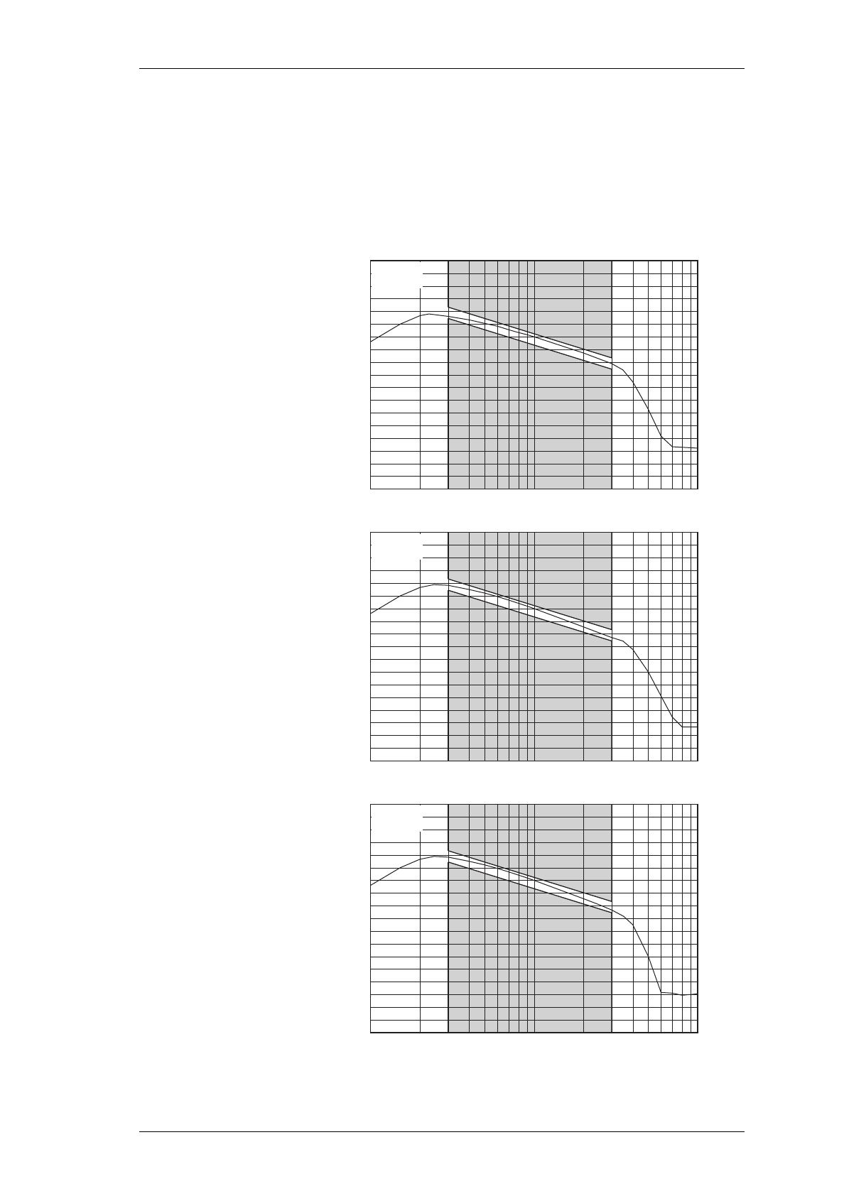
M830-00
T835 Functional Testing
B4.5
Copyright TEL 30/04/98
4.6 De-emphasised Audio Frequency Response
Set RV210 (front panel line level) to provide 0dBm output at 1kHz modulating fre-
quency.
Sweep the modulating frequency, checking that the line audio response closely
follows that shown in Figure 4.1 - the limits should not be exceeded.
Figure 4.1 T835 De-emphasised Audio Frequency Response
Wide Bandwidth
Narrow Bandwidth
+25
+20
Audio Level (dB ref. to O/P @ 1kHz)
+15
+10
+5
+0
-5
-10
-15
-20
-25
-30
-35
-40
-45
-50
-55
100 200 300 500 1k 2k 3k 5k 10k
Frequency (Hz)
25°C 13.8V
Ref. audio power:
+0.0dBm @ 1kHz
+25
+20
Audio Level (dB ref. to O/P @ 1kHz)
+15
+10
+5
+0
-5
-10
-15
-20
-25
-30
-35
-40
-45
-50
-55
100 200 300 500 1k 2k 3k 5k 10k
Frequency (Hz)
25°C 13.8V
Ref. audio power:
-2.2dBm @ 1kHz
Mid Bandwidth +25
+20
Audio Level (dB ref. to O/P @ 1kHz)
+15
+10
+5
+0
-5
-10
-15
-20
-25
-30
-35
-40
-45
-50
-55
100 200 300 500 1k 2k 3k 5k 10k
Frequency (Hz)
25°C 13.8V
Ref. audio power:
-2.5dBm @ 1kHz

B4.6
T835 Functional Testing
M830-00
23/07/99 Copyright TEL
4.7 Noise Mute (If Linked In)
Rotate RV230 (front panel gating sensitivity) fully anticlockwise.
Apply an on-channel signal from the RF generator at a level of -110dBm with
±3kHz deviation (±2.4kHz) [±1.5kHz] at 1kHz.
Increase the RF level in 1dB steps, checking that the mute opens for an RF input
level of approximately -105dBm.
Turn the RF off and check that the mute closes.
Rotate RV230 clockwise and check that the mute opens.
Reset RV230 to give the required opening sinad.
Note:
False opening of the mute can occur if the RF generator’s attenuator is noisy
when the level is being changed.
4.8 RSSI
Apply an on-channel signal from the RF generator at a level of -100dBm with
±3kHz deviation (±2.4kHz) [±1.5kHz] at 1kHz.
Using a high impedance DMM, check that the RSSI output voltage on pin 5 of
D-range 1 (PL100) is 4.5V (nominal).
Vary the RF level in 5dB steps and check that the RSSI output voltage changes at a
rate of approximately 15dB/V over the range of -115dBm to -70dBm (refer to Fig-
ure 4.2 for RSSI voltage vs signal strength).
Figure 4.2 T835 RSSI Voltage vs Signal Strength
RF Level (dBm)
-130 -120 -110 -100 -90 -80 -70 -60
1
2
3
4
5
6
7
8
RSSI Voltage

M830-00
T835 Functional Testing
B4.7
Copyright TEL 23/07/99
4.9 Carrier Level Mute (Carrier Mute Linked In)
Apply an on-channel signal from the RF generator at a level of -120dBm with
±3kHz deviation (±2.4kHz) [±1.5kHz] at 1kHz.
Increase the RF level in 2dB steps and check that the mute opens at an RF level
which corresponds with the preset level on RV235 (carrier mute), i.e. between
-115dBm and -70dBm.
Editor’s Note:
The CTCSS adjustment procedures described in Section 4.10 have
been moved to a more appropriate location in Section 3 as part of
the Initial Tuning & Adjustment procedure (refer to Section 3.4.6
and Section 3.12).


M830-00
T835 Fault Finding
B5.1
Copyright TEL 23/07/99
5 T835 Fault Finding
Caution:
This equipment contains CMOS devices which are susceptible to dam-
age from static charges. Refer to Section 1.2 in Part A for more infor-
mation on anti-static procedures when handling these devices.
The following test procedures and fault finding flow charts may be used to help locate a
hardware problem, however they are by no means a complete fault finding procedure.
If you still cannot trace the fault after progressing through them in a logical manner,
contact your nearest Tait Dealer or Customer Service Organisation. If necessary, you can
get additional technical help from Customer Support, Radio Systems Division, Tait Elec-
tronics Ltd, Christchurch, New Zealand (full contact details are on page 2).
Note 1:
In this and following sections deviation settings are given first for wide
bandwidth sets, followed by settings in brackets for mid bandwidth sets ( )
and narrow bandwidth sets [ ].
Note 2:
Unless otherwise specified, the term "PGM800Win" used in this and follow-
ing sections refers to version 2.00 and later of the software.
Refer to Section 6 where the parts lists, grid reference index and diagrams will provide
detailed information on identifying and locating components and test points on the
main PCB. The parts list and diagrams for the VCO PCB are in Part E.
The following topics are covered in this section.
Section Title Page
5.1 Visual Checks 5.3
5.2 Component Checks 5.3
5.3 Front Panel LED Indicator 5.3
5.4
5.4.1
5.4.2
5.4.3
DC Checks
Power Rails
VCO Locking
Mute Operation
5.4
5.4
5.4
5.4
5.5
5.5.1
5.5.2
5.5.3
5.5.3.1
5.5.3.2
5.5.4
5.5.5
RF Checks
VCO Frequency
RF Sensitivity
Oscillator Stability
TCXO
Second IF
Demodulator Output
IF Distortion
5.5
5.5
5.5
5.6
5.6
5.6
5.6
5.7

B5.2
T835 Fault Finding
M830-00
23/07/99 Copyright TEL
5.6 PGM800Win Generated Errors 5.8
5.7
5.7.1
5.7.1.1
5.7.1.2
5.7.1.3
5.7.2
5.7.3
5.7.4
5.7.5
5.7.6
5.7.7
Fault Finding Charts
Microcontroller
Basic Checks
Serial Communication
CTCSS Decode
Regulator
Synthesiser
Noise Mute
Carrier Mute
Receiver
Audio
5.9
5.9
5.9
5.10
5.11
5.12
5.13
5.16
5.17
5.18
5.19
Figure Title Page
5.1
5.2
5.3
RF Test Cable
IF Swept Response
Ceramic Filter Swept Response
5.5
5.7
5.7
Section Title Page
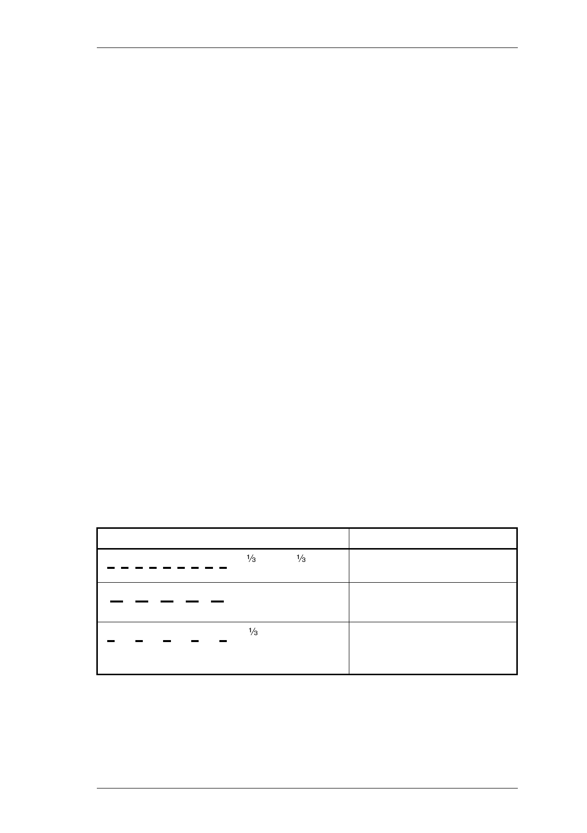
M830-00
T835 Fault Finding
B5.3
Copyright TEL 30/04/98
5.1 Visual Checks
Remove the covers from the T835 and inspect the PCB for damaged or broken compo-
nents, paying particular attention to the surface mounted devices (SMDs).
Check for defective solder joints. If repair or replacement of components is considered
necessary, refer to Section 3 of Part A.
5.2 Component Checks
If you suspect a transistor is faulty, you can assess its performance by measuring the for-
ward and reverse resistance of the junctions. Unless the device is completely desol-
dered, first make sure that the transistor is not shunted by some circuit resistance. Use a
good quality EVM (e.g. Fluke 75) for taking the measurements (or a 20k ohm/V or bet-
ter multimeter, using only the medium or low resistance ranges).
The collector current drawn by multi-junction transistors is a further guide to their per-
formance.
If an IC is suspect, the most reliable check is to measure the DC operating voltages. Due
to the catastrophic nature of most IC failures, the pin voltages will usually be markedly
different from the recommended values in the presence of a fault. The recommended
values can be obtained from either the circuit diagram or the component data catalogue.
5.3 Front Panel LED Indicator
The green "Supply" LED on the receiver front panel will flash according to the condi-
tions described in the following table:
Where two or more conditions occur at the same time, the precedence is in the order
shown above (i.e. receiver linked has the highest priority, followed by VCO error, then
internal error).
Flash Rate Condition
fast ( sec. on/ sec. off
approx.) receiver is linked with
PGM800Win
slow (1 sec. on/1 sec. off
approx.) VCO is out of lock -
refer to Section 5.4.2
unequal ( sec. on/1 sec. off
approx.) microcontroller has detected an
internal communications error -
refer to Section 5.7.1

B5.4
T835 Fault Finding
M830-00
30/04/98 Copyright TEL
5.4 DC Checks
5.4.1 Power Rails
Refer to the test points & options diagrams in Section 6 for test point locations, and to
the regulator fault finding chart (Section 5.7.2) for fault diagnosis.
Check the 9V (TP602) and 13.8V (TP601) power supply test points in the regulator
compartment with a DMM.
Check the 20V regulator output at the test point (TP603) in the regulator compart-
ment.
Check the 5V regulator output at the test point (TP604) in the regulator compart-
ment and on IC350 pin 4.
Check the 5V digital regulator output at the junction of C611A (+) and IC610 pin 2
in the regulator compartment.
5.4.2 VCO Locking
Using a DMM, monitor the VCO control voltage at PL4-1 or the junction of L1 &
R1 on the VCO PCB.
If the synthesiser is locked and the VCO aligned, the voltage at this point should
be between 5 and 13V.
If the VCO is not locked, refer to the synthesiser fault finding charts (Section 5.7.3).
5.4.3 Mute Operation
The front panel "Gate" LED will show the status of the mute circuitry and will turn on
when a signal is received above the threshold level.
Check that PL250 is linked correctly:
noise mute 1-2
carrier mute 2-3.
Check that the mute gate opens as follows:
noise mute - rotate RV230 (front panel gating sensitivity) fully clock-
wise and check that the front panel "Gate" LED turns on;
carrier mute - rotate RV235 (carrier mute) fully clockwise and check that
the front panel "Gate" LED turns on.
If the mute fails to operate correctly, refer to the noise mute fault finding chart (Section
5.7.4) or the carrier mute fault finding chart (Section 5.7.5).

M830-00
T835 Fault Finding
B5.5
Copyright TEL 30/04/98
5.5 RF Checks
5.5.1 VCO Frequency
Check that the VCO is phase locked (refer to Section 5.4.2).
Connect a frequency counter (level +19dBm) to the VCO input to the mixer
(IC410).
Monitor the local oscillator frequency and check that it is 21.4MHz above the
required receive frequency.
Refer to the synthesiser fault finding charts (Section 5.7.3) for further information.
5.5.2 RF Sensitivity
Ensure that the VCO is on the correct frequency and the receiver correctly aligned.
Check that links SL405 to SL440 and link B in the front end are set correctly for the
operating frequency (refer to Section 3.7).
Check that the 12dB sinad sensitivity into the front end is as follows:
-117dBm (de-emphasised response)
-111dBm (flat response).
If the sensitivity is poor, you can trace the fault by measuring the sensitivity into
successive circuit blocks. Prepare a test cable by connecting a 1nF capacitor to the
end of a length of coax cable as shown in Figure 5.1.
Figure 5.1 RF Test Cable
Note:
Before using the test cable, ensure the coax braid is connected to an earth
point on the PCB.
Using the RF test cable, apply a modulated 21.4MHz signal to the test breaks in
the IF section, or an on-channel RF signal to the front end test breaks.
Check that the sensitivity at each test break is within 2dB of the levels shown on
the circuit diagram.
Poor sensitivity indicates a fault in one of the circuit blocks following the test break.
1nF
Coax
To Test Cable
Connect To Earth

B5.6
T835 Fault Finding
M830-00
23/07/99 Copyright TEL
Note:
Poor sensitivity into the mixer can be caused by lack of drive level from the
VCO (the drive level should be >+17dBm).
Refer to the receiver fault finding charts (Section 5.7.6) for further information.
5.5.3 Oscillator Stability
5.5.3.1 TCXO
While maintaining a low level unmodulated RF input to the receiver, loosely cou-
ple into the first IF an additional high level signal at 21.4MHz - you should now
hear a constant low frequency beat note.
Tap the TCXO with a finger and replace it if the beat note permanently changes.
5.5.3.2 Second IF
While maintaining a low level unmodulated RF input to the receiver, loosely cou-
ple into the second IF an additional high level signal at 455kHz - you should now
hear a constant low frequency beat note.
Adjust the frequency of the 455kHz signal for zero beat.
If the second IF is more than 300Hz off frequency, check IC340, X310, C345 and
C347 and replace if necessary.
5.5.4 Demodulator Output
Apply an on-channel RF signal modulated by 1kHz with ±3kHz (±2.4kHz)
[±1.5kHz] deviation at an amplitude of -65dBm.
Connect an oscilloscope probe (DC coupled) to IC350 pin 7 (audio output).
Check that an audio signal of approximately 380mV peak to peak is present.
With the audio response set to flat, optimum tuning of the quad coil (L360) for mini-
mum audio distortion should coincide with maximum audio amplitude and a DC level
of approximately 1.3V.
M830-00
T835 Fault Finding
B5.7
Copyright TEL 23/07/99
5.5.5 IF Distortion
If the audio distortion is still high after careful IF alignment (Section 3.7), sweep the IF to
investigate the bandpass response.
Apply an on-channel RF signal modulated at 10Hz (sine wave) with approxi-
mately ±12kHz (±9kHz) [±6kHz] deviation at an amplitude of -80dBm.
Connect the modulating 10Hz audio signal to the "X" input of an oscilloscope and
observe the 455kHz IF input to IC350 pin 16 via a suitable RF probe on the "Y"
input. Alternatively, use an oscilloscope probe for the "Y" input to monitor the
RSSI output voltage at TP310 (RSSI test point) or pin 5 of D-range 1 (PL100). This
will give a demodulated log response and only the top half of the wave forms
shown in Figure 5.2 and Figure 5.3 will be displayed on the oscilloscope screen.
Note:
The X input should be DC coupled.
Check that the swept response has a rounded top and no sharp non-linearities
(refer to Figure 5.2).
Increase the RF level to -50dBm; the trace will now show the shape of the 455kHz
ceramic filter (&XF340).
Check that the response has no sharp non-linearities.
If sharp non-linearities do occur, replace the filter and sweep again to confirm a
satisfactory solution (refer to Figure 5.3).
Figure 5.2 IF Swept Response Figure 5.3 Ceramic Filter Swept Response

B5.8
T835 Fault Finding
M830-00
30/04/98 Copyright TEL
5.6 PGM800Win Generated Errors
The following errors are those most likely to occur using PGM800Win. Refer to the
PGM800Win software user’s manual for a complete list of error messages.
Channel Switch Set
The programmed default channel was not accepted by the base station because a chan-
nel is selected externally. Try turning the external channel switch off before changing
the default channel in PGM800Win.
Synth Out Of Lock
The synthesiser received incorrect data, or the data was corrupted. Enter a frequency
within the VCO switching range, or tune the VCO.
Internal Error
Data could not be read from the base station due to an internal error. Check for shorts or
open circuits on the SDA, SCK, SYNTH and EPOT lines. The SDA, SCK and SYNTH
are normally high.
Write/Read To An Unlinked Module
The link to the module does not exist. Undefined error.
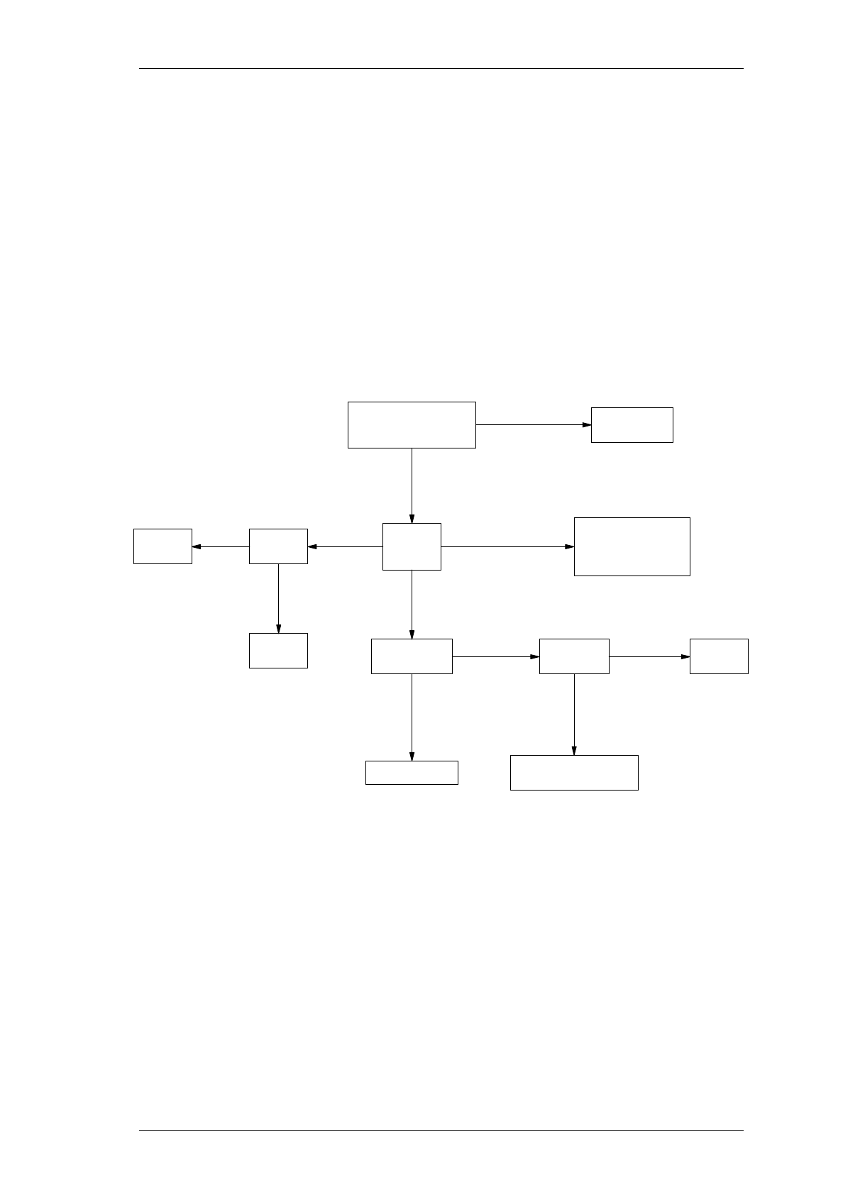
M830-00
T835 Fault Finding
B5.9
Copyright TEL 30/04/98
5.7 Fault Finding Charts
Note:
The standard test point designations used in this section are as follows:
TP601 13.8V
TP602 9V
TP603 20V
TP604 5V
5.7.1 Microcontroller (IC810)
5.7.1.1 Basic Checks
Pulsing Check state
of pin 35.
Y
Is pin 30
pulsing?
High or open circuit
Y
Static high/low
Check state of
pins 36 to 43.
Low/floating
High
Is the 12.8MHz clock
present on IC810 pin 21
(microcontroller)?
N
Replace
IC810.
Check IC740
(synthesiser).
*digital storage oscilloscope
Replace IC810.
Check the
state of
pin 10.
N Pulsing
Low
Replace
IC810.
Use a DSO* to check
operation of IC650
(i.e. active high
pulse at power up).
Replace
IC650.
Correct the fault causing
pin 35 to be low/floating.
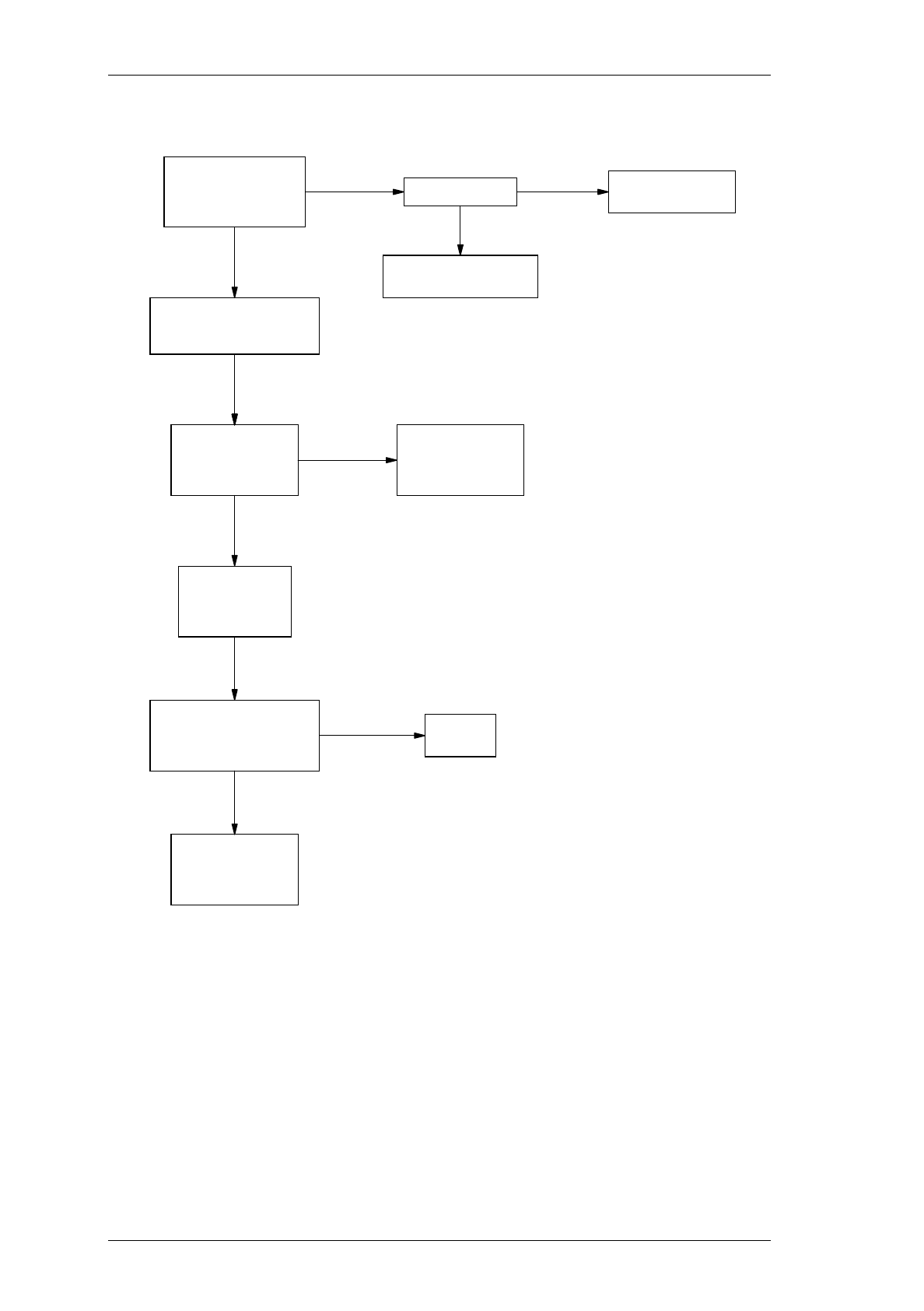
B5.10
T835 Fault Finding
M830-00
30/04/98 Copyright TEL
5.7.1.2 Serial Communication
Check pin state.
Y
Low/floatin
g
N
Noise
on pin
Disconnect the
pro
g
rammin
g
lead.
Is IC810 pin 11 hi
g
h?
(microcontroller)
Y*di
g
ital stora
g
e
oscilloscope
Use PGM800Win
to send a POLL
command to the
radio.
Check the transistor
interface circuitry
and/or replace the
pro
g
rammin
g
lead.
Check the SERIAL-COM
and AUDIO-1/2 links.
Replace
IC810.
Check the transistor
interface circuitry
and/or replace the
pro
g
rammin
g
lead.
Check the transistor
interface circuitry.
Check IC810 pin 13
with a DSO. Is there
a response from IC810 after
a poll command is sent?
N
Y
Connect the pro
g
rammin
g
lead and use PGM800Win
to read the rack/radio.
Check I/O pad P810
with a DSO*.
Does it swin
g
from
0 to 5V?
N
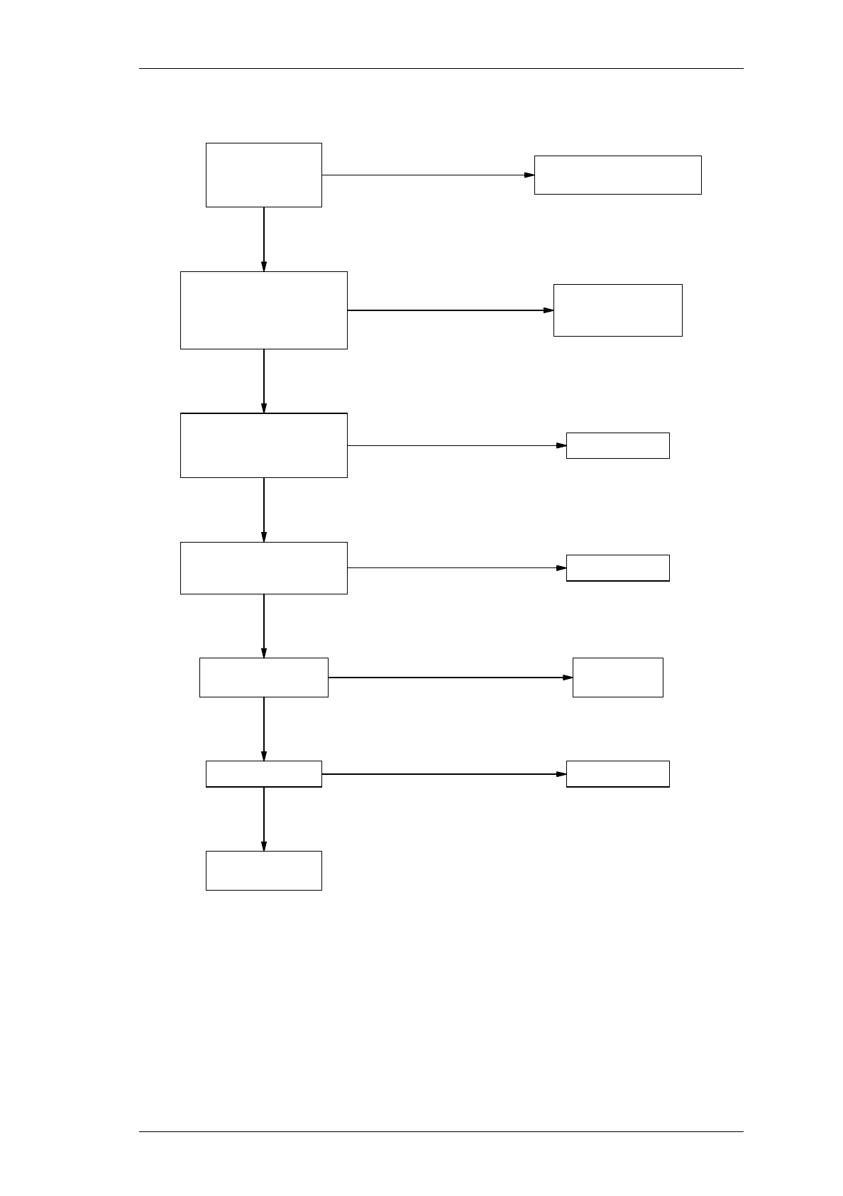
M830-00
T835 Fault Finding
B5.11
Copyright TEL 30/04/98
5.7.1.3 CTCSS Decode
Y
No square wave or
uneven mark/space ratio
Use PGM800Win to
select a channel
with a CTCSS tone
pro
g
rammed.
Check serial communications.
(See separate flow chart).
Cannot select a channel
Check IC810 pins 24 & 26
(microcontroller).
Are there 5V square waves at
the CTCSS frequency?
Y
Check IC850 pins 1 & 14.
Are there 9V square waves at
the CTCSS frequency? Replace IC850.
Y
Is IC850 pin 7 low and
Q845 collector hi
g
h? Replace IC850
or Q845.
N
Y
Is IC810 pin 31 low? Replace IC810.
N
Y
Check the receiver
mute circuit.
Set test equipment to correct
channel/CTCSS tone.
Check IC830 pin 7.
Is there a square wave at
the CTCSS input frequency?
Replace IC810.
No square waves or
uneven mark/space ratio
No square waves or
uneven mark/space ratio
Check the input filter
is operatin
g
correctly
(IC830 pin 8).
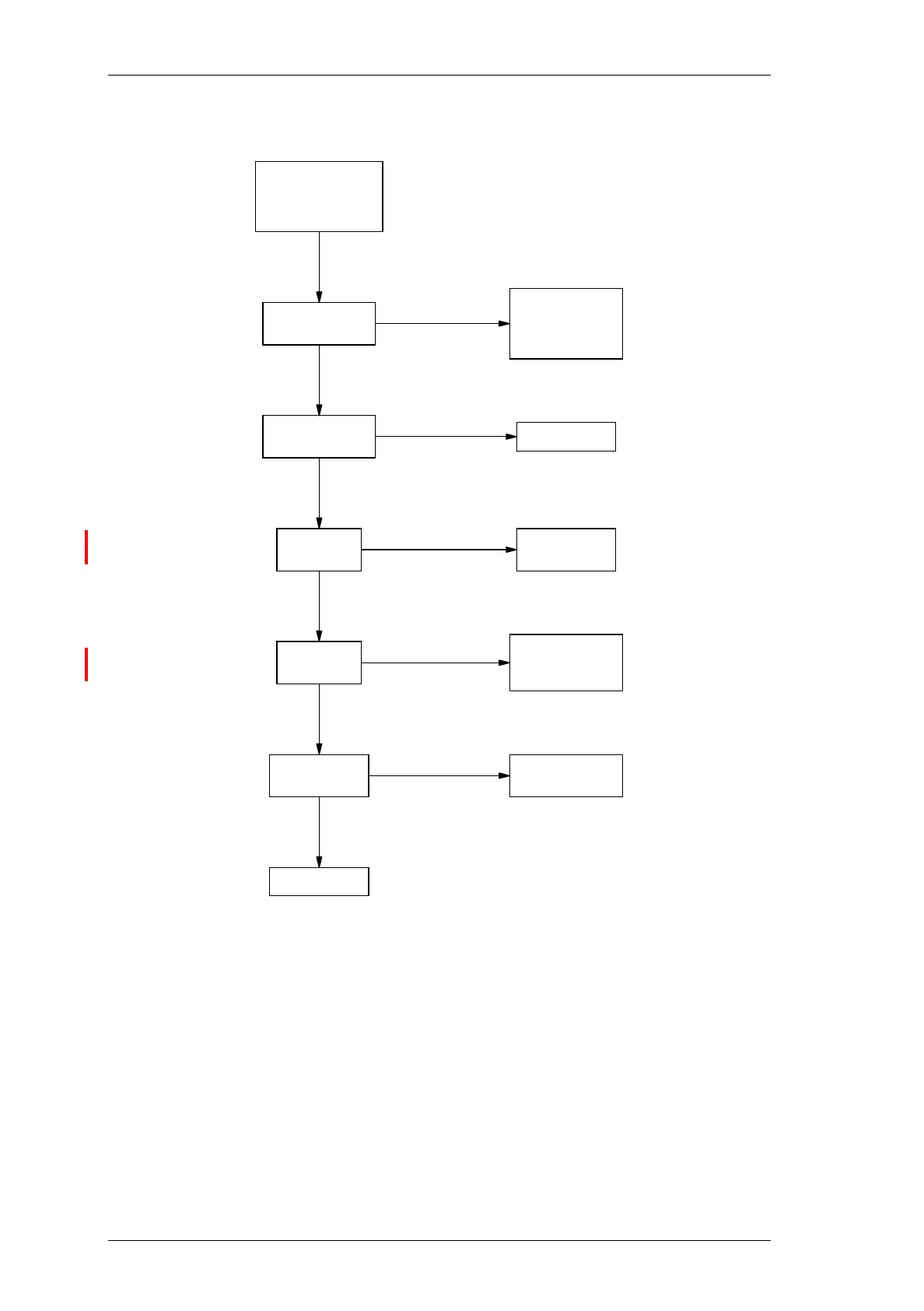
B5.12
T835 Fault Finding
M830-00
23/07/99 Copyright TEL
5.7.2 Regulator
Check for
overheatin
g
components &
short circuits.
13.8V present on
IC630 pin 3?
5.3V present on
IC630 pin 1?
Check Q620,
Q630 & IC640.
Check Q660 is
switchin
g
at
approx. 180kHz.
5V present on
IC610 pin 2?
Replace IC630.
Check R615.
Replace IC610.
Check continuity
from D-ran
g
e
connector pin 9.
(D-ran
g
e 1)
N
Y
N
Y
N
Y
N
Y
N
Re
g
ulators OK.
Y
20V present
on TP603?
9.0V present
on TP602?
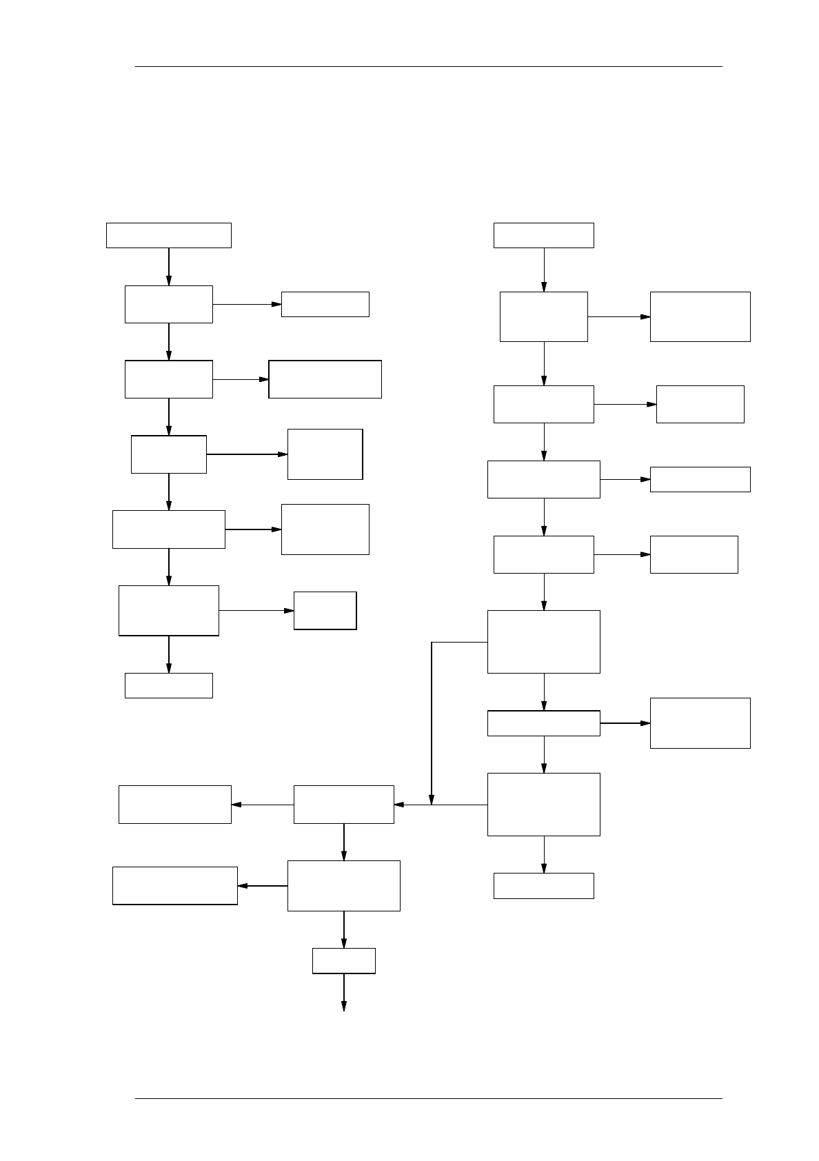
M830-00
T835 Fault Finding
B5.13
Copyright TEL 30/04/98
5.7.3 Synthesiser
Refer to the synthesiser circuit diagram (sheet 7) in Section 6 and the VCO circuit dia-
gram in Part E.
N
A B
Check biasin
g
resistors, Q4 & Q5.
Check 9V re
g
.
N
Y
N
8.3V present
at VCO?
DC V present
at Q4 & Q5?
9V present at
VCO Q4/Q5?
Check Q4 C
multiplier
(synth).
No VCO RF output.
Y
DC V present at
VCO, Q1, Q2 & Q3?
Check biasin
g
resistors, Q1,
Q2 & Q3.
Y
N
Capacitors OK?
Check for cracks,
shorts, etc.
N
Y
Replace VCO.
Replace
if faulty.
Y
N
N
N
N
Y
Y
Check biasin
g
resistors & Q1.
DC V present
on Q795 emitter?
Check 9V supply.
9V present on
Q795 divider buffer?
20V inverter
supply faulty.
20V present
on IC750 pin 8?
Check 5V re
g
. &
supply resistor
to each IC.
VCO out of lock.
Y
Y
Y
Continued on the next pa
g
e
Y
Does VCO trimmer
adjust for stable
control line
between 5 & 13V?
VCO freq. correct?
Does VCO trimmer
adjust for required
frequency ran
g
e
between 5 & 13V?
Synthesiser OK.
VCO trimmer
freq. ran
g
e OK?
Check VCO tunin
g
caps & trimmer.
Is 8MHz VCO ran
g
e
achieved between
5 & 13V?
VCO OK.
N
N
NN
N
Y
Y
Recheck
pro
g
rammin
g
via PGM800Win.
Y
+5V present at
IC700, IC710
& IC740?
Check #C5, #C3, #C4,
CV1 & D1-D4 in VCO.
B5.14
T835 Fault Finding
M830-00
30/04/98 Copyright TEL
Programming and
serial bus OK?
Is reference
clock present
at IC740 pin 20
(12.8MHz >1.5Vpp)?
Check programming.
Check serial bus
when programming
i.e. clock/data/enable
activity (IC740 pins
18, 19 & 17). NN
Check loop filter components
R775, C774, C776, R510,
C505, IC750. Is the supply
to IC750 +20V +4, -2V?
Check regulator circuitry.
Check C772, R774, R772,
C770, R763 & Q790.
Check Q760, Q780,
R766 & C765.
Check charge pump components
(Q775 & Q780) and Q790.
Check R762 & C762.
Check the signal path from
the VCO to synthesiser.
Measure the frequency from
the VCO at IC740 pin 11 using
a frequency counter.
Is the level >-10dBm?
Does the frequency adjust
as the VCO trimmer is
adjusted (out of lock)?
Check VCO.
Y
Y
Y
Signal
Y
Y
Y
No signal
Replace synthesiser
(IC740).
Y
N Y
Y
N
N
N
N
Check phase detector output
pins (IC740 pins 3 & 4).
Are there very narrow pulses
(~50ns) at the reference frequency?
(i.e. 5kHz : 200µs period
6.25kHz : 160µs period)
*See Note below.
Is the charge pump bias
voltage at the base of
Q760 & Q780 between
3.5 and 5V? (5V when locked)
N
Is the voltage on C762,
R760, and R758 9V ±0.2V?
Is the loop filter reference
voltage at C772 (+) 6.5V ±0.2V?
N
Check divider buffer
circuit (Q795) and bias
voltages on Q795 emitter
(1.3V ±0.2V).
*Note:
When locked, both of these
are very narrow (~50ns).
If unlocked, one will be
very narrow (~50ns),
and the other wide (>15µs).
Check microcontroller
section (IC810). Check TCXO (IC700)
and buffers (IC710).
Replace synthesiser
(IC740).
Continued from previous page
B
Is the charge pump voltage
on Q790 gate between
3 and 8.5V? (6.5V ±0.2V locked)
M830-00
T835 Fault Finding
B5.15
Copyright TEL 30/04/98
Y
N
Y
Y
Y
Y
N
Y
Y
Y
C
Noisy synth; poor
selectivity &/or
poor residual FM.
VCO phase locked?
5-13V present on
control line?
Correct DC V
present on Q1 VCO?
Change trimmer;
still noisy?
Change Q1;
still noisy?
Change TCXO;
still noisy?
Change varactors;
still noisy?
Replace VCO
assembly.
Synthesiser OK.
N
N
N
N
Check inductors,
biasing resistors
& Q1.
Replace if faulty.
Go to B.
Loop filter &
components around
op. amp. (IC750) OK?
N
B5.16
T835 Fault Finding
M830-00
23/07/99 Copyright TEL
5.7.4 Noise Mute
Apply on channel signal
@ -117dBm* to receiver.
Refer to audio
fault finding chart.
Ensure PL250 is set
for noise mute operation.
Audio on
IC350 pin 7?
Noise on
IC390 pin 7?
Amplified noise
on C395? Check Q340
& Q350.
Check D310 is
rectifying noise.
Vary RF level &
observe voltage
on pad 236.
Pad 236 voltage
varies 0-1.8V?
Check 9V rail &
resistors R264,
R265 & R284.
Replace IC270.
Check/replace
IC270 & D240.
Replace Q250.
NY
N
Y
N
Y
Y
N
Y
Y
Y
Y
N
Refer to
receiver fault
finding chart.
Check components
around active filter.
Mutable audio
on outputs?
Y
Voltage varies
0-2.5V?
N
OK
Does "Gate" LED
toggle on/off?
N
Check Q230, Q245 &
Q290 for operation.
Y
Adjust RV230
(gating sensitivity)
& observe voltage
on IC270 pin 3.
Set RF signal level to
-117dBm. Rotate
RV230 c/w & cc/w.
Monitor voltage on
IC270 pin 1. Switching
0-8V as RV230 rotated?
Monitor voltage on
IC270 pin 7. Switching
0-8V as RV230 rotated?
Monitor voltage on
pad 234. Switching
0-8V as RV230 rotated?
N
N
N
Does "Gate"
LED toggle? Check/replace
Q255 & D250.
Y
YN
Check RV330
adjustment
(noise mute gain).
Approx. 0.6V DC rect-
ified noise on pad 236?
N
Switch SW201 (monitor
mute) to ensure
mute is enabled.
Rotate RV230
(gating sensitivity)
c/w & cc/w & view
"Gate" LED.
Note:
c/w = clockwise
cc/w = counterclockwise
or anticlockwise
*Modulated by 1kHz signal with
±3kHz (±2.4kHz) [±1.5kHz] deviation
M830-00
T835 Fault Finding
B5.17
Copyright TEL 23/07/99
5.7.5 Carrier Mute
Approx. 5V on
RSSI pad 238?
Approx. 5V on
IC280 pin 1?
Check IC390 and
adjoining components.
Check/replace IC280
& adjoining components.
Check Q230, Q245 &
Q290 for operation. Adjust RV235 &
observe voltage
on IC280 pin 6.
Switch SW201
(monitor mute) to ensure
mute is enabled.
Y
N
N
N
Y
Y
Does "Gate" LED
toggle on/off?
Check for short circuits
and/or replace IC350.
Refer to
receiver fault
finding chart.
N
N
Y
Y
Voltage varies
0-6V?
Check 9V rail &
resistors R275,
R277 & RV235.
Y
N
Set RF signal level
to -95dBm. Rotate
RV235 c/w & cc/w.
Monitor voltage on
IC280 pin 7. Switching
0-8V as RV235 rotated? Replace IC280.
N
Y
Monitor voltage on
IC270 pin 7. Switching
0-8V as RV235 rotated?
Check/replace
IC270 & D240.
N
Y
Monitor voltage on
pad 234. Switching
0-8V as RV235 rotated? Replace Q250.
N
Y
Does "Gate"
LED toggle? Check/replace
Q255 & D250.
YN
Mutable audio
on outputs?
OK
N
Y
Refer to audio
fault finding chart.
Note:
c/w = clockwise
cc/w = counterclockwise
or anticlockwise
Rotate RV235
(carrier mute) c/w & cc/w
& view "Gate" LED.
Ensure PL250 is set
for carrier mute operation,
and the RSSI PCB is fitted.
Apply on channel signal
@ -95dBm* to receiver.
Audio on
IC350 pin 7?
Approx. 3.3V on
IC350 pin 5?
*Modulated by 1kHz signal with
±3kHz (±2.4kHz) [±1.5kHz] deviation.
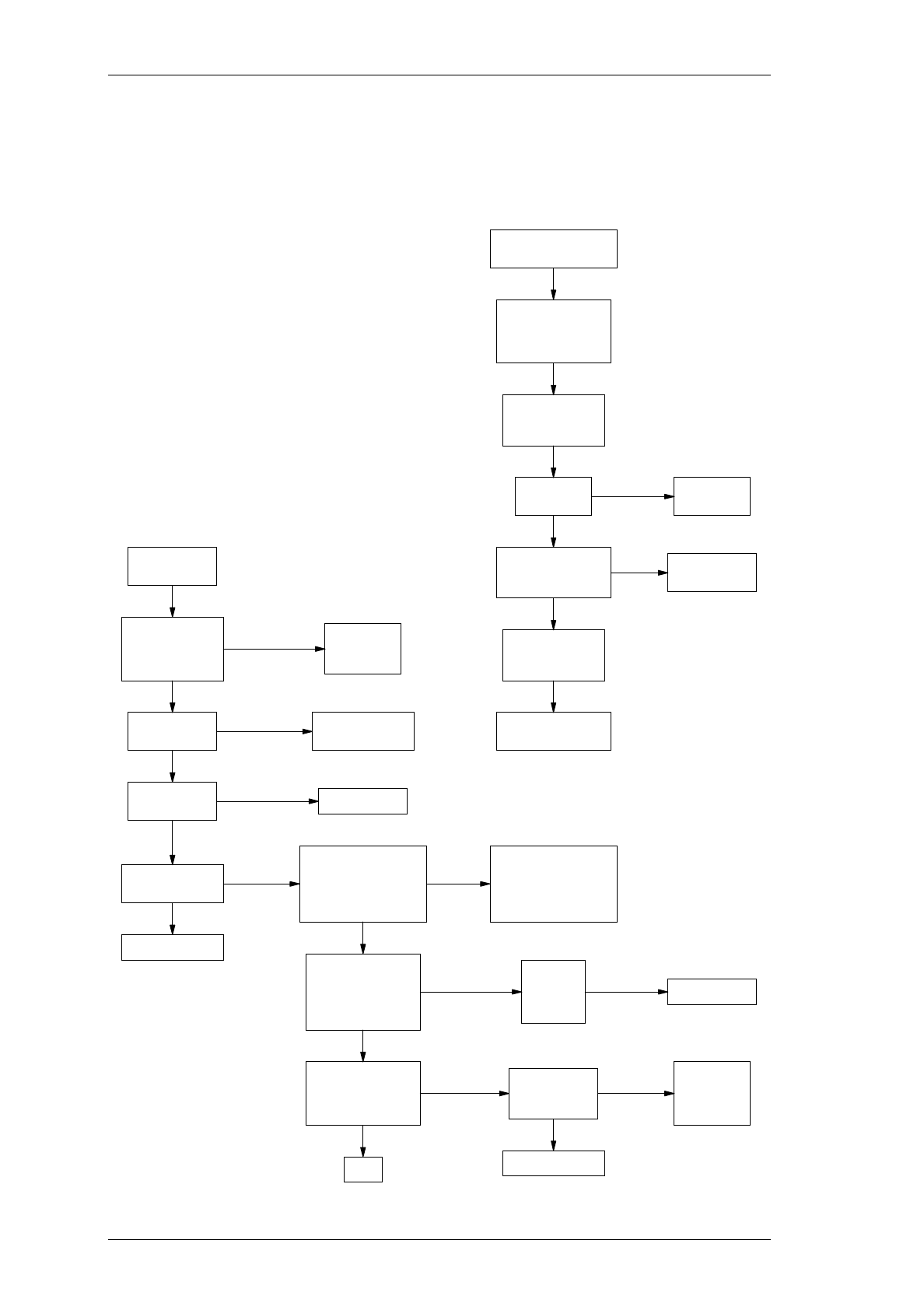
B5.18
T835 Fault Finding
M830-00
30/04/98 Copyright TEL
5.7.6 Receiver
Refer to the receiver IF and front end circuit diagrams (sheets 3 & 4) in Section 6.
High audio
distortion.
B
Note: T.B. = Test Break
(refer circuit diagrams)
Quad coil L360
tuned for min.
distortion (flat
audio response)?
Adjust L360.
Retune all
IF coils.
Check VCO
frequency OK? Readjust TCXO
frequency.
Check IF
alignment OK? Adjust IF coils.
Check distortion
IC350 pin 7 OK?
Fault find audio.
Check distortion
IC350 pin 7,
injecting 21.4MHz
@ -47dBm into T.B.
at &XF330 input. OK?
Fault in IC350,
&XF340, IC340,
&XF330 or
surrounding circuitry.
Check/replace.
Inject 21.4MHz
after mixer IF
output T.B.
Measure distortion.
OK?
Inject on-channel
RF into mixer T.B.
Measure distortion.
OK?
OK
Check
sensitivity
into each
IF stage.
Repair stage.
Replace TCXO.
Refer to
synthesiser
fault finding
charts.
Check TCXO
stability OK?
(see 5.5.3)
N
Y
N
Y
N
Y
N
Y
N
Y
N
Y
NY
Y
Y
Ensure VCO, RF
front end & IF
correctly aligned.
High audio
distortion?
Check/repair faulty
stage or component.
Check DC
conditions OK?
(see cct diagrams)
Check sensitivity
into each stage
(see 5.5.2)
See Chart B
(below).
Replace
faulty device.
Y
N
N
Y
Ensure links SL405
to SL440 & link B
are set correctly.
(see Section 3.7)
Poor sensitivity:
worse than -117dBm.
A
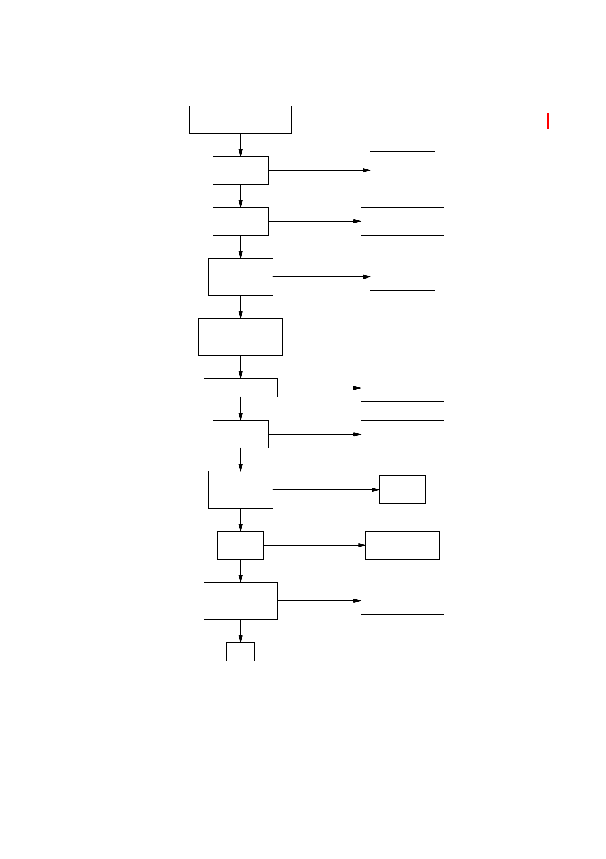
M830-00
T835 Fault Finding
B5.19
Copyright TEL 23/07/99
5.7.7 Audio
Audio on
IC350 pin 7?
Audio on
IC210 pin 1? Check components
around IC210.
Apply on channel si
g
nal
@ -117dBm* to receiver.
Refer to
receiver fault
findin
g
chart.
Ensure RV230
(
g
atin
g
sensitivity)
fully clockwise.
"Gate" LED on? Refer to mute
fault findin
g
charts.
Y
N
N
Y
N
Y
N
Y
Audio on
speaker?
Audio on
C238/C259?
Audio on
IC240 pin 2 &
IC260 pin 2?
Replace C249 &
check continuity.
Audio on line
monitor (pad 284)
& line output?
Refer to mute
fault findin
g
charts.
OK
Check/replace
output components.
N
Y
N
Y
N
Y
N
Y
Audio at
top of RV205
& RV210?
Check C233 &
PL240 link.
Replace
faulty IC.
*Modulated by 1kHz si
g
nal with
±3kHz (±2.4kHz) [±1.5kHz] deviation.

M830-00
T835 PCB Information
B6.1.1
Copyright TEL 23/07/99
6 T835 PCB Information
Caution:
This equipment contains CMOS devices which are susceptible to damage from
static charges. Refer to Section 1.2 in Part A for more information on anti-static
procedures when handling these devices.
This section provides the following information on the T835 receiver:
•parts lists
• grid reference index
• mechanical assembly drawing
•PCB layouts
• test points & options connections drawings
• circuit diagrams.
Section Title IPN Page
6.1 Introduction 6.1.3
6.2 T835 Receiver PCB 220-01394-02 6.2.1

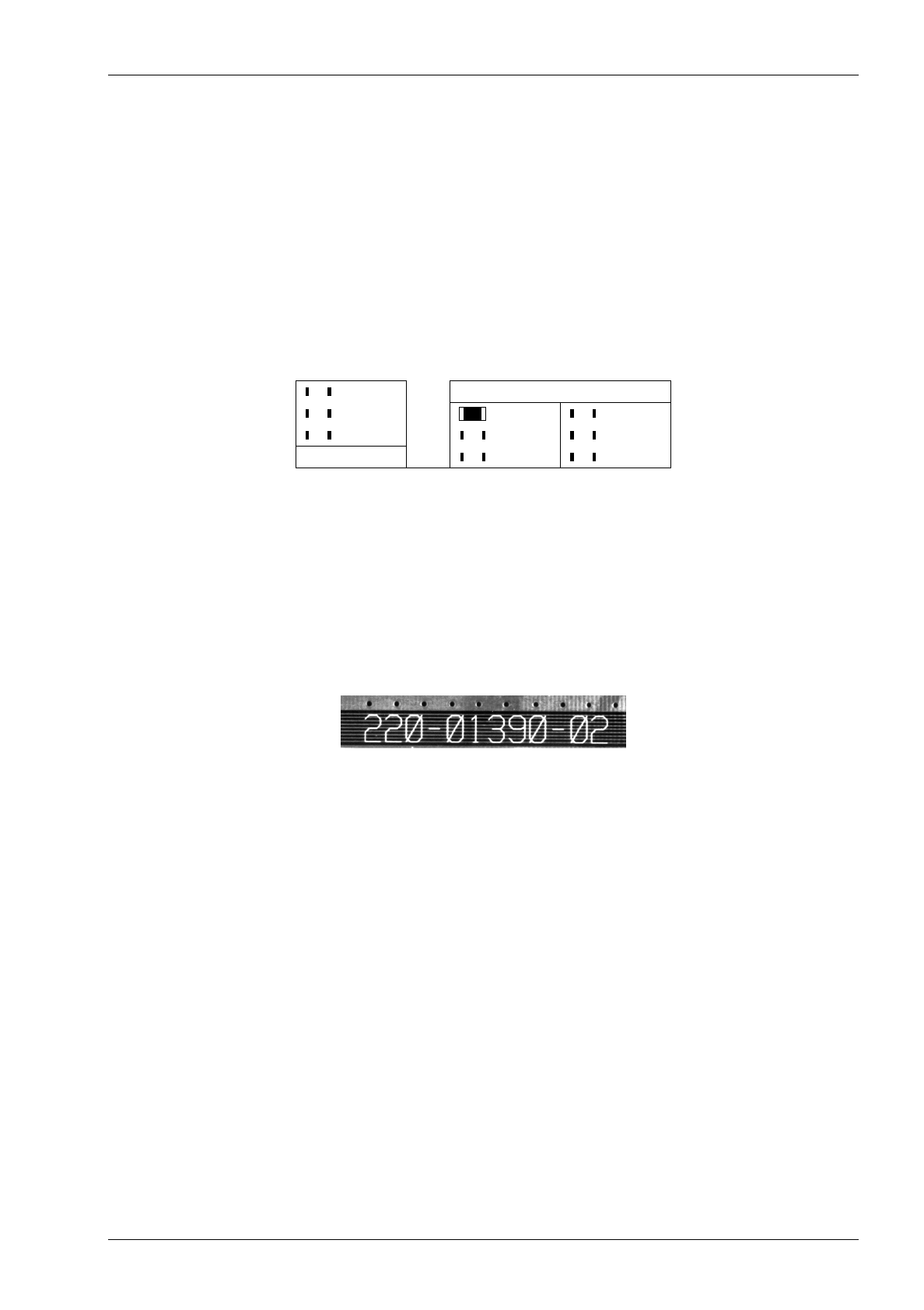
M830-00
T835 PCB Information
B6.1.3
Copyright TEL 30/04/98
6.1 Introduction
Product Type Identification
You can identify the receiver type by checking the product code printed on a label on the rear of the
chassis (product codes are explained in Section 1.3 in this Part of the manual, and Figure 1.1 in Part
A shows typical labels). You can further verify the receiver type by checking the placement of an
SMD resistor in the table that is screen printed onto the top side of the PCB, similar to the example
drawn below (this table also appears in the resist layer on the bottom side of the PCB). In this exam-
ple, the resistor indicates that the product was built as a T835-10-XXXX.
Note:
The only function of this resistor is to indicate the product type. It has no effect on the
circuitry or operation of the receiver.
PCB Identification
All PCBs are identified by a unique 10 digit “internal part number” (IPN), e.g. 220-12345-00, which
is screen printed onto the PCB (usually on the top side), as shown in the example below:
The last 2 digits of this number define the issue status, which starts at 00 and increments through 01,
02, 03, etc. as the PCB is updated. Some issue PCBs never reach full production status and are there-
fore not included in this manual. A letter following the 10 digit IPN has no relevance in identifying
the PCB for service purposes.
Note:
It is important that you identify which issue PCB you are working on so that you can
refer to the appropriate set of PCB information.
835- PRODUCT TYPE
835- 835-10 835-20
835- 835-13 835-23
PRODUCT TYPE 835-15 835-25
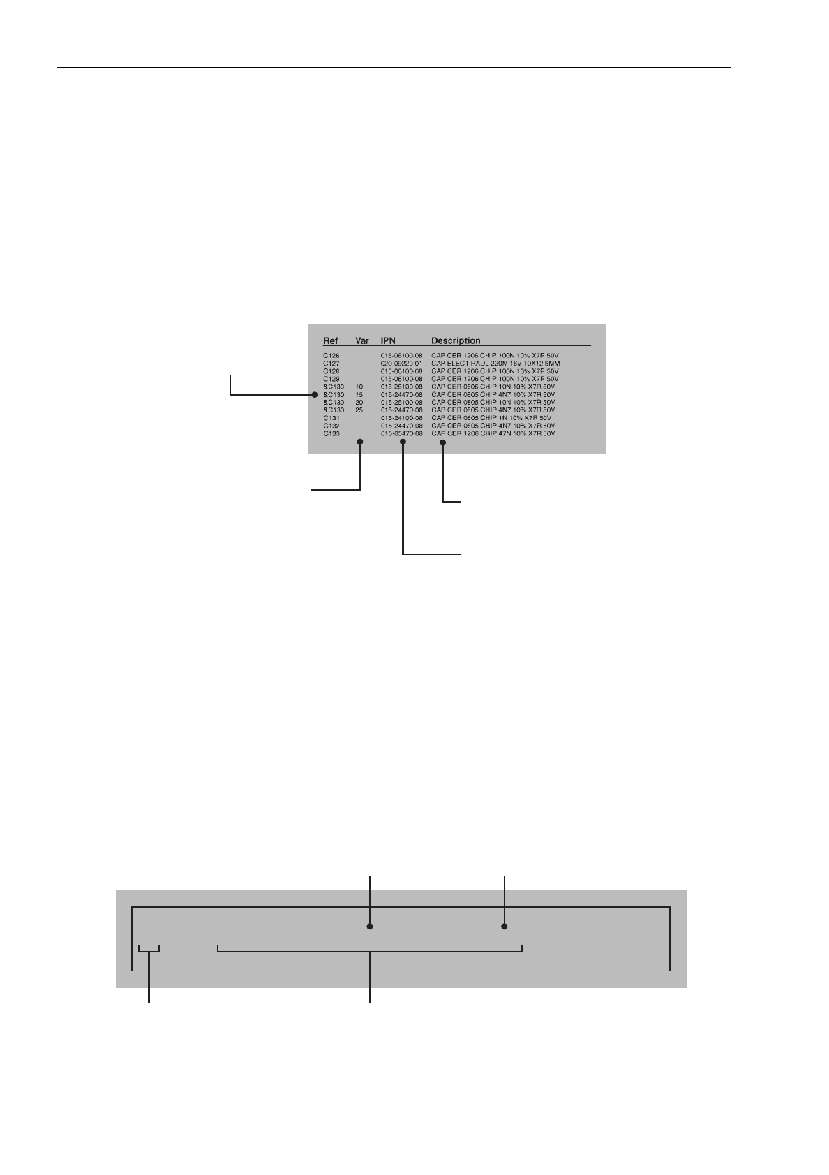
B6.1.4
T835 PCB Information
M830-00
30/04/98 Copyright TEL
Parts Lists
The 10 digit numbers (000-00000-00) in this Parts List are “internal part numbers” (IPNs). We can
process your spare parts orders more efficiently and accurately if you quote the IPN and provide a
brief description of the part.
The components listed in this parts list are divided into two main types: those with a circuit refer-
ence (e.g. C2, D1, R121, etc.) and those without (miscellaneous and mechanical).
Those with a circuit reference are grouped in alphabetical order and then in numerical order within
each group. Each component entry comprises three or four columns, as shown below:
The mechanical and miscellaneous section lists the variant and common parts in IPN order.
Parts List Amendments
At the front of the parts list is the Parts List Amendments box (an example of which is shown
below). This box contains a list of component changes which took place after the parts list and dia-
grams in this section were compiled. These changes (e.g. value changes, added/deleted compo-
nents, etc.) are listed by circuit reference in alphanumeric order and supersede the information
given in the parts list or diagrams. Components without circuit references are listed in IPN order.
The number in brackets at the end of each entry refers to the Tait internal Change Order document.
circuit reference -
lists components
in alphanumeric
order
variant column -
indicates that this is
a variant component
which is fitted only to
the product type listed
Internal Part Number -
order the component
b
y
this number
description -
gives a brief description
of the component
Parts List Amendments
R306 Changed from 180Ωto 560Ω(036-13560-00) to increase sensitivity (71003).
circuit reference
or IPN description
of change
IPN of new
component Change Order
number
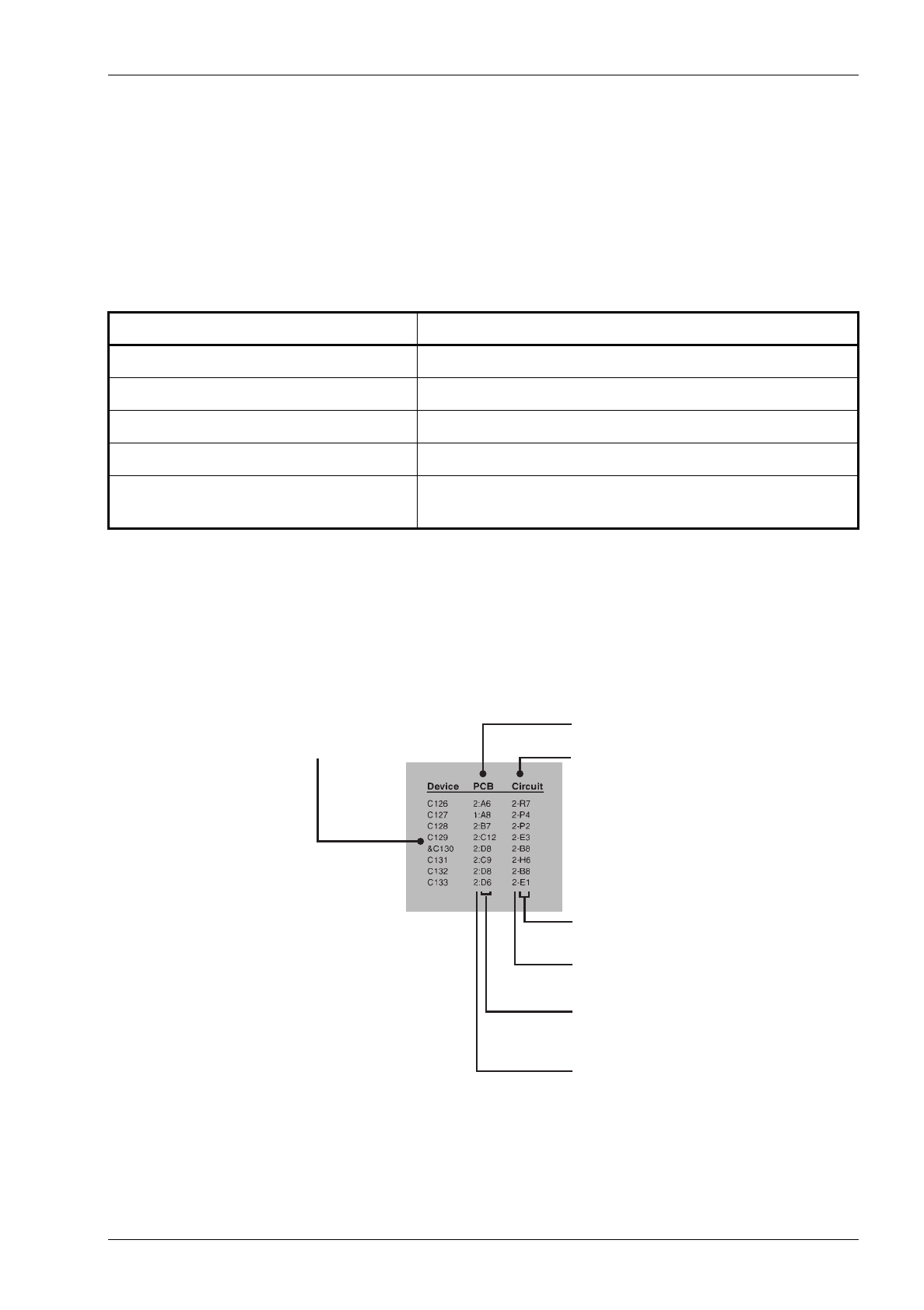
M830-00
T835 PCB Information
B6.1.5
Copyright TEL 30/04/98
Variant Components
A variant component is one that has the same circuit reference but different value or specification in
different product types. Where two products share the same PCB, the term “variant” is also used to
describe components unplaced in one product. Variant components have a character prefix, such as
“&”, “=” or “#”, before the circuit reference (e.g. &R100).
The table below explains the variant prefixes used in T800 Series II products:
Grid Reference Index
This section contains a component grid reference index to help you find components and labelled
pads on the PCB layouts and circuit diagrams. This index lists the components and pads in alpha-
numeric order, along with the appropriate alphanumeric grid references, as shown below:
If the variant prefix is. . . the component will. . .
& change according to channel spacing
= change according to frequency stability
# change according to frequency range
% be placed or unplaced for special applications
*be unplaced in one product
(where two products share the same PCB)
circuit diagram
reference
PCB layout
reference
components listed
in alphanumeric order
layer number -
1 = top side layer
2 = bottom side layer
component location
on the layer
sheet number
component location
on the sheet
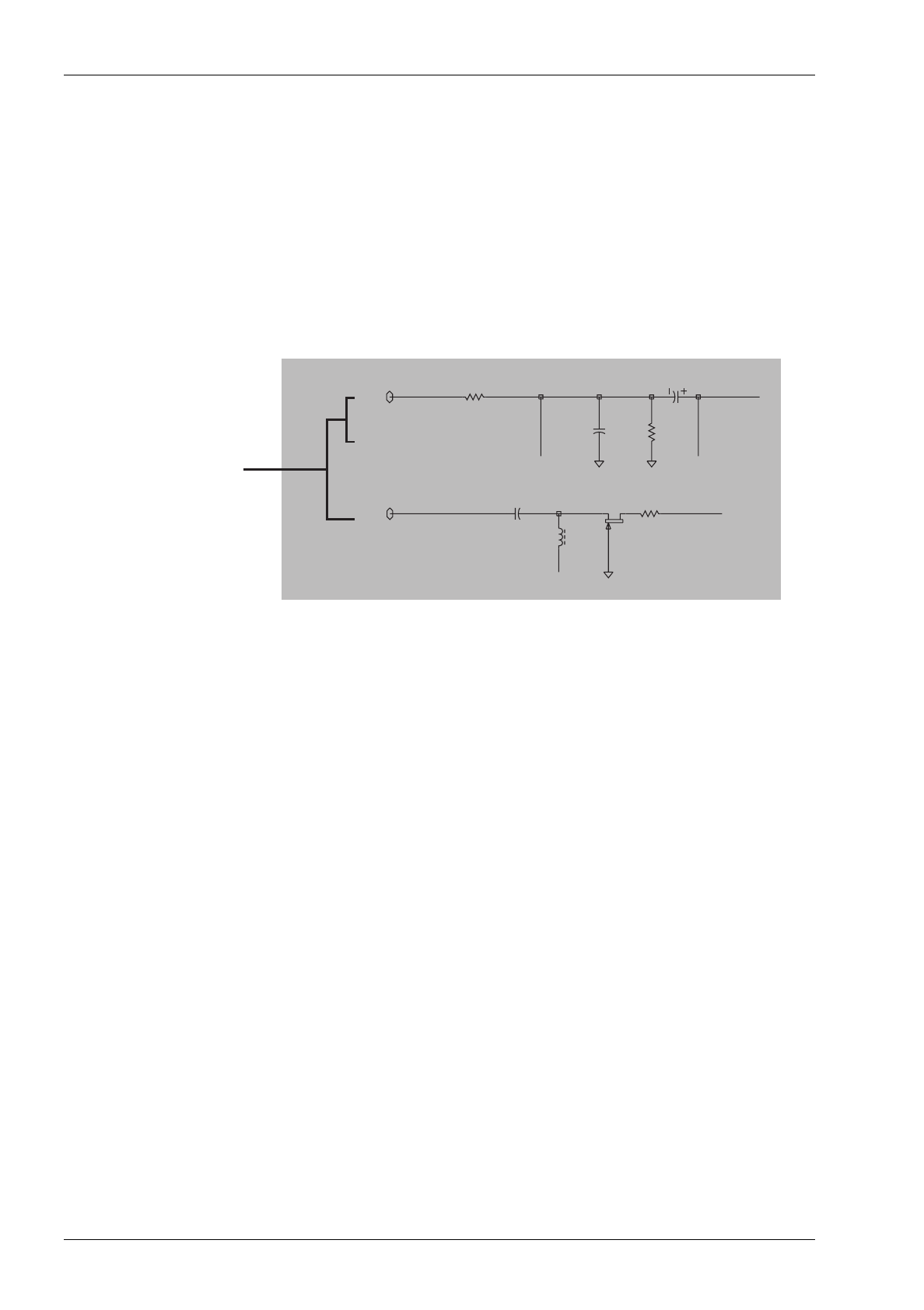
B6.1.6
T835 PCB Information
M830-00
30/04/98 Copyright TEL
Using CAD Circuit Diagrams
Reading a CAD circuit diagram is similar to reading a road map, in that both have an alphanumeric
border. The circuit diagrams in this manual use letters to represent the horizontal axis, and num-
bers for the vertical axis. These circuit diagram “grid references” are useful in following a circuit
that is spread over two or more sheets.
When a line representing part of the circuitry is discontinued, a reference will be given at the end of
the line to indicate where the rest of the circuitry is located, as shown below. The first digit refers to
the sheet number and the last two characters refer to the location on that sheet of the continuation of
the circuit (e.g. 1R3).
C301
4N7
R303
12
D
S
G
L310
33U
IF-SIG
4R4
C369
100P
C371
10U
R339
100K
%R338
100
DISCRIMINATOR
1R3
2R9
2R9
8A2
t
hese grid references
s
how where the circuit
is continued

M830-00
T835 PCB Information
B6.2.1
Copyright TEL 30/04/98
6.2 T835 Receiver PCB
This section contains the following information.
IPN Section Page
220-011394-02 Parts List
Mechanical & Miscellaneous Parts
Mechanical Assembly
Grid Reference Index
PCB Layout - Top Side
PCB Layout - Bottom Side
Test Points & Options Connections - Top Side
Test Points & Options Connections - Bottom Side
Receiver Overview Diagram
Audio Processor Circuit Diagram
IF Section Circuit Diagram
Front End Circuit Diagram
VCO Section Circuit Diagram
Regulators Circuit Diagram
Synthesiser Circuit Diagram
Microcontroller Circuit Diagram
Harmonic Filter Circuit Diagram
6.2.3
6.2.8
6.2.9
6.2.11
6.2.15
6.2.16
6.2.17
6.2.18
6.2.19
6.2.20
6.2.21
6.2.22
6.2.23
6.2.24
6.2.25
6.2.26
6.2.27


IPN 220-01394-02
M830-00
T835 PCB Information
B6.2.3
Copyright TEL 23/07/99
T835 Parts List (IPN 220-01394-02)
How To Use This Parts List
The components listed in this parts list are divided into two main types: those with a circuit reference (e.g. C2, D1, R121, etc.) and
those without (miscellaneous and mechanical).
Those with a circuit reference are grouped in alphabetical order and then in numerical order within each group. Each component
entry comprises three or four columns: the circuit reference, variant (if applicable), IPN and description. A number in the variant col-
umn indicates that this is a variant component which is fitted only to the product type listed. Static sensitive devices are indicated by
an (S) at the start of the description column.
The miscellaneous and mechanical section lists the variant and common parts in IPN order. Where possible, a number in the legend
column indicates their position in the mechanical assembly drawing.
The Parts List Amendments box below lists component changes that took place after the parts list and diagrams in this section were
compiled. These changes (e.g. value changes, added/deleted components, etc.) are listed by circuit reference in alphanumeric order
and supersede the information given in the parts list or diagrams. Components without circuit references are listed in IPN order.
Parts List Amendments
C309 Changed from 33p to 18p (IPN 015-22180-01).
C311 Changed from 39p to 47p (IPN 015-22470-01).
C406, C420
C448, C464
148-174MHz (-20, -23 & -25): changed from 15p (IPN 015-22150-01) to 18p (IPN 015-22180-01) to improve the
front end tuning (710386).
C774 Changed from 330n polyester to 330n polyphenylene-sulphide (IPN 022-06330-05) to improve ultimate signal-to-
noise performance by reducing PLL phase noise (710352).
D111 Changed from MR750 (IPN 001-00011-60) to MR2520L (IPN 001-00012-90) to provide overvoltage transient sup-
pression (750087/88/89/90/91/92).
IC710 Changed from 74HCU04 to 74HC04 (IPN 002-74900-04) to improve ultimate signal-to-noise performance by
reducing PLL phase noise (710352).
Q310 Changed from BF477A (IPN 000-50020-18) to BF247A (IPN 000-00020-18) as BF477A unavailable (710896).
R256 Changed from 4k7 to 2k7 (IPN 036-14270-00).
R419 Changed from 470Ω to 560Ω (IPN 036-13560-00).
R425 Changed from 180Ω to 560Ω (IPN 036-13560-00).
R510 Changed from 680Ω to 2k2 (IPN 036-14220-00).
R775 Changed from 5k6 to 6k8 (IPN 036-14680-00).
RV320 Changed to IPN 042-05470-07 (47k preset) because IPN 042-05470-06 no longer available (710793/96/97/98).
303-11169-03 T800 chassis: replaced by 303-11169-04
312-01052-01 T800 top lid: replaced by 312-01052-02
312-01053-01 T800 bottom lid: replaced by 312-01053-02
349-00020-36 The two M3x8 Torx screws which secure the module into the rack frame have been replaced by M3x8 Pozidriv
screws (IPN 349-00020-55) (750101/2/3/5/6).
To improve sensitivity, selectivity, distortion and
mute ratio (710056).
To improve sensitivity, selectivity, distortion and
mute ratio (710056).
Loop filter revisions to improve narrow band
selectivity and lock time (710317).
New chassis and lid tooling introduced, incorporating
mechanical improvements and better RF shielding
(750027, 750028 & 750029). Note that the new lids
should be used only with the new chassis.

IPN 220-01394-02
B6.2.4
T835 PCB Information
M830-00
30/04/98 Copyright TEL
Ref Var IPN Description Ref Var IPN Description
C201 020-08100-04 CAP ELE RA 10M 16V 4X7MM
&C203 10 015-25100-08 CAP CER 0805 10N 10% X7R 50V
&C203 13 015-25100-08 CAP CER 0805 10N 10% X7R 50V
&C203 15 015-24470-08 CAP CER 0805 4N7 10% X7R 50V
&C203 20 015-25100-08 CAP CER 0805 10N 10% X7R 50V
&C203 23 015-25100-08 CAP CER 0805 10N 10% X7R 50V
&C203 25 015-24470-08 CAP CER 0805 4N7 10% X7R 50V
C205 015-24470-08 CAP CER 0805 4N7 10% X7R 50V
C207 020-07100-02 CAP ELE RA 1M 50V 5X11MM
C209 020-08470-02 CAP ELE RA 47M 16V 6X11MM
C210 015-24100-08 CAP CER 0805 1N 10% X7R 50V
C211 015-24470-08 CAP CER 0805 4N7 10% X7R 50V
C213 015-25470-08 CAP CER 0805 47N 10% X7R 50V
C215 015-21220-01 CAP CER 0805 2P2+-1/4P NPO 50V
C217 015-22470-01 CAP CER 0805 47P 5% NPO 50V
C219 015-24470-08 CAP CER 0805 4N7 10% X7R 50V
C221 015-24100-08 CAP CER 0805 1N 10% X7R 50V
C222 020-08100-04 CAP ELE RA 10M 16V 4X7MM
C223 015-06100-08 CAP CER 1206 100N 10% X7R 50V
C225 015-06100-08 CAP CER 1206 100N 10% X7R 50V
C227 015-23100-01 CAP CER 0805 100P 5% NPO 50V
C229 020-08100-04 CAP ELE RA 10M 16V 4X7MM
C231 020-08100-04 CAP ELE RA 10M 16V 4X7MM
C233 020-08100-04 CAP ELE RA 10M 16V 4X7MM
C235 015-24100-08 CAP CER 0805 1N 10% X7R 50V
C237 015-24100-08 CAP CER 0805 1N 10% X7R 50V
C238 015-06100-08 CAP CER 1206 100N 10% X7R 50V
C239 020-09100-03 CAP ELE RA 100M 16V 8X11MM
C240A 015-24100-08 CAP CER 0805 1N 10% X7R 50V
C240B 015-06100-08 CAP CER 1206 100N 10% X7R 50V
C240C 020-09220-01 CAP ELE RA 220M 16V 10X12.5MM
C249 020-09470-05 CAP ELE RAD 470M 16V 10X12.5MM
C251 015-06100-08 CAP CER 1206 100N 10% X7R 50V
C253 020-09100-03 CAP ELE RA 100M 16V 8X11MM
C255 015-24100-08 CAP CER 0805 1N 10% X7R 50V
C257 015-24100-08 CAP CER 0805 1N 10% X7R 50V
C259 015-06100-08 CAP CER 1206 100N 10% X7R 50V
C260A 015-24100-08 CAP CER 0805 1N 10% X7R 50V
C260B 015-06100-08 CAP CER 1206 100N 10% X7R 50V
C260C 020-09220-01 CAP ELE RA 220M 16V 10X12.5MM
C261 020-09100-03 CAP ELE RA 100M 16V 8X11MM
C262 020-09100-03 CAP ELE RA 100M 16V 8X11MM
C264 015-06100-08 CAP CER 1206 100N 10% X7R 50V
C266 020-07470-91 CAP ELE RA 4M7 63V 6X11MM BI-P
C268 020-07470-91 CAP ELE RA 4M7 63V 6X11MM BI-P
C270 015-06100-08 CAP CER 1206 100N 10% X7R 50V
C272 015-25100-08 CAP CER 0805 10N 10% X7R 50V
C274 015-06100-08 CAP CER 1206 100N 10% X7R 50V
C276 015-25470-08 CAP CER 0805 47N 10% X7R 50V
C278 015-06100-08 CAP CER 1206 100N 10% X7R 50V
C280 015-25470-08 CAP CER 0805 47N 10% X7R 50V
C286 015-24470-08 CAP CER 0805 4N7 10% X7R 50V
C301 015-24470-08 CAP CER 0805 4N7 10% X7R 50V
C303 015-24470-08 CAP CER 0805 4N7 10% X7R 50V
C305 020-08100-04 CAP ELE RA 10M 16V 4X7MM
C307 015-24100-08 CAP CER 0805 1N 10% X7R 50V
C309 015-22330-01 CAP CER 0805 33P 5% NPO 50V
C311 015-22390-01 CAP CER 0805 39P 5% NPO 50V
&C313 10 015-22270-01 CAP CER 0805 27P 5% NPO 50V
&C313 13 015-22270-01 CAP CER 0805 27P 5% NPO 50V
&C313 15 015-22390-01 CAP CER 0805 39P 5% NPO 50V
&C313 20 015-22270-01 CAP CER 0805 27P 5% NPO 50V
&C313 23 015-22270-01 CAP CER 0805 27P 5% NPO 50V
&C313 25 015-22390-01 CAP CER 0805 39P 5% NPO 50V
&C315 10 015-25100-08 CAP CER 0805 10N 10% X7R 50V
&C315 13 015-25100-08 CAP CER 0805 10N 10% X7R 50V
&C315 15 015-22820-01 CAP CER 0805 82P 5% NPO 50V
&C315 20 015-25100-08 CAP CER 0805 10N 10% X7R 50V
&C315 23 015-25100-08 CAP CER 0805 10N 10% X7R 50V
&C315 25 015-22820-01 CAP CER 0805 82P 5% NPO 50V
&C317 10 015-20050-01 CAP CER 0805 0P5+-1/4P NPO 50V
&C317 13 015-20050-01 CAP CER 0805 0P5+-1/4P NPO 50V
&C317 15 015-22100-01 CAP CER 0805 10P+-1/2P NPO 50V
&C317 20 015-20050-01 CAP CER 0805 0P5+-1/4P NPO 50V
&C317 23 015-20050-01 CAP CER 0805 0P5+-1/4P NPO 50V
&C317 25 015-22100-01 CAP CER 0805 10P+-1/2P NPO 50V
&C319 10 015-25100-08 CAP CER 0805 10N 10% X7R 50V
&C319 13 015-25100-08 CAP CER 0805 10N 10% X7R 50V
&C319 15 015-22820-01 CAP CER 0805 82P 5% NPO 50V
&C319 20 015-25100-08 CAP CER 0805 10N 10% X7R 50V
&C319 23 015-25100-08 CAP CER 0805 10N 10% X7R 50V
&C319 25 015-22820-01 CAP CER 0805 82P 5% NPO 50V
&C321 10 015-22270-01 CAP CER 0805 27P 5% NPO 50V
&C321 13 015-22270-01 CAP CER 0805 27P 5% NPO 50V
&C321 15 015-22390-01 CAP CER 0805 39P 5% NPO 50V
&C321 20 015-22270-01 CAP CER 0805 27P 5% NPO 50V
&C321 23 015-22270-01 CAP CER 0805 27P 5% NPO 50V
&C321 25 015-22390-01 CAP CER 0805 39P 5% NPO 50V
C323 015-25100-08 CAP CER 0805 10N 10% X7R 50V
C325 020-08100-04 CAP ELE RA 10M 16V 4X7MM
C327 015-25100-08 CAP CER 0805 10N 10% X7R 50V
C329 015-25100-08 CAP CER 0805 10N 10% X7R 50V
C331 015-25100-08 CAP CER 0805 10N 10% X7R 50V
&C333 10 015-22270-01 CAP CER 0805 27P 5% NPO 50V
&C333 13 015-22270-01 CAP CER 0805 27P 5% NPO 50V
&C333 15 015-22390-01 CAP CER 0805 39P 5% NPO 50V
&C333 20 015-22270-01 CAP CER 0805 27P 5% NPO 50V
&C333 23 015-22270-01 CAP CER 0805 27P 5% NPO 50V
&C333 25 015-22390-01 CAP CER 0805 39P 5% NPO 50V
&C335 10 015-25100-08 CAP CER 0805 10N 10% X7R 50V
&C335 13 015-25100-08 CAP CER 0805 10N 10% X7R 50V
&C335 15 015-22820-01 CAP CER 0805 82P 5% NPO 50V
&C335 20 015-25100-08 CAP CER 0805 10N 10% X7R 50V
&C335 23 015-25100-08 CAP CER 0805 10N 10% X7R 50V
&C335 25 015-22820-01 CAP CER 0805 82P 5% NPO 50V
&C337 10 015-20050-01 CAP CER 0805 0P5+-1/4P NPO 50V
&C337 13 015-20050-01 CAP CER 0805 0P5+-1/4P NPO 50V
&C337 15 015-21180-01 CAP CER 0805 1P8+-1/4P NPO 50V
&C337 20 015-20050-01 CAP CER 0805 0P5+-1/4P NPO 50V
&C337 23 015-20050-01 CAP CER 0805 0P5+-1/4P NPO 50V
&C337 25 015-21180-01 CAP CER 0805 1P8+-1/4P NPO 50V
C339 015-25100-08 CAP CER 0805 10N 10% X7R 50V
C340A 025-08100-03 CAP 10M 35V 20% TANT 5MM L/S
C340B 015-25100-08 CAP CER 0805 10N 10% X7R 50V
C344 015-24470-08 CAP CER 0805 4N7 10% X7R 50V
C345 015-22330-01 CAP CER 0805 33P 5% NPO 50V
C347 015-22330-01 CAP CER 0805 33P 5% NPO 50V
C348 025-08100-03 CAP 10M 35V 20% TANT 5MM L/S
C349 015-25100-08 CAP CER 0805 10N 10% X7R 50V
C351 015-06100-08 CAP CER 1206 100N 10% X7R 50V
C353 015-06100-08 CAP CER 1206 100N 10% X7R 50V
C355 015-25470-08 CAP CER 0805 47N 10% X7R 50V
C357 015-23150-01 CAP CER 0805 150P 5% NPO 50V
C359 015-06100-08 CAP CER 1206 100N 10% X7R 50V
C361 015-06100-08 CAP CER 1206 100N 10% X7R 50V
C363 015-22150-01 CAP CER 0805 15P 5% NPO 50V
C365 015-25470-08 CAP CER 0805 47N 10% X7R 50V
C367 015-25100-08 CAP CER 0805 10N 10% X7R 50V
C369 015-23100-01 CAP CER 0805 100P 5% NPO 50V
C371 025-08100-02 CAP TANT BEAD 10M 10% 16V
C373 025-08100-02 CAP TANT BEAD 10M 10% 16V
C375 025-08100-02 CAP TANT BEAD 10M 10% 16V
C376 015-23100-01 CAP CER 0805 100P 5% NPO 50V
C377 015-23100-01 CAP CER 0805 100P 5% NPO 50V
C381 015-23100-01 CAP CER 0805 100P 5% NPO 50V
C383 015-25100-08 CAP CER 0805 10N 10% X7R 50V
C385 015-25100-08 CAP CER 0805 10N 10% X7R 50V
C390 025-08100-02 CAP TANT BEAD 10M 10% 16V
C391 015-25470-08 CAP CER 0805 47N 10% X7R 50V
C392 015-23120-01 CAP CER 0805 120P 5% NPO 50V
C393 015-23120-01 CAP CER 0805 120P 5% NPO 50V
C394 015-25470-08 CAP CER 0805 47N 10% X7R 50V
C395 015-25470-08 CAP CER 0805 47N 10% X7R 50V
C397 015-25470-08 CAP CER 0805 47N 10% X7R 50V
C399 015-25470-08 CAP CER 0805 47N 10% X7R 50V
C402 015-22390-01 CAP CER 0805 39P 5% NPO 50V
C404 015-21560-01 CAP CER 0805 5P6+-1/4P NPO 50V
C406 015-22150-01 CAP CER 0805 15P 5% NPO 50V
C408 015-22150-01 CAP CER 0805 15P 5% NPO 50V
C410 015-22390-01 CAP CER 0805 39P 5% NPO 50V
C412 015-22120-01 CAP CER 0805 12P 5% NPO 50V
C414 015-22330-01 CAP CER 0805 33P 5% NPO 50V
C416 015-22390-01 CAP CER 0805 39P 5% NPO 50V
C418 015-21560-01 CAP CER 0805 5P6+-1/4P NPO 50V
C420 015-22150-01 CAP CER 0805 15P 5% NPO 50V
C422 015-22150-01 CAP CER 0805 15P 5% NPO 50V
C424 015-22390-01 CAP CER 0805 39P 5% NPO 50V
C428 015-22220-01 CAP CER 0805 22P 5% NPO 50V
C430 015-23680-08 CAP CER 0805 680P 10% X7R 50V
C432 015-06100-08 CAP CER 1206 100N 10% X7R 50V
C436 015-24470-08 CAP CER 0805 4N7 10% X7R 50V
C438 015-24470-08 CAP CER 0805 4N7 10% X7R 50V
C440 015-24470-08 CAP CER 0805 4N7 10% X7R 50V
C442 015-24470-08 CAP CER 0805 4N7 10% X7R 50V
C446 015-21680-01 CAP CER 0805 6P8+-1/4P NPO 50V
C448 015-22150-01 CAP CER 0805 15P 5% NPO 50V
C450 015-22470-01 CAP CER 0805 47P 5% NPO 50V
C452 015-22150-01 CAP CER 0805 15P 5% NPO 50V
C454 015-22470-01 CAP CER 0805 47P 5% NPO 50V
C456 015-22100-01 CAP CER 0805 10P+-1/2P NPO 50V
C458 015-22390-01 CAP CER 0805 39P 5% NPO 50V
C462 015-21680-01 CAP CER 0805 6P8+-1/4P NPO 50V
C464 015-22150-01 CAP CER 0805 15P 5% NPO 50V
C468 015-22470-01 CAP CER 0805 47P 5% NPO 50V
C470 015-22150-01 CAP CER 0805 15P 5% NPO 50V
C472 015-22470-01 CAP CER 0805 47P 5% NPO 50V
C478 015-23180-01 CAP CER 0805 180P 5% NPO 50V
C480 015-23180-01 CAP CER 0805 180P 5% NPO 50V
C505 015-06100-08 CAP CER 1206 100N 10% X7R 50V
C515 015-06100-08 CAP CER 1206 100N 10% X7R 50V
C530 014-08100-00 CAP TANT CHIP 10M 16VW +-20%
C535 015-06100-08 CAP CER 1206 100N 10% X7R 50V
C610A 015-25100-08 CAP CER 0805 10N 10% X7R 50V
C610B 020-09100-04 CAP ELE RA 100M 10V 6.3X9MM
C611A 020-09100-04 CAP ELE RA 100M 10V 6.3X9MM
C611B 015-25100-08 CAP CER 0805 10N 10% X7R 50V
C623 015-24100-08 CAP CER 0805 1N 10% X7R 50V
C625 020-09470-07 CAPEL470M16V20%V 8*20 3.5L.ESR
C626 015-24470-08 CAP CER 0805 4N7 10% X7R 50V
C628 015-24100-08 CAP CER 0805 1N 10% X7R 50V
C630 015-06100-08 CAP CER 1206 100N 10% X7R 50V
C631A 015-06100-08 CAP CER 1206 100N 10% X7R 50V
C631B 025-08100-02 CAP TANT BEAD 10M 10% 16V
C637 015-24100-08 CAP CER 0805 1N 10% X7R 50V
C640 015-24100-08 CAP CER 0805 1N 10% X7R 50V
C651 015-06100-08 CAP CER 1206 100N 10% X7R 50V

IPN 220-01394-02
M830-00
T835 PCB Information
B6.2.5
Copyright TEL 30/04/98
Ref Var IPN Description Ref Var IPN Description
C658 015-06100-08 CAP CER 1206 100N 10% X7R 50V
C660 015-06100-08 CAP CER 1206 100N 10% X7R 50V
C665 020-58100-03 CAP ELE AI RDL 10M 50V 5X11MM
C670 025-07330-01 CAP TANT BEAD 3M3 35V
C673 015-24470-08 CAP CER 0805 4N7 10% X7R 50V
C677 020-07100-02 CAP ELE RA 1M 50V 5X11MM
C681 015-06100-08 CAP CER 1206 100N 10% X7R 50V
C684 025-08100-02 CAP TANT BEAD 10M 10% 16V
C687 015-24100-08 CAP CER 0805 1N 10% X7R 50V
C690 015-06100-08 CAP CER 1206 100N 10% X7R 50V
C693 025-08100-02 CAP TANT BEAD 10M 10% 16V
C700 015-06100-08 CAP CER 1206 100N 10% X7R 50V
C702 015-24100-08 CAP CER 0805 1N 10% X7R 50V
C703 015-24100-08 CAP CER 0805 1N 10% X7R 50V
C705 015-21820-01 CAP CER 0805 8P2+-1/4P NPO 50V
C707 015-22470-01 CAP CER 0805 47P 5% NPO 50V
C708 015-22470-01 CAP CER 0805 47P 5% NPO 50V
C709 015-22100-01 CAP CER 0805 10P+-1/2P NPO 50V
C710A 014-07470-00 CAP TANT CHIP 4U7 3.5 X 2.8MM
C710B 015-06100-08 CAP CER 1206 100N 10% X7R 50V
C710C 015-25100-08 CAP CER 0805 10N 10% X7R 50V
C711 015-23100-01 CAP CER 0805 100P 5% NPO 50V
C712 015-23100-01 CAP CER 0805 100P 5% NPO 50V
C713 015-25100-08 CAP CER 0805 10N 10% X7R 50V
C735 015-22470-01 CAP CER 0805 47P 5% NPO 50V
C736 015-22470-01 CAP CER 0805 47P 5% NPO 50V
C740A 015-24100-08 CAP CER 0805 1N 10% X7R 50V
C740B 015-25100-08 CAP CER 0805 10N 10% X7R 50V
C741A 014-07470-00 CAP TANT CHIP 4U7 3.5 X 2.8MM
C741B 015-25100-08 CAP CER 0805 10N 10% X7R 50V
C742A 015-06100-08 CAP CER 1206 100N 10% X7R 50V
C742B 015-25100-08 CAP CER 0805 10N 10% X7R 50V
C743 015-22470-01 CAP CER 0805 47P 5% NPO 50V
C745 015-24100-08 CAP CER 0805 1N 10% X7R 50V
C750 025-08100-03 CAP 10M 35V 20% TANT 5MM L/S
C757 015-25100-08 CAP CER 0805 10N 10% X7R 50V
C759 015-25100-08 CAP CER 0805 10N 10% X7R 50V
C761 015-25100-08 CAP CER 0805 10N 10% X7R 50V
C762 014-08220-01 (L)CAP TANT 22UF10V276MSER
C764 015-25100-08 CAP CER 0805 10N 10% X7R 50V
C765 014-07470-00 CAP TANT CHIP 4U7 3.5 X 2.8MM
C767 015-24100-08 CAP CER 0805 1N 10% X7R 50V
C769 015-24100-08 CAP CER 0805 1N 10% X7R 50V
C770 014-08220-01 (L)CAP TANT 22UF10V276MSER
C772 014-08220-01 (L)CAP TANT 22UF10V276MSER
C774 022-06330-03 CAP METPOLY330N 10% 50V 5 L/S
C776 015-25150-08 CAP CER 0805 15N 10% X7R 50V
C782 015-24100-08 CAP CER 0805 1N 10% X7R 50V
C784 015-24100-08 CAP CER 0805 1N 10% X7R 50V
C786 015-06100-08 CAP CER 1206 100N 10% X7R 50V
C788 015-24100-08 CAP CER 0805 1N 10% X7R 50V
C790 015-24100-08 CAP CER 0805 1N 10% X7R 50V
C792 015-24100-08 CAP CER 0805 1N 10% X7R 50V
C810 015-25100-08 CAP CER 0805 10N 10% X7R 50V
C812 015-23100-01 CAP CER 0805 100P 5% NPO 50V
C813 015-24100-08 CAP CER 0805 1N 10% X7R 50V
C814 015-24100-08 CAP CER 0805 1N 10% X7R 50V
C815 015-05100-07 CAP 1206 CHIP NPO 10nF 25V
C816 015-25100-08 CAP CER 0805 10N 10% X7R 50V
C818 015-25100-08 CAP CER 0805 10N 10% X7R 50V
C819 015-22330-01 CAP CER 0805 33P 5% NPO 50V
C820 015-23220-01 CAP CER 0805 220P 5% NPO 50V
C822 015-25220-08 CAP CER 0805 22N 10% X7R 50V
C824 015-25470-08 CAP CER 0805 47N 10% X7R 50V
C826 015-05100-07 CAP 1206 CHIP NPO 10nF 25V
C828 015-05100-07 CAP 1206 CHIP NPO 10nF 25V
C830 015-25470-08 CAP CER 0805 47N 10% X7R 50V
C832 016-07100-01 CAP EL 6X4 1M 20% 50V
C833 015-25220-08 CAP CER 0805 22N 10% X7R 50V
C834 015-25100-08 CAP CER 0805 10N 10% X7R 50V
C836 015-05100-07 CAP 1206 CHIP NPO 10nF 25V
C837 015-05100-07 CAP 1206 CHIP NPO 10nF 25V
C838 015-05100-07 CAP 1206 CHIP NPO 10nF 25V
C840 015-25470-08 CAP CER 0805 47N 10% X7R 50V
C842 016-07100-01 CAP EL 6X4 1M 20% 50V
C844 016-07100-01 CAP EL 6X4 1M 20% 50V
C846 016-07100-01 CAP EL 6X4 1M 20% 50V
C848 016-07100-01 CAP EL 6X4 1M 20% 50V
C850 015-25470-08 CAP CER 0805 47N 10% X7R 50V
C873 015-25220-08 CAP CER 0805 22N 10% X7R 50V
C876 020-09100-04 CAP ELE RA 100M 10V 6.3X9MM
C879 020-08100-04 CAP ELE RA 10M 16V 4X7MM
C910 015-22150-01 CAP CER 0805 15P 5% NPO 50V
C920 015-22330-01 CAP CER 0805 33P 5% NPO 50V
C930 015-22330-01 CAP CER 0805 33P 5% NPO 50V
C940 015-22150-01 CAP CER 0805 15P 5% NPO 50V
CV318 028-02100-06 CAP TRM 3/10P NPO TOP ADJ
D111 001-00011-60 (S) DIODE SR2607 -- USE MR750
D220 001-10000-56 (S) DIODE SMD BAW56 D-SW SOT23
D230 001-10000-70 (S) DIODE SMD BAV70 D-SW SOT23
D240 001-10000-99 (S) DIODE SMD BAV99 D-SW SOT23
D250 008-00013-32 (S) LED 3 RED LO CURRENT NO MTG
D260 001-10084-33 (S) DIODE ZEN SMD 0.3W 3V3SOT23
D270 001-10000-70 (S) DIODE SMD BAV70 D-SW SOT23
D280 008-00013-35 (S) LED 3 GRN LO CURRENT NO MTG
D285 001-00011-70 (S) DIODE 1N4001 1A/50V
D289 001-00011-70 (S) DIODE 1N4001 1A/50V
D290 001-00011-70 (S) DIODE 1N4001 1A/50V
D295 001-00011-70 (S) DIODE 1N4001 1A/50V
D310 001-10000-56 (S) DIODE SMD BAW56 D-SW SOT23
D610 001-10000-99 (S) DIODE SMD BAV99 D-SW SOT23
D640 001-10000-70 (S) DIODE SMD BAV70 D-SW SOT23
D730 001-10065-00 DIODE BAT65 SCHOTTKEY SOD123
D740 001-10065-00 DIODE BAT65 SCHOTTKEY SOD123
D820 001-10065-00 DIODE BAT65 SCHOTTKEY SOD123
D860 001-10000-70 (S) DIODE SMD BAV70 D-SW SOT23
D880 001-10000-70 (S) DIODE SMD BAV70 D-SW SOT23
IC210 002-00012-40 (S) IC 358 DUAL O-AMP
IC240 002-00014-05 (S) IC TDA7231 1.6W AF PWR
IC260 002-00014-05 (S) IC TDA7231 1.6W AF PWR
IC270 002-00012-40 (S) IC 358 DUAL O-AMP
IC280 002-00012-40 (S) IC 358 DUAL O-AMP
IC340 002-00061-20 (S) IC NE612AN DBM & OSCILLATOR
IC350 002-00061-40 (S) IC NE614AN LO PWR IF 16DIL
IC390 002-00012-25 (S) IC TL084 4X O-AMP JFET IP
IC410 002-00022-01 (S) MIXER DOUBLE BLNCD 2-750MHZ
IC610 002-00014-58 (S) IC 78L05 5V 100MA REG TO92
IC630 002-00014-62 (S) IC 317L 100MA REG 3TER TO92
IC640 002-10003-58 (S) IC SMD LM358 DUAL O-AMP
IC650 002-10012-32 SMD DS1232LPS-2 LP RESET&W-DOG
IC700 539-00010-41 TCXO 12.8MHZ +-2.5PPM -30 +70C
IC710 002-74910-04 (S) IC SMD 74HCU04 6X INV
IC740 002-14519-10 (S) IC MC145191F SMD SYNTH
IC750 002-10330-78 (S) IC MC33078D 2X AMP LO NOISE
IC810 002-08951-20 (S) IC AT89C51 PLCC44 MIC 12MHZ
IC820 002-12416-00 (S)IC SMD AT24C16N-10SC EEPROM
IC830 002-10003-24 (S) IC SMD 324 4X O-AMP SO14
IC840 002-10040-53 (S) IC 4053 SMD 3X 2CH M-PLEXR
IC850 002-10003-24 (S) IC SMD 324 4X O-AMP SO14
L230 056-00021-02 IND FXD 100UH AX
L310 056-00021-07 IND FXD 33UH AX
L320 056-00021-09 IND FXD 820NH AX 4X9
L330 050-00016-58 COIL TAIT 658 2MH IF 7.5*7.5
L340 050-00016-58 COIL TAIT 658 2MH IF 7.5*7.5
L350 050-00016-58 COIL TAIT 658 2MH IF 7.5*7.5
L360 050-00016-31 COIL TAIT NO 631 455KHZ
L410 050-00016-59 COIL 659 RF 3.5T SLUG/CAN
L420 050-00016-59 COIL 659 RF 3.5T SLUG/CAN
L430 052-08135-65 COIL A/W 6.5T/3.5MM HOR 0.8MM
L440 056-00021-04 IND FXD 330NH AX
L450 056-00021-04 IND FXD 330NH AX
L460 050-00016-59 COIL 659 RF 3.5T SLUG/CAN
L470 050-00016-59 COIL 659 RF 3.5T SLUG/CAN
L480 056-00021-04 IND FXD 330NH AX
L490 056-00021-04 IND FXD 330NH AX
L750 056-10068-00 IND FXD SMD 68NH 3.2*2.5*1.6
L910 052-08140-35 COIL A/W 3.5T/4.0MM HOR 0.8MM
L920 052-08140-35 COIL A/W 3.5T/4.0MM HOR 0.8MM
L930 052-08140-35 COIL A/W 3.5T/4.0MM HOR 0.8MM
PL100 240-00010-55 PLUG 15 W D RANGE W/W PNL MT
PL210 240-00020-59 HEADER 3 W 1 R PCB MTG
PL220 240-00020-59 HEADER 3 W 1 R PCB MTG
PL230 240-00020-63 HEADER 4 W X1R PCB MTG
PL240 240-00020-58 HEADER 5 WX1 R PCB MTG
PL250 240-00020-59 HEADER 3 W 1 R PCB MTG
PL260 240-00020-59 HEADER 3 W 1 R PCB MTG
PL270 240-00020-59 HEADER 3 W 1 R PCB MTG
Q210 000-10008-48 (S) XSTR SMD BCW60 NPN SOT23 SS
Q220 000-10008-48 (S) XSTR SMD BCW60 NPN SOT23 SS
Q230 000-10008-48 (S) XSTR SMD BCW60 NPN SOT23 SS
Q240 000-10008-57 (S) XSTR SMD BCW70 PNP SOT23 SS
Q245 000-10008-57 (S) XSTR SMD BCW70 PNP SOT23 SS
Q250 000-10008-48 (S) XSTR SMD BCW60 NPN SOT23 SS
Q255 000-10008-57 (S) XSTR SMD BCW70 PNP SOT23 SS
Q260 000-10008-48 (S) XSTR SMD BCW60 NPN SOT23 SS
Q270 000-10008-17 (S) XSTR SMD BC817-25 NPN SOT23
Q280 000-10008-48 (S) XSTR SMD BCW60 NPN SOT23 SS
Q290 000-10008-48 (S) XSTR SMD BCW60 NPN SOT23 SS
Q310 000-50020-18 (S) XSTR AI BF247A JFETTO92 VHF
Q320 000-10095-10 (S) XSTR SMD BR951 NPN UHF
Q330 000-10095-10 (S) XSTR SMD BR951 NPN UHF
Q340 000-10008-48 (S) XSTR SMD BCW60 NPN SOT23 SS
Q350 000-10008-48 (S) XSTR SMD BCW60 NPN SOT23 SS
Q410 000-10008-57 (S) XSTR SMD BCW70 PNP SOT23 SS
Q420 000-10095-10 (S) XSTR SMD BR951 NPN UHF
Q540 000-10008-48 (S) XSTR SMD BCW60 NPN SOT23 SS
Q620 000-00012-15 (S) XSTR BD234 PNP AF PWR TO126
Q630 000-50011-30 (S) XSTR AI BC557B PNP TO92 AF
Q660 000-10008-17 (S) XSTR SMD BC817-25 NPN SOT23
Q670 000-10008-57 (S) XSTR SMD BCW70 PNP SOT23 SS
Q750 000-10008-07 (S) XSTR SMD BC807 PNP SOT23 AF
Q760 000-10008-48 (S) XSTR SMD BCW60 NPN SOT23 SS
Q770 000-10008-57 (S) XSTR SMD BCW70 PNP SOT23 SS
Q775 000-10008-57 (S) XSTR SMD BCW70 PNP SOT23 SS
Q780 000-10008-48 (S) XSTR SMD BCW60 NPN SOT23 SS
Q785 000-10008-57 (S) XSTR SMD BCW70 PNP SOT23 SS
Q790 000-10003-12 (S) XSTR SMD BFR31 N JFET SOT23
Q795 000-10057-10 (S) XSTR SMD BR571 NPN SOT23
Q810 000-10008-17 (S) XSTR SMD BC817-25 NPN SOT23
Q820 000-10008-57 (S) XSTR SMD BCW70 PNP SOT23 SS

IPN 220-01394-02
B6.2.6
T835 PCB Information
M830-00
30/04/98 Copyright TEL
Ref Var IPN Description Ref Var IPN Description
Q840 000-10008-57 (S) XSTR SMD BCW70 PNP SOT23 SS
Q850 000-10008-48 (S) XSTR SMD BCW60 NPN SOT23 SS
Q860 000-10008-57 (S) XSTR SMD BCW70 PNP SOT23 SS
Q870 000-10008-48 (S) XSTR SMD BCW60 NPN SOT23 SS
Q880 000-10008-48 (S) XSTR SMD BCW60 NPN SOT23 SS
Q890 000-10008-48 (S) XSTR SMD BCW60 NPN SOT23 SS
Q895 000-10008-48 (S) XSTR SMD BCW60 NPN SOT23 SS
R160 036-12100-00 RES M/F 0805 10E 5%
R201 036-14470-00 RES M/F 0805 4K7 5%
&R202 10 036-14470-00 RES M/F 0805 4K7 5%
&R202 13 036-14470-00 RES M/F 0805 4K7 5%
&R202 15 036-14330-00 RES M/F 0805 3K3 5%
&R202 20 036-14470-00 RES M/F 0805 4K7 5%
&R202 23 036-14470-00 RES M/F 0805 4K7 5%
&R202 25 036-14330-00 RES M/F 0805 3K3 5%
R204 036-15100-00 RES M/F 0805 10K 5%
R205 036-16220-00 RES M/F 0805 220K 5%
R207 036-14820-00 RES M/F 0805 8K2 5%
&R209 10 036-15220-00 RES M/F 0805 22K 5%
&R209 13 036-15220-00 RES M/F 0805 22K 5%
&R209 15 036-15180-00 RES M/F 0805 18K 5%
&R209 20 036-15220-00 RES M/F 0805 22K 5%
&R209 23 036-15220-00 RES M/F 0805 22K 5%
&R209 25 036-15180-00 RES M/F 0805 18K 5%
R210 036-15150-00 RES M/F 0805 15K 5%
R211 036-15390-00 RES M/F 0805 39K 5%
R213 036-14270-00 RES M/F 0805 2K7 5%
R215 036-15150-00 RES M/F 0805 15K 5%
R218 036-14390-00 RES M/F 0805 3K9 5%
&R219 10 036-14820-00 RES M/F 0805 8K2 5%
&R219 13 036-14820-00 RES M/F 0805 8K2 5%
&R219 15 036-14390-00 RES M/F 0805 3K9 5%
&R219 20 036-14820-00 RES M/F 0805 8K2 5%
&R219 23 036-14820-00 RES M/F 0805 8K2 5%
&R219 25 036-14390-00 RES M/F 0805 3K9 5%
R221 036-15470-00 RES M/F 0805 47K 5%
R222 036-16100-00 RES M/F 0805 100K 5%
%R223 036-12100-00 RES M/F 0805 10E 5%
R224 036-14390-00 RES M/F 0805 3K9 5%
R225 036-13470-00 RES M/F 0805 470E 5%
R227 036-14100-00 RES M/F 0805 1K 5%
R229 036-14470-00 RES M/F 0805 4K7 5%
R230 036-14470-00 RES M/F 0805 4K7 5%
R232 036-15470-00 RES M/F 0805 47K 5%
R233 036-14820-00 RES M/F 0805 8K2 5%
R234 036-15470-00 RES M/F 0805 47K 5%
R236 036-15470-00 RES M/F 0805 47K 5%
R238 036-11470-00 RES M/F 0805 4E7 10%
R239 036-14100-00 RES M/F 0805 1K 5%
R241 036-14100-00 RES M/F 0805 1K 5%
R242 036-13100-00 RES M/F 0805 100E 5%
R244 036-14680-00 RES M/F 0805 6K8 5%
R245 036-14100-00 RES M/F 0805 1K 5%
R247 036-14220-00 RES M/F 0805 2K2 5%
R249 036-15100-00 RES M/F 0805 10K 5%
R251 036-15390-00 RES M/F 0805 39K 5%
R252 036-14470-00 RES M/F 0805 4K7 5%
R254 036-14820-00 RES M/F 0805 8K2 5%
R255 036-15470-00 RES M/F 0805 47K 5%
R256 036-14470-00 RES M/F 0805 4K7 5%
R258 036-15470-00 RES M/F 0805 47K 5%
R260 036-11470-00 RES M/F 0805 4E7 10%
R261 036-13150-00 RES M/F 0805 150E 5%
R262 036-14100-00 RES M/F 0805 1K 5%
R264 036-15270-00 RES M/F 0805 27K 5%
R265 036-13100-00 RES M/F 0805 100E 5%
R266 036-15220-00 RES M/F 0805 22K 5%
R267 036-16330-00 RES M/F 0805 330K 5%
R269 036-14220-00 RES M/F 0805 2K2 5%
R271 036-16100-00 RES M/F 0805 100K 5%
R272 036-15470-00 RES M/F 0805 47K 5%
R273 036-15150-00 RES M/F 0805 15K 5%
R275 036-13100-00 RES M/F 0805 100E 5%
R277 036-14560-00 RES M/F 0805 5K6 5%
R278 036-16220-00 RES M/F 0805 220K 5%
R280 036-16100-00 RES M/F 0805 100K 5%
R281 036-14470-00 RES M/F 0805 4K7 5%
R282 036-16100-00 RES M/F 0805 100K 5%
R284 036-13100-00 RES M/F 0805 100E 5%
R285 036-15470-00 RES M/F 0805 47K 5%
R287 036-15100-00 RES M/F 0805 10K 5%
R288 036-14470-00 RES M/F 0805 4K7 5%
R289 036-14680-00 RES M/F 0805 6K8 5%
R290 036-14100-00 RES M/F 0805 1K 5%
R292 036-14680-00 RES M/F 0805 6K8 5%
R293 036-13560-00 RES M/F 0805 560E 5%
R294 036-14100-00 RES M/F 0805 1K 5%
R295 036-14680-00 RES M/F 0805 6K8 5%
R296 036-14120-00 RES M/F 0805 1K2 5%
R297 030-52100-20 RES FILM AI 10E 5% 0.4W 4X1.6
R298 036-15470-00 RES M/F 0805 47K 5%
R299 036-15470-00 RES M/F 0805 47K 5%
R301 036-13100-00 RES M/F 0805 100E 5%
R302 036-17100-00 RES M/F 0805 1M 5%
R303 036-12120-00 RES M/F 0805 12E 5%
R305 036-12100-00 RES M/F 0805 10E 5%
R307 036-13680-00 RES M/F 0805 680E 5%
R309 036-17100-00 RES M/F 0805 1M 5%
R311 036-10000-00 RES M/F 0805 ZERO OHM
R313 036-17100-00 RES M/F 0805 1M 5%
R315 036-14100-00 RES M/F 0805 1K 5%
R317 036-11470-00 RES M/F 0805 4E7 10%
R319 036-14330-00 RES M/F 0805 3K3 5%
R321 036-14100-00 RES M/F 0805 1K 5%
R323 036-12680-00 RES M/F 0805 68E 5%
R325 036-13100-00 RES M/F 0805 100E 5%
R327 036-12560-00 RES M/F 0805 56E 5%
R329 036-12390-00 RES M/F 0805 39E 5%
R331 036-13470-00 RES M/F 0805 470E 5%
R332 036-13680-00 RES M/F 0805 680E 5%
R333 036-12100-00 RES M/F 0805 10E 5%
&R333 10 036-17100-00 RES M/F 0805 1M 5%
&R333 13 036-17100-00 RES M/F 0805 1M 5%
&R333 15 036-14330-00 RES M/F 0805 3K3 5%
&R333 20 036-17100-00 RES M/F 0805 1M 5%
&R333 23 036-17100-00 RES M/F 0805 1M 5%
&R333 25 036-14330-00 RES M/F 0805 3K3 5%
R334 036-10000-00 RES M/F 0805 ZERO OHM
R335 036-10000-00 RES M/F 0805 ZERO OHM
R337 036-14120-00 RES M/F 0805 1K2 5%
R339 036-16100-00 RES M/F 0805 100K 5%
R341 036-17100-00 RES M/F 0805 1M 5%
R343 036-15470-00 RES M/F 0805 47K 5%
R345 036-15470-00 RES M/F 0805 47K 5%
&R347 10 036-15100-00 RES M/F 0805 10K 5%
&R347 13 036-15100-00 RES M/F 0805 10K 5%
&R347 15 036-14820-00 RES M/F 0805 8K2 5%
&R347 20 036-15100-00 RES M/F 0805 10K 5%
&R347 23 036-15100-00 RES M/F 0805 10K 5%
&R347 25 036-14820-00 RES M/F 0805 8K2 5%
R349 036-15100-00 RES M/F 0805 10K 5%
R351 045-03500-01 RES NTC 500E 5MM DISC UNCOATED
R353 036-13220-00 RES M/F 0805 220E 5%
R355 036-15100-00 RES M/F 0805 10K 5%
R357 036-14150-00 RES M/F 0805 1K5 5%
R359 036-16330-00 RES M/F 0805 330K 5%
R361 036-17100-00 RES M/F 0805 1M 5%
R363 036-12100-00 RES M/F 0805 10E 5%
R365 036-14330-00 RES M/F 0805 3K3 5%
R367 036-14100-00 RES M/F 0805 1K 5%
R369 036-15150-00 RES M/F 0805 15K 5%
R371 045-06100-01 RES NTC 100K 5% 5MM DISC
R372 036-14100-00 RES M/F 0805 1K 5%
R374 036-14330-00 RES M/F 0805 3K3 5%
R376 036-15220-00 RES M/F 0805 22K 5%
R378 036-16100-00 RES M/F 0805 100K 5%
R380 036-13100-00 RES M/F 0805 100E 5%
R381 036-14270-00 RES M/F 0805 2K7 5%
R383 036-14100-00 RES M/F 0805 1K 5%
R385 036-15100-00 RES M/F 0805 10K 5%
R387 036-15470-00 RES M/F 0805 47K 5%
R389 036-15470-00 RES M/F 0805 47K 5%
R391 036-15820-00 RES M/F 0805 82K 5%
R393 036-15470-00 RES M/F 0805 47K 5%
R395 036-13470-00 RES M/F 0805 470E 5%
R397 036-15220-00 RES M/F 0805 22K 5%
R398 036-15100-00 RES M/F 0805 10K 5%
R399 036-14100-00 RES M/F 0805 1K 5%
R410 036-14100-00 RES M/F 0805 1K 5%
R413 036-14390-00 RES M/F 0805 3K9 5%
R416 036-14220-00 RES M/F 0805 2K2 5%
R418 036-17100-00 RES M/F 0805 1M 5%
R419 036-13470-00 RES M/F 0805 470E 5%
R422 036-12100-00 RES M/F 0805 10E 5%
R425 036-13180-00 RES M/F 0805 180E 5%
R427 036-17100-00 RES M/F 0805 1M 5%
R428 036-12330-00 RES M/F 0805 33E 5%
R432 036-13470-00 RES M/F 0805 470E 5%
R435 036-12120-00 RES M/F 0805 12E 5%
R438 036-13470-00 RES M/F 0805 470E 5%
R441 036-17100-00 RES M/F 0805 1M 5%
R444 036-10000-00 RES M/F 0805 ZERO OHM
R447 036-17100-00 RES M/F 0805 1M 5%
R453 036-13470-00 RES M/F 0805 470E 5%
R456 036-12120-00 RES M/F 0805 12E 5%
R459 036-13470-00 RES M/F 0805 470E 5%
R464 036-12470-00 RES M/F 0805 47E 5%
R510 036-13680-00 RES M/F 0805 680E 5%
R515 036-12560-00 RES M/F 0805 56E 5%
R555 036-14100-00 RES M/F 0805 1K 5%
R615 036-13100-00 RES M/F 0805 100E 5%
R617 036-10000-00 RES M/F 0805 ZERO OHM
R619 032-31100-00 RES M/F PWR 1E0 5% 1W 12X4.5MM
R621 032-31100-00 RES M/F PWR 1E0 5% 1W 12X4.5MM
R625 036-14100-00 RES M/F 0805 1K 5%
R629 032-33270-00 RES M/F PWR 270E 5% 1W 12X4.5
R633 036-14680-00 RES M/F 0805 6K8 5%
R636 036-12330-00 RES M/F 0805 33E 5%
R637 036-12330-00 RES M/F 0805 33E 5%
R641 036-14150-00 RES M/F 0805 1K5 5%
R645 036-13470-00 RES M/F 0805 470E 5%
R649 036-14470-00 RES M/F 0805 4K7 5%
R653 036-15100-00 RES M/F 0805 10K 5%
R681 036-13100-00 RES M/F 0805 100E 5%
R685 036-15150-00 RES M/F 0805 15K 5%

IPN 220-01394-02
M830-00
T835 PCB Information
B6.2.7
Copyright TEL 30/04/98
Ref Var IPN Description Ref Var IPN Description
R689 036-12100-00 RES M/F 0805 10E 5%
R693 036-16100-00 RES M/F 0805 100K 5%
R696 036-15560-00 RES M/F 0805 56K 5%
R701 036-12220-00 RES M/F 0805 22E 5%
R702 036-17100-00 RES M/F 0805 1M 5%
R703 036-17100-00 RES M/F 0805 1M 5%
R706 036-15150-00 RES M/F 0805 15K 5%
R707 036-16100-00 RES M/F 0805 100K 5%
R708 036-13100-00 RES M/F 0805 100E 5%
R709 036-13100-00 RES M/F 0805 100E 5%
R710 036-13100-00 RES M/F 0805 100E 5%
R711 036-13100-00 RES M/F 0805 100E 5%
R712 036-12100-00 RES M/F 0805 10E 5%
R742 036-13150-00 RES M/F 0805 150E 5%
R743 036-13150-00 RES M/F 0805 150E 5%
R744 036-12220-00 RES M/F 0805 22E 5%
R746 036-12220-00 RES M/F 0805 22E 5%
R747 036-12220-00 RES M/F 0805 22E 5%
R748 036-15470-00 RES M/F 0805 47K 5%
R749 036-15470-00 RES M/F 0805 47K 5%
R750 036-12220-00 RES M/F 0805 22E 5%
R752 036-12220-00 RES M/F 0805 22E 5%
R753 036-17100-00 RES M/F 0805 1M 5%
R754 036-14100-00 RES M/F 0805 1K 5%
R756 036-16470-00 RES M/F 0805 470K 5%
R757 036-16470-00 RES M/F 0805 470K 5%
R758 036-14120-00 RES M/F 0805 1K2 5%
R759 036-13330-00 RES M/F 0805 330E 5%
R760 036-13180-00 RES M/F 0805 180E 5%
R762 036-13100-00 RES M/F 0805 100E 5%
R763 036-13100-00 RES M/F 0805 100E 5%
R765 036-13680-00 RES M/F 0805 680E 5%
R766 036-14100-00 RES M/F 0805 1K 5%
R767 036-13680-00 RES M/F 0805 680E 5%
R769 036-13180-00 RES M/F 0805 180E 5%
R771 036-14820-00 RES M/F 0805 8K2 5%
R772 036-15220-00 RES M/F 0805 22K 5%
R774 036-14820-00 RES M/F 0805 8K2 5%
R775 036-14560-00 RES M/F 0805 5K6 5%
R784 036-12680-00 RES M/F 0805 68E 5%
R785 036-14330-00 RES M/F 0805 3K3 5%
R786 036-12100-00 RES M/F 0805 10E 5%
R787 036-12100-00 RES M/F 0805 10E 5%
R790 036-13220-00 RES M/F 0805 220E 5%
R791 036-13100-00 RES M/F 0805 100E 5%
R792 036-14100-00 RES M/F 0805 1K 5%
R804 036-15470-00 RES M/F 0805 47K 5%
R805 036-13470-00 RES M/F 0805 470E 5%
R808 036-12100-00 RES M/F 0805 10E 5%
R809 036-14470-00 RES M/F 0805 4K7 5%
R810 036-14470-00 RES M/F 0805 4K7 5%
R811 036-14470-00 RES M/F 0805 4K7 5%
R812 036-14470-00 RES M/F 0805 4K7 5%
R813 036-14470-00 RES M/F 0805 4K7 5%
R815 036-15470-00 RES M/F 0805 47K 5%
R816 036-16150-00 RES M/F 0805 150K 5%
R818 036-14470-00 RES M/F 0805 4K7 5%
R819 036-14470-00 RES M/F 0805 4K7 5%
R820 036-15470-00 RES M/F 0805 47K 5%
R821 036-15470-00 RES M/F 0805 47K 5%
R822 036-15470-00 RES M/F 0805 47K 5%
R823 036-15470-00 RES M/F 0805 47K 5%
R824 036-14220-00 RES M/F 0805 2K2 5%
R825 036-14220-00 RES M/F 0805 2K2 5%
R826 036-14220-00 RES M/F 0805 2K2 5%
R827 036-14220-00 RES M/F 0805 2K2 5%
R828 036-14220-00 RES M/F 0805 2K2 5%
R829 036-14220-00 RES M/F 0805 2K2 5%
R830 036-14220-00 RES M/F 0805 2K2 5%
R831 036-14220-00 RES M/F 0805 2K2 5%
R832 036-14220-00 RES M/F 0805 2K2 5%
R833 036-14220-00 RES M/F 0805 2K2 5%
R835 036-14220-00 RES M/F 0805 2K2 5%
R836 036-14220-00 RES M/F 0805 2K2 5%
R837 036-14220-00 RES M/F 0805 2K2 5%
R840 036-14220-00 RES M/F 0805 2K2 5%
R841 036-14220-00 RES M/F 0805 2K2 5%
R842 036-14220-00 RES M/F 0805 2K2 5%
R843 036-14220-00 RES M/F 0805 2K2 5%
R844 036-15470-00 RES M/F 0805 47K 5%
R845 036-16150-00 RES M/F 0805 150K 5%
R846 036-14470-00 RES M/F 0805 4K7 5%
R847 036-14470-00 RES M/F 0805 4K7 5%
R848 036-13470-00 RES M/F 0805 470E 5%
R849 036-13470-00 RES M/F 0805 470E 5%
R850 036-13470-00 RES M/F 0805 470E 5%
R851 036-13470-00 RES M/F 0805 470E 5%
R852 036-14470-00 RES M/F 0805 4K7 5%
R853 036-13470-00 RES M/F 0805 470E 5%
R854 036-16330-00 RES M/F 0805 330K 5%
R855 036-15470-00 RES M/F 0805 47K 5%
R856 036-16150-00 RES M/F 0805 150K 5%
R857 036-16150-00 RES M/F 0805 150K 5%
R858 036-15270-10 RES M/F 0805 27K 1%
R859 036-17120-10 RES MF 0805 CHIP 1M2 1%
R860 036-16820-10 RES MF 0805 CHIP 820K 1%
R861 036-14510-10 RES MF 0805 CHIP 5K1 1%
R863 036-14470-00 RES M/F 0805 4K7 5%
R865 036-14270-00 RES M/F 0805 2K7 5%
R866 036-16820-00 RES M/F 0805 820K 5%
R867 036-16820-00 RES M/F 0805 820K 5%
R868 036-14470-00 RES M/F 0805 4K7 5%
R869 036-15270-10 RES M/F 0805 27K 1%
R870 036-17120-10 RES MF 0805 CHIP 1M2 1%
R871 036-16820-10 RES MF 0805 CHIP 820K 1%
R872 036-14510-10 RES MF 0805 CHIP 5K1 1%
R873 036-14220-00 RES M/F 0805 2K2 5%
R875 036-14470-00 RES M/F 0805 4K7 5%
R876 036-16100-00 RES M/F 0805 100K 5%
R877 036-16100-00 RES M/F 0805 100K 5%
R878 036-16100-00 RES M/F 0805 100K 5%
R879 036-16100-00 RES M/F 0805 100K 5%
R881 036-15470-00 RES M/F 0805 47K 5%
R882 036-15470-00 RES M/F 0805 47K 5%
R884 036-16150-00 RES M/F 0805 150K 5%
R885 036-16150-00 RES M/F 0805 150K 5%
R886 036-15100-10 RES M/F 0805 10K 1%
R887 036-14100-10 RES M/F 0805 CHIP 1K 1%
R888 036-14820-10 RES M/F 0805 8K2 1%
R889 036-16100-00 RES M/F 0805 100K 5%
R890 036-16150-00 RES M/F 0805 150K 5%
R891 036-16100-00 RES M/F 0805 100K 5%
R892 036-16330-00 RES M/F 0805 330K 5%
R894 036-14470-00 RES M/F 0805 4K7 5%
R895 036-15100-00 RES M/F 0805 10K 5%
R897 036-15100-00 RES M/F 0805 10K 5%
R898 036-16470-00 RES M/F 0805 470K 5%
R910 036-15100-00 RES M/F 0805 10K 5%
RL210 237-00010-22 RELAY 12V DPDT 8PIN DIL PCB MT
RV205 040-05100-22 POT 10K LOG DUAL PCB 6 OD SFT
RV210 040-05100-23 POT 10K LOG PCB 15MM SLOT SFT
RV220 042-05100-06 RES PRE 10K CAR 6MM FLAT
RV230 040-05100-21 POT 10K LIN PCB 15MM SLOT SFT
RV235 042-05100-06 RES PRE 10K CAR 6MM FLAT
RV320 042-05470-06 RES PRE 47K CAR 6MM FLAT T/ADJ
RV330 042-04220-06 RES PRE 2K2 CAR 6MM FLAT
SHLD610 062-00010-13 CAN 10MM SQ X 11MM CAN A4M1017
SK501 240-04021-77 SKT JACK 1.3 PCB MT 64W
SK502 240-04021-77 SKT JACK 1.3 PCB MT 64W
SK503 240-04021-77 SKT JACK 1.3 PCB MT 64W
SK504 240-04021-77 SKT JACK 1.3 PCB MT 64W
SK505 240-04021-77 SKT JACK 1.3 PCB MT 64W
SK513 240-04021-77 SKT JACK 1.3 PCB MT 64W
SK522 240-04021-77 SKT JACK 1.3 PCB MT 64W
SK531 240-04021-77 SKT JACK 1.3 PCB MT 64W
SK532 240-04021-77 SKT JACK 1.3 PCB MT 64W
SK533 240-04021-77 SKT JACK 1.3 PCB MT 64W
SK534 240-04021-77 SKT JACK 1.3 PCB MT 64W
SK535 240-04021-77 SKT JACK 1.3 PCB MT 64W
SK805 240-10000-07 CONN SMD SKT 16W 2R M-MATCH
SK810 240-04020-42 SKT 44 PIN SMD PLCC
SW201 230-00010-30 SWITCH TOG SPDT R-ANG PCB MTG
T210 053-00010-17 XFMR T4030 LINE MATCH POTCORE
T610 050-00016-50 COIL TAIT NO 650 455KHZ
X310 274-00010-02 XTAL 20.945MHZ SPEC TE/15
&XF310 10 276-00010-43 FLTR XTAL 21.4M 15KHZ PR 4POLE
&XF310 13 276-00010-43 FLTR XTAL 21.4M 15KHZ PR 4POLE
&XF310 15 276-00010-44 FLTR XTL 21.4M 7.5KHZ PR 4POLE
&XF310 20 276-00010-43 FLTR XTAL 21.4M 15KHZ PR 4POLE
&XF310 23 276-00010-43 FLTR XTAL 21.4M 15KHZ PR 4POLE
&XF310 25 276-00010-44 FLTR XTL 21.4M 7.5KHZ PR 4POLE
&XF320 10 276-00010-43 FLTR XTAL 21.4M 15KHZ PR 4POLE
&XF320 13 276-00010-43 FLTR XTAL 21.4M 15KHZ PR 4POLE
&XF320 15 276-00010-44 FLTR XTL 21.4M 7.5KHZ PR 4POLE
&XF320 20 276-00010-43 FLTR XTAL 21.4M 15KHZ PR 4POLE
&XF320 23 276-00010-43 FLTR XTAL 21.4M 15KHZ PR 4POLE
&XF320 25 276-00010-44 FLTR XTL 21.4M 7.5KHZ PR 4POLE
&XF330 10 276-00010-47 FLTR XTAL 21.4MHZ 15KHZ 2POLE
&XF330 13 276-00010-47 FLTR XTAL 21.4MHZ 15KHZ 2POLE
&XF330 15 276-00010-46 FLTR XTAL 21.4MHZ 7.5KHZ 2POLE
&XF330 20 276-00010-47 FLTR XTAL 21.4MHZ 15KHZ 2POLE
&XF330 23 276-00010-47 FLTR XTAL 21.4MHZ 15KHZ 2POLE
&XF330 25 276-00010-46 FLTR XTAL 21.4MHZ 7.5KHZ 2POLE
&XF340 10 276-00010-14 FLTR CER 455KHZ 15KHZ B/W
&XF340 13 276-00010-76 FLTR CER 455KHZ 12KHZ B/W
&XF340 15 276-00010-13 FLTR CER 455KHZ 9KHZ B/W
&XF340 20 276-00010-14 FLTR CER 455KHZ 15KHZ B/W
&XF340 23 276-00010-76 FLTR CER 455KHZ 12KHZ B/W
&XF340 25 276-00010-13 FLTR CER 455KHZ 9KHZ B/W

IPN 220-01394-02
B6.2.8
T835 PCB Information
M830-00
30/04/98 Copyright TEL
IPN Legend Description IPN Legend Description
T835 Mechanical & Miscellaneous Parts (220-01394-02)
012-04150-01 CAP CER F/THRU 1N5 NO LEAD
Fitted to D-range pins.
051-00006-02 SOLDER SPRING 1.3MM A4M1877
Support for front panel LED solder joints.
065-00010-13 BEAD FER 7D 1.9X0.9X3.8
Fitted to D-range pins.
201-00030-02 WIRE T/C 7/0.2 PVC RED
Front panel LEDs.
201-00030-10 WIRE T/C 7/0.2 PVC BLACK
Front panel LEDs.
220-01176-03 1 PCB T83X VCO
220-01394-02 2 PCB T835 SERIES II
230-00010-31 3 SWITCH COVER FOR 230-00010-30
240-00010-55 25 PLUG 15 W D-RANGE W/W PNL MT
PL100
240-02100-06 4 SKT COAX N TYPE PNL MTG OP-TER
240-04020-62 SKT 2 W RECEP SHORTING LINK
PL210/220/230/240/250/260/270
303-11169-03 5 CHASSIS PAINTED T800 SERIES
303-23118-00 6 COVER A3M2247 D RANGE
303-50074-00 7 CLIP A3M2246 SPRING CLAMP
308-01007-01 8 HANDLE BASE STATION SERIES II
311-01015-00 9 KNOB 15MM & SKIRT 6MM SFT
312-01052-01 10 LID TOP PNTD A1M2364 T800
312-01053-01 11 LID BOTTOM PNTD A1M2364 T800
316-06622-00 12 PNL FRT RX T800 SERIES II
319-01152-00 13 SHIELD A3M2250 F/THRU MTG T857
345-00040-10 14 SCRW M3X6MM P/POZ ST BZ
349-00020-36 15 LIM)SCREW TT M3X8m PANTORX BLK
349-00020-43 16 SCRW T/T M4X12MM P/POZ BZ
349-00020-45 17 SCRW T/T M4X20MM P/POZ BZ
350-00016-42 18 SPACER 5MM HI 8MM ST 2.5MM HO
352-00010-08 19 NUT M3 COLD FORM HEX ST BZ
352-00010-29 20 NUT M4 NYLOC HEX
353-00010-10 21 WSHR M3 FLAT 7MMX0.6MM ST BZ
353-00010-13 22 WSHR M3 S/PROOF INT BZ
356-00010-03 TAG SOLDER 3MM LONG M614/3.2
Main PCB to chassis earth strap (via D-range
shield).
362-00010-23 23 GASKET SIL TO-220 CLIP MTG.
362-00010-33 24 GROMMET LED MTG 3MM
365-00011-53 LABEL 104X37MM
365-00100-09 LABEL WHITE VINYL 15X11MM S/A
365-00100-20 LABEL WHITE S/A 28X11MM
365-01541-00 LABEL TX/RX/EX TYPE APR/SER NO
399-00010-51 BAG PLASTIC 75X100MM
400-00020-07 SLEEVING 2MM SIL RUBBER
410-01081-01 CRT T800 SERIES II


IPN 220-01394-02
M830-00
T835 PCB Information
B6.2.11
Copyright TEL 30/04/98
Device PCB Circuit Device PCB CircuitDevice PCB Circuit Device PCB Circuit
T835 Grid Reference Index (IPN 220-01394-02)
How To Use This Grid Reference Index
The first digit in the PCB layout reference is a "1" or "2", indicating the top or bottom side layout respectively, and the last two charac-
ters give the location of the component on that diagram.
The first digit in the circuit diagram reference is the sheet number, and the last two characters give the location of the component on
that sheet.
C201 1:D7 2-B9
&C203 2:C6 2-B8
C205 2:C6 2-B8
C207 1:D6 2-C8
C209 1:C7 2-E8
C210 2:C7 2-C7
C211 2:C7 2-D7
C213 2:C7 2-E7
C215 2:C7 2-E7
C217 2:C7 2-E7
C219 2:C6 2-H6
C221 2:C6 2-H6
C222 1:C6 2-J9
C223 2:C6 2-H8
C225 2:C6 2-J8
C227 2:C6 2-J8
C229 1:C6 2-K8
C231 1:B3 2-K8
C233 1:B7 2-J7
C235 2:C5 2-M6
C237 2:C6 2-M5
C238 2:C5 2-N7
C239 1:C5 2-P6
C240A 2:B5 2-Q8
C240B 2:B5 2-R8
C240C 1:C5 2-R8
C249 1:B5 2-Q7
C251 2:A5 2-R7
C253 1:C8 2-G5
C255 2:B7 2-L2
C257 2:B6 2-M2
C259 2:B6 2-M3
C260A 2:B6 2-P4
C260B 2:B6 2-P4
C260C 1:B6 2-P4
C261 1:C6 2-N2
C262 1:B5 2-P3
C264 2:B5 2-P2
C266 1:D2 2-R3
C268 1:D3 2-R3
C270 2:B8 2-E3
C272 2:B8 2-D1
C274 2:B8 2-E1
C276 2:C4 2-B0
C278 2:C4 2-C0
C280 2:C4 2-F1
C286 2:B8 2-F1
C301 2:F8 3-B7
C303 2:F8 3-B6
C305 1:F7 3-B7
C307 2:F8 3-C7
C309 2:F8 3-D7
C311 2:F8 3-E7
&C313 2:F7 3-F7
&C315 2:F7 3-G6
&C317 2:F7 3-H6
&C319 2:F7 3-J6
&C321 2:F6 3-J7
C323 2:F6 3-K7
C325 1:F5 3-K8
C327 2:F5 3-L8
C329 2:F5 3-M6
C331 2:F5 3-M7
&C333 2:F5 3-N7
&C335 2:F5 3-P6
&C337 2:F4 3-Q6
C339 2:F4 3-R7
C340A 1:F4 3-A2
C340B 2:F4 3-B2
C344 2:F4 3-B1
C345 2:F4 3-B2
C347 2:F4 3-C2
C348 1:F4 3-C2
C349 2:E4 3-D2
C351 2:E4 3-D0
C353 2:E3 3-D0
C355 2:E4 3-D1
C357 2:E4 3-E2
C359 2:E4 3-E2
C361 2:E4 3-E1
C363 2:E4 3-E1
C365 2:E4 3-F2
C367 2:E4 3-F0
C369 2:E5 3-G3
C371 1:E5 3-G3
C373 1:E6 3-G1
C375 1:E5 3-H2
C376 2:E7 3-J3
C377 2:E7 3-K3
C381 2:E6 3-K3
C383 2:E6 3-J4
C385 2:E7 3-L2
C390 1:E6 3-L3
C391 2:E7 3-N1
C392 2:E7 3-N3
C393 2:E7 3-N2
C394 2:E7 3-N3
C395 2:E8 3-P3
C397 2:E8 3-Q2
C399 2:E8 3-R2
C402 2:N8 4-B4
C404 2:N8 4-B5
C406 2:N8 4-B5
C408 2:M8 4-B4
C410 2:M8 4-C4
C412 2:M8 4-C5
C414 2:M8 4-C4
C416 2:M8 4-D4
C418 2:M8 4-D5
C420 2:M8 4-D5
C422 2:L8 4-D4
C424 2:L8 4-E4
C428 2:L8 4-E4
C430 2:L8 4-F4
C432 2:L8 4-F5
C436 2:K8 4-G5
C438 2:K8 4-G4
C440 2:K7 4-H6
C442 2:K7 4-H5
C446 2:K8 4-J5
C448 2:J8 4-J4
C450 2:J8 4-J4
C452 2:J8 4-K4
C454 2:J8 4-K4
C456 2:J8 4-L4
C458 2:J8 4-K4
C462 2:J8 4-L5
C464 2:J8 4-L4
C468 2:J8 4-L4
C470 2:H8 4-L4
C472 2:H8 4-M4
C478 2:G7 4-Q4
C480 2:G8 4-Q4
C505 1:K6 5-L8
C515 1:H5 5-F3
C530 1:K5 5-K1
C535 1:K5 5-L1
C610A 1:M5 6-C8
C610B 1:M5 6-D8
C611A 1:L5 6-E8
C611B 1:M5 6-F8
C623 1:M6 6-N8
C625 1:M6 6-Q8
C626 1:M6 6-R8
C628 1:M6 6-R8
C630 1:M5 6-K4
C631A 1:M5 6-M6
C631B 1:N5 6-M6
C637 1:M6 6-P5
C640 1:M5 6-R5
C651 1:M5 6-M4
C658 1:M5 6-J1
C660 1:L5 6-K1
C665 1:L5 6-K1
C670 1:L6 6-L1
C673 1:L5 6-P2
C677 1:M6 6-P1
C681 1:M5 6-R3
C684 1:M6 6-R3
C687 1:L6 6-Q1
C690 1:L6 6-R1
C693 1:L6 6-R1
C700 1:J4 7-A8
C702 1:J4 7-B8
C703 1:J3 7-B7
C705 1:J3 7-B7
C707 1:J3 7-B5
C708 1:J3 7-B5
C709 1:H3 7-C5
C710A 1:H3 7-D8
C710B 1:H4 7-D8
C710C 1:J3 7-F8
C711 1:J2 7-E7
C712 1:H2 7-E7
C713 1:H2 7-F7
C735 1:J2 7-A1
C736 1:J2 7-B1
C740A 1:H2 7-B4
C740B 1:H2 7-B3
C741A 1:H2 7-C4
C741B 1:G2 7-C3
C742A 1:H2 7-D4
C742B 1:H3 7-D3
C743 1:H2 7-B1
C745 1:G3 7-D1
C750 1:H4 7-H7
C757 1:G4 7-G5
C759 1:G4 7-G4
C761 1:H3 7-J4
C762 1:G3 7-K4
C764 1:H3 7-J2
C765 1:G3 7-J2
C767 1:H3 7-K3
C769 1:H4 7-M4
C770 1:H3 7-N4
C772 1:G4 7-M2
C774 1:H4 7-P2
C776 1:H4 7-N1
C782 1:G3 7-N0
C784 1:G2 7-Q1
C786 1:G2 7-R1
C788 1:G3 7-N0
C790 1:G3 7-Q0
C792 1:G4 7-R0
C810 1:L4 8-K8
C812 1:K2 8-E5
C813 1:J3 8-H5
C814 1:L2 8-Q4
C815 1:N3 8-B2
C816 1:N3 8-B2
C818 1:N3 8-C1
C819 1:N3 8-D1
C820 1:N4 8-E1
C822 1:N3 8-D2
C824 1:N3 8-D2
C826 1:N3 8-D0
C828 1:N3 8-D0
C830 1:M4 8-F1
C832 1:M3 8-G2
C833 1:M4 8-G1
C834 1:M3 8-H2
C836 1:M3 8-G0
C837 1:M3 8-G0
C838 1:N4 8-H0
C840 1:M2 8-K1
C842 1:N2 8-L0
C844 1:N3 8-L0
C846 1:M2 8-M0
C848 1:N2 8-M0
C850 1:M2 8-N0
C873 1:M4 8-N2
C876 1:M4 8-P2
C879 1:M3 8-Q0
C910 2:P6 9-E6
C920 2:P7 9-F6
C930 2:P7 9-G6

IPN 220-01394-02
B6.2.12
T835 PCB Information
M830-00
30/04/98 Copyright TEL
Device PCB Circuit Device PCB CircuitDevice PCB Circuit Device PCB Circuit
C940 2:P8 9-H6
CTP310 2:F8 3-E7
CTP320 2:F6 3-K7
CTP330 2:F5 3-N7
CTP410 2:L8 4-E4
CTP420 2:K8 4-H4
CTP430 2:H8 4-N4
CTP440 2:G8 4-R4
CTP910 2:N8 9-J6
CV318 1:F7 3-H6
D111 1:P4 1-R1
D220 2:D8 2-E4
D220 2:D8 2-E4
D230 2:C6 2-J5
D230 2:C6 2-J4
D240 2:C8 2-D3
D240 2:C8 2-D2
D250 1:B7 2-H1
D260 2:A7 2-H1
D270 2:B7 2-J1
D270 2:B7 2-H1
D280 1:B7 2-K1
D285 1:D2 2-L1
D289 1:C2 2-K0
D290 1:C2 2-L0
D295 1:C2 2-L0
D310 2:E8 3-P2
D310 2:E8 3-P2
D610 1:N5 6-L6
D610 1:N5 6-M6
D640 1:L5 6-M1
D640 1:L5 6-M2
D730 1:H3 7-H1
D740 1:H3 7-K2
D820 1:J3 8-B7
D860 1:M2 8-N0
D860 1:M2 8-N0
D880 1:M2 8-R2
D880 1:M2 8-R2
IC210 1:C7 2-G7
IC210 1:C7 2-C7
IC210 1:C7 2-F7
IC240 1:B5 2-P7
IC260 1:B6 2-N2
IC270 1:B8 2-F3
IC270 1:B8 2-E2
IC270 1:B8 2-B2
IC280 1:C4 2-B0
IC280 1:C4 2-D0
IC280 1:C4 2-E1
IC340 1:F4 3-B1
IC350 1:E4 3-D1
IC390 1:E6 3-H3
IC390 1:E6 3-L3
IC390 1:E6 3-L0
IC390 1:E6 3-H0
IC390 1:E6 3-K3
IC410 1:H7 4-P4
IC610 1:M5 6-D8
IC630 1:N5 6-K5
IC640 1:M5 6-N5
IC640 1:M5 6-J0
IC640 1:M5 6-R5
IC650 1:L5 6-E5
IC700 1:J3 7-A8
IC710 1:H3 7-E8
IC710 1:H3 7-J0
IC710 1:H3 7-C6
IC710 1:H3 7-D6
IC710 1:H3 7-D7
IC740 1:H2 7-D1
IC750 1:H4 7-M3
IC750 1:H4 7-H6
IC750 1:H4 7-H5
IC820 1:L4 8-N5
IC830 1:N4 8-J0
IC830 1:N4 8-F1
IC830 1:N4 8-F0
IC830 1:N4 8-H2
IC830 1:N4 8-E2
IC840 1:M2 8-L0
IC850 1:M3 8-N1
IC850 1:M3 8-M2
IC850 1:M3 8-Q2
IC850 1:M3 8-M0
IC850 1:M3 8-M2
L230 1:D2 2-K2
L310 1:F8 3-B7
L320 1:F8 3-C7
L330 1:F7 3-G7
L340 1:F7 3-J7
L350 1:F5 3-P7
L360 1:E5 3-F2
L410 1:M8 4-C5
L420 1:L8 4-D5
L430 1:L8 4-F4
L440 1:M7 4-G6
L450 1:K8 4-G5
L460 1:J8 4-K4
L470 1:H8 4-M4
L480 1:G8 4-P4
L490 1:G8 4-Q4
L750 1:G4 7-R0
L910 1:P6 9-F7
L920 1:P7 9-G7
L930 1:P8 9-H7
P100 1:P6 1-R8
P160 1:P2 1-Q4
P170 1:P2 1-R4
P201 1:D4 2-A9
P204 1:D7 2-A9
P207 1:D6 2-A8
P210 1:D6 2-C7
P213 1:D3 2-A7
P216 1:B2 2-A7
P219 1:D7 2-A7
P222 1:C5 2-A6
P225 1:C8 2-A4
P228 1:D8 2-A4
P231 1:C7 2-A4
P234 1:B7 2-A3
P236 1:C8 2-A1
P238 1:D3 2-A1
P240 1:C8 2-G2
P242 1:C7 2-G1
P244 1:C7 2-G8
P246 1:C6 2-H9
P248 1:C6 2-H9
P250 1:B3 2-K9
P252 1:B2 2-K9
P254 1:B2 2-K9
P256 1:B2 2-L8
P258 1:D3 2-P8
P260 1:D3 2-P7
P263 1:B2 2-R6
P266 1:D2 2-R5
P268 1:B2 2-R5
P270 1:B2 2-R5
P280 1:B2 2-R4
P282 1:B2 2-R4
P284 1:B3 2-R4
P287 1:B2 2-R0
P380 1:D3 3-R0
P810 1:K2 8-A5
P815 1:L4 8-C4
P820 1:K4 8-M8
P825 1:K4 8-M8
P830 1:K4 8-M8
P835 1:K4 8-M7
P840 1:K4 8-M7
PL100 1:P3 1-F0
PL210 1:C6 2-B8
PL220 1:C6 2-H7
PL230 1:B2 2-K8
PL240 1:B6 2-K7
PL250 1:C8 2-C2
PL260 1:C8 2-H3
PL270 1:C2 2-L1
Q210 2:C6 2-J8
Q220 2:C5 2-M6
Q230 2:C5 2-N6
Q240 2:C8 2-H4
Q245 2:B6 2-J4
Q250 2:B8 2-G2
Q255 2:B7 2-H2
Q260 2:B7 2-K0
Q270 2:C2 2-K0
Q280 2:B7 2-L2
Q290 2:B6 2-M2
Q310 1:F8 3-C7
Q320 2:F6 3-L7
Q330 2:F6 3-M7
Q340 2:E7 3-M2
Q350 2:E7 3-P2
Q410 2:L8 4-F5
Q420 2:K8 4-G4
Q540 1:K5 5-K2
Q620 1:N6 6-P8
Q630 1:M6 6-P5
Q660 1:L5 6-N1
Q670 1:L6 6-Q2
Q750 1:G4 7-G3
Q760 1:G3 7-J3
Q770 1:H3 7-J1
Q775 1:H3 7-K3
Q780 1:H3 7-K3
Q785 1:H3 7-K2
Q790 1:H4 7-L3
Q795 1:G3 7-P0
Q810 1:K2 8-C5
Q820 1:K2 8-C6
Q840 1:K2 8-F5
Q850 1:L2 8-G5
Q860 1:K4 8-B4
Q870 1:L4 8-C4
Q880 1:L2 8-L5
Q890 1:L4 8-K3
Q895 1:M3 8-P2
R160 1:P2 1-Q4
R201 2:D6 2-B8
&R202 2:D6 2-B7
R204 2:C6 2-C9
R205 2:C7 2-C8
R207 2:C7 2-D8
&R209 2:C7 2-D8
R210 2:C7 2-D8
R211 2:C7 2-E8
R213 2:C7 2-G6
R215 2:C6 2-G9
R218 2:C7 2-G8
&R219 2:C7 2-G7
R221 2:C7 2-H7
R222 2:C7 2-H7
%R223 2:D6 2-J9
R224 2:C6 2-J8
R225 2:C6 2-J8
R227 2:B7 2-J7
R229 2:C5 2-L6
R230 2:C6 2-M5
R232 2:B5 2-M7
R233 2:C5 2-M7
R234 2:C5 2-N7
R236 2:B5 2-N7
R238 2:A5 2-R6
R239 2:B5 2-R6
R241 2:D8 2-G5
R242 2:C8 2-G4
R244 2:C8 2-G4
R245 2:C8 2-H5
R247 2:B7 2-J4
R249 2:B6 2-J3
R251 2:B7 2-L3
R252 2:B7 2-L3
R254 2:B7 2-L3
R255 2:B7 2-M3
R256 2:B6 2-M3
R258 2:B6 2-N3
R260 2:B5 2-P2
R261 2:B4 2-Q3
R262 2:B3 2-Q3
R264 2:B8 2-A3
R265 2:B8 2-A2
R266 2:B8 2-B2
R267 2:C8 2-C3
R269 2:C8 2-B1
R271 2:D3 2-A0
R272 2:C4 2-B1
R273 2:C4 2-C1
R275 2:C4 2-C1
R277 2:C4 2-C0
R278 2:C4 2-C1
R280 2:C8 2-D3
R281 2:C8 2-D2
R282 2:B8 2-E2
R284 2:C8 2-F3
R285 2:B8 2-F2
R287 2:B8 2-F2
R288 2:B8 2-F1
R289 2:B7 2-G3
R290 2:B7 2-H3
R292 2:C8 2-G2
R293 2:B7 2-H1
R294 2:C3 2-H0
R295 2:B7 2-J1
R296 2:A7 2-K1
R297 1:B2 2-M0
R298 2:D7 2-J0
R299 2:C7 2-J0
R301 2:F8 3-B6
R302 2:F8 3-B6
R303 2:F8 3-C7
R305 2:F7 3-C8
R307 2:F8 3-D7
R309 2:E8 3-F6
R311 2:F8 3-F7
R313 2:E8 3-F6
R315 2:F6 3-L6
R317 2:F6 3-L6
R319 2:F6 3-L7
R321 2:F6 3-L8
R323 2:F6 3-L7
R325 2:F6 3-L8
R327 2:F5 3-M8
R329 2:F6 3-M7
R331 2:F5 3-M6
R332 2:F4 3-B3
&R333 2:F4 3-Q6
R333 2:E4 3-C2
R334 2:F3 3-C1
R335 2:E3 3-D1
R337 2:E4 3-D2
%R338 2:E5 3-F3
R339 2:E5 3-G3
R341 2:E6 3-H3
R343 2:E6 3-G2

IPN 220-01394-02
M830-00
T835 PCB Information
B6.2.13
Copyright TEL 30/04/98
Device PCB Circuit Device PCB Circuit Device PCB CircuitDevice PCB Circuit
R345 2:E6 3-G1
&R347 2:E6 3-H2
R349 2:E6 3-H2
R351 1:E6 3-J2
R353 2:E6 3-J4
R355 2:E7 3-J3
R357 2:E7 3-K3
R359 2:E6 3-K3
R361 2:E6 3-K2
R363 2:E7 3-L2
R365 2:E7 3-M1
R367 2:E7 3-M1
R369 2:E7 3-M3
R371 1:E7 3-M3
R372 2:E7 3-M3
R374 2:E7 3-N3
R376 2:E7 3-N2
R378 2:E7 3-N3
R380 2:E6 3-P4
R381 2:E7 3-P3
R383 2:E8 3-P3
R385 2:E8 3-Q2
R387 2:E8 3-Q3
R389 2:E8 3-Q3
R391 2:E4 3-G0
R393 2:F4 3-G0
R395 2:E5 3-G0
R397 2:E5 3-G0
R398 2:E6 3-H0
R399 2:E5 3-J0
R410 2:K7 4-E6
R413 2:L7 4-E5
R416 2:L8 4-F5
R418 2:K8 4-F4
R419 2:K8 4-G4
R422 2:L8 4-G4
R425 2:K8 4-G5
R427 2:K7 4-G6
R428 2:K7 4-G6
R432 2:K8 4-H4
R435 2:K8 4-H4
R438 2:K8 4-J4
R441 2:H8 4-M4
R444 2:H8 4-N4
R447 2:H8 4-N4
R453 2:H7 4-P5
R456 2:H7 4-Q5
R459 2:H7 4-Q5
R464 2:G7 4-Q4
R510 1:K6 5-J9
R515 1:H6 5-J5
R555 1:K5 5-K1
R615 1:M5 6-C9
R617 1:M5 6-F8
R619 1:M6 6-L8
R621 1:M6 6-L8
R625 1:N6 6-L7
R629 1:M5 6-P6
R633 1:M5 6-Q8
R636 1:N5 6-K6
R637 1:N5 6-K5
R641 1:N5 6-L4
R645 1:N5 6-L5
R649 1:M5 6-M5
R653 1:M5 6-Q4
R681 1:L5 6-L2
R685 1:L5 6-N2
R689 1:L6 6-Q3
R693 1:L6 6-Q1
R696 1:L6 6-Q1
R701 1:J4 7-A9
R702 1:J4 7-C9
R703 1:J4 7-C8
R706 1:J3 7-B6
R707 1:J3 7-C7
R708 1:J2 7-D7
R709 1:H2 7-E7
R710 1:J3 7-B6
R711 1:H3 7-B6
R712 1:J4 7-E9
R742 1:H2 7-B4
R743 1:H2 7-C5
R744 1:G2 7-D4
R746 1:H3 7-E4
R747 1:H3 7-E5
R748 1:J2 7-A1
R749 1:J2 7-B1
R750 1:H4 7-H7
R752 1:G4 7-F5
R753 1:G4 7-F3
R754 1:G3 7-F3
R756 1:G3 7-G5
R757 1:G4 7-H4
R758 1:H3 7-J4
R759 1:H3 7-J4
R760 1:H3 7-K4
R762 1:H3 7-K4
R763 1:H4 7-L4
R765 1:H3 7-J2
R766 1:G3 7-J3
R767 1:H3 7-K2
R769 1:H3 7-L3
R771 1:H4 7-L3
R772 1:G4 7-M2
R774 1:H4 7-M2
R775 1:H4 7-N2
R784 1:G3 7-P1
R785 1:G3 7-Q1
R786 1:G2 7-R1
R787 1:G2 7-R1
R790 1:G3 7-P0
R791 1:G3 7-Q0
R792 1:G3 7-Q0
R804 1:J3 8-C7
R805 1:J3 8-C7
R808 1:K2 8-B6
R809 1:K2 8-C6
R810 1:L2 8-D6
R811 1:L2 8-D6
R812 1:K2 8-C6
R813 1:K2 8-C5
R815 1:K2 8-E4
R816 1:K2 8-F4
R818 1:K2 8-F5
R819 1:L2 8-F5
R820 1:K4 8-B4
R821 1:L4 8-C4
R822 1:L4 8-D3
R823 1:L4 8-D4
R824 1:K4 8-L8
R825 1:K4 8-L8
R826 1:K4 8-L8
R827 1:K4 8-L7
R828 1:K4 8-L7
R829 1:K4 8-P9
R830 1:K3 8-P9
R831 1:K3 8-P9
R832 1:K3 8-P8
R833 1:K3 8-P8
R835 1:K3 8-P8
R836 1:K3 8-P8
R837 1:K3 8-P7
R840 1:K3 8-P7
R841 1:K3 8-P7
R842 1:K3 8-P6
R843 1:K3 8-P6
R844 1:L2 8-M5
R845 1:L2 8-M5
R846 1:L4 8-L6
R847 1:L4 8-M6
R848 1:L4 8-Q5
R849 1:J2 8-Q5
R850 1:J2 8-Q4
R851 1:L4 8-Q4
R852 1:L2 8-N4
R853 1:L2 8-Q4
R854 1:N3 8-C1
R855 1:N3 8-C2
R856 1:N3 8-D2
R857 1:N4 8-D2
R858 1:N3 8-C0
R859 1:N3 8-D0
R860 1:N3 8-E0
R861 1:M3 8-F0
R863 1:N3 8-F2
R865 1:M3 8-G2
R866 1:M3 8-H2
R867 1:M3 8-G1
R868 1:N4 8-G0
R869 1:M3 8-G0
R870 1:M3 8-H0
R871 1:N3 8-H0
R872 1:N4 8-H0
R873 1:N4 8-K0
R875 1:M4 8-J1
R876 1:M3 8-K1
R877 1:M2 8-K1
R878 1:M2 8-K0
R879 1:M2 8-K0
R881 1:M4 8-K2
R882 1:M4 8-L3
R884 1:M3 8-N3
R885 1:M3 8-N2
R886 1:M3 8-P3
R887 1:M3 8-P3
R888 1:M3 8-P2
R889 1:M3 8-M1
R890 1:M3 8-N1
R891 1:M2 8-M1
R892 1:M2 8-N0
R894 1:M2 8-P0
R895 1:M2 8-Q1
R897 1:M2 8-Q1
R898 1:M2 8-Q2
R910 2:P6 9-D6
RL210 1:C2 2-P4
RL210 1:C2 2-K1
RL210 1:C2 2-P5
RV205 1:B5 2-M7
RV210 1:B7 2-K3
RV220 1:D7 2-G5
RV230 1:B8 2-A2
RV235 1:C4 2-C0
RV320 1:E4 3-G0
RV330 1:E7 3-N2
SHLD610 1:L6 6-J3
SK501 1:G6 5-D6
SK502 1:G6 5-D5
SK503 1:G6 5-D4
SK504 1:G5 5-D3
SK505 1:G5 5-D2
SK513 1:H5 5-G3
SK522 1:H6 5-K5
SK531 1:K6 5-N6
SK532 1:K5 5-N5
SK533 1:K5 5-N4
SK534 1:K5 5-N3
SK535 1:K5 5-N2
SK805 1:K3 8-Q5
SK805 1:K3 8-Q6
SK805 1:K3 8-Q7
SK805 1:K3 8-Q8
SK805 1:K3 8-Q9
SK810 1:L3 8-H5
SL210 2:B8 2-E2
SL220 2:B8 2-D2
SL405 2:N7 4-B5
SL410 2:M8 4-C5
SL415 2:M7 4-D5
SL420 2:K8 4-J5
SL425 2:K8 4-H4
SL430 2:K7 4-J5
SL435 2:J8 4-K4
SL440 2:J7 4-L5
SW201 1:B4 2-A6
T210 1:C3 2-Q2
T610 1:L6 6-N2
TP202 1:D7 2-D9
TP211 1:D3 2-P8
TP310 1:E5 3-K0
TP601 1:N5 6-K9
TP602 1:L6 6-R9
TP603 1:L5 6-J2
TP604 1:L4 6-N6
TP607 1:L4 6-F9
TP710 1:H4 7-J5
X310 1:F3 3-C2
&XF310 1:F7 3-G7
&XF320 1:F7 3-J7
&XF330 1:F5 3-P7
&XF340 1:E3 3-C1


M830-00
CI
Copyright TEL 30/04/98
Part C T836 Transmitter & T837 Exciter
This part of the manual is divided into six sections, as listed below. There is a detailed
table of contents at the start of each section.
Section Title
1 General Information
2 Circuit Operation
3 Initial Tuning & Adjustment
4 Functional Testing
5 Fault Finding
6 PCB Information

M830-00
T836/837 General Information
C1.1
Copyright TEL 30/04/98
1 T836/837 General Information
This section provides a brief description of the T836 transmitter and T837 exciter, along
with detailed specifications and a list of types available.
The following topics are covered in this section.
Section Title Page
1.1 Introduction 1.7
1.2
1.2.1
1.2.2
1.2.3
1.2.4
1.2.4.1
1.2.4.2
1.2.4.3
1.2.5
1.2.6
Specifications
Introduction
General
RF Section
Audio Processor
Inputs
Modulation Characteristics
CTCSS
Microcontroller
Test Standards
1.8
1.8
1.8
1.9
1.10
1.10
1.10
1.11
1.12
1.12
1.3 Product Codes 1.13
1.4 T836 Standard Product Range 1.14
1.5 T837 Standard Product Range 1.15
Figure Title Page
1.1 T836 Main Circuit Block Identification 1.4
1.2 T836 Front Panel Controls 1.4
1.3 T837 Main Circuit Block Identification 1.6
1.4 T837 Front Panel Controls 1.6


M830-00
T836/837 General Information
C1.7
Copyright TEL 23/07/99
1.1 Introduction
The T836 is a synthesised, microprocessor controlled FM base station transmitter
designed for single or multichannel operation in the 136 to 174MHz frequency range1
with a standard power output of 25W. The RF section of the transmitter comprises a fre-
quency synthesiser which provides 170mW of frequency modulated RF drive to a two
stage, wide band output driver followed by a 25W power amplifier. A thermal shut-
down feature is provided in the T836 in case operating temperatures exceed acceptable
levels.
The T837 is a synthesised, microprocessor controlled FM base station exciter designed
for single or multichannel operation in the 136 to 174MHz frequency range1. With a
standard power output of only 800mW, the exciter is designed for use with the T838
50W or T839 100W power amplifiers. The RF section of the exciter comprises a fre-
quency synthesiser which provides 170mW of frequency modulated RF drive to a two
stage, wide band output amplifier.
A wide selection of audio characteristics may be obtained from the audio processor.
Optional circuit blocks are an audio compressor and a pre-emphasis stage. They can be
bypassed or linked to one or both audio inputs, and then back into the remaining audio
circuitry in almost any combination. All audio processor options are link selectable.
The synthesiser frequency is programmed via the serial communications port. Eight
channel select lines are accessible via an optional D-range connector (D-range 2 -
T800-03-0000) at the rear of the set.
All components except those of the VCO are mounted on a single PCB. This is secured
to a die-cast chassis which is divided into compartments to individually shield each sec-
tion of circuitry. Access to both sides of the main circuit board is obtained by removing
each of the chassis lids. There is provision within the chassis to mount small option
PCBs.
The front panel controls include line sensitivity, microphone socket and carrier switch.
This switch turns on the carrier (unmodulated) as an aid to servicing.
The T836 and T837 are both 60mm wide and each occupies a single space in a Tait rack
frame, which has the ability to accommodate up to seven standard modules.
1. Although capable of operating over the 136-174MHz frequency range, the T836 and
T837 have an 8MHz switching range (see Section 1.2.3 and Section 3.1).
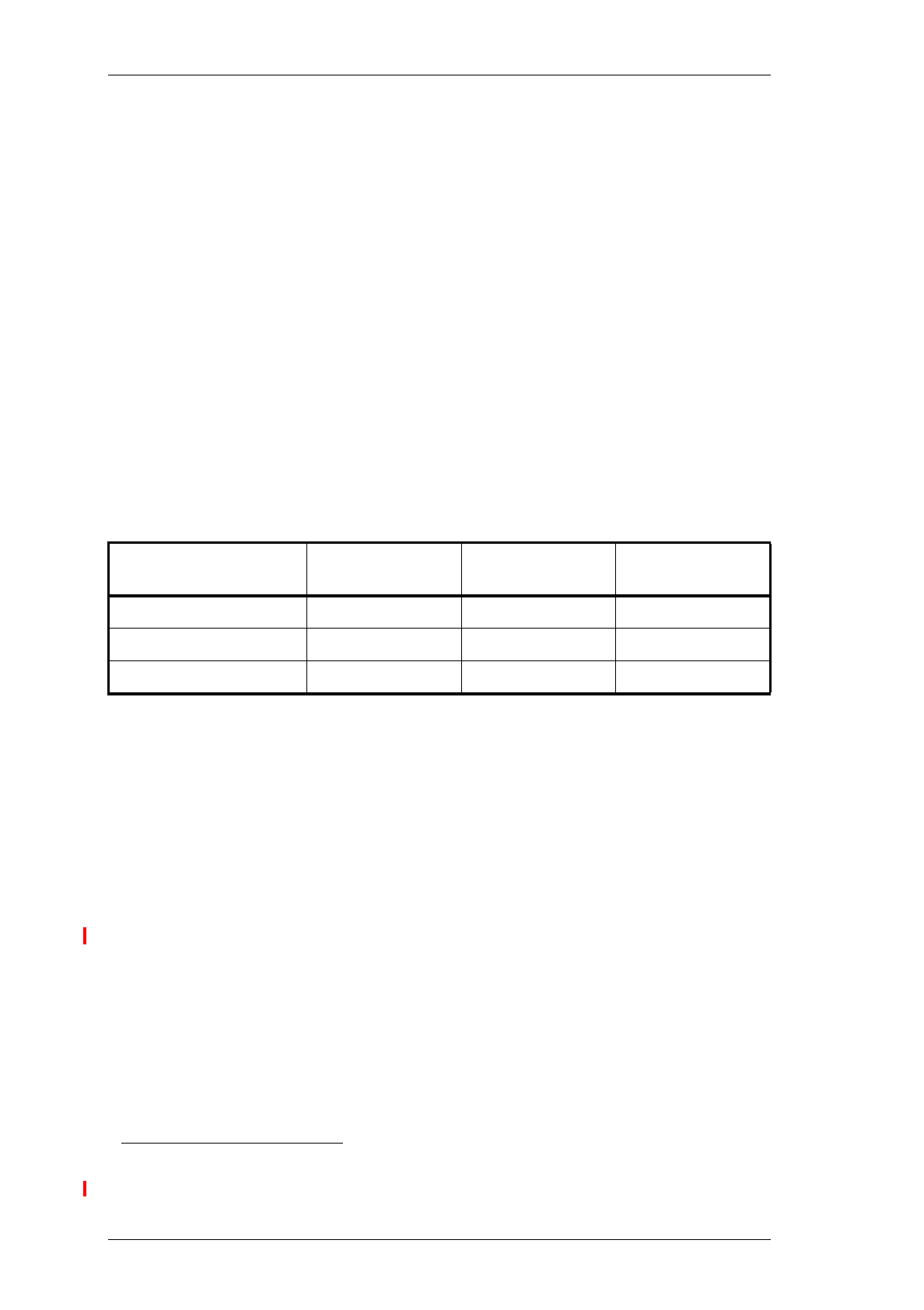
C1.8
T836/837 General Information
M830-00
23/07/99 Copyright TEL
1.2 Specifications
1.2.1 Introduction
The performance figures given are minimum figures, unless otherwise indicated, for
equipment tuned with the maximum switching range and operating at standard room
temperature (+22°C to +28°C) and standard test voltage (13.8V DC).
Where applicable, the test methods used to obtain the following performance figures are
those described in the EIA and ETS specifications. However, there are several parame-
ters for which performance according to the CEPT specification is given. Refer to Sec-
tion 1.2.6 for details of test standards.
Details of test methods and the conditions which apply for Type Approval testing in all
countries can be obtained from Tait Electronics Ltd.
The terms "wide bandwidth", "mid bandwidth" and "narrow bandwidth" used in this
and following sections are defined in the following table.
1.2.2 General
Number Of Channels .. 128 (standard)1
Supply Voltage:
Operating Voltage .. 10.8 to 16V DC
Standard Test Voltage .. 13.8V DC
Polarity .. negative earth only
Polarity Protection .. crowbar diode
Line Keying Supply (if required) .. -50V DC
Supply Current:
Transmit - T836 .. 4.5A (typical)
- T837 .. 600mA
Standby .. 150mA (typical)
Operating Temperature Range .. -30°C to +60°C
Channel Spacing Modulation
100% Deviation Receiver
IF Bandwidth
Wide Bandwidth 25kHz ±5.0kHz 15.0kHz
Mid Bandwidth 20kHz ±4.0kHz 12.0kHz
Narrow Bandwidth 12.5kHz ±2.5kHz 7.5kHz
1. Additional channels may be factory programmed. Contact your nearest Tait Dealer or
Customer Service Organisation.

M830-00
T836/837 General Information
C1.9
Copyright TEL 23/07/99
Dimensions:
Height .. 183mm
Width .. 60mm
Length .. 320mm
Weight .. 2.1kg
Time-Out Timer (optional) .. 0 to 5 minutes1 adjustable in 10 sec-
ond steps
Tail Timer .. 0 to 5 seconds adjustable in 100ms2
steps
Transmit Key Time .. <30ms
Transmit Lockout Timer .. 0 to 1 minute adjustable in 10 second
steps
1.2.3 RF Section
Frequency Range .. 136-174MHz (refer to Section 1.4 and
Section 1.5)
Modulation Type .. FM
Frequency Increment .. 5 or 6.25kHz
Switching Range .. 8MHz (i.e. ±4MHz from the centre
frequency)
Load Impedance .. 50 ohms
Frequency Stability .. ±2.5ppm, -30°C to +60°C
(see also Section 1.4 and Section 1.5)
Adjacent Channel Power (full deviation):
Wide Bandwidth (WB) .. -75dBc
(±25kHz/15kHz B/W)
Mid Bandwidth (MB) .. -70dBc
(±20kHz/12kHz B/W)
Narrow Bandwidth (NB) .. -65dBc
(±12.5kHz/7.5kHz B/W)
Transmitter Side Band Noise:
(no modulation, 15kHz bandwidth)
At ±25kHz .. -95dBc
At ±1MHz .. -105dBc
1. Adjustable from 0 to 10 minutes in PGM800Win version 2.12 and later.
2. Adjustable in 20ms steps in PGM800Win version 2.12 and later.

C1.10
T836/837 General Information
M830-00
23/07/99 Copyright TEL
Intermodulation .. -40dBc with interfering signal of
-30dBc
.. -70dBc with 25dB isolation
& interfering signal of -30dBc
(PA with output isolator)
T836 Mismatch Capability:
Ruggedness .. refer to your nearest Tait Dealer or
Customer Service Organisation
Stability .. 3:1 VSWR (all phase angles)
Radiated Spurious Emissions:
Transmit .. -36dBm to 1GHz
-30dBm to 4GHz
Standby .. -57dBm to 1GHz
-47dBm to 4GHz
Conducted Spurious Emissions: (T836 Only)
Transmit .. -36dBm to 1GHz
-30dBm to 4GHz
Standby .. -57dBm to 1GHz
-47dBm to 4GHz
Power Output:
T836 - Rated Power .. 25W
- Range Of Adjustment .. 5-25W
T837 .. 800mW ±200mW
Duty Cycle (T836 Only) .. 100% @ 25W at +25°C
.. 30% @ 25W at +60°C
.. 100% @ 10W at +60°C
1.2.4 Audio Processor
1.2.4.1 Inputs
Inputs Available .. line, microphone and CTCSS
Line Input:
Impedance .. 600 ohms (balanced)
Sensitivity (60% modulation @ 1kHz)-
With Compressor .. -50dBm
Without Compressor .. -30dBm
Microphone Input:
Impedance .. 600 ohms
Sensitivity (60% modulation @ 1kHz)-
With Compressor .. -70dBm
Without Compressor .. -50dBm

M830-00
T836/837 General Information
C1.11
Copyright TEL 23/07/99
1.2.4.2 Modulation Characteristics
Frequency Response .. flat or pre-emphasised (optional)
(below limiting)
Line And Microphone Inputs:
Pre-emphasised Response-
Bandwidth .. 300Hz to 3kHz (WB & MB)
.. 300Hz to 2.55kHz (NB)
Below Limiting .. within +1, -3dB of a 6dB/octave
pre-emphasis characteristic
Flat Response .. within +1, -2dB of output at 1kHz
Above Limiting Response .. within +1, -2dB of a flat response
(ref. 1kHz)
Distortion .. 2%
Hum And Noise:
Wide Bandwidth .. -55dB (300Hz to 3kHz [EIA]) typical
Mid Bandwidth .. -54dB (CEPT)
Narrow Bandwidth .. -50dB (CEPT)
Compressor (optional):
Attack Time .. 10ms
Decay Time .. 800ms
Range .. 50dB
1.2.4.3 CTCSS
Standard Tones .. all 37 EIA group A, B and C tones
plus 13 commonly used tones
Frequency Error .. 0.08% max.
(from EIA tones)
Generated Tone Distortion .. 1.2% max.
Generated Tone Flatness .. flat across 67 to 250.3Hz to within 1dB
Modulation Level .. adjustable
Modulated Distortion .. <5%
1.2.5 Microcontroller
Auxiliary Ports:
Open Drain Type .. capable of sinking 2.25mA via 2k2Ω
Vds max. .. 5V

C1.12
T836/837 General Information
M830-00
30/04/98 Copyright TEL
1.2.6 Test Standards
Where applicable, this equipment is tested in accordance with the following standards.
1.2.6.1 European Telecommunication Standard
ETS 300 086 January 1991
Radio equipment and systems; land mobile service; technical characteristics and test
conditions for radio equipment with an internal or external RF connector intended pri-
marily for analogue speech.
ETS 300 113 March 1996
Radio equipment and systems; land mobile service; technical characteristics and test
conditions for radio equipment intended for the transmission of data (and speech) and
having an antenna connector.
ETS 300 219 October 1993
Radio equipment and systems; land mobile service; technical characteristics and test
conditions for radio equipment transmitting signals to initiate a specific response in the
receiver.
ETS 300 279 February 1996
Radio equipment and systems; electromagnetic compatibility (EMC) standard for pri-
vate land mobile radio (PMR) and ancillary equipment (speech and/or non-speech).
1.2.6.2 DTI CEPT Recommendation T/R-24-01
Annex I: 1988
Technical characteristics and test conditions for radio equipment in the land mobile
service intended primarily for analogue speech.
Annex II: 1988
Technical characteristics of radio equipment in the land mobile service with regard to
quality and stability of transmission.
1.2.6.3 Telecommunications Industry Association
ANSI/TIA/EIA-603-1992
Land mobile FM or PM communications equipment measurement and performance
standards.

M830-00
T836/837 General Information
C1.13
Copyright TEL 23/07/99
1.3 Product Codes
The three groups of digits in the T830 Series II product code provide information about
the model, type and options fitted, according to the conventions described below.
The following explanation of T830 Series II product codes is not intended to suggest that
any combination of features is necessarily available in any one product. Consult your
nearest Tait Dealer or Customer Service Organisation for more information regarding
the availability of specific models, types and options.
Model
The Model group indicates the basic function of the product, as follows:
T83X-XX-XXXX T835 receiver
T836 25W transmitter
T837 exciter
T838 50W power amplifier
T839 100W power amplifier
Type
The Type group uses two digits to indicate the basic RF configuration of the product.
The first digit in the Type group designates the frequency range:
T83X-XX-XXXX ’1’ for 136-156MHz
’2’ for 148-174MHz
The second digit in the Type group indicates the channel spacing:
T83X-XX-XXXX ’0’ for wide bandwidth (25kHz)
’3’ for mid bandwidth (20kHz)
’5’ for narrow bandwidth (12.5kHz)
Options
T83X-XX-XXXX The Options group uses four digits and/or letters to indicate
any options that may be fitted to the product. This includes
standard options and special options for specific customers.
’0000’ indicates a standard Tait product with no options fitted.
The large number of options precludes listing them here.

C1.14
T836/837 General Information
M830-00
23/07/99 Copyright TEL
1.4 T836 Standard Product Range
The following table lists the range of standard T836 types (i.e. no options fitted) availa-
ble at the time this manual was published. Consult your nearest Tait Dealer or Cus-
tomer Service Organisation for more information.
You can identify the transmitter type by checking the product code printed on a label on
the rear of the chassis (Figure 1.1 in Part A shows typical labels). You can further verify
the transmitter type by checking the placement of an SMD resistor in the table that is
screen printed onto the PCB (refer to Section 6.1 for more details).
Frequency Range (MHz) 136-156
Deviation (kHz) 2.5 2.5 4 5
TCXOa
a. A TCXO with a stability of ±1ppm (0°C to +60°C) is available to suit specific
requirements. Contact your nearest authorised Tait Dealer or Customer
Service Organisation for further details.
±2.5ppm -30°C to +60°C • •••
Transmitter Type: T836- 16-0000b
b. United States market only.
15-0000 13-0000 10-0000
Frequency Range (MHz) 148-174
Deviation (kHz) 2.5 2.5 4 5
TCXOa±2.5ppm -30°C to +60°C • •••
Transmitter Type: T836- 26-0000b25-0000 23-0000 20-0000

M830-00
T836/837 General Information
C1.15
Copyright TEL 23/07/99
1.5 T837 Standard Product Range
The following table lists the range of standard T837 types (i.e. no options fitted) availa-
ble at the time this manual was published. Consult your nearest Tait Dealer or Cus-
tomer Service Organisation for more information.
You can identify the exciter type by checking the product code printed on a label on the
rear of the chassis (Figure 1.1 in Part A shows typical labels). You can further verify the
exciter type by checking the placement of an SMD resistor in the table that is screen
printed onto the PCB (refer to Section 6.1 for more details).
Frequency Range (MHz) 136-156
Deviation (kHz) 2.5 2.5 4 5
TCXOa
a. A TCXO with a stability of ±1ppm (0°C to +60°C) is available to suit specific
requirements. Contact your nearest authorised Tait Dealer or Customer
Service Organisation for further details.
±2.5ppm -30°C to +60°C • •••
Exciter Type: T837- 16-0000b
b. United States market only.
15-0000 13-0000 10-0000
Frequency Range (MHz) 148-174
Deviation (kHz) 2.5 2.5 4 5
TCXOa±2.5ppm -30°C to +60°C • •••
Exciter Type: T837- 26-0000b25-0000 23-0000 20-0000


M830-00
T836/837 Circuit Operation
C2.1
Copyright TEL 30/04/98
2 T836/837 Circuit Operation
This section provides a basic description of the circuit operation of the T836 transmitter
and T837 exciter.
Note:
Unless otherwise specified, the term "PGM800Win" used in this and follow-
ing sections refers to version 2.00 and later of the software.
Refer to Section 6 where the parts lists, grid reference index and diagrams will provide
detailed information on identifying and locating components and test points on the
main PCB. The parts list and diagrams for the VCO PCB are in Part E.
The following topics are covered in this section.
Section Title Page
2.1 Introduction 2.3
2.2 Microcontroller 2.4
2.3
2.3.1
Synthesised Local Oscillator
Two Point Modulation
2.5
2.6
2.4
2.4.1
VCO
VCO Supply
2.7
2.7
2.5
2.5.1
2.5.2
2.5.3
2.5.4
2.5.5
Audio Processor
General
Audio Inputs
Keying Inputs
Compressor (Automatic Level Control (ALC))
Outputs To Modulators
2.8
2.8
2.8
2.9
2.9
2.9
2.6 Power Supply & Regulator Circuits 2.10
2.7 Transmit Timers 2.11
2.8 T836 Drive Amplifier & PA 2.12
2.9 T837 Exciter Drive Amplifier 2.13

C2.2
T836/837 Circuit Operation
M830-00
30/04/98 Copyright TEL
Figure Title Page
2.1
2.2
2.3
2.4
2.5
2.6
2.7
2.8
T836 High Level Block Diagram
T837 High Level Block Diagram
T836/837 Microcontroller Block Diagram
T836/837 Synthesiser Block Diagram
T836/837 Two Point Modulation
T836/837 Audio Processor Block Diagram
T836/837 Power Supply & Regulators Block Diagram
T836/837 Transmit Timers
2.3
2.3
2.4
2.5
2.6
2.8
2.10
2.11
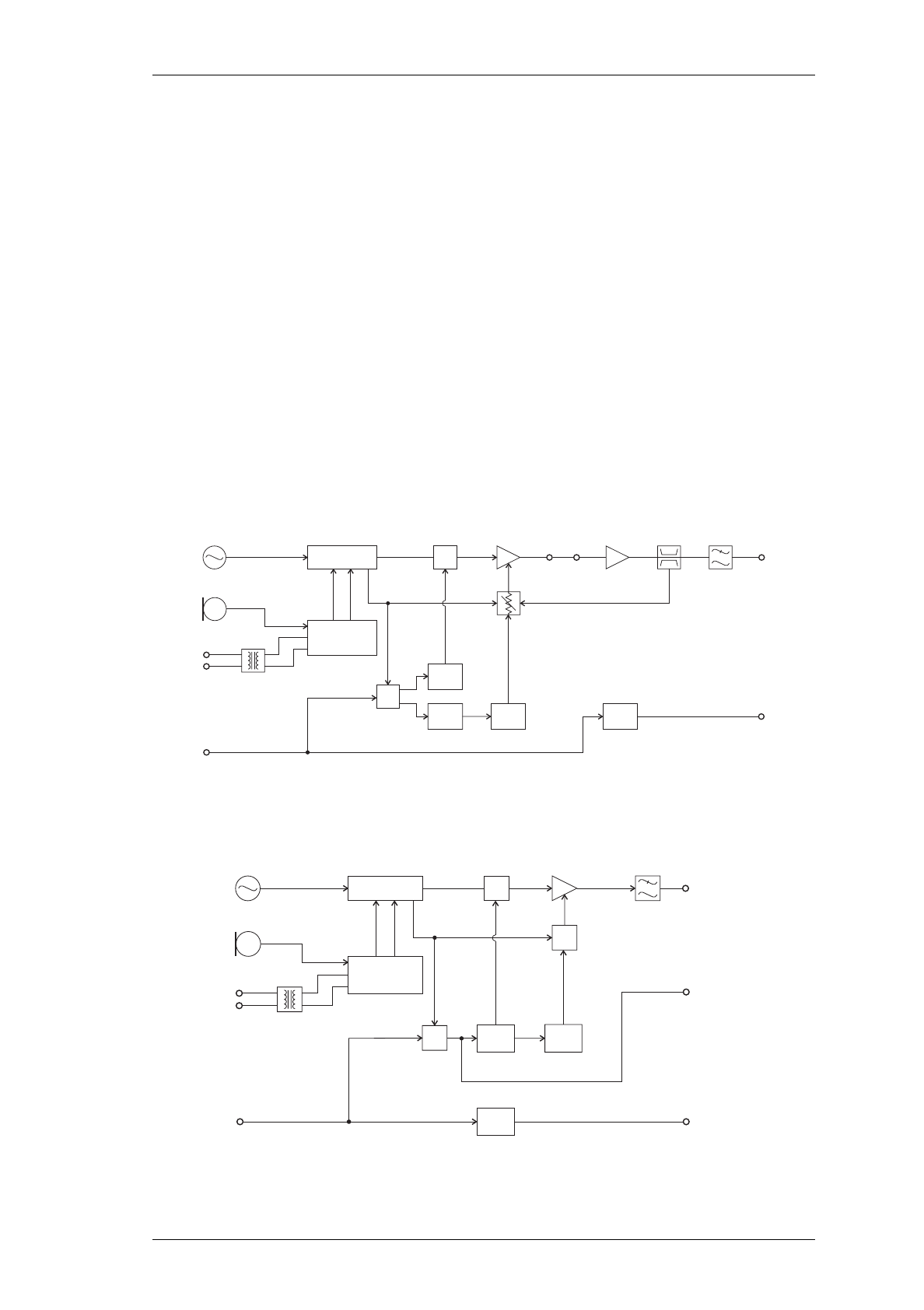
M830-00
T836/837 Circuit Operation
C2.3
Copyright TEL 30/04/98
2.1 Introduction
The individual circuit blocks which make up the T836 and T837 are:
• synthesiser
•VCO
• audio processor
• drive amplifier
• power amplifier (T836 only)
• voltage regulators.
Each of these circuit blocks is set in its own shielded compartment, formed as an inte-
gral part of the main chassis.
The configuration of the circuit blocks may be seen on a functional level in Figure 2.1
and Figure 2.2. Refer to the circuit diagrams in Section 6.2 (T836) or 6.3 (T837) for more
detail.
Figure 2.1 T836 High Level Block Diagram
Figure 2.2 T837 High Level Block Diagram
Ramp
Gen.
Time
Delay
Time
Delay
Time
Delay
Audio
Processor
Synthesiser +22dBm
Reference
Oscillator
12.8MHz
Microphone
Line
Transformer
Lock
Detect
PIN
Switch
Power
Control
Drive
Amp. PA
VCO
Gate
Directional
Coupler Low Pass
Filter
Exciter
Output
(+27dBm) Transmitter
Output
(25W)
Tx Reg
&
Audio
Processor
Synthesiser +22dBm
Reference
Oscillator
12.8MHz
Microphone
Line
Transformer
Lock
Detect
PIN
Switch
Switching
Control
Drive
Amp.
Gate
Exciter
Output
(800mW)
&Ramp
Gen.
Tx Reg VCO
Time
Delay
Time
Delay
Low Pass
Filter
PA Control Signal
(via exciter RF coax)
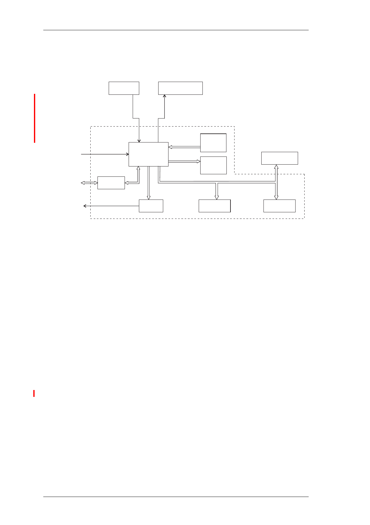
C2.4
T836/837 Circuit Operation
M830-00
23/07/99 Copyright TEL
2.2 Microcontroller
(Refer to the microcontroller circuit diagram (sheet 8) in Section 6.2 or 6.3.)
Figure 2.3 T836/837 Microcontroller Block Diagram
Overall system control of the T836/837 is accomplished by the use of a member of the
80C51 family of microcontrollers (IC810). It runs from internal ROM and RAM, thus
leaving all four ports free for input/output functions.
Non-volatile data storage is achieved by serial communication with a 16kBit EEPROM
(IC820). This serial bus is also used by the microcontroller to program the synthesiser
(IC740) and deviation control EPOTS (IC220).
The main tasks of the microcontroller are as follows:
• program the synthesiser and EPOT;
• interface with the PGM800Win programming software at 9600 baud via the
serial communication lines on D-range 1 (PL100) & D-range 2;
• monitor channel change inputs from D-range 2;
• generate timing waveforms for CTCSS encoding;
• coordinate and implement timing control of the exciter/transmitter;
• control the front panel "Supply" LED (refer to Section 5.3).
5V Reset
5V Digital
Regulator Watchdog
Reset
Channel
Select
Port
Auxiliary
Output
Port
Microcontroller
12.8MHz
Clock
Microcontroller Cavity
CTCSS Tone
External
Serial
Port
EEPROM Synthesiser
Dual Digital
Potentiometer
CTCSS
Encoder
Converter
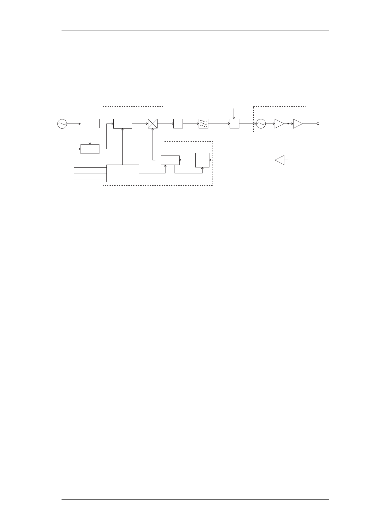
M830-00
T836/837 Circuit Operation
C2.5
Copyright TEL 30/04/98
2.3 Synthesised Local Oscillator
(Refer to the synthesiser circuit diagram (sheet 7) in Section 6.2 or 6.3 and the VCO cir-
cuit diagram in Part E.)
Figure 2.4 T836/837 Synthesiser Block Diagram
The synthesiser (IC740) employs a phase-locked loop (PLL) to lock a voltage controlled
oscillator (VCO) to a given reference frequency. The synthesiser receives the divider
information from the control microprocessor via a 3 wire serial bus (clock, data, enable).
When the data has been latched in, the synthesiser processes the incoming signals from
the VCO buffer (fin) and the phase modulator (fref).
A reference oscillator at 12.8MHz (IC700) is buffered (IC710 pins 3 & 4) and divided
down to 200kHz (IC730). This 200kHz square wave is then summed with the modulat-
ing audio and passed to an integrator (IC720 pins 9 & 8, Q710, Q720). This produces a
ramping waveform which is centred around a DC level determined by the incoming
audio. IC720 pins 5 & 6 perform as a comparator, ultimately producing a phase-modu-
lated 200kHz square wave. This is followed by another phase shifting stage (IC720 pins
3 & 4, Q730, Q740), before being divided down to 6.25kHz or 5kHz within the synthe-
siser IC (IC740).
A buffered output of the VCO (Q795) is divided with a prescaler and programmable
divider which is incorporated into the synthesiser chip (IC740). This signal is compared
with the phase modulated reference signal at the phase detector (also part of the synthe-
siser chip). The phase detector outputs drive a balanced charge pump circuit (Q760,
Q770, Q775, Q780, Q785) and active loop filter (IC750 pins 5, 6 & 7) which produces a
DC voltage between 0V and 20V to tune the VCO. This VCO control line is further fil-
tered to attenuate noise and other spurious signals. Note that the VCO frequency
increases with increasing control voltage.
If the synthesiser loop loses lock, a pulsed signal appears at LD (pin 2) of IC740. This
signal is filtered and buffered by IC750 pins 1, 2 & 3, producing the Lock-Detect signal
used to shut off the power supply to the drive amplifier. IC750 pin 1 is at 20V when the
synthesiser is out of lock.
/R
Reference
Divider
12.8MHz
Reference
Oscillator Fixed
Divider
/64
Phase
Modulator
Ref
Mod
Phase
Detector Charge
Pump Loop
Filter
FREQUENCY SYNTHESISER IC
Serial
Bus
Clk
Data
En Controller
/N
Programmable
Divider
64/65
Prescaler
VCO PCB
VCO
Modulation
VCO Buffer Output
Buffer
+22dB
m
L.O.
Divider Buffer
f
ref
f
in
Σ
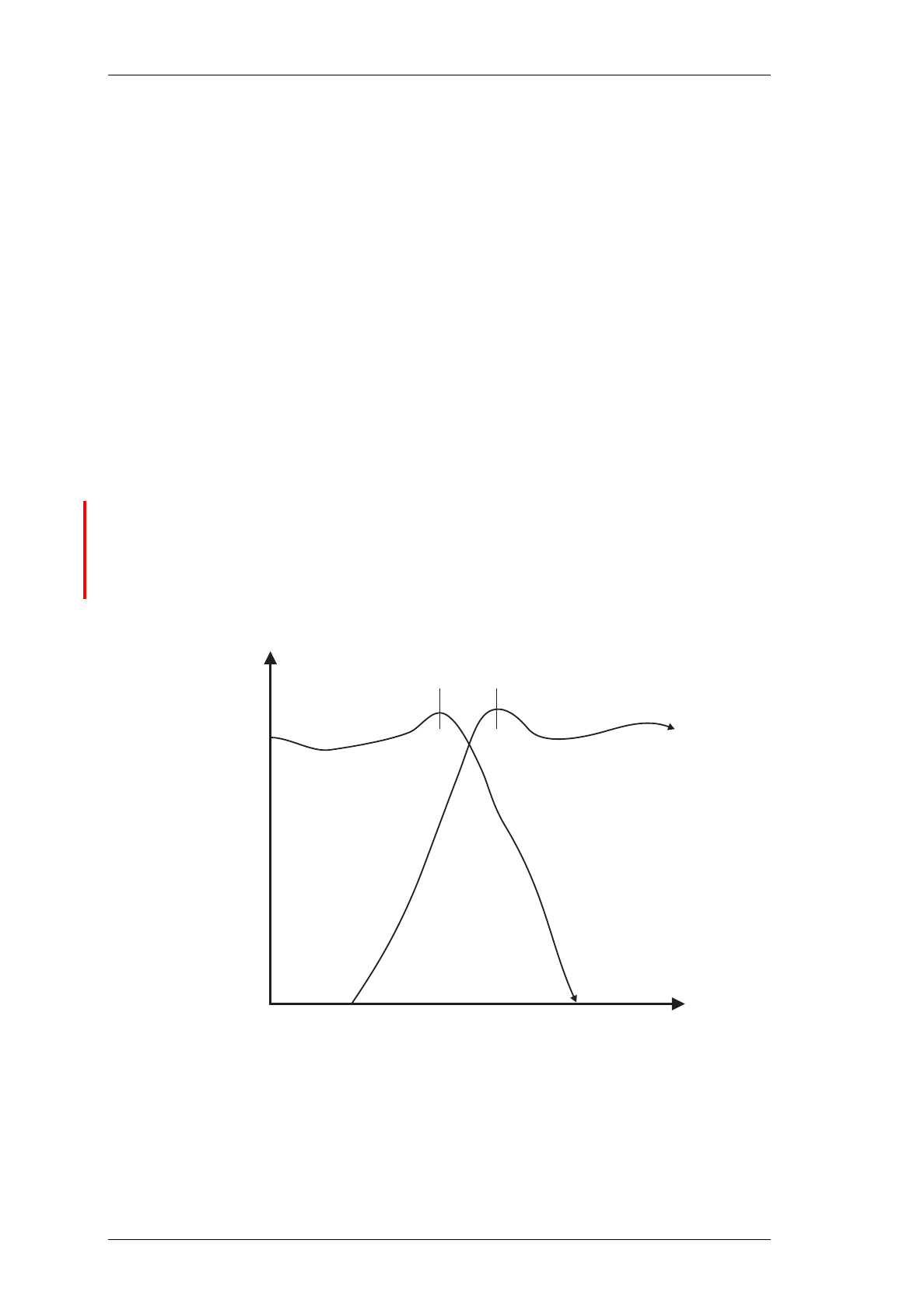
C2.6
T836/837 Circuit Operation
M830-00
23/07/99 Copyright TEL
2.3.1 Two Point Modulation
Frequency modulation occurs by modulating both the VCO input and the synthesiser
reference input. This process is called two point modulation and ensures a flat modula-
tion response from 67Hz to 3kHz (2.55kHz for narrow bandwidth).
The PLL has a fast response time, allowing a Tx key-up time of <30ms. Because of this
fast response time the PLL sees lower modulation frequencies superimposed on the
VCO as an error and corrects for it, resulting in no modulation on the carrier. At modu-
lation frequencies greater than 300Hz the loop cannot correct fast enough and modula-
tion is seen on the carrier. The response of the loop to VCO modulation is shown by f2
in Figure 2.5 below.
To achieve low frequency modulation, the reference oscillator is also modulated so that
the phase detector of IC740 detects no frequency error under modulation. Thus, the
synthesiser loop will not attempt to correct for modulation and the audio frequency
response of the transmitter remains unaffected. The response of the loop to reference
frequency modulation is shown by f1 in Figure 2.5.
The reference modulation is controlled by a 256-step 10k electronic potentiometer
(EPOT) which is adjustable via PGM800Win. The EPOT is made up of 256 resistive sec-
tions (representing approximately 39Ω each) which can be individually addressed by
the microcontroller. Each section can be switched in or out of circuit to achieve the
required total resistance, thus giving control of the reference modulation.
Figure 2.5 T836/837 Two Point Modulation
12
ff
TCXO VCO
Deviation
Frequency

M830-00
T836/837 Circuit Operation
C2.7
Copyright TEL 30/04/98
2.4 VCO
(Refer to the VCO circuit diagram in Part E.)
The VCO transistor (Q1) operates in a common source configuration, with an LC tank
circuit coupled between its gate and drain to provide the feedback necessary for oscilla-
tion. The VCO control voltage from the loop filter (IC750 pin 7) is applied to the vari-
caps (D1-D4) to facilitate tuning within an 8MHz band of frequencies. A trimcap (CV1)
is used for coarse tuning of the VCO. The output from the oscillator circuit drives a cas-
code amplifier stage (Q2, Q3) which supplies +10dBm (typically) to a further stage of
amplification, Q5. This is the final amplifier on the VCO PCB, and delivers +22dBm
(typically) to the exciter drive amplifier.
A low level "sniff" is taken from the output of Q3 and used to drive the divider buffer
(Q795) for the synthesiser (IC740).
The VCO operates at the actual output frequency of the exciter, i.e. there are no multi-
plier stages. The VCO is modulated by superimposing the audio signal onto the control
voltage and by phase modulating the reference signal.
2.4.1 VCO Supply
The VCO is supplied from two switched +9V supplies under the control of the Tx-Reg.
supply.
The VCO (Q1) and buffer amplifier (Q2 & Q3) are supplied from one +9V switched sup-
ply by Q540 via the capacitor multiplier (Q550, C550).
The output amplifier is supplied from the other +9V supply by Q520, Q530, and Q510.
A delay circuit holds the VCO on for a short time after the Tx-Reg. supply has been
switched off. This is to allow the RF power circuits (both exciter and PA) to ramp down
in the correct manner before the VCO is switched off.
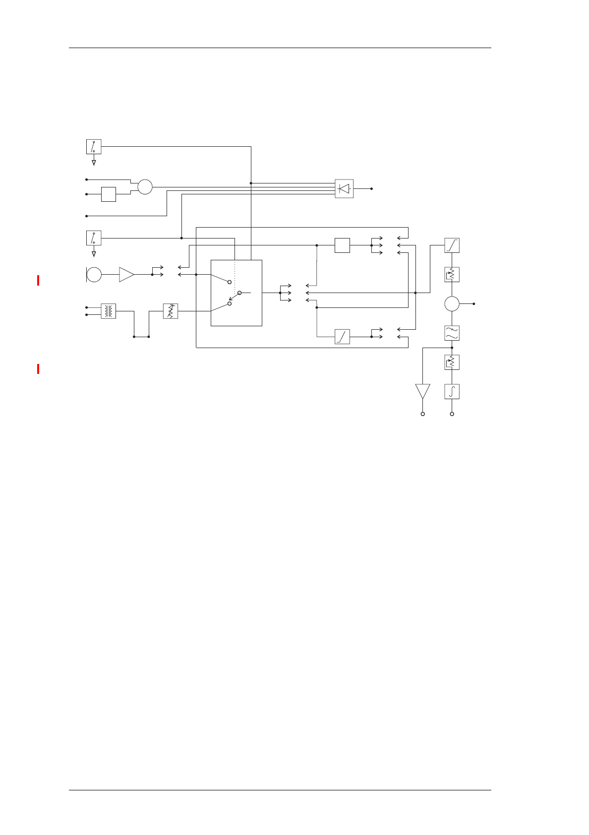
C2.8
T836/837 Circuit Operation
M830-00
23/07/99 Copyright TEL
2.5 Audio Processor
(Refer to the audio processor circuit diagram (sheet 2) in Section 6.2 or 6.3.)
Figure 2.6 T836/837 Audio Processor Block Diagram
2.5.1 General
The audio processor comprises several link selectable circuit blocks which may be con-
figured in a variety of combinations to suit individual requirements. The pre-emphasis
network and compressor may be linked individually or cascaded between either or both
audio inputs and the limiter.
Refer to Section 3.5.1 for linking details.
2.5.2 Audio Inputs
Two audio inputs are available: one from a 600 ohm balanced (or unbalanced) line, and
the other from a local microphone. The microphone signal is passed first to a pre-ampli-
fier (Q210) and ultimately to a multiplexer (IC240), but in between may pass through
the compressor (depending on the linking details). The line transformer is also con-
nected to the multiplexer and is disabled by the microphone PTT switch.
A third input for external CTCSS tones is also provided.
Pre-
emphasis
34
6
B
C
5
6
4
34
2
5
3
3
5
7
12
8
N
H
M
I
E
L
J
D
4
6
1
mic.
line
Multiplexer
Inputs
Output
Output
Inhibit
Audio 1 Audio 2
Compressor
Link
Link
Link
Tx Enable
Σ
Carrier
Opto-Key
Tx Key
PTT
Microphone
Input
Line Input
Microphone
Pre-amp.
Opto-coupler
Link
PL205
PL215
PL220
PL210
Limiter
Set Deviation
CTCSS
Low Pass
Filter
Ref. Mod. Adjust
Integrator
Digital Pot. (EPOT)
Digital Pot. (EPOT)
Buffer
Output
To VCO Ref.
Mod.
Constant Current Sink
+
_

M830-00
T836/837 Circuit Operation
C2.9
Copyright TEL 23/07/99
2.5.3 Keying Inputs
There are four ways to key the exciter:
• pulling the Tx-Key line low (pin 13 on D-range 1 [PL100]) at the rear of the set);
• pushing the "Carrier" button on the front panel - this will inhibit all audio;
• using the PTT button on the local microphone, disabling audio from the line;
• via the opto-key inputs (pins 11 and 12 on D-range 1 [PL100]) when electrical
isolation is required. This features a constant current sink (Q270) to ensure reli-
able activation of the opto-coupler (IC250) at low keying voltages.
2.5.4 Compressor (Automatic Level Control (ALC))
The input signal is fed via a current controlled attenuator (Q230, Q220) to a high gain
stage (IC230) from which the output signal is taken. This signal is passed to a compara-
tor (IC230) which toggles whenever the audio signal exceeds a DC threshold deter-
mined by RV220. Thus, the comparator produces a square wave whose mark-space
ratio is determined by the amplitude of the audio signal. This square wave pumps up
the reservoir capacitor (C233) which controls the attenuator (Q230, Q220), thus complet-
ing the feedback loop.
The compression level is set by adjustment of the comparator threshold (RV220).
Note:
Although the high dynamic range of the compressor allows the use of very
low audio signal levels, such conditions will be accompanied by a degrada-
tion of the signal-to-noise ratio. Very low audio input levels should there-
fore be avoided where possible.
2.5.5 Outputs To Modulators
The output signal from the limiter (IC210, IC230) is added with a CTCSS tone at a sum-
ming amplifier (IC260). The signal is then low pass filtered (IC260) and split to supply
the two modulators.
Since the VCO modulator is a true frequency modulator, its audio is simply buffered
(IC260). The reference modulator, however, is a phase modulator and its audio must
first be integrated (IC210).
It is vital that the audio levels to the modulators are accurately set, relative to each
other. Hence the inclusion of level adjustment in the reference modulator path. Once
set, adjustments to absolute deviation may be made only by IC220, a 256-step 10k elec-
tronic potentiometer (EPOT), which is controlled via PGM800Win. The EPOT is made
up of 256 resistive sections (representing approximately 39Ω each) which can be indi-
vidually addressed by the microcontroller. Each section can be switched in or out of cir-
cuit to achieve the required total resistance, thus adjusting the absolute deviation level.
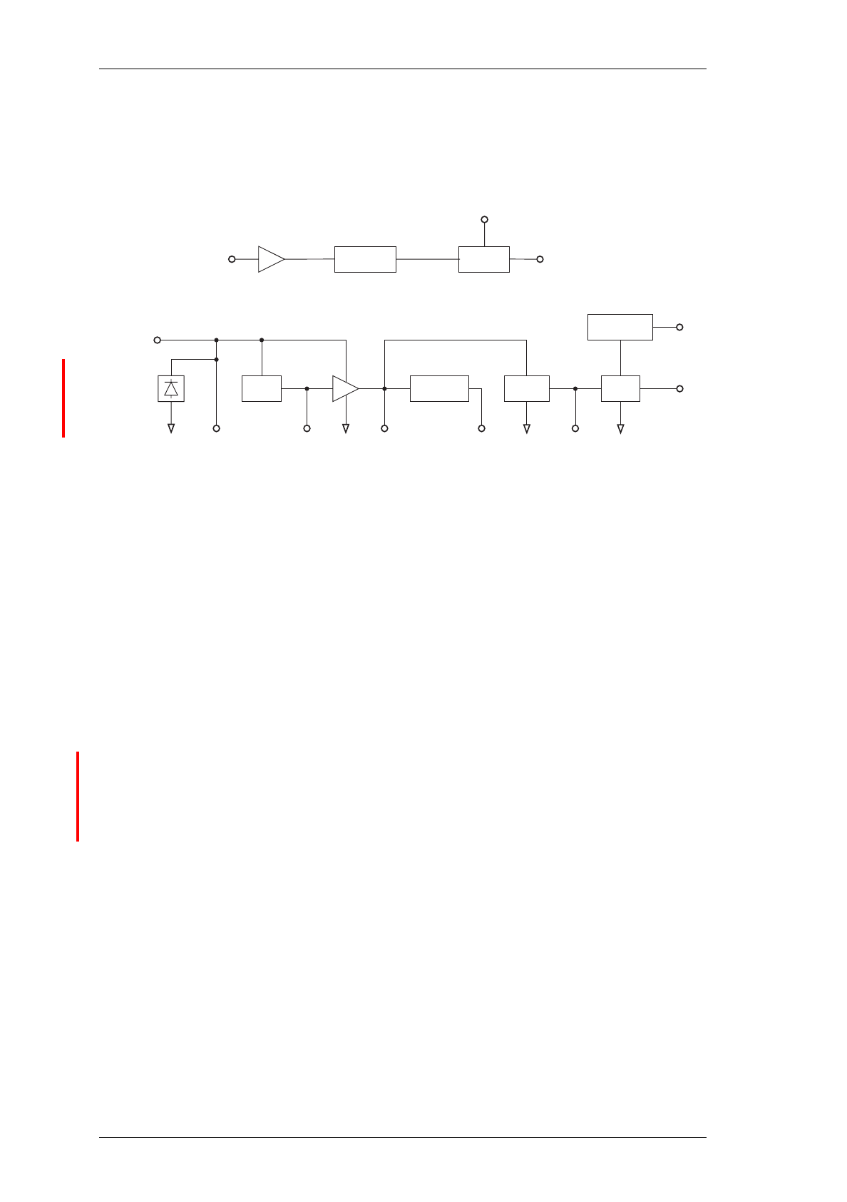
C2.10
T836/837 Circuit Operation
M830-00
23/07/99 Copyright TEL
2.6 Power Supply & Regulator Circuits
(Refer to the regulators circuit diagram (sheet 6) in Section 6.2 or 6.3.)
Figure 2.7 T836/837 Power Supply & Regulators Block Diagram
The T836 and T837 are designed to operate from a 10.8-16V DC supply (13.8V nominal).
A 5.3V regulator (IC630) runs directly from the 13.8V rail, driving much of the synthe-
siser circuitry. It is also used as the reference for a DC amplifier (IC640, Q630, Q620)
which provides a medium current capability 9V supply.
A switching power supply (Q660, Q670) runs from the 9V supply and provides a low
current capability +20V supply. This is used to drive the synthesiser loop filter (IC750),
giving a VCO control voltage range of up to 20V, and the Lock-Detect amplifiers.
Ultimate control of the transmitter is via the Tx-Reg. supply, switched from 9V by Q610.
This is enabled via the Tx-Enable signal from the audio processor, and microprocessor.
A crowbar diode is fitted for protection against connection to a power supply of incor-
rect polarity. It also provides transient overvoltage protection.
Note:
A fuse must be fitted in the power supply line for the diode to provide effec-
tive protection.
Crowbar
Diode LVI
5V
Reg
DC
Amp Switching
PS 5V Dig
Reg
Power
Switch
13.8V
Nom. 5V 5V Dig9V 20V
13.8V Nom.
From Rear
D-Range
Tx Enable
Buffer
Tx Reg.
+9V
µP
Watchdog
Timer
Micro-
controller
µP
Reset
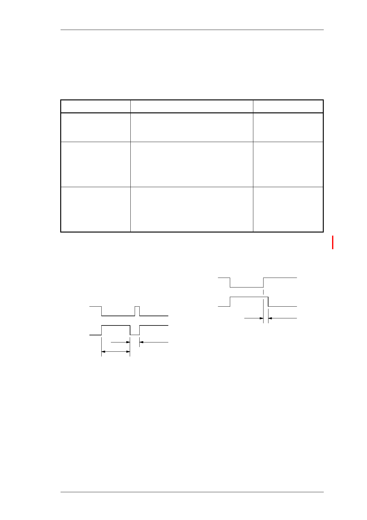
M830-00
T836/837 Circuit Operation
C2.11
Copyright TEL 23/07/99
2.7 Transmit Timers
The transmit tail timer, transmit timeout timer and transmit lockout timer can all be set
from PGM800Win. The fields for setting these are found on the system information
page. These three timers operate as follows (refer also to Figure 2.8):
Figure 2.8 T836/837 Transmit Timers
Timer Function Adjustment
Transmit Tail Sets the tail time during which the
transmitter stays keyed after the exter-
nal key source has been removed.
0-5 seconds in 100ms
stepsa
a. Adjustable in 20ms steps in PGM800Win version 2.12 and later.
Transmit Timeout Sets the maximum continuous trans-
mission time. Once the timer has
timed out, the transmitter must be
keyed again, unless prevented by the
transmit lockout timer.
0-300 secondsb in 10
second steps
b. Adjustable from 0 to 600 seconds in PGM800Win version 2.12 and later.
Transmit Lockout Sets the period of time that must
elapse after a timeout before the trans-
mitter can re-transmit. Once the timer
has timed out, the transmitter can be
keyed again.
0-60 seconds in 10
second steps
On
Lockout Time
Timeout
Time
On
Tail Time
Tx-Enable
Tx-Reg.
Tx-Enable
Tx-Reg.

C2.12
T836/837 Circuit Operation
M830-00
30/04/98 Copyright TEL
2.8 T836 Drive Amplifier & PA
(Refer to Figure 2.1 and the exciter and PA circuit diagrams (sheets 3 & 4) in Section 6.2.)
The output power of the PA is maintained at a constant level via a power control loop
applied to the two-stage, wide band exciter amplifier (Q365, Q370). The forward and
reverse RF power levels are sensed via a dual directional coupler and detector diodes
(D410, D420 in the PA cavity). The detected DC signals are summed with the ’power
adjust’ level and fed to the control integrator (IC330 pins 1, 2 & 3). The output control
voltage is buffered by Q310 and Q315, and applied to the collectors of the wide band
exciter amplifier.
Note:
Forward and reflected power signals are summed so that, under high
VSWR, the power control will turn the output RF level down.
To reduce the spurious output level when the synthesiser is out-of-lock, the Tx-Reg. and
Lock-Detect signals are gated to inhibit the PA control circuit and to switch off the RF
signal at the input to the drive amplifier. This is achieved by a PIN switch attenuator
(D340, D350, D360).
Cyclic keying control is provided by additional circuitry consisting of several time
delay, ramp and gate stages:
• Q350, Q355, Q360, IC330 pins 1, 2 & 3 power ramping
• Q340, Q345 Tx-Reg. and Lock-Detect gate
• Q320, Q325, Q330, Q335 delay and PIN switch drive.
This is to allow the RF power circuits (both exciter and PA) to ramp up and down in a
controlled manner so that minimal adjacent channel interference is generated during
the transition.
The output of the wide band amplifier is approximately 500mW (+27dBm) for an input
of 170mW (+22dBm) when the power control is set to maximum.
The zener diode (D330) limits the upper range of the controlled voltage to the exciter
transistors.
A temperature sensor (R460) is provided so that the RF output power can be reduced to
a preset level when a set temperature is exceeded. This is a protection circuit (IC330
pins 5, 6 & 7, Q305) to prevent overheating, as the unit is not rated for continuous oper-
ation at high temperatures (refer to Section 1.2.3 for duty cycle specifications). RV330
sets the PA output power while under high temperature fold-back conditions.
R359, R360 and R362 form a 6dB attenuator to provide good VCO/exciter isolation.
The output attenuator (R392, R390, R394 and R396) aids in reducing exciter/PA interac-
tion while also ensuring a reasonable match for Q350.
The RF output from the exciter is fed to the driver stage (Q415) and then to the final
(Q425). DC is fed to the final via a low pass filter with special low frequency decou-
pling. CV451 tunes the output matching across the entire band.

M830-00
T836/837 Circuit Operation
C2.13
Copyright TEL 30/04/98
2.9 T837 Exciter Drive Amplifier
(Refer to Figure 2.2 and the exciter circuit diagram (sheet 3) in Section 6.3.)
A two-stage, wide band amplifier (Q365, Q370) provides an output level of approxi-
mately 800mW (+29dBm) for an input of 170mW (+22dBm) from the VCO. IC330 pins
5, 6 & 7, Q310, and Q315 provide a 10.5V regulated supply for the exciter.
To reduce the spurious output level when the synthesiser is out-of-lock, the Tx-Reg. and
Lock-Detect signals are gated to inhibit the exciter control circuit and to switch off the
RF signal at the input to the drive amplifier. This is achieved by a PIN switch attenuator
(D340, D350, D360).
Cyclic keying control is provided by additional circuitry consisting of several time
delay, ramp and gate stages:
• Q305, IC330 pins 5, 6 & 7 power ramping
• Q340, Q345 Tx-Reg. and Lock-Detect gate
• Q320, Q325, Q330, Q335 delay and PIN switch drive.
This is to allow the RF power circuits (both exciter and PA) to ramp up and down in a
controlled manner so that minimal adjacent channel interference is generated during
the transition.
R359, R360 and R362 form a 6dB attenuator to provide good VCO/drive amplifier isola-
tion.
The output attenuator (R392, R390, R394, R396) assists in reducing exciter/PA interac-
tion while also ensuring a good match for Q370.
Note:
The exciter provides a DC control signal to the PA via the RF coax. This is
injected via L390.


M830-00
T836/837 Initial Tuning & Adjustment
C3.1
Copyright TEL 23/07/99
3 T836/837 Initial Tuning & Adjustment
Caution:
This equipment contains CMOS devices which are susceptible to dam-
age from static charges. Refer to Section 1.2 in Part A for more infor-
mation on anti-static procedures when handling these devices.
The following section describes both short and full tuning and adjustment procedures
and provides information on:
• channel programming
• selecting required audio links
• synthesiser alignment
• PA alignment (T836 only)
• modulator adjustment
• limiter adjustment
• setting line level
• compressor adjustment
• timer adjustment.
Note:
Unless otherwise specified, the term "PGM800Win" used in this and follow-
ing sections refers to version 2.00 and later of the software.
Refer to Figure 4.4 and Figure 4.5 which show the location of the main tuning and
adjustment controls. Refer also to Section 6 where the parts lists, grid reference index
and diagrams will provide detailed information on identifying and locating compo-
nents and test points on the main PCB. The parts list and diagrams for the VCO PCB are
in Part E.
Section Title Page
3.1 Introduction 3.3
3.2 Channel Programming 3.3
3.3 Test Equipment Required 3.4
3.4
3.4.1
3.4.2
3.4.3
3.4.4
3.4.5
3.4.6
3.4.7
Short Tuning Procedure
Introduction
Synthesiser Alignment
Output Power Adjustment (T836 Only)
Two Point Modulation Adjustment
CTCSS Encoder (If Used)
FM Deviation (Limiter) Adjustment
Line-in Level Adjustment
3.5
3.5
3.5
3.5
3.6
3.7
3.7
3.7

C3.2
T836/837 Initial Tuning & Adjustment
M830-00
23/07/99 Copyright TEL
3.5
3.5.1
3.5.2
Audio Processor Links
Link Details
Typical Options
3.8
3.8
3.8
3.6 Synthesiser Alignment 3.9
3.7 PA Alignment (T836 Only) 3.10
3.8 Thermal Shutdown (T836 Only) 3.10
3.9
3.9.1
3.9.2
3.9.3
3.9.4
3.9.5
3.9.6
3.9.6.1
3.9.6.2
3.9.6.3
Audio Processor
Two Point Modulation
Modulator Adjustment
CTCSS Encoder (If Used)
Limiter Adjustment
Line Level Without Compressor
Compressor
Compressor On Line Input Only
Compressor On Microphone Input Only
Compressor On Both Line & Microphone Inputs
3.11
3.11
3.11
3.12
3.12
3.12
3.13
3.13
3.13
3.14
Figure Title Page
3.1
3.2
T836/837 Test Equipment Set-up With T800-01-0010
T836/837 Test Equipment Set-up Without T800-01-0010
3.4
3.4
Section Title Page

M830-00
T836/837 Initial Tuning & Adjustment
C3.3
Copyright TEL 23/07/99
3.1 Introduction
When you receive your T836 transmitter or T837 exciter it will be run up and working
on a particular frequency (the "default channel")1. If you want to switch to a frequency
that is within the 8MHz switching range (i.e. ±4MHz from the factory programmed fre-
quency), you should only need to reprogram the transmitter/exciter with the
PGM800Win software (refer to the PGM800Win programming kit and Section 3.2
below).
However, if you want to switch to a frequency outside the 8MHz switching range, you
will have to reprogram and re-tune the transmitter/exciter to ensure correct operation.
In this case you should carry out the short tuning procedure described in Section 3.4.
If you have carried out repairs or other major adjustments, you must carry out the full
tuning and adjustment procedure described in this section (except for Section 3.4).
3.2 Channel Programming
You can program up to 128 channel frequencies into the transmitter/exciter’s EEPROM
memory (IC820) by using the PGM800Win software package and an IBM PC. You can
also use PGM800Win to select the transmitter/exciter’s current operating frequency (or
"default channel").
If the transmitter/exciter is installed in a rack frame, you can program it via the pro-
gramming port in the speaker panel. However, you can also program the transmitter/
exciter before it is installed in a rack frame as follows:
• by using a T800-01-0010 calibration test unit;
• via D-range 1;
• via D-range 2 (standard T800-03-0000 auxiliary D-range only);
• via SK805 (internal Micromatch connector).
If you do not use the T800-01-0010, you will have to connect the PC to the transmitter/
exciter via a module programming interface (such as the T800-01-0004).
For a full description of the channel programming procedure, refer to the PGM800Win
programming software user’s manual.
Note:
When an auxiliary D-range kit (D-range 2 - T800-03-0000) is fitted, you can
also select a channel with an external switch, such as the DIP switch on the
rack frame backplane PCB. Refer to Part C in the T800 Series Ancillary
Equipment Service Manual (M800-00-101 or later issue) or consult your
nearest Tait Dealer or Customer Service Organisation for further details.
1. Use the "Read Module" function in PGM800Win to find out what the default channel is.
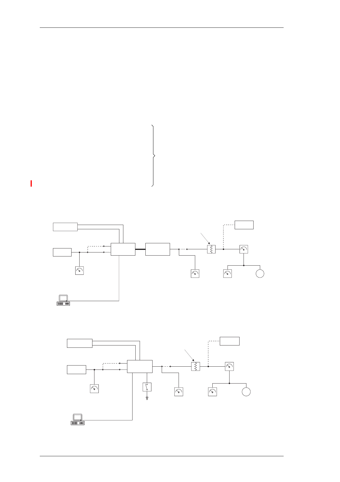
C3.4
T836/837 Initial Tuning & Adjustment
M830-00
23/07/99 Copyright TEL
3.3 Test Equipment Required
You will need the following test equipment:
• computer with PGM800Win installed
• T800 programming kit
• module programming interface (e.g. T800-01-0004 - optional)
• 13.8V power supply
• digital multimeter
• audio signal generator
• RF power meter
• audio voltmeter x 2
• modulation meter
• oscilloscope (digital preferred)
• 20dB or 40dB pad
• T800-01-0010 calibration test unit (optional)
Figure 3.1 and Figure 3.2 show typical test equipment set-ups.
Figure 3.1 T836/837 Test Equipment Set-up With T800-01-0010
Figure 3.2 T836/837 Test Equipment Set-up Without T800-01-0010
or RF test set (optional)
Frequency
Counter
Audio
Voltmeter
RF Power
Meter Oscilloscope
AF O/P
Modulation
Meter
20dB pad: exciter
40dB pad: transmitter
RF O/P
PGM800Win
PSU
+13.8V
-Ve
Audio
Generator
Line I/P
CTCSS I/P
Ω600
Audio
Voltmeter
Exciter/
Transmitter
T800
Calibration
Test Unit
PGM800Win
Serial
Com
PSU
+13.8V
-Ve
Frequency
Counter
Audio
Voltmeter
RF Power
Meter Oscilloscope
AF O/P
Modulation
Meter
20dB pad: exciter
40dB pad: transmitter
Audio
Generator
Line I/P
CTCSS I/P
Ω600
Audio
Voltmeter
Key
RF O/P
Exciter/
Transmitter
via module programming interface
(e.g. T800-01-0004)

M830-00
T836/837 Initial Tuning & Adjustment
C3.5
Copyright TEL 30/04/98
3.4 Short Tuning Procedure
Use this procedure only if you want to reprogram the T836/837 to a frequency outside
the 8MHz switching range and do not intend to carry out any other major adjustments
or repairs.
3.4.1 Introduction
Reprogram the operating frequency as described in the PGM800Win program-
ming kit (refer to Section 3.2).
Remove the top cover (nearest the handle).
Set up the test equipment as described in Section 3.3.
Set the links in the audio processor section as required (refer to Section 3.5).
3.4.2 Synthesiser Alignment
• Connect a high impedance voltmeter to PL4-1 or the junction of L1 & R1 in the
VCO (this measures the synthesiser loop voltage).
• Key the transmitter by earthing the Tx-Key line.
•Single Channel Tune VCO trimmer CV1 for a synthesiser loop voltage of
9V.
Multichannel Tune VCO trimmer CV1 for a synthesiser loop voltage of
9V on the middle channel.
If there is no middle channel, tune CV1 so that the chan-
nels are symmetrically placed around a loop voltage of 9V.
All channels should lie within the upper and lower limits
of 13V and 5V respectively.
Do not attempt to program channels with a greater fre-
quency separation than the specified switching range of
8MHz.
3.4.3 Output Power Adjustment (T836 Only)
Connect an RF power meter to the output socket and key the transmitter.
Turn RV320 (power adjust) fully clockwise.
Tune CV451 (output power trim) for maximum output power and check that this
is >30W.
Adjust RV320 for the required output power (between 5 and 25W).
Readjust CV451 to reduce the supply current by up to 0.5A.

C3.6
T836/837 Initial Tuning & Adjustment
M830-00
23/07/99 Copyright TEL
3.4.4 Two Point Modulation Adjustment
Note 1:
In this and following sections deviation settings are given first for wide
bandwidth sets, followed by settings in brackets for mid bandwidth sets ( )
and narrow bandwidth sets [ ].
Note 2:
The reference modulation and limiter adjustments are controlled by 256-
step electronic potentiometers (EPOTs), which are adjusted via the “Refer-
ence Modulation” and “Deviation” settings in PGM800Win. This allows the
two point modulation and deviation settings to be adjusted for each chan-
nel.
Note 3:
To optimise the modulation response across the switching range, repeat
steps 1-4 below for each channel that will be used (usually needed only for
data applications). In applications where the modulation response is less
critical (e.g. voice use only), carry out steps 1-4 below on the middle channel
and use the “EPOT Fill” option1 in PGM800Win to copy the value to the
other channels.
1. Inject an audio signal of 600Hz 1.5V rms (+5dBm) into the CTCSS input (D-range
1 (PL100) pin 8).
Key the transmitter by earthing the Tx-Key line.
2. Adjust the output from the audio generator to obtain ±3kHz (±2.4kHz) [±1.5kHz]
deviation at 600Hz.
3. Change the input frequency to 120Hz and, using PGM800Win, adjust the value of
the “Reference Modulation” EPOT setting for the current channel to obtain ±3kHz
(±2.4kHz) [±1.5kHz] deviation (you can use either the mouse or up and down
arrow keys).
4. Change the input frequency back to 600Hz.
Repeat steps 2 and 3 above until the deviations achieved at the two input frequen-
cies are within 0.2dB of each other. You will need to do this at least four times.
5. Sweep the audio between 50 and 300Hz for peaks.
Note:
A peak between 50 and 300Hz will indicate a fault condition, i.e:
- incorrect set-up
or - modulation circuitry fault.
The specification window is ±1dB relative to 150Hz from 65 to 260Hz.
1. Use the “EDIT FILL” button on the tool bar or go to “Edit”, “Fill”, “Epot Settings” on
the menu bar.

M830-00
T836/837 Initial Tuning & Adjustment
C3.7
Copyright TEL 23/07/99
3.4.5 CTCSS Encoder (If Used)
Program a CTCSS tone on the default channel using PGM800Win.
If you are using an RF test set, turn off the 300Hz high pass filter.
Key the T836/837 with the front panel "Carrier" switch.
Adjust RV805 (CTCSS level adjust) to give ±500Hz (±350Hz) [±250Hz] deviation.
Set the maximum deviation as per Section 3.4.6.
3.4.6 FM Deviation (Limiter) Adjustment
Note:
If the T836/837 will be used over the whole 8MHz switching range, you
must set the deviation for each channel. However, if the module will be
used on frequencies that cover only a 1MHz (or less) switching range, you
can set the deviation on the middle channel and use this value for all other
channels with the “EPOT Fill” option in PGM800Win.
Inject 1kHz at -10dBm into the line input (D-range 1 (PL100) pins 1 & 4; pins 2 & 3
shorted; refer to Section 2.2 of Part F).
Adjust RV210 (line sensitivity) fully clockwise and key the transmitter by earthing
the Tx-Key line. Using PGM800Win, adjust the value of the “Deviation” EPOT
setting for the current channel to obtain a deviation limit of ±4.7kHz (±3.8kHz)
[±2.3kHz] (you can use either the mouse or up and down arrow keys).
Sweep the audio frequency from 100Hz to 4kHz and ensure that the maximum
deviation does not exceed ±4.7kHz (±3.8kHz) [±2.3kHz]. Readjust “Deviation” if
necessary via PGM800Win.
3.4.7 Line-in Level Adjustment
Remove the CTCSS signal (if used).
Set the injected signal at the line input to the required line level (typically -10 to
-20dBm).
Adjust RV210 (line sensitivity) to provide ±3kHz (±2.4kHz) [±1.5kHz] deviation.
Reapply the CTCSS signal (if required).

C3.8
T836/837 Initial Tuning & Adjustment
M830-00
30/04/98 Copyright TEL
3.5 Audio Processor Links
3.5.1 Link Details
Use the following table to set up the audio processor to the configuration you require.
You should set the audio processor links before carrying out any of the tuning and
adjustment procedures. The factory settings are shown in brackets [ ].
3.5.2 Typical Options
Plug Linka
a. The letters in this column and in the table in Section 3.5.2 below refer to the identification
letters screen printed onto the PCB beside each pair of pins.
Function
PL205
1-2
[3-4]
5-6
A
B
C
not connected
microphone pre-amp. output to compressor input
microphone pre-amp. output to multiplexer input
PL210
[1-2]
3-4
5-6
L
M
N
multiplexer output to pre-emphasis input
multiplexer output to limiter input
multiplexer output to compressor input
PL215
1-2
[3-4]
5-6
7-8
9-10
G
H
I
J
K
not connected
compressor output to multiplexer input
compressor output to limiter input
compressor output to pre-emphasis input
not connected
PL220
1-2
[3-4]
5-6
D
E
F
pre-emphasis output to multiplexer input
pre-emphasis output to limiter input
not connected
PL205 PL210 PL215 PL220
microphone pre-amp. compressed
and pre-emphasised;
line input pre-emphasised
(standard set-up)
[3-4]
B
[1-2]
L
[3-4]
H
[3-4]
E
microphone pre-amp. compressed
and pre-emphasised;
line input unprocessed
3-4
B
3-4
M
7-8
J
1-2
D
line and microphone compressed
and pre-emphasised
5-6
C
5-6
N
7-8
J
3-4
E
microphone pre-amp. compressed;
line and microphone flat response
3-4
B
3-4
M
3-4
H
5-6
F

M830-00
T836/837 Initial Tuning & Adjustment
C3.9
Copyright TEL 23/07/99
3.6 Synthesiser Alignment
• Ensure that the T836/837 has been programmed with the required frequencies
using PGM800Win software.
•Single Channel Select a channel using PGM800Win.
Multichannel Select the middle channel via PGM800Win.
• Connect a high impedance voltmeter to PL4-1 or the junction of L1 and R1 in the
VCO (this measures the synthesiser loop voltage).
• Key the transmitter by earthing the Tx-Key line.
Single Channel Tune VCO trimmer CV1 for a synthesiser loop voltage of
9V.
Multichannel Tune VCO trimmer CV1 for a synthesiser loop voltage of
9V on the middle channel.
If there is no middle channel, tune CV1 so that the chan-
nels are symmetrically placed around a loop voltage of 9V.
All channels should lie within the upper and lower limits
of 13V and 5V respectively.
Do not attempt to program channels with a greater fre-
quency separation than the specified switching range
(8MHz).
• Check that the exciter output power is:
T836 500mW +200, -100mW (measured at SK310 in the exciter section)
T837 800mW ±200mW (measured at the rear panel N-type connector).
• Measure the exciter output frequency and adjust the TCXO (=IC700) trimmer if
required.
Caution:
This trimmer is susceptible to physical damage. Do not exert a down-
ward force of more than 500g (1lb) when adjusting.

C3.10
T836/837 Initial Tuning & Adjustment
M830-00
30/04/98 Copyright TEL
3.7 PA Alignment (T836 Only)
Check that the exciter is connected to the PA with the coaxial link.
Connect an RF power meter to the PA output.
Turn RV320 (power adjust) fully clockwise.
Measure and record the voltage (VL) at L490; perform this measurement at room
temperature so that the NTC (R460) is close to 25°C.
Key the transmitter by earthing the Tx-Key line.
Tune CV451 until maximum power is obtained.
Reduce the current by approximately 1A by detuning CV451 or until the power
drops below 30W.
Check that the total current drawn is less than 4.5A for 25W output power.
Adjust RV320 for an output power between 5 and 25W.
3.8 Thermal Shutdown (T836 Only)
Key the transmitter by earthing the Tx-Key line and set the output power to 25W
as described in Section 3.7.
Short L490 to ground.
Set RV330 (high temperature power adjust) for an output power of 5W.
Set RV310 (temperature adjust) to 0.16VL volts (measured at IC330 pin 5), where
VL is the voltage measured at L490 in Section 3.7. This sets the thermal shutdown
at 85°C at NTC R460.

M830-00
T836/837 Initial Tuning & Adjustment
C3.11
Copyright TEL 23/07/99
3.9 Audio Processor & CTCSS
3.9.1 Two Point Modulation
The T836 and T837 utilise two point modulation to obtain a wide audio bandwidth
independent of the synthesiser loop filter response. This is achieved by simultaneously
frequency modulating the VCO and phase modulating the synthesiser reference fre-
quency. The relative signal levels fed to the two modulators are quite critical and cause
interaction when setting up.
Both modulating signals require readjustment when the exciter is shifted in frequency
greater than the switching range (i.e. ∆F>±4MHz).
Note 1:
In this and following sections deviation settings are given first for wide
bandwidth sets, followed by settings in brackets for mid bandwidth sets ( )
and narrow bandwidth sets [ ].
Note 2:
The reference modulation and limiter adjustments are controlled by 256-
step electronic potentiometers (EPOTs), which are adjusted via the “Refer-
ence Modulation” and “Deviation” settings in PGM800Win. This allows the
two point modulation and deviation settings to be adjusted for each chan-
nel.
Note 3:
To optimise the modulation response across the switching range, repeat
steps 1-4 below for each channel that will be used (usually needed only for
data applications). In applications where the modulation response is less
critical (e.g. voice use only), carry out steps 1-4 below on the middle channel
and use the “EPOT Fill” option1 in PGM800Win to copy the value to the
other channels.
3.9.2 Modulator Adjustment
1. Inject an audio signal of 600Hz 1.5V rms (+5dBm) into the CTCSS input (D-range
1 (PL100) pin 8).
Key the transmitter by earthing the Tx-Key line.
2. Adjust the output from the audio generator to obtain ±3kHz (±2.4kHz) [±1.5kHz]
deviation at 600Hz.
3. Change the input frequency to 120Hz and, using PGM800Win, adjust the value of
the “Reference Modulation” EPOT setting for the current channel to obtain ±3kHz
(±2.4kHz) [±1.5kHz] deviation (you can use either the mouse or up and down
arrow keys).
4. Change the input frequency back to 600Hz.
Repeat steps 2 and 3 above until the deviations achieved at the two input frequen-
cies are within 0.2dB of each other. You will need to do this at least four times.
1. Use the “EDIT FILL” button on the tool bar or go to “Edit”, “Fill”, “Epot Settings” on
the menu bar.

C3.12
T836/837 Initial Tuning & Adjustment
M830-00
23/07/99 Copyright TEL
5. Sweep the audio between 50 and 300Hz for peaks.
Note:
A peak between 50 and 300Hz will indicate a fault condition, i.e:
- incorrect set-up
or - modulation circuitry fault.
The specification window is ±1dB relative to 150Hz from 65 to 260Hz.
3.9.3 CTCSS Encoder (If Used)
Program a CTCSS tone on the default channel using PGM800Win.
If you are using an RF test set, turn off the 300Hz high pass filter.
Key the T836/837 with the front panel "Carrier" switch.
Adjust RV805 (CTCSS level adjust) to give ±500Hz (±350Hz) [±250Hz] deviation.
Set the maximum deviation as per Section 3.9.4.
3.9.4 Limiter Adjustment
Note:
If the T836/837 will be used over the whole 8MHz switching range, you
must set the deviation for each channel. However, if the module will be
used on frequencies that cover only a 1MHz (or less) switching range, you
can set the deviation on the middle channel and use this value for all other
channels with the “EPOT Fill” option in PGM800Win.
Set the links in the audio processor section as required (refer to Section 3.5).
Inject 1kHz at -10dBm into the line input (D-range 1 (PL100) pins 1 & 4; and pins 2
& 3 shorted; refer to Section 2.2 of Part F).
Adjust RV210 (line sensitivity) fully clockwise and key the transmitter by earthing
the Tx-Key line. Using PGM800Win, adjust the value of the “Deviation” EPOT
setting for the current channel to obtain a deviation limit of ±4.7kHz (±3.8kHz)
[±2.3kHz] (you can use either the mouse or up and down arrow keys).
Sweep the audio frequency from 100Hz to 4kHz and ensure that the maximum
deviation does not exceed ±4.7kHz (±3.8kHz) [±2.3kHz]. Readjust “Deviation” if
necessary via PGM800Win.
3.9.5 Line Level Without Compressor
This section assumes that the compressor is not used. If the compressor is required,
refer to Section 3.9.6.
Remove the CTCSS signal (if used).

M830-00
T836/837 Initial Tuning & Adjustment
C3.13
Copyright TEL 23/07/99
Adjust the line sensitivity as follows:
• set the injected signal at the line input to the required line level (typically -10 to
-20dBm);
• adjust RV210 (line sensitivity) to provide ±3kHz (±2.4kHz) [±1.5kHz] devia-
tion.
Reapply the CTCSS signal (if required).
3.9.6 Compressor
The compressor may be used on the line input only, the microphone input only, or on
both the line and microphone inputs. If the compressor is used, refer to one of the fol-
lowing sections as appropriate.
3.9.6.1 Compressor On Line Input Only
Set RV210 (line sensitivity) fully clockwise and key the transmitter by earthing the
Tx-Key line.
Reduce the line level to -50dBm at 1kHz and set RV220 (compression level) fully
clockwise.
Check that ±3kHz (±2.4kHz) [±1.5kHz] deviation is still available.
Slowly increase the audio input level until the demodulated waveform shows sig-
nificant signs of clipping (approximately ±4.5kHz (±3.6kHz) [±2.3kHz] deviation).
Adjust RV220 anticlockwise until the demodulated waveform is just clipping
(approximately ±4kHz (±3.2kHz) [±2kHz] deviation).
Increase the input level to -10dBm and check that the test tone is still held just into
clipping. The input line level should be typically -10 to -20dBm.
3.9.6.2 Compressor On Microphone Input Only
Key the transmitter by earthing the Tx-Key line and plug a microphone jack into
the front panel socket.
Adjust RV220 (compression level) fully clockwise.
Acoustically couple the microphone to a tone box (1kHz) and close the PTT
switch.
Increase the audio level until the demodulated waveform shows significant signs
of clipping (approximately ±4.5kHz (±3.6kHz) [±2.3kHz] deviation).
Adjust RV220 anticlockwise until the demodulated waveform is just clipping
(approximately ±4kHz (±3.2kHz) [±2kHz] deviation).

C3.14
T836/837 Initial Tuning & Adjustment
M830-00
23/07/99 Copyright TEL
Increase the audio level by 10dB and verify that the test tone is held just into clip-
ping.
Whistle steadily into the microphone, checking that approximately ±4kHz
(±3.2kHz) [±2kHz] deviation is produced. The modulated waveform should be
basically sinusoidal.
Speak into the microphone, checking that the modulation peaks reach about
±5kHz (±4kHz) [±2.5kHz] deviation.
As the line is to be used without compression, set RV210 (line sensitivity) as
described in Section 3.9.5.
3.9.6.3 Compressor On Both Line & Microphone Inputs
Set up as described in Section 3.9.6.1.
M830-00
T836/837 Functional Testing
C4.1
Copyright TEL 23/07/99
4 T836/837 Functional Testing
Caution:
This equipment contains CMOS devices which are susceptible to dam-
age from static charges. Refer to Section 1.2 in Part A for more infor-
mation on anti-static procedures when handling these devices.
The following test procedures will confirm that the T836/837 has been tuned and
adjusted correctly and is fully operational.
Note 1:
In this and following sections deviation settings are given first for wide
bandwidth sets, followed by settings in brackets for mid bandwidth sets ( )
and narrow bandwidth sets [ ].
Note 2:
Unless otherwise specified, the term "PGM800Win" used in this and follow-
ing sections refers to version 2.00 and later of the software.
Refer to Figure 4.4 and Figure 4.5 for the location of the main tuning and adjustment
controls, and to Section 3.3 for the test equipment set-up. Refer also to Section 6 where
the parts lists, grid reference index and diagrams will provide detailed information on
identifying and locating components and test points on the main PCB. The parts list
and diagrams for the VCO PCB are in Part E.
The following topics are covered in this section.
Section Title Page
4.1 Current Consumption 4.3
4.2 Output Power 4.3
4.3 Output Frequency 4.3
4.4 Timers 4.3
4.5 Frequency Response 4.4
4.6 Audio Level Input Sensitivity 4.7
Editor’s Note:
The CTCSS adjustment procedure described in Section 4.7 has been
moved to a more appropriate location in Section 3 as part of the Ini-
tial Tuning & Adjustment procedure (refer to Section 3.4.5 and Sec-
tion 3.9.3).


M830-00
T836/837 Functional Testing
C4.3
Copyright TEL 23/07/99
4.1 Current Consumption
Connect the T836/837 to a 13.8V power supply.
Connect an RF power meter to the T836/837 output socket.
Check that the current in the 13.8V power cable is less than 150mA.
Key the T836/837 by earthing the Tx-Key line (the carrier "On" LED should light).
T836 Only: Adjust RV320 (power adjust) to obtain 25W output power.
Check that the current is as follows:
T836 <4.5A
T837 <600mA.
4.2 Output Power
Connect an RF power meter to the T836/837 output socket.
Key the T836/837 by earthing the Tx-Key line.
Check that:
T836 the output power adjusts to >30W with RV320 (power adjust)
turned fully clockwise
T837 the output power is 800mW ±200mW.
4.3 Output Frequency
Connect the T836/837 output to a frequency counter via an attenuator pad:
T836 40dB pad
T837 20dB pad.
Measure the output frequency and, if necessary, adjust the TCXO (=IC700) to trim
to the nominal frequency (±100Hz).
4.4 Timers
The transmit tail timer, transmit timeout timer and transmit lockout timer can all be set
from PGM800Win. The fields for setting these are found on the system information
page. These three timers operate as follows (refer also to Figure 4.1):
C4.4
T836/837 Functional Testing
M830-00
23/07/99 Copyright TEL
Figure 4.1 T836/837 Transmit Timers
4.5 Frequency Response
If the T836/837 has been correctly adjusted, the pre-emphasis and limiting responses
should closely match those shown in Figure 4.2 and Figure 4.3 respectively.
Note:
The limits shown on these graphs should not be exceeded.
• If you are using an RF test set, turn off all filters.
• Measure the pre-emphasis response as follows:
Reduce the line level to give ±1kHz (±0.8kHz) [±0.5kHz] deviation at 1kHz.
Sweep the modulation frequency.
The response should closely match that shown in Figure 4.2.
• Measure the limiting response as follows:
Set the line level to give ±3kHz (±2.4kHz) [±1.5kHz] deviation at 1kHz.
Timer Function Adjustment
Transmit Tail Sets the tail time during which the
transmitter stays keyed after the exter-
nal key source has been removed.
0-5 seconds in 100ms
stepsa
a. Adjustable in 20ms steps in PGM800Win version 2.12 and later.
Transmit Timeout Sets the maximum continuous trans-
mission time. Once the timer has
timed out, the transmitter must be
keyed again, unless prevented by the
transmit lockout timer.
0-300 secondsb in 10
second steps
b. Adjustable from 0 to 600 seconds in PGM800Win version 2.12 and later.
Transmit Lockout Sets the period of time that must
elapse after a timeout before the trans-
mitter can re-transmit. Once the timer
has timed out, the transmitter can be
keyed again.
0-60 seconds in 10
second steps
On
Lockout Time
Timeout
Time
On
Tail Time
Tx-Enable
Tx-Reg.
Tx-Enable
Tx-Reg.
M830-00
T836/837 Functional Testing
C4.5
Copyright TEL 23/07/99
Increase the line level 20dB and sweep the modulation frequency.
The response should closely match that shown in Figure 4.3.
Figure 4.2 T836/837 Pre-emphasis Response
Wide Bandwidth
Narrow Bandwidth
Mid Bandwidth
The mid bandwidth graph is the same shape as the wide bandwidth graph. The devia-
tion figures are as follows:
peak + max. deviation = +0.8kHz
peak - max. deviation = -0.8kHz.
+10
+8
Modulation Level (dB ref. to dev. @ 1kHz)
+6
+4
+2
+0
-2
-4
-6
-8
-10
-12
-14
-16
-18
-20
-22
100 200 300 500 1k 2k 3k 5k 10k
Frequency (Hz)
Peak + max. dev. = +1.0kHz @ 1000Hz
Peak - max. dev. = -1.0kHz @ 1000Hz
+10
+8
Modulation Level (dB ref. to dev. @ 1kHz)
+6
+4
+2
+0
-2
-4
-6
-8
-10
-12
-14
-16
-18
-20
-22
100 200 300 500 1k 2k 3k 5k 10k
Frequency (Hz)
Peak + max. dev. = +0.5kHz @ 1000Hz
Peak - max. dev. = -0.5kHz @ 1000Hz
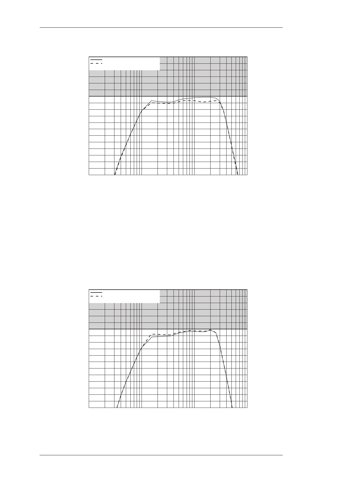
C4.6
T836/837 Functional Testing
M830-00
30/04/98 Copyright TEL
Figure 4.3 T836/837 Limiting Response
Wide Bandwidth
Narrow Bandwidth
100 500300 5k50
+10
+8
Modulation Level (dB ref. to max. dev.)
+6
+4
+2
+0
-2
-4
-6
-8
-10
-12
-14
-16
-18
-20
-22
10 20 30 200 1k 2k 3k 10k
Frequency (Hz)
Peak + max. dev. = +4.9kHz @ 1500Hz
Peak - max. dev. = -4.4kHz @ 2500Hz
Above limiting (steady-state)
Mid Bandwidth
The mid bandwidth graph is the same shape as the wide bandwidth graph. The devia-
tion figures are as follows:
peak + max. deviation = +4kHz
peak - max. deviation = -4kHz.
100 500300 5k50
+10
+8
Modulation Level (dB ref. to max. dev.)
+6
+4
+2
+0
-2
-4
-6
-8
-10
-12
-14
-16
-18
-20
-22
10 20 30 200 1k 2k 3k 10k
Frequency (Hz)
Peak + max. dev. = +2.4kHz @ 2000Hz
Peak - max. dev. = -2.5kHz @ 2000Hz
Above limiting (steady-state)

M830-00
T836/837 Functional Testing
C4.7
Copyright TEL 23/07/99
4.6 Audio Level Input Sensitivity
• Adjust RV210 (line sensitivity) fully clockwise.
• Check that the input sensitivities are better than those specified below:
Note:
A degraded signal to noise ratio can be expected with the compressor
selected. The extent of the degradation is dependent on the audio input
level.
Line Input 600 ohms, ±3kHz (±2.4kHz) [±1.5kHz] deviation at
1kHz:
with compressor -50dBm
without compressor -30dBm
Microphone Input 600 ohms, ±3kHz (±2.4kHz) [±1.5kHz] deviation at
1kHz:
with compressor -75dBm
without compressor -55dBm
CTCSS Input 1kHz deviation at 150Hz 500mV rms
Editor’s Note:
The CTCSS adjustment procedure described in Section 4.7 has been
moved to a more appropriate location in Section 3 as part of the Ini-
tial Tuning & Adjustment procedure (refer to Section 3.4.5 and Sec-
tion 3.9.3).

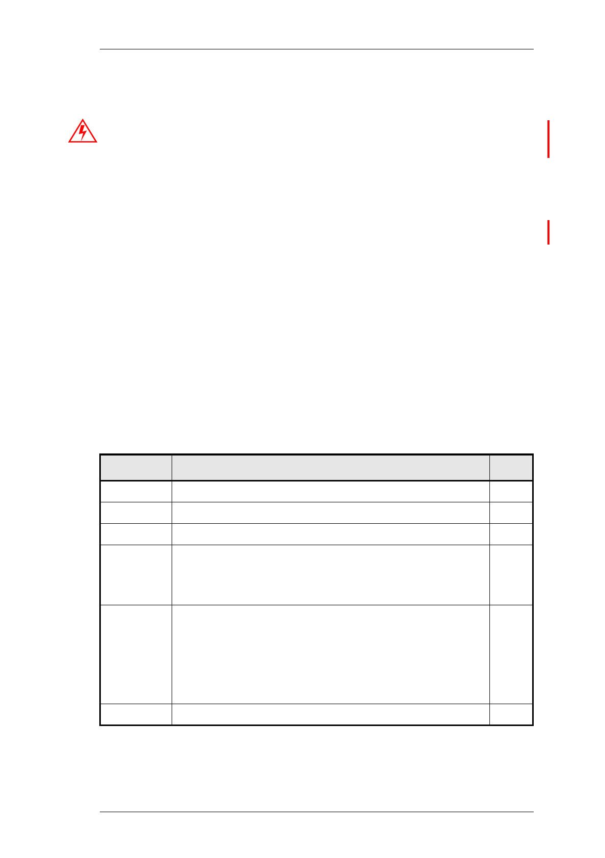
M830-00
T836/837 Fault Finding
C5.1
Copyright TEL 23/07/99
5 T836/837 Fault Finding
Caution:
This equipment contains CMOS devices which are susceptible to dam-
age from static charges. Refer to Section 1.2 in Part A for more infor-
mation on anti-static procedures when handling these devices.
The following test procedures and fault finding flow charts may be used to help locate a
hardware problem, however they are by no means a complete fault finding procedure.
If you still cannot trace the fault after progressing through them in a logical manner,
contact your nearest Tait Dealer or Customer Service Organisation. If necessary, you
can get additional technical help from Customer Support, Radio Systems Division, Tait
Electronics Ltd, Christchurch, New Zealand (full contact details are on page 2).
Note 1:
In this and following sections deviation settings are given first for wide
bandwidth sets, followed by settings in brackets for mid bandwidth sets ( )
and narrow bandwidth sets [ ].
Note 2:
Unless otherwise specified, the term "PGM800Win" used in this and follow-
ing sections refers to version 2.00 and later of the software.
Refer to Section 6 where the parts lists, grid reference index and diagrams will provide
detailed information on identifying and locating components and test points on the
main PCB. The parts list and diagrams for the VCO PCB are in Part E.
The following topics are covered in this section
Section Title Page
5.1 Visual Checks 5.3
5.2 Component Checks 5.3
5.3 Front Panel LED Indicator 5.3
5.4
5.4.1
5.4.2
DC Checks
Power Rails
VCO Locking
5.4
5.4
5.4
5.5
5.5.1
5.5.2
5.5.3
5.5.4
RF Checks
T836 Drive Power
T836 PA Output Power
T837 Output Power
Audio And Modulation
5.5
5.5
5.5
5.5
5.6
5.6 PGM800Win Generated Errors 5.7

C5.2
T836/837 Fault Finding
M830-00
30/04/98 Copyright TEL
5.7
5.7.1
5.7.1.1
5.7.1.2
5.7.1.3
5.7.2
5.7.3
5.7.4
5.7.5
5.7.6
5.7.7
Fault Finding Charts
Microcontroller
Basic Checks
Serial Communications
CTCSS Encode
Regulator
Synthesiser
T836 Drive Amplifier
T836 PA & Power Control
T837 Exciter Drive Amplifier
Audio Processor
5.8
5.8
5.8
5.9
5.10
5.11
5.12
5.15
5.16
5.17
5.18
5.8 To Replace The T836 PA Transistors (Q415 & Q425) 5.19
Figure Title Page
5.1
5.2
RF Diode Probe Circuit
Positioning Of Components Around Q425 & Q415
5.5
5.20
Section Title Page
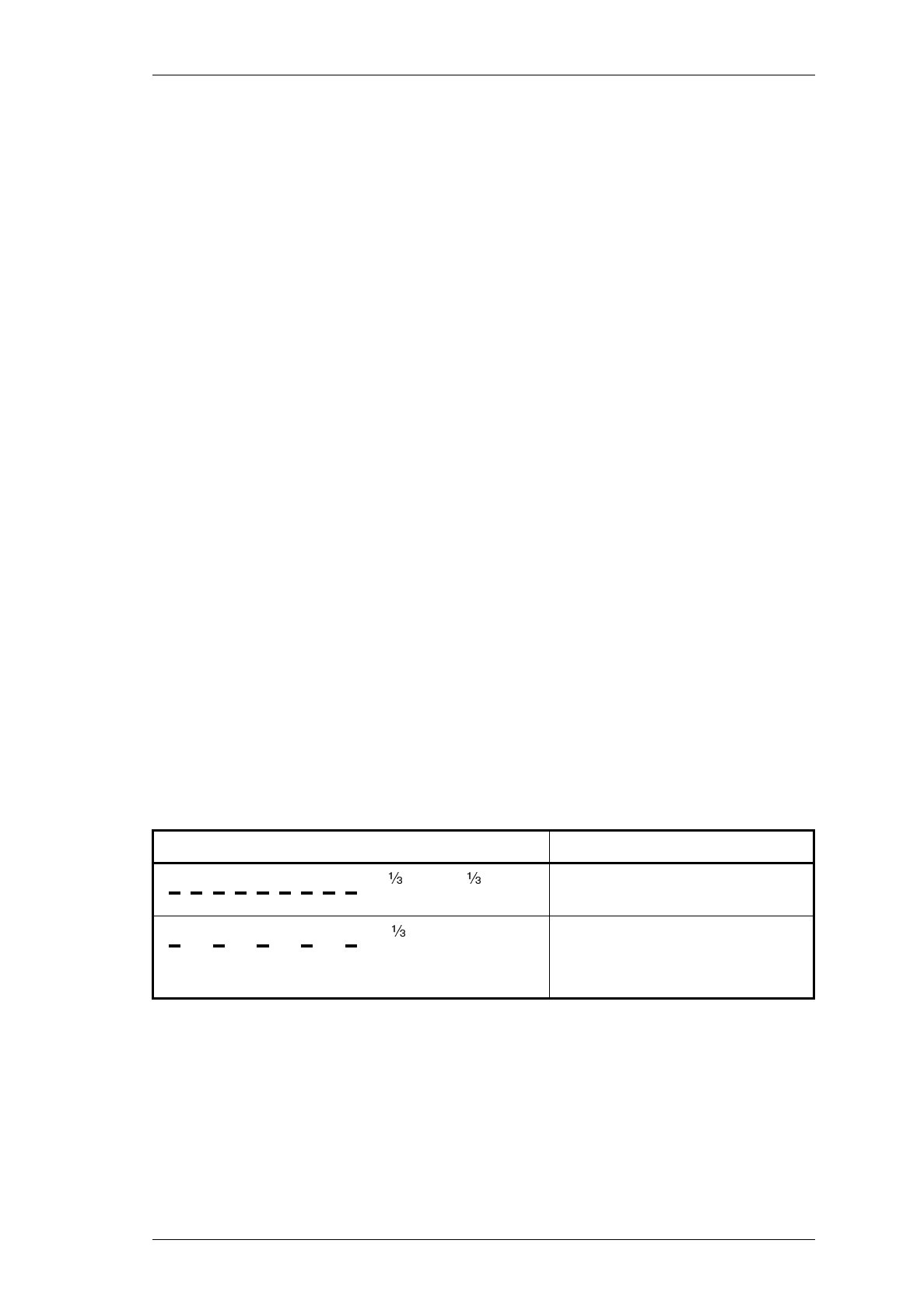
M830-00
T836/837 Fault Finding
C5.3
Copyright TEL 30/04/98
5.1 Visual Checks
Remove the covers from the T836/837 and inspect the PCB for damaged or broken com-
ponents, paying particular attention to the surface mounted devices (SMD's).
Check for defective solder joints. If repair or replacement is considered necessary, refer
to Section 3 of Part A.
5.2 Component Checks
If you suspect a transistor is faulty, you can assess its performance by measuring the for-
ward and reverse resistance of the junctions. Unless the device is completely desol-
dered, first make sure that the transistor is not shunted by some circuit resistance. Use a
good quality EVM (e.g. Fluke 75) for taking the measurements (or a 20k ohm/V or bet-
ter multimeter, using only the medium or low resistance ranges).
The collector current drawn by multi-junction transistors is a further guide to their per-
formance.
If an IC is suspect, the most reliable check is to measure the DC operating voltages. Due
to the catastrophic nature of most IC failures, the pin voltages will usually be markedly
different from the recommended values in the presence of a fault. The recommended
values can be obtained from either the circuit diagram or the component data catalogue.
5.3 Front Panel LED Indicator
The green "Supply" LED on the T836/837 front panel will flash according to the condi-
tions described in the following table:
Where two or more conditions occur at the same time, the precedence is in the order
shown above (i.e. T836/837 linked has the highest priority, followed by internal error).
Flash Rate Condition
fast ( sec. on/ sec. off
approx.) T836/837 is linked with
PGM800Win
unequal ( sec. on/1 sec. off
approx.) microcontroller has detected an
internal communications error -
refer to Section 5.7.1

C5.4
T836/837 Fault Finding
M830-00
30/04/98 Copyright TEL
5.4 DC Checks
5.4.1 Power Rails
Refer to the test points and options diagrams in Section 6 for test point locations, and to
the regulator fault finding chart (Section 5.7.2) for fault diagnosis.
Check the 13.8V (TP601) and 9V (TP602) supplies at their test points in the regula-
tor compartment with a DMM.
Check the 5V (TP604) and 20V (TP603) rails at their respective test points in the
regulator compartment.
Check that Tx-Reg. (TP305 in the exciter compartment) comes up to 8.8V when the
exciter is keyed.
Check the +5V digital regulator output (TP607 in the regulator compartment).
Check for short circuits.
5.4.2 VCO Locking
Key the exciter.
Using a DMM, monitor the VCO control voltage at PL4-1 or the junction of L1 and
R1 on the VCO PCB.
If the synthesiser is locked and the VCO aligned, the voltage at this point should
be between 5 and 13V.
If the VCO is not locked, refer to the synthesiser fault finding chart (Section 5.7.3).
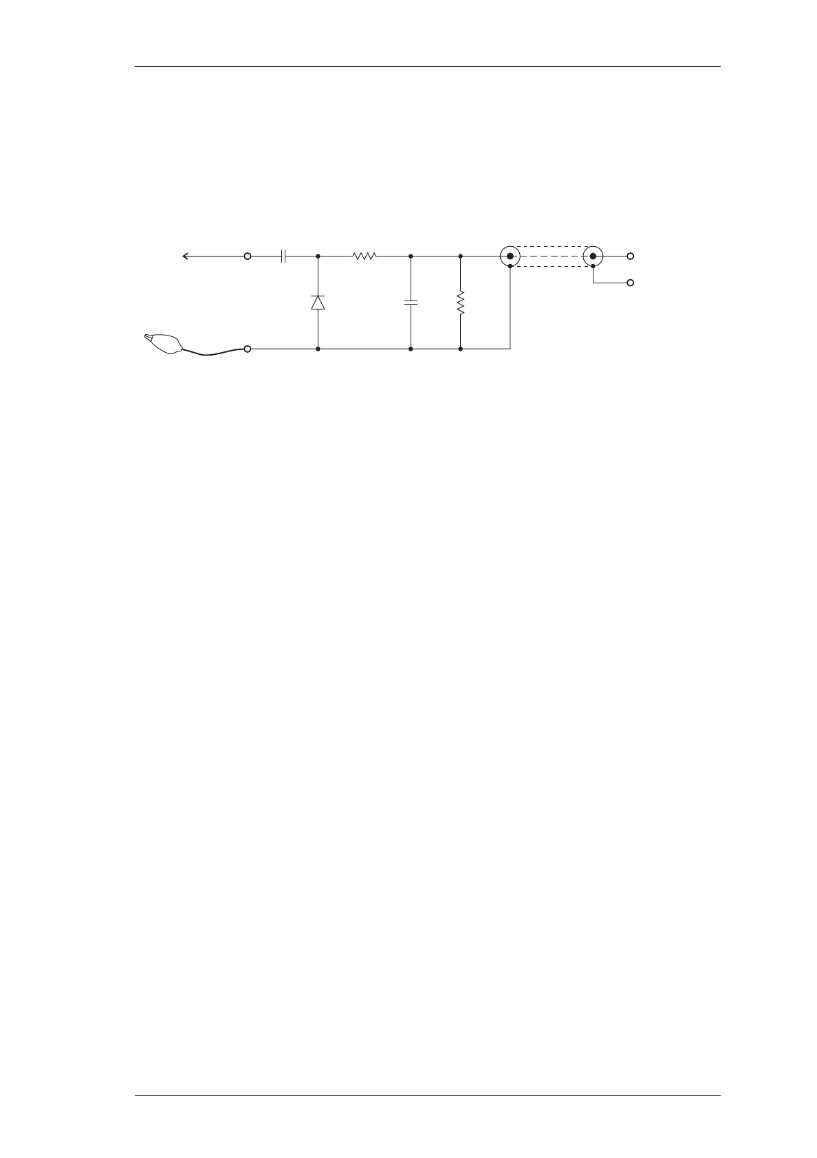
M830-00
T836/837 Fault Finding
C5.5
Copyright TEL 30/04/98
5.5 RF Checks
In-circuit RF levels may be measured with an RF probe on which the earth lead has been
shortened to a minimum (i.e. 13mm). Refer to the circuit diagrams for typical levels.
Figure 5.1 shows a suitable RF probe circuit.
Figure 5.1 RF Diode Probe Circuit
5.5.1 T836 Drive Power
Refer to the drive amplifier fault finding chart (Section 5.7.4).
Ensure that the VCO locks (refer to Section 5.4.2).
Connect the drive output to a power meter and key the transmitter.
Check that the output power is between 600 and 1000mW.
Note:
If the synthesiser is out of lock, the lock detector (synthesiser IC740 and
comparator IC750) will prevent the RF signal from reaching the PA by
switching the supply to the exciter amplifier (Q340, Q345).
5.5.2 T836 PA Output Power
Reconnect the drive output to the PA input.
Connect the PA to a power meter and key the transmitter.
Check that the output power is >30W with RV320 (power adjust) adjusted fully
clockwise.
5.5.3 T837 Output Power
Refer to the exciter drive amplifier fault finding chart (Section 5.7.6).
Ensure that the VCO locks (refer to Section 5.4.2).
100k
10k
1n
1n
1N6263
Coax
Probe
Earthing Clip
DC to DVM or
Oscilloscope
This unit is not suitable for use on high power RF circuits.

C5.6
T836/837 Fault Finding
M830-00
30/04/98 Copyright TEL
Connect the exciter output to a power meter and key the exciter.
Check that the output power is between 600 and 1000mW.
Note:
If the synthesiser is out of lock, the lock detector (synthesiser IC740 and
comparator IC750) will prevent the RF signal from reaching the PA by
switching the supply to the exciter amplifier (Q340, Q345).
5.5.4 Audio And Modulation
Refer to the audio processor fault finding chart (Section 5.7.7).
Set up the audio processor as described in Section 3.9.
Check that the demodulated RF output has the frequency response referred to in
Section 4.5 with at least ±5kHz (±4kHz) [±2.5kHz] deviation available at 1kHz
modulating frequency.
If the above result is not achieved, either the two modulators are incorrectly adjusted or
a fault condition exists.

M830-00
T836/837 Fault Finding
C5.7
Copyright TEL 30/04/98
5.6 PGM800Win Generated Errors
The following errors are those most likely to occur using PGM800Win. Refer to the
PGM800Win software user’s manual for a complete list of error messages.
Channel Switch Set
The programmed default channel change was not accepted by the base station because a
channel is selected externally. Try turning the external channel switch off to change the
default channel in PGM800Win.
Synth Out Of Lock
The synthesiser received incorrect data, or the data was corrupted. Enter a frequency
within the VCO switching range, or tune the VCO.
Internal Error
Data could not be read from the base station due to an internal error. Check for shorts
or open circuits on the SDA, SCK, SYNTH and EPOT lines. The SDA, SCK and SYNTH
are normally high, and the EPOT is normally low.
Write/Read To An Unlinked Module
The link to the module does not exist. Undefined error.
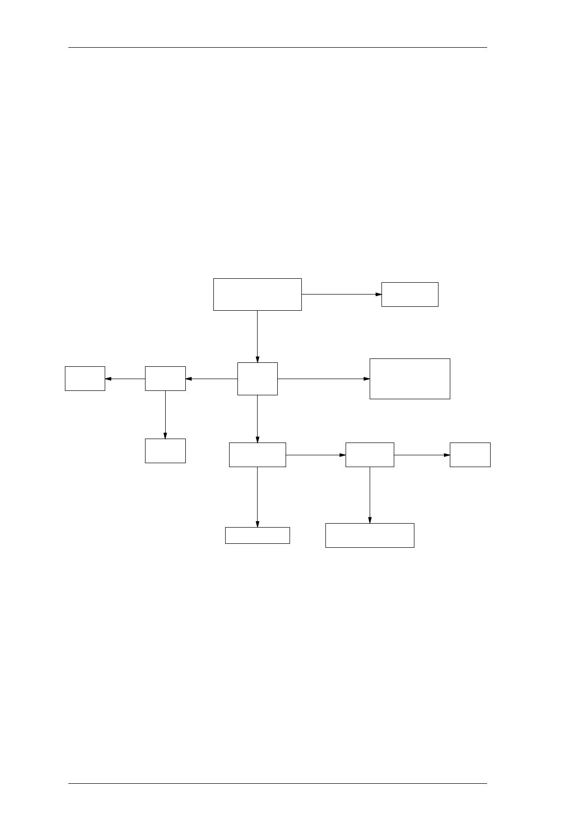
C5.8
T836/837 Fault Finding
M830-00
30/04/98 Copyright TEL
5.7 Fault Finding Charts
Note:
The standard test point designations used in this section are as follows:
TP601 13.8V
TP602 9V
TP603 20V
TP604 5V
5.7.1 Microcontroller (IC810)
5.7.1.1 Basic Checks
Pulsing Check state
of pin 35.
Y
Is pin 30
pulsing?
High or open circuit
Y
Static high/low
Check state of
pins 36 to 43.
Low/floating
High
Is the 12.8MHz clock
present on IC810 pin 21
(microcontroller)?
N
Replace
IC810.
Check IC740
(synthesiser).
*digital storage oscilloscope
Replace IC810.
Check the
state of
pin 10.
N Pulsing
Low
Replace
IC810.
Use a DSO* to check
operation of IC650
(i.e. active high
pulse at power up).
Replace
IC650.
Correct the fault causing
pin 35 to be low/floating.
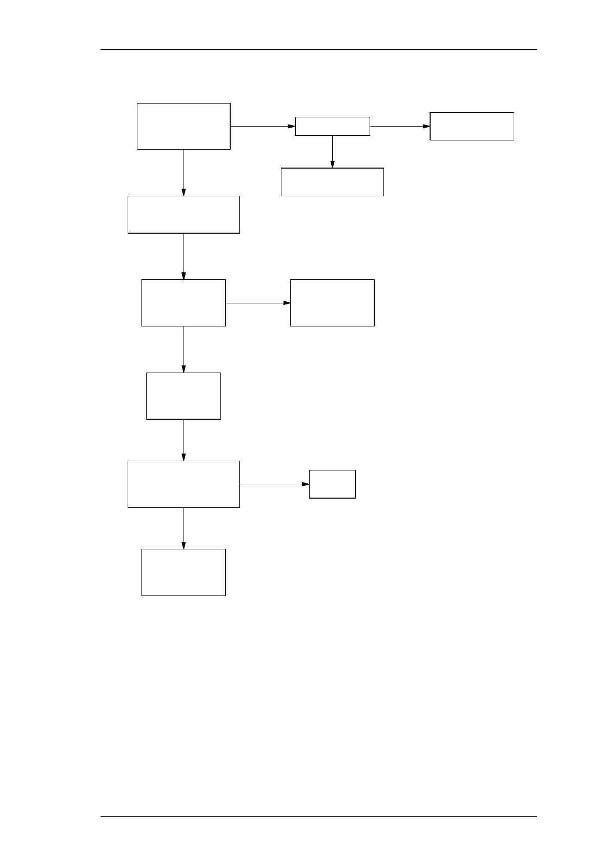
M830-00
T836/837 Fault Finding
C5.9
Copyright TEL 30/04/98
5.7.1.2 Serial Communication
Check pin state.
Y
Low/floatin
g
N
Noise
on pin
Disconnect the
pro
g
rammin
g
lead.
Is IC810 pin 11 hi
g
h?
(microcontroller)
Y*di
g
ital stora
g
e
oscilloscope
Use PGM800Win
to send a POLL
command to the
radio.
Check the transistor
interface circuitry
and/or replace the
pro
g
rammin
g
lead.
Check the SERIAL-COM
and AUDIO-1/2 links.
Replace
IC810.
Check the transistor
interface circuitry
and/or replace the
pro
g
rammin
g
lead.
Check the transistor
interface circuitry.
Check IC810 pin 13
with a DSO. Is there
a response from IC810 after
a poll command is sent?
N
Y
Connect the pro
g
rammin
g
lead and use PGM800Win
to read the rack/radio.
Check I/O pad P810
with a DSO*.
Does it swin
g
from
0 to 5V?
N
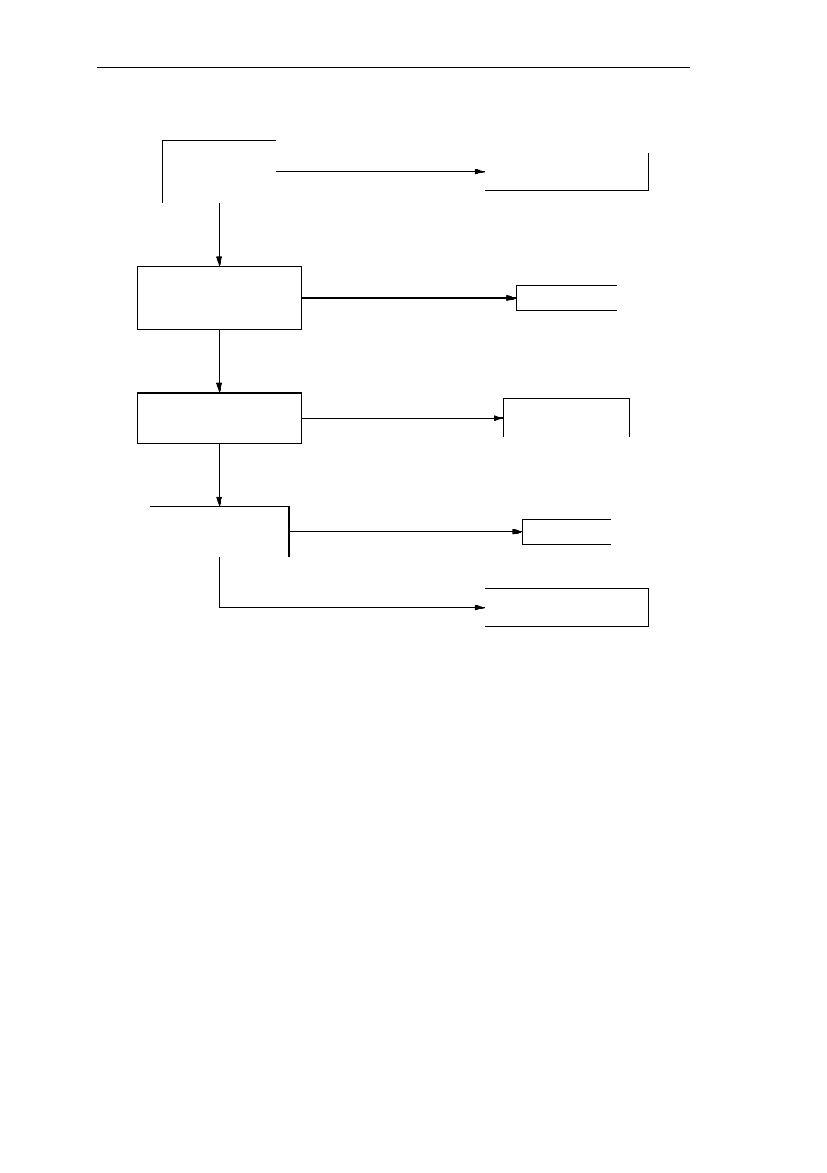
C5.10
T836/837 Fault Finding
M830-00
30/04/98 Copyright TEL
5.7.1.3 CTCSS Encode
Y
Y
Y
Replace IC810.
Use PGM800Win to
select a channel
with a CTCSS tone
pro
g
rammed.
Check serial communications.
(See separate flow chart).
Cannot select a channel
Check IC810 pins 24, 25
& 26 (microcontroller).
Are there 5V square waves at
the CTCSS frequency?
Check IC830 pins 1, 7 & 14.
Are there 9V square waves at
the CTCSS frequency?
Check IC830 pin 8.
Is there a sine wave
at the CTCSS frequency? Check RV805.
No tone
Check the filter circuit for bias
problems and/or short circuits.
Distorted tone
No square waves or
uneven mark/space ratio
No square waves or
uneven mark/space ratio Check IC830 circuitry
and repair/replace.
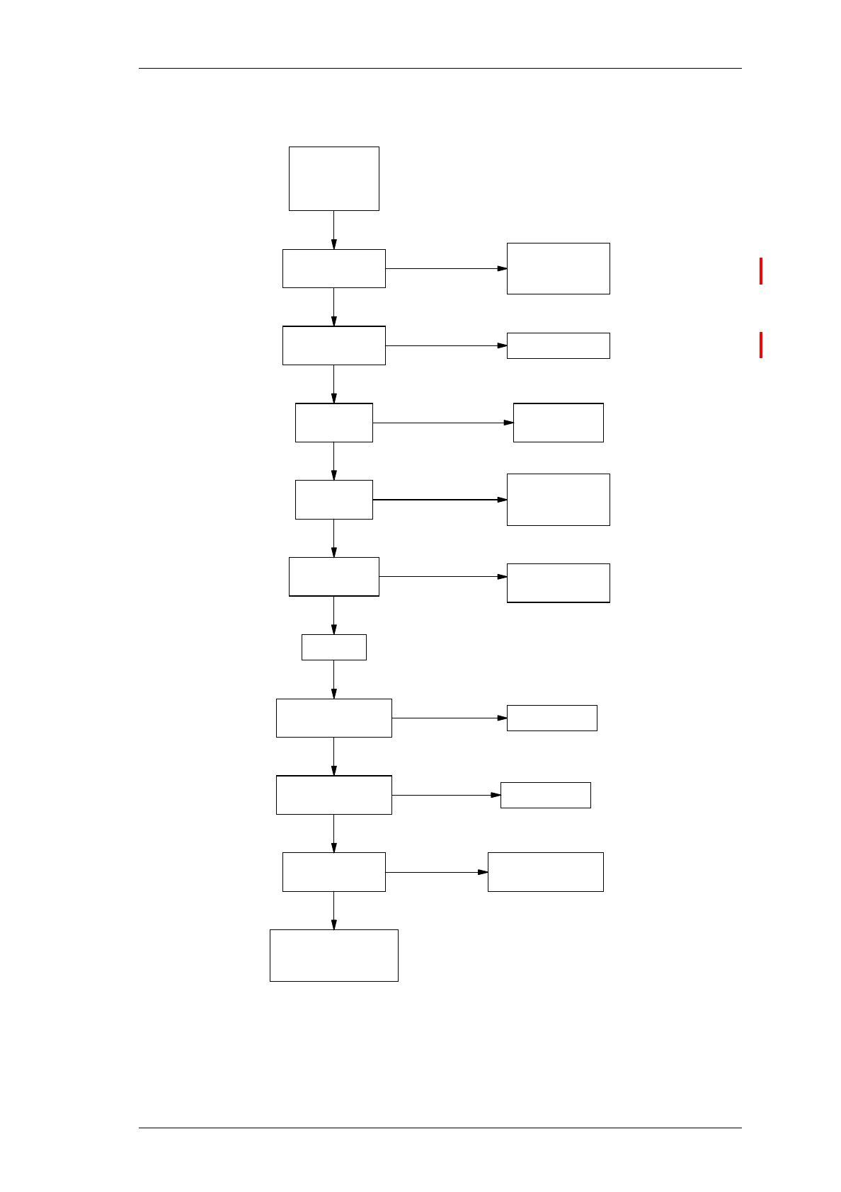
M830-00
T836/837 Fault Finding
C5.11
Copyright TEL 23/07/99
5.7.2 Regulator
N
Y
Check for
overheatin
g
components &
short circuits.
N
Y
Check Q630,
Q620 & IC640.
N
Y
9.0V present
on TP602?
Check Q660 is
switchin
g
at
approx. 150kHz.
N
Y
20V present
on TP603?
Check R615.
Replace IC610.
N
Y
+5V present on
IC610 pin 2?
Key Tx.
YRe
g
ulators OK.
N
8.8V present
on Tx re
g
. TP305?
Replace Q610.
Y
N
0V present
on Q860 collector?
Check Q860 and
associated circuitry.
Y
0.6V present on
Q860 base?
N
Re
g
ulators OK.
Check microcontroller
section.
Check continuity
from pin 9 of
D-ran
g
e 1.
13.8V present on
IC630 pin 3?
5.3V present on
IC630 pin 1? Replace IC630.
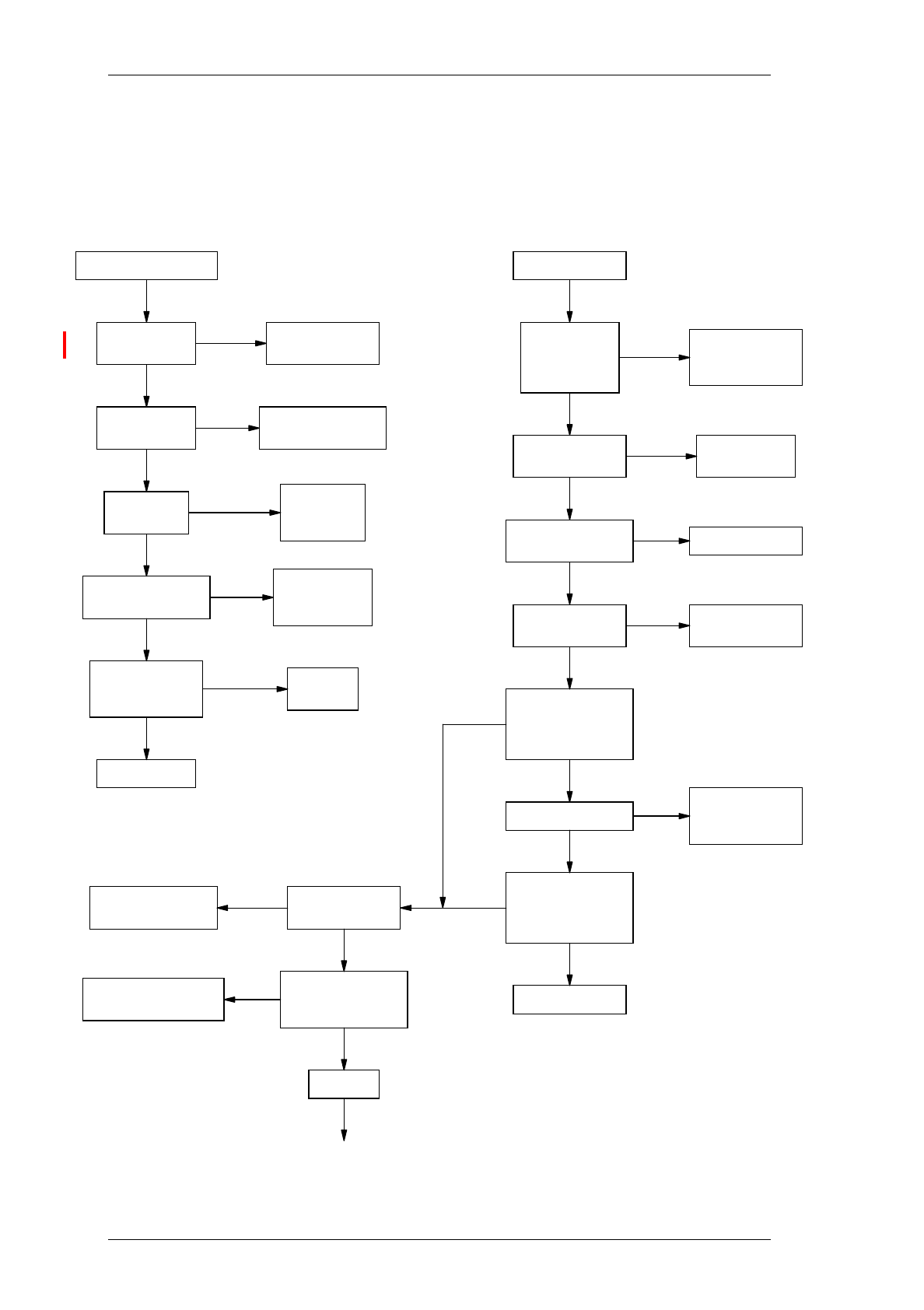
C5.12
T836/837 Fault Finding
M830-00
23/07/99 Copyright TEL
5.7.3 Synthesiser
Refer to the synthesiser circuit diagram (sheet 7) in Section 6 and the VCO circuit dia-
gram in Part E.
N
A B
Check biasin
g
resistors, Q4 & Q5.
N
Y
N
8.3V present
at VCO?
DC V present
at Q4 & Q5?
9V present at
VCO Q4/Q5?
No VCO RF output.
Y
DC V present at
VCO, Q1, Q2 & Q3?
Check biasin
g
resistors, Q1,
Q2 & Q3.
Y
N
Capacitors OK?
Check for cracks,
shorts, etc.
N
Y
Replace VCO.
Replace
if faulty.
Y
N
Y
N
N
N
Y
Y
DC V present
on Q795 emitter?
Check 9V supply.
9V present on
Q795 divider buffer?
20V inverter
supply faulty.
20V present
on IC750 pin 8?
Check 5V re
g
. &
supply resistor
to each IC.
+5V present at
IC700, IC710,
IC740, IC720
& IC730?
VCO out of lock.
Y
Y
Y
Continued on the next pa
g
e
Y
Does VCO trimmer
adjust for stable
control line
between 5 & 13V?
VCO freq. correct?
Does VCO trimmer
adjust for required
frequency ran
g
e
between 5 & 13V?
Synthesiser OK.
VCO trimmer
freq. ran
g
e OK?
Check VCO tunin
g
caps & trimmer.
Is 8MHz VCO ran
g
e
achieved between
5 & 13V?
VCO OK.
N
N
NN
N
Y
Y
Recheck
pro
g
rammin
g
via PGM800Win.
Check Q5 C
multiplier
(synth).
Check biasin
g
resistors & Q795.
Check #C5, #C3, #C4,
CV1 & D1-D4 in VCO.
Check Tx re
g
.,
Q610 & 9V re
g
.
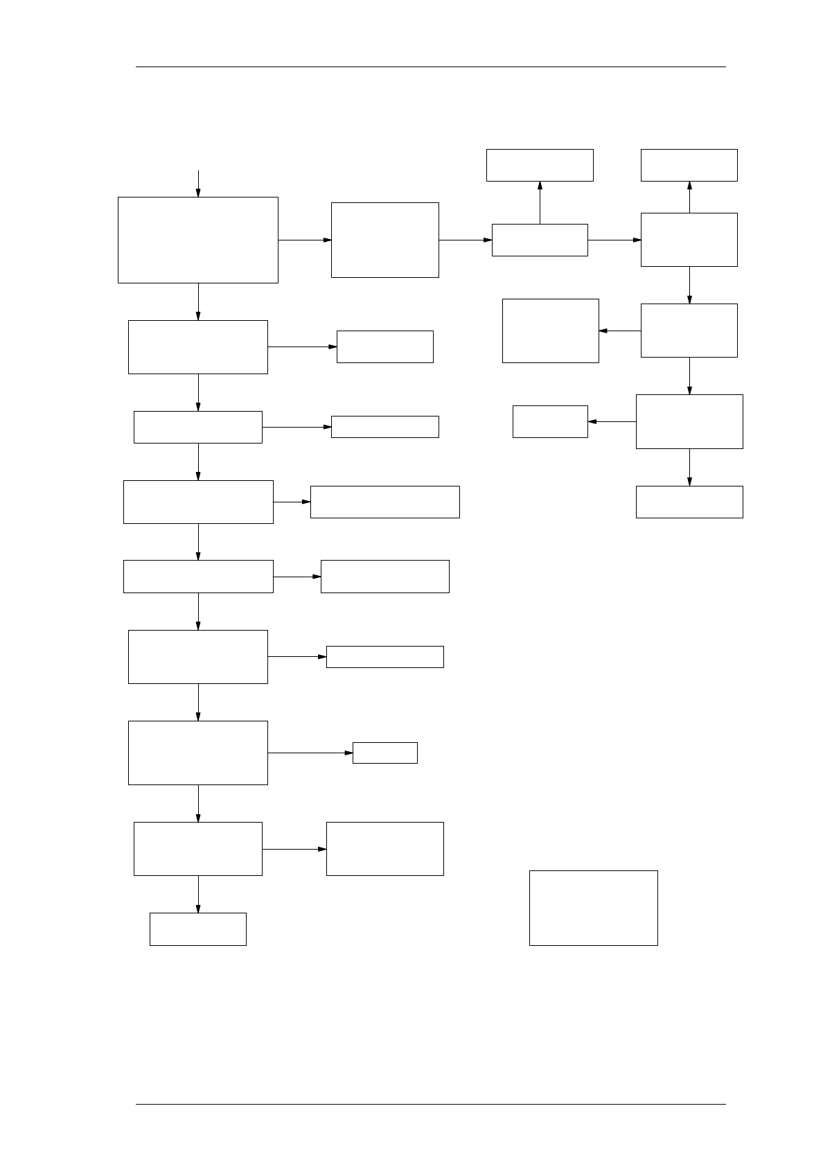
M830-00
T836/837 Fault Finding
C5.13
Copyright TEL 30/04/98
Programming and
serial bus OK?
Check programming.
Check serial bus
when programming
i.e. clock/data/enable
activity (IC740 pins
18, 19 & 17). N
Check loop filter components
R775, C774, C776, R510,
C505, IC750. Is the supply
to IC750 +20V +4, -2V?
Check regulator circuitry.
Check C772, R774, R772,
C770, R763 & Q790.
Check Q760, Q780,
R766 & C765.
Check charge pump components
(Q775 & Q780) and Q790.
Check R762 & C762.
Check the signal path from
the VCO to synthesiser.
Measure the frequency from
the VCO at IC740 pin 11 using
a frequency counter.
Is the level >-10dBm?
Does the frequency adjust
as the VCO trimmer is
adjusted (out of lock)?
Check VCO.
Y
Y
Y
Signal
Y
Y
Y
No signal
Replace synthesiser
(IC740).
Y
N Y
Y
N
N
N
N
Check phase detector output
pins (IC740 pins 3 & 4).
Are there very narrow pulses
(~50ns) at the reference frequency?
(i.e. 5kHz : 200µs period
6.25kHz : 160µs period)
*See Note below.
Is the charge pump bias
voltage at the base of
Q760 & Q780 between
3.5 and 5V? (5V when locked)
N
Is the voltage on C762,
R760, and R758 9V ±0.2V?
Is the loop filter reference
voltage at C772 (+) 6.5V ±0.2V?
N
Check divider buffer
circuit (Q795) and bias
voltages on Q795 emitter
(1.3V ±0.2V).
*Note:
When locked, both of these
are very narrow (~50ns).
If unlocked, one will be
very narrow (~50ns),
and the other wide (>15µs).
Replace synthesiser
(IC740).
Continued from previous page
B
Is the charge pump voltage
on Q790 gate between
3 and 8.5V? (6.5V ±0.2V locked)
Is reference
clock present
at IC740 pin 20
(200kHz >4.5Vpp)?
Check microcontroller
section (IC810).
N
Is reference
clock present
at IC730 pin 12
(200kHz >4.5Vpp)?
Is reference
clock present
at IC730 pin 1
(12.8MHz >4.0Vpp)?
Check TCXO (IC700)
and buffers (IC710).
N
N
Y
Y
Check phase
modulator sections:
IC720, Q710, Q720,
D710, Q730, Q740,
D720.
Check divider
IC730.
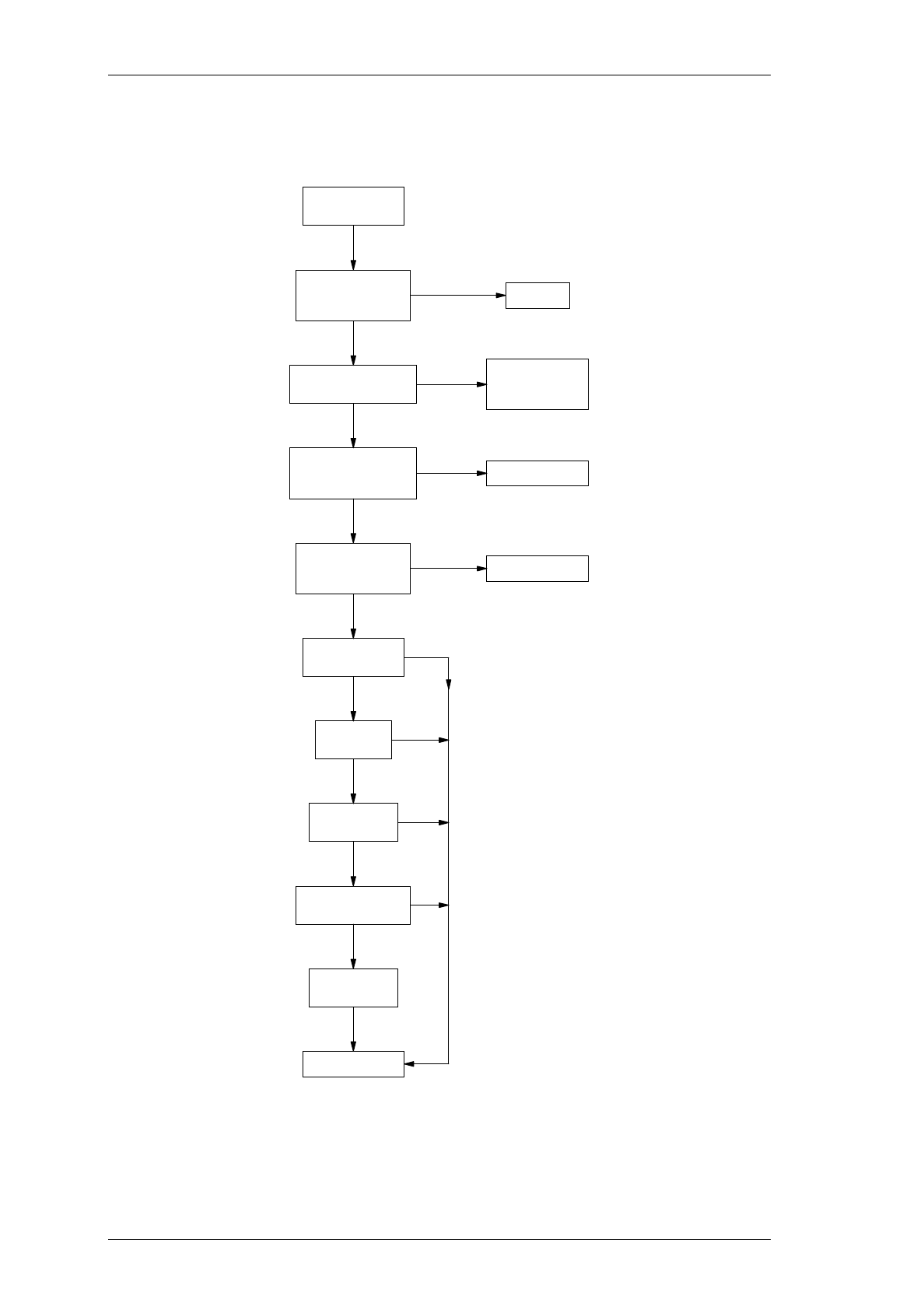
C5.14
T836/837 Fault Finding
M830-00
30/04/98 Copyright TEL
Y
N
Y
Y
VCO phase locked?
5-13V present on
control line?
Correct DC V
present on Q1 VCO?
N
Check inductors,
biasing resistors
& Q1.
Replace if faulty.
Go to B.
Loop filter &
components around
op. amp. (IC750) OK?
N
Noisy synth;
poor residual FM.
C
Isolate audio
modulation on VCO;
still noisy? Trace audio fault.
Y
Y
N
Y
Y
Y
Change trimmer;
still noisy?
Change Q1;
still noisy?
Change TCXO;
still noisy?
Change varactors;
still noisy?
Replace VCO
assembly.
Synthesiser OK.
N
N
N
N
Y
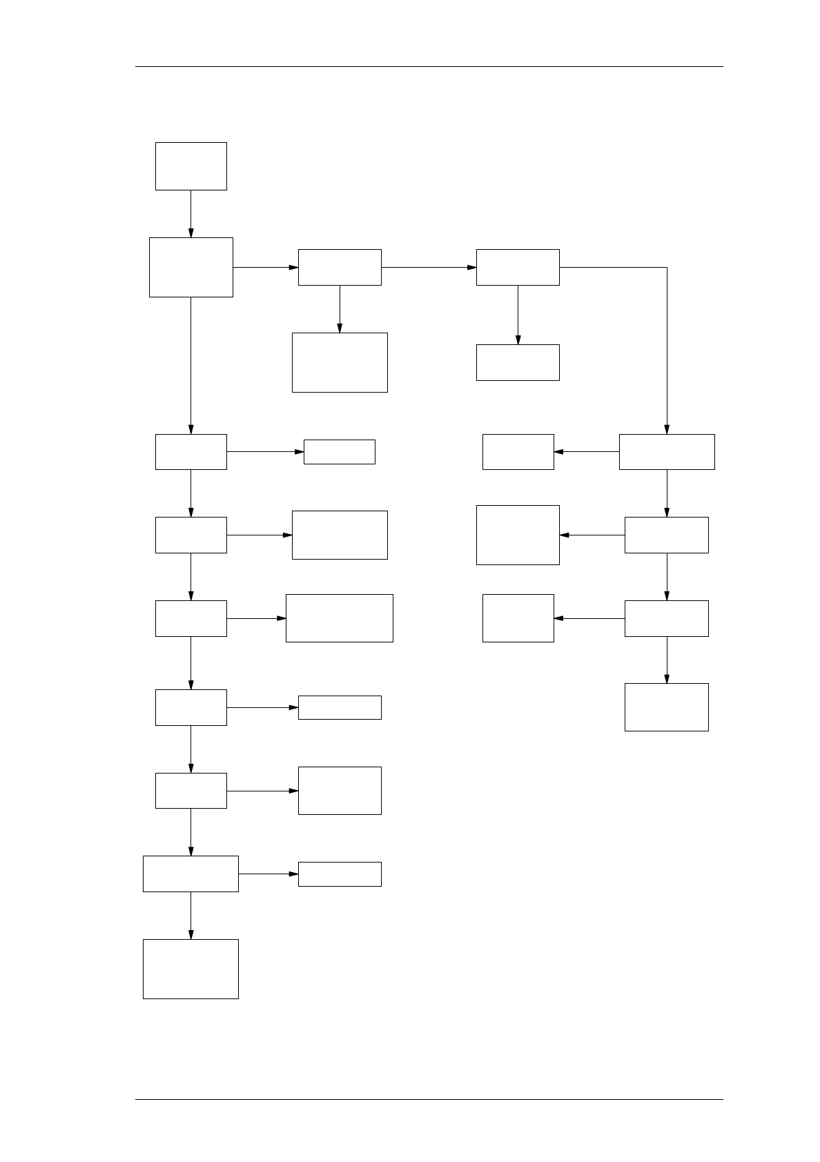
M830-00
T836/837 Fault Finding
C5.15
Copyright TEL 30/04/98
5.7.4 T836 Drive Amplifier
3.5V on Q365
collector?
10.5V on Q370
collector?
10.5V on Q315
collector?
Check continuity
of power rails
& DC paths to
Q365 & Q370.
>2.2V RF at
R359/R360?
>1.1V RF at
R360/R362?
Check attenuator
pad R359, R360,
R362.
>0.5V RF at
Q365 base?
Check C362, C365,
C368, Q365, D340,
D350, D360, L311.
>6V RF at
C379, L360? Check Q365.
>1.5V RF at
Q370 base.
Check signal
path between
Q365 & Q370.
>6V RF at
Q370 collector? Check Q370.
Check signal
path to output
incl. output
socket (SK310).
11V on IC330
pin 8?
Check Q310,
Q315 circuitry
& IC330.
Key exciter
& lock
synthesiser.
11V on IC330
pin 1?
NN N
YY
Y
Check VCO.
N
Y
N
Y
N
Y
N
Y
N
Y
N
Y
Check 9V &
13.8V supplies.
Check
regulators.
Check TP308
>+8V.
Check temp.
shutdown
circuit.
N
Y
N
Y
N
Y
Check lock det.
path back to
synth. IC740,
IC750, Q345.
Check TP314
<0.6V.
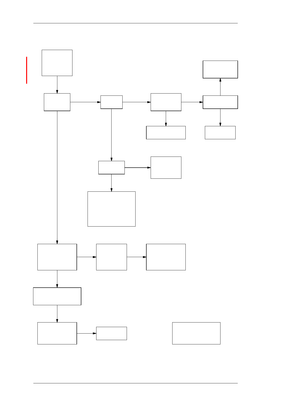
C5.16
T836/837 Fault Finding
M830-00
23/07/99 Copyright TEL
5.7.5 T836 PA & Power Control
10.5V
at L375?
Check Q415,
Q425 & circuitry,
LP filter.
Check +13.8V at
Q425 & Q415.
Check IC330,
Q310, Q315
& circuitry,
+13.8V supply.
Refer to Drive Amp.
Fault Findin
g
Chart. Check supply
circuitry.
Tx deliverin
g
full power
(>30W)?
Set RV320
(power adjust)
fully clockwise;
synth. locked;
key Tx.
<2.7V on
IC330 pin 2?
Check lock det. circuit;
TP308 should be >8V.
Check temp. shutdown
circuit (IC330);
TP314 should be <0.6V.
Check Q305, RV330.
Turn RV320 ccw.
Check power
drops to zero
slowly in a
controlled manner.
Does variation
of RV320
cause either
full power
or no power?
Check for break
in power sense
circuitry; directional
coupler D410,
D420 & circuitry.
Y
NY
NN
Y
N
Y
N
NY
Y
Check drive
at SK310
600-1000mW.
Y
Set RV320 so that
output power = 25W;
check L375 approx. 7V.
Momentarily remove
Tx load. Volta
g
e at
L375 decreases to
approx. 6.5V?
Power control
circuitry OK.
Note:
c/w = clockwise
cc/w = counterclockwise
or anticlockwise
Y
Normal operating conditions:
Forward power ≅1.6V
Reverse power ≅0.25V
IC330 pin 2 ≅2.7V
IC330 pin 3 ≅2.7V
IC330 pin 1 ≅9V
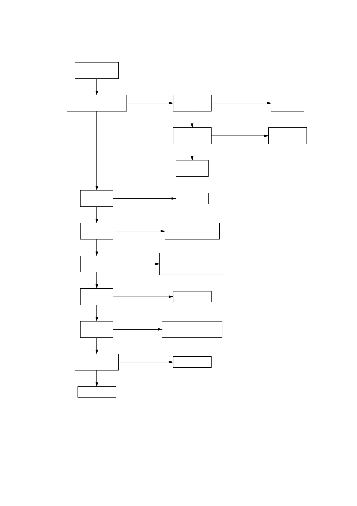
M830-00
T836/837 Fault Finding
C5.17
Copyright TEL 30/04/98
5.7.6 T837 Exciter Drive Amplifier
10.5V at Q315
collector?
Check IC330,
R324 & R326.
Check Q310
& Q315.
>2.2V RF at
R359/R360?
>1.1V RF at
R360/R362?
>0.5V RF at
Q365 base?
>6V RF at
C379, L360?
>1.5V RF at
Q370 base?
Check attenuator pad
R359, R360, R362.
Check Q365.
Check si
g
nal path
between Q365 & Q370.
Check Q370.
3.5V at Q365 collector?
10.5V at Q370 collector? Check
power rails.
>5V present on
IC330 pin 1?
Key exciter &
lock synthesiser.
Check VCO.
Check C362, C365, C368,
Q365, L311, D340, D350,
& D360.
>6V RF at
Q370 collector?
Drive amp. OK.
NY
YN
N
Y
N
Y
N
Y
N
Y
N
Y
N
Y
N
Y
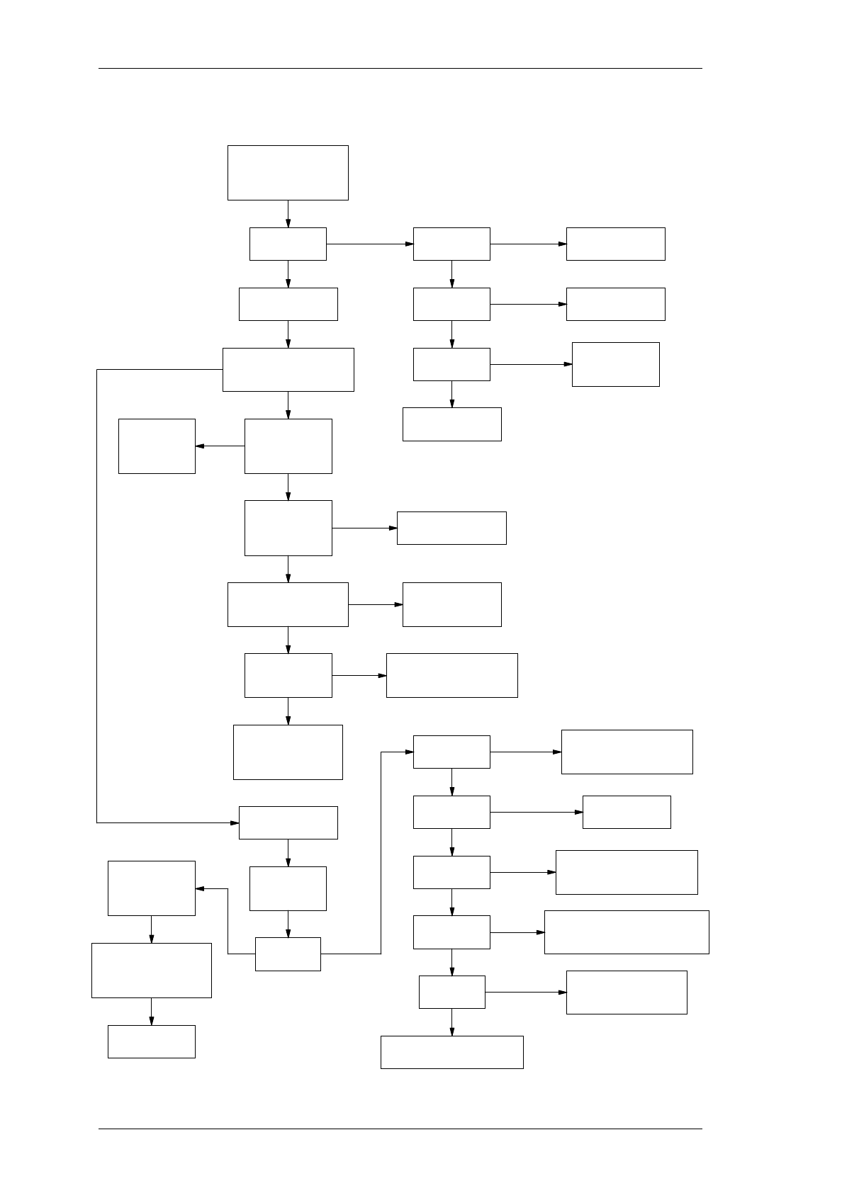
C5.18
T836/837 Fault Finding
M830-00
30/04/98 Copyright TEL
5.7.7 Audio Processor
N
IC240 pin 6
at 9V?
Key exciter &
lock synthesiser.
Connect 1kHz audio
to external CTCSS input.
Does exciter
modulate? Audio output at
IC260 pin 8?
NY
Check audio path to
VCO control line.
Check alignment
of modulators.
YN
Audio output at
IC260 pin 1?
YCheck buffer IC260
pins 8, 9 & 10.
N
Audio output at
IC260 pin 7?
Check low pass
filter stage IC260
pins 1, 2 & 3.
Y
Check stage IC260
pins 5, 6 & 7.
N
Demodulated audio
frequency response
flat between 50 & 300Hz?
Y
Check low
pass filter
stage IC260
pins 1, 2 & 3.
N
N
Y
Audio frequency
response IC260
pin 1 flat 300Hz
to 2kHz?
Audio frequency
response IC210
pin 8 6dB/octave
slope?
Check integrator
IC210 pins 8, 9, & 10.
N
Y
Audio superimposed
on 200kHz signal
IC720 pins 9 & 3 (synth)?
Check audio path
between integrator
& phase modulator.
N
Y
200kHz clipped
triangle wave at
IC720 pins 8 & 4?
Check IC720, Q710, Q720,
Q730, Q740, D710, D720,
C727, C729, C724 & C725
N
Y
Check loop filter
(IC750, pins 5, 6 & 7)
& associated
components.
Select standard
audio configuration.
Check pre-emphasis
network IC230 pins 12,
13 & 14 &/or low pass
filter IC260 pins 1, 2 & 3.
N
Y
Connect audio
to line input;
key exciter.
Does exciter
modulate?
YN
Demodulated
audio frequency
response as per
Section 4.5?
Audio processor
OK.
Audio signal at
IC210 pin 14?
Y
N
Audio signal at
IC230 pin 1?
N
Audio signal at
IC230 pin 14?
Y
N
Audio signal at
IC240 pin 4?
Y
N
Y
Check Q260 is not faulty or
being turned on inadvertently.
Y
Check audio path between
limiter IC210 pin 14 &
summing amp. IC260 pin 7.
Check IC210
pins 12, 13 & 14.
Check IC230 pins 1, 2 & 3 or
audio path between pre-
emphasis network & limiter.
Check IC230 pins 12, 13 & 14
or audio path between multiplexer
& pre-emphasis network.
Check IC240 or audio
path between line trans-
former & multiplexer.

M830-00
T836/837 Fault Finding
C5.19
Copyright TEL 23/07/99
5.8 To Replace The T836 PA Transistors
(Q415 & Q425)
Caution:
Failure to comply with the following procedure can result in failure of
the device due to poor heatsinking, or worse, can endanger the health
of the assembler if the beryllium oxide die carrier is smashed during
assembly.
Caution:
As the location of certain components in the PA is critical to perform-
ance, it is important that any components removed or disturbed are
refitted in exactly the same position.
Caution:
Before attempting to remove a transistor, note the position, type and
value of each capacitor and resistor so that it can be replaced in exactly
the same position (refer to Figure 5.2).
Caution:
Do not apply too much heat or pressure to the PCB pads and tracks as
you may damage them or lift them from the PCB, causing permanent
damage to the transmitter.
Remove the resistors and/or chip capacitors from around the transistor.
Desolder the transistor tabs by heating with a soldering iron and lifting away
from the PCB with a screwdriver or thin stainless steel spike. Unscrew the transis-
tor stud nut and remove the device.
Remove any excess solder from the PCB pads with solder wick.
Trim the tabs of the replacement transistor so that the device sits neatly on the
PCB pads provided.
Lightly tin the underside of the transistor tabs. Remove any excess solder to leave
a thin, even layer on the tabs.
Apply a small amount of heatsink compound (Dow-Corning 340 or equivalent) to
the transistor mounting surface. Sufficient compound should be used to ensure
an even film over the entire mounting surface.
Place the transistor on the PCB in the correct orientation and ensure the tabs are
flush to the surface. Lightly solder one tab to the PCB. Torque down the retaining
nut to the correct torque (0.7Nm/6in.lbf.).
Caution:
Do not solder all the tabs before torquing down otherwise the device
may be broken.
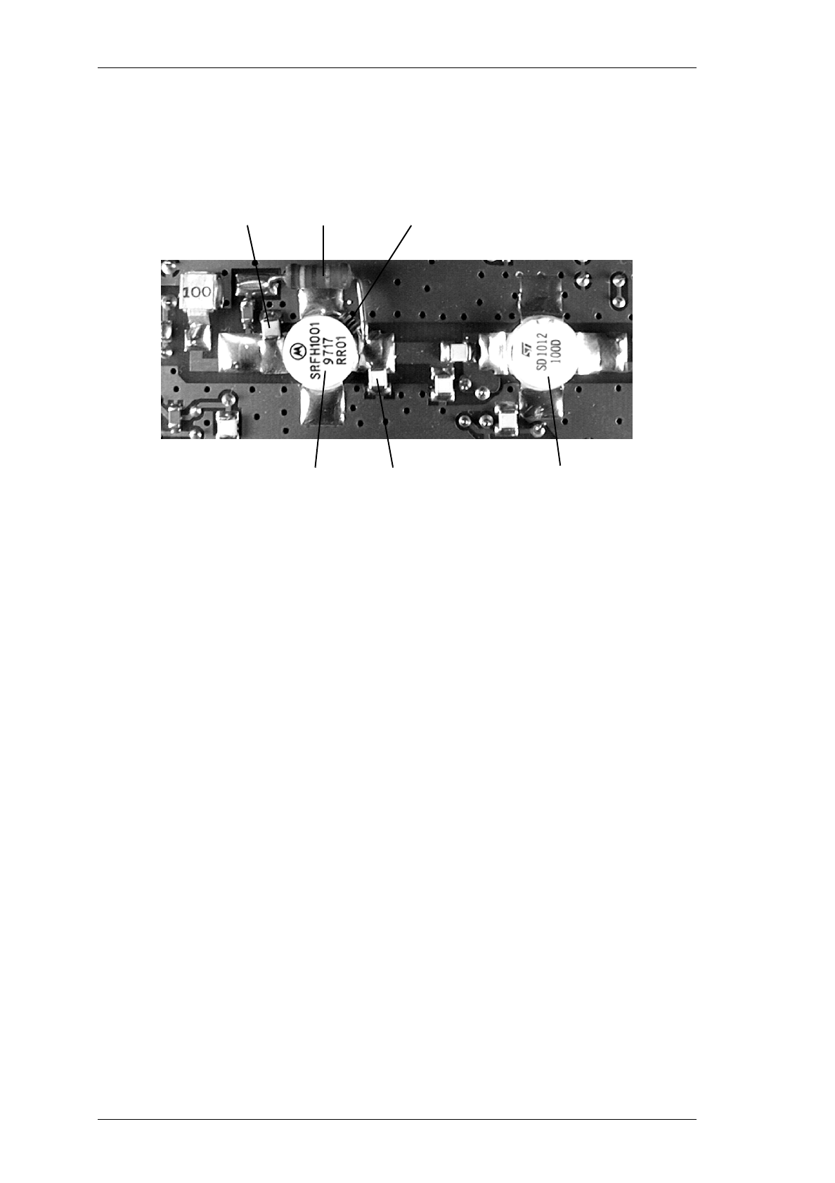
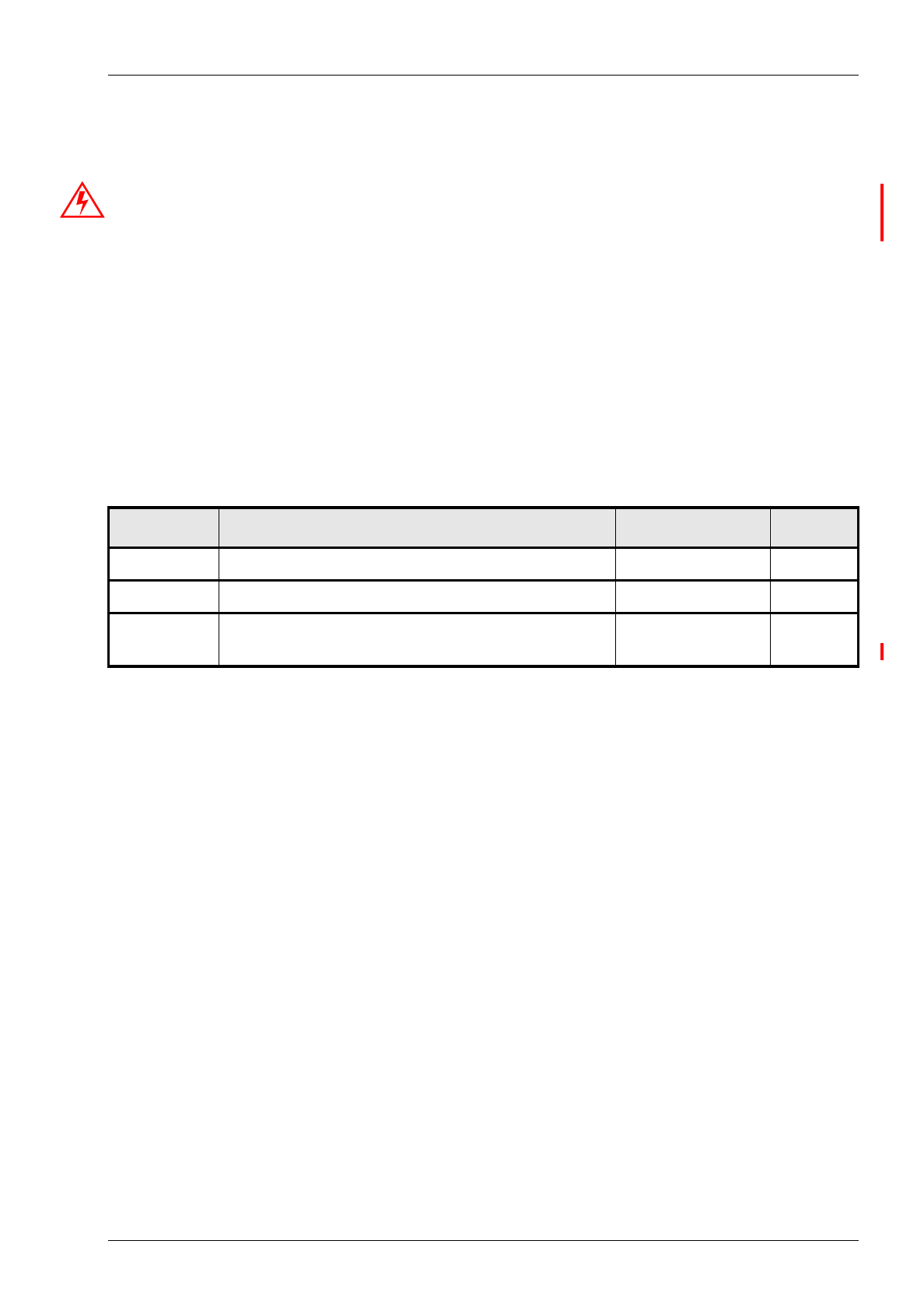
M830-00
T836/837 PCB Information
C6.1.1
Copyright TEL 23/07/99
6 T836/837 PCB Information
Caution:
This equipment contains CMOS devices which are susceptible to damage from
static charges. Refer to Section 1.2 in Part A for more information on anti-static
procedures when handling these devices.
This section provides the following information on the T836 transmitter and T837 exciter:
•parts lists
• grid reference indexes
• mechanical assembly drawings
•PCB layouts
• test points & options connections drawings
• circuit diagrams.
Section Title IPN Page
6.1 Introduction 6.1.3
6.2 T836 Transmitter PCB 220-01395-02 6.2.1
6.3 T837 Exciter PCB 220-01390-02
220-01390-03
6.3.1
6.3.27


M830-00
T836/837 PCB Information
C6.1.3
Copyright TEL 30/04/98
6.1 Introduction
Product Type Identification
You can identify the transmitter or exciter type by checking the product code printed on a label on
the rear of the chassis (product codes are explained in Section 1.3 in this Part of the manual, and Fig-
ure 1.1 in Part A shows typical labels). You can further verify the product type by checking the
placement of an SMD resistor in the table that is screen printed onto the top side of the PCB, similar
to the example drawn below (this table also appears in the resist layer on the bottom side of the
PCB). In this example, the resistor indicates that the product was built as a T836-10-XXXX.
Note:
The only function of this resistor is to indicate the product type. It has no effect on the
circuitry or operation of the transmitter or exciter.
PCB Identification
All PCBs are identified by a unique 10 digit “internal part number” (IPN), e.g. 220-12345-00, which
is screen printed onto the PCB (usually on the top side), as shown in the example below:
The last 2 digits of this number define the issue status, which starts at 00 and increments through 01,
02, 03, etc. as the PCB is updated. Some issue PCBs never reach full production status and are there-
fore not included in this manual. A letter following the 10 digit IPN has no relevance in identifying
the PCB for service purposes.
Note:
It is important that you identify which issue PCB you are working on so that you can
refer to the appropriate set of PCB information.
836- PRODUCT TYPE
836- 836-10 836-20
836- 836-13 836-23
PRODUCT TYPE 836-15 836-25

C6.1.4
T836/837 PCB Information
M830-00
30/04/98 Copyright TEL
Parts Lists
The 10 digit numbers (000-00000-00) in this Parts List are “internal part numbers” (IPNs). We can
process your spare parts orders more efficiently and accurately if you quote the IPN and provide a
brief description of the part.
The components listed in this parts list are divided into two main types: those with a circuit refer-
ence (e.g. C2, D1, R121, etc.) and those without (miscellaneous and mechanical).
Those with a circuit reference are grouped in alphabetical order and then in numerical order within
each group. Each component entry comprises three or four columns, as shown below:
The mechanical and miscellaneous section lists the variant and common parts in IPN order.
Parts List Amendments
At the front of the parts list is the Parts List Amendments box (an example of which is shown
below). This box contains a list of component changes which took place after the parts list and dia-
grams in this section were compiled. These changes (e.g. value changes, added/deleted compo-
nents, etc.) are listed by circuit reference in alphanumeric order and supersede the information
given in the parts list or diagrams. Components without circuit references are listed in IPN order.
The number in brackets at the end of each entry refers to the Tait internal Change Order document.
circuit reference -
lists components
in alphanumeric
order
variant column -
indicates that this is
a variant component
which is fitted only to
the product type listed
Internal Part Number -
order the component
b
y
this number
description -
gives a brief description
of the component
Parts List Amendments
R306 Changed from 180Ωto 560Ω(036-13560-00) to increase sensitivity (71003).
circuit reference
or IPN description
of change
IPN of new
component Change Order
number

M830-00
T836/837 PCB Information
C6.1.5
Copyright TEL 30/04/98
Variant Components
A variant component is one that has the same circuit reference but different value or specification in
different product types. Where two products share the same PCB, the term “variant” is also used to
describe components unplaced in one product. Variant components have a character prefix, such as
“&”, “=” or “#”, before the circuit reference (e.g. &R100).
The table below explains the variant prefixes used in T800 Series II products:
Grid Reference Index
This section contains a component grid reference index to help you find components and labelled
pads on the PCB layouts and circuit diagrams. This index lists the components and pads in alpha-
numeric order, along with the appropriate alphanumeric grid references, as shown below:
If the variant prefix is. . . the component will. . .
& change according to channel spacing
= change according to frequency stability
# change according to frequency range
% be placed or unplaced for special applications
*be unplaced in one product
(where two products share the same PCB)
circuit diagram
reference
PCB layout
reference
components listed
in alphanumeric order
layer number -
1 = top side layer
2 = bottom side layer
component location
on the layer
sheet number
component location
on the sheet

C6.1.6
T836/837 PCB Information
M830-00
30/04/98 Copyright TEL
Using CAD Circuit Diagrams
Reading a CAD circuit diagram is similar to reading a road map, in that both have an alphanumeric
border. The circuit diagrams in this manual use letters to represent the horizontal axis, and num-
bers for the vertical axis. These circuit diagram “grid references” are useful in following a circuit
that is spread over two or more sheets.
When a line representing part of the circuitry is discontinued, a reference will be given at the end of
the line to indicate where the rest of the circuitry is located, as shown below. The first digit refers to
the sheet number and the last two characters refer to the location on that sheet of the continuation of
the circuit (e.g. 1R3).
C301
4N7
R303
12
D
S
G
L310
33U
IF-SIG
4R4
C369
100P
C371
10U
R339
100K
%R338
100
DISCRIMINATOR
1R3
2R9
2R9
8A2
t
hese grid references
s
how where the circuit
is continued

M830-00
T836 PCB Information
C6.2.1
Copyright TEL 30/04/98
6.2 T836 Transmitter PCB
This section contains the following information.
IPN Section Page
220-011395-02 Parts List
Mechanical & Miscellaneous Parts
Mechanical Assembly
Grid Reference Index
PCB Layout - Top Side
PCB Layout - Bottom Side
Test Points & Options Connections - Top & Bottom Side
Transmitter Overview Diagram
Audio Processor Circuit Diagram
Exciter Circuit Diagram
PA Circuit Diagram
VCO Section Circuit Diagram
Regulators Circuit Diagram
Synthesiser Circuit Diagram
Microcontroller Circuit Diagram
Harmonic Filter Circuit Diagram
6.2.3
6.2.8
6.2.9
6.2.11
6.2.15
6.2.16
6.2.17
6.2.18
6.2.19
6.2.20
6.2.21
6.2.22
6.2.23
6.2.24
6.2.25
6.2.26


IPN 220-01395-02
M830-00
T836 PCB Information
C6.2.3
Copyright TEL 23/07/99
T836 Parts List (IPN 220-01395-02)
How To Use This Parts List
The components listed in this parts list are divided into two main types: those with a circuit reference (e.g. C2, D1, R121, etc.) and
those without (miscellaneous and mechanical).
Those with a circuit reference are grouped in alphabetical order and then in numerical order within each group. Each component
entry comprises three or four columns: the circuit reference, variant (if applicable), IPN and description. A number in the variant col-
umn indicates that this is a variant component which is fitted only to the product type listed. Static sensitive devices are indicated by
an (S) at the start of the description column.
The miscellaneous and mechanical section lists the variant and common parts in IPN order. Where possible, a number in the legend
column indicates their position in the mechanical assembly drawing.
The Parts List Amendments box below lists component changes that took place after the parts list and diagrams in this section were
compiled. These changes (e.g. value changes, added/deleted components, etc.) are listed by circuit reference in alphanumeric order
and supersede the information given in the parts list or diagrams. Components without circuit references are listed in IPN order.
Parts List Amendments
&C269 T836-16-0000/836-26-0000: changed from 1p5 (IPN 015-21150-01) to 4p7 (IPN 015-21470-01) for FCC Type
Approval requirements (710655).
C289 T836-16-0000/836-26-0000: changed from 47n (IPN 015-25470-08) to 68n (IPN 015-25680-08) for FCC Type
Approval requirements (710655).
C314 Deleted to improve low frequency stability (710137).
C316, C347 Changed from 22n (015-25220-08) to 47n (015-25470-08) to improve cyclic keying & standby current (710059).
#C448 136-156MHz (-10, -13 & -15): changed from 39p (015-02390-02) to 33p (015-02330-02) to improve low band per-
formance.
C910A, C950A 2p2 capacitors (015-01220-06) added on top of C910 & C950 to improve the low pass filter at 174MHz (710155).
D111 Changed from MR750 (IPN 001-00011-60) to MR2520L (IPN 001-00012-90) to provide overvoltage transient sup-
pression (750087/88/89/90/91/92).
IC710 Changed from 74HCV04 (IPN 002-74910-04) to 74HC04 (IPN 002-74900-04) to increase the gain of the TCXO
buffer (710312).
R313 Changed from 27k (036-15270-00) to 18k (036-15180-00) to improve cyclic keying & standby current (710059).
R320, R321 Changed from 47k (036-15470-00) to 33k (036-15330-00) to improve cyclic keying & standby current (710059).
Changed from 33k (036-15330-00) to 56k (036-15560-00) for ACP IETS 300-113 compliance (710158).
R355 Changed from 82k (036-15820-00) to 47k (036-15470-00) to improve cyclic keying & standby current (710059).
R356 Changed from 47k (036-15470-00) to 220k (036-16220-00) to improve cyclic keying & standby current (710059).
R357 Changed from 47k (036-15470-00) to 22k (036-15220-00) to improve cyclic keying & standby current (710059).
Changed from 22k (036-15220-00) to 47k (036-15470-00) for ACP IETS 300-113 compliance (710158).
R713 Changed from 22Ω (IPN 036-12220-00) to 0Ω (IPN 036-10000-00) to improve hum & noise performance (710837/
839/840/841).
RV220 Changed to IPN 042-05470-07 (47k preset) because IPN 042-05470-06 no longer available (710793/96/97/98).
303-11169-03 T800 chassis: replaced by 303-11169-04
312-01052-01 T800 top lid: replaced by 312-01052-02
312-01053-01 T800 bottom lid: replaced by 312-01053-02
349-00020-36 The two M3x8 Torx screws which secure the module into the rack frame have been replaced by M3x8 Pozidriv
screws (IPN 349-00020-55) (750101/2/3/5/6).
New chassis and lid tooling introduced, incorporating
mechanical improvements and better RF shielding
(750027, 750028 & 750029). Note that the new lids
should be used only with the new chassis.

IPN 220-01395-02
C6.2.4
T836 PCB Information
M830-00
30/04/98 Copyright TEL
Ref Var IPN Description Ref Var IPN Description
C201 020-07470-92 CAP BI-P RA 4M7 50V 6X11 5 LS
C202 020-07470-92 CAP BI-P RA 4M7 50V 6X11 5 LS
C204 020-07470-92 CAP BI-P RA 4M7 50V 6X11 5 LS
C205 020-07470-92 CAP BI-P RA 4M7 50V 6X11 5 LS
C207 014-07470-00 CAP TANT CHIP 4U7 3.5 X 2.8MM
C209 015-25470-08 CAP CER 0805 47N 10% X7R 50V
C210 015-06100-08 CAP CER 1206 100N 10% X7R 50V
C211 015-06100-08 CAP CER 1206 100N 10% X7R 50V
C213 025-08100-02 CAP TANT BEAD 10M 10% 16V
C215 014-08220-01 (L)CAP TANT 22UF10V276MSER
C217 015-24220-08 CAP CER 0805 2N2 10% X7R 50V
C219 015-24100-08 CAP CER 0805 1N 10% X7R 50V
C221 014-08220-01 (L)CAP TANT 22UF10V276MSER
C223 015-06100-08 CAP CER 1206 100N 10% X7R 50V
C225 015-06100-08 CAP CER 1206 100N 10% X7R 50V
C227 015-06100-08 CAP CER 1206 100N 10% X7R 50V
C229 015-23150-01 CAP CER 0805 150P 5% NPO 50V
C230 015-06100-08 CAP CER 1206 100N 10% X7R 50V
C232 015-23150-01 CAP CER 0805 150P 5% NPO 50V
C233 020-08470-02 CAP ELE RA 47M 16V 6X11MM
C235 015-24100-08 CAP CER 0805 1N 10% X7R 50V
C237 020-07100-02 CAP ELE RA 1M 50V 5X11MM
C239 020-07470-92 CAP BI-P RA 4M7 50V 6X11 5 LS
C241 015-06100-08 CAP CER 1206 100N 10% X7R 50V
C242 025-08100-02 CAP TANT BEAD 10M 10% 16V
C243 015-24100-08 CAP CER 0805 1N 10% X7R 50V
C245 015-23150-01 CAP CER 0805 150P 5% NPO 50V
C247 015-23150-01 CAP CER 0805 150P 5% NPO 50V
C249 015-24100-08 CAP CER 0805 1N 10% X7R 50V
C251 015-24100-08 CAP CER 0805 1N 10% X7R 50V
C253 015-24100-08 CAP CER 0805 1N 10% X7R 50V
C255 015-24100-08 CAP CER 0805 1N 10% X7R 50V
C257 015-22470-01 CAP CER 0805 47P 5% NPO 50V
C259 015-25470-08 CAP CER 0805 47N 10% X7R 50V
C260 015-06100-08 CAP CER 1206 100N 10% X7R 50V
C261 014-07470-00 CAP TANT CHIP 4U7 3.5 X 2.8MM
C263 020-09100-04 CAP ELE RA 100M 10V 6.3X9MM
C265 020-07470-92 CAP BI-P RA 4M7 50V 6X11 5 LS
C267 015-24470-08 CAP CER 0805 4N7 10% X7R 50V
&C269 10 015-21150-01 CAP CER 0805 1P5+-1/4P NPO 50V
&C269 13 015-21150-01 CAP CER 0805 1P5+-1/4P NPO 50V
&C269 15 015-21470-01 CAP CER 0805 4P7+-1/4P NPO 50V
&C269 20 015-21150-01 CAP CER 0805 1P5+-1/4P NPO 50V
&C269 23 015-21150-01 CAP CER 0805 1P5+-1/4P NPO 50V
&C269 25 015-21470-01 CAP CER 0805 4P7+-1/4P NPO 50V
C271 015-22470-01 CAP CER 0805 47P 5% NPO 50V
C273 015-25470-08 CAP CER 0805 47N 10% X7R 50V
C275 015-23120-01 CAP CER 0805 120P 5% NPO 50V
C277 015-25100-08 CAP CER 0805 10N 10% X7R 50V
C279 015-24100-08 CAP CER 0805 1N 10% X7R 50V
C281 015-25220-08 CAP CER 0805 22N 10% X7R 50V
C283 015-21470-01 CAP CER 0805 4P7+-1/4P NPO 50V
C285 015-21470-01 CAP CER 0805 4P7+-1/4P NPO 50V
C287 020-09100-04 CAP ELE RA 100M 10V 6.3X9MM
C289 015-25470-08 CAP CER 0805 47N 10% X7R 50V
C291 014-08220-01 (L)CAP TANT 22UF10V276MSER
C293 015-27100-10 CAP CER 0805 1M+80-20% Y5V 16V
%C294 015-22470-01 CAP CER 0805 47P 5% NPO 50V
%C295 022-06470-02 CAP MYLAR 470N 10% 50V
C302 025-08100-02 CAP TANT BEAD 10M 10% 16V
C308 015-24100-08 CAP CER 0805 1N 10% X7R 50V
C310 015-24100-08 CAP CER 0805 1N 10% X7R 50V
C312 015-24100-08 CAP CER 0805 1N 10% X7R 50V
C313 015-06100-08 CAP CER 1206 100N 10% X7R 50V
C316 015-25470-08 CAP CER 0805 47N 10% X7R 50V
C317 015-23100-01 CAP CER 0805 100P 5% NPO 50V
C318 015-24100-08 CAP CER 0805 1N 10% X7R 50V
C320 015-24100-08 CAP CER 0805 1N 10% X7R 50V
C330A 015-24470-08 CAP CER 0805 4N7 10% X7R 50V
C330B 016-08100-01 CAP EL 6X4 10M 20% 16V
C332 015-24100-08 CAP CER 0805 1N 10% X7R 50V
C334 015-25100-08 CAP CER 0805 10N 10% X7R 50V
C336 015-24100-08 CAP CER 0805 1N 10% X7R 50V
C338 015-25220-08 CAP CER 0805 22N 10% X7R 50V
C340 015-24100-08 CAP CER 0805 1N 10% X7R 50V
C342 015-06100-08 CAP CER 1206 100N 10% X7R 50V
C343 015-24100-08 CAP CER 0805 1N 10% X7R 50V
C344 015-24100-08 CAP CER 0805 1N 10% X7R 50V
C345 015-24100-08 CAP CER 0805 1N 10% X7R 50V
C346 015-24100-08 CAP CER 0805 1N 10% X7R 50V
C347 015-25470-08 CAP CER 0805 47N 10% X7R 50V
C348 015-24100-08 CAP CER 0805 1N 10% X7R 50V
C349 015-24100-08 CAP CER 0805 1N 10% X7R 50V
C350 015-24100-08 CAP CER 0805 1N 10% X7R 50V
C353 015-24100-08 CAP CER 0805 1N 10% X7R 50V
C356 015-23150-01 CAP CER 0805 150P 5% NPO 50V
C359 015-24100-08 CAP CER 0805 1N 10% X7R 50V
C362 015-24100-08 CAP CER 0805 1N 10% X7R 50V
C365 015-22330-01 CAP CER 0805 33P 5% NPO 50V
C368 015-22820-01 CAP CER 0805 82P 5% NPO 50V
C370 015-24100-08 CAP CER 0805 1N 10% X7R 50V
C373 022-55470-10 CAP MYLAR AI 47N 5% 63V POTTED
C376 015-24100-08 CAP CER 0805 1N 10% X7R 50V
C379 015-24100-08 CAP CER 0805 1N 10% X7R 50V
C382 015-22470-01 CAP CER 0805 47P 5% NPO 50V
C385 020-07470-04 CAP ELE RA 4M7 25V 20%8X13 SOL
C388 015-24100-08 CAP CER 0805 1N 10% X7R 50V
C391 015-21820-01 CAP CER 0805 8P2+-1/4P NPO 50V
C394 015-04100-04 CAP CER 1206 1N 10% X7R 50V
C396 015-04100-04 CAP CER 1206 1N 10% X7R 50V
C403 015-22560-01 CAP CER 0805 56P 5% NPO 50V
C406 015-23180-01 CAP CER 0805 180P 5% NPO 50V
C409 015-05470-08 CAP CER 1206 47N 10% X7R 50V
C412 015-04100-05 CAP CER HIQ1210 1N 10% NPO 50V
C415 015-02820-02 CAP CER HIQ1210 82P 5% NPO200V
C418 015-02820-02 CAP CER HIQ1210 82P 5% NPO200V
C421 015-03180-02 CAP CER HIQ1210 180P 5%NPO100V
C424 015-24100-08 CAP CER 0805 1N 10% X7R 50V
C427 020-07470-04 CAP ELE RA 4M7 25V 20%8X13 SOL
C430 020-07470-04 CAP ELE RA 4M7 25V 20%8X13 SOL
C433 015-05470-08 CAP CER 1206 47N 10% X7R 50V
C436 015-03330-02 CAP CER HIQ1210 330P 5%NPO100V
C439 015-05470-08 CAP CER 1206 47N 10% X7R 50V
C442 015-02270-02 CAP CER HIQ1210 27P 5% NPO200V
C445 029-03100-02 CAP MICA 5 CASE 100P 5%
#C448 10 015-02390-02 CAP CER HIQ1210 39P 5% NPO200V
#C448 13 015-02390-02 CAP CER HIQ1210 39P 5% NPO200V
#C448 15 015-02390-02 CAP CER HIQ1210 39P 5% NPO200V
#C448 20 015-02270-02 CAP CER HIQ1210 27P 5% NPO200V
#C448 23 015-02270-02 CAP CER HIQ1210 27P 5% NPO200V
#C448 25 015-02270-02 CAP CER HIQ1210 27P 5% NPO200V
C454 015-04100-05 CAP CER HIQ1210 1N 10% NPO 50V
C457 015-21820-01 CAP CER 0805 8P2+-1/4P NPO 50V
C460 015-24100-08 CAP CER 0805 1N 10% X7R 50V
C463 015-24100-08 CAP CER 0805 1N 10% X7R 50V
C466 015-21820-01 CAP CER 0805 8P2+-1/4P NPO 50V
C469 015-24100-08 CAP CER 0805 1N 10% X7R 50V
C472 015-24100-08 CAP CER 0805 1N 10% X7R 50V
C475 015-24100-08 CAP CER 0805 1N 10% X7R 50V
C477 015-24100-08 CAP CER 0805 1N 10% X7R 50V
C495 015-24470-08 CAP CER 0805 4N7 10% X7R 50V
C503 015-24470-08 CAP CER 0805 4N7 10% X7R 50V
C505 015-06100-08 CAP CER 1206 100N 10% X7R 50V
C510 015-25220-08 CAP CER 0805 22N 10% X7R 50V
C513 015-25100-08 CAP CER 0805 10N 10% X7R 50V
C535 015-06100-08 CAP CER 1206 100N 10% X7R 50V
C550 014-07470-00 CAP TANT CHIP 4U7 3.5 X 2.8MM
C605 015-24100-08 CAP CER 0805 1N 10% X7R 50V
C610A 015-25100-08 CAP CER 0805 10N 10% X7R 50V
C610B 020-09100-04 CAP ELE RA 100M 10V 6.3X9MM
C611A 020-09100-04 CAP ELE RA 100M 10V 6.3X9MM
C611B 015-25100-08 CAP CER 0805 10N 10% X7R 50V
C623 015-24100-08 CAP CER 0805 1N 10% X7R 50V
C625 020-09470-07 CAPEL470M16V20%V 8*20 3.5L.ESR
C626 015-24470-08 CAP CER 0805 4N7 10% X7R 50V
C628 015-24100-08 CAP CER 0805 1N 10% X7R 50V
C630 015-06100-08 CAP CER 1206 100N 10% X7R 50V
C631A 015-06100-08 CAP CER 1206 100N 10% X7R 50V
C634 025-08100-02 CAP TANT BEAD 10M 10% 16V
C636 015-06100-08 CAP CER 1206 100N 10% X7R 50V
C638 015-24100-08 CAP CER 0805 1N 10% X7R 50V
C640 015-24100-08 CAP CER 0805 1N 10% X7R 50V
C655 015-24100-08 CAP CER 0805 1N 10% X7R 50V
C660 015-06100-08 CAP CER 1206 100N 10% X7R 50V
C665 020-58100-03 CAP ELE AI RDL 10M 50V 5X11MM
C670 025-07330-01 CAP TANT BEAD 3M3 35V
C673 015-24470-08 CAP CER 0805 4N7 10% X7R 50V
C677 020-07100-02 CAP ELE RA 1M 50V 5X11MM
C681 015-06100-08 CAP CER 1206 100N 10% X7R 50V
C684 025-08100-02 CAP TANT BEAD 10M 10% 16V
C687 015-24100-08 CAP CER 0805 1N 10% X7R 50V
C690 015-06100-08 CAP CER 1206 100N 10% X7R 50V
C693 025-08100-02 CAP TANT BEAD 10M 10% 16V
C700 015-06100-08 CAP CER 1206 100N 10% X7R 50V
C703 015-24100-08 CAP CER 0805 1N 10% X7R 50V
C705 015-21820-01 CAP CER 0805 8P2+-1/4P NPO 50V
C706 015-22470-01 CAP CER 0805 47P 5% NPO 50V
C708 014-07470-00 CAP TANT CHIP 4U7 3.5 X 2.8MM
C709 015-06100-08 CAP CER 1206 100N 10% X7R 50V
C710 015-25100-08 CAP CER 0805 10N 10% X7R 50V
C712 015-22470-01 CAP CER 0805 47P 5% NPO 50V
C720 015-06100-08 CAP CER 1206 100N 10% X7R 50V
C722 015-06100-08 CAP CER 1206 100N 10% X7R 50V
C724 014-08220-01 (L)CAP TANT 22UF10V276MSER
C725 014-08220-01 (L)CAP TANT 22UF10V276MSER
C726 015-25100-08 CAP CER 0805 10N 10% X7R 50V
C727 015-23220-01 CAP CER 0805 220P 5% NPO 50V
C729 015-23220-01 CAP CER 0805 220P 5% NPO 50V
%C733 015-23470-08 CAP CER 0805 470P 10% X7R 50V
C735 015-22470-01 CAP CER 0805 47P 5% NPO 50V
C736 015-22470-01 CAP CER 0805 47P 5% NPO 50V
C740A 015-24100-08 CAP CER 0805 1N 10% X7R 50V
Note: %D205 and %D210 are optional level limiting diodes for
special applications.
=R705 (47 ohm) and =SK710 are fitted in place of
=IC700 when an external frequency reference is used.
These two components are supplied with the auxiliary
D-range kits (T800-06-0000 & T800-06-0001).

IPN 220-01395-02
M830-00
T836 PCB Information
C6.2.5
Copyright TEL 30/04/98
Ref Var IPN Description Ref Var IPN Description
C740B 015-25100-08 CAP CER 0805 10N 10% X7R 50V
C741A 014-07470-00 CAP TANT CHIP 4U7 3.5 X 2.8MM
C741B 015-25100-08 CAP CER 0805 10N 10% X7R 50V
C742A 015-06100-08 CAP CER 1206 100N 10% X7R 50V
C742B 015-25100-08 CAP CER 0805 10N 10% X7R 50V
C743 015-22470-01 CAP CER 0805 47P 5% NPO 50V
C745 015-24100-08 CAP CER 0805 1N 10% X7R 50V
C750 025-08100-03 CAP 10M 35V 20% TANT 5MM L/S
C757 015-25100-08 CAP CER 0805 10N 10% X7R 50V
C759 015-25100-08 CAP CER 0805 10N 10% X7R 50V
C761 015-25100-08 CAP CER 0805 10N 10% X7R 50V
C762 014-08220-01 (L)CAP TANT 22UF10V276MSER
C764 015-25100-08 CAP CER 0805 10N 10% X7R 50V
C765 014-07470-00 CAP TANT CHIP 4U7 3.5 X 2.8MM
C767 015-24100-08 CAP CER 0805 1N 10% X7R 50V
C769 015-24100-08 CAP CER 0805 1N 10% X7R 50V
C770 014-08220-01 (L)CAP TANT 22UF10V276MSER
C772 014-08220-01 (L)CAP TANT 22UF10V276MSER
C774 022-06330-05 CAP METAL PPS 330N 10% 63V 5MM
C776 015-25150-08 CAP CER 0805 15N 10% X7R 50V
C782 015-24100-08 CAP CER 0805 1N 10% X7R 50V
C784 015-24100-08 CAP CER 0805 1N 10% X7R 50V
C786 015-06100-08 CAP CER 1206 100N 10% X7R 50V
C788 015-24100-08 CAP CER 0805 1N 10% X7R 50V
C790 015-24100-08 CAP CER 0805 1N 10% X7R 50V
C792 015-24100-08 CAP CER 0805 1N 10% X7R 50V
C810 015-25470-08 CAP CER 0805 47N 10% X7R 50V
C812 015-23100-01 CAP CER 0805 100P 5% NPO 50V
C813 015-24100-08 CAP CER 0805 1N 10% X7R 50V
C822 014-07470-00 CAP TANT CHIP 4U7 3.5 X 2.8MM
C823 015-25220-08 CAP CER 0805 22N 10% X7R 50V
C824 015-25470-08 CAP CER 0805 47N 10% X7R 50V
C826 015-23220-01 CAP CER 0805 220P 5% NPO 50V
C827 015-22330-01 CAP CER 0805 33P 5% NPO 50V
C828 015-25100-08 CAP CER 0805 10N 10% X7R 50V
C830 015-25470-08 CAP CER 0805 47N 10% X7R 50V
C838 020-09100-04 CAP ELE RA 100M 10V 6.3X9MM
C841 020-09100-04 CAP ELE RA 100M 10V 6.3X9MM
C844 015-25100-08 CAP CER 0805 10N 10% X7R 50V
C910 015-02150-02 CAP CER HIQ1210 15P 5% NPO200V
C910A 015-01220-06 CAP CER 1210 2P2 NPO500VGRM42
C920 015-02330-02 CAP CER HIQ1210 33P 5% NPO200V
C930 015-02270-02 CAP CER HIQ1210 27P 5% NPO200V
C940 015-02330-02 CAP CER HIQ1210 33P 5% NPO200V
C950 015-02150-02 CAP CER HIQ1210 15P 5% NPO200V
C950A 015-01220-06 CAP CER 1210 2P2 NPO500VGRM42
CV451 028-02200-01 AP TRM 4/20P N750 TOP ADJ
D111 001-00011-60 S) DIODE SR2607 -- USE MR750
D220 001-10000-99 S) DIODE SMD BAV99 D-SW SOT23
D230 001-00010-40 S) DIODE ZENER 33V 1.3W
D240 001-10000-56 S) DIODE SMD BAW56 D-SW SOT23
D250 001-10000-56 S) DIODE SMD BAW56 D-SW SOT23
D260 001-10000-56 S) DIODE SMD BAW56 D-SW SOT23
D270 001-10000-99 S) DIODE SMD BAV99 D-SW SOT23
D330 001-00015-69 S) DIODE ZEN 11V 0.5W LO CUR
D340 001-10000-18 S) DIODE SMD BAT18 S-SW SOT23
D350 001-10000-18 S) DIODE SMD BAT18 S-SW SOT23
D360 001-10000-18 S) DIODE SMD BAT18 S-SW SOT23
D410 001-00013-45 S) DIODE SCHTTKY 1SS97/2
D420 001-00013-45 S) DIODE SCHTTKY 1SS97/2
D610 001-10000-99 S) DIODE SMD BAV99 D-SW SOT23
D620 001-10000-70 S) DIODE SMD BAV70 D-SW SOT23
D630 001-10000-70 S) DIODE SMD BAV70 D-SW SOT23
D635 001-10065-00 DIODE BAT65 SCHOTTKEY SOD123
D640 001-10000-70 S) DIODE SMD BAV70 D-SW SOT23
D710 001-10000-99 S) DIODE SMD BAV99 D-SW SOT23
D720 001-10000-99 S) DIODE SMD BAV99 D-SW SOT23
D730 001-10065-00 DIODE BAT65 SCHOTTKEY SOD123
D740 001-10065-00 DIODE BAT65 SCHOTTKEY SOD123
D810 001-10065-00 DIODE BAT65 SCHOTTKEY SOD123
IC210 002-10003-24 S) IC SMD 324 4X O-AMP SO14
IC220 002-10126-70 S) IC SMD DS1267S10K 2XDIG POT
IC230 002-10003-24 S) IC SMD 324 4X O-AMP SO14
IC240 002-10040-53 S)MC14053B SMD BREAK B4 MAKE
IC250 002-00020-50 S) IC 4N25A OPTOCOUPLER
IC260 002-10003-24 S) IC SMD 324 4X O-AMP SO14
IC330 002-10003-58 S) IC SMD LM358 DUAL O-AMP
IC610 002-00014-58 S) IC 78L05 5V 100MA REG TO92
IC630 002-00014-62 S) IC 317L 100MA REG 3TER TO92
IC640 002-10003-58 S) IC SMD LM358 DUAL O-AMP
IC650 002-10012-32 SMD DS1232LPS-2 LP RESET&W-DOG
=IC700 539-00010-41 TCXO 12.8MHZ +-2.5PPM -30 +70C
IC710 002-74910-04 S) IC SMD 74HCU04 6X INV
IC720 002-74910-04 S) IC SMD 74HCU04 6X INV
IC730 002-10045-20 S) IC SMD 74HC4520T 2XCTR 4BIT
IC740 002-14519-10 S) IC MC145191F SMD SYNTH
IC750 002-10330-78 S) IC MC33078D 2X AMP LO NOISE
IC810 002-08951-20 S) IC AT89C51 PLCC44 MIC 12MHZ
IC820 002-12416-00 S)IC SMD AT24C16N-10SC EEPROM
IC830 002-10003-24 S) IC SMD 324 4X O-AMP SO14
L335 056-10330-02 (L) IND SMD 330NH
L340 056-10330-02 (L) IND SMD 330NH
L345 052-08135-25 COIL A/W 2.5T/3.5MM HOR 0.8MM
L350 052-08125-15 COIL A/W 1.5T/2.5MM HOR 0.8MM
L355 056-00021-01 IND FXD 1.5UH AX
L360 052-08140-35 COIL A/W 3.5T/4.0MM HOR 0.8MM
L365 052-08130-15 COIL A/W 1.5T/3.0MM HOR 0.8MM
L370 065-00010-08 BEAD FERR 4S3 3*0.7*10MM RED
L375 065-00010-04 BEAD FERR F8 4X2X5MM
L380 056-00021-01 IND FXD 1.5UH AX
L385 052-08145-35 COIL A/W 3.5/4.5MM HOR 0.8MM
L400 052-08135-15 COIL A/W 1.5T/3.5MM HOR 0.8MM
L410 065-00010-04 BEAD FERR F8 4X2X5MM
L415 065-00010-04 BEAD FERR F8 4X2X5MM
L420 065-00010-08 BEAD FERR 4S3 3*0.7*10MM RED
L425 052-08130-15 COIL A/W 1.5T/3.0MM HOR 0.8MM
L440 065-00010-08 BEAD FERR 4S3 3*0.7*10MM RED
L445 065-00010-04 BEAD FERR F8 4X2X5MM
L450 065-00010-01 BEAD FERR 3B 6 HOLE
L455 052-08140-15 COIL A/W 1.5T/4.0MM HOR 0.8MM
L465 052-08130-15 COIL A/W 1.5T/3.0MM HOR 0.8MM
L470 052-08140-25 COIL A/W 2.5T/4.0MM HOR 0.8MM
L475 056-00021-01 IND FXD 1.5UH AX
L480 052-08140-25 COIL A/W 2.5T/4.0MM HOR 0.8MM
L485 056-00021-01 IND FXD 1.5UH AX
L490 056-00021-01 IND FXD 1.5UH AX
L495 056-00021-01 IND FXD 1.5UH AX
L750 056-10068-00 IND FXD SMD 68NH 3.2*2.5*1.6
L910 052-08135-45 COIL A/W 4.5T/3.5MM HOR 0.8MM
L920 052-08155-25 COIL A/W 2.5T/5.5MM HOR 0.8MM
L930 052-08155-25 COIL A/W 2.5T/5.5MM HOR 0.8MM
L940 052-08135-45 COIL A/W 4.5T/3.5MM HOR 0.8MM
LED1 008-00013-32 S) LED 3 RED LO CURRENT NO MTG
LED2 008-00013-35 S) LED 3 GRN LO CURRENT NO MTG
PL100 240-00010-55 PLUG 15 W D RANGE W/W PNL MT
PL205 240-00020-67 HEADER 6W 2X3 PCB MTG STD
PL210 240-00020-67 HEADER 6W 2X3 PCB MTG STD
PL215 240-00020-44 HEADER 10W X2R PCB MTG 5*2
PL220 240-00020-67 HEADER 6W 2X3 PCB MTG STD
Q210 000-10008-48 S) XSTR SMD BCW60 NPN SOT23 SS
Q220 000-10008-17 S) XSTR SMD BC817-25 NPN SOT23
Q230 000-10008-48 S) XSTR SMD BCW60 NPN SOT23 SS
Q240 000-10008-48 S) XSTR SMD BCW60 NPN SOT23 SS
Q250 000-10008-17 S) XSTR SMD BC817-25 NPN SOT23
Q260 000-10008-57 S) XSTR SMD BCW70 PNP SOT23 SS
Q270 000-00011-91 S) XSTR BD139 NPN AF PWR TO126
Q305 000-10008-48 S) XSTR SMD BCW60 NPN SOT23 SS
Q310 000-10008-17 S) XSTR SMD BC817-25 NPN SOT23
Q315 000-00012-15 S) XSTR BD234 PNP AF PWR TO126
Q320 000-10008-07 S) XSTR SMD BC807 PNP SOT23 AF
Q325 000-10008-07 S) XSTR SMD BC807 PNP SOT23 AF
Q330 000-10008-57 S) XSTR SMD BCW70 PNP SOT23 SS
Q335 000-10008-07 S) XSTR SMD BC807 PNP SOT23 AF
Q340 000-10008-48 S) XSTR SMD BCW60 NPN SOT23 SS
Q345 000-10008-48 S) XSTR SMD BCW60 NPN SOT23 SS
Q350 000-10008-57 S) XSTR SMD BCW70 PNP SOT23 SS
Q355 000-10008-57 S) XSTR SMD BCW70 PNP SOT23 SS
Q360 000-10008-57 S) XSTR SMD BCW70 PNP SOT23 SS
Q365 000-00031-96 S) XSTR 3866 NPN T092 SWITCH
Q370 000-00022-30 S) XSTR 2N4427 NPN T039 VHF DR
Q415 000-00021-65 S) XSTR SD1012-9 NPN S-MTG VHF
Q425 000-00023-23 S) XSTR SRFH1001 NPN S-MTG 30W
Q510 000-10008-07 S) XSTR SMD BC807 PNP SOT23 AF
Q520 000-10008-07 S) XSTR SMD BC807 PNP SOT23 AF
Q530 000-10008-07 S) XSTR SMD BC807 PNP SOT23 AF
Q540 000-10008-07 S) XSTR SMD BC807 PNP SOT23 AF
Q550 000-10008-48 S) XSTR SMD BCW60 NPN SOT23 SS
Q610 000-10008-07 S) XSTR SMD BC807 PNP SOT23 AF
Q620 000-00012-15 S) XSTR BD234 PNP AF PWR TO126
Q630 000-50011-30 S) XSTR AI BC557B PNP TO92 AF
Q660 000-10008-17 S) XSTR SMD BC817-25 NPN SOT23
Q670 000-10008-57 S) XSTR SMD BCW70 PNP SOT23 SS
Q710 000-10008-48 S) XSTR SMD BCW60 NPN SOT23 SS
Q720 000-10008-57 S) XSTR SMD BCW70 PNP SOT23 SS
Q730 000-10008-48 S) XSTR SMD BCW60 NPN SOT23 SS
Q740 000-10008-57 S) XSTR SMD BCW70 PNP SOT23 SS
Q750 000-10008-07 S) XSTR SMD BC807 PNP SOT23 AF
Q760 000-10008-48 S) XSTR SMD BCW60 NPN SOT23 SS
Q770 000-10008-57 S) XSTR SMD BCW70 PNP SOT23 SS
Q775 000-10008-57 S) XSTR SMD BCW70 PNP SOT23 SS
Q780 000-10008-48 S) XSTR SMD BCW60 NPN SOT23 SS
Q785 000-10008-57 S) XSTR SMD BCW70 PNP SOT23 SS
Q790 000-10003-12 S) XSTR SMD BFR31 N JFET SOT23
Q795 000-10057-10 S) XSTR SMD BR571 NPN SOT23
Q810 000-10008-48 S) XSTR SMD BCW60 NPN SOT23 SS
Q820 000-10008-17 S) XSTR SMD BC817-25 NPN SOT23
Q830 000-10008-57 S) XSTR SMD BCW70 PNP SOT23 SS
Q840 000-10008-57 S) XSTR SMD BCW70 PNP SOT23 SS
Q850 000-10008-48 S) XSTR SMD BCW60 NPN SOT23 SS
Q860 000-10008-48 S) XSTR SMD BCW60 NPN SOT23 SS
R160 036-12100-00 RES M/F 0805 10E 5%
R201 036-13560-00 RES M/F 0805 560E 5%
R202 036-14100-00 RES M/F 0805 1K 5%
R204 036-14220-00 RES M/F 0805 2K2 5%
R205 036-13220-00 RES M/F 0805 220E 5%
R206 036-14100-00 RES M/F 0805 1K 5%
R207 036-14390-00 RES M/F 0805 3K9 5%
R208 036-13560-00 RES M/F 0805 560E 5%

IPN 220-01395-02
C6.2.6
T836 PCB Information
M830-00
30/04/98 Copyright TEL
Ref Var IPN Description Ref Var IPN Description
R209 036-15100-00 RES M/F 0805 10K 5%
R210 036-14220-00 RES M/F 0805 2K2 5%
R212 036-16100-00 RES M/F 0805 100K 5%
R213 036-15100-00 RES M/F 0805 10K 5%
R214 036-14820-00 RES M/F 0805 8K2 5%
R215 036-16100-00 RES M/F 0805 100K 5%
R216 036-16100-00 RES M/F 0805 100K 5%
R217 036-14100-00 RES M/F 0805 1K 5%
R218 036-16150-00 RES M/F 0805 150K 5%
R219 036-14220-00 RES M/F 0805 2K2 5%
R221 036-14150-00 RES M/F 0805 1K5 5%
R223 036-17100-00 RES M/F 0805 1M 5%
R224 036-14680-00 RES M/F 0805 6K8 5%
R225 036-17100-00 RES M/F 0805 1M 5%
R226 036-15100-00 RES M/F 0805 10K 5%
R227 036-14220-00 RES M/F 0805 2K2 5%
R229 036-16470-00 RES M/F 0805 470K 5%
R230 036-16100-00 RES M/F 0805 100K 5%
R231 036-15100-00 RES M/F 0805 10K 5%
R232 036-16330-00 RES M/F 0805 330K 5%
R233 036-16100-00 RES M/F 0805 100K 5%
R235 036-14470-00 RES M/F 0805 4K7 5%
R237 036-15470-00 RES M/F 0805 47K 5%
R238 036-15470-00 RES M/F 0805 47K 5%
R239 036-14150-00 RES M/F 0805 1K5 5%
R241 036-14470-00 RES M/F 0805 4K7 5%
R242 036-14220-00 RES M/F 0805 2K2 5%
R244 036-15100-00 RES M/F 0805 10K 5%
R245 036-16100-00 RES M/F 0805 100K 5%
R247 036-15100-00 RES M/F 0805 10K 5%
R248 036-16100-00 RES M/F 0805 100K 5%
R249 036-16100-00 RES M/F 0805 100K 5%
R251 036-16100-00 RES M/F 0805 100K 5%
R253 036-16100-00 RES M/F 0805 100K 5%
R254 036-16100-00 RES M/F 0805 100K 5%
R255 036-15100-00 RES M/F 0805 10K 5%
R256 036-15470-00 RES M/F 0805 47K 5%
R257 036-16330-00 RES M/F 0805 330K 5%
R258 036-16150-00 RES M/F 0805 150K 5%
R259 036-15220-00 RES M/F 0805 22K 5%
R260 036-15470-00 RES M/F 0805 47K 5%
R262 036-15470-00 RES M/F 0805 47K 5%
R263 036-14470-00 RES M/F 0805 4K7 5%
&R264 10 036-15220-00 RES M/F 0805 22K 5%
&R264 13 036-15220-00 RES M/F 0805 22K 5%
&R264 15 036-15270-00 RES M/F 0805 27K 5%
&R264 20 036-15220-00 RES M/F 0805 22K 5%
&R264 23 036-15220-00 RES M/F 0805 22K 5%
&R264 25 036-15270-00 RES M/F 0805 27K 5%
&R265 10 036-15150-00 RES M/F 0805 15K 5%
&R265 13 036-15150-00 RES M/F 0805 15K 5%
&R265 15 036-15180-00 RES M/F 0805 18K 5%
&R265 20 036-15150-00 RES M/F 0805 15K 5%
&R265 23 036-15150-00 RES M/F 0805 15K 5%
&R265 25 036-15180-00 RES M/F 0805 18K 5%
&R266 10 036-15470-00 RES M/F 0805 47K 5%
&R266 13 036-15470-00 RES M/F 0805 47K 5%
&R266 15 036-15560-00 RES M/F 0805 56K 5%
&R266 20 036-15470-00 RES M/F 0805 47K 5%
&R266 23 036-15470-00 RES M/F 0805 47K 5%
&R266 25 036-15560-00 RES M/F 0805 56K 5%
R267 036-14220-00 RES M/F 0805 2K2 5%
R268 036-13100-00 RES M/F 0805 100E 5%
R269 036-15100-00 RES M/F 0805 10K 5%
R270 036-13470-00 RES M/F 0805 470E 5%
R271 036-16390-00 RES M/F 0805 390K 5%
R272 036-13560-00 RES M/F 0805 560E 5%
R273 036-15120-00 RES M/F 0805 12K 5%
R274 036-15150-00 RES M/F 0805 15K 5%
R275 036-14270-00 RES M/F 0805 2K7 5%
R277 036-16100-00 RES M/F 0805 100K 5%
R278 036-16120-00 RES M/F 0805 120K 5%
R279 036-17100-00 RES M/F 0805 1M 5%
R280 036-15100-00 RES M/F 0805 10K 5%
R282 036-15560-00 RES M/F 0805 56K 5%
R283 036-15560-00 RES M/F 0805 56K 5%
R284 036-17100-00 RES M/F 0805 1M 5%
R285 036-10000-00 RES M/F 0805 ZERO OHM
R286 036-14220-00 RES M/F 0805 2K2 5%
R287 036-15100-00 RES M/F 0805 10K 5%
R288 036-15150-00 RES M/F 0805 15K 5%
R289 036-16100-00 RES M/F 0805 100K 5%
R290 036-13560-00 RES M/F 0805 560E 5%
R291 036-10000-00 RES M/F 0805 ZERO OHM
R292 036-14470-00 RES M/F 0805 4K7 5%
R293 036-15470-00 RES M/F 0805 47K 5%
R294 036-14470-00 RES M/F 0805 4K7 5%
R295 036-14270-00 RES M/F 0805 2K7 5%
R296 036-14100-00 RES M/F 0805 1K 5%
R297 036-14560-00 RES M/F 0805 5K6 5%
%R298 036-16100-00 RES M/F 0805 100K 5%
R299 036-14270-00 RES M/F 0805 2K7 5%
R301 036-14470-00 RES M/F 0805 4K7 5%
R302 036-14100-00 RES M/F 0805 1K 5%
R303 036-15100-00 RES M/F 0805 10K 5%
R304 036-12100-00 RES M/F 0805 10E 5%
R307 036-16220-00 RES M/F 0805 220K 5%
R308 036-14470-00 RES M/F 0805 4K7 5%
R309 036-14470-00 RES M/F 0805 4K7 5%
R310 036-14220-00 RES M/F 0805 2K2 5%
R311 036-14470-00 RES M/F 0805 4K7 5%
R312 036-14100-00 RES M/F 0805 1K 5%
R313 036-15180-00 RES M/F 0805 18K 5%
R314 036-16330-00 RES M/F 0805 330K 5%
R315 036-15150-00 RES M/F 0805 15K 5%
R316 036-16220-00 RES M/F 0805 220K 5%
R317 036-16100-00 RES M/F 0805 100K 5%
R318 036-14470-00 RES M/F 0805 4K7 5%
R320 036-15560-00 RES M/F 0805 56K 5%
R321 036-15560-00 RES M/F 0805 56K 5%
R322 036-13220-00 RES M/F 0805 220E 5%
R323 036-16220-00 RES M/F 0805 220K 5%
R324 036-14220-00 RES M/F 0805 2K2 5%
R325 036-14100-00 RES M/F 0805 1K 5%
R326 036-12220-00 RES M/F 0805 22E 5%
R327 036-14100-00 RES M/F 0805 1K 5%
R328 036-13470-00 RES M/F 0805 470E 5%
R332 036-15220-00 RES M/F 0805 22K 5%
R334 036-15100-00 RES M/F 0805 10K 5%
R336 036-14100-00 RES M/F 0805 1K 5%
R338 036-14100-00 RES M/F 0805 1K 5%
R340 036-16100-00 RES M/F 0805 100K 5%
R342 036-15150-00 RES M/F 0805 15K 5%
R344 036-15470-00 RES M/F 0805 47K 5%
R346 036-16120-00 RES M/F 0805 120K 5%
R347 036-14470-00 RES M/F 0805 4K7 5%
R348 036-15100-00 RES M/F 0805 10K 5%
R349 036-15150-00 RES M/F 0805 15K 5%
R350 036-14100-00 RES M/F 0805 1K 5%
R351 036-15150-00 RES M/F 0805 15K 5%
R352 036-15150-00 RES M/F 0805 15K 5%
R353 036-15100-00 RES M/F 0805 10K 5%
R354 036-15100-00 RES M/F 0805 10K 5%
R355 036-15470-00 RES M/F 0805 47K 5%
R356 036-16220-00 RES M/F 0805 220K 5%
R357 036-15470-00 RES M/F 0805 47K 5%
R358 036-13100-00 RES M/F 0805 100E 5%
R359 030-53150-20 RES FILM AI 150E 5% 0.4W 4X1.6
R360 030-52390-20 RES FILM AI 39E 5% 0.4W 4X1.6
R362 030-53150-20 RES FILM AI 150E 5% 0.4W 4X1.6
R364 036-14150-00 RES M/F 0805 1K5 5%
R366 036-12470-00 RES M/F 0805 47E 5%
R368 036-15100-00 RES M/F 0805 10K 5%
R370 036-13560-00 RES M/F 0805 560E 5%
R372 036-14150-00 RES M/F 0805 1K5 5%
R374 036-13330-00 RES M/F 0805 330E 5%
R376 036-14100-00 RES M/F 0805 1K 5%
R378 030-53560-20 RES FILM AI 560E 5% 0.4W 4X1.6
R380 030-53180-20 RES FILM AI 180E 5% 0.4W 4X1.6
R382 030-53180-20 RES FILM AI 180E 5% 0.4W 4X1.6
R384 036-11330-00 RES M/F 0805 3E3 5%
R386 036-12470-00 RES M/F 0805 47E 5%
R388 030-53560-20 RES FILM AI 560E 5% 0.4W 4X1.6
R390 030-52180-20 RES FILM AI 18E 5% 0.4W 4X1.6
R392 030-53560-20 RES FILM AI 560E 5% 0.4W 4X1.6
R394 030-52180-20 RES FILM AI 18E 5% 0.4W 4X1.6
R396 030-53560-20 RES FILM AI 560E 5% 0.4W 4X1.6
R405 032-32100-00 RES M/F PWR 10E 5% 1W 10X4MM
R410 030-51330-20 RES FILM AI 3E3 5% 0.4W 4X1.6
R415 032-33150-00 RES M/F PWR 150E 5% 1W 12X4.5
R420 030-52100-20 RES FILM AI 10E 5% 0.4W 4X1.6
R425 030-52100-20 RES FILM AI 10E 5% 0.4W 4X1.6
R430 030-52100-20 RES FILM AI 10E 5% 0.4W 4X1.6
R435 032-33180-00 RES M/F PWR 180E 5% 1W 12X4.5
R440 036-14470-00 RES M/F 0805 4K7 5%
R445 036-13100-00 RES M/F 0805 100E 5%
R450 036-13100-00 RES M/F 0805 100E 5%
R455 036-14470-00 RES M/F 0805 4K7 5%
R460 045-04470-01 RES NTC 4K7 5% 5MM DISC
R502 036-13330-00 RES M/F 0805 330E 5%
R505 036-15150-00 RES M/F 0805 15K 5%
R510 036-13680-00 RES M/F 0805 680E 5%
R515 036-12560-00 RES M/F 0805 56E 5%
R520 036-16120-00 RES M/F 0805 120K 5%
R525 036-15470-00 RES M/F 0805 47K 5%
R530 036-15220-00 RES M/F 0805 22K 5%
R535 036-15100-00 RES M/F 0805 10K 5%
R540 036-14220-00 RES M/F 0805 2K2 5%
R545 036-14470-00 RES M/F 0805 4K7 5%
R550 036-14470-00 RES M/F 0805 4K7 5%
R555 036-14470-00 RES M/F 0805 4K7 5%
R560 036-14270-00 RES M/F 0805 2K7 5%
R609 036-14100-00 RES M/F 0805 1K 5%
R613 036-13560-00 RES M/F 0805 560E 5%
R615 036-13100-00 RES M/F 0805 100E 5%
R617 036-10000-00 RES M/F 0805 ZERO OHM
R619 032-31100-00 RES M/F PWR 1E0 5% 1W 12X4.5MM
R621 032-31100-00 RES M/F PWR 1E0 5% 1W 12X4.5MM
R625 036-14100-00 RES M/F 0805 1K 5%
R629 032-33270-00 RES M/F PWR 270E 5% 1W 12X4.5
R633 036-14680-00 RES M/F 0805 6K8 5%
R637 036-12220-00 RES M/F 0805 22E 5%
R641 036-14150-00 RES M/F 0805 1K5 5%
R645 036-13470-00 RES M/F 0805 470E 5%
R649 036-14470-00 RES M/F 0805 4K7 5%
R653 036-15100-00 RES M/F 0805 10K 5%

IPN 220-01395-02
M830-00
T836 PCB Information
C6.2.7
Copyright TEL 30/04/98
Ref Var IPN Description Ref Var IPN Description
R657 036-15100-00 RES M/F 0805 10K 5%
R661 036-15100-00 RES M/F 0805 10K 5%
R665 036-16100-00 RES M/F 0805 100K 5%
R669 036-15470-00 RES M/F 0805 47K 5%
R673 036-16100-00 RES M/F 0805 100K 5%
R677 036-15470-00 RES M/F 0805 47K 5%
R681 036-13100-00 RES M/F 0805 100E 5%
R685 036-15150-00 RES M/F 0805 15K 5%
R689 036-12100-00 RES M/F 0805 10E 5%
R693 036-16100-00 RES M/F 0805 100K 5%
R696 036-15560-00 RES M/F 0805 56K 5%
R701 036-12220-00 RES M/F 0805 22E 5%
R702 036-17100-00 RES M/F 0805 1M 5%
R703 036-17100-00 RES M/F 0805 1M 5%
R706 036-15150-00 RES M/F 0805 15K 5%
R708 036-16100-00 RES M/F 0805 100K 5%
R710 036-13100-00 RES M/F 0805 100E 5%
R711 036-13100-00 RES M/F 0805 100E 5%
R712 036-12100-00 RES M/F 0805 10E 5%
R713 036-12220-00 RES M/F 0805 22E 5%
%R715 036-14100-00 RES M/F 0805 1K 5%
R717 036-14270-00 RES M/F 0805 2K7 5%
R718 036-15560-00 RES M/F 0805 56K 5%
R719 036-15560-00 RES M/F 0805 56K 5%
R720 036-15390-00 RES M/F 0805 39K 5%
R721 036-15100-00 RES M/F 0805 10K 5%
R722 036-15100-00 RES M/F 0805 10K 5%
R723 036-14270-00 RES M/F 0805 2K7 5%
R725 036-15390-00 RES M/F 0805 39K 5%
%R726 036-13100-00 RES M/F 0805 100E 5%
R727 036-15100-00 RES M/F 0805 10K 5%
R728 036-15100-00 RES M/F 0805 10K 5%
R742 036-13150-00 RES M/F 0805 150E 5%
R743 036-13150-00 RES M/F 0805 150E 5%
R744 036-12220-00 RES M/F 0805 22E 5%
R746 036-12220-00 RES M/F 0805 22E 5%
R747 036-12220-00 RES M/F 0805 22E 5%
R748 036-15470-00 RES M/F 0805 47K 5%
R749 036-15470-00 RES M/F 0805 47K 5%
R750 036-12220-00 RES M/F 0805 22E 5%
R752 036-12220-00 RES M/F 0805 22E 5%
R753 036-17100-00 RES M/F 0805 1M 5%
R754 036-14100-00 RES M/F 0805 1K 5%
R756 036-16470-00 RES M/F 0805 470K 5%
R757 036-16470-00 RES M/F 0805 470K 5%
R758 036-14120-00 RES M/F 0805 1K2 5%
R759 036-13330-00 RES M/F 0805 330E 5%
R760 036-13180-00 RES M/F 0805 180E 5%
R762 036-13100-00 RES M/F 0805 100E 5%
R763 036-13100-00 RES M/F 0805 100E 5%
R765 036-13680-00 RES M/F 0805 680E 5%
R766 036-14100-00 RES M/F 0805 1K 5%
R767 036-13680-00 RES M/F 0805 680E 5%
R769 036-13180-00 RES M/F 0805 180E 5%
R771 036-14820-00 RES M/F 0805 8K2 5%
R772 036-15220-00 RES M/F 0805 22K 5%
R774 036-14820-00 RES M/F 0805 8K2 5%
R775 036-14560-00 RES M/F 0805 5K6 5%
R777 036-14220-00 RES M/F 0805 2K2 5%
R784 036-12680-00 RES M/F 0805 68E 5%
R785 036-14330-00 RES M/F 0805 3K3 5%
R786 036-12100-00 RES M/F 0805 10E 5%
R787 036-12100-00 RES M/F 0805 10E 5%
R790 036-13220-00 RES M/F 0805 220E 5%
R791 036-13100-00 RES M/F 0805 100E 5%
R792 036-14100-00 RES M/F 0805 1K 5%
R801 036-16150-00 RES M/F 0805 150K 5%
R802 036-15470-00 RES M/F 0805 47K 5%
R808 036-12100-00 RES M/F 0805 10E 5%
R809 036-14470-00 RES M/F 0805 4K7 5%
R810 036-14470-00 RES M/F 0805 4K7 5%
R811 036-14470-00 RES M/F 0805 4K7 5%
R812 036-14470-00 RES M/F 0805 4K7 5%
R813 036-14470-00 RES M/F 0805 4K7 5%
R815 036-15470-00 RES M/F 0805 47K 5%
R816 036-16150-00 RES M/F 0805 150K 5%
R818 036-14470-00 RES M/F 0805 4K7 5%
R819 036-14470-00 RES M/F 0805 4K7 5%
R821 036-15470-00 RES M/F 0805 47K 5%
R822 036-15470-00 RES M/F 0805 47K 5%
R824 036-14220-00 RES M/F 0805 2K2 5%
R825 036-14220-00 RES M/F 0805 2K2 5%
R826 036-14220-00 RES M/F 0805 2K2 5%
R827 036-14220-00 RES M/F 0805 2K2 5%
R828 036-14220-00 RES M/F 0805 2K2 5%
R829 036-14220-00 RES M/F 0805 2K2 5%
R830 036-14220-00 RES M/F 0805 2K2 5%
R831 036-14220-00 RES M/F 0805 2K2 5%
R832 036-14220-00 RES M/F 0805 2K2 5%
R833 036-14220-00 RES M/F 0805 2K2 5%
R835 036-14220-00 RES M/F 0805 2K2 5%
R836 036-14220-00 RES M/F 0805 2K2 5%
R837 036-14220-00 RES M/F 0805 2K2 5%
R840 036-14220-00 RES M/F 0805 2K2 5%
R841 036-14220-00 RES M/F 0805 2K2 5%
R842 036-14220-00 RES M/F 0805 2K2 5%
R843 036-14220-00 RES M/F 0805 2K2 5%
R845 036-13470-00 RES M/F 0805 470E 5%
R846 036-13470-00 RES M/F 0805 470E 5%
R847 036-13470-00 RES M/F 0805 470E 5%
R848 036-14470-00 RES M/F 0805 4K7 5%
R849 036-13470-00 RES M/F 0805 470E 5%
R850 036-13470-00 RES M/F 0805 470E 5%
R853 036-14470-00 RES M/F 0805 4K7 5%
R854 036-14470-00 RES M/F 0805 4K7 5%
R855 036-14470-00 RES M/F 0805 4K7 5%
R859 036-16150-00 RES M/F 0805 150K 5%
R861 036-16150-00 RES M/F 0805 150K 5%
R863 036-16150-00 RES M/F 0805 150K 5%
R865 036-16100-00 RES M/F 0805 100K 5%
R867 036-16100-00 RES M/F 0805 100K 5%
R871 036-15470-00 RES M/F 0805 47K 5%
R872 036-14470-00 RES M/F 0805 4K7 5%
R873 036-15330-00 RES M/F 0805 33K 5%
R874 036-14470-00 RES M/F 0805 4K7 5%
R875 036-15470-00 RES M/F 0805 47K 5%
R876 036-14470-00 RES M/F 0805 4K7 5%
R877 036-14470-00 RES M/F 0805 4K7 5%
R879 036-15100-00 RES M/F 0805 10K 5%
RV210 040-05100-23 POT 10K LOG PCB 15MM SLOT SFT
RV220 042-05470-06 RES PRE 47K CAR 6MM FLAT T/ADJ
RV310 042-04220-06 RES PRE 2K2 CAR 6MM FLAT
RV320 042-05100-06 RES PRE 10K CAR 6MM FLAT
RV330 042-06470-06 RES PRE 470/500K 25% 6MM T/ADJ
R330A 036-13390-00 RES M/F 0805 390E 5%
RV805 042-05220-07 RES PRE 22K CAR 6MM FLAT D/ADJ
SK205 240-02020-05 SKT STEREO PHONE JACK PCB MTG
SK310 240-02100-44 SKT COAX MINI JACK PCB MT ANG.
SK420 240-02100-44 SKT COAX MINI JACK PCB MT ANG.
SK501 240-04021-77 SKT JACK 1.3 PCB MT 64W
SK502 240-04021-77 SKT JACK 1.3 PCB MT 64W
SK503 240-04021-77 SKT JACK 1.3 PCB MT 64W
SK504 240-04021-77 SKT JACK 1.3 PCB MT 64W
SK505 240-04021-77 SKT JACK 1.3 PCB MT 64W
SK513 240-04021-77 SKT JACK 1.3 PCB MT 64W
SK522 240-04021-77 SKT JACK 1.3 PCB MT 64W
SK531 240-04021-77 SKT JACK 1.3 PCB MT 64W
SK532 240-04021-77 SKT JACK 1.3 PCB MT 64W
SK533 240-04021-77 SKT JACK 1.3 PCB MT 64W
SK534 240-04021-77 SKT JACK 1.3 PCB MT 64W
SK535 240-04021-77 SKT JACK 1.3 PCB MT 64W
SK805 240-10000-07 CONN SMD SKT 16W 2R M-MATCH
SK810 240-04020-42 SKT 44 PIN SMD PLCC
SW230 232-00010-26 SWITCH PUSH SPDT R-ANG PCB MTG
T210 053-00010-17 XFMR T4030 LINE MATCH POTCORE
T610 050-00016-50 COIL TAIT NO 650 455KHZ

IPN 220-01395-02
C6.2.8
T836 PCB Information
M830-00
30/04/98 Copyright TEL
IPN Legend Description IPN Legend Description
T836 Mechanical & Miscellaneous Parts (220-01395-02)
012-04150-01 CAP CER F/THRU 1N5 NO LEAD
Fitted to D-range pins.
051-00006-02 SOLDER SPRING 1.3MM A4M1877
Support for front panel LED solder joints.
065-00010-13 BEAD FER 7D 1.9X0.9X3.8
Fitted to D-range pins.
200-00010-05 WIRE T/C 0.5
For ferrite beads.
201-00030-02 WIRE T/C 7/0.2 PVC RED
Front panel LEDs.
201-00030-10 WIRE T/C 7/0.2 PVC BLACK
Front panel LEDs.
206-00010-11 COAX 50 OHM RG316-U PTFE
Connects SK310 to SK420.
209-00010-25 STRIP CU 3X0.35 SLOT CAR TRACK
Soldered to printed inductor L950.
220-01176-03 1 PCB T83X VCO
220-01395-02 2 PCB T836 SERIES II
232-00020-26 3 BUTTON 232-00010-26 SWITCH
240-00010-55 28 PLUG 15 W D RANGE W/W PNL MT
PL100.
240-00100-43 PLG COAX MINI PIN CRIMP 1.5D
For coax connecting SK310 to SK420.
240-02100-06 4 SKT COAX N TYPE PNL MTG OP-TER
240-04020-62 SKT 2 W RECEP SHORTING LINK
PL205/210/215/220.
303-11169-03 5 CHASSIS PAINTED T800 SERIES
303-23118-00 6 COVER A3M2247 D RANGE
303-50074-00 7 CLIP A3M2246 SPRING CLAMP
303-50078-00 8 CLIP A4M2630 SPR. CABLE CLAMP
308-01007-01 9 HANDLE BASE STATION SERIES II
308-13090-00 10 HSINK A4M2361 BRKT COPPER
312-01052-01 11 LID TOP PNTD A1M2364 T800
312-01053-01 12 LID BOTTOM PNTD A1M2364 T800
316-06621-00 13 PNL FRT TX T800 SERIES II
319-01152-00 14 SHIELD A3M2250 F/THRU MTG
345-00040-10 15 SCRW M3X6MM P/POZ ST BZ
349-00020-36 16 LIM)SCREW TT M3X8m PANTORX BLK
349-00020-43 17 SCRW T/T M4X12MM P/POZ BZ
349-00020-45 18 SCRW T/T M4X20MM P/POZ BZ
350-00016-42 19 SPACER 5MM HI 8MM ST 2.5MM HO
352-00010-08 20 NUT M3 COLD FORM HEX ST BZ
352-00010-29 21 NUT M4 NYLOC HEX
352-00010-35 22 NUT 8-32 UNC HEX XSTR MTG
353-00010-10 23 WSHR M3 FLAT 7MMX0.6MM ST BZ
353-00010-13 24 WSHR M3 S/PROOF INT BZ
353-00010-24 25 WSHR M4 FLAT ST BZ A4M1957
362-00010-08 GASKET SIL INSUL TO-5 TO-39
Under Q370.
362-00010-23 26 GASKET SIL TO-220 CLIP MTG.
362-00010-33 27 GROMMET LED MTG 3MM
365-00011-53 LABEL 104X37MM
365-00100-09 LABEL WHITE VINYL 15X11MM S/A
365-00100-20 LABEL WHITE S/A 28X11MM
365-01541-00 LABEL TX/RX/EX TYPE APR/SER NO
399-00010-51 BAG PLASTIC 75X100MM
400-00020-07 SLEEVING 2MM SIL RUBBER
410-01081-01 CRT T800 SERIES II
410-01082-01 CRTN 10 T800 KIWI 423X410X360


IPN 220-01395-02
M830-00
T836 PCB Information
C6.2.11
Copyright TEL 30/04/98
Device PCB Circuit Device PCB CircuitDevice PCB Circuit Device PCB Circuit
T836 Grid Reference Index (IPN 220-01395-02)
How To Use This Grid Reference Index
The first digit in the PCB layout reference is a "1" or "2", indicating the top or bottom side layout respectively, and the last two charac-
ters give the location of the component on that diagram.
The first digit in the circuit diagram reference is the sheet number, and the last two characters give the location of the component on
that sheet.
C201 1:C1 2-B8
C202 1:C1 2-C8
C204 1:A2 2-E8
C205 1:A2 2-E8
C207 1:C7 2-B6
C209 1:C6 2-D6
C210 1:C7 2-H0
C211 1:B7 2-F8
C213 1:B6 2-G8
C215 1:B6 2-G8
C217 1:C6 2-H8
C219 1:C6 2-H7
C221 1:D5 2-G6
C223 1:C5 2-J6
C225 1:C3 2-K7
C227 1:B4 2-K7
C229 1:B3 2-L7
C230 1:B4 2-H0
C232 1:A4 2-M7
C233 1:A5 2-N7
C235 1:B5 2-K5
C237 1:C4 2-K5
C239 1:C4 2-L4
C241 1:B4 2-M6
C242 1:B3 2-L6
C243 1:B4 2-P6
C245 1:C5 2-A4
C247 1:D4 2-B4
C249 1:D4 2-C4
C251 1:C3 2-E4
C253 1:D3 2-E3
C255 1:D3 2-D2
C257 1:D3 2-F2
C259 1:C6 2-J2
C260 1:D8 2-G0
C261 1:C6 2-K2
C263 1:D6 2-L3
C265 1:D5 2-N4
C267 1:C8 2-P3
&C269 1:C8 2-P3
C271 1:C8 2-Q3
C273 1:C8 2-Q4
C275 1:D3 2-E1
C277 1:C4 2-G1
C279 1:B4 2-G1
C281 1:B5 2-J1
C283 1:B5 2-K0
C285 1:D7 2-L0
C287 1:C6 2-M1
C289 1:C8 2-N1
C291 1:D7 2-P1
C293 1:D7 2-Q1
%C294 1:D7 2-Q0
%C295 1:D6 2-Q0
C302 1:F7 3-C8
C308 1:F8 3-C6
C310 1:F8 3-D6
C312 1:F8 3-G7
C313 1:E9 3-H7
C314 1:E8 3-J8
C316 1:E8 3-K8
C317 1:F9 3-L7
C318 1:F9 3-M7
C320 1:F8 3-N8
C330A 1:F8 3-L0
C330B 1:F9 3-M0
C332 2:E4 3-B5
C334 2:E4 3-D4
C336 2:E4 3-D5
C338 2:E5 3-F5
C340 2:E5 3-F5
C342 2:E4 3-G6
C343 1:E7 3-K5
C344 1:E7 3-K5
C345 1:E8 3-K6
C346 1:E8 3-L6
C347 1:E8 3-M6
C348 1:E8 3-P6
C349 2:F4 3-C2
C350 2:F4 3-E3
C353 2:F4 3-D0
C356 2:E4 3-F1
C359 2:E5 3-G1
C362 2:F4 3-G2
C365 2:F4 3-G2
C368 2:F5 3-H2
C370 2:F5 3-K3
C373 1:E6 3-L4
C376 1:F8 3-M4
C379 2:F5 3-K3
C382 2:E5 3-L2
C385 1:F6 3-P4
C388 2:F7 3-Q4
C391 2:E6 3-P2
C394 2:E6 3-P3
C396 2:E6 3-R3
C403 2:H8 4-B4
C406 2:H8 4-C4
C409 2:J7 4-D5
C412 2:J7 4-D5
C415 2:K8 4-E4
C418 2:K7 4-E4
C421 2:K7 4-F4
C424 2:N7 4-E6
C427 1:N7 4-F6
C430 1:M7 4-F5
C433 2:M7 4-G5
C436 2:L7 4-G5
C439 2:L8 4-H5
C442 2:L8 4-H4
C445 2:L8 4-J4
#C448 2:M8 4-K4
C454 2:M8 4-L5
C457 2:M7 4-L5
C460 2:N7 4-N6
C463 2:M8 4-N6
C466 2:N8 4-N4
C469 2:N9 4-N3
C472 2:M8 4-P3
C475 2:J8 4-N8
C477 2:H8 4-P8
C495 1:G8 4-P1
C503 1:K6 5-L9
C505 1:K6 5-M6
C510 1:J5 5-C0
C513 1:H5 5-G2
C535 1:K5 5-M2
C550 1:K4 5-L0
C605 1:L6 6-D8
C610A 1:M5 6-F8
C610B 1:M5 6-G8
C611A 1:L5 6-H8
C611B 1:M5 6-J8
C623 1:M6 6-N8
C625 1:M6 6-Q8
C626 1:M6 6-R8
C628 1:M6 6-R8
C630 1:M5 6-K5
C631A 1:M5 6-M6
C634 1:N5 6-M4
C636 1:M5 6-M4
C638 1:M6 6-P5
C640 1:M5 6-R6
C655 1:M4 6-C1
C660 1:L5 6-K1
C665 1:L5 6-K1
C670 1:L6 6-L1
C673 1:L5 6-P2
C677 1:L6 6-P1
C681 1:M5 6-R3
C684 1:M5 6-R3
C687 1:L6 6-Q1
C690 1:L6 6-R1
C693 1:L6 6-R1
C700 1:K4 7-A8
C703 1:J3 7-B7
C705 1:J3 7-B7
C706 1:J2 7-B5
%C707 1:K4 7-C8
C708 1:J2 7-C9
C709 1:K4 7-D9
C710 1:J3 7-E8
C712 1:H2 7-E7
%C713 1:H2 7-E6
C720 1:J3 7-F8
C722 1:J4 7-G8
C724 1:J4 7-H6
C725 1:J4 7-J6
C726 1:K4 7-J6
C727 1:J3 7-J8
C729 1:H3 7-M8
%C733 1:J3 7-M5
C735 1:J2 7-A1
C736 1:J2 7-B1
C740A 1:H2 7-B4
C740B 1:H2 7-B3
C741A 1:H2 7-C4
C741B 1:G2 7-C3
C742A 1:H2 7-D4
C742B 1:H3 7-D3
C743 1:H2 7-B1
C745 1:G3 7-D1
C750 1:H4 7-Q7
C757 1:G4 7-F5
C759 1:G4 7-G4
C761 1:G3 7-J4
C762 1:G3 7-K4
C764 1:H3 7-J2
C765 1:G3 7-K2
C767 1:H3 7-K3
C769 1:H4 7-N4
C770 1:H4 7-N4
C772 1:G4 7-N2
C774 1:H4 7-P2
C776 1:H4 7-N1
C782 1:G2 7-N1
C784 1:G2 7-Q1
C786 1:G2 7-R1
C788 1:G3 7-P0
C790 1:G3 7-Q0
C792 1:G3 7-Q0
C810 1:L3 8-K8
C812 1:L2 8-F5
C813 1:K2 8-H5
C822 1:M2 8-B2
C823 1:M3 8-C2
C824 1:M2 8-C1
C826 1:N3 8-C0
C827 1:N3 8-D0
C828 1:N3 8-E0
C830 1:N3 8-R1
C838 1:N4 8-F0
C841 1:N2 8-K2
C844 1:M2 8-L2
C910 2:P8 9-E4
C920 2:P7 9-F4
C930 2:P7 9-G4
C940 2:P7 9-H4
C950 2:P6 9-J4
CV451 1:M8 4-K4
D111 1:P4 1-R1
%D205 1:B2 2-D9
%D210 1:B2 2-E9
D220 1:B4 2-P7
D220 1:B4 2-P6
D230 1:B7 2-R5
D240 1:D4 2-C4
D240 1:D4 2-B2
D250 1:D3 2-E2
D250 1:D3 2-D3
D260 1:C2 2-C2
D260 1:C2 2-C2
D270 1:D2 2-C1
D270 1:D2 2-C1

IPN 220-01395-02
C6.2.12
T836 PCB Information
M830-00
30/04/98 Copyright TEL
Device PCB Circuit Device PCB CircuitDevice PCB Circuit Device PCB Circuit
D330 1:E9 3-N0
D340 2:F4 3-D2
D350 2:F4 3-E2
D360 2:F4 3-E2
D410 1:M7 4-M5
D420 1:N8 4-N4
D610 1:N6 6-K6
D610 1:N6 6-L6
D620 1:N4 6-B1
D620 1:N4 6-B2
D630 1:M5 6-G2
D630 1:M5 6-G3
D635 1:M4 6-G3
D640 1:L5 6-M2
D640 1:L5 6-M1
D710 1:J3 7-L8
D710 1:J3 7-L8
D720 1:H3 7-P8
D720 1:H3 7-P8
D730 1:H3 7-H1
D740 1:H3 7-K2
D810 1:M2 8-B7
IC210 1:C7 2-H0
IC210 1:C7 2-Q0
IC210 1:C7 2-K2
IC210 1:C7 2-C6
IC210 1:C7 2-L1
IC220 1:D6 2-P0
IC220 1:D6 2-M3
IC220 1:D6 2-D5
IC230 1:B4 2-G0
IC230 1:B4 2-J0
IC230 1:B4 2-L5
IC230 1:B4 2-N6
IC230 1:B4 2-G1
IC240 1:D4 2-F3
IC250 1:D3 2-E1
IC260 1:D8 2-Q2
IC260 1:D8 2-F0
IC260 1:D8 2-Q3
IC260 1:D8 2-N3
IC260 1:D8 2-N0
IC330 1:F8 3-K8
IC330 1:F8 3-L0
IC330 1:F8 3-D6
IC610 1:M5 6-G8
IC630 1:N5 6-K5
IC640 1:M5 6-F1
IC640 1:M5 6-N6
IC640 1:M5 6-Q6
IC650 1:L5 6-F4
=IC700 1:K3 7-A8
IC710 1:J2 7-E8
IC710 1:J2 7-G0
IC710 1:J2 7-D6
IC710 1:J2 7-D7
IC710 1:J2 7-D6
IC710 1:J2 7-C6
IC710 1:J2 7-C6
IC720 1:J3 7-M7
IC720 1:J3 7-J0
IC720 1:J3 7-K7
IC720 1:J3 7-F8
IC720 1:J3 7-N7
IC720 1:J3 7-P6
IC720 1:J3 7-K0
IC730 1:J4 7-H8
IC730 1:J4 7-G7
IC740 1:H2 7-D1
IC750 1:H4 7-N3
IC750 1:H4 7-H5
IC750 1:H4 7-Q7
IC820 1:L4 8-N2
IC830 1:N3 8-J0
IC830 1:N3 8-Q1
IC830 1:N3 8-J0
IC830 1:N3 8-J1
IC830 1:N3 8-C0
L335 1:F4 3-E3
L340 1:E5 3-G2
L345 1:F5 3-H2
L350 1:F5 3-J2
L355 1:F5 3-K3
L360 1:F5 3-L3
L365 1:E5 3-L3
L370 1:E5 3-M2
L375 1:E6 3-M4
L380 1:F6 3-N4
L385 1:F6 3-P3
L400 1:H8 4-C4
L405 2:H8 4-C4
L410 1:H8 4-D4
L415 1:H8 4-D3
L420 1:J7 4-E6
L425 1:J7 4-E5
L430 2:K8 4-F4
L435 2:K8 4-F4
L440 1:J8 4-G4
L445 1:M7 4-H6
L450 1:L7 4-H5
L455 1:L7 4-H5
L460 2:L8 4-J5
L465 1:M8 4-J5
L470 1:M8 4-L5
L475 1:M8 4-N6
L480 1:N8 4-N4
L485 1:M9 4-N4
L490 1:J9 4-N8
L495 1:G8 4-N1
L750 1:G4 7-R0
L910 1:P8 9-E5
L920 1:P7 9-F5
L930 1:P7 9-G5
L940 1:P6 9-H5
L950 2:P7 9-G4
P100 1:Q6 1-R8
P150 1:P2 1-Q4
P160 1:P2 1-Q4
P170 1:P2 1-Q3
P204 1:D1 2-A8
P208 1:D1 2-A8
P210 1:D6 2-A7
P211 1:D5 2-A7
P212 1:D6 2-A6
P215 1:D4 2-A2
P217 1:D4 2-A2
P219 1:D2 2-A1
P225 1:D2 2-A0
P230 1:C5 2-B0
P231 1:D8 2-B0
P233 1:C1 2-R9
P235 1:C1 2-R9
P237 1:B7 2-R8
P239 1:C7 2-R8
P240 1:C7 2-R8
P243 1:B7 2-R7
P244 1:B7 2-R7
P245 1:B8 2-R6
P247 1:B8 2-R6
P248 1:B7 2-R6
P249 1:C7 2-R5
P251 1:C7 2-R5
P255 1:D5 2-R4
P257 1:C2 2-R4
P259 1:B8 2-R3
P261 1:B8 2-R3
P263 1:B2 2-R2
P265 1:C5 2-M0
P267 1:C8 2-N2
P269 1:D8 2-P2
P271 1:C9 2-N1
P273 1:D9 2-P0
P275 1:D7 2-Q0
P750 1:H4 7-R3
P805 1:M2 8-A7
P810 1:L3 8-A5
P820 1:L4 8-M8
P825 1:L4 8-M8
P830 1:L4 8-M8
P835 1:L4 8-M7
P840 1:L4 8-M7
PL100 1:P3 1-F0
PL205 1:C5 2-J8
PL210 1:C3 2-H4
PL215 1:C4 2-K3
PL220 1:C4 2-H2
Q210 1:C6 2-J8
Q220 1:B3 2-L7
Q230 1:A4 2-M8
Q240 1:B7 2-Q7
Q250 1:B7 2-R5
Q260 1:C4 2-F3
Q270 1:D2 2-D1
Q305 1:F8 3-G7
Q310 1:F9 3-M8
Q315 1:F8 3-P8
Q320 2:E5 3-A5
Q325 2:E4 3-C5
Q330 2:E4 3-D4
Q335 2:E4 3-E5
Q340 1:E7 3-H6
Q345 1:E7 3-J5
Q350 1:E8 3-K6
Q355 1:E8 3-M6
Q360 1:E8 3-P6
Q365 1:F5 3-K2
Q370 1:E5 3-N3
Q415 2:J8 4-E4
Q425 2:K8 4-H4
Q510 1:J5 5-D1
Q520 1:J5 5-H2
Q530 1:J5 5-H0
Q540 1:K5 5-L2
Q550 1:K5 5-L0
Q610 1:L6 6-E8
Q620 1:N6 6-P8
Q630 1:M6 6-P5
Q660 1:L5 6-N1
Q670 1:L6 6-Q2
Q710 1:J3 7-K8
Q720 1:J3 7-K8
Q730 1:H3 7-N8
Q740 1:H3 7-N8
Q750 1:G4 7-F3
Q760 1:H3 7-H3
Q770 1:H3 7-H1
Q775 1:H3 7-K3
Q780 1:H3 7-K3
Q785 1:H3 7-K2
Q790 1:H4 7-M3
Q795 1:G3 7-P0
Q810 1:M2 8-E7
Q820 1:L2 8-D5
Q830 1:L2 8-D5
Q840 1:L2 8-F5
Q850 1:M2 8-G5
Q860 1:L4 8-B3
%R150 1:P2 1-R4
R160 1:P2 1-R3
R201 1:B2 2-E9
R202 1:C1 2-F9
R204 1:C7 2-B6
R205 1:C7 2-D6
R206 1:B7 2-G8
R207 1:B6 2-G8
R208 1:B6 2-G8
R209 1:C6 2-H8
R210 1:B6 2-H7
R212 1:D4 2-F6
R213 1:C4 2-G6
R214 1:D4 2-G6
R215 1:C4 2-H6
R216 1:C3 2-K7
R217 1:A4 2-M8
R218 1:A4 2-N7
R219 1:B4 2-N8
R221 1:B7 2-R7
R223 1:B4 2-K6
R224 1:C4 2-K5
R225 1:B4 2-L5
R226 1:B4 2-L4
R227 1:B4 2-M4
R229 1:B4 2-M7
R230 1:B4 2-M6
R231 1:B4 2-M6
R232 1:B4 2-M5
R233 1:B4 2-M6
R235 1:B4 2-P6
R237 1:B7 2-Q7
R238 1:B7 2-R7
R239 1:B8 2-R6
R241 1:B8 2-Q6
R242 1:B7 2-Q5
R244 1:C6 2-A5
R245 1:D4 2-D4
R247 1:D3 2-E4
R248 1:C3 2-E3
R249 1:D4 2-F3
R251 1:C4 2-G4
R253 1:C6 2-J2
R254 1:C6 2-K3
R255 1:C7 2-K2
R256 1:D8 2-M3
R257 1:D8 2-N5
R258 1:D8 2-N4
R259 1:D5 2-P4
R260 1:D8 2-N4
R262 1:D8 2-N3
R263 1:C8 2-P3
&R264 1:C8 2-P3
&R265 1:C8 2-P3
&R266 1:C8 2-P3
R267 1:C8 2-R2
R268 1:D2 2-C0
R269 1:C2 2-C1
R270 1:C2 2-D1
R271 1:C3 2-E1
R272 1:C4 2-F2
R273 1:B5 2-G2
R274 1:C4 2-G1
R275 1:C4 2-H0
R277 1:B5 2-J1
R278 1:B5 2-J0
R279 1:B5 2-K0
R280 1:B5 2-K0
R282 1:D7 2-K1
R283 1:D7 2-L1
R284 1:D7 2-L0
R285 1:C8 2-M0
R286 1:C7 2-M0
R287 1:D9 2-M0
R288 1:C6 2-M2
R289 1:D9 2-M0
R290 1:C8 2-N2
R291 1:C8 2-N1
R292 1:D8 2-Q2
R293 1:D9 2-Q2
R294 1:D9 2-Q1

IPN 220-01395-02
M830-00
T836 PCB Information
C6.2.13
Copyright TEL 30/04/98
Device PCB Circuit Device PCB Circuit Device PCB CircuitDevice PCB Circuit
R295 1:D8 2-R1
R296 1:D6 2-P0
R297 1:D7 2-P1
%R298 1:D7 2-Q0
R299 1:C7 2-R0
R301 1:F8 3-A8
R302 1:F8 3-A8
R303 1:F8 3-B8
R304 1:F7 3-C9
R307 1:F8 3-D7
R308 1:F8 3-E7
R309 1:F8 3-F7
R310 1:F8 3-F7
R311 1:E8 3-G9
R312 1:E7 3-G8
R313 1:E8 3-G9
R314 1:E8 3-H8
R315 1:E8 3-H9
R316 1:E8 3-H8
R317 1:E8 3-H7
R318 1:E8 3-J8
R320 1:E8 3-J9
R321 1:E8 3-J9
R322 1:E8 3-J8
R323 1:E9 3-L8
R324 1:E9 3-L8
R325 1:F8 3-M8
R326 1:F8 3-N8
R327 1:F8 3-N7
R328 1:F8 3-P7
R332 2:E4 3-C5
R334 2:E4 3-D6
R336 2:E4 3-D4
R338 2:E4 3-D4
R340 2:E4 3-D4
R342 2:E4 3-F5
R344 2:E5 3-F5
R346 2:E5 3-F6
R347 2:E5 3-G5
R348 1:E8 3-G6
R349 1:E7 3-J6
R350 1:E7 3-K5
R351 1:E8 3-K5
R352 1:E8 3-L5
R353 1:E8 3-J6
R354 1:E8 3-L6
R355 1:E8 3-N6
R356 1:E8 3-N6
R357 1:E8 3-P6
R358 1:E8 3-P5
R359 1:F5 3-B2
R360 1:F4 3-C2
R362 1:F4 3-C2
R364 2:F4 3-D2
R366 2:F4 3-D1
R368 2:F4 3-D0
R370 2:F4 3-E1
R372 2:E5 3-G1
R374 2:F5 3-J2
R376 2:F5 3-J3
R378 1:F5 3-J3
R380 1:F5 3-J4
R382 1:F5 3-K4
R384 2:E6 3-L3
R386 2:E6 3-M2
R388 1:F6 3-M4
R390 1:E6 3-Q3
R392 1:E6 3-Q2
R394 1:E6 3-Q3
R396 1:E6 3-Q2
R405 1:H7 4-D4
R410 1:J7 4-C5
R415 1:J7 4-D5
R420 2:K8 4-G4
R425 1:M7 4-G5
R430 1:M7 4-G5
R435 2:K8 4-H5
R440 2:N7 4-M6
R445 2:N8 4-N5
R450 2:M8 4-M4
R455 2:N8 4-N3
R460 1:J9 4-M8
R502 1:K6 5-K9
R505 1:K6 5-L8
R510 1:K6 5-L7
R515 1:H6 5-J5
R520 1:J5 5-C1
R525 1:J5 5-D1
R530 1:J5 5-D0
R535 1:J5 5-E1
R540 1:K5 5-H2
R545 1:K5 5-J1
R550 1:K5 5-K2
R555 1:K5 5-K1
R560 1:K5 5-M0
R609 1:L6 6-B8
R613 1:L6 6-C8
R615 1:M5 6-F9
R617 1:M5 6-J8
R619 1:M6 6-L8
R621 1:M6 6-L8
R625 1:N6 6-L7
R629 1:M5 6-P6
R633 1:M5 6-Q8
R637 1:N5 6-K6
R641 1:N5 6-L4
R645 1:N5 6-L5
R649 1:M5 6-M5
R653 1:M5 6-Q4
R657 1:M5 6-D1
R661 1:M5 6-E3
R665 1:M5 6-E2
R669 1:M5 6-E2
R673 1:M5 6-E0
R677 1:M4 6-F4
R681 1:L5 6-L2
R685 1:L5 6-N2
R689 1:L6 6-Q3
R693 1:L6 6-Q1
R696 1:M6 6-Q1
R701 1:K4 7-A9
R702 1:K4 7-C9
R703 1:J3 7-C8
=R705 1:K3 7-A7
R706 1:J3 7-B6
R708 1:H3 7-C7
R710 1:H2 7-E7
R711 1:J2 7-B6
R712 1:J3 7-D9
R713 1:J4 7-F8
%R715 1:K4 7-H6
R717 1:J4 7-H7
R718 1:J4 7-H7
R719 1:J4 7-J6
R720 1:J3 7-K7
R721 1:J3 7-K9
R722 1:J3 7-K8
R723 1:H3 7-M7
R725 1:J4 7-N7
%R726 1:J3 7-N6
R727 1:H3 7-N9
R728 1:H3 7-N8
R742 1:H2 7-B4
R743 1:H2 7-C5
R744 1:G2 7-D4
R746 1:H3 7-E4
R747 1:H3 7-E5
R748 1:J2 7-A1
R749 1:J2 7-B1
R750 1:H4 7-Q7
R752 1:G4 7-F5
R753 1:G4 7-F3
R754 1:G3 7-F3
R756 1:G3 7-G5
R757 1:G4 7-G4
R758 1:H3 7-H4
R759 1:H3 7-J4
R760 1:H3 7-K4
R762 1:H3 7-K4
R763 1:H4 7-L4
R765 1:H3 7-H2
R766 1:G3 7-J3
R767 1:H3 7-K2
R769 1:H3 7-L3
R771 1:H4 7-M3
R772 1:G4 7-M2
R774 1:H4 7-M2
R775 1:H4 7-N2
R777 1:H4 7-R3
R784 1:G3 7-P1
R785 1:G3 7-Q1
R786 1:G2 7-Q1
R787 1:G2 7-R2
R790 1:G3 7-P0
R791 1:G3 7-Q0
R792 1:G3 7-Q0
R801 1:M2 8-D7
R802 1:M2 8-D7
R808 1:L2 8-B4
R809 1:L2 8-D5
R810 1:L2 8-D6
R811 1:L2 8-E6
R812 1:L2 8-D5
R813 1:L2 8-D4
R815 1:L2 8-F4
R816 1:L2 8-F4
R818 1:M2 8-F5
R819 1:M2 8-F5
R821 1:M4 8-B3
R822 1:M4 8-E3
R824 1:L4 8-L8
R825 1:L4 8-L8
R826 1:L4 8-L8
R827 1:L4 8-L7
R828 1:L4 8-L7
R829 1:L4 8-P9
R830 1:L3 8-P9
R831 1:L3 8-P9
R832 1:L3 8-P8
R833 1:L3 8-P8
R835 1:L3 8-P8
R836 1:L3 8-P8
R837 1:L3 8-P7
R840 1:L3 8-P7
R841 1:L3 8-P7
R842 1:L3 8-P6
R843 1:L3 8-P6
R845 1:M4 8-Q5
R846 1:K2 8-Q4
R847 1:K2 8-Q4
R848 1:L2 8-J4
R849 1:M4 8-Q3
R850 1:K2 8-Q4
R853 1:M4 8-N3
R854 1:M4 8-N3
R855 1:M2 8-B0
R859 1:N2 8-C1
R861 1:N2 8-D1
R863 1:N3 8-E1
R865 1:N4 8-E0
R867 1:N3 8-E1
R871 1:N3 8-G2
R872 1:M4 8-H1
R873 1:N3 8-G1
R874 1:N3 8-H0
R875 1:N3 8-G0
R876 1:N3 8-H0
R877 1:M2 8-K2
R879 1:N2 8-L3
R330A 1:F9 3-L0
RV210 1:B7 2-F9
RV220 1:A4 2-M6
RV310 1:F7 3-B7
RV320 1:E7 3-G9
RV330 1:F7 3-G8
RV805 1:N4 8-F1
SK205 1:B5 2-A5
SK310 1:E7 3-R3
SK420 1:H8 4-A4
SK501 1:G6 5-D6
SK502 1:G6 5-D5
SK503 1:G6 5-D4
SK504 1:G5 5-D3
SK505 1:G5 5-D2
SK513 1:H5 5-H3
SK522 1:H6 5-K5
SK531 1:K6 5-N6
SK532 1:K5 5-N5
SK533 1:K5 5-N4
SK534 1:K5 5-N3
SK535 1:K5 5-N2
=SK710 1:K3 7-A7
SK805 1:K3 8-Q9
SK805 1:K3 8-Q7
SK805 1:K3 8-Q5
SK805 1:K3 8-Q7
SK805 1:K3 8-Q8
SK805 1:K3 8-Q7
SK805 1:K3 8-Q8
SK805 1:K3 8-Q6
SK805 1:K3 8-Q8
SK805 1:K3 8-Q6
SK805 1:K3 8-Q6
SK805 1:K3 8-Q9
SK805 1:K3 8-Q6
SK805 1:K3 8-Q9
SK805 1:K3 8-Q7
SK805 1:K3 8-Q8
SK810 1:M3 8-H5
SL201 2:D1 2-B9
SL202 2:D1 2-B8
SL203 2:D2 2-B1
SL204 2:D2 2-B1
SL320 1:E4 3-E3
SL501 2:J5 5-F0
SL810 1:M2 8-C7
SW230 1:B8 2-B4
T210 1:B2 2-C8
T610 1:L5 6-N2
TP206 1:D5 2-H7
TP305 1:E4 3-E5
TP308 1:E5 3-G5
TP309 1:E8 3-R9
TP310 1:E8 3-R9
TP313 1:F8 3-C7
TP314 1:E8 3-F8
TP401 1:G7 4-E6
TP402 1:F7 3-A9
TP409 1:L9 4-P4
TP410 1:M8 4-N6
TP601 1:N5 6-K9
TP602 1:L6 6-R9
TP603 1:L5 6-J2
TP604 1:L5 6-M6
TP607 1:L4 6-J9
TP710 1:H4 7-H5
TP715 1:J2 7-C6


M830-00
T837 PCB Information
C6.3.1
Copyright TEL 30/04/98
6.3 T837 Exciter PCB
This section contains the following information.
IPN Section Page
220-011390-02 Parts List
Mechanical & Miscellaneous Parts
Mechanical Assembly
Grid Reference Index
PCB Layout - Top Side
PCB Layout - Bottom Side
Test Points & Options Connections - Top & Bottom Side
Exciter Overview Diagram
Audio Processor Circuit Diagram
Exciter Circuit Diagram
VCO Section Circuit Diagram
Regulators Circuit Diagram
Synthesiser Circuit Diagram
Microcontroller Circuit Diagram
Harmonic Filter Circuit Diagram
6.3.3
6.3.8
6.3.9
6.3.11
6.3.15
6.3.16
6.3.17
6.3.18
6.3.19
6.3.20
6.3.22
6.3.23
6.3.24
6.3.25
6.3.26


IPN 220-01390-02
M830-00
T837 PCB Information
C6.3.3
Copyright TEL 23/07/99
T837 Parts List (IPN 220-01390-02)
How To Use This Parts List
The components listed in this parts list are divided into two main types: those with a circuit reference (e.g. C2, D1, R121, etc.) and
those without (miscellaneous and mechanical).
Those with a circuit reference are grouped in alphabetical order and then in numerical order within each group. Each component
entry comprises three or four columns: the circuit reference, variant (if applicable), IPN and description. A number in the variant col-
umn indicates that this is a variant component which is fitted only to the product type listed. Static sensitive devices are indicated by
an (S) at the start of the description column.
The miscellaneous and mechanical section lists the variant and common parts in IPN order. Where possible, a number in the legend
column indicates their position in the mechanical assembly drawing.
The Parts List Amendments box below lists component changes that took place after the parts list and diagrams in this section were
compiled. These changes (e.g. value changes, added/deleted components, etc.) are listed by circuit reference in alphanumeric order
and supersede the information given in the parts list or diagrams. Components without circuit references are listed in IPN order.
Parts List Amendments
&C269 T837-16-0000/837-26-0000: changed from 1p5 (IPN 015-21150-01) to 4p7 (IPN 015-21470-01) for FCC Type
Approval requirements (710655).
C289 T837-16-0000/837-26-0000: changed from 47n (IPN 015-25470-08) to 68n (IPN 015-25680-08) for FCC Type
Approval requirements (710655).
IC710 Changed from 74HCV04 (IPN 002-74910-04) to 74HC04 (IPN 002-74900-04) to increase the gain of the TCXO
buffer (710312).
L360 Changed from 3.5T/4.0mm (052-08140-35) to 3.5T/3.5mm (052-08135-35).
L365 Changed from 1.5T/3.0 (IPN 052-08130-15) to 1.5T/3.5 (IPN 052-08135-15) to improve power output evenly at
the top and bottom of the 136-174MHz frequency range (710333).
L385 136-156MHz (-10, -13 & -15): changed from 3.5T/4.0 (052-08140-35) to 3.5T/4.5 (IPN 052-08145-35) to improve
the output power (710332).
R221, R239 Changed from 680Ω (036-13680-00) to 1k5 (036-14150-00)
R235, R545 Changed from 2k2 (036-14220-00) to 4k7 (036-14470-00)
R290 Changed from 560Ω (036-13560-00) to 680Ω (036-13680-00) to reduce the level of side bands generated
(710028).
R304
R332
R364, R372
R368
R677
Changed from 15k (036-15150-00) to 2k7 (036-14270-00)
Changed from 22k (036-15220-00) to 47k (036-15470-00)
Changed from 1k0 (036-14100-00) to 1k5 (036-14150-00)
Changed from 1k0 (036-14100-00) to 10k (036-15100-00)
Changed from 1k0 (036-14100-00) to 47k (036-15470-00)
R713 Changed from 22Ω (IPN 036-12220-00) to 0Ω (IPN 036-10000-00) to improve hum & noise performance (710837/
839/840/841).
RV220 Changed to IPN 042-05470-07 (47k preset) because IPN 042-05470-06 no longer available (710793/96/97/98).
303-11169-03 T800 chassis: replaced by 303-11169-04
312-01052-01 T800 top lid: replaced by 312-01052-02
312-01053-01 T800 bottom lid: replaced by 312-01053-02
362-00010-08 Silpad for Q370 replaced by Silpad IPN 362-01101-00 which needs no thermal paste (710608).
To improve power at 174MHz
(710028).
To improve power at 174MHz (710028).
New chassis and lid tooling introduced, incorporating
mechanical improvements and better RF shielding
(750027, 750028 & 750029). Note that the new lids
should be used only with the new chassis.

IPN 220-01390-02
C6.3.4
T837 PCB Information
M830-00
30/04/98 Copyright TEL
Ref Var IPN Description Ref Var IPN Description
C201 020-07470-92 CAP BI-P RA 4M7 50V 6X11 5 LS
C202 020-07470-92 CAP BI-P RA 4M7 50V 6X11 5 LS
C204 020-07470-92 CAP BI-P RA 4M7 50V 6X11 5 LS
C205 020-07470-92 CAP BI-P RA 4M7 50V 6X11 5 LS
C207 014-07470-00 CAP TANT CHIP 4U7 3.5 X 2.8MM
C209 015-25470-08 CAP CER 0805 47N 10% X7R 50V
C210 015-06100-08 CAP CER 1206 100N 10% X7R 50V
C211 015-06100-08 CAP CER 1206 100N 10% X7R 50V
C213 025-08100-02 CAP TANT BEAD 10M 10% 16V
C215 014-08220-01 (L)CAP TANT 22UF10V276MSER
C217 015-24220-08 CAP CER 0805 2N2 10% X7R 50V
C219 015-24100-08 CAP CER 0805 1N 10% X7R 50V
C221 014-08220-01 (L)CAP TANT 22UF10V276MSER
C223 015-06100-08 CAP CER 1206 100N 10% X7R 50V
C225 015-06100-08 CAP CER 1206 100N 10% X7R 50V
C227 015-06100-08 CAP CER 1206 100N 10% X7R 50V
C229 015-23150-01 CAP CER 0805 150P 5% NPO 50V
C230 015-06100-08 CAP CER 1206 100N 10% X7R 50V
C232 015-23150-01 CAP CER 0805 150P 5% NPO 50V
C233 020-08470-02 CAP ELE RA 47M 16V 6X11MM
C235 015-24100-08 CAP CER 0805 1N 10% X7R 50V
C237 020-07100-02 CAP ELE RA 1M 50V 5X11MM
C239 020-07470-92 CAP BI-P RA 4M7 50V 6X11 5 LS
C241 015-06100-08 CAP CER 1206 100N 10% X7R 50V
C242 025-08100-02 CAP TANT BEAD 10M 10% 16V
C243 015-24100-08 CAP CER 0805 1N 10% X7R 50V
C245 015-23150-01 CAP CER 0805 150P 5% NPO 50V
C247 015-23150-01 CAP CER 0805 150P 5% NPO 50V
C249 015-24100-08 CAP CER 0805 1N 10% X7R 50V
C251 015-24100-08 CAP CER 0805 1N 10% X7R 50V
C253 015-24100-08 CAP CER 0805 1N 10% X7R 50V
C255 015-24100-08 CAP CER 0805 1N 10% X7R 50V
C257 015-22470-01 CAP CER 0805 47P 5% NPO 50V
C259 015-25470-08 CAP CER 0805 47N 10% X7R 50V
C260 015-06100-08 CAP CER 1206 100N 10% X7R 50V
C261 014-07470-00 CAP TANT CHIP 4U7 3.5 X 2.8MM
C263 020-09100-04 CAP ELE RA 100M 10V 6.3X9MM
C265 020-07470-92 CAP BI-P RA 4M7 50V 6X11 5 LS
C267 015-24470-08 CAP CER 0805 4N7 10% X7R 50V
&C269 10 015-21150-01 CAP CER 0805 1P5+-1/4P NPO 50V
&C269 13 015-21150-01 CAP CER 0805 1P5+-1/4P NPO 50V
&C269 15 015-21470-01 CAP CER 0805 4P7+-1/4P NPO 50V
&C269 20 015-21150-01 CAP CER 0805 1P5+-1/4P NPO 50V
&C269 23 015-21150-01 CAP CER 0805 1P5+-1/4P NPO 50V
&C269 25 015-21470-01 CAP CER 0805 4P7+-1/4P NPO 50V
C271 015-22470-01 CAP CER 0805 47P 5% NPO 50V
C273 015-25470-08 CAP CER 0805 47N 10% X7R 50V
C275 015-23120-01 CAP CER 0805 120P 5% NPO 50V
C277 015-25100-08 CAP CER 0805 10N 10% X7R 50V
C279 015-24100-08 CAP CER 0805 1N 10% X7R 50V
C281 015-25220-08 CAP CER 0805 22N 10% X7R 50V
C283 015-21470-01 CAP CER 0805 4P7+-1/4P NPO 50V
C285 015-21470-01 CAP CER 0805 4P7+-1/4P NPO 50V
C287 020-09100-04 CAP ELE RA 100M 10V 6.3X9MM
C289 015-25470-08 CAP CER 0805 47N 10% X7R 50V
C291 014-08220-01 (L)CAP TANT 22UF10V276MSER
C293 015-27100-10 CAP CER 0805 1M+80-20% Y5V 16V
%C294 015-22470-01 CAP CER 0805 47P 5% NPO 50V
%C295 022-06470-02 CAP MYLAR 470N 10% 50V
C304 015-24470-08 CAP CER 0805 4N7 10% X7R 50V
C308 015-25100-08 CAP CER 0805 10N 10% X7R 50V
C312 015-24100-08 CAP CER 0805 1N 10% X7R 50V
C316 015-24100-08 CAP CER 0805 1N 10% X7R 50V
C317 015-23100-01 CAP CER 0805 100P 5% NPO 50V
C318 015-23100-01 CAP CER 0805 100P 5% NPO 50V
C320 015-24100-08 CAP CER 0805 1N 10% X7R 50V
C324 015-24100-08 CAP CER 0805 1N 10% X7R 50V
C330A 015-25100-08 CAP CER 0805 10N 10% X7R 50V
C330B 020-08100-04 CAP ELE RA 10M 16V 4X7MM
C332 015-24100-08 CAP CER 0805 1N 10% X7R 50V
C334 015-25100-08 CAP CER 0805 10N 10% X7R 50V
C336 015-24100-08 CAP CER 0805 1N 10% X7R 50V
C338 015-25220-08 CAP CER 0805 22N 10% X7R 50V
C340 015-24100-08 CAP CER 0805 1N 10% X7R 50V
C342 015-06100-08 CAP CER 1206 100N 10% X7R 50V
C344 015-24100-08 CAP CER 0805 1N 10% X7R 50V
C346 015-24100-08 CAP CER 0805 1N 10% X7R 50V
C349 015-24100-08 CAP CER 0805 1N 10% X7R 50V
C350 015-24100-08 CAP CER 0805 1N 10% X7R 50V
C353 015-24100-08 CAP CER 0805 1N 10% X7R 50V
C356 015-23150-01 CAP CER 0805 150P 5% NPO 50V
C359 015-24100-08 CAP CER 0805 1N 10% X7R 50V
C362 015-24100-08 CAP CER 0805 1N 10% X7R 50V
C365 015-22330-01 CAP CER 0805 33P 5% NPO 50V
C368 015-22820-01 CAP CER 0805 82P 5% NPO 50V
C370 015-24100-08 CAP CER 0805 1N 10% X7R 50V
C373 022-55470-10 CAP MYLAR AI 47N 5% 63V POTTED
C376 015-24100-08 CAP CER 0805 1N 10% X7R 50V
C379 015-24100-08 CAP CER 0805 1N 10% X7R 50V
C382 015-22470-01 CAP CER 0805 47P 5% NPO 50V
C385 020-07470-04 CAP ELE RA 4M7 25V 20%8X13 SOL
C388 015-24100-08 CAP CER 0805 1N 10% X7R 50V
C391 015-21820-01 CAP CER 0805 8P2+-1/4P NPO 50V
C394 015-04100-04 CAP CER 1206 1N 10% X7R 50V
C396 015-04100-04 CAP CER 1206 1N 10% X7R 50V
C399 015-24100-08 CAP CER 0805 1N 10% X7R 50V
C503 015-24470-08 CAP CER 0805 4N7 10% X7R 50V
C505 015-06100-08 CAP CER 1206 100N 10% X7R 50V
C510 015-25220-08 CAP CER 0805 22N 10% X7R 50V
C513 015-25100-08 CAP CER 0805 10N 10% X7R 50V
C535 015-06100-08 CAP CER 1206 100N 10% X7R 50V
C550 014-07470-00 CAP TANT CHIP 4U7 3.5 X 2.8MM
C605 015-24100-08 CAP CER 0805 1N 10% X7R 50V
C610A 015-25100-08 CAP CER 0805 10N 10% X7R 50V
C610B 020-09100-04 CAP ELE RA 100M 10V 6.3X9MM
C611A 020-09100-04 CAP ELE RA 100M 10V 6.3X9MM
C611B 015-25100-08 CAP CER 0805 10N 10% X7R 50V
C623 015-24100-08 CAP CER 0805 1N 10% X7R 50V
C625 020-09470-07 CAPEL470M16V20%V 8*20 3.5L.ESR
C626 015-24470-08 CAP CER 0805 4N7 10% X7R 50V
C628 015-24100-08 CAP CER 0805 1N 10% X7R 50V
C630 015-06100-08 CAP CER 1206 100N 10% X7R 50V
C631A 015-06100-08 CAP CER 1206 100N 10% X7R 50V
C634 025-08100-02 CAP TANT BEAD 10M 10% 16V
C636 015-06100-08 CAP CER 1206 100N 10% X7R 50V
C638 015-24100-08 CAP CER 0805 1N 10% X7R 50V
C640 015-24100-08 CAP CER 0805 1N 10% X7R 50V
C655 015-24100-08 CAP CER 0805 1N 10% X7R 50V
C660 015-06100-08 CAP CER 1206 100N 10% X7R 50V
C665 020-58100-03 CAP ELE AI RDL 10M 50V 5X11MM
C670 025-07330-01 CAP TANT BEAD 3M3 35V
C673 015-24470-08 CAP CER 0805 4N7 10% X7R 50V
C677 020-07100-02 CAP ELE RA 1M 50V 5X11MM
C681 015-06100-08 CAP CER 1206 100N 10% X7R 50V
C684 025-08100-02 CAP TANT BEAD 10M 10% 16V
C687 015-24100-08 CAP CER 0805 1N 10% X7R 50V
C690 015-06100-08 CAP CER 1206 100N 10% X7R 50V
C693 025-08100-02 CAP TANT BEAD 10M 10% 16V
C700 015-06100-08 CAP CER 1206 100N 10% X7R 50V
C703 015-24100-08 CAP CER 0805 1N 10% X7R 50V
C705 015-21820-01 CAP CER 0805 8P2+-1/4P NPO 50V
C706 015-22470-01 CAP CER 0805 47P 5% NPO 50V
C708 014-07470-00 CAP TANT CHIP 4U7 3.5 X 2.8MM
C709 015-06100-08 CAP CER 1206 100N 10% X7R 50V
C710 015-25100-08 CAP CER 0805 10N 10% X7R 50V
C712 015-22470-01 CAP CER 0805 47P 5% NPO 50V
C720 015-06100-08 CAP CER 1206 100N 10% X7R 50V
C722 015-06100-08 CAP CER 1206 100N 10% X7R 50V
C724 014-08220-01 (L)CAP TANT 22UF10V276MSER
C725 014-08220-01 (L)CAP TANT 22UF10V276MSER
C726 015-25100-08 CAP CER 0805 10N 10% X7R 50V
C727 015-23220-01 CAP CER 0805 220P 5% NPO 50V
C729 015-23220-01 CAP CER 0805 220P 5% NPO 50V
%C733 015-23470-08 CAP CER 0805 470P 10% X7R 50V
C735 015-22470-01 CAP CER 0805 47P 5% NPO 50V
C736 015-22470-01 CAP CER 0805 47P 5% NPO 50V
C740A 015-24100-08 CAP CER 0805 1N 10% X7R 50V
C740B 015-25100-08 CAP CER 0805 10N 10% X7R 50V
C741A 014-07470-00 CAP TANT CHIP 4U7 3.5 X 2.8MM
C741B 015-25100-08 CAP CER 0805 10N 10% X7R 50V
C742A 015-06100-08 CAP CER 1206 100N 10% X7R 50V
C742B 015-25100-08 CAP CER 0805 10N 10% X7R 50V
C743 015-22470-01 CAP CER 0805 47P 5% NPO 50V
C745 015-24100-08 CAP CER 0805 1N 10% X7R 50V
C750 025-08100-03 CAP 10M 35V 20% TANT 5MM L/S
C757 015-25100-08 CAP CER 0805 10N 10% X7R 50V
C759 015-25100-08 CAP CER 0805 10N 10% X7R 50V
C761 015-25100-08 CAP CER 0805 10N 10% X7R 50V
C762 014-08220-01 (L)CAP TANT 22UF10V276MSER
C764 015-25100-08 CAP CER 0805 10N 10% X7R 50V
C765 014-07470-00 CAP TANT CHIP 4U7 3.5 X 2.8MM
C767 015-24100-08 CAP CER 0805 1N 10% X7R 50V
C769 015-24100-08 CAP CER 0805 1N 10% X7R 50V
C770 014-08220-01 (L)CAP TANT 22UF10V276MSER
C772 014-08220-01 (L)CAP TANT 22UF10V276MSER
C774 022-06330-05 CAP METAL PPS 330N 10% 63V 5MM
C776 015-25150-08 CAP CER 0805 15N 10% X7R 50V
C782 015-24100-08 CAP CER 0805 1N 10% X7R 50V
C784 015-24100-08 CAP CER 0805 1N 10% X7R 50V
C786 015-06100-08 CAP CER 1206 100N 10% X7R 50V
C788 015-24100-08 CAP CER 0805 1N 10% X7R 50V
C790 015-24100-08 CAP CER 0805 1N 10% X7R 50V
C792 015-24100-08 CAP CER 0805 1N 10% X7R 50V
C810 015-25470-08 CAP CER 0805 47N 10% X7R 50V
C812 015-23100-01 CAP CER 0805 100P 5% NPO 50V
C813 015-24100-08 CAP CER 0805 1N 10% X7R 50V
C822 014-07470-00 CAP TANT CHIP 4U7 3.5 X 2.8MM
C823 015-25220-08 CAP CER 0805 22N 10% X7R 50V
C824 015-25470-08 CAP CER 0805 47N 10% X7R 50V
C826 015-23220-01 CAP CER 0805 220P 5% NPO 50V
C827 015-22330-01 CAP CER 0805 33P 5% NPO 50V
C828 015-25100-08 CAP CER 0805 10N 10% X7R 50V
Note: %D205 and %D210 are optional level limiting diodes for
special applications.
=R705 (47 ohm) and =SK710 are fitted in place of
=IC700 when an external frequency reference is used.
These two components are supplied with the auxiliary
D-range kits (T800-06-0000 & T800-06-0001).

IPN 220-01390-02
M830-00
T837 PCB Information
C6.3.5
Copyright TEL 30/04/98
Ref Var IPN Description Ref Var IPN Description
C830 015-25470-08 CAP CER 0805 47N 10% X7R 50V
C838 020-09100-04 CAP ELE RA 100M 10V 6.3X9MM
C841 020-09100-04 CAP ELE RA 100M 10V 6.3X9MM
C844 015-25100-08 CAP CER 0805 10N 10% X7R 50V
C910 015-02120-06 CAP CER 1210 12P NPO500VGRM42
C920 015-02270-06 CAP CER 1210 27P NPO500VGRM42
C930 015-02120-06 CAP CER 1210 12P NPO500VGRM42
D111 001-00011-60 S) DIODE SR2607 -- USE MR750
D220 001-10000-99 S) DIODE SMD BAV99 D-SW SOT23
D230 001-00010-40 S) DIODE ZENER 33V 1.3W
D240 001-10000-56 S) DIODE SMD BAW56 D-SW SOT23
D250 001-10000-56 S) DIODE SMD BAW56 D-SW SOT23
D260 001-10000-56 S) DIODE SMD BAW56 D-SW SOT23
D270 001-10000-99 S) DIODE SMD BAV99 D-SW SOT23
D340 001-10000-18 S) DIODE SMD BAT18 S-SW SOT23
D350 001-10000-18 S) DIODE SMD BAT18 S-SW SOT23
D360 001-10000-18 S) DIODE SMD BAT18 S-SW SOT23
D610 001-10000-99 S) DIODE SMD BAV99 D-SW SOT23
D620 001-10000-70 S) DIODE SMD BAV70 D-SW SOT23
D630 001-10000-70 S) DIODE SMD BAV70 D-SW SOT23
D635 001-10065-00 DIODE BAT65 SCHOTTKEY SOD123
D640 001-10000-70 S) DIODE SMD BAV70 D-SW SOT23
D710 001-10000-99 S) DIODE SMD BAV99 D-SW SOT23
D720 001-10000-99 S) DIODE SMD BAV99 D-SW SOT23
D730 001-10065-00 DIODE BAT65 SCHOTTKEY SOD123
D740 001-10065-00 DIODE BAT65 SCHOTTKEY SOD123
D810 001-10065-00 DIODE BAT65 SCHOTTKEY SOD123
IC210 002-10003-24 S) IC SMD 324 4X O-AMP SO14
IC220 002-10126-70 S) IC SMD DS1267S10K 2XDIG POT
IC230 002-10003-24 S) IC SMD 324 4X O-AMP SO14
IC240 002-10040-53 S)MC14053B SMD BREAK B4 MAKE
IC250 002-00020-50 S) IC 4N25A OPTOCOUPLER
IC260 002-10003-24 S) IC SMD 324 4X O-AMP SO14
IC330 002-00012-40 S) IC 358 DUAL O-AMP
IC610 002-00014-58 S) IC 78L05 5V 100MA REG TO92
IC630 002-00014-62 S) IC 317L 100MA REG 3TER TO92
IC640 002-10003-58 S) IC SMD LM358 DUAL O-AMP
IC650 002-10012-32 SMD DS1232LPS-2 LP RESET&W-DOG
=IC700 539-00010-41 TCXO 12.8MHZ +-2.5PPM -30 +70C
IC710 002-74910-04 S) IC SMD 74HCU04 6X INV
IC720 002-74910-04 S) IC SMD 74HCU04 6X INV
IC730 002-10045-20 S) IC SMD 74HC4520T 2XCTR 4BIT
IC740 002-14519-10 S) IC MC145191F SMD SYNTH
IC750 002-10330-78 S) IC MC33078D 2X AMP LO NOISE
IC810 002-08951-20 S) IC AT89C51 PLCC44 MIC 12MHZ
IC820 002-12416-00 S)IC SMD AT24C16N-10SC EEPROM
IC830 002-10003-24 S) IC SMD 324 4X O-AMP SO14
LED1 008-00013-32 S) LED 3 RED LO CURRENT NO MTG
LED2 008-00013-35 S) LED 3 GRN LO CURRENT NO MTG
L335 056-00021-04 IND FXD 330NH AX
L340 056-00021-04 IND FXD 330NH AX
L345 052-08135-25 COIL A/W 2.5T/3.5MM HOR 0.8MM
L350 052-08125-15 COIL A/W 1.5T/2.5MM HOR 0.8MM
L355 056-00021-01 IND FXD 1.5UH AX
L360 052-08135-35 COIL A/W 3.5T/3.5MM HOR 0.8MM
L365 052-08130-15 COIL A/W 1.5T/3.0MM HOR 0.8MM
L370 065-00010-08 BEAD FERR 4S3 3X0.7X10MM RED
L375 065-00010-04 BEAD FERR F8 4X2X5MM
L380 056-00021-01 IND FXD 1.5UH AX
L385 052-08140-35 COIL A/W 3.5T/4.0MM HOR 0.8MM
L390 056-00021-04 IND FXD 330NH AX
L750 056-10068-00 IND FXD SMD 68NH 3.2*2.5*1.6
L910 052-08140-35 COIL A/W 3.5T/4.0MM HOR 0.8MM
L920 052-08140-35 COIL A/W 3.5T/4.0MM HOR 0.8MM
PL100 240-00010-55 PLUG 15 W D RANGE W/W PNL MT
PL205 240-00020-67 HEADER 6W 2X3 PCB MTG STD
PL210 240-00020-67 HEADER 6W 2X3 PCB MTG STD
PL215 240-00020-44 HEADER 10W X2R PCB MTG 5*2
PL220 240-00020-67 HEADER 6W 2X3 PCB MTG STD
Q210 000-10008-48 S) XSTR SMD BCW60 NPN SOT23 SS
Q220 000-10008-17 S) XSTR SMD BC817-25 NPN SOT23
Q230 000-10008-48 S) XSTR SMD BCW60 NPN SOT23 SS
Q240 000-10008-48 S) XSTR SMD BCW60 NPN SOT23 SS
Q250 000-10008-17 S) XSTR SMD BC817-25 NPN SOT23
Q260 000-10008-57 S) XSTR SMD BCW70 PNP SOT23 SS
Q270 000-00011-91 S) XSTR BD139 NPN AF PWR TO126
Q305 000-10008-48 S) XSTR SMD BCW60 NPN SOT23 SS
Q310 000-10008-48 S) XSTR SMD BCW60 NPN SOT23 SS
Q315 000-00012-15 S) XSTR BD234 PNP AF PWR TO126
Q320 000-10008-07 S) XSTR SMD BC807 PNP SOT23 AF
Q325 000-10008-07 S) XSTR SMD BC807 PNP SOT23 AF
Q330 000-10008-57 S) XSTR SMD BCW70 PNP SOT23 SS
Q335 000-10008-07 S) XSTR SMD BC807 PNP SOT23 AF
Q340 000-10008-48 S) XSTR SMD BCW60 NPN SOT23 SS
Q345 000-10008-48 S) XSTR SMD BCW60 NPN SOT23 SS
Q365 000-00031-96 S) XSTR 3866 NPN T092 SWITCH
Q370 000-00022-30 S) XSTR 2N4427 NPN T039 VHF DR
Q510 000-10008-07 S) XSTR SMD BC807 PNP SOT23 AF
Q520 000-10008-07 S) XSTR SMD BC807 PNP SOT23 AF
Q530 000-10008-07 S) XSTR SMD BC807 PNP SOT23 AF
Q540 000-10008-07 S) XSTR SMD BC807 PNP SOT23 AF
Q550 000-10008-48 S) XSTR SMD BCW60 NPN SOT23 SS
Q610 000-10008-07 S) XSTR SMD BC807 PNP SOT23 AF
Q620 000-00012-15 S) XSTR BD234 PNP AF PWR TO126
Q630 000-50011-30 S) XSTR AI BC557B PNP TO92 AF
Q660 000-10008-17 S) XSTR SMD BC817-25 NPN SOT23
Q670 000-10008-57 S) XSTR SMD BCW70 PNP SOT23 SS
Q710 000-10008-48 S) XSTR SMD BCW60 NPN SOT23 SS
Q720 000-10008-57 S) XSTR SMD BCW70 PNP SOT23 SS
Q730 000-10008-48 S) XSTR SMD BCW60 NPN SOT23 SS
Q740 000-10008-57 S) XSTR SMD BCW70 PNP SOT23 SS
Q750 000-10008-07 S) XSTR SMD BC807 PNP SOT23 AF
Q760 000-10008-48 S) XSTR SMD BCW60 NPN SOT23 SS
Q770 000-10008-57 S) XSTR SMD BCW70 PNP SOT23 SS
Q775 000-10008-57 S) XSTR SMD BCW70 PNP SOT23 SS
Q780 000-10008-48 S) XSTR SMD BCW60 NPN SOT23 SS
Q785 000-10008-57 S) XSTR SMD BCW70 PNP SOT23 SS
Q790 000-10003-12 S) XSTR SMD BFR31 N JFET SOT23
Q795 000-10057-10 S) XSTR SMD BR571 NPN SOT23
Q810 000-10008-48 S) XSTR SMD BCW60 NPN SOT23 SS
Q820 000-10008-17 S) XSTR SMD BC817-25 NPN SOT23
Q830 000-10008-57 S) XSTR SMD BCW70 PNP SOT23 SS
Q840 000-10008-57 S) XSTR SMD BCW70 PNP SOT23 SS
Q850 000-10008-48 S) XSTR SMD BCW60 NPN SOT23 SS
Q860 000-10008-48 S) XSTR SMD BCW60 NPN SOT23 SS
R160 036-12100-00 RES M/F 0805 10E 5%
R201 036-13560-00 RES M/F 0805 560E 5%
R202 036-14100-00 RES M/F 0805 1K 5%
R204 036-14220-00 RES M/F 0805 2K2 5%
R205 036-13220-00 RES M/F 0805 220E 5%
R206 036-14100-00 RES M/F 0805 1K 5%
R207 036-14390-00 RES M/F 0805 3K9 5%
R208 036-13560-00 RES M/F 0805 560E 5%
R209 036-15100-00 RES M/F 0805 10K 5%
R210 036-14220-00 RES M/F 0805 2K2 5%
R212 036-16100-00 RES M/F 0805 100K 5%
R213 036-15100-00 RES M/F 0805 10K 5%
R214 036-14820-00 RES M/F 0805 8K2 5%
R215 036-16100-00 RES M/F 0805 100K 5%
R216 036-16100-00 RES M/F 0805 100K 5%
R217 036-14100-00 RES M/F 0805 1K 5%
R218 036-16150-00 RES M/F 0805 150K 5%
R219 036-14220-00 RES M/F 0805 2K2 5%
R221 036-14150-00 RES M/F 0805 1K5 5%
R223 036-17100-00 RES M/F 0805 1M 5%
R224 036-14680-00 RES M/F 0805 6K8 5%
R225 036-17100-00 RES M/F 0805 1M 5%
R226 036-15100-00 RES M/F 0805 10K 5%
R227 036-14220-00 RES M/F 0805 2K2 5%
R229 036-16470-00 RES M/F 0805 470K 5%
R230 036-16100-00 RES M/F 0805 100K 5%
R231 036-15100-00 RES M/F 0805 10K 5%
R232 036-16330-00 RES M/F 0805 330K 5%
R233 036-16100-00 RES M/F 0805 100K 5%
R235 036-14470-00 RES M/F 0805 4K7 5%
R237 036-15470-00 RES M/F 0805 47K 5%
R238 036-15470-00 RES M/F 0805 47K 5%
R239 036-14150-00 RES M/F 0805 1K5 5%
R241 036-14470-00 RES M/F 0805 4K7 5%
R242 036-14220-00 RES M/F 0805 2K2 5%
R244 036-15100-00 RES M/F 0805 10K 5%
R245 036-16100-00 RES M/F 0805 100K 5%
R247 036-15100-00 RES M/F 0805 10K 5%
R248 036-16100-00 RES M/F 0805 100K 5%
R249 036-16100-00 RES M/F 0805 100K 5%
R251 036-16100-00 RES M/F 0805 100K 5%
R253 036-16100-00 RES M/F 0805 100K 5%
R254 036-16100-00 RES M/F 0805 100K 5%
R255 036-15100-00 RES M/F 0805 10K 5%
R256 036-15470-00 RES M/F 0805 47K 5%
R257 036-16330-00 RES M/F 0805 330K 5%
R258 036-16150-00 RES M/F 0805 150K 5%
R259 036-15220-00 RES M/F 0805 22K 5%
R260 036-15470-00 RES M/F 0805 47K 5%
R262 036-15470-00 RES M/F 0805 47K 5%
R263 036-14470-00 RES M/F 0805 4K7 5%
&R264 10 036-15220-00 RES M/F 0805 22K 5%
&R264 13 036-15220-00 RES M/F 0805 22K 5%
&R264 15 036-15270-00 RES M/F 0805 27K 5%
&R264 20 036-15220-00 RES M/F 0805 22K 5%
&R264 23 036-15220-00 RES M/F 0805 22K 5%
&R264 25 036-15270-00 RES M/F 0805 27K 5%
&R265 10 036-15150-00 RES M/F 0805 15K 5%
&R265 13 036-15150-00 RES M/F 0805 15K 5%
&R265 15 036-15180-00 RES M/F 0805 18K 5%
&R265 20 036-15150-00 RES M/F 0805 15K 5%
&R265 23 036-15150-00 RES M/F 0805 15K 5%
&R265 25 036-15180-00 RES M/F 0805 18K 5%
&R266 10 036-15470-00 RES M/F 0805 47K 5%
&R266 13 036-15470-00 RES M/F 0805 47K 5%
&R266 15 036-15560-00 RES M/F 0805 56K 5%
&R266 20 036-15470-00 RES M/F 0805 47K 5%
&R266 23 036-15470-00 RES M/F 0805 47K 5%
&R266 25 036-15560-00 RES M/F 0805 56K 5%
R267 036-14220-00 RES M/F 0805 2K2 5%
R268 036-13100-00 RES M/F 0805 100E 5%
R269 036-15100-00 RES M/F 0805 10K 5%
R270 036-13470-00 RES M/F 0805 470E 5%
R271 036-16390-00 RES M/F 0805 390K 5%

IPN 220-01390-02
C6.3.6
T837 PCB Information
M830-00
30/04/98 Copyright TEL
Ref Var IPN Description Ref Var IPN Description
R272 036-13560-00 RES M/F 0805 560E 5%
R273 036-15120-00 RES M/F 0805 12K 5%
R274 036-15150-00 RES M/F 0805 15K 5%
R275 036-14270-00 RES M/F 0805 2K7 5%
R277 036-16100-00 RES M/F 0805 100K 5%
R278 036-16120-00 RES M/F 0805 120K 5%
R279 036-17100-00 RES M/F 0805 1M 5%
R280 036-15100-00 RES M/F 0805 10K 5%
R282 036-15560-00 RES M/F 0805 56K 5%
R283 036-15560-00 RES M/F 0805 56K 5%
R284 036-17100-00 RES M/F 0805 1M 5%
R285 036-10000-00 RES M/F 0805 ZERO OHM
R286 036-14220-00 RES M/F 0805 2K2 5%
R287 036-15100-00 RES M/F 0805 10K 5%
R288 036-15150-00 RES M/F 0805 15K 5%
R289 036-16100-00 RES M/F 0805 100K 5%
R290 036-13680-00 RES M/F 0805 680E 5%
R291 036-10000-00 RES M/F 0805 ZERO OHM
R292 036-14470-00 RES M/F 0805 4K7 5%
R293 036-15470-00 RES M/F 0805 47K 5%
R294 036-14470-00 RES M/F 0805 4K7 5%
R295 036-14270-00 RES M/F 0805 2K7 5%
R296 036-14100-00 RES M/F 0805 1K 5%
R297 036-14560-00 RES M/F 0805 5K6 5%
%R298 036-16100-00 RES M/F 0805 100K 5%
R299 036-14270-00 RES M/F 0805 2K7 5%
R302 036-15220-00 RES M/F 0805 22K 5%
R304 036-14270-00 RES M/F 0805 2K7 5%
R306 036-15100-00 RES M/F 0805 10K 5%
R308 036-16100-00 RES M/F 0805 100K 5%
R310 036-15220-00 RES M/F 0805 22K 5%
R312 036-14150-00 RES M/F 0805 1K5 5%
R314 036-13150-00 RES M/F 0805 150E 5%
R316 036-15100-00 RES M/F 0805 10K 5%
R318 036-14220-00 RES M/F 0805 2K2 5%
R320 036-14100-00 RES M/F 0805 1K 5%
R322 036-12220-00 RES M/F 0805 22E 5%
R324 036-13470-00 RES M/F 0805 470E 5%
R326 036-13470-00 RES M/F 0805 470E 5%
R328 036-13470-00 RES M/F 0805 470E 5%
R330 036-12220-00 RES M/F 0805 22E 5%
R332 036-15470-00 RES M/F 0805 47K 5%
R334 036-15100-00 RES M/F 0805 10K 5%
R336 036-14100-00 RES M/F 0805 1K 5%
R338 036-14100-00 RES M/F 0805 1K 5%
R340 036-16100-00 RES M/F 0805 100K 5%
R342 036-15150-00 RES M/F 0805 15K 5%
R344 036-15470-00 RES M/F 0805 47K 5%
R346 036-16120-00 RES M/F 0805 120K 5%
R348 036-14470-00 RES M/F 0805 4K7 5%
R350 036-14100-00 RES M/F 0805 1K 5%
R352 036-15150-00 RES M/F 0805 15K 5%
R354 036-15150-00 RES M/F 0805 15K 5%
R356 036-14100-00 RES M/F 0805 1K 5%
R359 030-53150-20 RES FILM AI 150E 5% 0.4W 4X1.6
R360 030-52390-20 RES FILM AI 39E 5% 0.4W 4X1.6
R362 030-53150-20 RES FILM AI 150E 5% 0.4W 4X1.6
R364 036-14150-00 RES M/F 0805 1K5 5%
R366 036-12470-00 RES M/F 0805 47E 5%
R368 036-15100-00 RES M/F 0805 10K 5%
R370 036-13560-00 RES M/F 0805 560E 5%
R372 036-14150-00 RES M/F 0805 1K5 5%
R374 036-13330-00 RES M/F 0805 330E 5%
R376 036-14100-00 RES M/F 0805 1K 5%
R378 030-53560-20 RES FILM AI 560E 5% 0.4W 4X1.6
R380 030-53180-20 RES FILM AI 180E 5% 0.4W 4X1.6
R382 030-53180-20 RES FILM AI 180E 5% 0.4W 4X1.6
R384 036-11330-00 RES M/F 0805 3E3 5%
R386 036-12470-00 RES M/F 0805 47E 5%
R388 030-53560-20 RES FILM AI 560E 5% 0.4W 4X1.6
R390 030-52120-20 RES M/F 12E 5% 4X1.6 0.2"
R392 030-53820-20 RES FILM AI 820E 5% 0.4W 4X1.6
R394 030-52120-20 RES M/F 12E 5% 4X1.6 0.2"
R396 030-53820-20 RES FILM AI 820E 5% 0.4W 4X1.6
R502 036-13330-00 RES M/F 0805 330E 5%
R505 036-15150-00 RES M/F 0805 15K 5%
R510 036-13680-00 RES M/F 0805 680E 5%
R515 036-12560-00 RES M/F 0805 56E 5%
R520 036-16120-00 RES M/F 0805 120K 5%
R525 036-15470-00 RES M/F 0805 47K 5%
R530 036-15220-00 RES M/F 0805 22K 5%
R535 036-15100-00 RES M/F 0805 10K 5%
R540 036-14220-00 RES M/F 0805 2K2 5%
R545 036-14470-00 RES M/F 0805 4K7 5%
R550 036-14470-00 RES M/F 0805 4K7 5%
R555 036-14470-00 RES M/F 0805 4K7 5%
R560 036-14270-00 RES M/F 0805 2K7 5%
R609 036-14100-00 RES M/F 0805 1K 5%
R613 036-13560-00 RES M/F 0805 560E 5%
R615 036-13100-00 RES M/F 0805 100E 5%
R617 036-10000-00 RES M/F 0805 ZERO OHM
R619 032-31100-00 RES M/F PWR 1E0 5% 1W 12X4.5MM
R621 032-31100-00 RES M/F PWR 1E0 5% 1W 12X4.5MM
R625 036-14100-00 RES M/F 0805 1K 5%
R629 032-33270-00 RES M/F PWR 270E 5% 1W 12X4.5
R633 036-14680-00 RES M/F 0805 6K8 5%
R637 036-12220-00 RES M/F 0805 22E 5%
R641 036-14150-00 RES M/F 0805 1K5 5%
R645 036-13470-00 RES M/F 0805 470E 5%
R649 036-14470-00 RES M/F 0805 4K7 5%
R653 036-15100-00 RES M/F 0805 10K 5%
R657 036-15100-00 RES M/F 0805 10K 5%
R661 036-15100-00 RES M/F 0805 10K 5%
R665 036-16100-00 RES M/F 0805 100K 5%
R669 036-15470-00 RES M/F 0805 47K 5%
R673 036-16100-00 RES M/F 0805 100K 5%
R677 036-15470-00 RES M/F 0805 47K 5%
R681 036-13100-00 RES M/F 0805 100E 5%
R685 036-15150-00 RES M/F 0805 15K 5%
R689 036-12100-00 RES M/F 0805 10E 5%
R693 036-16100-00 RES M/F 0805 100K 5%
R696 036-15560-00 RES M/F 0805 56K 5%
R701 036-12220-00 RES M/F 0805 22E 5%
R702 036-17100-00 RES M/F 0805 1M 5%
R703 036-17100-00 RES M/F 0805 1M 5%
R706 036-15150-00 RES M/F 0805 15K 5%
R708 036-16100-00 RES M/F 0805 100K 5%
R710 036-13100-00 RES M/F 0805 100E 5%
R711 036-13100-00 RES M/F 0805 100E 5%
R712 036-12100-00 RES M/F 0805 10E 5%
R713 036-12220-00 RES M/F 0805 22E 5%
%R715 036-14100-00 RES M/F 0805 1K 5%
R717 036-14270-00 RES M/F 0805 2K7 5%
R718 036-15560-00 RES M/F 0805 56K 5%
R719 036-15560-00 RES M/F 0805 56K 5%
R720 036-15390-00 RES M/F 0805 39K 5%
R721 036-15100-00 RES M/F 0805 10K 5%
R722 036-15100-00 RES M/F 0805 10K 5%
R723 036-14270-00 RES M/F 0805 2K7 5%
R725 036-15390-00 RES M/F 0805 39K 5%
%R726 036-13100-00 RES M/F 0805 100E 5%
R727 036-15100-00 RES M/F 0805 10K 5%
R728 036-15100-00 RES M/F 0805 10K 5%
R742 036-13150-00 RES M/F 0805 150E 5%
R743 036-13150-00 RES M/F 0805 150E 5%
R744 036-12220-00 RES M/F 0805 22E 5%
R746 036-12220-00 RES M/F 0805 22E 5%
R747 036-12220-00 RES M/F 0805 22E 5%
R748 036-15470-00 RES M/F 0805 47K 5%
R749 036-15470-00 RES M/F 0805 47K 5%
R750 036-12220-00 RES M/F 0805 22E 5%
R752 036-12220-00 RES M/F 0805 22E 5%
R753 036-17100-00 RES M/F 0805 1M 5%
R754 036-14100-00 RES M/F 0805 1K 5%
R756 036-16470-00 RES M/F 0805 470K 5%
R757 036-16470-00 RES M/F 0805 470K 5%
R758 036-14120-00 RES M/F 0805 1K2 5%
R759 036-13330-00 RES M/F 0805 330E 5%
R760 036-13180-00 RES M/F 0805 180E 5%
R762 036-13100-00 RES M/F 0805 100E 5%
R763 036-13100-00 RES M/F 0805 100E 5%
R765 036-13680-00 RES M/F 0805 680E 5%
R766 036-14100-00 RES M/F 0805 1K 5%
R767 036-13680-00 RES M/F 0805 680E 5%
R769 036-13180-00 RES M/F 0805 180E 5%
R771 036-14820-00 RES M/F 0805 8K2 5%
R772 036-15220-00 RES M/F 0805 22K 5%
R774 036-14820-00 RES M/F 0805 8K2 5%
R775 036-14560-00 RES M/F 0805 5K6 5%
R777 036-14220-00 RES M/F 0805 2K2 5%
R784 036-12680-00 RES M/F 0805 68E 5%
R785 036-14330-00 RES M/F 0805 3K3 5%
R786 036-12100-00 RES M/F 0805 10E 5%
R787 036-12100-00 RES M/F 0805 10E 5%
R790 036-13220-00 RES M/F 0805 220E 5%
R791 036-13100-00 RES M/F 0805 100E 5%
R792 036-14100-00 RES M/F 0805 1K 5%
R801 036-16150-00 RES M/F 0805 150K 5%
R802 036-15470-00 RES M/F 0805 47K 5%
R808 036-12100-00 RES M/F 0805 10E 5%
R809 036-14470-00 RES M/F 0805 4K7 5%
R810 036-14470-00 RES M/F 0805 4K7 5%
R811 036-14470-00 RES M/F 0805 4K7 5%
R812 036-14470-00 RES M/F 0805 4K7 5%
R813 036-14470-00 RES M/F 0805 4K7 5%
R815 036-15470-00 RES M/F 0805 47K 5%
R816 036-16150-00 RES M/F 0805 150K 5%
R818 036-14470-00 RES M/F 0805 4K7 5%
R819 036-14470-00 RES M/F 0805 4K7 5%
R821 036-15470-00 RES M/F 0805 47K 5%
R822 036-15470-00 RES M/F 0805 47K 5%
R824 036-14220-00 RES M/F 0805 2K2 5%
R825 036-14220-00 RES M/F 0805 2K2 5%
R826 036-14220-00 RES M/F 0805 2K2 5%
R827 036-14220-00 RES M/F 0805 2K2 5%
R828 036-14220-00 RES M/F 0805 2K2 5%
R829 036-14220-00 RES M/F 0805 2K2 5%
R830 036-14220-00 RES M/F 0805 2K2 5%
R831 036-14220-00 RES M/F 0805 2K2 5%
R832 036-14220-00 RES M/F 0805 2K2 5%
R833 036-14220-00 RES M/F 0805 2K2 5%
R835 036-14220-00 RES M/F 0805 2K2 5%
R836 036-14220-00 RES M/F 0805 2K2 5%
R837 036-14220-00 RES M/F 0805 2K2 5%
R840 036-14220-00 RES M/F 0805 2K2 5%
R841 036-14220-00 RES M/F 0805 2K2 5%

IPN 220-01390-02
M830-00
T837 PCB Information
C6.3.7
Copyright TEL 30/04/98
Ref Var IPN Description Ref Var IPN Description
R842 036-14220-00 RES M/F 0805 2K2 5%
R843 036-14220-00 RES M/F 0805 2K2 5%
R845 036-13470-00 RES M/F 0805 470E 5%
R846 036-13470-00 RES M/F 0805 470E 5%
R847 036-13470-00 RES M/F 0805 470E 5%
R848 036-14470-00 RES M/F 0805 4K7 5%
R849 036-13470-00 RES M/F 0805 470E 5%
R850 036-13470-00 RES M/F 0805 470E 5%
R853 036-14470-00 RES M/F 0805 4K7 5%
R854 036-14470-00 RES M/F 0805 4K7 5%
R855 036-14470-00 RES M/F 0805 4K7 5%
R859 036-16150-00 RES M/F 0805 150K 5%
R861 036-16150-00 RES M/F 0805 150K 5%
R863 036-16150-00 RES M/F 0805 150K 5%
R865 036-16100-00 RES M/F 0805 100K 5%
R867 036-16100-00 RES M/F 0805 100K 5%
R871 036-15470-00 RES M/F 0805 47K 5%
R872 036-14470-00 RES M/F 0805 4K7 5%
R873 036-15330-00 RES M/F 0805 33K 5%
R874 036-14470-00 RES M/F 0805 4K7 5%
R875 036-15470-00 RES M/F 0805 47K 5%
R876 036-14470-00 RES M/F 0805 4K7 5%
R877 036-14470-00 RES M/F 0805 4K7 5%
R879 036-15100-00 RES M/F 0805 10K 5%
RV210 040-05100-23 POT 10K LOG PCB 15MM SLOT SFT
RV220 042-05470-06 RES PRE 47K CAR 6MM FLAT T/ADJ
RV805 042-05220-07 RES PRE 22K CAR 6MM FLAT D/ADJ
SK205 240-02020-05 SKT STEREO PHONE JACK PCB MTG
SK310 240-02100-44 SKT COAX MINI JACK PCB MT ANG.
SK420 240-02100-44 SKT COAX MINI JACK PCB MT ANG.
SK501 240-04021-77 SKT JACK 1.3 PCB MT 64W
SK502 240-04021-77 SKT JACK 1.3 PCB MT 64W
SK503 240-04021-77 SKT JACK 1.3 PCB MT 64W
SK504 240-04021-77 SKT JACK 1.3 PCB MT 64W
SK505 240-04021-77 SKT JACK 1.3 PCB MT 64W
SK513 240-04021-77 SKT JACK 1.3 PCB MT 64W
SK522 240-04021-77 SKT JACK 1.3 PCB MT 64W
SK531 240-04021-77 SKT JACK 1.3 PCB MT 64W
SK532 240-04021-77 SKT JACK 1.3 PCB MT 64W
SK533 240-04021-77 SKT JACK 1.3 PCB MT 64W
SK534 240-04021-77 SKT JACK 1.3 PCB MT 64W
SK535 240-04021-77 SKT JACK 1.3 PCB MT 64W
SK805 240-10000-07 CONN SMD SKT 16W 2R M-MATCH
SK810 240-04020-42 SKT 44 PIN SMD PLCC
SW230 232-00010-26 SWITCH PUSH SPDT R-ANG PCB MTG
T210 053-00010-17 XFMR T4030 LINE MATCH POTCORE
T610 050-00016-50 COIL TAIT NO 650 455KHZ

IPN 220-01390-02
C6.3.8
T837 PCB Information
M830-00
30/04/98 Copyright TEL
IPN Legend Description IPN Legend Description
T837 Mechanical & Miscellaneous Parts (220-01390-02)
012-04150-01 CAP CER F/THRU 1N5 NO LEAD
Fitted to D-range pins.
051-00006-02 SOLDER SPRING 1.3MM A4M1877
Support for front panel LED solder joints.
065-00010-13 BEAD FER 7D 1.9X0.9X3.8
Fitted to D-range pins.
200-00010-05 WIRE T/C 0.5
For ferrite beads.
201-00030-02 WIRE T/C 7/0.2 PVC RED
Front panel LEDs.
201-00030-10 WIRE T/C 7/0.2 PVC BLACK
Front panel LEDs.
206-00010-11 COAX 50 OHM RG316-U PTFE
Connects SK310 to SK420.
220-01176-03 1 PCB T83X VCO
220-01390-02 2 PCB T837 EX SERIES II
232-00020-26 3 BUTTON 232-00010-26 SWITCH
240-00010-55 25 PLUG 15 W D RANGE W/W PNL MT
PL100.
240-00100-43 PLG COAX MINI PIN CRIMP 1.5D
For coax connecting SK310 to SK420.
240-02100-06 4 SKT COAX N TYPE PNL MTG OP-TER
240-04020-62 SKT 2 W RECEP SHORTING LINK
PL205/210/215/220.
303-11169-03 5 CHASSIS PAINTED T800 SERIES
303-23118-00 6 COVER A3M2247 D RANGE
303-50074-00 7 CLIP A3M2246 SPRING CLAMP
303-50078-00 8 CLIP A4M2630 SPR. CABLE CLAMP
308-01007-01 9 HANDLE BASE STATION SERIES II
312-01052-01 10 LID TOP PNTD A1M2364 T800
312-01053-01 11 LID BOTTOM PNTD A1M2364 T800
316-06619-00 12 PNL FRT EX NO EX OUT SER II
319-01152-00 13 SHIELD A3M2250 F/THRU MTG
345-00040-10 14 SCRW M3X6MM P/POZ ST BZ
349-00020-36 15 LIM)SCREW TT M3X8m PANTORX BLK
349-00020-43 16 SCRW T/T M4X12MM P/POZ BZ
349-00020-45 17 SCRW T/T M4X20MM P/POZ BZ
350-00016-42 18 SPACER 5MM HI 8MM ST 2.5MM HO
352-00010-08 19 NUT M3 COLD FORM HEX ST BZ
352-00010-29 20 NUT M4 NYLOC HEX
353-00010-10 21 WSHR M3 FLAT 7MMX0.6MM ST BZ
353-00010-13 22 WSHR M3 S/PROOF INT BZ
362-00010-08 GASKET SIL INSUL TO-5 TO-39
Under Q370.
362-00010-23 23 GASKET SIL TO-220 CLIP MTG.
362-00010-33 24 GROMMET LED MTG 3MM
365-00011-53 LABEL 104X37MM
365-00100-09 LABEL WHITE VINYL 15X11MM S/A
365-00100-20 LABEL WHITE S/A 28X11MM
365-01541-00 LABEL TX/RX/EX TYPE APR/SER NO
400-00020-07 SLEEVING 2MM SIL RUBBER
410-01081-01 CRT T800 SERIES II
410-01082-01 CRTN 10 T800 KIWI 423X410X360


IPN 220-01390-02
M830-00
T837 PCB Information
C6.3.11
Copyright TEL 30/04/98
Device PCB Circuit Device PCB CircuitDevice PCB Circuit Device PCB Circuit
T837 Grid Reference Index (IPN 220-01390-02)
How To Use This Grid Reference Index
The first digit in the PCB layout reference is a "1" or "2", indicating the top or bottom side layout respectively, and the last two charac-
ters give the location of the component on that diagram.
The first digit in the circuit diagram reference is the sheet number, and the last two characters give the location of the component on
that sheet.
C201 1:C1 2-B8
C202 1:C1 2-C8
C204 1:A2 2-E8
C205 1:A2 2-E8
C207 1:C7 2-B6
C209 1:C6 2-D6
C210 1:C7 2-H0
C211 1:B7 2-F8
C213 1:B6 2-G8
C215 1:B6 2-G8
C217 1:C6 2-H8
C219 1:C6 2-H7
C221 1:D5 2-G6
C223 1:C5 2-J6
C225 1:C3 2-K7
C227 1:B4 2-K7
C229 1:B3 2-L7
C230 1:B4 2-H0
C232 1:A4 2-M7
C233 1:A5 2-N7
C235 1:B5 2-K5
C237 1:C4 2-K5
C239 1:C4 2-L4
C241 1:B4 2-M6
C242 1:B3 2-L6
C243 1:B4 2-P6
C245 1:C5 2-A4
C247 1:D4 2-B4
C249 1:D4 2-C4
C251 1:C3 2-E4
C253 1:D3 2-E3
C255 1:D3 2-D2
C257 1:D3 2-F2
C259 1:C6 2-J2
C260 1:D8 2-G0
C261 1:C6 2-K2
C263 1:D6 2-L3
C265 1:D5 2-N4
C267 1:C8 2-P3
&C269 1:C8 2-P3
C271 1:C8 2-Q3
C273 1:C8 2-Q4
C275 1:D3 2-E1
C277 1:C4 2-G1
C279 1:B4 2-G1
C281 1:B5 2-J1
C283 1:B5 2-K0
C285 1:D7 2-L0
C287 1:C6 2-M1
C289 1:C8 2-N1
C291 1:D7 2-P1
C293 1:D7 2-Q1
%C294 1:D7 2-Q0
%C295 1:D6 2-Q0
C304 2:F7 3-A8
C308 2:F7 3-C8
C312 2:F7 3-D8
C316 2:E8 3-D9
C317 2:F8 3-E8
C318 2:F8 3-F9
C320 2:F7 3-G8
C324 2:F8 3-H9
C330A 2:F8 3-N8
C330B 1:F8 3-N8
C332 2:E4 3-B5
C334 2:E4 3-D4
C336 2:E4 3-D6
C338 2:E5 3-F5
C340 2:E5 3-F5
C342 2:E4 3-G6
C344 2:E5 3-J5
C346 2:E6 3-J6
C349 2:F4 3-C2
C350 2:F4 3-E3
C353 2:F4 3-D0
C356 2:E4 3-F1
C359 2:E5 3-F1
C362 2:F4 3-G2
C365 2:F4 3-G2
C368 2:F5 3-H2
C370 2:F5 3-K3
C373 1:E6 3-L4
C376 2:F8 3-L4
C379 2:F5 3-K3
C382 2:E5 3-L2
C385 1:F6 3-P4
C388 2:F7 3-P4
C391 2:E6 3-P2
C394 2:E6 3-P3
C396 2:E6 3-Q3
C399 2:E5 3-R4
C503 1:K6 5-L9
C505 1:K6 5-M6
C510 1:J5 5-C0
C513 1:H5 5-G2
C535 1:K5 5-M2
C550 1:K4 5-L0
C605 1:L6 6-D8
C610A 1:M5 6-F8
C610B 1:M5 6-G8
C611A 1:L5 6-H8
C611B 1:M5 6-J8
C623 1:M6 6-N8
C625 1:M6 6-Q8
C626 1:M6 6-R8
C628 1:M6 6-R8
C630 1:M5 6-K5
C631A 1:M5 6-M6
C634 1:N5 6-M4
C636 1:M5 6-M4
C638 1:M6 6-P5
C640 1:M5 6-R6
C655 1:M4 6-C1
C660 1:L5 6-K1
C665 1:L5 6-K1
C670 1:L6 6-L1
C673 1:L5 6-P2
C677 1:L6 6-P1
C681 1:M5 6-R3
C684 1:M5 6-R3
C687 1:L6 6-Q1
C690 1:L6 6-R1
C693 1:L6 6-R1
C700 1:K4 7-A8
C703 1:J3 7-B7
C705 1:J3 7-B7
C706 1:J2 7-B5
%C707 1:K4 7-C8
C708 1:J2 7-C9
C709 1:K4 7-D9
C710 1:J3 7-E8
C712 1:H2 7-E7
%C713 1:H2 7-E6
C720 1:J3 7-F8
C722 1:J4 7-G8
C724 1:J4 7-H6
C725 1:J4 7-J6
C726 1:K4 7-J6
C727 1:J3 7-J8
C729 1:H3 7-M8
%C733 1:J3 7-M5
C735 1:J2 7-A1
C736 1:J2 7-B1
C740A 1:H2 7-B4
C740B 1:H2 7-B3
C741A 1:H2 7-C4
C741B 1:G2 7-C3
C742A 1:H2 7-D4
C742B 1:H3 7-D3
C743 1:H2 7-B1
C745 1:G3 7-D1
C750 1:H4 7-Q7
C757 1:G4 7-F5
C759 1:G4 7-G4
C761 1:G3 7-J4
C762 1:G3 7-K4
C764 1:H3 7-J2
C765 1:G3 7-K2
C767 1:H3 7-K3
C769 1:H4 7-N4
C770 1:H4 7-N4
C772 1:G4 7-N2
C774 1:H4 7-P2
C776 1:H4 7-N1
C782 1:G2 7-N1
C784 1:G2 7-Q1
C786 1:G2 7-R1
C788 1:G3 7-P0
C790 1:G3 7-Q0
C792 1:G3 7-Q0
C810 1:L3 8-K8
C812 1:L2 8-F5
C813 1:K2 8-H5
C822 1:M2 8-B2
C823 1:M3 8-C2
C824 1:M2 8-C1
C826 1:N3 8-C0
C827 1:N3 8-D0
C828 1:N3 8-E0
C830 1:N3 8-R1
C838 1:N4 8-F0
C841 1:N2 8-K2
C844 1:M2 8-L2
C910 1:P7 9-E4
C920 1:P7 9-F4
C930 1:P6 9-G4
D111 1:P4 1-R1
%D205 1:B2 2-D9
%D210 1:B2 2-E9
D220 1:B4 2-P7
D220 1:B4 2-P6
D230 1:B7 2-R5
D240 1:D4 2-C4
D240 1:D4 2-B2
D250 1:D3 2-E2
D250 1:D3 2-D3
D260 1:C2 2-C2
D260 1:C2 2-C2
D270 1:D2 2-C1
D270 1:D2 2-C1
D340 2:F4 3-D2
D350 2:F4 3-E2
D360 2:F4 3-E2
D610 1:N6 6-L6
D610 1:N6 6-K6
D620 1:N4 6-B1
D620 1:N4 6-B2
D630 1:M5 6-G2
D630 1:M5 6-G3
D635 1:M4 6-G3
D640 1:L5 6-M1
D640 1:L5 6-M2
D710 1:J3 7-L8
D710 1:J3 7-L8
D720 1:H3 7-P8
D720 1:H3 7-P8
D730 1:H3 7-H1
D740 1:H3 7-K2
D810 1:M2 8-B7
IC210 1:C7 2-H0
IC210 1:C7 2-Q0
IC210 1:C7 2-K2
IC210 1:C7 2-L1
IC210 1:C7 2-C6
IC220 1:D6 2-P0
IC220 1:D6 2-M3
IC220 1:D6 2-D5
IC230 1:B4 2-G0
IC230 1:B4 2-J0
IC230 1:B4 2-L5
IC230 1:B4 2-N6
IC230 1:B4 2-G1
IC240 1:D4 2-F3
IC250 1:D3 2-E1

IPN 220-01390-02
C6.3.12
T837 PCB Information
M830-00
30/04/98 Copyright TEL
Device PCB Circuit Device PCB CircuitDevice PCB Circuit Device PCB Circuit
IC260 1:D8 2-N0
IC260 1:D8 2-F0
IC260 1:D8 2-Q2
IC260 1:D8 2-Q3
IC260 1:D8 2-N3
IC330 1:E8 3-E9
IC330 1:E8 3-M8
IC330 1:E8 3-M0
IC610 1:M5 6-G8
IC630 1:N5 6-K5
IC640 1:M5 6-F1
IC640 1:M5 6-Q6
IC640 1:M5 6-N6
IC650 1:L5 6-F4
=IC700 1:K3 7-A8
IC710 1:J2 7-E8
IC710 1:J2 7-C6
IC710 1:J2 7-G0
IC710 1:J2 7-D6
IC710 1:J2 7-D7
IC710 1:J2 7-D6
IC710 1:J2 7-C6
IC720 1:J3 7-P6
IC720 1:J3 7-J0
IC720 1:J3 7-N7
IC720 1:J3 7-M7
IC720 1:J3 7-K7
IC720 1:J3 7-F8
IC720 1:J3 7-K0
IC730 1:J4 7-H8
IC730 1:J4 7-G7
IC740 1:H2 7-D1
IC750 1:H4 7-N3
IC750 1:H4 7-H5
IC750 1:H4 7-Q7
IC820 1:L4 8-N2
IC830 1:N3 8-J0
IC830 1:N3 8-Q1
IC830 1:N3 8-J0
IC830 1:N3 8-J1
IC830 1:N3 8-C0
L335 1:F4 3-E3
L340 1:E4 3-F2
L345 1:F5 3-H2
L350 1:F5 3-H2
L355 1:F5 3-J3
L360 1:F5 3-K3
L365 1:E5 3-L3
L370 1:E5 3-M2
L375 1:E6 3-M4
L380 1:F6 3-N4
L385 1:F6 3-N3
L390 1:E6 3-R4
L750 1:G4 7-R0
L910 1:P7 9-F4
L920 1:P7 9-G4
P100 1:P6 1-R8
P150 1:P2 1-Q4
P160 1:P2 1-Q4
P170 1:P2 1-Q3
P204 1:D1 2-A8
P208 1:D1 2-A8
P210 1:D6 2-A7
P211 1:D5 2-A7
P212 1:D6 2-A6
P215 1:D4 2-A2
P217 1:D4 2-A2
P219 1:D2 2-A1
P225 1:D2 2-A0
P230 1:C5 2-B0
P231 1:D8 2-B0
P233 1:C1 2-R9
P235 1:C1 2-R9
P237 1:B7 2-R8
P239 1:C7 2-R8
P240 1:C7 2-R8
P243 1:B7 2-R7
P244 1:B7 2-R7
P245 1:B8 2-R6
P247 1:B8 2-R6
P248 1:B7 2-R6
P249 1:C7 2-R5
P251 1:C7 2-R5
P255 1:D5 2-R4
P257 1:C2 2-R4
P259 1:B8 2-R3
P261 1:B8 2-R3
P263 1:B2 2-R2
P265 1:C5 2-M0
P267 1:C8 2-N2
P269 1:D8 2-P2
P271 1:C9 2-N1
P273 1:D9 2-P0
P275 1:D7 2-Q0
P750 1:H4 7-R3
P805 1:M2 8-A7
P810 1:L3 8-A5
P820 1:L4 8-M8
P825 1:L4 8-M8
P830 1:L4 8-M8
P835 1:L4 8-M7
P840 1:L4 8-M7
PL100 1:P3 1-F0
PL205 1:C5 2-J8
PL210 1:C3 2-H4
PL215 1:C4 2-K3
PL220 1:C4 2-H2
Q210 1:C6 2-J8
Q220 1:B3 2-L7
Q230 1:A4 2-M8
Q240 1:B7 2-Q7
Q250 1:B7 2-R5
Q260 1:C4 2-F3
Q270 1:D2 2-D1
Q305 2:E7 3-B8
Q310 2:F8 3-G8
Q315 1:F8 3-J8
Q320 2:E5 3-A5
Q325 2:E4 3-C5
Q330 2:E4 3-D4
Q335 2:E4 3-E6
Q340 2:E5 3-G6
Q345 2:E5 3-H6
Q365 1:F5 3-J2
Q370 1:E5 3-N3
Q510 1:J5 5-D1
Q520 1:J5 5-H2
Q530 1:J5 5-H0
Q540 1:K5 5-L2
Q550 1:K5 5-L0
Q610 1:L6 6-E8
Q620 1:N6 6-P8
Q630 1:M6 6-P5
Q660 1:L5 6-N1
Q670 1:L6 6-Q2
Q710 1:J3 7-K8
Q720 1:J3 7-K8
Q730 1:H3 7-N8
Q740 1:H3 7-N8
Q750 1:G4 7-F3
Q760 1:H3 7-H3
Q770 1:H3 7-H1
Q775 1:H3 7-K3
Q780 1:H3 7-K3
Q785 1:H3 7-K2
Q790 1:H4 7-M3
Q795 1:G3 7-P0
Q810 1:M2 8-E7
Q820 1:L2 8-D5
Q830 1:L2 8-D5
Q840 1:L2 8-F5
Q850 1:M2 8-G5
Q860 1:L4 8-B3
%R150 1:P2 1-R4
R160 1:P2 1-R3
R201 1:B2 2-E9
R202 1:C1 2-F9
R204 1:C7 2-B6
R205 1:C7 2-D6
R206 1:B7 2-G8
R207 1:B6 2-G8
R208 1:B6 2-G8
R209 1:C6 2-H8
R210 1:B6 2-H7
R212 1:D4 2-F6
R213 1:C4 2-G6
R214 1:D4 2-G6
R215 1:C4 2-H6
R216 1:C3 2-K7
R217 1:A4 2-M8
R218 1:A4 2-N7
R219 1:B4 2-N8
R221 1:B7 2-R7
R223 1:B4 2-K6
R224 1:C4 2-K5
R225 1:B4 2-L5
R226 1:B4 2-L4
R227 1:B4 2-M4
R229 1:B4 2-M7
R230 1:B4 2-M6
R231 1:B4 2-M6
R232 1:B4 2-M5
R233 1:B4 2-M6
R235 1:B4 2-P6
R237 1:B7 2-Q7
R238 1:B7 2-R7
R239 1:B8 2-R6
R241 1:B8 2-Q6
R242 1:B7 2-Q5
R244 1:C6 2-A5
R245 1:D4 2-D4
R247 1:D3 2-E4
R248 1:C3 2-E3
R249 1:D4 2-F3
R251 1:C4 2-G4
R253 1:C6 2-J2
R254 1:C6 2-K3
R255 1:C7 2-K2
R256 1:D8 2-M3
R257 1:D8 2-N5
R258 1:D8 2-N4
R259 1:D5 2-P4
R260 1:D8 2-N4
R262 1:D8 2-N3
R263 1:C8 2-P3
&R264 1:C8 2-P3
&R265 1:C8 2-P3
&R266 1:C8 2-P3
R267 1:C8 2-R2
R268 1:D2 2-C0
R269 1:C2 2-C1
R270 1:C2 2-D1
R271 1:C3 2-E1
R272 1:C4 2-F2
R273 1:B5 2-G2
R274 1:C4 2-G1
R275 1:C4 2-H0
R277 1:B5 2-J1
R278 1:B5 2-J0
R279 1:B5 2-K0
R280 1:B5 2-K0
R282 1:D7 2-K1
R283 1:D7 2-L1
R284 1:D7 2-L0
R285 1:C8 2-M0
R286 1:C7 2-M0
R287 1:D9 2-M0
R288 1:C6 2-M2
R289 1:D9 2-M0
R290 1:C8 2-N2
R291 1:C8 2-N1
R292 1:D8 2-Q2
R293 1:D9 2-Q2
R294 1:D9 2-Q1
R295 1:D8 2-R1
R296 1:D6 2-P0
R297 1:D7 2-P1
%R298 1:D7 2-Q0
R299 1:C7 2-R0
R302 2:F7 3-A7
R304 2:E7 3-B7
R306 2:F7 3-C8
R308 2:E8 3-C9
R310 2:F8 3-C9
R312 2:F8 3-D8
R314 2:F8 3-D7
R316 2:F8 3-E8
R318 2:F8 3-E9
R320 2:F8 3-G9
R322 2:F8 3-H8
R324 2:F7 3-J8
R326 2:F7 3-J7
R328 2:F7 3-K8
R330 2:F8 3-M8
R332 2:E4 3-C5
R334 2:E4 3-D6
R336 2:E4 3-D5
R338 2:E4 3-D4
R340 2:E5 3-D5
R342 2:E4 3-F5
R344 2:E5 3-F6
R346 2:E5 3-F6
R348 2:E5 3-G5
R350 2:E5 3-H5
R352 2:E6 3-J6
R354 2:E5 3-J6
R356 2:E6 3-K6
R359 1:F5 3-B2
R360 1:F4 3-C2
R362 1:F4 3-C2
R364 2:F4 3-D2
R366 2:F4 3-D1
R368 2:F4 3-D0
R370 2:F4 3-E1
R372 2:E5 3-G1
R374 2:F5 3-J2
R376 2:F5 3-J2
R378 1:F5 3-J3
R380 1:F5 3-J4
R382 1:F5 3-J4
R384 2:E6 3-L4
R386 2:E6 3-L2
R388 1:F6 3-M4
R390 1:E6 3-Q3
R392 1:E6 3-P2
R394 1:E6 3-Q3
R396 1:E6 3-Q2
R502 1:K6 5-K9
R505 1:K6 5-L8
R510 1:K6 5-L7
R515 1:H6 5-J5
R520 1:J5 5-C1
R525 1:J5 5-D1
R530 1:J5 5-D0
R535 1:J5 5-E1
R540 1:K5 5-H2
R545 1:K5 5-J1
R550 1:K5 5-K2
R555 1:K5 5-K1

IPN 220-01390-02
M830-00
T837 PCB Information
C6.3.13
Copyright TEL 30/04/98
Device PCB Circuit Device PCB Circuit Device PCB CircuitDevice PCB Circuit
R560 1:K5 5-M0
R609 1:L6 6-B8
R613 1:L6 6-C8
R615 1:M5 6-F9
R617 1:M5 6-J8
R619 1:M6 6-L8
R621 1:M6 6-L8
R625 1:N6 6-L7
R629 1:M5 6-P6
R633 1:M5 6-Q8
R637 1:N5 6-K6
R641 1:N5 6-L4
R645 1:N5 6-L5
R649 1:M5 6-M5
R653 1:M5 6-Q4
R657 1:M5 6-D1
R661 1:M5 6-E3
R665 1:M5 6-E2
R669 1:M5 6-E2
R673 1:M5 6-E0
R677 1:M4 6-F4
R681 1:L5 6-L2
R685 1:L5 6-N2
R689 1:L6 6-Q3
R693 1:L6 6-Q1
R696 1:M6 6-Q1
R701 1:K4 7-A9
R702 1:K4 7-C9
R703 1:J3 7-C8
=R705 1:K3 7-A7
R706 1:J3 7-B6
R708 1:H3 7-C7
R710 1:H2 7-E7
R711 1:J2 7-B6
R712 1:J3 7-D9
R713 1:J4 7-F8
%R715 1:K4 7-H6
R717 1:J4 7-H7
R718 1:J4 7-H7
R719 1:J4 7-J6
R720 1:J3 7-K7
R721 1:J3 7-K9
R722 1:J3 7-K8
R723 1:H3 7-M7
R725 1:J4 7-N7
%R726 1:J3 7-N6
R727 1:H3 7-N9
R728 1:H3 7-N8
R742 1:H2 7-B4
R743 1:H2 7-C5
R744 1:G2 7-D4
R746 1:H3 7-E4
R747 1:H3 7-E5
R748 1:J2 7-A1
R749 1:J2 7-B1
R750 1:H4 7-Q7
R752 1:G4 7-F5
R753 1:G4 7-F3
R754 1:G3 7-F3
R756 1:G3 7-G5
R757 1:G4 7-G4
R758 1:H3 7-H4
R759 1:H3 7-J4
R760 1:H3 7-K4
R762 1:H3 7-K4
R763 1:H4 7-L4
R765 1:H3 7-H2
R766 1:G3 7-J3
R767 1:H3 7-K2
R769 1:H3 7-L3
R771 1:H4 7-M3
R772 1:G4 7-M2
R774 1:H4 7-M2
R775 1:H4 7-N2
R777 1:H4 7-R3
R784 1:G3 7-P1
R785 1:G3 7-Q1
R786 1:G2 7-Q1
R787 1:G2 7-R2
R790 1:G3 7-P0
R791 1:G3 7-Q0
R792 1:G3 7-Q0
R801 1:M2 8-D7
R802 1:M2 8-D7
R808 1:L2 8-B4
R809 1:L2 8-D5
R810 1:L2 8-D6
R811 1:L2 8-E6
R812 1:L2 8-D5
R813 1:L2 8-D4
R815 1:L2 8-F4
R816 1:L2 8-F4
R818 1:M2 8-F5
R819 1:M2 8-F5
R821 1:M4 8-B3
R822 1:M4 8-E3
R824 1:L4 8-L8
R825 1:L4 8-L8
R826 1:L4 8-L8
R827 1:L4 8-L7
R828 1:L4 8-L7
R829 1:L4 8-P9
R830 1:L3 8-P9
R831 1:L3 8-P9
R832 1:L3 8-P8
R833 1:L3 8-P8
R835 1:L3 8-P8
R836 1:L3 8-P8
R837 1:L3 8-P7
R840 1:L3 8-P7
R841 1:L3 8-P7
R842 1:L3 8-P6
R843 1:L3 8-P6
R845 1:M4 8-Q5
R846 1:K2 8-Q4
R847 1:K2 8-Q4
R848 1:L2 8-J4
R849 1:M4 8-Q3
R850 1:K2 8-Q4
R853 1:M4 8-N3
R854 1:M4 8-N3
R855 1:M2 8-B0
R859 1:N2 8-C1
R861 1:N2 8-D1
R863 1:N3 8-E1
R865 1:N4 8-E0
R867 1:N3 8-E1
R871 1:N3 8-G2
R872 1:M4 8-H1
R873 1:N3 8-G1
R874 1:N3 8-H0
R875 1:N3 8-G0
R876 1:N3 8-H0
R877 1:M2 8-K2
R879 1:N2 8-L3
RV210 1:B7 2-F9
RV220 1:A4 2-M6
RV805 1:N4 8-F1
SK205 1:B5 2-A5
SK310 1:E7 3-R3
SK420 1:M8 1-M8
SK501 1:G6 5-D6
SK502 1:G6 5-D5
SK503 1:G6 5-D4
SK504 1:G5 5-D3
SK505 1:G5 5-D2
SK513 1:H5 5-H3
SK522 1:H6 5-K5
SK531 1:K6 5-N6
SK532 1:K5 5-N5
SK533 1:K5 5-N4
SK534 1:K5 5-N3
SK535 1:K5 5-N2
=SK710 1:K3 7-A7
SK805 1:K3 8-Q9
SK805 1:K3 8-Q7
SK805 1:K3 8-Q5
SK805 1:K3 8-Q7
SK805 1:K3 8-Q8
SK805 1:K3 8-Q7
SK805 1:K3 8-Q8
SK805 1:K3 8-Q6
SK805 1:K3 8-Q8
SK805 1:K3 8-Q6
SK805 1:K3 8-Q6
SK805 1:K3 8-Q9
SK805 1:K3 8-Q6
SK805 1:K3 8-Q9
SK805 1:K3 8-Q7
SK805 1:K3 8-Q8
SK810 1:M3 8-H5
SL201 2:D1 2-B9
SL202 2:D1 2-B8
SL203 2:D2 2-B2
SL204 2:D2 2-B1
SL320 1:E4 3-E4
SL501 2:J5 5-F0
SL810 1:M2 8-C7
SW230 1:B8 2-B4
T210 1:B2 2-C8
T610 1:L5 6-N2
TP206 1:D5 2-H7
TP305 2:E6 3-L6
TP308 1:E5 3-G6
TP601 1:N5 6-K9
TP602 1:L6 6-R9
TP603 1:L5 6-J2
TP604 1:L5 6-M6
TP607 1:L4 6-J9
TP710 1:H4 7-H5
TP715 1:J2 7-C6


IPN 220-01390-03
M830-00
T837 PCB Information
C6.3.27
Copyright TEL 23/07/99
T837 Parts List (IPN 220-01390-03)
How To Use This Parts List
The components listed in this parts list are divided into two main types: those with a circuit reference (e.g. C2, D1, R121, etc.) and
those without (miscellaneous and mechanical).
Those with a circuit reference are grouped in alphabetical order and then in numerical order within each group. Each component
entry comprises three or four columns: the circuit reference, variant (if applicable), IPN and description. A number in the variant col-
umn indicates that this is a variant component which is fitted only to the product type listed. Static sensitive devices are indicated by
an (S) at the start of the description column.
The miscellaneous and mechanical section lists the variant and common parts in IPN order. Where possible, a number in the legend
column indicates their position in the mechanical assembly drawing.
The Parts List Amendments box below lists component changes that took place after the parts list and diagrams in this section were
compiled. These changes (e.g. value changes, added/deleted components, etc.) are listed by circuit reference in alphanumeric order
and supersede the information given in the parts list or diagrams. Components without circuit references are listed in IPN order.
Parts List Amendments
D111 Changed from MR750 (IPN 001-00011-60) to MR2520L (IPN 001-00012-90) to provide overvoltage transient sup-
pression (750087/88/89/90/91/92).
R386 Changed from 47Ω (IPN 036-12470-00) to 33Ω (IPN 036-12330-00)
R390 Changed from 12Ω (IPN 030-52120-20) to 3.3Ω (IPN 030-51330-00)
R392, R396 Changed from 820Ω (IPN 030-53820-20) to 1k5 (IPN 030-54150-00)
R394 12Ω (IPN 030-52120-20) deleted
349-00020-36 The two M3x8 Torx screws which secure the module into the rack frame have been replaced by M3x8 Pozidriv
screws (IPN 349-00020-55) (750101/2/3/5/6).
T837-2X only - to cure power sag
(710925).

IPN 220-01390-03
C6.3.28
T837 PCB Information
M830-00
23/07/99 Copyright TEL
Ref Var IPN Description Ref Var IPN Description
C201 020-07470-92 CAP BI-P RA 4M7 50V 6X11 5 LS
C202 020-07470-92 CAP BI-P RA 4M7 50V 6X11 5 LS
C204 020-07470-92 CAP BI-P RA 4M7 50V 6X11 5 LS
C205 020-07470-92 CAP BI-P RA 4M7 50V 6X11 5 LS
C207 014-07470-00 CAP TANT CHIP 4U7 3.5 X 2.8MM
C209 015-25470-08 CAP CER 0805 47N 10% X7R 50V
C210 015-06100-08 CAP CER 1206 100N 10% X7R 50V
C211 015-06100-08 CAP CER 1206 100N 10% X7R 50V
C213 025-08100-02 CAP TANT BEAD 10M 10% 16V
C215 014-08220-01 (L)CAP TANT 22UF10V276MSER
C217 015-24220-08 CAP CER 0805 2N2 10% X7R 50V
C219 015-24100-08 CAP CER 0805 1N 10% X7R 50V
C221 014-08220-01 (L)CAP TANT 22UF10V276MSER
C223 015-06100-08 CAP CER 1206 100N 10% X7R 50V
C225 015-06100-08 CAP CER 1206 100N 10% X7R 50V
C227 015-06100-08 CAP CER 1206 100N 10% X7R 50V
C229 015-23150-01 CAP CER 0805 150P 5% NPO 50V
C230 015-06100-08 CAP CER 1206 100N 10% X7R 50V
C232 015-23150-01 CAP CER 0805 150P 5% NPO 50V
C233 020-08470-02 CAP ELE RA 47M 16V 6X11MM
C235 015-24100-08 CAP CER 0805 1N 10% X7R 50V
C237 020-07100-02 CAP ELE RA 1M 50V 5X11MM
C239 020-07470-92 CAP BI-P RA 4M7 50V 6X11 5 LS
C241 015-06100-08 CAP CER 1206 100N 10% X7R 50V
C242 025-08100-02 CAP TANT BEAD 10M 10% 16V
C243 015-24100-08 CAP CER 0805 1N 10% X7R 50V
C245 015-23150-01 CAP CER 0805 150P 5% NPO 50V
C247 015-23150-01 CAP CER 0805 150P 5% NPO 50V
C249 015-24100-08 CAP CER 0805 1N 10% X7R 50V
C251 015-24100-08 CAP CER 0805 1N 10% X7R 50V
C253 015-24100-08 CAP CER 0805 1N 10% X7R 50V
C255 015-24100-08 CAP CER 0805 1N 10% X7R 50V
C257 015-22470-01 CAP CER 0805 47P 5% NPO 50V
C259 015-25470-08 CAP CER 0805 47N 10% X7R 50V
C260 015-06100-08 CAP CER 1206 100N 10% X7R 50V
C261 014-07470-00 CAP TANT CHIP 4U7 3.5 X 2.8MM
C263 020-09100-04 CAP ELE RA 100M 10V 6.3X9MM
C265 020-07470-92 CAP BI-P RA 4M7 50V 6X11 5 LS
C267 015-24470-08 CAP CER 0805 4N7 10% X7R 50V
&C269 10 015-21150-01 CAP CER 0805 1P5+-1/4P NPO 50V
&C269 13 015-21150-01 CAP CER 0805 1P5+-1/4P NPO 50V
&C269 15 015-21470-01 CAP CER 0805 4P7+-1/4P NPO 50V
&C269 16 015-21470-01 CAP CER 0805 4P7+-1/4P NPO 50V
&C269 20 015-21150-01 CAP CER 0805 1P5+-1/4P NPO 50V
&C269 23 015-21150-01 CAP CER 0805 1P5+-1/4P NPO 50V
&C269 25 015-21470-01 CAP CER 0805 4P7+-1/4P NPO 50V
&C269 26 015-21470-01 CAP CER 0805 4P7+-1/4P NPO 50V
&C271 10 015-22470-01 CAP CER 0805 47P 5% NPO 50V
&C271 13 015-22470-01 CAP CER 0805 47P 5% NPO 50V
&C271 15 015-22470-01 CAP CER 0805 47P 5% NPO 50V
&C271 16 015-22560-01 CAP CER 0805 56P 5% NPO 50V
&C271 20 015-22470-01 CAP CER 0805 47P 5% NPO 50V
&C271 23 015-22470-01 CAP CER 0805 47P 5% NPO 50V
&C271 25 015-22470-01 CAP CER 0805 47P 5% NPO 50V
&C271 26 015-22560-01 CAP CER 0805 56P 5% NPO 50V
C273 015-25470-08 CAP CER 0805 47N 10% X7R 50V
C275 015-23120-01 CAP CER 0805 120P 5% NPO 50V
C277 015-25100-08 CAP CER 0805 10N 10% X7R 50V
C279 015-24100-08 CAP CER 0805 1N 10% X7R 50V
C281 015-25220-08 CAP CER 0805 22N 10% X7R 50V
C283 015-21470-01 CAP CER 0805 4P7+-1/4P NPO 50V
C285 015-21470-01 CAP CER 0805 4P7+-1/4P NPO 50V
C287 020-09100-04 CAP ELE RA 100M 10V 6.3X9MM
&C289 10 015-25470-08 CAP CER 0805 47N 10% X7R 50V
&C289 13 015-25470-08 CAP CER 0805 47N 10% X7R 50V
&C289 15 015-25470-08 CAP CER 0805 47N 10% X7R 50V
&C289 16 015-25680-08 CAP CER 0805 68N 10% X7R 50V
&C289 20 015-25470-08 CAP CER 0805 47N 10% X7R 50V
&C289 23 015-25470-08 CAP CER 0805 47N 10% X7R 50V
&C289 25 015-25470-08 CAP CER 0805 47N 10% X7R 50V
&C289 26 015-25680-08 CAP CER 0805 68N 10% X7R 50V
C291 014-08220-01 (L)CAP TANT 22UF10V276MSER
C293 015-27100-10 CAP CER 0805 1M+80-20% Y5V 16V
%C294 015-22470-01 CAP CER 0805 47P 5% NPO 50V
%C295 022-06470-02 CAP MYLAR 470N 10% 50V
C304 015-24470-08 CAP CER 0805 4N7 10% X7R 50V
C308 015-25100-08 CAP CER 0805 10N 10% X7R 50V
C312 015-24100-08 CAP CER 0805 1N 10% X7R 50V
C316 015-24100-08 CAP CER 0805 1N 10% X7R 50V
C317 015-23100-01 CAP CER 0805 100P 5% NPO 50V
C318 015-23100-01 CAP CER 0805 100P 5% NPO 50V
C320 015-24100-08 CAP CER 0805 1N 10% X7R 50V
C324 015-24100-08 CAP CER 0805 1N 10% X7R 50V
C330A 015-25100-08 CAP CER 0805 10N 10% X7R 50V
C330B 020-08100-04 CAP ELE RA 10M 16V 4X7MM
C332 015-24100-08 CAP CER 0805 1N 10% X7R 50V
C334 015-25100-08 CAP CER 0805 10N 10% X7R 50V
C336 015-24100-08 CAP CER 0805 1N 10% X7R 50V
C338 015-25220-08 CAP CER 0805 22N 10% X7R 50V
C340 015-24100-08 CAP CER 0805 1N 10% X7R 50V
C342 015-06100-08 CAP CER 1206 100N 10% X7R 50V
C344 015-24100-08 CAP CER 0805 1N 10% X7R 50V
C346 015-24100-08 CAP CER 0805 1N 10% X7R 50V
C349 015-24100-08 CAP CER 0805 1N 10% X7R 50V
C350 015-24100-08 CAP CER 0805 1N 10% X7R 50V
C353 015-24100-08 CAP CER 0805 1N 10% X7R 50V
C356 015-23150-01 CAP CER 0805 150P 5% NPO 50V
C359 015-24100-08 CAP CER 0805 1N 10% X7R 50V
C362 015-24100-08 CAP CER 0805 1N 10% X7R 50V
C365 015-22330-01 CAP CER 0805 33P 5% NPO 50V
C368 015-22820-01 CAP CER 0805 82P 5% NPO 50V
C370 015-24100-08 CAP CER 0805 1N 10% X7R 50V
C373 022-55470-10 CAP MYLAR AI 47N 5% 63V POTTED
C376 015-24100-08 CAP CER 0805 1N 10% X7R 50V
C379 015-24100-08 CAP CER 0805 1N 10% X7R 50V
C382 015-22470-01 CAP CER 0805 47P 5% NPO 50V
C385 020-07470-04 CAP ELE RA 4M7 25V 20%8X13 SOL
C388 015-24100-08 CAP CER 0805 1N 10% X7R 50V
C391 015-21820-01 CAP CER 0805 8P2+-1/4P NPO 50V
C394 015-04100-04 CAP CER 1206 1N 10% X7R 50V
C396 015-04100-04 CAP CER 1206 1N 10% X7R 50V
C399 015-24100-08 CAP CER 0805 1N 10% X7R 50V
C503 015-24470-08 CAP CER 0805 4N7 10% X7R 50V
C505 015-06100-08 CAP CER 1206 100N 10% X7R 50V
C510 015-25220-08 CAP CER 0805 22N 10% X7R 50V
C513 015-25100-08 CAP CER 0805 10N 10% X7R 50V
C535 015-06100-08 CAP CER 1206 100N 10% X7R 50V
C550 014-07470-00 CAP TANT CHIP 4U7 3.5 X 2.8MM
C605 015-24100-08 CAP CER 0805 1N 10% X7R 50V
C610A 015-25100-08 CAP CER 0805 10N 10% X7R 50V
C610B 020-09100-04 CAP ELE RA 100M 10V 6.3X9MM
C611A 020-09100-04 CAP ELE RA 100M 10V 6.3X9MM
C611B 015-25100-08 CAP CER 0805 10N 10% X7R 50V
C623 015-24100-08 CAP CER 0805 1N 10% X7R 50V
C625 020-09470-07 CAPEL470M16V20%V 8*20 3.5L.ESR
C626 015-24470-08 CAP CER 0805 4N7 10% X7R 50V
C628 015-24100-08 CAP CER 0805 1N 10% X7R 50V
C630 015-06100-08 CAP CER 1206 100N 10% X7R 50V
C631A 015-06100-08 CAP CER 1206 100N 10% X7R 50V
C634 025-08100-02 CAP TANT BEAD 10M 10% 16V
C636 015-06100-08 CAP CER 1206 100N 10% X7R 50V
C638 015-24100-08 CAP CER 0805 1N 10% X7R 50V
C640 015-24100-08 CAP CER 0805 1N 10% X7R 50V
C655 015-24100-08 CAP CER 0805 1N 10% X7R 50V
C660 015-06100-08 CAP CER 1206 100N 10% X7R 50V
C665 020-58100-03 CAP ELE AI RDL 10M 50V 5X11MM
C670 025-07330-01 CAP TANT BEAD 3M3 35V
C673 015-24470-08 CAP CER 0805 4N7 10% X7R 50V
C677 020-07100-02 CAP ELE RA 1M 50V 5X11MM
C681 015-06100-08 CAP CER 1206 100N 10% X7R 50V
C684 025-08100-02 CAP TANT BEAD 10M 10% 16V
C687 015-24100-08 CAP CER 0805 1N 10% X7R 50V
C690 015-06100-08 CAP CER 1206 100N 10% X7R 50V
C693 025-08100-02 CAP TANT BEAD 10M 10% 16V
C700 015-06100-08 CAP CER 1206 100N 10% X7R 50V
C703 015-24100-08 CAP CER 0805 1N 10% X7R 50V
C705 015-21820-01 CAP CER 0805 8P2+-1/4P NPO 50V
C706 015-22470-01 CAP CER 0805 47P 5% NPO 50V
C708 014-07470-00 CAP TANT CHIP 4U7 3.5 X 2.8MM
C709 015-06100-08 CAP CER 1206 100N 10% X7R 50V
C710 015-25100-08 CAP CER 0805 10N 10% X7R 50V
C712 015-22470-01 CAP CER 0805 47P 5% NPO 50V
C720 015-06100-08 CAP CER 1206 100N 10% X7R 50V
C722 015-06100-08 CAP CER 1206 100N 10% X7R 50V
C724 014-08220-01 (L)CAP TANT 22UF10V276MSER
C725 014-08220-01 (L)CAP TANT 22UF10V276MSER
C726 015-25100-08 CAP CER 0805 10N 10% X7R 50V
C727 015-23220-01 CAP CER 0805 220P 5% NPO 50V
C729 015-23220-01 CAP CER 0805 220P 5% NPO 50V
%C733 015-23470-08 CAP CER 0805 470P 10% X7R 50V
C735 015-22470-01 CAP CER 0805 47P 5% NPO 50V
C736 015-22470-01 CAP CER 0805 47P 5% NPO 50V
C740A 015-24100-08 CAP CER 0805 1N 10% X7R 50V
C740B 015-25100-08 CAP CER 0805 10N 10% X7R 50V
C741A 014-07470-00 CAP TANT CHIP 4U7 3.5 X 2.8MM
C741B 015-25100-08 CAP CER 0805 10N 10% X7R 50V
C742A 015-06100-08 CAP CER 1206 100N 10% X7R 50V
C742B 015-25100-08 CAP CER 0805 10N 10% X7R 50V
C743 015-22470-01 CAP CER 0805 47P 5% NPO 50V
C745 015-24100-08 CAP CER 0805 1N 10% X7R 50V
C750 025-08100-03 CAP 10M 35V 20% TANT 5MM L/S
C757 015-25100-08 CAP CER 0805 10N 10% X7R 50V
C759 015-25100-08 CAP CER 0805 10N 10% X7R 50V
C761 015-25100-08 CAP CER 0805 10N 10% X7R 50V
C762 014-08220-01 (L)CAP TANT 22UF10V276MSER
C764 015-25100-08 CAP CER 0805 10N 10% X7R 50V
C765 014-07470-00 CAP TANT CHIP 4U7 3.5 X 2.8MM
C767 015-24100-08 CAP CER 0805 1N 10% X7R 50V
C769 015-24100-08 CAP CER 0805 1N 10% X7R 50V
C770 014-08220-01 (L)CAP TANT 22UF10V276MSER
C772 014-08220-01 (L)CAP TANT 22UF10V276MSER
C774 022-06330-05 CAP METAL PPS 330N 10% 63V 5MM
C776 015-25150-08 CAP CER 0805 15N 10% X7R 50V
Note: %D205 and %D210 are optional level limiting diodes for
special applications.
=R705 (47 ohm) and =SK710 are fitted in place of
=IC700 when an external frequency reference is used.
These two components are supplied with the auxiliary
D-range kits (T800-06-0000 & T800-06-0001).

IPN 220-01390-03
M830-00
T837 PCB Information
C6.3.29
Copyright TEL 23/07/99
Ref Var IPN Description Ref Var IPN Description
C782 015-24100-08 CAP CER 0805 1N 10% X7R 50V
C784 015-24100-08 CAP CER 0805 1N 10% X7R 50V
C786 015-06100-08 CAP CER 1206 100N 10% X7R 50V
C788 015-24100-08 CAP CER 0805 1N 10% X7R 50V
C790 015-24100-08 CAP CER 0805 1N 10% X7R 50V
C792 015-24100-08 CAP CER 0805 1N 10% X7R 50V
C810 015-25470-08 CAP CER 0805 47N 10% X7R 50V
C812 015-23100-01 CAP CER 0805 100P 5% NPO 50V
C813 015-24100-08 CAP CER 0805 1N 10% X7R 50V
C822 014-07470-00 CAP TANT CHIP 4U7 3.5 X 2.8MM
C823 015-25220-08 CAP CER 0805 22N 10% X7R 50V
C824 015-25470-08 CAP CER 0805 47N 10% X7R 50V
C826 015-23220-01 CAP CER 0805 220P 5% NPO 50V
C827 015-22330-01 CAP CER 0805 33P 5% NPO 50V
C828 015-25100-08 CAP CER 0805 10N 10% X7R 50V
C830 015-25470-08 CAP CER 0805 47N 10% X7R 50V
C838 020-09100-04 CAP ELE RA 100M 10V 6.3X9MM
C841 020-09100-04 CAP ELE RA 100M 10V 6.3X9MM
C844 015-25100-08 CAP CER 0805 10N 10% X7R 50V
C910 015-02120-06 CAP CER 1210 12P NPO500VGRM42
C920 015-02270-06 CAP CER 1210 27P NPO500VGRM42
C930 015-02120-06 CAP CER 1210 12P NPO500VGRM42
D111 001-00011-60 S) DIODE MR750 OR SR2607
D220 001-10000-99 S) DIODE SMD BAV99 D-SW SOT23
D230 001-00010-40 S)DIODE ZEN 33V 1.3W BZT03-C33
D240 001-10000-56 S) DIODE SMD BAW56 D-SW SOT23
D250 001-10000-56 S) DIODE SMD BAW56 D-SW SOT23
D260 001-10000-56 S) DIODE SMD BAW56 D-SW SOT23
D270 001-10000-99 S) DIODE SMD BAV99 D-SW SOT23
D340 001-10000-18 S) DIODE SMD BAT18 S-SW SOT23
D350 001-10000-18 S) DIODE SMD BAT18 S-SW SOT23
D360 001-10000-18 S) DIODE SMD BAT18 S-SW SOT23
D610 001-10000-99 S) DIODE SMD BAV99 D-SW SOT23
D620 001-10000-70 S) DIODE SMD BAV70 D-SW SOT23
D630 001-10000-70 S) DIODE SMD BAV70 D-SW SOT23
D635 001-10065-00 DIODE SHTKY SOD123 BAT65 BAT54
D640 001-10000-70 S) DIODE SMD BAV70 D-SW SOT23
D710 001-10000-99 S) DIODE SMD BAV99 D-SW SOT23
D720 001-10000-99 S) DIODE SMD BAV99 D-SW SOT23
D730 001-10065-00 DIODE SHTKY SOD123 BAT65 BAT54
D740 001-10065-00 DIODE SHTKY SOD123 BAT65 BAT54
D810 001-10065-00 DIODE SHTKY SOD123 BAT65 BAT54
IC210 002-10003-24 S) IC SMD 324 4X O-AMP SO14
IC220 002-10126-70 S) IC SMD DS1267S10K 2XDIG POT
IC230 002-10003-24 S) IC SMD 324 4X O-AMP SO14
IC240 002-10040-53 S)MC14053B SMD BREAK B4 MAKE
IC250 002-00020-50 S) IC 4N25A OPTOCOUPLER
IC260 002-10003-24 S) IC SMD 324 4X O-AMP SO14
IC330 002-00012-40 S) IC 358 DUAL O-AMP
IC610 002-00014-58 S) IC 78L05 5V 100MA REG TO92
IC630 002-00014-62 S) IC 317L 100MA REG 3TER TO92
IC640 002-10003-58 S) IC SMD LM358 DUAL O-AMP
IC650 002-10012-32 SMD DS1232LPS-2 LP RESET&W-DOG
=IC700 539-00010-41 TCXO 12.8MHZ +-2.5PPM -30 +70C
IC710 002-74900-04 S) IC SMD 74HC04D 6X INV BUFFD
IC720 002-74910-04 S) IC SMD 74HCU04 6X INV
IC730 002-10045-20 S) IC SMD 74HC4520T 2XCTR 4BIT
IC740 002-14519-10 S) IC MC145191F SMD SYNTH
IC750 002-10330-78 S) IC MC33078D 2X AMP LO NOISE
IC810 002-08951-20 S) IC AT89C51 PLCC44 MIC 12MHZ
IC820 002-12416-00 S)IC SMD AT24C16N-10SC EEPROM
IC830 002-10003-24 S) IC SMD 324 4X O-AMP SO14
LED1 008-00014-79 S)LED 3MM RED WITH WIRE
LED2 008-00014-80 S)LED 3MM GREEN WITH WIRE
L335 056-00021-04 IND FXD 330NH AX
L340 056-00021-04 IND FXD 330NH AX
L345 052-08135-25 COIL A/W 2.5T/3.5MM HOR 0.8MM
L350 052-08125-15 COIL A/W 1.5T/2.5MM HOR 0.8MM
L355 056-00021-01 IND FXD 1.5UH AX
L360 052-08135-35 COIL A/W 3.5T/3.5MM HOR 0.8MM
L365 052-08135-15 COIL A/W 1.5T/3.5MM HOR 0.8MM
L370 065-00010-08 BEAD FERR 4S3 3X0.7X10MM RED
L375 065-00010-04 BEAD FERR F8 4X2X5MM
L380 056-00021-01 IND FXD 1.5UH AX
L385 052-08145-35 COIL A/W 3.5/4.5MM HOR 0.8MM
L390 056-00021-04 IND FXD 330NH AX
L750 056-10068-00 IND FXD SMD 68NH 3.2*2.5*1.6
L910 052-08140-35 COIL A/W 3.5T/4.0MM HOR 0.8MM
L920 052-08140-35 COIL A/W 3.5T/4.0MM HOR 0.8MM
PL100 070-01001-00 D-RANGE 15 WAY COMPL T800
PL205 240-00020-67 HEADER 6W 2X3 PCB MTG STD
PL210 240-00020-67 HEADER 6W 2X3 PCB MTG STD
PL215 240-00020-44 HEADER 10W X2R PCB MTG 5*2
PL220 240-00020-67 HEADER 6W 2X3 PCB MTG STD
Q210 000-10008-48 S) XSTR SMD BCW60 NPN SOT23 SS
Q220 000-10008-17 S) XSTR SMD BC817-25 NPN SOT23
Q230 000-10008-48 S) XSTR SMD BCW60 NPN SOT23 SS
Q240 000-10008-48 S) XSTR SMD BCW60 NPN SOT23 SS
Q250 000-10008-17 S) XSTR SMD BC817-25 NPN SOT23
Q260 000-10008-57 S) XSTR SMD BCW70 PNP SOT23 SS
Q270 000-00011-91 S) XSTR BD139 NPN AF PWR TO126
Q305 000-10008-48 S) XSTR SMD BCW60 NPN SOT23 SS
Q310 000-10008-48 S) XSTR SMD BCW60 NPN SOT23 SS
Q315 000-00012-15 S) XSTR BD234 PNP AF PWR TO126
Q320 000-10008-07 S) XSTR SMD BC807 PNP SOT23 AF
Q325 000-10008-07 S) XSTR SMD BC807 PNP SOT23 AF
Q330 000-10008-57 S) XSTR SMD BCW70 PNP SOT23 SS
Q335 000-10008-07 S) XSTR SMD BC807 PNP SOT23 AF
Q340 000-10008-48 S) XSTR SMD BCW60 NPN SOT23 SS
Q345 000-10008-48 S) XSTR SMD BCW60 NPN SOT23 SS
Q365 000-00031-96 S) XSTR 3866 NPN T092 SWITCH
Q370 000-00022-30 S) XSTR 2N4427 NPN T039 VHF DR
Q510 000-10008-07 S) XSTR SMD BC807 PNP SOT23 AF
Q520 000-10008-07 S) XSTR SMD BC807 PNP SOT23 AF
Q530 000-10008-07 S) XSTR SMD BC807 PNP SOT23 AF
Q540 000-10008-07 S) XSTR SMD BC807 PNP SOT23 AF
Q550 000-10008-48 S) XSTR SMD BCW60 NPN SOT23 SS
Q610 000-10008-07 S) XSTR SMD BC807 PNP SOT23 AF
Q620 000-00012-15 S) XSTR BD234 PNP AF PWR TO126
Q630 000-50011-30 S) XSTR AI BC557B PNP TO92 AF
Q660 000-10008-17 S) XSTR SMD BC817-25 NPN SOT23
Q670 000-10008-57 S) XSTR SMD BCW70 PNP SOT23 SS
Q710 000-10008-48 S) XSTR SMD BCW60 NPN SOT23 SS
Q720 000-10008-57 S) XSTR SMD BCW70 PNP SOT23 SS
Q730 000-10008-48 S) XSTR SMD BCW60 NPN SOT23 SS
Q740 000-10008-57 S) XSTR SMD BCW70 PNP SOT23 SS
Q750 000-10008-07 S) XSTR SMD BC807 PNP SOT23 AF
Q760 000-10008-48 S) XSTR SMD BCW60 NPN SOT23 SS
Q770 000-10008-57 S) XSTR SMD BCW70 PNP SOT23 SS
Q775 000-10008-57 S) XSTR SMD BCW70 PNP SOT23 SS
Q780 000-10008-48 S) XSTR SMD BCW60 NPN SOT23 SS
Q785 000-10008-57 S) XSTR SMD BCW70 PNP SOT23 SS
Q790 000-10003-12 S) XSTR SMD BFR31 N JFET SOT23
Q795 000-10057-10 S) XSTR SMD BR571 NPN SOT23
Q810 000-10008-48 S) XSTR SMD BCW60 NPN SOT23 SS
Q820 000-10008-17 S) XSTR SMD BC817-25 NPN SOT23
Q830 000-10008-57 S) XSTR SMD BCW70 PNP SOT23 SS
Q840 000-10008-57 S) XSTR SMD BCW70 PNP SOT23 SS
Q850 000-10008-48 S) XSTR SMD BCW60 NPN SOT23 SS
Q860 000-10008-48 S) XSTR SMD BCW60 NPN SOT23 SS
R160 036-12100-00 RES M/F 0805 10E 5%
R201 036-13560-00 RES M/F 0805 560E 5%
R202 036-14100-00 RES M/F 0805 1K 5%
R204 036-14220-00 RES M/F 0805 2K2 5%
R205 036-13220-00 RES M/F 0805 220E 5%
R206 036-14100-00 RES M/F 0805 1K 5%
R207 036-14390-00 RES M/F 0805 3K9 5%
R208 036-13560-00 RES M/F 0805 560E 5%
R209 036-15100-00 RES M/F 0805 10K 5%
R210 036-14220-00 RES M/F 0805 2K2 5%
R212 036-16100-00 RES M/F 0805 100K 5%
R213 036-15100-00 RES M/F 0805 10K 5%
R214 036-14820-00 RES M/F 0805 8K2 5%
R215 036-16100-00 RES M/F 0805 100K 5%
R216 036-16100-00 RES M/F 0805 100K 5%
R217 036-14100-00 RES M/F 0805 1K 5%
R218 036-16150-00 RES M/F 0805 150K 5%
R219 036-14220-00 RES M/F 0805 2K2 5%
R221 036-14150-00 RES M/F 0805 1K5 5%
R223 036-17100-00 RES M/F 0805 1M 5%
R224 036-14680-00 RES M/F 0805 6K8 5%
R225 036-17100-00 RES M/F 0805 1M 5%
R226 036-15100-00 RES M/F 0805 10K 5%
R227 036-14220-00 RES M/F 0805 2K2 5%
R229 036-16470-00 RES M/F 0805 470K 5%
R230 036-16100-00 RES M/F 0805 100K 5%
R231 036-15100-00 RES M/F 0805 10K 5%
R232 036-16330-00 RES M/F 0805 330K 5%
R233 036-16100-00 RES M/F 0805 100K 5%
R235 036-14470-00 RES M/F 0805 4K7 5%
R237 036-15470-00 RES M/F 0805 47K 5%
R238 036-15470-00 RES M/F 0805 47K 5%
R239 036-14150-00 RES M/F 0805 1K5 5%
R241 036-14470-00 RES M/F 0805 4K7 5%
R242 036-14220-00 RES M/F 0805 2K2 5%
R244 036-15100-00 RES M/F 0805 10K 5%
R245 036-16100-00 RES M/F 0805 100K 5%
R247 036-15100-00 RES M/F 0805 10K 5%
R248 036-16100-00 RES M/F 0805 100K 5%
R249 036-16100-00 RES M/F 0805 100K 5%
R251 036-16100-00 RES M/F 0805 100K 5%
R253 036-16100-00 RES M/F 0805 100K 5%
R254 036-16100-00 RES M/F 0805 100K 5%
R255 036-15100-00 RES M/F 0805 10K 5%
R256 036-15470-00 RES M/F 0805 47K 5%
R257 036-16330-00 RES M/F 0805 330K 5%
R258 036-16150-00 RES M/F 0805 150K 5%
R259 036-15220-00 RES M/F 0805 22K 5%
R260 036-15470-00 RES M/F 0805 47K 5%
R262 036-15470-00 RES M/F 0805 47K 5%
R263 036-14470-00 RES M/F 0805 4K7 5%
&R264 10 036-15220-00 RES M/F 0805 22K 5%
&R264 13 036-15220-00 RES M/F 0805 22K 5%
&R264 15 036-15270-00 RES M/F 0805 27K 5%
&R264 16 036-15220-00 RES M/F 0805 22K 5%
&R264 20 036-15220-00 RES M/F 0805 22K 5%
&R264 23 036-15220-00 RES M/F 0805 22K 5%
&R264 25 036-15270-00 RES M/F 0805 27K 5%
&R264 26 036-15220-00 RES M/F 0805 22K 5%

IPN 220-01390-03
C6.3.30
T837 PCB Information
M830-00
23/07/99 Copyright TEL
Ref Var IPN Description Ref Var IPN Description
&R265 10 036-15150-00 RES M/F 0805 15K 5%
&R265 13 036-15150-00 RES M/F 0805 15K 5%
&R265 15 036-15180-00 RES M/F 0805 18K 5%
&R265 16 036-15150-00 RES M/F 0805 15K 5%
&R265 20 036-15150-00 RES M/F 0805 15K 5%
&R265 23 036-15150-00 RES M/F 0805 15K 5%
&R265 25 036-15180-00 RES M/F 0805 18K 5%
&R265 26 036-15150-00 RES M/F 0805 15K 5%
&R266 10 036-15470-00 RES M/F 0805 47K 5%
&R266 13 036-15470-00 RES M/F 0805 47K 5%
&R266 15 036-15560-00 RES M/F 0805 56K 5%
&R266 16 036-15470-00 RES M/F 0805 47K 5%
&R266 20 036-15470-00 RES M/F 0805 47K 5%
&R266 23 036-15470-00 RES M/F 0805 47K 5%
&R266 25 036-15560-00 RES M/F 0805 56K 5%
&R266 26 036-15470-00 RES M/F 0805 47K 5%
R267 036-14220-00 RES M/F 0805 2K2 5%
R268 036-13100-00 RES M/F 0805 100E 5%
R269 036-15100-00 RES M/F 0805 10K 5%
R270 036-14120-00 RES M/F 0805 1K2 5%
R271 036-17100-00 RES M/F 0805 1M 5%
R272 036-13560-00 RES M/F 0805 560E 5%
R273 036-15120-00 RES M/F 0805 12K 5%
R274 036-15150-00 RES M/F 0805 15K 5%
R275 036-14270-00 RES M/F 0805 2K7 5%
R277 036-16100-00 RES M/F 0805 100K 5%
R278 036-16120-00 RES M/F 0805 120K 5%
R279 036-17100-00 RES M/F 0805 1M 5%
R280 036-15100-00 RES M/F 0805 10K 5%
R282 036-15560-00 RES M/F 0805 56K 5%
R283 036-15560-00 RES M/F 0805 56K 5%
R284 036-17100-00 RES M/F 0805 1M 5%
R285 036-10000-00 RES M/F 0805 ZERO OHM
R286 036-14220-00 RES M/F 0805 2K2 5%
R287 036-15100-00 RES M/F 0805 10K 5%
R288 036-15150-00 RES M/F 0805 15K 5%
R289 036-16100-00 RES M/F 0805 100K 5%
&R290 10 036-13560-00 RES M/F 0805 560E 5%
&R290 13 036-13560-00 RES M/F 0805 560E 5%
&R290 15 036-13680-00 RES M/F 0805 680E 5%
&R290 16 036-13680-00 RES M/F 0805 680E 5%
&R290 20 036-13560-00 RES M/F 0805 560E 5%
&R290 23 036-13680-00 RES M/F 0805 680E 5%
&R290 25 036-13560-00 RES M/F 0805 560E 5%
&R290 26 036-13680-00 RES M/F 0805 680E 5%
R291 036-10000-00 RES M/F 0805 ZERO OHM
R292 036-14470-00 RES M/F 0805 4K7 5%
R293 036-15470-00 RES M/F 0805 47K 5%
R294 036-14470-00 RES M/F 0805 4K7 5%
R295 036-14270-00 RES M/F 0805 2K7 5%
R296 036-14100-00 RES M/F 0805 1K 5%
R297 036-14560-00 RES M/F 0805 5K6 5%
%R298 036-16100-00 RES M/F 0805 100K 5%
R299 036-14270-00 RES M/F 0805 2K7 5%
R302 036-15220-00 RES M/F 0805 22K 5%
R304 036-14270-00 RES M/F 0805 2K7 5%
R306 036-15100-00 RES M/F 0805 10K 5%
R308 036-16100-00 RES M/F 0805 100K 5%
R310 036-15220-00 RES M/F 0805 22K 5%
R312 036-14150-00 RES M/F 0805 1K5 5%
R314 036-13150-00 RES M/F 0805 150E 5%
R316 036-15100-00 RES M/F 0805 10K 5%
R318 036-14220-00 RES M/F 0805 2K2 5%
R320 036-14100-00 RES M/F 0805 1K 5%
R322 036-12220-00 RES M/F 0805 22E 5%
R324 036-13470-00 RES M/F 0805 470E 5%
R326 036-13470-00 RES M/F 0805 470E 5%
R328 036-13470-00 RES M/F 0805 470E 5%
R330 036-12220-00 RES M/F 0805 22E 5%
R332 036-15470-00 RES M/F 0805 47K 5%
R334 036-15100-00 RES M/F 0805 10K 5%
R336 036-14100-00 RES M/F 0805 1K 5%
R338 036-14100-00 RES M/F 0805 1K 5%
R340 036-16100-00 RES M/F 0805 100K 5%
R342 036-15150-00 RES M/F 0805 15K 5%
R344 036-15470-00 RES M/F 0805 47K 5%
R346 036-16120-00 RES M/F 0805 120K 5%
R348 036-14470-00 RES M/F 0805 4K7 5%
R350 036-14100-00 RES M/F 0805 1K 5%
R352 036-15150-00 RES M/F 0805 15K 5%
R354 036-15150-00 RES M/F 0805 15K 5%
R356 036-14100-00 RES M/F 0805 1K 5%
R359 030-53150-20 RES FILM AI 150E 5% 0.4W 4X1.6
R360 030-52390-20 RES FILM AI 39E 5% 0.4W 4X1.6
R362 030-53150-20 RES FILM AI 150E 5% 0.4W 4X1.6
R364 036-14150-00 RES M/F 0805 1K5 5%
R366 036-12470-00 RES M/F 0805 47E 5%
R368 036-15100-00 RES M/F 0805 10K 5%
R370 036-13560-00 RES M/F 0805 560E 5%
R372 036-14150-00 RES M/F 0805 1K5 5%
R374 036-13330-00 RES M/F 0805 330E 5%
R376 036-14100-00 RES M/F 0805 1K 5%
R378 030-53560-20 RES FILM AI 560E 5% 0.4W 4X1.6
R380 030-53180-20 RES FILM AI 180E 5% 0.4W 4X1.6
R382 030-53180-20 RES FILM AI 180E 5% 0.4W 4X1.6
R384 036-11330-00 RES M/F 0805 3E3 5%
R386 036-12470-00 RES M/F 0805 47E 5%
R388 030-53560-20 RES FILM AI 560E 5% 0.4W 4X1.6
R390 030-52120-20 RES M/F 12E 5% 4X1.6 0.2"
R392 030-53820-20 RES FILM AI 820E 5% 0.4W 4X1.6
R394 030-52120-20 RES M/F 12E 5% 4X1.6 0.2"
R396 030-53820-20 RES FILM AI 820E 5% 0.4W 4X1.6
R502 036-13330-00 RES M/F 0805 330E 5%
R505 036-15150-00 RES M/F 0805 15K 5%
R510 036-13680-00 RES M/F 0805 680E 5%
R515 036-12560-00 RES M/F 0805 56E 5%
R520 036-16120-00 RES M/F 0805 120K 5%
R525 036-15470-00 RES M/F 0805 47K 5%
R530 036-15220-00 RES M/F 0805 22K 5%
R535 036-15100-00 RES M/F 0805 10K 5%
R540 036-14220-00 RES M/F 0805 2K2 5%
R545 036-14470-00 RES M/F 0805 4K7 5%
R550 036-14470-00 RES M/F 0805 4K7 5%
R555 036-14470-00 RES M/F 0805 4K7 5%
R560 036-14270-00 RES M/F 0805 2K7 5%
R609 036-14100-00 RES M/F 0805 1K 5%
R613 036-13560-00 RES M/F 0805 560E 5%
R615 036-13100-00 RES M/F 0805 100E 5%
R617 036-10000-00 RES M/F 0805 ZERO OHM
R619 032-31100-00 RES M/F PWR 1E0 5% 1W 12X4.5MM
R621 032-31100-00 RES M/F PWR 1E0 5% 1W 12X4.5MM
R625 036-14100-00 RES M/F 0805 1K 5%
R629 032-33270-00 RES M/F PWR 270E 5% 1W 12X4.5
R633 036-14680-00 RES M/F 0805 6K8 5%
R637 036-12220-00 RES M/F 0805 22E 5%
R641 036-14150-00 RES M/F 0805 1K5 5%
R645 036-13470-00 RES M/F 0805 470E 5%
R649 036-14470-00 RES M/F 0805 4K7 5%
R653 036-15100-00 RES M/F 0805 10K 5%
R657 036-15100-00 RES M/F 0805 10K 5%
R661 036-15100-00 RES M/F 0805 10K 5%
R665 036-16100-00 RES M/F 0805 100K 5%
R669 036-15470-00 RES M/F 0805 47K 5%
R673 036-16100-00 RES M/F 0805 100K 5%
R677 036-15470-00 RES M/F 0805 47K 5%
R681 036-13100-00 RES M/F 0805 100E 5%
R685 036-15150-00 RES M/F 0805 15K 5%
R689 036-12100-00 RES M/F 0805 10E 5%
R693 036-16100-00 RES M/F 0805 100K 5%
R696 036-15560-00 RES M/F 0805 56K 5%
R701 036-12220-00 RES M/F 0805 22E 5%
R702 036-17100-00 RES M/F 0805 1M 5%
R703 036-17100-00 RES M/F 0805 1M 5%
R706 036-15150-00 RES M/F 0805 15K 5%
R708 036-16100-00 RES M/F 0805 100K 5%
R710 036-13100-00 RES M/F 0805 100E 5%
R711 036-13100-00 RES M/F 0805 100E 5%
R712 036-12100-00 RES M/F 0805 10E 5%
R713 036-10000-00 RES M/F 0805 ZERO OHM
R714 036-16470-00 RES M/F 0805 470K 5%
%R715 036-14100-00 RES M/F 0805 1K 5%
R717 036-14270-00 RES M/F 0805 2K7 5%
R718 036-15560-00 RES M/F 0805 56K 5%
R719 036-15560-00 RES M/F 0805 56K 5%
R720 036-15390-00 RES M/F 0805 39K 5%
R721 036-15100-00 RES M/F 0805 10K 5%
R722 036-15100-00 RES M/F 0805 10K 5%
R723 036-14270-00 RES M/F 0805 2K7 5%
R725 036-15390-00 RES M/F 0805 39K 5%
%R726 036-13100-00 RES M/F 0805 100E 5%
R727 036-15100-00 RES M/F 0805 10K 5%
R728 036-15100-00 RES M/F 0805 10K 5%
R742 036-13150-00 RES M/F 0805 150E 5%
R743 036-13150-00 RES M/F 0805 150E 5%
R744 036-12220-00 RES M/F 0805 22E 5%
R746 036-12220-00 RES M/F 0805 22E 5%
R747 036-12220-00 RES M/F 0805 22E 5%
R748 036-15470-00 RES M/F 0805 47K 5%
R749 036-15470-00 RES M/F 0805 47K 5%
R750 036-12220-00 RES M/F 0805 22E 5%
R752 036-12220-00 RES M/F 0805 22E 5%
R753 036-17100-00 RES M/F 0805 1M 5%
R754 036-14100-00 RES M/F 0805 1K 5%
R756 036-16470-00 RES M/F 0805 470K 5%
R757 036-16470-00 RES M/F 0805 470K 5%
R758 036-14120-00 RES M/F 0805 1K2 5%
R759 036-13330-00 RES M/F 0805 330E 5%
R760 036-13180-00 RES M/F 0805 180E 5%
R762 036-13100-00 RES M/F 0805 100E 5%
R763 036-13100-00 RES M/F 0805 100E 5%
R765 036-13680-00 RES M/F 0805 680E 5%
R766 036-14100-00 RES M/F 0805 1K 5%
R767 036-13680-00 RES M/F 0805 680E 5%
R769 036-13180-00 RES M/F 0805 180E 5%
R771 036-14820-00 RES M/F 0805 8K2 5%
R772 036-15220-00 RES M/F 0805 22K 5%
R774 036-14820-00 RES M/F 0805 8K2 5%
R775 036-14560-00 RES M/F 0805 5K6 5%
R777 036-14220-00 RES M/F 0805 2K2 5%
R784 036-12680-00 RES M/F 0805 68E 5%
R785 036-14330-00 RES M/F 0805 3K3 5%
R786 036-12100-00 RES M/F 0805 10E 5%
R787 036-12100-00 RES M/F 0805 10E 5%
R790 036-13220-00 RES M/F 0805 220E 5%
R791 036-13100-00 RES M/F 0805 100E 5%
R792 036-14100-00 RES M/F 0805 1K 5%

IPN 220-01390-03
M830-00
T837 PCB Information
C6.3.31
Copyright TEL 23/07/99
Ref Var IPN Description Ref Var IPN Description
R801 036-16150-00 RES M/F 0805 150K 5%
R802 036-15470-00 RES M/F 0805 47K 5%
R808 036-12100-00 RES M/F 0805 10E 5%
R809 036-14470-00 RES M/F 0805 4K7 5%
R810 036-14470-00 RES M/F 0805 4K7 5%
R811 036-14470-00 RES M/F 0805 4K7 5%
R812 036-14470-00 RES M/F 0805 4K7 5%
R813 036-14470-00 RES M/F 0805 4K7 5%
R815 036-15470-00 RES M/F 0805 47K 5%
R816 036-16150-00 RES M/F 0805 150K 5%
R818 036-14470-00 RES M/F 0805 4K7 5%
R819 036-14470-00 RES M/F 0805 4K7 5%
R821 036-15470-00 RES M/F 0805 47K 5%
R822 036-15470-00 RES M/F 0805 47K 5%
R824 036-14220-00 RES M/F 0805 2K2 5%
R825 036-14220-00 RES M/F 0805 2K2 5%
R826 036-14220-00 RES M/F 0805 2K2 5%
R827 036-14220-00 RES M/F 0805 2K2 5%
R828 036-14220-00 RES M/F 0805 2K2 5%
R829 036-14220-00 RES M/F 0805 2K2 5%
R830 036-14220-00 RES M/F 0805 2K2 5%
R831 036-14220-00 RES M/F 0805 2K2 5%
R832 036-14220-00 RES M/F 0805 2K2 5%
R833 036-14220-00 RES M/F 0805 2K2 5%
R835 036-14220-00 RES M/F 0805 2K2 5%
R836 036-14220-00 RES M/F 0805 2K2 5%
R837 036-14220-00 RES M/F 0805 2K2 5%
R840 036-14220-00 RES M/F 0805 2K2 5%
R841 036-14220-00 RES M/F 0805 2K2 5%
R842 036-14220-00 RES M/F 0805 2K2 5%
R843 036-14220-00 RES M/F 0805 2K2 5%
R845 036-13470-00 RES M/F 0805 470E 5%
R846 036-13470-00 RES M/F 0805 470E 5%
R847 036-13470-00 RES M/F 0805 470E 5%
R848 036-14470-00 RES M/F 0805 4K7 5%
R849 036-13470-00 RES M/F 0805 470E 5%
R850 036-13470-00 RES M/F 0805 470E 5%
R853 036-14470-00 RES M/F 0805 4K7 5%
R854 036-14470-00 RES M/F 0805 4K7 5%
R855 036-14470-00 RES M/F 0805 4K7 5%
R859 036-16150-00 RES M/F 0805 150K 5%
R861 036-16150-00 RES M/F 0805 150K 5%
R863 036-16150-00 RES M/F 0805 150K 5%
R865 036-16100-00 RES M/F 0805 100K 5%
R867 036-16100-00 RES M/F 0805 100K 5%
R871 036-15470-00 RES M/F 0805 47K 5%
R872 036-14470-00 RES M/F 0805 4K7 5%
R873 036-15330-00 RES M/F 0805 33K 5%
R874 036-14470-00 RES M/F 0805 4K7 5%
R875 036-15470-00 RES M/F 0805 47K 5%
R876 036-14470-00 RES M/F 0805 4K7 5%
R877 036-14470-00 RES M/F 0805 4K7 5%
R879 036-15100-00 RES M/F 0805 10K 5%
RV210 040-05100-23 POT 10K LOG PCB 15MM SLOT SFT
RV220 042-05470-07 RES PRE 47K CAR 6MM FLAT D/ADJ
RV805 042-05220-07 RES PRE 22K CAR 6MM FLAT D/ADJ
SK200 240-10000-05 CONN SMD SKT 8W 2R M-MATCH
SK205 240-02020-05 SKT STEREO PHONE JACK PCB MTG
SK310 240-02100-44 SKT COAX MINI JACK PCB MT ANG.
SK420 240-02100-44 SKT COAX MINI JACK PCB MT ANG.
SK501 240-04021-77 SKT JACK 1.3 PCB MT 64W
SK502 240-04021-77 SKT JACK 1.3 PCB MT 64W
SK503 240-04021-77 SKT JACK 1.3 PCB MT 64W
SK504 240-04021-77 SKT JACK 1.3 PCB MT 64W
SK505 240-04021-77 SKT JACK 1.3 PCB MT 64W
SK513 240-04021-77 SKT JACK 1.3 PCB MT 64W
SK522 240-04021-77 SKT JACK 1.3 PCB MT 64W
SK531 240-04021-77 SKT JACK 1.3 PCB MT 64W
SK532 240-04021-77 SKT JACK 1.3 PCB MT 64W
SK533 240-04021-77 SKT JACK 1.3 PCB MT 64W
SK534 240-04021-77 SKT JACK 1.3 PCB MT 64W
SK535 240-04021-77 SKT JACK 1.3 PCB MT 64W
SK805 240-10000-07 CONN SMD SKT 16W 2R M-MATCH
SK810 240-04020-42 SKT 44 PIN SMD PLCC
SW230 232-00010-26 SWITCH PUSH SPDT R-ANG PCB MTG
T210 053-00010-17 XFMR T4030 LINE MATCH POTCORE
T610 050-00016-50 COIL TAIT NO 650 455KHZ

IPN 220-01390-03
C6.3.32
T837 PCB Information
M830-00
23/07/99 Copyright TEL
IPN Legend Description IPN Legend Description
T837 Mechanical & Miscellaneous Parts (220-01390-03)
070-01001-00 25 D-RANGE 15 WAY COMPL T800
PL100
219-02610-00 COAX 220MM 2 MINI PIN CRIMP
Connects SK310 to SK420.
220-01176-03 1 PCB T83X VCO
220-01390-03 2 PCB T837 EXCITER
232-00020-26 3 BUTTON 232-00010-26 SWITCH
240-02100-06 4 SKT COAX N TYPE PNL MTG OP-TER
240-04020-62 SKT 2 W RECEP SHORTING LINK
PL205/210/215/220.
303-11169-04 5 CHASSIS PAINTED T800 SER II
303-23118-00 6 COVER A3M2247 D RANGE
303-50074-00 7 CLIP A3M2246 SPRING CLAMP
303-50078-00 8 CLIP A4M2630 SPR. CABLE CLAMP
308-01007-01 9 HANDLE BASE STATION SERIES II
312-01052-02 10 LID TOP T800 SER II PTND
312-01053-02 11 LID BOTTOM T800 SER II PNTD
316-06619-00 12 PNL FRT EX NO EX OUT SER II
345-00040-10 14 SCRW M3X6MM P/POZ ST BZ
349-00020-36 15 SCREW TT M3X8m PANTORX BLK
349-00020-43 16 SCRW T/T M4X12MM P/POZ BZ
349-00020-45 17 SCRW T/T M4X20MM P/POZ BZ
350-00016-42 18 SPACER 5MM HI 8MM ST 2.5MM HO
352-00010-08 19 NUT M3 COLD FORM HEX ST BZ
352-00010-29 20 NUT M4 NYLOC HEX
353-00010-10 21 WSHR M3 FLAT 7MMX0.6MM ST BZ
353-00010-13 22 WSHR M3 S/PROOF INT BZ
353-00010-24 WSHR M4X8MM FLAT
Fitted under handle lock nuts.
362-00010-23 23 GASKET SIL TO-220 CLIP MTG.
362-00010-33 24 GROMMET LED MTG 3MM
362-01101-00 GASKET INSUL SIL PAD 2000 TO5
Under Q370.
365-00100-09 LABEL WHITE VINYL 15X11MM S/A
365-00100-20 LABEL WHITE S/A 28X11MM
365-01541-00 LABEL TX/RX/EX TYPE APR/SER NO
400-00020-07 SLEEVING 2MM SIL RUBBER
410-01081-01 CRT T800 SERIES II


IPN 220-01390-03
M830-00
T837 PCB Information
C6.3.35
Copyright TEL 23/07/99
Device PCB Circuit Device PCB CircuitDevice PCB Circuit Device PCB Circuit
T837 Grid Reference Index (IPN 220-01390-03)
How To Use This Grid Reference Index
The first digit in the PCB layout reference is a "1" or "2", indicating the top or bottom side layout respectively, and the last two charac-
ters give the location of the component on that diagram.
The first digit in the circuit diagram reference is the sheet number, and the last two characters give the location of the component on
that sheet.
C201 1:C1 2-B8
C202 1:C1 2-C8
C204 1:A2 2-E8
C205 1:A2 2-E8
C207 1:C7 2-B6
C209 1:C6 2-D6
C210 1:C7 2-H0
C211 1:B7 2-F8
C213 1:B6 2-G8
C215 1:B6 2-G8
C217 1:C6 2-H8
C219 1:C6 2-H7
C221 1:D5 2-G6
C223 1:C5 2-J6
C225 1:C3 2-K7
C227 1:B4 2-K7
C229 1:B3 2-L7
C230 1:B4 2-H0
C232 1:A4 2-M7
C233 1:A5 2-N7
C235 1:B5 2-K5
C237 1:C4 2-K5
C239 1:C4 2-L4
C241 1:B4 2-M6
C242 1:B3 2-L6
C243 1:B4 2-P6
C245 1:C5 2-A4
C247 1:D4 2-B4
C249 1:D4 2-C4
C251 1:C3 2-E4
C253 1:D3 2-E3
C255 1:D3 2-D2
C257 1:D3 2-F2
C259 1:C6 2-J2
C260 1:D8 2-G0
C261 1:C6 2-K2
C263 1:D6 2-L3
C265 1:D6 2-N4
C267 1:C8 2-P3
&C269 1:C8 2-P3
C271 1:C8 2-Q3
C273 1:C8 2-Q4
C275 1:D3 2-E1
C277 1:C4 2-G1
C279 1:B4 2-G1
C281 1:B5 2-J1
C283 1:B5 2-K0
C285 1:D7 2-L0
C287 1:C6 2-M1
C289 1:C8 2-N1
C291 1:D7 2-P1
C293 1:D7 2-Q1
%C294 1:D7 2-Q0
%C295 1:D6 2-Q0
C304 2:F7 3-A8
C308 2:F7 3-C8
C312 2:F7 3-D8
C316 2:E8 3-D9
C317 2:F8 3-E8
C318 2:F8 3-F9
C320 2:F7 3-G8
C324 2:F8 3-H9
C330A 2:F8 3-N8
C330B 1:F8 3-N8
C332 2:E4 3-B5
C334 2:E4 3-D4
C336 2:E4 3-D6
C338 2:E5 3-F5
C340 2:E5 3-F5
C342 2:E4 3-G6
C344 2:E5 3-J5
C346 2:E6 3-J6
C349 2:F4 3-C2
C350 2:F4 3-E3
C353 2:F4 3-D0
C356 2:E4 3-F1
C359 2:E5 3-F1
C362 2:F4 3-G2
C365 2:F4 3-G2
C368 2:F5 3-H2
C370 2:F5 3-K3
C373 1:E6 3-L4
C376 2:F8 3-L4
C379 2:F5 3-K3
C382 2:E5 3-L2
C385 1:F6 3-P4
C388 2:F7 3-P4
C391 2:E6 3-P2
C394 2:E6 3-P3
C396 2:E6 3-Q3
C399 2:E5 3-R4
C503 1:K6 5-L9
C505 1:K6 5-M6
C510 1:J5 5-C0
C513 1:H5 5-G2
C535 1:K5 5-M2
C550 1:K4 5-L0
C605 1:L6 6-D8
C610A 1:M5 6-F8
C610B 1:M5 6-G8
C611A 1:L5 6-H8
C611B 1:M5 6-J8
C623 1:M6 6-N8
C625 1:M6 6-Q8
C626 1:M6 6-R8
C628 1:M6 6-R8
C630 1:M5 6-K5
C631A 1:M5 6-M6
C634 1:N5 6-M5
C636 1:M5 6-M5
C638 1:M6 6-P6
C640 1:M5 6-R6
C655 1:M4 6-C1
C660 1:L5 6-K1
C665 1:L5 6-K1
C670 1:L6 6-L1
C673 1:L5 6-P2
C677 1:L6 6-P1
C681 1:M5 6-R3
C684 1:M5 6-R3
C687 1:L6 6-Q1
C690 1:L6 6-R1
C693 1:L6 6-R1
C700 1:K4 7-A8
C703 1:J3 7-B7
C705 1:J3 7-B7
C706 1:J2 7-B5
%C707 1:K4 7-C8
C708 1:J2 7-C9
C709 1:K4 7-D9
C710 1:J3 7-E8
C712 1:H2 7-E7
%C713 1:H2 7-E6
C720 1:J3 7-F8
C722 1:J4 7-G8
C724 1:J4 7-H6
C725 1:J4 7-J6
C726 1:K4 7-J6
C727 1:J3 7-J8
C729 1:H3 7-M8
%C733 1:J3 7-M5
C735 1:J2 7-A1
C736 1:J2 7-B1
C740A 1:H2 7-B4
C740B 1:H2 7-B3
C741A 1:H2 7-C4
C741B 1:G2 7-C3
C742A 1:H2 7-D4
C742B 1:H3 7-D3
C743 1:H2 7-B1
C745 1:G3 7-D1
C750 1:H4 7-Q7
C757 1:G4 7-F5
C759 1:G4 7-G4
C761 1:G3 7-J4
C762 1:G3 7-K4
C764 1:H3 7-J2
C765 1:G3 7-K2
C767 1:H3 7-K3
C769 1:H4 7-N4
C770 1:H4 7-N4
C772 1:G4 7-N2
C774 1:H4 7-P2
C776 1:H4 7-N1
C782 1:G2 7-N1
C784 1:G2 7-Q1
C786 1:G2 7-R1
C788 1:G3 7-P0
C790 1:G3 7-Q0
C792 1:G3 7-Q1
C810 1:L3 8-K8
C812 1:L2 8-F5
C813 1:K2 8-H5
C822 1:M2 8-B2
C823 1:M3 8-C2
C824 1:M2 8-C1
C826 1:N3 8-C0
C827 1:N3 8-D0
C828 1:N3 8-E0
C830 1:N3 8-R1
C838 1:N4 8-F0
C841 1:N2 8-K2
C844 1:M2 8-L2
C910 1:P7 9-E6
C920 1:P7 9-F6
C930 1:P6 9-G6
D111 1:P4 1-R1
#D205 1:B2 2-D9
#D210 1:B2 2-E9
D220 1:B4 2-P7
D220 1:B4 2-P6
D230 1:B7 2-R5
D240 1:D4 2-C4
D240 1:D4 2-B2
D250 1:D3 2-E2
D250 1:D3 2-D3
D260 1:C2 2-C2
D260 1:C2 2-C2
D270 1:D2 2-C1
D270 1:D2 2-C1
D340 2:F4 3-D2
D350 2:F4 3-E2
D360 2:F4 3-E2
D610 1:N6 6-L6
D610 1:N6 6-K6
D620 1:N4 6-B1
D620 1:N4 6-B2
D630 1:M5 6-G2
D630 1:M5 6-G3
D635 1:M4 6-G3
D640 1:L5 6-M1
D640 1:L5 6-M2
D710 1:J3 7-L8
D710 1:J3 7-L8
D720 1:H3 7-P8
D720 1:H3 7-P8
D730 1:H3 7-H1
D730A 1:H3 7-K1
D740 1:H3 7-K2
D740A 1:H3 7-K1
D810 1:M2 8-B7
D810A 1:M2 8-B7
IC210 1:C7 2-H0
IC210 1:C7 2-Q0
IC210 1:C7 2-K2
IC210 1:C7 2-L1
IC210 1:C7 2-C6
IC220 1:D6 2-P0
IC220 1:D6 2-M3
IC220 1:D6 2-D5
IC230 1:B4 2-G0
IC230 1:B4 2-J0
IC230 1:B4 2-L5
IC230 1:B4 2-N6

IPN 220-01390-03
C6.3.36
T837 PCB Information
M830-00
23/07/99 Copyright TEL
Device PCB Circuit Device PCB CircuitDevice PCB Circuit Device PCB Circuit
IC230 1:B4 2-G1
IC240 1:D4 2-F3
IC250 1:D3 2-E1
IC260 1:D8 2-N0
IC260 1:D8 2-F0
IC260 1:D8 2-Q2
IC260 1:D8 2-Q3
IC260 1:D8 2-N3
IC330 1:E8 3-M0
IC330 1:E8 3-E9
IC330 1:E8 3-M8
IC610 1:M5 6-G8
IC630 1:N5 6-K5
IC640 1:M5 6-F1
IC640 1:M5 6-R6
IC640 1:M5 6-N6
IC650 1:L5 6-F4
=IC700 1:K3 7-A8
IC710 1:J2 7-E8
IC710 1:J2 7-C6
IC710 1:J2 7-G0
IC710 1:J2 7-D6
IC710 1:J2 7-D7
IC710 1:J2 7-D6
IC710 1:J2 7-C6
IC720 1:J3 7-P6
IC720 1:J3 7-J0
IC720 1:J3 7-N7
IC720 1:J3 7-M7
IC720 1:J3 7-K7
IC720 1:J3 7-F8
IC720 1:J3 7-K0
IC730 1:J4 7-H8
IC730 1:J4 7-G7
IC740 1:H2 7-D1
IC750 1:H4 7-N3
IC750 1:H4 7-H5
IC750 1:H4 7-Q7
IC820 1:L4 8-N2
IC830 1:N3 8-J0
IC830 1:N3 8-Q1
IC830 1:N3 8-J0
IC830 1:N3 8-J1
IC830 1:N3 8-C0
L335 1:F4 3-E3
L340 1:E4 3-F2
L345 1:F5 3-H2
L350 1:F5 3-H2
L355 1:F5 3-J3
L360 1:F5 3-K3
L365 1:E5 3-L3
L370 1:E5 3-M2
L375 1:E6 3-M4
L380 1:F6 3-N4
L385 1:F6 3-N3
L390 1:E6 3-R4
L750 1:G4 7-R0
L910 1:P7 9-F7
L920 1:P7 9-G7
P100 1:P6 1-R8
P150 1:P2 1-Q4
P160 1:P2 1-Q4
P170 1:P2 1-Q3
P204 1:D1 2-A8
P208 1:D1 2-A8
P215 1:D4 2-A2
P217 1:D4 2-A2
P219 1:D2 2-A1
P225 1:D2 2-A0
P230 1:C5 2-B0
P231 1:D8 2-B0
P233 1:C1 2-R9
P235 1:C1 2-R9
P237 1:B7 2-R8
P239 1:C7 2-R8
P240 1:C7 2-R8
P243 1:B7 2-R7
P244 1:B7 2-R7
P245 1:B8 2-R6
P247 1:B8 2-R6
P248 1:B7 2-R6
P249 1:C7 2-R5
P251 1:C7 2-R5
P255 1:D4 2-R4
P257 1:C2 2-R4
P259 1:B8 2-R3
P261 1:B8 2-R3
P263 1:B2 2-R2
P267 1:C8 2-N2
P269 1:D8 2-P2
P271 1:C9 2-N1
P273 1:D9 2-P0
P275 1:D7 2-Q0
P290 1:D5 2-F0
P291 1:D5 2-F0
P805 1:M2 8-A7
P810 1:L3 8-A5
P820 1:L4 8-M8
P825 1:L4 8-M8
P830 1:L4 8-M8
P835 1:L4 8-M7
P840 1:L4 8-M7
PL100 1:P3 1-F0
PL205 1:C5 2-J8
PL210 1:C3 2-H4
PL215 1:C4 2-K3
PL220 1:C4 2-H2
Q210 1:C6 2-J8
Q220 1:B3 2-L7
Q230 1:A4 2-M8
Q240 1:B7 2-Q7
Q250 1:B7 2-R5
Q260 1:C4 2-F3
Q270 1:D2 2-D1
Q305 2:E7 3-B8
Q310 2:F8 3-G8
Q315 1:F8 3-J8
Q320 2:E5 3-A5
Q325 2:E4 3-C5
Q330 2:E4 3-D4
Q335 2:E4 3-E6
Q340 2:E5 3-G6
Q345 2:E5 3-H6
Q365 1:F5 3-J2
Q370 1:E5 3-N3
Q510 1:J5 5-D1
Q520 1:J5 5-H2
Q530 1:J5 5-H0
Q540 1:K5 5-L2
Q550 1:K5 5-L0
Q610 1:L6 6-E8
Q620 1:N6 6-P8
Q630 1:M6 6-P5
Q660 1:L5 6-N1
Q670 1:L6 6-Q2
Q710 1:J3 7-K8
Q720 1:J3 7-K8
Q730 1:H3 7-N8
Q740 1:H3 7-N8
Q750 1:G4 7-F3
Q760 1:H3 7-H3
Q770 1:H3 7-H1
Q775 1:H3 7-K3
Q780 1:H3 7-K3
Q785 1:H3 7-K2
Q790 1:H4 7-M3
Q795 1:G3 7-P1
Q810 1:M2 8-E7
Q820 1:L2 8-D5
Q830 1:L2 8-D5
Q840 1:L2 8-F5
Q850 1:M2 8-G5
Q860 1:L4 8-B3
%R150 1:P2 1-R4
R160 1:P2 1-R3
%R200 1:B2 2-D9
R201 1:B2 2-E9
R202 1:C1 2-F9
%R203 1:B3 2-D8
R204 1:C7 2-B6
R205 1:C7 2-D6
R206 1:B7 2-G8
R207 1:B6 2-G8
R208 1:B6 2-G8
R209 1:C6 2-H8
R210 1:B6 2-H7
R212 1:D4 2-F6
R213 1:C4 2-G6
R214 1:D4 2-G6
R215 1:C4 2-H6
R216 1:C3 2-K7
R217 1:A4 2-M8
R218 1:A4 2-N7
R219 1:B4 2-N8
R221 1:B7 2-R7
R223 1:B4 2-K6
R224 1:C4 2-K5
R225 1:B4 2-L5
R226 1:B4 2-L4
R227 1:B4 2-M4
R229 1:B4 2-M7
R230 1:B4 2-M6
R231 1:B4 2-M6
R232 1:B4 2-M5
R233 1:B4 2-M6
R235 1:B4 2-P6
R237 1:B7 2-Q7
R238 1:B7 2-R7
R239 1:B8 2-R6
R241 1:B8 2-Q6
R242 1:B7 2-Q5
R244 1:C6 2-A5
R245 1:D4 2-D4
R247 1:D3 2-E4
R248 1:C3 2-E3
R249 1:D4 2-F3
R251 1:C4 2-G4
R253 1:C6 2-J2
R254 1:C6 2-K3
R255 1:C7 2-K2
R256 1:D8 2-M3
R257 1:D8 2-N5
R258 1:D8 2-N4
R259 1:D6 2-P4
R260 1:D8 2-N4
R262 1:D8 2-N3
R263 1:C8 2-P3
&R264 1:C8 2-P3
&R265 1:C8 2-P3
&R266 1:C8 2-P3
R267 1:C8 2-R2
R268 1:D2 2-C0
R269 1:C2 2-C1
R270 1:C2 2-D1
R271 1:C3 2-E1
R272 1:C4 2-F2
R273 1:B5 2-G2
R274 1:C4 2-G1
R275 1:C4 2-H0
R277 1:B5 2-J1
R278 1:B5 2-J0
R279 1:B5 2-K0
R280 1:B5 2-K0
R282 1:D7 2-K1
R283 1:D7 2-L1
R284 1:D7 2-L0
R285 1:C8 2-M0
R286 1:C7 2-M0
R287 1:D9 2-M0
R288 1:C6 2-M2
R289 1:D9 2-M0
R290 1:C8 2-N2
R291 1:C8 2-N1
R292 1:D8 2-Q2
R293 1:D9 2-Q2
R294 1:D9 2-Q1
R295 1:D8 2-R1
R296 1:D6 2-P0
R297 1:D7 2-P1
%R298 1:D7 2-Q0
R299 1:C7 2-R0
R302 2:F7 3-A7
R304 2:E7 3-B7
R306 2:F7 3-C8
R308 2:E8 3-C9
R310 2:F8 3-C9
R312 2:F8 3-D8
R314 2:F8 3-D7
R316 2:F8 3-E8
R318 2:F8 3-E9
R320 2:F8 3-G9
R322 2:F8 3-H8
R324 2:F7 3-J8
R326 2:F7 3-J7
R328 2:F7 3-K8
R330 2:F8 3-M8
R332 2:E4 3-C5
R334 2:E4 3-D6
R336 2:E4 3-D5
R338 2:E4 3-D4
R340 2:E5 3-D5
R342 2:E4 3-F5
R344 2:E5 3-F6
R346 2:E5 3-F6
R348 2:E5 3-G5
R350 2:E5 3-H5
R352 2:E6 3-J6
R354 2:E5 3-J6
R356 2:E6 3-K6
R359 1:F5 3-B2
R360 1:F4 3-C2
R362 1:F4 3-C2
R364 2:F4 3-D2
R366 2:F4 3-D1
R368 2:F4 3-D0
R370 2:F4 3-E1
R372 2:E5 3-G1
R374 2:F5 3-J2
R376 2:F5 3-J2
R378 1:F5 3-J3
R380 1:F5 3-J4
R382 1:F5 3-J4
R384 2:E6 3-L4
R386 2:E6 3-L2
R388 1:F6 3-M4
R390 1:E6 3-Q3
R392 1:E6 3-P2
R394 1:E6 3-Q3
R396 1:E6 3-Q2
R502 1:K6 5-K9
R505 1:K6 5-L8
R510 1:K6 5-L7
R515 1:H6 5-J5
R520 1:J5 5-C1
R525 1:J5 5-D1
R530 1:J5 5-D0
R535 1:J5 5-E1
R540 1:K5 5-H2
R545 1:K5 5-J1

IPN 220-01390-03
M830-00
T837 PCB Information
C6.3.37
Copyright TEL 23/07/99
Device PCB Circuit Device PCB Circuit Device PCB CircuitDevice PCB Circuit
R550 1:K5 5-K2
R555 1:K5 5-K1
R560 1:K5 5-M0
R609 1:L6 6-B8
R613 1:L6 6-C8
R615 1:M5 6-F9
R617 1:M5 6-J8
R619 1:M6 6-L8
R621 1:M6 6-L8
R625 1:N6 6-L7
R629 1:M5 6-P6
R633 1:M5 6-Q8
R637 1:N5 6-K6
R641 1:N5 6-L5
R645 1:N5 6-L5
R649 1:M5 6-M5
R653 1:M5 6-Q5
R657 1:M5 6-D1
R661 1:M5 6-E3
R665 1:M5 6-E2
R669 1:M5 6-E2
R673 1:M5 6-E0
R677 1:M4 6-F4
R681 1:L5 6-L2
R685 1:L5 6-N2
R689 1:L6 6-Q3
R693 1:L6 6-Q1
R696 1:M6 6-Q1
R701 1:K4 7-A9
R702 1:K4 7-C9
R703 1:J3 7-C8
=R705 1:K3 7-A7
R706 1:J3 7-B6
R708 1:H3 7-C7
R710 1:H2 7-E7
R711 1:J2 7-B6
R712 1:J3 7-D9
R713 1:J4 7-F8
R714 1:J3 7-B6
%R715 1:K4 7-H6
R717 1:J4 7-H7
R718 1:J4 7-H7
R719 1:J4 7-J7
R720 1:J3 7-K7
R721 1:J3 7-K9
R722 1:J3 7-K8
R723 1:H3 7-M7
R725 1:J4 7-N7
%R726 1:J3 7-N6
R727 1:H3 7-N9
R728 1:H3 7-N8
R742 1:H2 7-B4
R743 1:H2 7-C5
R744 1:G2 7-D4
R746 1:H3 7-E4
R747 1:H3 7-E5
R748 1:J2 7-A1
R749 1:J2 7-B1
R750 1:H4 7-Q7
R752 1:G4 7-F5
R753 1:G4 7-F3
R754 1:G3 7-F3
R756 1:G3 7-G5
R757 1:G4 7-G4
R758 1:H3 7-H4
R759 1:H3 7-J4
R760 1:H3 7-K4
R762 1:H3 7-K4
R763 1:H4 7-L4
R765 1:H3 7-H2
R766 1:G3 7-J3
R767 1:H3 7-K2
R769 1:H3 7-L3
R771 1:H4 7-M3
R772 1:G4 7-M2
R774 1:H4 7-M2
R775 1:H4 7-N2
R777 1:H4 7-R2
R784 1:G3 7-P1
R785 1:G3 7-Q1
R786 1:G2 7-Q1
R787 1:G2 7-R2
R790 1:G3 7-P0
R791 1:G3 7-Q0
R792 1:G3 7-Q0
R801 1:M2 8-D7
R802 1:M2 8-D7
R808 1:L2 8-B4
R809 1:L2 8-D5
R810 1:L2 8-D6
R811 1:L2 8-E6
R812 1:L2 8-D5
R813 1:L2 8-D4
R815 1:L2 8-F4
R816 1:L2 8-F4
R818 1:M2 8-F5
R819 1:M2 8-F5
R821 1:M4 8-B3
R822 1:M4 8-E3
R824 1:L4 8-L8
R825 1:L4 8-L8
R826 1:L4 8-L8
R827 1:L4 8-L7
R828 1:L4 8-L7
R829 1:L4 8-P9
R830 1:L3 8-P9
R831 1:L3 8-P9
R832 1:L3 8-P8
R833 1:L3 8-P8
R835 1:L3 8-P8
R836 1:L3 8-P8
R837 1:L3 8-P7
R840 1:L3 8-P7
R841 1:L3 8-P7
R842 1:L3 8-P6
R843 1:L3 8-P6
R845 1:M4 8-Q5
R846 1:K2 8-Q4
R847 1:K2 8-Q4
R848 1:L2 8-J4
R849 1:M4 8-Q3
R850 1:K2 8-Q4
R853 1:M4 8-N3
R854 1:M4 8-N3
R855 1:M2 8-B0
R859 1:N2 8-C1
R861 1:N2 8-D1
R863 1:N3 8-E1
R865 1:N4 8-E0
R867 1:N3 8-E1
R871 1:N3 8-G2
R872 1:M4 8-H1
R873 1:N3 8-G1
R874 1:N3 8-H0
R875 1:N3 8-G0
R876 1:N3 8-H0
R877 1:M2 8-K2
R879 1:N2 8-L3
RV210 1:B7 2-F9
RV220 1:A4 2-M6
RV805 1:N4 8-F1
SK200 1:D5 2-E1
SK205 1:B5 2-A5
SK310 1:E7 3-R3
SK420 1:M8 1-M8
SK501 1:G6 5-D6
SK502 1:G6 5-D5
SK503 1:G6 5-D4
SK504 1:G5 5-D3
SK505 1:G5 5-D2
SK513 1:H5 5-H3
SK522 1:H6 5-K5
SK531 1:K6 5-N6
SK532 1:K5 5-N5
SK533 1:K5 5-N4
SK534 1:K5 5-N3
SK535 1:K5 5-N2
=SK710 1:K3 7-A7
SK805 1:K3 8-Q9
SK805 1:K3 8-Q7
SK805 1:K3 8-Q5
SK805 1:K3 8-Q7
SK805 1:K3 8-Q8
SK805 1:K3 8-Q7
SK805 1:K3 8-Q8
SK805 1:K3 8-Q6
SK805 1:K3 8-Q8
SK805 1:K3 8-Q6
SK805 1:K3 8-Q6
SK805 1:K3 8-Q9
SK805 1:K3 8-Q6
SK805 1:K3 8-Q9
SK805 1:K3 8-Q7
SK805 1:K3 8-Q8
SK810 1:M3 8-H5
SL201 2:D1 2-B9
SL202 2:D1 2-B8
SL203 2:D2 2-B2
SL204 2:D2 2-B1
SL320 1:E4 3-E4
SL501 2:J5 5-F0
SL810 1:M2 8-C7
SW230 1:B8 2-B4
T210 1:B2 2-C8
T610 1:L5 6-N2
TP206 1:C5 2-H7
TP305 2:E6 3-L6
TP308 1:E5 3-G6
TP601 1:N5 6-K9
TP602 1:L6 6-R9
TP603 1:L5 6-J2
TP604 1:L5 6-M6
TP607 1:L4 6-J9
TP710 1:H4 7-H5
TP715 1:J2 7-C6

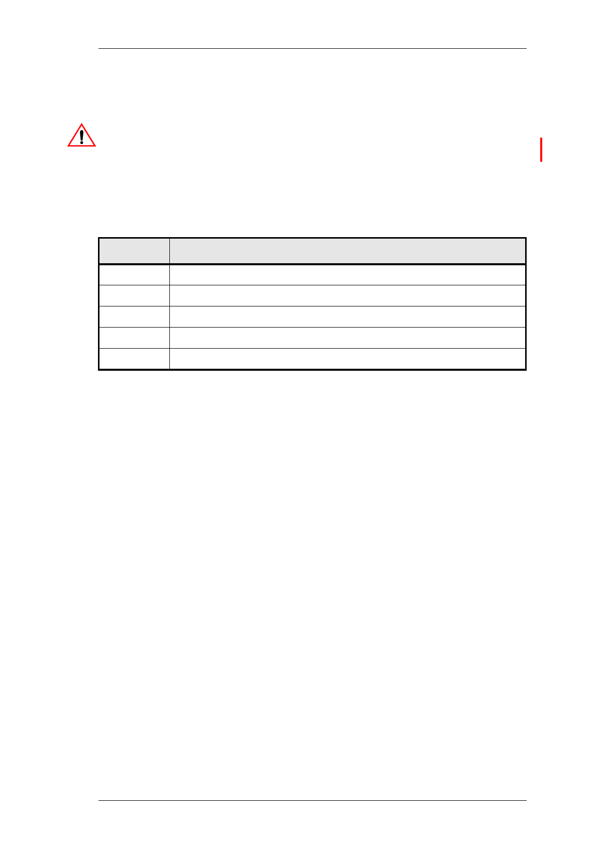
M830-00
DI
Copyright TEL 23/07/99
Part D T838 & T839 Power Amplifiers
Caution:
There are no user serviceable components in these power amplifiers.
Refer all servicing to your nearest Tait Dealer or Customer Service
Organisation.
This part of the manual is divided into five sections, as listed below. There is a detailed
table of contents at the start of each section.
Section Title
1 General Information
2 Circuit Operation
3 Initial Adjustment
4 Fault Finding
5 PCB Information


M830-00
T838/839 General Information
D1.1
Copyright TEL 30/04/98
1 T838/839 General Information
This section provides a brief description of the T838/839 PA, along with detailed specifi-
cations and a list of types available.
The following topics are covered in this section.
Section Title Page
1.1 Introduction 1.5
1.2
1.2.1
1.2.2
1.2.3
1.2.3.1
1.2.3.2
1.2.3.3
Specifications
Introduction
General
Test Standards
European Telecommunication Standard (ETS)
DTI CEPT Recommendation T/R-24-01
Telecommunications Industry Association
1.6
1.6
1.6
1.7
1.7
1.8
1.8
1.3 Product Codes 1.9
1.4 Standard Product Range 1.10
Figure Title Page
1.1
1.2
T838/839 Main Circuit Block Identification
T838/839 Front Panel Controls
1.4
1.4


M830-00
T838/839 General Information
D1.5
Copyright TEL 30/04/98
1.1 Introduction
The T838 & T839 are FM base station power amplifiers designed for single or multichan-
nel operation in the 136 to 174MHz frequency range. The typical output power capabil-
ities are as follows:
T838 - 10 to 60W
T839 - 20 to 120W.
The T838 PA comprises a single broad band RF power module whose output is filtered
before being fed to the output socket.
The T839 PA comprises two broad band RF power modules whose outputs are recom-
bined (using a quadrature hybrid combiner) and filtered before being fed to the output
socket. This dual module design enables the transmitter to produce at least one quarter
of its rated power if one of the modules fails.
VSWR and thermal protection is incorporated into the basic design, while monitoring
and alarm signals are available for both forward and reverse power. The output power
is adjustable from the front panel.
The main PCB is mounted directly on a die-cast chassis/heatsink. Extensive use is
made of the latest surface mount technology. Effective RF isolation between the PA con-
trol circuitry and RF stages is achieved by internal metal shields.
Forced air cooling for the heatsink is provided on the T839 by a fan, which is activated
whenever the transmitter is keyed. Thermal sensors will also activate the fan automati-
cally if the internal temperature reaches an unacceptable level.
The T838 has a width of 60mm and occupies a single space in a Tait rack frame, which
has the ability to accommodate up to seven standard modules. The T839 has a width of
120mm and occupies a double space.

D1.6
T838/839 General Information
M830-00
23/07/99 Copyright TEL
1.2 Specifications
1.2.1 Introduction
The performance figures given are minimum figures, unless otherwise indicated, for
equipment operating at standard room temperature (+22°C to +28°C) and standard test
voltage (13.8V DC).
Where applicable, the test methods used to obtain the following performance figures are
those described in the ETS specification. Refer to Section 1.2.3 for details of test stand-
ards.
Details of test methods and the conditions which apply for Type Approval testing in all
countries can be obtained from Tait Electronics Ltd.
1.2.2 General
Power Output:
T838 - Rated Power .. 50W
- Range Of Adjustment .. 10 to 60W (typical)
T839 - Rated Power .. 100W
- Range Of Adjustment .. 20 to 120W (typical)
Input Power .. 600mW to 1W
Duty Cycle Rating:
T838 .. 50W continuous to +60°C
T839 .. 100W continuous to +60°C
Intermodulation .. -70dBc or -40dBi1 with 25dB isolation
(PA with output isolator) & interfering signal of -30dBc
Mismatch Capability:
Ruggedness .. refer to your nearest Tait Dealer or
Customer Service Organisation
Stability .. 5:1 VSWR (all phase angles)
Supply Voltage:
Operating Voltage .. 10.8 to 16V DC
Standard Test Voltage .. 13.8V DC
Polarity .. negative earth only
Polarity Protection .. crowbar diode
1. dBi denotes the level of the intermodulation product relative to the interfering signal.

M830-00
T838/839 General Information
D1.7
Copyright TEL 23/07/99
Supply Current:
Standby .. 50mA
Transmit - T838 .. 11A (9A typical @ 156MHz)
- T839 .. 19A (15A typical @ 156MHz)
Spurious Emissions:
Conducted - Transmit .. -36dBm to 1GHz
-30dBm to 4GHz
- Standby .. -57dBm to 1GHz
-47dBm to 4GHz
Radiated - Transmit .. -36dBm to 1GHz
-30dBm to 4GHz
- Standby .. -57dBm to 1GHz
-47dBm to 4GHz
Operating Temperature Range .. -30°C to +60°C
Dimensions:
Height .. 183mm
Width - T838 .. 60mm
- T839 .. 120mm
Length .. 340mm
Weight:
T838 .. 3.2kg
T839 .. 3.4kg
1.2.3 Test Standards
Where applicable, this equipment is tested in accordance with the following standards.
1.2.3.1 European Telecommunication Standard
ETS 300 086 January 1991
Radio equipment and systems; land mobile service; technical characteristics and test
conditions for radio equipment with an internal or external RF connector intended pri-
marily for analogue speech.
ETS 300 113 March 1996
Radio equipment and systems; land mobile service; technical characteristics and test
conditions for radio equipment intended for the transmission of data (and speech) and
having an antenna connector.
ETS 300 219 October 1993
Radio equipment and systems; land mobile service; technical characteristics and test
conditions for radio equipment transmitting signals to initiate a specific response in the
receiver.

D1.8
T838/839 General Information
M830-00
30/04/98 Copyright TEL
ETS 300 279 February 1996
Radio equipment and systems; electromagnetic compatibility (EMC) standard for pri-
vate land mobile radio (PMR) and ancillary equipment (speech and/or non-speech).
1.2.3.2 DTI CEPT Recommendation T/R-24-01
Annex I: 1988
Technical characteristics and test conditions for radio equipment in the land mobile
service intended primarily for analogue speech.
Annex II: 1988
Technical characteristics of radio equipment in the land mobile service with regard to
quality and stability of transmission.
1.2.3.3 Telecommunications Industry Association
ANSI/TIA/EIA-603-1992
Land mobile FM or PM communications equipment measurement and performance
standards.

M830-00
T838/839 General Information
D1.9
Copyright TEL 23/07/99
1.3 Product Codes
The three groups of digits in the T830 Series II product code provide information about
the model, type and options fitted, according to the conventions described below.
The following explanation of T830 Series II product codes is not intended to suggest that
any combination of features is necessarily available in any one product. Consult your
nearest Tait Dealer or Customer Service Organisation for more information regarding
the availability of specific models, types and options.
Model
The Model group indicates the basic function of the product, as follows:
T83X-XX-XXXX T835 receiver
T836 25W transmitter
T837 exciter
T838 50W power amplifier
T839 100W power amplifier
Type
The Type group uses two digits to indicate the basic RF configuration of the product.
The first digit in the Type group designates the frequency range:
T83X-XX-XXXX ’1’ for 136-156MHz
’2’ for 148-174MHz
The second digit in the Type group indicates the channel spacing:
T83X-XX-XXXX ’0’ for wide bandwidth (25kHz)
’3’ for mid bandwidth (20kHz)
’5’ for narrow bandwidth (12.5kHz)
Options
T83X-XX-XXXX The Options group uses four digits and/or letters to indicate
any options that may be fitted to the product. This includes
standard options and special options for specific customers.
’0000’ indicates a standard Tait product with no options fitted.
The large number of options precludes listing them here.

D1.10
T838/839 General Information
M830-00
23/07/99 Copyright TEL
1.4 Standard Product Range
The following table lists the range of standard T838 and T839 types (i.e. no options fit-
ted) available at the time this manual was published. Consult your nearest Tait Dealer
or Customer Service Organisation for more information.
You can identify the PA type by checking the product code printed on a label on the rear
of the heatsink (Figure 1.1 in Part A shows typical labels). You can further verify the PA
type by checking the placement of an SMD resistor in the table that is screen printed
onto the PCB (refer to Section 5.1 for more details).
Output Power (W) 50 100
Frequency Range (MHz) 136-156 148-174 136-156 148-174
PA Type: T838- 10-0000 20-0000
PA Type: T839- 10-0000 20-0000

M830-00
T838/839 Circuit Operation
D2.1
Copyright TEL 23/07/99
2 T838/839 Circuit Operation
This section provides a basic description of the circuit operation of the T838/839 PA.
Refer to Section 5 where the parts lists, grid reference index and diagrams will provide
detailed information on identifying and locating components. Refer also to Figure 3.3
which shows the location of the main adjustment controls.
The following topics are covered in this section.
Section Title Page
2.1 Introduction 2.3
2.2 RF Circuitry 2.4
2.3
2.3.1
2.3.2
2.3.3
2.3.4
2.3.5
2.3.6
Control Circuitry
Power Control
Driver Power Level
Thermal Protection
Forward And Reverse Power Alarms
Forward And Reverse Power Metering
Fan Control Circuitry
2.5
2.6
2.6
2.6
2.7
2.7
2.7
2.4 Power Supply & Regulator Circuits 2.8
Figure Title Page
2.1
2.2
2.3
2.4
2.5
T838 High Level Block Diagram
T839 High Level Block Diagram
T838/839 Control Circuitry Block Diagram
T839 Fan Control Logic Diagram
T838/839 Power Supply & Regulator Circuitry Block Diagram
2.3
2.3
2.5
2.7
2.8

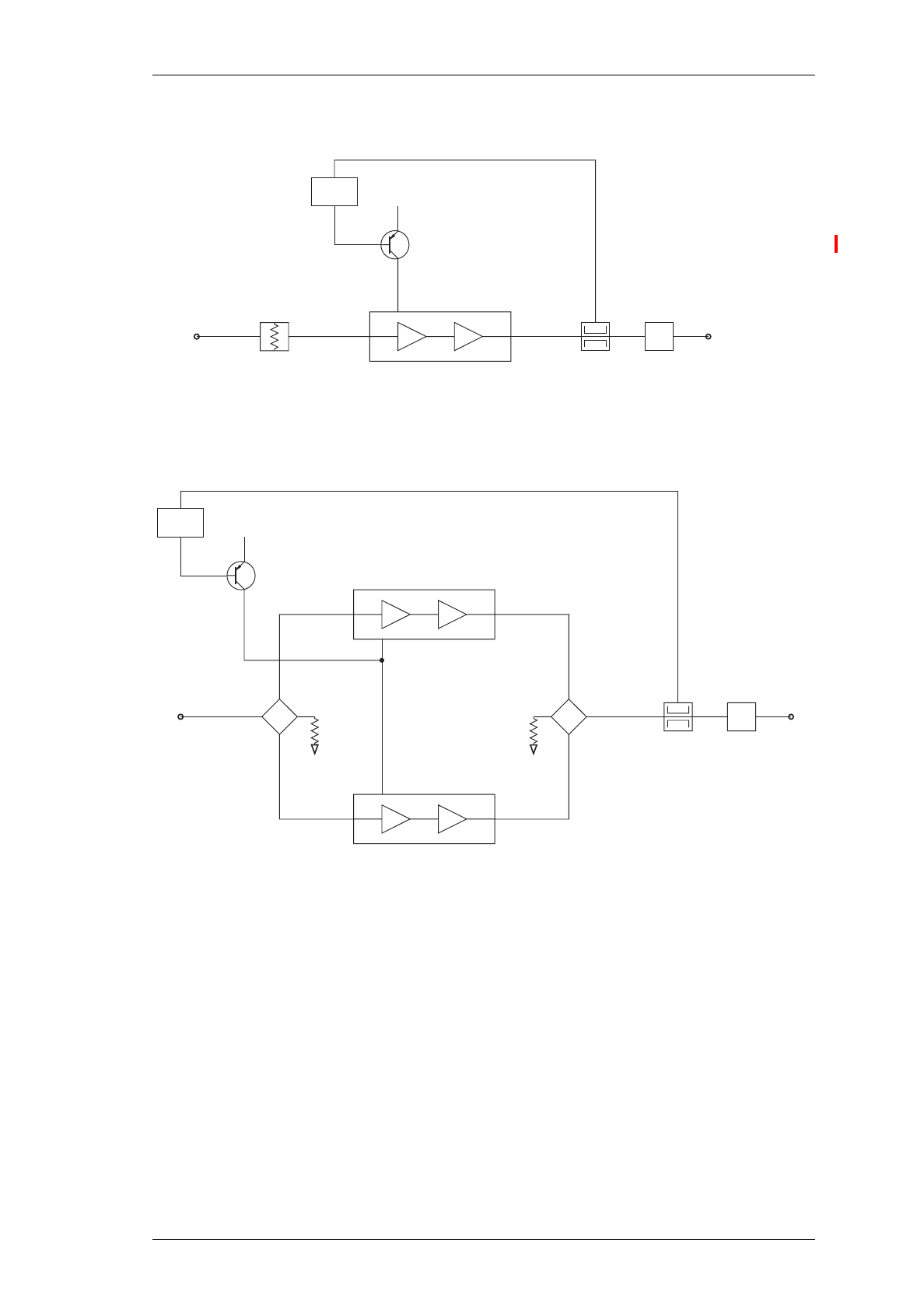
M830-00
T838/839 Circuit Operation
D2.3
Copyright TEL 23/07/99
2.1 Introduction
Figure 2.1 T838 High Level Block Diagram
Figure 2.2 T839 High Level Block Diagram
The T838/839 comprise a single stage RF power amplifier with extensive control cir-
cuitry:
• in the T838 this stage consists of a single, two-stage RF power module which
increases the drive level to approx. 60W;
• in the T839 this stage consists of two, two-stage RF power modules, each of
which increases the drive level to approx. 60W; the outputs from these mod-
ules are then combined to provide the rated output power.
Figure 2.1 and Figure 2.2 show the configuration of each of the main circuit blocks on a
functional level, while the fold-out Figure 1.1 shows their location on the PCB.
3dB Pad
RF Out
LPF
#IC201
M68702
400mW
(±100mW) 60W 50W
RF In
600mW - 1W
Power
Control Vsupply
Q137
Directional
Coupler
RF Out
LPF
#IC201
*#IC202
M68702
3dB Coupler 3dB Coupler
M68702
400mW
400mW 60W
60W
120W 100W
RF In
600mW - 1W
Power
Control Vsupply
Q317
*IC203 *IC205 Directional
Coupler

D2.4
T838/839 Circuit Operation
M830-00
30/04/98 Copyright TEL
2.2 RF Circuitry
(Refer to the RF & thermistor control sections circuit diagram in Section 5.)
The T838 consists of a single RF power module (#IC201) which delivers 60-70W. The
input signal is fed directly into the module, and the output from the module is passed to
the antenna socket via the directional coupler and low pass filter.
The T839 consists of two RF power modules (#IC201 & *#IC202), each of which delivers
60-70W. The input signal to these modules is split via a 3dB quadrature hybrid (*IC203).
The outputs from the modules are recombined by a second 3dB quadrature hybrid
(*IC205) before being passed to the antenna socket via the directional coupler and low
pass filter.
The directional coupler senses forward and reflected power, which is rectified (D201 &
D203) and passed to the control circuitry for metering, alarm and power control pur-
poses.
Power control is via a series pass transistor (Q137), which controls the supply voltage on
pin 2 of #IC201 in the T838, and pin 2 of both #IC201 and *#IC202 in the T839.
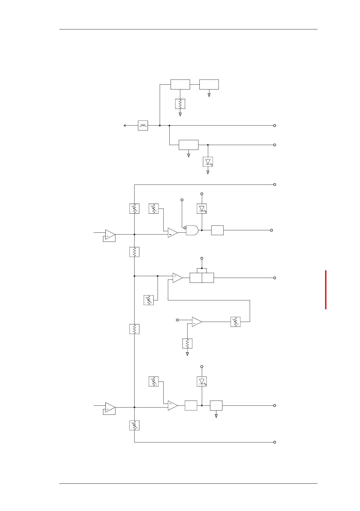
M830-00
T838/839 Circuit Operation
D2.5
Copyright TEL 23/07/99
2.3 Control Circuitry
(Refer to the control section circuit diagram in Section 5.)
Figure 2.3 T838/839 Control Circuitry Block Diagram
+
Comparator
Q129 Q131
FET
Switch
+
+
+
Comparator
FET
Switch
Q117
IC103
RV105
High Reverse Power LED
Low Forward Power LED
Reverse
Power
Meter
Reverse
Power
Alarm
Forward
Power
Meter
Forward
Power
Alarm
+7V
+7V
Tx
Key
IC103
RV101
RV103
+
+
Q137Q135
Q121
+13.8V
Filtered
Integrator
IC105
Control
Supply
-t° R237
NTC
RV109
Power
Control
Shutdown
Power Level
Comparator
IC101 RV113
R154
RV107
R153
Reverse
Power
Sense
Buffer
IC103
Buffer
IC103
Forward
Power
Sense
Ref.
7V
Supply
13.8V
Filtered
L101/L103
13.8V
RV115
Supply LED
IC109
IC107 IC105
Voltage
Regulator
Drive Level Clamp
Forward Power
Alarm
Reverse Power
Alarm
(RF Section)

D2.6
T838/839 Circuit Operation
M830-00
30/04/98 Copyright TEL
2.3.1 Power Control
The DC voltages from the directional coupler representing forward and reflected power
are buffered by the two voltage followers, IC103 pins 1, 2 & 3 and pins 8, 9 & 10. Their
outputs are summed at an integrator (IC105 pins 1, 2 & 3), which drives the series pass
control elements (Q135 & Q137).
Forward and reflected power are summed so that, under high output VSWR, the power
control turns the PA down. This is because the control loop adjusts for the same DC
voltage from the directional coupler that would have been present if there were no
reflected power.
2.3.2 Driver Power Level
The maximum output power of the T838/839 can be limited by placing a ceiling on the
driver output power level using RV115 (accessible through the side cover). For exam-
ple, if RV115 is set for a maximum output power of 50W, the range of adjustment using
RV109 (front panel power adjust) will be 20 to 50W.
Caution:
The driver power level clamp (RV115) is factory set to give a maximum
power output of 60W for the T838 and 120W for the T839. The unit may
be damaged if this level is increased.
2.3.3 Thermal Protection
At excessively high temperatures, the output power will automatically reduce to a pre-
set level (set by RV113), thus preventing the PA from overheating.
Ambient temperature within the PA is measured by a thermistor controlled voltage
divider (R168, R237) which applies a voltage to a comparator with hysteresis (IC101
pins 8, 9 & 10). This thermistor is located on the PCB in the low pass filter cavity.
Thermal protection is also provided for each RF power module to prevent the module
itself from overheating. This protection consists of a thermistor controlled voltage
divider (R207, *R215 and R220, R219) which sets a voltage on a comparator with hyster-
esis (IC204 pins 1, 2 & 3 and 5, 6 & 7). These thermistors are located on the module
flanges.
The output current from all comparators is summed into the power control network via
RV113 so that the power level to which the PA must turn down may be set.
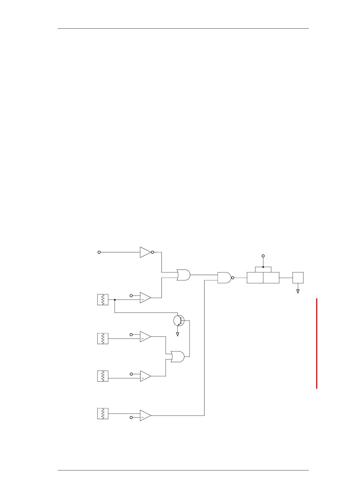
M830-00
T838/839 Circuit Operation
D2.7
Copyright TEL 23/07/99
2.3.4 Forward And Reverse Power Alarms
If forward power drops below, or reverse power rises above, presettable limits, alarms
may be triggered.
The alarm outputs are open drain configuration and are low under normal conditions
(i.e. forward and reverse power levels are normal).
IC103 pins 12, 13 & 14 and pins 5, 6 & 7 form comparators with thresholds adjusted via
RV101 and RV105 respectively. The inputs are from the forward and reverse power sig-
nals from the directional coupler, buffered by IC103 pins 1, 2 & 3 and pins 8, 9 & 10.
Thus, the power levels at which the forward and reverse power alarms are triggered are
defined by RV101 and RV105 respectively.
2.3.5 Forward And Reverse Power Metering
Forward and reverse power signals from the two IC1 buffers are available for metering
purposes. The output currents are adjustable via RV103 (forward power) and RV107
(reverse power).
2.3.6 Fan Control Circuitry
Figure 2.4 T839 Fan Control Logic Diagram
*Q107 *Q109 Fan
Ref +
Ref +
High Temp.
Sense On PCB
Comparator
IC101
R237
High Temp.
Sense On
Module Flange
High Temp.
Sense On
Module Flange
Comparator
IC204
Ref +
Comparator
IC204
*R215
R219
NTC
NTC
Low Temp.
Sense
Comparator
Ref +
IC101
*R116
NTC
NTC
Tx Key
Invert
*Q101 OR
*Q103,
*R106, *R107
OR
Q201
D202, R212,
R214
NAND
*Q103, *Q105,
*R111, *R112 Fan Driver
13.8V
Filtered
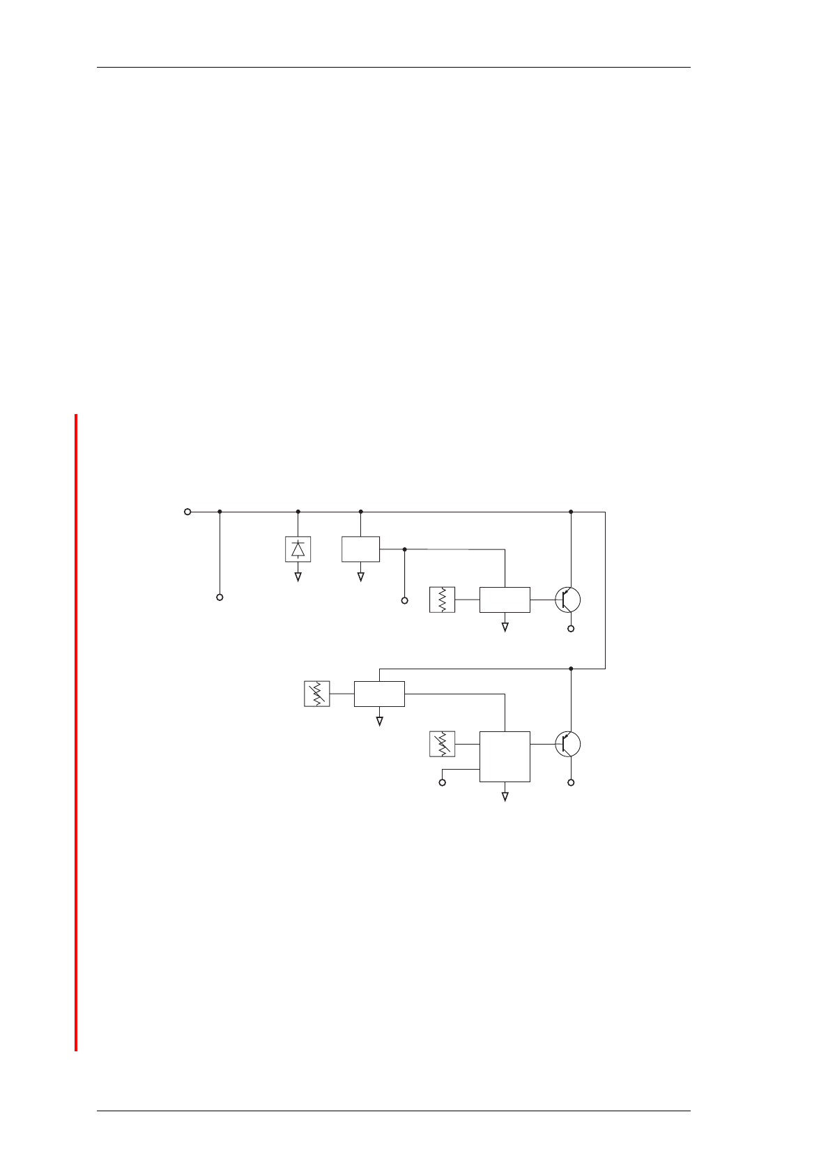
D2.8
T838/839 Circuit Operation
M830-00
23/07/99 Copyright TEL
Comparator IC101 pins 12, 13 & 14 are set to switch at heatsink temperatures greater
than +90°C or RF power module flange temperatures greater than +110°C, and pins 1, 2
& 3 at temperatures less than -10°C.
A logic AND function is applied to the comparator outputs by *Q103 and *Q105,
thereby turning on the fan unconditionally (via *Q107 and *Q109) if the heatsink tem-
perature exceeds +90°C or the module flange temperatures exceed +110°C.
A logic OR function is applied to comparator IC101 pins 12, 13 & 14 and Tx KEY signals,
thereby turning on the fan when the transmitter is keyed and the temperature is
between -10°C and +90°C (or +110°C for the module flanges).
If the temperature drops below -10°C, *Q105 is turned off, preventing *Q103 from acti-
vating the fan.
2.4 Power Supply & Regulator Circuits
(Refer to the control section circuit diagram in Section 5.)
Figure 2.5 T838/839 Power Supply & Regulator Circuitry Block Diagram
The T838/839 are designed to operate off a 10.8-16V DC supply (13.8V nominal). A 7V
supply runs directly off the 13.8V rail, driving the fan control, power control and alarm
circuitry.
A crowbar diode is fitted for protection against connection to a power supply of incor-
rect polarity. It also provides transient overvoltage protection.
Note:
A fuse must be fitted in the power supply line for the diode to provide effec-
tive protection.
7V
Reg.
Fan
Control
Power
Clamp
Power
Control
Crowbar
Diode
Temp.
Sense
To Fan
+7V
Clamp
Power
From
Directional
Coupler
Power
Control
Vout
Set
Power
13.8V
Nom.
M830-00
T838/839 Initial Adjustment
D3.1
Copyright TEL 23/07/99
3 T838/839 Initial Adjustment
Caution:
This equipment contains CMOS devices which are susceptible to dam-
age from static charges. Refer to Section 1.2 in Part A for more infor-
mation on anti-static procedures when handling these devices.
The following section describes the full adjustment procedure to be carried out before
operating the T838/839.
Note:
The T838/839 require no RF tuning or alignment.
Refer to Section 5 where the parts lists, grid reference index and diagrams will provide
detailed information on identifying and locating components. Refer also to Figure 3.3
which shows the location of the main adjustment controls.
The following topics are covered in this section.
Section Title Page
3.1 Test Equipment Required 3.3
3.2 Preliminary Checks 3.3
3.3 Setting The Output Power 3.4
3.4 Limiting The Maximum Output Power 3.5
3.5 High Temperature Shutdown Power Level 3.5
3.6 Remote Forward Power Meter Calibration 3.6
3.7 Remote Reverse Power Meter Calibration 3.6
3.8
3.8.1
3.8.2
Setting Alarm Levels
Forward Power
Reverse Power
3.6
3.6
3.6
Figure Title Page
3.1
3.2
3.3
T838/839 Test Equipment Set-up
Modifications To Limit Maximum Output Power
T838/839 Main Adjustment Controls
3.3
3.5
3.9

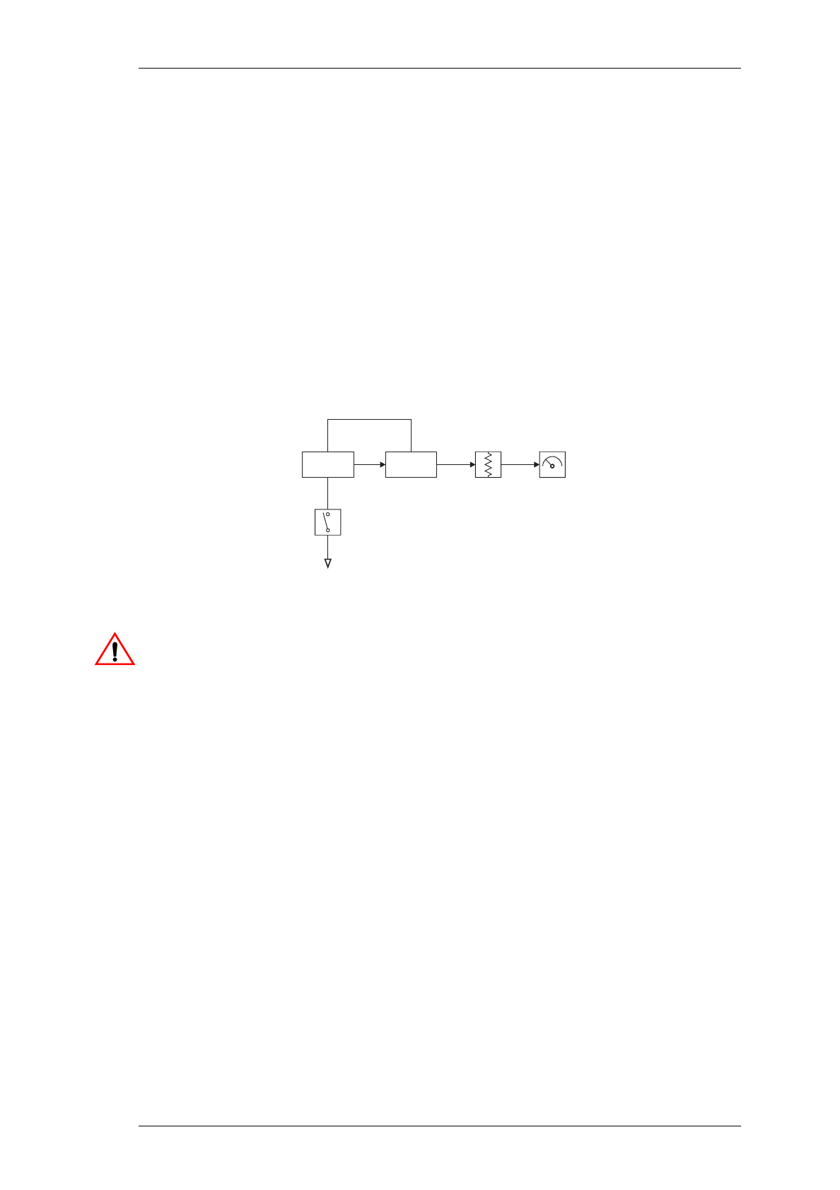
M830-00
T838/839 Initial Adjustment
D3.3
Copyright TEL 30/04/98
3.1 Test Equipment Required
• DC power supply capable of delivering 30A at 13.8V.
• Multimeter or DMM (e.g. Fluke 77).
• RF power meter (e.g. HP 435 series or Bird Wattmeter).
• 150W 30dB attenuator.
• 150W 3dB 50 ohm pad.
• 'BNC' to 'N' type adaptors (e.g. Amphenol, Greenpar).
• Appropriate trimming tools.
Figure 3.1 T838/839 Test Equipment Set-up
Caution:
Do not connect attenuators or DC blocks between the T837 and T838/
839 or the cyclic keying circuitry will not function correctly.
3.2 Preliminary Checks
Check for short circuits between the positive rail and earth.
Set up the test equipment as in Figure 3.1.
Connect the T838/839 to a 13.8V DC supply.
Check that the quiescent current is <50mA.
To key the transmitter, earth the key line (pin 13) on the exciter.
Check that the power supply is still at 13.8V under load.
Check that the regulated power control supply is approximately 7V.
Note:
The output power and alarm levels should be set with the side cover on. If
the cover is removed for other adjustment procedures, make a final check of
the output power and alarm levels with the side cover on.
Exciter PA
Tx Key
RF Power
Meter
Tx Enable
30db
Attenuator
(HP 435)

D3.4
T838/839 Initial Adjustment
M830-00
30/04/98 Copyright TEL
3.3 Setting The Output Power
Caution:
If the high temperature shutdown power level has not yet been set or is
unknown, check that the unit does not overheat while setting the out-
put power.
Note 1:
Cables and connectors can easily cause a power loss of several watts if either
too long or poorly terminated. Always use the shortest possible leads (or
connectors instead of leads) between the T838/839 and power meter set-up.
Note 2:
You will need appropriate extension leads if you wish to carry out the
adjustment procedures with the T838/839 withdrawn from the rack in the
latched position. Alternatively, disconnect and withdraw the T838/839 and
reconnect it behind the rack.
Note 3:
The actual power used may be limited by regulatory requirements.
Connect the exciter output to the PA input via a thru-line wattmeter with a 1W
full scale reading. Special BNC/N leads will be required.
Connect an RF power meter to the PA output.
Set the front panel power control preset (RV109) fully clockwise.
Key on the drive source.
Check that the power output exceeds:
T838 - 50W
T839 - 100W.
Note:
The side cover access hole for the driver power clamp (RV115) is covered
with a tamper-proof sticker. The clamp has been factory set to 60W (T838)/
120W (T839) maximum output power and should not normally need
adjustment. If the output power level is low, check that the high tempera-
ture shutdown circuit has not activated by verifying that IC101 pin 8 is low.
Adjust RV109 to set the power output to the required level (e.g. 50W for the T838,
100W for the T839).
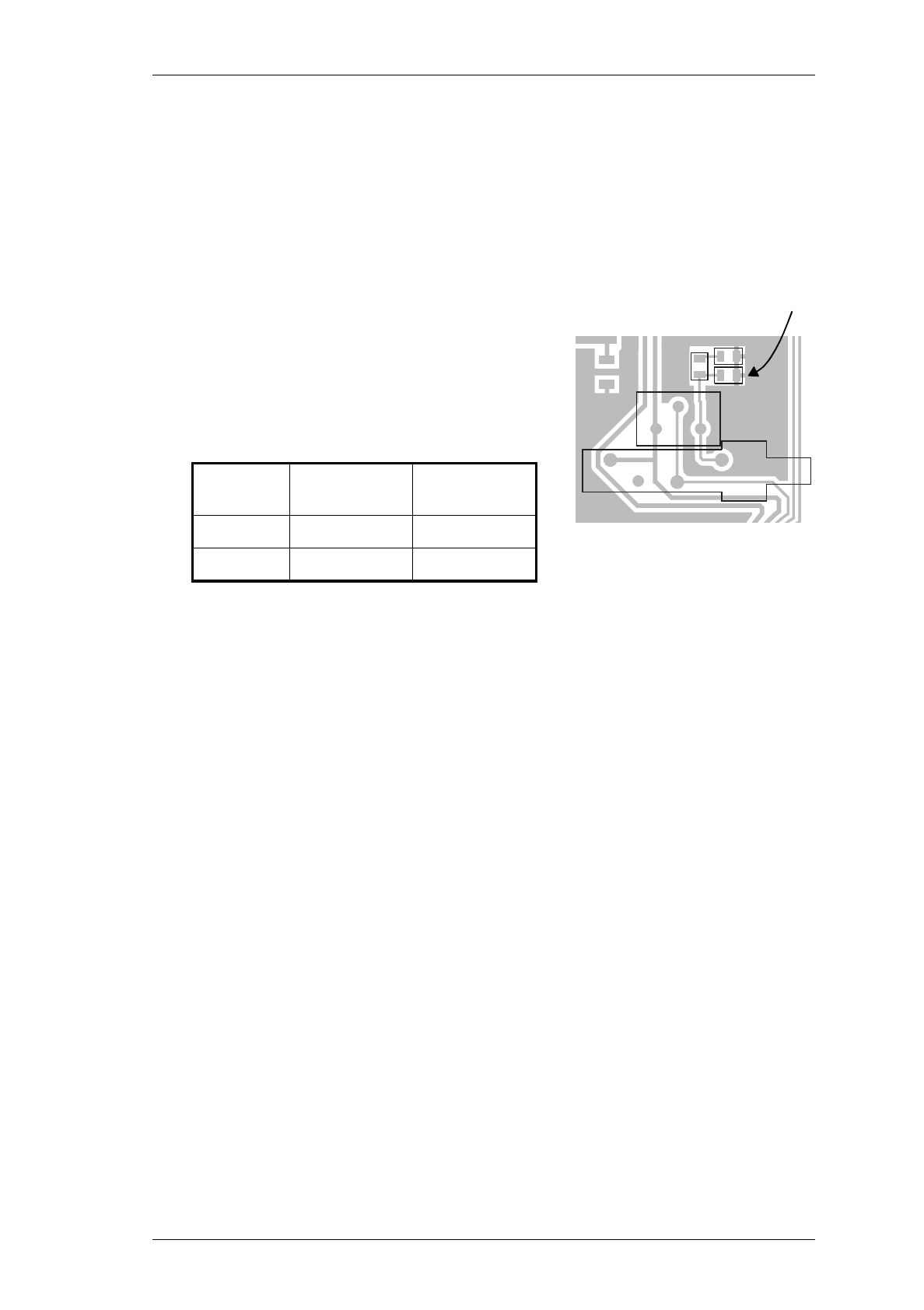
M830-00
T838/839 Initial Adjustment
D3.5
Copyright TEL 30/04/98
3.4 Limiting The Maximum Output Power
Refer to the control section circuit diagram in Section 5.
Two chip resistors are provided on the PCB if there is a requirement to set an absolute
limit to the maximum output power. These two resistors are normally bypassed by a
zero Ohm resistor (LINK2).
Note:
The resistor values given in the above table are valid at 174MHz only. Dif-
ferent frequencies may require different values, and you will have to deter-
mine the correct values for your application by testing. At any given
frequency an increase in resistance will result in a decrease in maximum
output power.
3.5 High Temperature Shutdown Power Level
Set RV109 (power control) to the required output power.
Earth pin 9 of IC101 (the via at NTC R237 is convenient).
Adjust RV113 (shutdown power level) for an output power of:
T838 - 16W
T839 - 40W.
Remove the earth from pin 9 of IC101 (or the pad of R237).
To check the operation of the RF power module thermistor(s), place shorting links
across pins 1 & 2 and 2 & 3 of LINK201.
Check that the output power drops to:
T838 - 16W
T839 - 40W.
Remove the shorting links from LINK201.
*RV111
LINK2
R173
R174
RV109
Remove LINK2 as shown in Figure 3.2 to
bring R173 & R174 into circuit.
You can now limit the maximum output
power by selecting the appropriate values
for R173 & R174. Two examples are given in
the table below:
@174MHz 60W max.
(T838 & T839) 110W max.
(T839 only)
R173 470Ω470Ω
R174 3k9 1k8
Figure 3.2 Modifications To Limit
Maximum Output Power
remove LINK2 to bring
R173 & R174 into circuit

D3.6
T838/839 Initial Adjustment
M830-00
30/04/98 Copyright TEL
3.6 Remote Forward Power Meter Calibration
If a remote meter is connected, adjust the forward power meter calibration control
(RV103) for the remote reading to agree with the RF power meter reading.
3.7 Remote Reverse Power Meter Calibration
If a remote meter is connected, connect a 50 ohm 3dB pad (with the output open
circuit) to the PA output.
Apply RF drive and Tx key.
Adjust the reverse power meter calibration control (RV107) for a quarter of the for-
ward power reading.
3.8 Setting Alarm Levels
Note:
If forward and reverse power metering is being used, set up their calibration
(Section 3.6 and Section 3.7) before setting the alarm levels.
3.8.1 Forward Power
Power up the T838/839 and adjust the front panel power control (RV109) so that
the output power is at the alarm level required (e.g. 80W if the T839 normally
operates at 100W).
Adjust the forward power alarm set control (RV101) so that the forward power
alarm LED lights.
Check the alarm level setting by adjusting the power up and down and observing
the alarm LED. A few watts hysteresis can be expected.
Readjust RV109 for the normal operating level.
Note:
Remote indication is available at pin 3 of D-range 1.
3.8.2 Reverse Power
Power up the T838/839 and adjust the front panel power control (RV109) for the
normal operating power level.
Place a known mismatch of the required value (e.g. 3:1 VSWR) and adjust the
reverse power alarm set control (RV105) so that the reverse power alarm LED
lights.


M830-00
T838/839 Fault Finding
D4.1
Copyright TEL 23/07/99
4 T838/839 Fault Finding
Caution:
This equipment contains CMOS devices which are susceptible to dam-
age from static charges. Refer to Section 1.2 in Part A for more infor-
mation on anti-static procedures when handling these devices.
The following test procedures and fault finding flow charts may be used to help locate a
hardware problem, however they are by no means a complete fault finding procedure.
If you still cannot trace the fault after progressing through them in a logical manner,
contact your nearest Tait Dealer or Customer Service Organisation. If necessary, you can
get additional technical help from Customer Support, Radio Systems Division, Tait Elec-
tronics Ltd, Christchurch, New Zealand (full contact details are on page 2).
Refer to Section 5 where the parts lists, grid reference index and diagrams will provide
detailed information on identifying and locating components.
The following topics are covered in this section.
Section Title Page
4.1 Visual Checks 4.3
4.2 DC Checks 4.3
4.3 RF Checks 4.3
4.4
4.4.1
4.4.2
4.4.3
4.4.4
Fault Finding Charts
T838 PA
T839 PA
Power Control
Fan Control Circuitry
4.7
4.7
4.8
4.9
4.10
4.5 Replacing RF Power Modules 4.11
4.6 Removing The PCB From The Heatsink 4.12
Figure Title Page
4.1 Positioning Of Test Leads 4.6


M830-00
T838/839 Fault Finding
D4.3
Copyright TEL 30/04/98
4.1 Visual Checks
Remove the side cover from the T838/839 and inspect the PCB for damaged or
broken components, paying particular attention to the surface mounted devices
(SMDs). Also check for defective solder joints.
Refer to Section 4.5, Section 4.6 and Section 3 of Part A for more details on repair
and replacement of components.
4.2 DC Checks
Check that +13.8V is present on pin 3 of *#IC202 and/or #IC201. Make this meas-
urement when the transmitter is not keyed.
Check that approximately 6-13V is present on pin 2 of *#IC202 and/or #IC201 (the
level is dependent on the setting of RV109).
Check that +13.8V is present at pin 4 of IC103.
Check that approximately +12V is present at pin 8 of IC105 (the level is dependent
on the setting of RV109).
Check that +7.0V is present at the output of regulator IC109.
4.3 RF Checks
The PA Fault Finding Charts (Section 4.4.1 & Section 4.4.2) provide a systematic
approach for locating a fault in the RF circuitry. Use these charts in conjunction with
Figure 4.1, which shows the locations of the 50Ω input and output test points for RF
power modules #IC201 and *#IC202.
Note 1:
Use good quality 50Ω coax for the "flying" test leads.
Note 2:
Ensure each output is terminated in a 50Ω load of the correct power rating.
For problems with the power control circuitry, refer to the Power Control Fault Finding
Chart (Section 4.4.3).


M830-00
T838/839 Fault Finding
D4.7
Copyright TEL 30/04/98
4.4 Fault Finding Charts
4.4.1 T838 PA
RF circuitry OK.
N
Y
Y
Is RV109
fully clockwise? Rotate RV109
fully clockwise.
Y
Is RV115
fully clockwise? Rotate RV115
fully clockwise.
N
N
Is maximum power >50W
over entire frequency range?*
Earth D-range pin 12 or
connect to exciter key line.
N
Y
*Frequency Ranges
T838-10: 136-156MHz
T838-20: 148-174MHz
Is the drive from the
exciter 600mW-1W? Set drive to
600mW-1W.
Is the output from
#IC201 >60W?
Refer to Figure 4.1.
NCheck #IC201 solder joints.
If joints OK, replace module.
Check components in LPF.
Check output N-type connector
for short circuit or excessive wear.
Replace parts as necessary.
Is maximum power >50W
over entire frequency range?*
N
Return PA to your local
Tait service centre.
Y
Is #IC201 pin 2 >10V?
Is #IC201 pin 3 >13V?
Replace Q135 & Q137,
then check #IC201 pin 2
for short circuit.
Y
Y
N
N
Set RV115 to 60W
(driver power clamp).
Set RV109 to required
output power.
Refer to Section 3.3.
Is the PA keyed?
(D-range pin 12 low)
Y
D4.8
T838/839 Fault Finding
M830-00
30/04/98 Copyright TEL
4.4.2 T839 PA
RF circuitry OK.
N
Y
Y
Is RV109
fully clockwise? Rotate RV109
fully clockwise.
Y
Is RV115
fully clockwise? Rotate RV115
fully clockwise.
Is maximum power >100W
over entire frequency range?*
N
N
Return PA to your local
Tait service centre.
N
Is maximum power >100W
over entire frequency range?*
Y
*Frequency Ranges
T839-10: 136-156MHz
T839-20: 148-174MHz
Replace splitter hybrid.
Check the condition of
splitter hybrid *IC203.
Are there any shorts
on the legs or broken legs?
Y
N
Replace combiner hybrid.
Check the condition of
combiner hybrid *IC205.
Are there any shorts
on the legs or broken legs?
N
Y
Y
N
Is the output from #IC201
and *#IC202 >60W per module
(measured concurrently)?
Refer to Figure 4.1.
Check #IC201/*#IC202 solder joints.
If joints OK, replace module(s).
Check components in LPF.
Check output N-type connector
for short circuit or excessive wear.
Replace parts as necessary.
N
Is *R223 hot to touch
when PA keyed? Y
Set RV115 to 120W
(driver power clamp).
Set RV109 to required
output power.
Refer to Section 3.3.
N
Y
Is the drive from the
exciter 600mW-1W? Set drive to
600mW-1W.
Earth D-range pin 12 or
connect to exciter key line.
Y
NIs the PA keyed?
(D-range pin 12 low)
Is #IC201/*#IC202 pin 2 >10V?
Is #IC201/*#IC202 pin 3 >13V? NReplace Q135 & Q137,
then check #IC201/*#IC202
pin 2 for short circuit.
Y
M830-00
T838/839 Fault Finding
D4.9
Copyright TEL 30/04/98
4.4.3 Power Control
Approximate voltages (@ 174MHz) under normal operating conditions:
Forward & Reverse Power
Measurement
Output Power
50W 100W
forward power at IC103 pin 1
forward power at C261
reverse power at IC103 pin 8
reverse power at C294
2.3V
4.1V
0.6V
0.3V
3.3V
6.0V
0.6V
0.6V
N
Check 12V DC present
on IC105 pin 8.
Check sense voltages
from directional coupler.
Check IC103 pins 1 & 8.
RF Power Level Control Check
Check Q117 & Q121.
Check IC103 pin 14 >12V DC
when forward power low.
Low Forward Power Alarm Check
Y
Y
N
Does high reverse power alarm
LED light when PA operated into
a mismatch of 3:1 or worse?
Check Q129 & Q131.
Check IC103 pin 7 >12V DC
when reverse power high.
High Reverse Power Alarm Check
N
Y
Earth IC101 pin 9.
Check IC103 pin 13 is at 0.6V.
Check IC103 pin 14 goes from
high to low when IC101 pin 9
is earthed. Check Q133.
Y
Over-Temperature Shutdown Check
N
Power control OK.
Using RV109, does output power
adjust over the range:
At high operating temperatures,
does the output power reduce to:
Using RV109, does low forward
power alarm LED light when
output power reduced to:
The following voltage checks are all done with
RV115 (driver power clamp) set to maximum.
When these tests are finished, reset RV115
to 60W (T838) or 120W (T389).
Caution
T838 10-60W
T839 20-120W?
T838 40W
T839 80W?
T838 14W
T839 40W?
Note:
A final confirmation of high temperature
shutdown and/or T839 fan activation at
high temperatures can be obtained by
heating the earth pad of R237 to >130°C
with the tip of a soldering iron. Take care
not to damage R237.
D4.10
T838/839 Fault Finding
M830-00
30/04/98 Copyright TEL
4.4.4 T839 Fan Control Circuitry
Y
Y
Y
Key transmitter.
Does fan run at
room temperature?
Does the low temperature
inhibit circuit stop the fan?
Do not key
transmitter.
Earth IC101 pin 9
(see Section 3.5).
Does hi
g
h temperature control
circuit activate fan?
Fan control OK.
Earth IC101 pin 9
(see Section 3.5).
Check IC101 pin 14 >11V.
Check *Q105 & *Q103.
N
N
N
Spray "freeze" on *R116
OR short R118.
Check IC101 pin 1 >11V.
Check *Q105 & *Q103.
Spray "freeze" on *R116
OR short R118.
Check *Q103 & *Q105
collector volta
g
es.
Check *Q107 & *Q109.
Check IC101 pin 1 <1V.
Check *Q101.
Check Tx-key is low (at
g
round).

M830-00
T838/839 Fault Finding
D4.11
Copyright TEL 23/07/99
4.5 Replacing RF Power Modules
Caution:
Follow these instructions carefully, otherwise the module can fail
because of poor heatsinking or cracked substrates.
Caution:
Do not apply too much heat to the original type of thermistor assembly
as the epoxy used may give off fumes that will cause eye irritation. If
necessary, replace this device as a complete assembly (see note 1 below).
Desolder the module and thermistor1 legs by heating with a soldering iron and
lifting away from the PCB with a screwdriver or thin stainless steel spike.
Undo the module screws and remove the thermistor assembly.
Desolder and remove both earth tags.
Gently lift the module away from the heatsink.
Note:
The module may be stuck down quite firmly with heatsink compound. You
may need to carefully prise it away from the heatsink with a small screw-
driver. Keep the heatsink compound clean while the module is detached.
Apply a small amount of heatsink compound (Dow-Corning 340 or equivalent) to
the replacement module mounting surface. Use enough compound to ensure an
even film over the entire mounting surface.
Reposition the module in the correct orientation and ensure it is well pasted to the
heatsink.
Replace the earth tags and thermistor1 assembly in their original positions and
hand-tighten the screws, ensuring the tags and thermistor remain in place. Alter-
nately tighten each screw evenly, finally torquing them down to 56N.cm/5in.lbf.
with an accurate torque driver.
Caution:
It is essential that you apply the correct torque to these screws to allow
the module flange to expand and contract under temperature cycling.
Also, do not solder any module legs before torquing down otherwise
the device may be broken.
Solder all module legs to the PCB.
Carefully solder the thermistor leg to the PCB1.
1. Later production PAs are fitted with a different type of thermistor which you
do not need to desolder from the PCB before removing a power module. Refer
to the top side PCB layout diagrams in Sections 5.2 and 5.3 for further details.

D4.12
T838/839 Fault Finding
M830-00
30/04/98 Copyright TEL
4.6 Removing The PCB From The Heatsink
Note:
This is a lengthy procedure and should be considered only after all other
checks have been carried out. There are no components on the bottom of the
PCB.
Remove the harmonic filter shield lid.
T839 Only: Desolder the power feed to the fan from the PCB.
Remove the output 50 ohm coaxial connector by unscrewing it from the heatsink
casting and desoldering it from the PCB and harmonic filter shield wall.
Unplug the input 50 ohm coaxial cable from the PCB, unscrew the BNC connector
from the heatsink, and remove the connector and cable.
Desolder the positive and negative power feed wires from the D-range PCB.
Disconnect the ribbon cable from the D-range PCB.
Remove the 2 screws securing the D-range connector and PCB to the heatsink and
withdraw the assembly from the heatsink.
Remove the mounting screws for the TO-220 device(s): Q137 (and *R223 in the
T839).
Remove the screws securing the RF power module(s): #IC201 (and *#IC202 in the
T839).
T839 Only: Remove the four hex nuts and washers from the splitter/com-
biner hybrids (*IC203 and *IC205).
Remove the 11 PCB retaining screws.
Push the three LEDs out of their front panel grommets.
Lift the PCB gently from the heatsink to gain access to the underside of the board.
Note:
#IC201, *#IC202 and *R223 may be stuck down with heatsink compound.
You may need to carefully prise them away from the heatsink with a small
screwdriver.
Caution:
Keep the heatsink compound clean while the PCB is detached. Any
objects caught in the heatsink compound underneath the module
which prevent effective earthing and/or heatsinking will cause cata-
strophic failure.
Caution:
Do not operate the PA with the PCB detached as the heatsink is used
for earthing and heat dissipation.

M830-00
T838/839 Fault Finding
D4.13
Copyright TEL 23/07/99
To replace the PCB, reverse the order of removal, taking care that the wiring is cor-
rectly positioned and not 'pinched'.
Make sure that the heatsink compound has stayed clean, and that the insulating
pad for Q137 is not damaged.
If you have difficulty refitting the LEDs, try pushing the body of the LED back
into the grommet with a thin screwdriver or spike.
Caution:
Tighten the splitter/combiner hybrid hex nuts to a torque of 22N.cm/
2in.lbf. Any greater force will damage the devices.
Tighten the RF power module screws to a torque of 56N.cm/5in.lbf.
with an accurate torque driver. Deviating from this figure can cause
the device to fail (refer to Section 4.5).

M830-00
T838/839 PCB Information
D5.1.1
Copyright TEL 23/07/99
5 T838/839 PCB Information
Caution:
This equipment contains CMOS devices which are susceptible to damage from
static charges. Refer to Section 1.2 in Part A for more information on anti-static
procedures when handling these devices.
This section provides the following information on the T838 and T839 power amplifiers:
•parts lists
• grid reference indexes
• mechanical assembly drawings
•PCB layouts
• circuit diagrams.
The T838 and T839 share the same basic design and are built on the same PCB. However, in order to
simplify the presentation of the PCB information for each product, we have provided a separate
parts list, grid reference index and set of drawings for both the T838 and T839, even though this has
meant duplicating some information (e.g. grid reference index and circuit diagrams) in each section.
Section Title IPN Page
5.1 Introduction 5.1.3
5.2 T838 Power Amplifier PCB 220-01404-03 5.2.1
5.3 T839 Power Amplifier PCB 220-01404-03 5.3.1

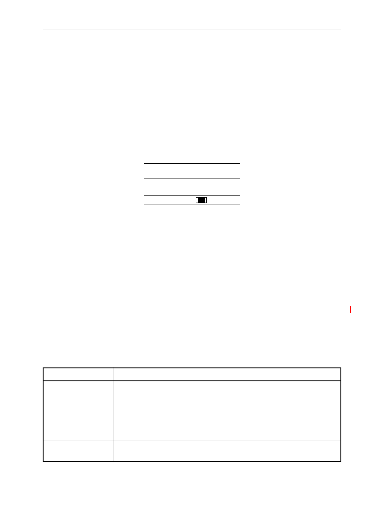
M830-00
T838/839 PCB Information
D5.1.3
Copyright TEL 23/07/99
5.1 Introduction
Product Type Identification
You can identify the PA type by checking the product code printed on a label on the rear of the heat-
sink (product codes are explained in Section 1.3 in this Part of the manual, and Figure 1.1 in Part A
shows typical labels). You can further verify the PA type by checking the placement of an SMD
resistor in the table that is screen printed onto the PCB, similar to the example drawn below. In this
example, the resistor indicates that the product was built as a T830 Series I compatible
T838-10-XXXX. See below for further details on T830 Series I/Series II compatibility.
T830 Series I / Series II Compatibility
T838 and T839 PAs can be built compatible with either T830 Series I or Series II equipment. You can
check whether your PA was built as Series I or Series II compatible by checking the table that is
screen printed onto the PCB, as explained above.
The table below explains briefly the differences between Series I and Series II compatible PAs.
Apart from these differences, Series I and Series II compatible PAs are electrically and mechanically
the same. Refer to Part I for detailed information on Series I/Series II compatibility.
Note:
This manual covers the latest design T838 PA which uses an RF power module and is
identified by the product code T838-X0-XXXX. Please refer to service manual
M830-00-100 for information on the earlier model (Series I) T838 PA which is identified
by the product code T838-10.
Item Series I Compatible PA Series II Compatible PA
*L201 (T838)
*L211 (T839) not fitted fitted
*R120 fitted not fitted
cyclic keying disabled enabled
RF input front panel SMC rear panel BNC
front panel Series I with black Tait logo
and Series I handle Series II with blue Tait logo
and Series II handle
PRODUCT TYPE
MODEL REV SERIES
I
SERIES
II
T839-10 3A
T839-20 3A
T838-10 3A
T838-20 3A
Note:
The only function of this
resistor is to indicate the
product type. It has no
effect on the circuitry or
operation of the PA.
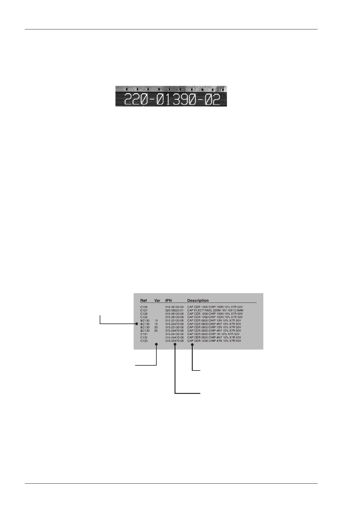
D5.1.4
T838/839 PCB Information
M830-00
30/04/98 Copyright TEL
PCB Identification
All PCBs are identified by a unique 10 digit “internal part number” (IPN), e.g. 220-12345-00, which
is screen printed onto the PCB (usually on the top side), as shown in the example below:
The last 2 digits of this number define the issue status, which starts at 00 and increments through 01,
02, 03, etc. as the PCB is updated. Some issue PCBs never reach full production status and are there-
fore not included in this manual. A letter following the 10 digit IPN has no relevance in identifying
the PCB for service purposes.
Note:
It is important that you identify which issue PCB you are working on so that you can
refer to the appropriate set of PCB information.
Parts Lists
The 10 digit numbers (000-00000-00) in this Parts List are “internal part numbers” (IPNs). We can
process your spare parts orders more efficiently and accurately if you quote the IPN and provide a
brief description of the part.
The components listed in this parts list are divided into two main types: those with a circuit refer-
ence (e.g. C2, D1, R121, etc.) and those without (miscellaneous and mechanical).
Those with a circuit reference are grouped in alphabetical order and then in numerical order within
each group. Each component entry comprises three or four columns, as shown below:
The mechanical and miscellaneous section lists the variant and common parts in IPN order.
circuit reference -
lists components
in alphanumeric
order
variant column -
indicates that this is
a variant component
which is fitted only to
the product type listed
Internal Part Number -
order the component
by this number
description -
gives a brief description
of the component
M830-00
T838/839 PCB Information
D5.1.5
Copyright TEL 30/04/98
Parts List Amendments
At the front of the parts list is the Parts List Amendments box (an example of which is shown
below). This box contains a list of component changes which took place after the parts list and dia-
grams in this section were compiled. These changes (e.g. value changes, added/deleted compo-
nents, etc.) are listed by circuit reference in alphanumeric order and supersede the information
given in the parts list or diagrams. Components without circuit references are listed in IPN order.
The number in brackets at the end of each entry refers to the Tait internal Change Order document.
Variant Components
A variant component is one that has the same circuit reference but different value or specification in
different product types. Where two products share the same PCB, the term “variant” is also used to
describe components unplaced in one product. Variant components have a character prefix, such as
“&”, “=” or “#”, before the circuit reference (e.g. &R100).
The table below explains the variant prefixes used in T800 Series II products:
If the variant prefix is. . . the component will. . .
& change according to channel spacing
= change according to frequency stability
# change according to frequency range
% be placed or unplaced for special applications
*be unplaced in one product
(where two products share the same PCB)
Parts List Amendments
R306 Changed from 180Ωto 560Ω(036-13560-00) to increase sensitivity (71003).
circuit reference
or IPN description
of change
IPN of new
component Change Order
number
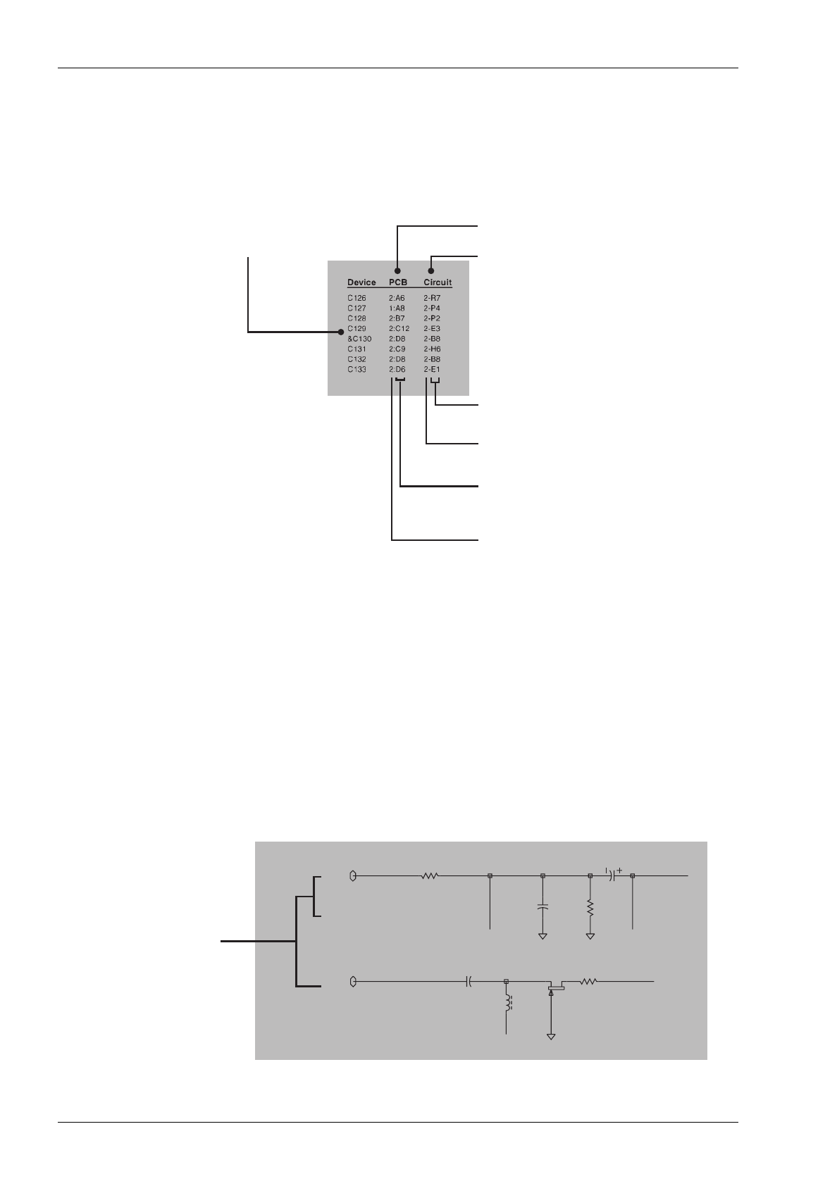
D5.1.6
T838/839 PCB Information
M830-00
30/04/98 Copyright TEL
Grid Reference Index
This section contains a component grid reference index to help you find components and labelled
pads on the PCB layouts and circuit diagrams. This index lists the components and pads in alpha-
numeric order, along with the appropriate alphanumeric grid references, as shown below:
Using CAD Circuit Diagrams
Reading a CAD circuit diagram is similar to reading a road map, in that both have an alphanumeric
border. The circuit diagrams in this manual use letters to represent the horizontal axis, and num-
bers for the vertical axis. These circuit diagram “grid references” are useful in following a circuit
that is spread over two or more sheets.
When a line representing part of the circuitry is discontinued, a reference will be given at the end of
the line to indicate where the rest of the circuitry is located, as shown below. The first digit refers to
the sheet number and the last two characters refer to the location on that sheet of the continuation of
the circuit (e.g. 1R3).
circuit diagram
reference
PCB layout
reference
components listed
in alphanumeric order
layer number -
1 = top side layer
2 = bottom side layer
component location
on the layer
sheet number
component location
on the sheet
C301
4N7
R303
12
D
S
G
L310
33U
IF-SIG
4R4
C369
100P
C371
10U
R339
100K
%R338
100
DISCRIMINATOR
1R3
2R9
2R9
8A2
t
hese grid references
s
how where the circuit
is continued

M830-00
T838 PCB Information
D5.2.1
Copyright TEL 30/04/98
5.2 T838 Power Amplifier PCB
This section contains the following information.
IPN Section Page
220-01404-03 Parts List
Mechanical & Miscellaneous Parts
Mechanical Assembly
Grid Reference Index
PCB Layout - Bottom Side
PCB Layout - Top Side
Control Section Circuit Diagram
RF & Thermistor Control Sections Circuit Diagram
5.2.3
5.2.6
5.2.7
5.2.9
5.2.11
5.2.12
5.2.13
5.2.14


IPN 220-01404-03
M830-00
T838 PCB Information
D5.2.3
Copyright TEL 23/07/99
T838 Parts List (IPN 220-01404-03)
How To Use This Parts List
The components listed in this parts list are divided into two main types: those with a circuit reference (e.g. C2, D1, R121, etc.) and
those without (miscellaneous and mechanical).
Those with a circuit reference are grouped in alphabetical order and then in numerical order within each group. Each component
entry comprises three or four columns: the circuit reference, variant (if applicable), IPN and description. A number in the variant col-
umn indicates that this is a variant component which is fitted only to the product type listed. Static sensitive devices are indicated by
an (S) at the start of the description column.
The miscellaneous and mechanical section lists the variant and common parts in IPN order. Where possible, a number in the legend
column indicates their position in the mechanical assembly drawing.
The Parts List Amendments box below lists component changes that took place after the parts list and diagrams in this section were
compiled. These changes (e.g. value changes, added/deleted components, etc.) are listed by circuit reference in alphanumeric order
and supersede the information given in the parts list or diagrams. Components without circuit references are listed in IPN order.
Parts List Amendments
D101, D105 Removed from the main PCB and replaced by two 1N4148 diodes (IPN 001-50012-00) placed on the D-range
PCB: one soldered between PL101 pins 5 and 7 (cathode), the other between PL101 pins 6 and 8 (cathode). To
allow external power meters to read zero and still provide meter overvoltage protection (710978).
D113 Changed from MR750 (IPN 001-00011-60) to MR2520L (IPN 001-00012-90) to provide overvoltage transient sup-
pression (750087/88/89/90/91/92).
IC204 Changed from LMC622CM to LM358 (710382).
R123, R158 Changed from 1k resistors (IPN 036-14100-00) to BA592 diodes (IPN 001-10059-20) to allow external power
meters to read zero (710978).
R207 Changed from 47k (IPN 036-15470-10) to 4k7 (IPN 036-14470-10)
R209 Changed from 1k5 (IPN 036-14150-10) to 390Ω (IPN 036-13390-10)
R210 Changed from 4k7 (IPN 036-14470-10) to 390Ω (IPN 036-13390-10)
R213 Changed from 3k9 (IPN 036-14390-00) to 560Ω (IPN 036-13560-00)
R218 Changed from 390Ω (IPN 036-13390-10) to 100Ω (IPN 036-13100-10)
R219 Changed from 100k NTC (IPN 045-06100-05) to 10k NTC (IPN 045-05100-02)
R220 Changed from 47k (IPN 036-15470-10) to 4k7 (IPN 036-14470-10)
R222 Changed from 47k (IPN 036-15470-10) to 4k7 (IPN 036-14470-10)
R224 Changed from 1k5 (IPN 036-14150-10) to 390Ω (IPN 036-13390-10)
R228 Changed from 4k7 (IPN 036-14470-10) to 390Ω (IPN 036-13390-10)
R229 Changed from 56k (IPN 036-15560-10) to 6k8 (IPN 036-14680-10)
349-00020-36 The two M3x8 Torx screws which secure the module into the rack frame have been replaced by M3x8 Pozidriv
screws (IPN 349-00020-55) (750101/2/3/5/6).
100k thermistor assembly
replaced with 10k item;
values of associated compo-
nents changed accordingly
(710394/411/447).

IPN 220-01404-03
D5.2.4
T838 PCB Information
M830-00
30/04/98 Copyright TEL
Ref Var IPN Description Ref Var IPN Description
C129 015-23680-08 CAP CER 0805 680P 10% X7R 50V
C131 015-27100-10 CAP CER 0805 1M+80-20% Y5V 16V
C132 015-24100-08 CAP CER 0805 1N 10% X7R 50V
C133 015-23680-08 CAP CER 0805 680P 10% X7R 50V
C137 015-23680-08 CAP CER 0805 680P 10% X7R 50V
C138 015-24470-08 CAP CER 0805 4N7 10% X7R 50V
C139 015-23680-08 CAP CER 0805 680P 10% X7R 50V
C141 014-07100-02 CAP TANT CHIP 1U0 3.2 X 1.6MM
C143 015-23680-08 CAP CER 0805 680P 10% X7R 50V
C145 015-23680-08 CAP CER 0805 680P 10% X7R 50V
C147 015-24470-08 CAP CER 0805 4N7 10% X7R 50V
C149 015-23680-08 CAP CER 0805 680P 10% X7R 50V
C151 015-23680-08 CAP CER 0805 680P 10% X7R 50V
C153 015-23680-08 CAP CER 0805 680P 10% X7R 50V
C155 015-25100-08 CAP CER 0805 10N 10% X7R 50V
C159 015-23680-08 CAP CER 0805 680P 10% X7R 50V
C161 015-23680-08 CAP CER 0805 680P 10% X7R 50V
C162 015-23680-08 CAP CER 0805 680P 10% X7R 50V
C164 015-24470-08 CAP CER 0805 4N7 10% X7R 50V
C165 015-23680-08 CAP CER 0805 680P 10% X7R 50V
C167 015-24100-08 CAP CER 0805 1N 10% X7R 50V
C169 014-07470-03 L) CAP TANT SMD 4U7 35V 20%
C171 015-24470-08 CAP CER 0805 4N7 10% X7R 50V
C173 015-23680-08 CAP CER 0805 680P 10% X7R 50V
C174 015-23680-08 CAP CER 0805 680P 10% X7R 50V
C176 015-06100-08 CAP CER 1206 100N 10% X7R 50V
C178 015-25100-08 CAP CER 0805 10N 10% X7R 50V
C179 015-06150-08 CAP CER1206150N10% X7R25VW 25V
C180 015-23680-08 CAP CER 0805 680P 10% X7R 50V
C181 015-23100-01 CAP CER 0805 100P 5% NPO 50V
C182 015-24470-08 CAP CER 0805 4N7 10% X7R 50V
C184 015-25100-08 CAP CER 0805 10N 10% X7R 50V
C185 015-23680-08 CAP CER 0805 680P 10% X7R 50V
C186 015-23680-08 CAP CER 0805 680P 10% X7R 50V
C187 015-06100-08 CAP CER 1206 100N 10% X7R 50V
C188 014-08100-00 CAP TANT CHIP 10M 16VW +-20%
C189 015-25100-08 CAP CER 0805 10N 10% X7R 50V
C190 015-23680-08 CAP CER 0805 680P 10% X7R 50V
C192 015-06100-08 CAP CER 1206 100N 10% X7R 50V
C193 015-06100-08 CAP CER 1206 100N 10% X7R 50V
C195 014-08100-00 CAP TANT CHIP 10M 16VW +-20%
C201 014-07470-03 L) CAP TANT SMD 4U7 35V 20%
*C203 015-03680-06 CAP CER 1210 680P NPO200VGRM42
*C204 015-03680-06 CAP CER 1210 680P NPO200VGRM42
C205 015-06100-08 CAP CER 1206 100N 10% X7R 50V
*C206 015-03680-06 CAP CER 1210 680P NPO200VGRM42
C207 015-06100-08 CAP CER 1206 100N 10% X7R 50V
C215 015-23680-08 CAP CER 0805 680P 10% X7R 50V
C216 015-24470-08 CAP CER 0805 4N7 10% X7R 50V
C218 015-23680-08 CAP CER 0805 680P 10% X7R 50V
C220 015-23680-08 CAP CER 0805 680P 10% X7R 50V
C221 015-06100-08 CAP CER 1206 100N 10% X7R 50V
C222 015-24470-08 CAP CER 0805 4N7 10% X7R 50V
C223 015-24100-08 CAP CER 0805 1N 10% X7R 50V
C224 015-23680-08 CAP CER 0805 680P 10% X7R 50V
C225 015-03680-06 CAP CER 1210 680P NPO200VGRM42
C226 015-23680-08 CAP CER 0805 680P 10% X7R 50V
C227 015-03680-06 CAP CER 1210 680P NPO200VGRM42
C229 015-03680-03 CAP CER 680P 5% NPO100V GRH111
C259 015-23680-08 CAP CER 0805 680P 10% X7R 50V
C261 015-24470-08 CAP CER 0805 4N7 10% X7R 50V
C268 029-02220-02 CAP MICA 5 CASE 22P 5%
C270 029-02560-03 CAP MICA 10 CASE 56P 2%
C271 029-02470-03 CAP MICA 10 CASE 47P 2%
C272 029-02560-03 CAP MICA 10 CASE 56P 2%
C273 029-02220-02 CAP MICA 5 CASE 22P 5%
C294 015-23680-08 CAP CER 0805 680P 10% X7R 50V
C295 015-24470-08 CAP CER 0805 4N7 10% X7R 50V
C297 015-23680-08 CAP CER 0805 680P 10% X7R 50V
C298 015-24470-08 CAP CER 0805 4N7 10% X7R 50V
D101 001-10000-70 (S) DIODE SMD BAV70 D-SW SOT23
D103 008-00013-32 (S) LED 3 RED LO CURRENT NO MTG
D105 001-10000-70 (S) DIODE SMD BAV70 D-SW SOT23
D107 008-00013-35 (S) LED 3 GRN LO CURRENT NO MTG
D109 008-00013-32 (S) LED 3 RED LO CURRENT NO MTG
D111 001-10000-70 (S) DIODE SMD BAV70 D-SW SOT23
D113 001-00011-60 (S) DIODE SR2607 -- USE MR750
D201 001-00013-45 (S) DIODE SCHTTKY 1SS97/2
D202 001-10000-70 (S) DIODE SMD BAV70 D-SW SOT23
D203 001-00013-45 (S) DIODE SCHTTKY 1SS97/2
IC101 002-10003-24 (S) IC SMD 324 4X O-AMP SO14
IC103 002-10003-24 (S) IC SMD 324 4X O-AMP SO14
IC105 002-10003-58 (S) IC SMD LM358 DUAL O-AMP
IC107 002-10003-17 (S) IC LM317L REG S0-8 100MA
IC109 002-10003-17 (S) IC LM317L REG S0-8 100MA
#IC201 10 004-00687-02 MODULE M68702L 135-160MHZ 60W
#IC201 20 004-00687-03 MODULE M68702H 150-174MHZ 60W
IC204 002-10006-62 (S)IC SMD LMC662CM 2X O-AMP
L101 065-10004-20 BEAD FE SMD CBD 4.6/3/3-4S2
L103 065-10004-20 BEAD FE SMD CBD 4.6/3/3-4S2
L105 065-10004-20 BEAD FE SMD CBD 4.6/3/3-4S2
*L201 056-10330-02 (L) IND SMD 330NH
L203 065-10004-20 BEAD FE SMD CBD 4.6/3/3-4S2
L206 056-14150-02 (L) IND SMD 1.5UH
L208 056-14150-02 (L) IND SMD 1.5UH
L215 052-08340-40 COIL A/W 4T/4.0MM SMD 0.8MM
L217 052-08340-40 COIL A/W 4T/4.0MM SMD 0.8MM
L233 056-10330-02 (L) IND SMD 330NH
L239 056-10330-02 (L) IND SMD 330NH
L241 052-08360-20 COIL A/W 2T/6.0MM SMD 0.8MM
L243 052-08340-20 COIL A/W 2T/4.0MM SMD 0.8MM
L245 052-08345-10 COIL A/W 1T/4.5MM SMD 0.8MM
L247 052-08340-20 COIL A/W 2T/4.0MM SMD 0.8MM
L248 052-08345-10 COIL A/W 1T/4.5MM SMD 0.8MM
L249 052-08360-20 COIL A/W 2T/6.0MM SMD 0.8MM
L264 056-10330-02 (L) IND SMD 330NH
LINK1 240-00020-68 HEADER 2W PCB MTG STD
LINK2 036-10000-00 RES M/F 0805 ZERO OHM
LINK201 240-00020-59 HEADER 3 W 1 R PCB MTG
PL101 240-00010-55 PLUG 15 W D RANGE W/W PNL MT
Q111 000-10008-57 (S) XSTR SMD BCW70 PNP SOT23 SS
Q113 000-10008-48 (S) XSTR SMD BCW60 NPN SOT23 SS
Q115 000-10008-57 (S) XSTR SMD BCW70 PNP SOT23 SS
Q117 000-10008-17 (S) XSTR SMD BC817-25 NPN SOT23
Q119 000-10008-48 (S) XSTR SMD BCW60 NPN SOT23 SS
Q121 000-10017-00 LS) XSTR SMD BF170LT1 SOT23
Q123 000-10008-57 (S) XSTR SMD BCW70 PNP SOT23 SS
Q125 000-10008-57 (S) XSTR SMD BCW70 PNP SOT23 SS
Q127 000-10008-57 (S) XSTR SMD BCW70 PNP SOT23 SS
Q129 000-10008-17 (S) XSTR SMD BC817-25 NPN SOT23
Q131 000-10017-00 LS) XSTR SMD BF170LT1 SOT23
Q133 000-10008-48 (S) XSTR SMD BCW60 NPN SOT23 SS
Q135 000-10008-17 (S) XSTR SMD BC817-25 NPN SOT23
Q136 000-10008-17 (S) XSTR SMD BC817-25 NPN SOT23
Q137 000-00030-95 (S) XSTR 2N6107 PNP TO220 AF
Q201 000-10008-48 (S) XSTR SMD BCW60 NPN SOT23 SS
R101 036-14100-00 RES M/F 0805 1K 5%
R103 036-15330-00 RES M/F 0805 33K 5%
R104 036-16470-00 RES M/F 0805 470K 5%
R117 036-16220-00 RES M/F 0805 220K 5%
R118 036-15270-00 RES M/F 0805 27K 5%
R119 036-16470-00 RES M/F 0805 470K 5%
R123 036-14100-00 RES M/F 0805 1K 5%
R124 036-16100-00 RES M/F 0805 100K 5%
R125 036-15100-00 RES M/F 0805 10K 5%
R126 036-14100-00 RES M/F 0805 1K 5%
R127 036-15100-00 RES M/F 0805 10K 5%
R128 036-15220-00 RES M/F 0805 22K 5%
R129 036-17100-00 RES M/F 0805 1M 5%
R130 036-14220-00 RES M/F 0805 2K2 5%
R131 036-16180-00 RES M/F 0805 180K 5%
R132 036-14100-00 RES M/F 0805 1K 5%
R133 036-15100-00 RES M/F 0805 10K 5%
R134 036-13470-00 RES M/F 0805 470E 5%
R135 036-13680-00 RES M/F 0805 680E 5%
R136 036-15100-00 RES M/F 0805 10K 5%
R137 036-13470-00 RES M/F 0805 470E 5%
R138 036-15100-00 RES M/F 0805 10K 5%
R141 036-15100-00 RES M/F 0805 10K 5%
R142 036-15100-00 RES M/F 0805 10K 5%
R143 036-15100-00 RES M/F 0805 10K 5%
R144 036-15820-00 RES M/F 0805 82K 5%
R145 036-15470-00 RES M/F 0805 47K 5%
R146 036-14180-00 RES M/F 0805 1K8 5%
R148 036-14820-00 RES M/F 0805 8K2 5%
R149 036-13470-00 RES M/F 0805 470E 5%
R150 036-12220-00 RES M/F 0805 22E 5%
R151 036-15100-00 RES M/F 0805 10K 5%
R152 036-15100-00 RES M/F 0805 10K 5%
R153 036-14680-00 RES M/F 0805 6K8 5%
R154 036-14680-00 RES M/F 0805 6K8 5%
R155 036-13220-00 RES M/F 0805 220E 5%
R156 036-13100-00 RES M/F 0805 100E 5%
Note: The T838 and T839 share the same basic design and
are built on the same PCB. While most components in
this design are common to both products, there are a
number of components that are placed in only one prod-
uct.
Because the circuit diagrams for this design cover both
products, we have indicated on the diagrams those
components which are placed only in the T838 by
enclosing them in a labelled box. The circuit reference
for each of these components is also prefixed with the
“*”character.
The “*” character is used in this parts list to indicate
components used only in the T838.

IPN 220-01404-03
M830-00
T838 PCB Information
D5.2.5
Copyright TEL 30/04/98
Ref Var IPN Description Ref Var IPN Description
R157 036-12220-00 RES M/F 0805 22E 5%
R158 036-14100-00 RES M/F 0805 1K 5%
R159 036-15100-00 RES M/F 0805 10K 5%
R160 036-14470-00 RES M/F 0805 4K7 5%
R161 036-14100-00 RES M/F 0805 1K 5%
R162 036-17100-00 RES M/F 0805 1M 5%
R163 036-13680-00 RES M/F 0805 680E 5%
R164 036-14220-00 RES M/F 0805 2K2 5%
R165 036-14100-00 RES M/F 0805 1K 5%
R166 036-13680-00 RES M/F 0805 680E 5%
R168 036-15100-10 RES M/F 0805 10K 1%
R169 036-14100-00 RES M/F 0805 1K 5%
R170 036-14100-00 RES M/F 0805 1K 5%
R171 036-14100-00 RES M/F 0805 1K 5%
R172 036-15100-10 RES M/F 0805 10K 1%
R173 036-13470-00 RES M/F 0805 470E 5%
R174 036-13220-00 RES M/F 0805 220E 5%
R175 036-16220-00 RES M/F 0805 220K 5%
R176 036-15100-00 RES M/F 0805 10K 5%
R177 036-14470-00 RES M/F 0805 4K7 5%
R178 036-16100-00 RES M/F 0805 100K 5%
R179 036-15100-00 RES M/F 0805 10K 5%
R180 036-16150-00 RES M/F 0805 150K 5%
R181 036-14560-00 RES M/F 0805 5K6 5%
R182 036-16100-00 RES M/F 0805 100K 5%
R183 036-14470-00 RES M/F 0805 4K7 5%
R184 036-14100-00 RES M/F 0805 1K 5%
R185 036-03100-02 RES 100E 1206 200V 250MW RC01
R186 036-13100-00 RES M/F 0805 100E 5%
R187 036-03150-03 RES 1218 PWR CHIP 150E 20% 1W
R188 036-13220-00 RES M/F 0805 220E 5%
R189 036-12100-00 RES M/F 0805 10E 5%
R190 036-12220-00 RES M/F 0805 22E 5%
R191 036-14100-10 RES M/F 0805 CHIP 1K 1%
R192 036-13220-10 RES 0805 220E 1%
R193 036-12100-00 RES M/F 0805 10E 5%
R194 036-03220-03 RES 1218 PWR CHIP 220E 20% 1W
R195 036-14220-00 RES M/F 0805 2K2 5%
R196 036-13100-00 RES M/F 0805 100E 5%
R197 036-10000-00 RES M/F 0805 ZERO OHM
*R201 036-03330-03 L) RES 1218 PWR 330E 20% 1W
*R202 036-02100-03 L) RES 1218 PWR 10E 20% 1W
R203 036-02100-02 RES 10E 1206 200V 250MW RC01
*R204 036-03330-03 L) RES 1218 PWR 330E 20% 1W
R205 036-02100-02 RES 10E 1206 200V 250MW RC01
R207 036-15470-10 RES M/F 0805 47K 1%
R209 036-14150-10 RES MF 0805 CHIP 1K5 1%
R210 036-14470-10 RES M/F 0805 CHIP 4K7 1%
R212 036-15100-00 RES M/F 0805 10K 5%
R213 036-14390-00 RES M/F 0805 3K9 5%
R214 036-14470-00 RES M/F 0805 4K7 5%
R218 036-13390-10 RES MF 0805 CHIP 390E 1%
R219 available as sub-assembly only - refer to
(045-06100-05) in the mechanical parts list
R220 036-15470-10 RES M/F 0805 47K 1%
R222 036-15470-10 RES M/F 0805 47K 1%
R224 036-14150-10 RES MF 0805 CHIP 1K5 1%
R225 030-03120-00 RES FILM 120E 5% 0.25W 7X2.5
R228 036-14470-10 RES M/F 0805 CHIP 4K7 1%
R229 036-15560-10 RES MF 0805 CHIP 56K 1%
R231 030-03120-00 RES FILM 120E 5% 0.25W 7X2.5
R237 045-04470-00 RES NTC SMD 4K7 5% 20MW
RV101 042-04500-05 RES PRESET SMD 5K CER 4MM SQ
RV103 042-05500-05 RES PRESET SMD 50K CER 4MM SQ
RV105 042-04500-05 RES PRESET SMD 5K CER 4MM SQ
RV107 042-05500-05 RES PRESET SMD 50K CER 4MM SQ
RV109 044-04200-03 RES PRE 2K 10 TURN PNL MTG
RV113 042-06500-05 RES PRESET SMD 500K CER 4MM SQ
RV115 042-04220-05 RES PRESET SMD 2K CER 4MM SQ
SK101 240-10000-05 CONN SMD SKT 8W 2R M-MATCH
SK103 240-10000-05 CONN SMD SKT 8W 2R M-MATCH
*SK203 240-02100-44 SKT COAX MINI JACK PCB MT ANG.
16

IPN 220-01404-03
D5.2.6
T838 PCB Information
M830-00
30/04/98 Copyright TEL
IPN Legend Description IPN Legend Description
T838 Mechanical & Miscellaneous Parts (220-01404-03)
000-00030-95 9 Q137
004-00687-02/3 14 #IC201
012-04150-01 22 CAP CER F/THRU 1N5 NO LEAD
045-06100-05 16 ASSY 100K NTC FOR MODULE
R219
051-00006-02 SOLDER SPRING 1.3MM A4M1877
Support for front panel LED solder joints.
051-00641-01 3 COAX SEMI-RIG N-TYPE EXTN
051-00642-01 28 COAX SEMI-RIG N-TYPE EXTN
065-00010-13 21 BEAD FER 7D 1.9X0.9X3.8
201-00030-02 WIRE T/C 7/0.2 PVC RED
Front panel LEDs.
201-00030-10 WIRE T/C 7/0.2 PVC BLACK
Front panel LEDs.
201-00050-25 AUTO 154 RED 41/0.3 PVC
DC+ from D-range PCB.
201-00050-26 AUTO 154 BLACK 41/0.3 PVC
DC- from D-range PCB.
206-00010-11 COAX 50 OHM RG316-U PTFE
Coax from BNC connector to *SK203.
219-02591-00 18 LOOM RIBBON 8 WAY FOR PA
219-02592-00 CABLE ASSY RG223/U N TO BNC
Exciter/PA connecting cable.
220-01402-02 2 PCB T838/9 TEFLON DIRNL COUPLER
220-01404-03 1 PCB T838/9 PA MODULE DESIGN
240-00010-55 20 PLUG 15 W D RANGE W/W PNL MT
PL101
240-00100-43 PLG COAX MINI PIN CRIMP 1.5D
Coax from BNC connector to *SK203.
240-02010-54 SKT 15W DRANGE PNL MTG 125 C
Matching socket for D-range plug PL101.
240-02100-06 27 SKT COAX N TYPE PNL MTG OP-TER
240-02100-17 29 SKT COAX BNC PNL JAC CRP RG316
240-04020-62 SKT 2 W RECEP SHORTING LINK
LINK1
240-06010-14 CLAMP LATCHING 15 W D RANGE
Cover for D-range socket.
240-06010-15 25 BLOCK LATCHING 15W D RANGE
240-06010-44 26 HOOD CONN UHF & N-TYPE
303-23120-00 30 COVER A3M2288 HOLE BLANKING
303-23146-00 38 COVER SIDE T838/9PA
308-01007-01 35 HANDLE BASE STATION SERIES II
308-13122-02 6 HEATSINK T838/9 PA COMPLETE
316-06617-00 32 PNL PA NO INP DRV SER II SNGL
319-01152-00 19 SHIELD A3M2250 F/THRU MTG
319-01190-01 4 SHIELD WALL HARM. FILTER
319-01201-00 31 SHIELD LID HARM. FILTER
319-01202-00 5 SHIELD PA CONTROL CIRCUIT
319-30064-00 13 SPACER HSINK RF MODULE
345-00040-16 23 SCRW M3X20MM P/POZ ST BZ
349-00010-59 17 SCRW 6-32 X 3/8 P/PH T/T ZP
349-00020-07 7 SCRW 4-40 X 5/16 P/POZ T/T BLK
349-00020-09 12 SCRW T/T 4-40X3/8 IN P/POZ BLK
349-00020-36 37 LIM)SCREW TT M3X8m PANTORX BLK
352-00010-29 36 NUT M4 NYLOC HEX
353-00010-10 11 WSHR M3 FLAT 7MMX0.6MM ST BZ
356-00010-03 24 TAG SOLDER 3MM LONG M614/3.2
356-00010-05 15 TAG SOLDER 4MM LONG M6144/4.2
360-00010-41 34 BUSH SHORTY BLK
362-00010-07 8 GASKET SIL INSULATING TO-220
362-00010-13 10 BUSH INSULATING 1.1MM TOP HAT
362-00010-33 33 GROMMET LED MTG 3MM
365-00100-20 LABEL WHITE S/A 28X11MM
365-01391-01 LABEL 30X10.8 T/MARK VOID
365-01538-00 LABEL WARNING 60W/PWR CLAMP
369-00010-14 TIE CABLE NYLON 100X2.6MM
399-00010-56 BAG PLASTIC 200X250MM
400-00020-07 SLEEVING 2MM SIL RUBBER
410-00010-43 PKG T296 AMPAC REF 73-46


IPN 220-01404-03
M830-00
T838 PCB Information
D5.2.9
Copyright TEL 30/04/98
Device PCB Circuit Device PCB CircuitDevice PCB Circuit Device PCB Circuit
T838 Grid Reference Index (IPN 220-01404-03)
How To Use This Grid Reference Index
The first digit in the PCB layout reference is a "1" or "2", indicating the top or bottom side layout respectively, and the last two charac-
ters give the location of the component on that diagram.
The first digit in the circuit diagram reference is the sheet number, and the last two characters give the location of the component on
that sheet.
*C101 1:E4 1-B8
*C103 1:E4 1-B9
*C105 1:B3 1-D8
*C107 1:B3 1-D9
*C109 1:B3 1-D8
*C111 1:C4 1-D8
*C113 1:B5 1-F8
*C115 1:B5 1-F8
*C117 1:B5 1-F9
*C119 1:B5 1-G8
*C121 1:D4 1-B6
*C123 1:D4 1-B6
*C124 1:E3 1-C6
*C125 1:C4 1-D7
*C127 1:C4 1-D6
C129 1:B3 1-H5
C131 1:B3 1-J6
C132 1:A3 1-K7
C133 1:B4 1-K8
C137 1:B2 1-K8
C138 1:B2 1-L8
C139 1:B4 1-M6
C141 1:B3 1-M8
C143 1:E3 1-E7
C145 1:E3 1-F7
C147 1:D3 1-F6
C149 1:D3 1-F7
C151 1:C5 1-D5
C153 1:B5 1-D3
C155 1:D3 1-G3
C159 1:B3 1-H2
C161 1:B4 1-K4
C162 1:B3 1-L4
C164 1:B3 1-L4
C165 1:B3 1-M4
C167 1:K3 1-P3
C169 1:K3 1-P3
C171 1:K3 1-Q3
C173 1:D4 1-B0
C174 1:E4 1-B0
C176 1:D4 1-E0
C178 1:C4 1-F0
C179 1:D3 1-G2
C180 1:E2 1-H0
C181 1:D3 1-G0
C182 1:D3 1-H1
C184 1:D4 1-G0
C185 1:D2 1-J1
C186 1:E2 1-J0
C187 1:D3 1-K1
C188 1:C2 1-L1
C189 1:C3 1-M1
C190 1:C3 1-N1
C192 1:B2 1-N1
C193 1:B2 1-P1
C195 1:C2 1-Q1
C201 1:J7 2-L5
*C202 1:H3 2-B8
*C203 1:P7 2-C1
*C204 1:M6 2-E1
C205 1:L7 2-I5
*C206 1:P6 2-C1
C207 1:K7 2-K5
*C208 1:H3 2-C8
*C209 1:C5 2-D8
*C210 1:C5 2-E8
*C212 1:D5 2-G9
*C213 1:D4 2-H9
C215 1:D5 2-J8
C216 1:H6 2-B6
*C217 1:P3 2-E3
C218 1:H5 2-C6
*C219 1:P2 2-E3
C220 1:E5 2-D6
C221 1:E5 2-N8
C222 1:E5 2-E6
C223 1:D5 2-G7
C224 1:D5 2-M8
C225 1:L6 2-I4
C226 1:D4 2-H7
C227 1:K6 2-J4
C229 1:H6 2-K4
*C230 1:L4 2-I2
*C231 1:L4 2-I1
*C232 1:K4 2-J1
*C233 1:K4 2-K2
*C234 1:J4 2-L1
*C240 1:H4 2-K1
C259 1:F7 2-Q3
C261 1:F6 2-Q4
C268 1:E6 2-S2
C270 1:D6 2-T2
C271 1:C6 2-T2
C272 1:B6 2-U2
C273 1:B6 2-V2
C294 1:D6 2-R1
C295 1:D6 2-R1
C297 1:C5 2-L8
C298 1:C6 2-L8
D101 1:B3 1-H5
D101 1:B3 1-G5
D103 1:P7 1-K9
D105 1:C2 1-J2
D105 1:C2 1-J2
D107 1:P7 1-K5
D109 1:P6 1-L5
D111 1:C2 1-M1
D111 1:C2 1-M1
D113 1:F7 1-Q2
D201 1:F6 2-Q3
D202 1:D4 2-I8
D202 1:D4 2-I8
D203 1:E6 2-R2
IC101 1:D4 1-C6
IC101 1:D4 1-G0
IC101 1:D4 1-B8
IC101 1:D4 1-C0
IC101 1:D4 1-N0
IC103 1:C4 1-D4
IC103 1:C4 1-J8
IC103 1:C4 1-F0
IC103 1:C4 1-J5
IC103 1:C4 1-E3
IC105 1:D3 1-M0
IC105 1:D3 1-P0
IC105 1:D3 1-G2
IC107 1:D3 1-K1
IC109 1:B2 1-N1
#IC201 1:K7 2-I4
*#IC202 1:K4 2-I1
*IC203 1:N5 2-F2
IC204 1:D5 2-H7
IC204 1:D5 2-H8
IC204 1:D5 2-N8
*IC205 1:G5 2-P2
L101 1:K3 1-P3
L103 1:K2 1-Q3
L105 1:E2 1-K0
*L201 1:P7 2-C1
*L202 1:H3 2-B8
L203 1:L7 2-I6
*L204 1:C5 2-D8
L206 1:H5 2-B7
L208 1:E5 2-D7
*L211 1:P2 2-D3
L215 1:L7 2-I5
L217 1:J7 2-K5
*L223 1:J4 2-K2
*L230 1:L4 2-I3
*L231 1:L4 2-I2
L233 1:F6 2-Q3
*L236 1:H6 2-M2
L239 1:E5 2-R2
L241 1:D6 2-S3
L243 1:C6 2-T3
L245 1:C7 2-T2
L247 1:C6 2-U3
L248 1:D7 2-U2
L249 1:B6 2-V3
L264 1:C6 2-L8
LINK1 1:D3 1-L0
LINK2 1:P6 1-D1
LINK201 1:D5 2-F8
P101 1:A5 1-R9
P103 1:K3 1-R0
P105 1:K2 1-R0
P201 1:B6 2-V3
PL101 1:L3 1-C2
*Q101 1:C3 1-C9
*Q103 1:B3 1-E8
*Q105 1:C4 1-D7
*Q107 1:B5 1-F8
*Q109 1:A5 1-G9
Q111 1:A3 1-J7
Q113 1:A3 1-K6
Q115 1:A3 1-L7
Q117 1:B4 1-K8
Q119 1:B4 1-L6
Q121 1:B3 1-L8
Q123 1:E3 1-E7
Q125 1:E3 1-F7
Q127 1:D3 1-G7
Q129 1:B4 1-L4
Q131 1:B3 1-M5
Q133 1:D4 1-D0
Q135 1:E2 1-H0
Q136 1:E3 1-H0
Q137 1:D2 1-J0
Q201 1:D5 2-K8
R101 1:E4 1-A8
*R102 1:E4 1-A9
R103 1:E4 1-A8
R104 1:E4 1-B9
*R105 1:D4 1-C8
*R106 1:B3 1-C8
*R107 1:C4 1-D7
*R108 1:B3 1-E9
*R109 1:C3 1-E9
*R111 1:B5 1-E8
*R112 1:B5 1-E9
*R113 1:B5 1-F9
*R114 1:C4 1-A6
*R115 1:C5 1-A6
*R116 1:D4 1-A7
R117 1:C4 1-A6
R118 1:D4 1-B6
R119 1:D4 1-C7
*R120 1:E3 1-H7
*R121 1:C4 1-C7
*R122 1:C4 1-D6
R123 1:B4 1-H7
R124 1:B4 1-H8
R125 1:B4 1-H8
R126 1:B3 1-H6
R127 1:A3 1-H7
R128 1:A3 1-J7
R129 1:B4 1-J9
R130 1:B4 1-J8
R131 1:A3 1-J7
R132 1:B5 1-J8
R133 1:A3 1-K7
R134 1:B3 1-K6
R135 1:P7 1-K9
R136 1:A3 1-K7
R137 1:B3 1-K6
R138 1:B4 1-L6
Note:
This grid reference index
covers both the T838 and
T839 and is reproduced in
both PCB Information sec-
tions for your convenience.

IPN 220-01404-03
D5.2.10
T838 PCB Information
M830-00
30/04/98 Copyright TEL
Device PCB Circuit Device PCB CircuitDevice PCB Circuit Device PCB Circuit
R141 1:E3 1-C6
R142 1:E3 1-E7
R143 1:E4 1-F6
R144 1:D3 1-F6
R145 1:E4 1-F7
R146 1:E4 1-G7
R148 1:C5 1-D5
R149 1:C5 1-C4
R150 1:C4 1-F0
R151 1:B5 1-D5
R152 1:B5 1-C3
R153 1:C5 1-F4
R154 1:C5 1-F3
R155 1:D3 1-F2
R156 1:D3 1-F3
R157 1:D4 1-G0
R158 1:C4 1-H3
R159 1:C4 1-H4
R160 1:C3 1-J5
R161 1:B3 1-J3
R162 1:B3 1-K4
R163 1:P8 1-K5
R164 1:B3 1-K4
R165 1:B4 1-K4
R166 1:P7 1-L5
R168 1:E4 1-A1
R169 1:E4 1-A0
R170 1:D4 1-B0
R171 1:E4 1-B0
R172 1:E4 1-B0
R173 1:P6 1-C1
R174 1:P6 1-C1
R175 1:D4 1-C0
R176 1:D4 1-D0
R177 1:D4 1-D0
R178 1:D3 1-E1
R179 1:D4 1-E0
R180 1:D4 1-E0
R181 1:E3 1-F2
R182 1:D4 1-E0
R183 1:D4 1-F1
R184 1:E3 1-G1
R185 1:E2 1-J0
R186 1:D2 1-H1
R187 1:E2 1-H0
R188 1:D2 1-L1
R189 1:D2 1-L1
R190 1:C3 1-M1
R191 1:B2 1-P1
R192 1:B2 1-P1
R193 1:C2 1-Q1
R194 1:D2 1-H0
R195 1:D3 1-J0
R196 1:D3 1-J0
R197 1:D3 1-L1
*R201 1:N6 2-D1
*R202 1:N6 2-D1
R203 1:L7 2-I5
*R204 1:N6 2-D1
R205 1:K7 2-K4
*R206 1:C5 2-E8
R207 1:D4 2-F8
*R208 1:C5 2-G9
R209 1:D5 2-G8
R210 1:D5 2-G8
*R211 1:D4 2-H9
R212 1:D4 2-I8
R213 1:D5 2-E7
R214 1:E4 2-J8
*R215 1:H3 2-B8
*R216 1:P6 2-E2
*R217 1:P6 2-E2
R218 1:E5 2-E7
R219 1:H6 2-B6
R220 1:E5 2-F7
R222 1:D5 2-G7
*R223 1:F2 2-P2
R224 1:D4 2-G7
R225 1:E6 2-R3
R228 1:E4 2-G7
R229 1:D4 2-H7
*R2301:L42-I2
R231 1:F5 2-Q2
*R232 1:K4 2-K1
R237 1:C5 2-K8
RV101 1:C4 1-H8
RV103 1:C4 1-H6
RV105 1:C3 1-J5
RV107 1:C3 1-J3
RV109 1:P5 1-C2
*RV111 1:P5 1-D1
RV113 1:C3 1-D0
RV115 1:C3 1-K0
SK101 1:K3 1-A2
SK103 1:B4 1-B2
*SK201 1:N3 2-D3
*SK203 1:N7 2-C1

M830-00
T839 PCB Information
D5.3.1
Copyright TEL 30/04/98
5.3 T839 Power Amplifier PCB
This section contains the following information.
IPN Section Page
220-01404-03 Parts List
Mechanical & Miscellaneous Parts
Mechanical Assembly
Grid Reference Index
PCB Layout - Bottom Side
PCB Layout - Top Side
Control Section Circuit Diagram
RF & Thermistor Control Sections Circuit Diagram
5.3.3
5.3.6
5.3.7
5.3.9
5.3.11
5.3.12
5.3.13
5.3.14


IPN 220-01404-03
M830-00
T839 PCB Information
D5.3.3
Copyright TEL 23/07/99
T839 Parts List (IPN 220-01404-03)
How To Use This Parts List
The components listed in this parts list are divided into two main types: those with a circuit reference (e.g. C2, D1, R121, etc.) and
those without (miscellaneous and mechanical).
Those with a circuit reference are grouped in alphabetical order and then in numerical order within each group. Each component
entry comprises three or four columns: the circuit reference, variant (if applicable), IPN and description. A number in the variant col-
umn indicates that this is a variant component which is fitted only to the product type listed. Static sensitive devices are indicated by
an (S) at the start of the description column.
The miscellaneous and mechanical section lists the variant and common parts in IPN order. Where possible, a number in the legend
column indicates their position in the mechanical assembly drawing.
The Parts List Amendments box below lists component changes that took place after the parts list and diagrams in this section were
compiled. These changes (e.g. value changes, added/deleted components, etc.) are listed by circuit reference in alphanumeric order
and supersede the information given in the parts list or diagrams. Components without circuit references are listed in IPN order.
Parts List Amendments
D101, D105 Removed from the main PCB and replaced by two 1N4148 diodes (IPN 001-50012-00) placed on the D-range
PCB: one soldered between PL101 pins 5 and 7 (cathode), the other between PL101 pins 6 and 8 (cathode). To
allow external power meters to read zero and still provide meter overvoltage protection (710978).
D113 Changed from MR750 (IPN 001-00011-60) to MR2520L (IPN 001-00012-90) to provide overvoltage transient sup-
pression (750087/88/89/90/91/92).
IC204 Changed from LMC622CM to LM358 (710382).
*L236 Changed from through-hole link (IPN 051-00640-01) to SMD link (IPN 051-00640-02) (710580).
R123, R158 Changed from 1k resistors (IPN 036-14100-00) to BA592 diodes (IPN 001-10059-20) to allow external power
meters to read zero (710978).
*R206 Changed from 390Ω (IPN 036-13390-10) to 100Ω (IPN 036-13100-10)
R207, *R208 Changed from 47k (IPN 036-15470-10) to 4k7 (IPN 036-14470-10)
R209 Changed from 1k5 (IPN 036-14150-10) to 390Ω (IPN 036-13390-10)
R210 Changed from 4k7 (IPN 036-14470-10) to 390Ω (IPN 036-13390-10)
*R211 Changed from 56k (IPN 036-15560-10) to 6k8 (IPN 036-14680-10)
R213 Changed from 3k9 (IPN 036-14390-00) to 560Ω (IPN 036-13560-00)
*R215 Changed from 100k NTC (IPN 045-06100-05) to 10k NTC (IPN 045-05100-02)
R218 Changed from 390Ω (IPN 036-13390-10) to 100Ω (IPN 036-13100-10)
R219 Changed from 100k NTC (IPN 045-06100-05) to 10k NTC (IPN 045-05100-02)
R220, R222 Changed from 47k (IPN 036-15470-10) to 4k7 (IPN 036-14470-10)
R224 Changed from 1k5 (IPN 036-14150-10) to 390Ω (IPN 036-13390-10)
R228 Changed from 4k7 (IPN 036-14470-10) to 390Ω (IPN 036-13390-10)
R229 Changed from 56k (IPN 036-15560-10) to 6k8 (IPN 036-14680-10)
258-00010-03 Cooling fan: some T839 PAs may be fitted with a different fan (IPN 258-00010-06). If so, a 100µH inductor (IPN
056-00021-02) may be fitted in series in the fan power feed wire with a 10µF capacitor (IPN 025-08100-03) fitted
in parallel with this inductor (710977).
349-00020-36 The two M3x8 Torx screws which secure the module into the rack frame have been replaced by M3x8 Pozidriv
screws (IPN 349-00020-55) (750101/2/3/5/6).
100k thermistor assembly
replaced with 10k item;
values of associated compo-
nents changed accordingly
(710394/411/447).

IPN 220-01404-03
D5.3.4
T839 PCB Information
M830-00
30/04/98 Copyright TEL
Ref Var IPN Description Ref Var IPN Description
*C101 015-23680-08 CAP CER 0805 680P 10% X7R 50V
*C103 015-23680-08 CAP CER 0805 680P 10% X7R 50V
*C105 015-23680-08 CAP CER 0805 680P 10% X7R 50V
*C107 015-23680-08 CAP CER 0805 680P 10% X7R 50V
*C109 015-23680-08 CAP CER 0805 680P 10% X7R 50V
*C111 015-23680-08 CAP CER 0805 680P 10% X7R 50V
*C113 015-23680-08 CAP CER 0805 680P 10% X7R 50V
*C115 015-23680-08 CAP CER 0805 680P 10% X7R 50V
*C117 015-23680-08 CAP CER 0805 680P 10% X7R 50V
*C119 015-23680-08 CAP CER 0805 680P 10% X7R 50V
*C121 015-23680-08 CAP CER 0805 680P 10% X7R 50V
*C123 015-23680-08 CAP CER 0805 680P 10% X7R 50V
*C124 015-23680-08 CAP CER 0805 680P 10% X7R 50V
*C125 015-23680-08 CAP CER 0805 680P 10% X7R 50V
*C127 015-23680-08 CAP CER 0805 680P 10% X7R 50V
C129 015-23680-08 CAP CER 0805 680P 10% X7R 50V
C131 015-27100-10 CAP CER 0805 1M+80-20% Y5V 16V
C132 015-24100-08 CAP CER 0805 1N 10% X7R 50V
C133 015-23680-08 CAP CER 0805 680P 10% X7R 50V
C137 015-23680-08 CAP CER 0805 680P 10% X7R 50V
C138 015-24470-08 CAP CER 0805 4N7 10% X7R 50V
C139 015-23680-08 CAP CER 0805 680P 10% X7R 50V
C141 014-07100-02 CAP TANT CHIP 1U0 3.2 X 1.6MM
C143 015-23680-08 CAP CER 0805 680P 10% X7R 50V
C145 015-23680-08 CAP CER 0805 680P 10% X7R 50V
C147 015-24470-08 CAP CER 0805 4N7 10% X7R 50V
C149 015-23680-08 CAP CER 0805 680P 10% X7R 50V
C151 015-23680-08 CAP CER 0805 680P 10% X7R 50V
C153 015-23680-08 CAP CER 0805 680P 10% X7R 50V
C155 015-25100-08 CAP CER 0805 10N 10% X7R 50V
C159 015-23680-08 CAP CER 0805 680P 10% X7R 50V
C161 015-23680-08 CAP CER 0805 680P 10% X7R 50V
C162 015-23680-08 CAP CER 0805 680P 10% X7R 50V
C164 015-24470-08 CAP CER 0805 4N7 10% X7R 50V
C165 015-23680-08 CAP CER 0805 680P 10% X7R 50V
C167 015-24100-08 CAP CER 0805 1N 10% X7R 50V
C169 014-07470-03 L) CAP TANT SMD 4U7 35V 20%
C171 015-24470-08 CAP CER 0805 4N7 10% X7R 50V
C173 015-23680-08 CAP CER 0805 680P 10% X7R 50V
C174 015-23680-08 CAP CER 0805 680P 10% X7R 50V
C176 015-06100-08 CAP CER 1206 100N 10% X7R 50V
C178 015-25100-08 CAP CER 0805 10N 10% X7R 50V
C179 015-06150-08 CAP CER1206150N10% X7R25VW 25V
C180 015-23680-08 CAP CER 0805 680P 10% X7R 50V
C181 015-23100-01 CAP CER 0805 100P 5% NPO 50V
C182 015-24470-08 CAP CER 0805 4N7 10% X7R 50V
C184 015-25100-08 CAP CER 0805 10N 10% X7R 50V
C185 015-23680-08 CAP CER 0805 680P 10% X7R 50V
C186 015-23680-08 CAP CER 0805 680P 10% X7R 50V
C187 015-06100-08 CAP CER 1206 100N 10% X7R 50V
C188 014-08100-00 CAP TANT CHIP 10M 16VW +-20%
C189 015-25100-08 CAP CER 0805 10N 10% X7R 50V
C190 015-23680-08 CAP CER 0805 680P 10% X7R 50V
C192 015-06100-08 CAP CER 1206 100N 10% X7R 50V
C193 015-06100-08 CAP CER 1206 100N 10% X7R 50V
C195 014-08100-00 CAP TANT CHIP 10M 16VW +-20%
C201 014-07470-03 L) CAP TANT SMD 4U7 35V 20%
*C202 015-24470-08 CAP CER 0805 4N7 10% X7R 50V
C205 015-06100-08 CAP CER 1206 100N 10% X7R 50V
C207 015-06100-08 CAP CER 1206 100N 10% X7R 50V
*C208 015-23680-08 CAP CER 0805 680P 10% X7R 50V
*C209 015-23680-08 CAP CER 0805 680P 10% X7R 50V
*C210 015-24470-08 CAP CER 0805 4N7 10% X7R 50V
*C212 015-24100-08 CAP CER 0805 1N 10% X7R 50V
*C213 015-23680-08 CAP CER 0805 680P 10% X7R 50V
C215 015-23680-08 CAP CER 0805 680P 10% X7R 50V
C216 015-24470-08 CAP CER 0805 4N7 10% X7R 50V
*C217 015-03680-06 CAP CER 1210 680P NPO200VGRM42
C218 015-23680-08 CAP CER 0805 680P 10% X7R 50V
*C219 015-03680-06 CAP CER 1210 680P NPO200VGRM42
C220 015-23680-08 CAP CER 0805 680P 10% X7R 50V
C221 015-06100-08 CAP CER 1206 100N 10% X7R 50V
C222 015-24470-08 CAP CER 0805 4N7 10% X7R 50V
C223 015-24100-08 CAP CER 0805 1N 10% X7R 50V
C224 015-23680-08 CAP CER 0805 680P 10% X7R 50V
C225 015-03680-06 CAP CER 1210 680P NPO200VGRM42
C226 015-23680-08 CAP CER 0805 680P 10% X7R 50V
C227 015-03680-06 CAP CER 1210 680P NPO200VGRM42
C229 015-03680-03 CAP CER 680P 5% NPO100V GRH111
*C230 015-06100-08 CAP CER 1206 100N 10% X7R 50V
*C231 015-03680-06 CAP CER 1210 680P NPO200VGRM42
*C232 015-03680-06 CAP CER 1210 680P NPO200VGRM42
*C233 015-06100-08 CAP CER 1206 100N 10% X7R 50V
*C234 014-07470-03 L) CAP TANT SMD 4U7 35V 20%
*C240 015-03680-03 CAP CER 680P 5% NPO100V GRH111
C259 015-23680-08 CAP CER 0805 680P 10% X7R 50V
C261 015-24470-08 CAP CER 0805 4N7 10% X7R 50V
C268 029-02220-02 CAP MICA 5 CASE 22P 5%
C270 029-02560-03 CAP MICA 10 CASE 56P 2%
C271 029-02470-03 CAP MICA 10 CASE 47P 2%
C272 029-02560-03 CAP MICA 10 CASE 56P 2%
C273 029-02220-02 CAP MICA 5 CASE 22P 5%
C294 015-23680-08 CAP CER 0805 680P 10% X7R 50V
C295 015-24470-08 CAP CER 0805 4N7 10% X7R 50V
C297 015-23680-08 CAP CER 0805 680P 10% X7R 50V
C298 015-24470-08 CAP CER 0805 4N7 10% X7R 50V
D101 001-10000-70 (S) DIODE SMD BAV70 D-SW SOT23
D103 008-00013-32 (S) LED 3 RED LO CURRENT NO MTG
D105 001-10000-70 (S) DIODE SMD BAV70 D-SW SOT23
D107 008-00013-35 (S) LED 3 GRN LO CURRENT NO MTG
D109 008-00013-32 (S) LED 3 RED LO CURRENT NO MTG
D111 001-10000-70 (S) DIODE SMD BAV70 D-SW SOT23
D113 001-00011-60 (S) DIODE SR2607 -- USE MR750
D201 001-00013-45 (S) DIODE SCHTTKY 1SS97/2
D202 001-10000-70 (S) DIODE SMD BAV70 D-SW SOT23
D203 001-00013-45 (S) DIODE SCHTTKY 1SS97/2
IC101 002-10003-24 (S) IC SMD 324 4X O-AMP SO14
IC103 002-10003-24 (S) IC SMD 324 4X O-AMP SO14
IC105 002-10003-58 (S) IC SMD LM358 DUAL O-AMP
IC107 002-10003-17 (S) IC LM317L REG S0-8 100MA
IC109 002-10003-17 (S) IC LM317L REG S0-8 100MA
#IC201 10 004-00687-02 MODULE M68702L 135-160MHZ 60W
#IC201 20 004-00687-03 MODULE M68702H 150-174MHZ 60W
*#IC202 10 004-00687-02 MODULE M68702L 135-160MHZ 60W
*#IC202 20 004-00687-03 MODULE M68702H 150-174MHZ 60W
*IC203 051-00005-36 RFPOWER 3DB HYBRID COUPLER
IC204 002-10006-62 (S)IC SMD LMC662CM 2X O-AMP
*IC205 051-00005-36 RFPOWER 3DB HYBRID COUPLER
L101 065-10004-20 BEAD FE SMD CBD 4.6/3/3-4S2
L103 065-10004-20 BEAD FE SMD CBD 4.6/3/3-4S2
L105 065-10004-20 BEAD FE SMD CBD 4.6/3/3-4S2
*L202 056-14150-02 (L) IND SMD 1.5UH
L203 065-10004-20 BEAD FE SMD CBD 4.6/3/3-4S2
*L204 056-14150-02 (L) IND SMD 1.5UH
L206 056-14150-02 (L) IND SMD 1.5UH
L208 056-14150-02 (L) IND SMD 1.5UH
*L211 056-10330-02 (L) IND SMD 330NH
L215 052-08340-40 COIL A/W 4T/4.0MM SMD 0.8MM
L217 052-08340-40 COIL A/W 4T/4.0MM SMD 0.8MM
*L223 052-08340-40 COIL A/W 4T/4.0MM SMD 0.8MM
*L230 065-10004-20 BEAD FE SMD CBD 4.6/3/3-4S2
*L231 052-08340-40 COIL A/W 4T/4.0MM SMD 0.8MM
L233 056-10330-02 (L) IND SMD 330NH
*L236 051-00640-01 LNK 65.5 COP STPL C/W SLCN SLV
L239 056-10330-02 (L) IND SMD 330NH
L241 052-08360-20 COIL A/W 2T/6.0MM SMD 0.8MM
L243 052-08340-20 COIL A/W 2T/4.0MM SMD 0.8MM
L245 052-08345-10 COIL A/W 1T/4.5MM SMD 0.8MM
L247 052-08340-20 COIL A/W 2T/4.0MM SMD 0.8MM
L248 052-08345-10 COIL A/W 1T/4.5MM SMD 0.8MM
L249 052-08360-20 COIL A/W 2T/6.0MM SMD 0.8MM
L264 056-10330-02 (L) IND SMD 330NH
LINK1 240-00020-68 HEADER 2W PCB MTG STD
LINK2 036-10000-00 RES M/F 0805 ZERO OHM
LINK201 240-00020-59 HEADER 3 W 1 R PCB MTG
PL101 240-00010-55 PLUG 15 W D RANGE W/W PNL MT
*Q101 000-10008-57 (S) XSTR SMD BCW70 PNP SOT23 SS
*Q103 000-10008-17 (S) XSTR SMD BC817-25 NPN SOT23
*Q105 000-10008-17 (S) XSTR SMD BC817-25 NPN SOT23
*Q107 000-10008-57 (S) XSTR SMD BCW70 PNP SOT23 SS
*Q109 000-10008-69 (S) XSTR SMD BC869 PNP 1W SOT89
Q111 000-10008-57 (S) XSTR SMD BCW70 PNP SOT23 SS
Q113 000-10008-48 (S) XSTR SMD BCW60 NPN SOT23 SS
Q115 000-10008-57 (S) XSTR SMD BCW70 PNP SOT23 SS
Q117 000-10008-17 (S) XSTR SMD BC817-25 NPN SOT23
Q119 000-10008-48 (S) XSTR SMD BCW60 NPN SOT23 SS
Q121 000-10017-00 LS) XSTR SMD BF170LT1 SOT23
Q123 000-10008-57 (S) XSTR SMD BCW70 PNP SOT23 SS
Q125 000-10008-57 (S) XSTR SMD BCW70 PNP SOT23 SS
Q127 000-10008-57 (S) XSTR SMD BCW70 PNP SOT23 SS
Q129 000-10008-17 (S) XSTR SMD BC817-25 NPN SOT23
Q131 000-10017-00 LS) XSTR SMD BF170LT1 SOT23
Q133 000-10008-48 (S) XSTR SMD BCW60 NPN SOT23 SS
Q135 000-10008-17 (S) XSTR SMD BC817-25 NPN SOT23
Note: The T838 and T839 share the same basic design and
are built on the same PCB. While most components in
this design are common to both products, there are a
number of components that are placed in only one prod-
uct.
Because the circuit diagrams for this design cover both
products, we have indicated on the diagrams those
components which are placed only in the T839 by
enclosing them in a labelled box. The circuit reference
for each of these components is also prefixed with the
“*”character.
The “*” character is used in this parts list to indicate
components used only in the T839.

IPN 220-01404-03
M830-00
T839 PCB Information
D5.3.5
Copyright TEL 30/04/98
Ref Var IPN Description Ref Var IPN Description
Q136 000-10008-17 (S) XSTR SMD BC817-25 NPN SOT23
Q137 000-00030-95 (S) XSTR 2N6107 PNP TO220 AF
Q201 000-10008-48 (S) XSTR SMD BCW60 NPN SOT23 SS
R101 036-14100-00 RES M/F 0805 1K 5%
*R102 036-16220-00 RES M/F 0805 220K 5%
R103 036-15330-00 RES M/F 0805 33K 5%
R104 036-16470-00 RES M/F 0805 470K 5%
*R105 036-15150-00 RES M/F 0805 15K 5%
*R106 036-15150-00 RES M/F 0805 15K 5%
*R107 036-14390-00 RES M/F 0805 3K9 5%
*R108 036-14330-00 RES M/F 0805 3K3 5%
*R109 036-15100-00 RES M/F 0805 10K 5%
*R111 036-14820-00 RES M/F 0805 8K2 5%
*R112 036-14680-00 RES M/F 0805 6K8 5%
*R113 036-14100-00 RES M/F 0805 1K 5%
*R114 036-16100-00 RES M/F 0805 100K 5%
*R115 036-16220-00 RES M/F 0805 220K 5%
*R116 045-04470-00 RES NTC SMD 4K7 5% 20MW
R117 036-16220-00 RES M/F 0805 220K 5%
R118 036-15270-00 RES M/F 0805 27K 5%
R119 036-16470-00 RES M/F 0805 470K 5%
*R121 036-15150-00 RES M/F 0805 15K 5%
*R122 036-14390-00 RES M/F 0805 3K9 5%
R123 036-14100-00 RES M/F 0805 1K 5%
R124 036-16100-00 RES M/F 0805 100K 5%
R125 036-15100-00 RES M/F 0805 10K 5%
R126 036-14100-00 RES M/F 0805 1K 5%
R127 036-15100-00 RES M/F 0805 10K 5%
R128 036-15220-00 RES M/F 0805 22K 5%
R129 036-17100-00 RES M/F 0805 1M 5%
R130 036-14220-00 RES M/F 0805 2K2 5%
R131 036-16180-00 RES M/F 0805 180K 5%
R132 036-14100-00 RES M/F 0805 1K 5%
R133 036-15100-00 RES M/F 0805 10K 5%
R134 036-13470-00 RES M/F 0805 470E 5%
R135 036-13680-00 RES M/F 0805 680E 5%
R136 036-15100-00 RES M/F 0805 10K 5%
R137 036-13470-00 RES M/F 0805 470E 5%
R138 036-15100-00 RES M/F 0805 10K 5%
R141 036-15100-00 RES M/F 0805 10K 5%
R142 036-15100-00 RES M/F 0805 10K 5%
R143 036-15100-00 RES M/F 0805 10K 5%
R144 036-15820-00 RES M/F 0805 82K 5%
R145 036-15470-00 RES M/F 0805 47K 5%
R146 036-14180-00 RES M/F 0805 1K8 5%
R148 036-14820-00 RES M/F 0805 8K2 5%
R149 036-13470-00 RES M/F 0805 470E 5%
R150 036-12220-00 RES M/F 0805 22E 5%
R151 036-15100-00 RES M/F 0805 10K 5%
R152 036-15100-00 RES M/F 0805 10K 5%
R153 036-14680-00 RES M/F 0805 6K8 5%
R154 036-14680-00 RES M/F 0805 6K8 5%
R155 036-13220-00 RES M/F 0805 220E 5%
R156 036-13100-00 RES M/F 0805 100E 5%
R157 036-12220-00 RES M/F 0805 22E 5%
R158 036-14100-00 RES M/F 0805 1K 5%
R159 036-15100-00 RES M/F 0805 10K 5%
R160 036-14470-00 RES M/F 0805 4K7 5%
R161 036-14100-00 RES M/F 0805 1K 5%
R162 036-17100-00 RES M/F 0805 1M 5%
R163 036-13680-00 RES M/F 0805 680E 5%
R164 036-14220-00 RES M/F 0805 2K2 5%
R165 036-14100-00 RES M/F 0805 1K 5%
R166 036-13680-00 RES M/F 0805 680E 5%
R168 036-15100-10 RES M/F 0805 10K 1%
R169 036-14100-00 RES M/F 0805 1K 5%
R170 036-14100-00 RES M/F 0805 1K 5%
R171 036-14100-00 RES M/F 0805 1K 5%
R172 036-15100-10 RES M/F 0805 10K 1%
R173 036-13470-00 RES M/F 0805 470E 5%
R174 036-13220-00 RES M/F 0805 220E 5%
R175 036-16220-00 RES M/F 0805 220K 5%
R176 036-15100-00 RES M/F 0805 10K 5%
R177 036-14470-00 RES M/F 0805 4K7 5%
R178 036-16100-00 RES M/F 0805 100K 5%
R179 036-15100-00 RES M/F 0805 10K 5%
R180 036-16150-00 RES M/F 0805 150K 5%
R181 036-14560-00 RES M/F 0805 5K6 5%
R182 036-16100-00 RES M/F 0805 100K 5%
R183 036-14470-00 RES M/F 0805 4K7 5%
R184 036-14100-00 RES M/F 0805 1K 5%
R185 036-03100-02 RES 100E 1206 200V 250MW RC01
R186 036-13100-00 RES M/F 0805 100E 5%
R187 036-03150-03 RES 1218 PWR CHIP 150E 20% 1W
R188 036-13220-00 RES M/F 0805 220E 5%
R189 036-12100-00 RES M/F 0805 10E 5%
R190 036-12220-00 RES M/F 0805 22E 5%
R191 036-14100-10 RES M/F 0805 CHIP 1K 1%
R192 036-13220-10 RES 0805 220E 1%
R193 036-12100-00 RES M/F 0805 10E 5%
R194 036-03220-03 RES 1218 PWR CHIP 220E 20% 1W
R195 036-14220-00 RES M/F 0805 2K2 5%
R196 036-13100-00 RES M/F 0805 100E 5%
R197 036-10000-00 RES M/F 0805 ZERO OHM
R203 036-02100-02 RES 10E 1206 200V 250MW RC01
R205 036-02100-02 RES 10E 1206 200V 250MW RC01
*R206 036-13390-10 RES MF 0805 CHIP 390E 1%
R207 036-15470-10 RES M/F 0805 47K 1%
*R208 036-15470-10 RES M/F 0805 47K 1%
R209 036-14150-10 RES MF 0805 CHIP 1K5 1%
R210 036-14470-10 RES M/F 0805 CHIP 4K7 1%
*R211 036-15560-10 RES MF 0805 CHIP 56K 1%
R212 036-15100-00 RES M/F 0805 10K 5%
R213 036-14390-00 RES M/F 0805 3K9 5%
R214 036-14470-00 RES M/F 0805 4K7 5%
*R215 available as sub-assembly only - refer to
(045-06100-05) in the mechanical parts list
*R216 036-03100-02 RES 100E 1206 200V 250MW RC01
*R217 036-03100-02 RES 100E 1206 200V 250MW RC01
R218 036-13390-10 RES MF 0805 CHIP 390E 1%
R219 available as sub-assembly only - refer to
(045-06100-05) in the mechanical parts list
R220 036-15470-10 RES M/F 0805 47K 1%
R222 036-15470-10 RES M/F 0805 47K 1%
*R223 039-05050-00 RES TO22050E 50W MP850
R224 036-14150-10 RES MF 0805 CHIP 1K5 1%
R225 030-03120-00 RES FILM 120E 5% 0.25W 7X2.5
R228 036-14470-10 RES M/F 0805 CHIP 4K7 1%
R229 036-15560-10 RES MF 0805 CHIP 56K 1%
*R230 036-02100-02 RES 10E 1206 200V 250MW RC01
R231 030-03120-00 RES FILM 120E 5% 0.25W 7X2.5
*R232 036-02100-02 RES 10E 1206 200V 250MW RC01
R237 045-04470-00 RES NTC SMD 4K7 5% 20MW
RV101 042-04500-05 RES PRESET SMD 5K CER 4MM SQ
RV103 042-05500-05 RES PRESET SMD 50K CER 4MM SQ
RV105 042-04500-05 RES PRESET SMD 5K CER 4MM SQ
RV107 042-05500-05 RES PRESET SMD 50K CER 4MM SQ
RV109 044-04200-03 RES PRE 2K 10 TURN PNL MTG
RV113 042-06500-05 RES PRESET SMD 500K CER 4MM SQ
RV115 042-04220-05 RES PRESET SMD 2K CER 4MM SQ
SK101 240-10000-05 CONN SMD SKT 8W 2R M-MATCH
SK103 240-10000-05 CONN SMD SKT 8W 2R M-MATCH
*SK201 240-02100-44 SKT COAX MINI JACK PCB MT ANG.
20
20

IPN 220-01404-03
D5.3.6
T839 PCB Information
M830-00
30/04/98 Copyright TEL
IPN Legend Description IPN Legend Description
T839 Mechanical & Miscellaneous Parts (220-01404-03)
000-00030-95 15 Q137
004-00687-02/3 18 #IC201, *#IC202
012-04100-05 35 CAP F/THRU 1N SUPPR FLTR S-MTG
012-04150-01 26 CAP CER F/THRU 1N5 NO LEAD
039-05050-00 11 *R223
045-06100-05 20 ASSY 100K NTC FOR MODULE
*R215, R219
051-00005-36 9 *IC203, *IC205
051-00006-02 SOLDER SPRING 1.3MM A4M1877
Support for front panel LED solder joints.
051-00642-01 32 COAX SEMI-RIG N-TYPE EXTN
065-00010-13 25 BEAD FER 7D 1.9X0.9X3.8
201-00030-02 WIRE T/C 7/0.2 PVC RED
Front panel LEDs.
201-00030-10 WIRE T/C 7/0.2 PVC BLACK
Front panel LEDs.
201-00050-25 AUTO 154 RED 41/0.3 PVC
DC+ from D-range PCB.
201-00050-26 AUTO 154 BLACK 41/0.3 PVC
DC- from D-range PCB.
206-00010-11 COAX 50 OHM RG316-U PTFE
Coax from BNC connector to *SK201.
219-02591-00 22 LOOM RIBBON 8 WAY FOR PA
219-02592-00 CABLE ASSY RG223/U N TO BNC
Exciter/PA connecting cable.
220-01402-02 2 PCB T838/9 TEFLON DIRNL COUPLER
220-01404-03 1 PCB T838/9 PA MODULE DESIGN
240-00010-55 24 PLUG 15 W D RANGE W/W PNL MT
PL101
240-00100-43 PLG COAX MINI PIN CRIMP 1.5D
Coax from BNC connector to *SK201.
240-02010-54 SKT 15W DRANGE PNL MTG 125 C
Matching socket for D-range plug PL101.
240-02100-06 31 SKT COAX N TYPE PNL MTG OP-TER
240-02100-17 33 SKT COAX BNC PNL JAC CRP RG316
240-04020-62 SKT 2 W RECEP SHORTING LINK
LINK1
240-06010-14 CLAMP LATCHING 15 W D RANGE
Cover for D-range socket.
240-06010-15 29 BLOCK LATCHING 15W D RANGE
240-06010-44 30 HOOD CONN UHF & N-TYPE
258-00010-03 37 FAN 12V 119X119X25MM TUBE AX
302-05204-00 34 BRKT A3M2314 F/THRU MTG
303-23146-00 48 COVER SIDE T838/9 PA
308-01007-01 45 HANDLE BASE STATION SERIES II
308-13122-02 5 HEATSINK T838/9 PA COMPLETE
308-13125-00 6 HEATSINK T839 COUPLER
316-06651-00 42 PANEL PA 100W REAR DRV SER II
319-01152-00 23 SHIELD A3M2250 F/THRU MTG
319-01190-01 3 SHIELD WALL HARM. FILTER
319-01201-00 41 SHIELD LID HARM. FILTER
319-01202-00 4 SHIELD CONTROL CIRCUIT
319-30064-00 17 SPACER HSINK RF MODULE
345-00040-16 27 SCRW M3X20MM P/POZ ST BZ
349-00010-59 21 SCRW 6-32 X 3/8 P/PH T/T ZP
349-00020-07 8 SCRW 4-40 X 5/16 P/POZ T/T BLK
349-00020-08 7 SCRW T/T 4-40X3/8 CSK POZI BZ
Secure *IC203/205 couplers to heatsink.
349-00020-09 13 SCRW T/T 4-40X3/8 IN P/POZ BLK
349-00020-36 47 LIM)SCREW TT M3X8m PANTORX BLK
349-00020-43 40 SCRW T/T M4X12MM P/POZ BZ
349-00020-49 38 SCRW T/T M4X35MM P/POZ BZ
352-00010-04 10 NUT M2.5 MACH HEX ST BZ
352-00010-29 46 NUT M4 NYLOC HEX
353-00010-10 12 WSHR M3 FLAT 7MMX0.6MM ST BZ
356-00010-01 36 TAG SOLDER 3MM SHORT M6132/3.2
356-00010-03 2 TAG SOLDER 3MM LONG M614/3.2
356-00010-05 19 TAG SOLDER 4MM LONG M6144/4.2
357-00010-45 39 CLAMP CABLE 4.8MM P CLIP
360-00010-41 44 BUSH SHORTY BLK
362-00010-07 14 GASKET SIL INSULATING TO-220
362-00010-13 16 BUSH INSULATING 1.1MM TOP HAT
362-00010-33 43 GROMMET LED MTG 3MM
365-00100-20 LABEL WHITE S/A 28X11MM
365-01391-01 LABEL 30X10.8 T/MARK VOID
365-01539-00 LABEL WARNING 120W/PWR CLAMP
369-00010-14 TIE CABLE NYLON 100X2.6MM
399-00010-56 BAG PLASTIC 200X250MM
400-00020-07 SLEEVING 2MM SIL RUBBER
400-00020-30 HEATSHRINK 3MM
410-00010-43 PKG T296 AMPAC REF 73-46


IPN 220-01404-03
M830-00
T839 PCB Information
D5.3.9
Copyright TEL 30/04/98
Device PCB Circuit Device PCB CircuitDevice PCB Circuit Device PCB Circuit
T839 Grid Reference Index (IPN 220-01404-03)
How To Use This Grid Reference Index
The first digit in the PCB layout reference is a "1" or "2", indicating the top or bottom side layout respectively, and the last two charac-
ters give the location of the component on that diagram.
The first digit in the circuit diagram reference is the sheet number, and the last two characters give the location of the component on
that sheet.
*C101 1:E4 1-B8
*C103 1:E4 1-B9
*C105 1:B3 1-D8
*C107 1:B3 1-D9
*C109 1:B3 1-D8
*C111 1:C4 1-D8
*C113 1:B5 1-F8
*C115 1:B5 1-F8
*C117 1:B5 1-F9
*C119 1:B5 1-G8
*C121 1:D4 1-B6
*C123 1:D4 1-B6
*C124 1:E3 1-C6
*C125 1:C4 1-D7
*C127 1:C4 1-D6
C129 1:B3 1-H5
C131 1:B3 1-J6
C132 1:A3 1-K7
C133 1:B4 1-K8
C137 1:B2 1-K8
C138 1:B2 1-L8
C139 1:B4 1-M6
C141 1:B3 1-M8
C143 1:E3 1-E7
C145 1:E3 1-F7
C147 1:D3 1-F6
C149 1:D3 1-F7
C151 1:C5 1-D5
C153 1:B5 1-D3
C155 1:D3 1-G3
C159 1:B3 1-H2
C161 1:B4 1-K4
C162 1:B3 1-L4
C164 1:B3 1-L4
C165 1:B3 1-M4
C167 1:K3 1-P3
C169 1:K3 1-P3
C171 1:K3 1-Q3
C173 1:D4 1-B0
C174 1:E4 1-B0
C176 1:D4 1-E0
C178 1:C4 1-F0
C179 1:D3 1-G2
C180 1:E2 1-H0
C181 1:D3 1-G0
C182 1:D3 1-H1
C184 1:D4 1-G0
C185 1:D2 1-J1
C186 1:E2 1-J0
C187 1:D3 1-K1
C188 1:C2 1-L1
C189 1:C3 1-M1
C190 1:C3 1-N1
C192 1:B2 1-N1
C193 1:B2 1-P1
C195 1:C2 1-Q1
C201 1:J7 2-L5
*C202 1:H3 2-B8
*C203 1:P7 2-C1
*C204 1:M6 2-E1
C205 1:L7 2-I5
*C206 1:P6 2-C1
C207 1:K7 2-K5
*C208 1:H3 2-C8
*C209 1:C5 2-D8
*C210 1:C5 2-E8
*C212 1:D5 2-G9
*C213 1:D4 2-H9
C215 1:D5 2-J8
C216 1:H6 2-B6
*C217 1:P3 2-E3
C218 1:H5 2-C6
*C219 1:P2 2-E3
C220 1:E5 2-D6
C221 1:E5 2-N8
C222 1:E5 2-E6
C223 1:D5 2-G7
C224 1:D5 2-M8
C225 1:L6 2-I4
C226 1:D4 2-H7
C227 1:K6 2-J4
C229 1:H6 2-K4
*C230 1:L4 2-I2
*C231 1:L4 2-I1
*C232 1:K4 2-J1
*C233 1:K4 2-K2
*C234 1:J4 2-L1
*C240 1:H4 2-K1
C259 1:F7 2-Q3
C261 1:F6 2-Q4
C268 1:E6 2-S2
C270 1:D6 2-T2
C271 1:C6 2-T2
C272 1:B6 2-U2
C273 1:B6 2-V2
C294 1:D6 2-R1
C295 1:D6 2-R1
C297 1:C5 2-L8
C298 1:C6 2-L8
D101 1:B3 1-H5
D101 1:B3 1-G5
D103 1:P7 1-K9
D105 1:C2 1-J2
D105 1:C2 1-J2
D107 1:P7 1-K5
D109 1:P6 1-L5
D111 1:C2 1-M1
D111 1:C2 1-M1
D113 1:F7 1-Q2
D201 1:F6 2-Q3
D202 1:D4 2-I8
D202 1:D4 2-I8
D203 1:E6 2-R2
IC101 1:D4 1-C6
IC101 1:D4 1-G0
IC101 1:D4 1-B8
IC101 1:D4 1-C0
IC101 1:D4 1-N0
IC103 1:C4 1-D4
IC103 1:C4 1-J8
IC103 1:C4 1-F0
IC103 1:C4 1-J5
IC103 1:C4 1-E3
IC105 1:D3 1-M0
IC105 1:D3 1-P0
IC105 1:D3 1-G2
IC107 1:D3 1-K1
IC109 1:B2 1-N1
#IC201 1:K7 2-I4
*#IC202 1:K4 2-I1
*IC203 1:N5 2-F2
IC204 1:D5 2-H7
IC204 1:D5 2-H8
IC204 1:D5 2-N8
*IC205 1:G5 2-P2
L101 1:K3 1-P3
L103 1:K2 1-Q3
L105 1:E2 1-K0
*L201 1:P7 2-C1
*L202 1:H3 2-B8
L203 1:L7 2-I6
*L204 1:C5 2-D8
L206 1:H5 2-B7
L208 1:E5 2-D7
*L211 1:P2 2-D3
L215 1:L7 2-I5
L217 1:J7 2-K5
*L223 1:J4 2-K2
*L230 1:L4 2-I3
*L231 1:L4 2-I2
L233 1:F6 2-Q3
*L236 1:H6 2-M2
L239 1:E5 2-R2
L241 1:D6 2-S3
L243 1:C6 2-T3
L245 1:C7 2-T2
L247 1:C6 2-U3
L248 1:D7 2-U2
L249 1:B6 2-V3
L264 1:C6 2-L8
LINK1 1:D3 1-L0
LINK2 1:P6 1-D1
LINK201 1:D5 2-F8
P101 1:A5 1-R9
P103 1:K3 1-R0
P105 1:K2 1-R0
P201 1:B6 2-V3
PL101 1:L3 1-C2
*Q101 1:C3 1-C9
*Q103 1:B3 1-E8
*Q105 1:C4 1-D7
*Q107 1:B5 1-F8
*Q109 1:A5 1-G9
Q111 1:A3 1-J7
Q113 1:A3 1-K6
Q115 1:A3 1-L7
Q117 1:B4 1-K8
Q119 1:B4 1-L6
Q121 1:B3 1-L8
Q123 1:E3 1-E7
Q125 1:E3 1-F7
Q127 1:D3 1-G7
Q129 1:B4 1-L4
Q131 1:B3 1-M5
Q133 1:D4 1-D0
Q135 1:E2 1-H0
Q136 1:E3 1-H0
Q137 1:D2 1-J0
Q201 1:D5 2-K8
R101 1:E4 1-A8
*R102 1:E4 1-A9
R103 1:E4 1-A8
R104 1:E4 1-B9
*R105 1:D4 1-C8
*R106 1:B3 1-C8
*R107 1:C4 1-D7
*R108 1:B3 1-E9
*R109 1:C3 1-E9
*R111 1:B5 1-E8
*R112 1:B5 1-E9
*R113 1:B5 1-F9
*R114 1:C4 1-A6
*R115 1:C5 1-A6
*R116 1:D4 1-A7
R117 1:C4 1-A6
R118 1:D4 1-B6
R119 1:D4 1-C7
*R120 1:E3 1-H7
*R121 1:C4 1-C7
*R122 1:C4 1-D6
R123 1:B4 1-H7
R124 1:B4 1-H8
R125 1:B4 1-H8
R126 1:B3 1-H6
R127 1:A3 1-H7
R128 1:A3 1-J7
R129 1:B4 1-J9
R130 1:B4 1-J8
R131 1:A3 1-J7
R132 1:B5 1-J8
R133 1:A3 1-K7
R134 1:B3 1-K6
R135 1:P7 1-K9
R136 1:A3 1-K7
R137 1:B3 1-K6
R138 1:B4 1-L6
Note:
This grid reference index
covers both the T838 and
T839 and is reproduced in
both PCB Information sec-
tions for your convenience.

IPN 220-01404-03
D5.3.10
T839 PCB Information
M830-00
30/04/98 Copyright TEL
Device PCB Circuit Device PCB CircuitDevice PCB Circuit Device PCB Circuit
R141 1:E3 1-C6
R142 1:E3 1-E7
R143 1:E4 1-F6
R144 1:D3 1-F6
R145 1:E4 1-F7
R146 1:E4 1-G7
R148 1:C5 1-D5
R149 1:C5 1-C4
R150 1:C4 1-F0
R151 1:B5 1-D5
R152 1:B5 1-C3
R153 1:C5 1-F4
R154 1:C5 1-F3
R155 1:D3 1-F2
R156 1:D3 1-F3
R157 1:D4 1-G0
R158 1:C4 1-H3
R159 1:C4 1-H4
R160 1:C3 1-J5
R161 1:B3 1-J3
R162 1:B3 1-K4
R163 1:P8 1-K5
R164 1:B3 1-K4
R165 1:B4 1-K4
R166 1:P7 1-L5
R168 1:E4 1-A1
R169 1:E4 1-A0
R170 1:D4 1-B0
R171 1:E4 1-B0
R172 1:E4 1-B0
R173 1:P6 1-C1
R174 1:P6 1-C1
R175 1:D4 1-C0
R176 1:D4 1-D0
R177 1:D4 1-D0
R178 1:D3 1-E1
R179 1:D4 1-E0
R180 1:D4 1-E0
R181 1:E3 1-F2
R182 1:D4 1-E0
R183 1:D4 1-F1
R184 1:E3 1-G1
R185 1:E2 1-J0
R186 1:D2 1-H1
R187 1:E2 1-H0
R188 1:D2 1-L1
R189 1:D2 1-L1
R190 1:C3 1-M1
R191 1:B2 1-P1
R192 1:B2 1-P1
R193 1:C2 1-Q1
R194 1:D2 1-H0
R195 1:D3 1-J0
R196 1:D3 1-J0
R197 1:D3 1-L1
*R201 1:N6 2-D1
*R202 1:N6 2-D1
R203 1:L7 2-I5
*R204 1:N6 2-D1
R205 1:K7 2-K4
*R206 1:C5 2-E8
R207 1:D4 2-F8
*R208 1:C5 2-G9
R209 1:D5 2-G8
R210 1:D5 2-G8
*R211 1:D4 2-H9
R212 1:D4 2-I8
R213 1:D5 2-E7
R214 1:E4 2-J8
*R215 1:H3 2-B8
*R216 1:P6 2-E2
*R217 1:P6 2-E2
R218 1:E5 2-E7
R219 1:H6 2-B6
R220 1:E5 2-F7
R222 1:D5 2-G7
*R223 1:F2 2-P2
R224 1:D4 2-G7
R225 1:E6 2-R3
R228 1:E4 2-G7
R229 1:D4 2-H7
*R2301:L42-I2
R231 1:F5 2-Q2
*R232 1:K4 2-K1
R237 1:C5 2-K8
RV101 1:C4 1-H8
RV103 1:C4 1-H6
RV105 1:C3 1-J5
RV107 1:C3 1-J3
RV109 1:P5 1-C2
*RV111 1:P5 1-D1
RV113 1:C3 1-D0
RV115 1:C3 1-K0
SK101 1:K3 1-A2
SK103 1:B4 1-B2
*SK201 1:N3 2-D3
*SK203 1:N7 2-C1

M830-00
EI
Copyright TEL 30/04/98
Part E T830 VCO PCB Information
This part of the manual provides the parts list, grid reference index, PCB layouts and circuit dia-
gram for the T830 VCO PCB. There is a detailed table of contents at the start of Section 2.
Section Title IPN Page
1 Introduction 1.1
2 T830 VCO PCB 220-01176-03 2.1

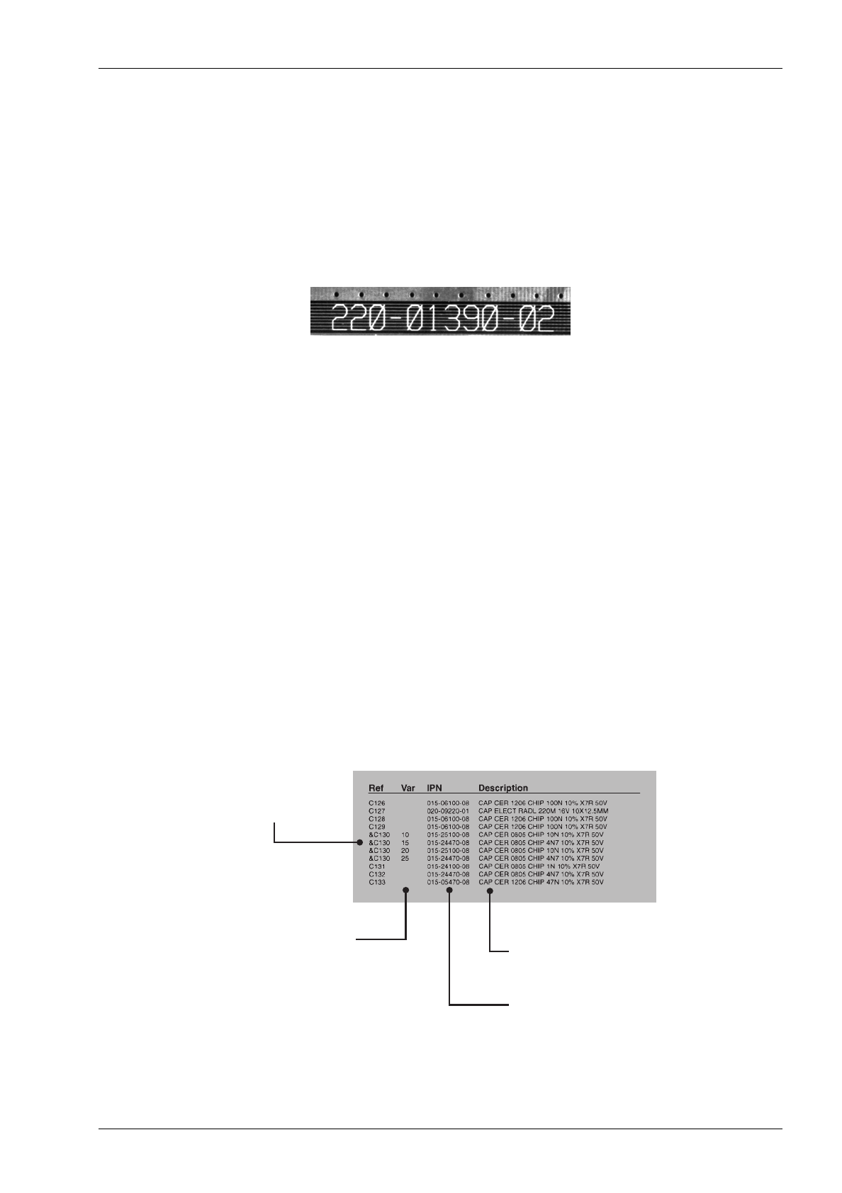
M830-00
Introduction
E1.1
Copyright TEL 30/04/98
1 Introduction
PCB Identification
All PCBs are identified by a unique 10 digit “internal part number” (IPN), e.g. 220-12345-00, which
is screen printed onto the PCB (usually on the top side), as shown in the example below:
The last 2 digits of this number define the issue status, which starts at 00 and increments through 01,
02, 03, etc. as the PCB is updated. Some issue PCBs never reach full production status and are there-
fore not included in this manual. A letter following the 10 digit IPN has no relevance in identifying
the PCB for service purposes.
Note:
It is important that you identify which issue PCB you are working on so that you can
refer to the appropriate set of PCB information.
Parts Lists
The 10 digit numbers (000-00000-00) in this Parts List are “internal part numbers” (IPNs). We can
process your spare parts orders more efficiently and accurately if you quote the IPN and provide a
brief description of the part.
The components listed in this parts list are divided into two main types: those with a circuit refer-
ence (e.g. C2, D1, R121, etc.) and those without (miscellaneous and mechanical).
Those with a circuit reference are grouped in alphabetical order and then in numerical order within
each group. Each component entry comprises three or four columns, as shown below:
The mechanical and miscellaneous section lists the variant and common parts in IPN order.
circuit reference -
lists components
in alphanumeric
order
variant column -
indicates that this is
a variant component
which is fitted only to
the product type listed
Internal Part Number -
order the component
b
y
this number
description -
gives a brief description
of the component
E1.2
Introduction
M830-00
30/04/98 Copyright TEL
Parts List Amendments
At the front of the parts list is the Parts List Amendments box (an example of which is shown
below). This box contains a list of component changes which took place after the parts list and dia-
grams in this section were compiled. These changes (e.g. value changes, added/deleted compo-
nents, etc.) are listed by circuit reference in alphanumeric order and supersede the information
given in the parts list or diagrams. Components without circuit references are listed in IPN order.
The number in brackets at the end of each entry refers to the Tait internal Change Order document.
Variant Components
A variant component is one that has the same circuit reference but different value or specification in
different product types. Where two products share the same PCB, the term “variant” is also used to
describe components unplaced in one product. Variant components have a character prefix, such as
“&”, “=” or “#”, before the circuit reference (e.g. &R100).
The table below explains the variant prefixes used in T800 Series II products:
If the variant prefix is. . . the component will. . .
& change according to channel spacing
= change according to frequency stability
# change according to frequency band
% be placed or unplaced for special applications
*be unplaced in one product
(where two products share the same PCB)
Parts List Amendments
R306 Changed from 180Ωto 560Ω(036-13560-00) to increase sensitivity (71003).
circuit reference
or IPN description
of change
IPN of new
component Change Order
number
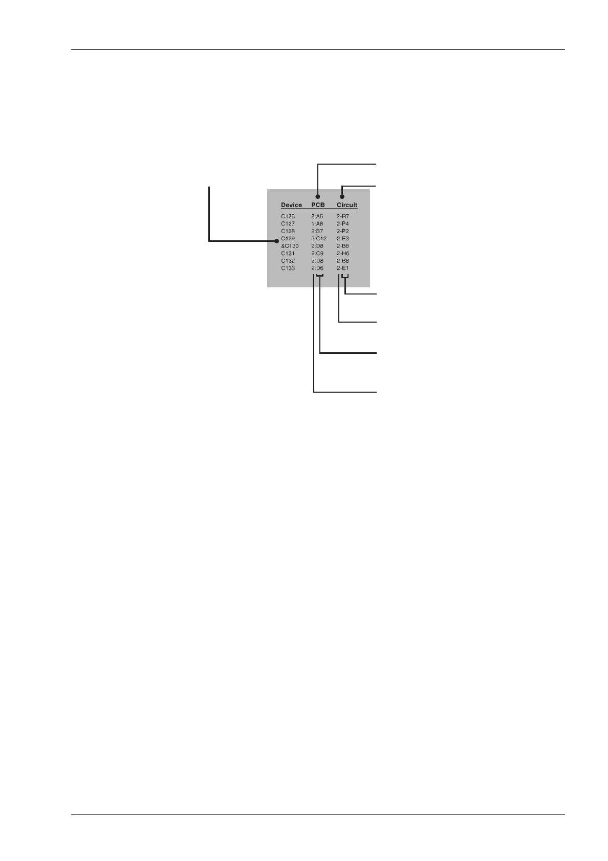
M830-00
Introduction
E1.3
Copyright TEL 30/04/98
Grid Reference Index
This section contains a component grid reference index to help you find components and labelled
pads on the PCB layouts and circuit diagrams. This index lists the components and pads in alpha-
numeric order, along with the appropriate alphanumeric grid references, as shown below:
circuit diagram
reference
PCB layout
reference
components listed
in alphanumeric order
layer number -
1 = top side layer
2 = bottom side layer
component location
on the layer
sheet number
component location
on the sheet


IPN 220-01176-03
M830-00
T830 VCO PCB Information
E2.3
Copyright TEL 23/07/99
T830 VCO Parts List (IPN 220-01176-03)
How To Use This Parts List
The components listed in this parts list are divided into two main types: those with a circuit reference (e.g. C2, D1, R121, etc.) and
those without (miscellaneous and mechanical).
Those with a circuit reference are grouped in alphabetical order and then in numerical order within each group. Each component
entry comprises three or four columns: the circuit reference, variant (if applicable), IPN and description. A letter in the variant column
indicates that this is a variant component which is fitted only to the product type listed. Static sensitive devices are indicated by an (S)
at the start of the description column.
The mechanical and miscellaneous section lists the variant and common parts in IPN order.
The Parts List Amendments box below lists component changes that took place after the parts list and diagrams in this section were
compiled. These changes (e.g. value changes, added/deleted components, etc.) are listed by circuit reference in alphanumeric order
and supersede the information given in the parts list or diagrams. Components without circuit references are listed in IPN order.
Parts List Amendments
#C6 Rx low (D): changed from 22p (015-22220-01) to 18p (015-22180-01) to improve loop voltage (710900).
Tx High (A): incorrectly listed as 22p (015-22220-01) - correct value is 18p (015-22180-01).
Tx High (A): changed from 18p (015-22180-01) to 15p (015-22150-01) to improve the loop voltage tuning range
at the top of the band (710943/44).

IPN 220-01176-03
E2.4
T830 VCO PCB Information
M830-00
30/04/98 Copyright TEL
Ref Var IPN Description Ref Var IPN Description
C2 015-23680-08 CAP CER 0805 680P 10% X7R 50V
#C3 A 015-22180-01 CAP CER 0805 18P 5% NPO 50V
#C3 B 015-22180-01 CAP CER 0805 18P 5% NPO 50V
#C3 C 015-22100-01 CAP CER 0805 10P+-1/2P NPO 50V
#C3 D 015-22100-01 CAP CER 0805 10P+-1/2P NPO 50V
#C4 A 015-22220-01 CAP CER 0805 22P 5% NPO 50V
#C4 B 015-22220-01 CAP CER 0805 22P 5% NPO 50V
#C4 C 015-22180-01 CAP CER 0805 18P 5% NPO 50V
#C4 D 015-22150-01 CAP CER 0805 15P 5% NPO 50V
#C5 A 015-22220-01 CAP CER 0805 22P 5% NPO 50V
#C5 B 015-22220-01 CAP CER 0805 22P 5% NPO 50V
#C5 C 015-22220-01 CAP CER 0805 22P 5% NPO 50V
#C5 D 015-22180-01 CAP CER 0805 18P 5% NPO 50V
#C6 A 015-22220-01 CAP CER 0805 22P 5% NPO 50V
#C6 B 015-22180-01 CAP CER 0805 18P 5% NPO 50V
#C6 C 015-22150-01 CAP CER 0805 15P 5% NPO 50V
#C6 D 015-22220-01 CAP CER 0805 22P 5% NPO 50V
#C7 A 015-22270-01 CAP CER 0805 27P 5% NPO 50V
#C7 B 015-22330-01 CAP CER 0805 33P 5% NPO 50V
#C7 C 015-22270-01 CAP CER 0805 27P 5% NPO 50V
#C7 D 015-22330-01 CAP CER 0805 33P 5% NPO 50V
C8 015-23120-01 CAP CER 0805 120P 5% NPO 50V
C9 015-23680-08 CAP CER 0805 680P 10% X7R 50V
C10 015-21220-01 CAP CER 0805 2P2+-1/4P NPO 50V
C11 015-23680-08 CAP CER 0805 680P 10% X7R 50V
C12 015-23680-08 CAP CER 0805 680P 10% X7R 50V
C13 025-08100-02 CAP TANT BEAD 10M 10% 16V
C14 015-23680-08 CAP CER 0805 680P 10% X7R 50V
C15 015-23680-08 CAP CER 0805 680P 10% X7R 50V
C16 015-22560-01 CAP CER 0805 56P 5% NPO 50V
C17 015-22560-01 CAP CER 0805 56P 5% NPO 50V
C18 015-23680-08 CAP CER 0805 680P 10% X7R 50V
C19 015-05470-08 CAP CER 1206 47N 10% X7R 50V
C20 015-23680-08 CAP CER 0805 680P 10% X7R 50V
C21 015-23680-08 CAP CER 0805 680P 10% X7R 50V
C22 015-23680-08 CAP CER 0805 680P 10% X7R 50V
C23 015-21820-01 CAP CER 0805 8P2+-1/4P NPO 50V
C24 015-21680-01 CAP CER 0805 6P8+-1/4P NPO 50V
C25 015-23680-08 CAP CER 0805 680P 10% X7R 50V
#C26 A 036-10000-00 RES M/F 0805 ZERO OHM
#C26 B 036-10000-00 RES M/F 0805 ZERO OHM
#C26 C 036-10000-00 RES M/F 0805 ZERO OHM
#C26 D 036-10000-00 RES M/F 0805 ZERO OHM
CV1 028-02111-00 16PF TRM CAP PISTON PREC.
D1 001-00012-63 S) DIODE VARICAP BB809
D2 001-00012-63 S) DIODE VARICAP BB809
D3 001-00012-63 S) DIODE VARICAP BB809
D4 001-00012-63 S) DIODE VARICAP BB809
L1 056-00021-56 IND FXD 3.3UH AX 10X4.2 PHEN
L2 056-00021-60 IND FXD 330NH AX N/MAG 6.6*2.7
#L3 A 055-01004-00 COIL TROID 103NH 22P 9T T830TX
#L3 B 055-01000-00 COIL TOROID 110NH 22P 10T T830
#L3 C 055-01003-00 COIL TROID 91NH 22P 8T T830RX
#L3 D 055-01004-00 COIL TROID 103NH 22P 9T T830TX
L4 056-00021-52 IND FXD 820NH 10% NON MAGNETIC
L5 056-00021-56 IND FXD 3.3UH AX 10X4.2 PHEN
L6 052-08135-35 COIL A/W 3.5T/3.5MM HOR 0.8MM
L7 056-00021-56 IND FXD 3.3UH AX 10X4.2 PHEN
L8 052-08130-45 COIL A/W 4.5T/3.0MM HOR 0.8MM
Q1 000-10003-10 S) XSTR SMD BFJ310 JFET UHF
Q2 000-10057-10 S) XSTR SMD BR571 NPN SOT23
Q3 000-10057-10 S) XSTR SMD BR571 NPN SOT23
Q4 000-10008-57 S) XSTR SMD BCW70 PNP SOT23 SS
Q5 000-00032-47 S) XSTR MRF559 NPN XPACK 0.5W
R1 036-12220-00 RES M/F 0805 22E 5%
R3 036-11470-00 RES M/F 0805 4E7 10%
#R5 A 036-13390-00 RES M/F 0805 390E 5%
#R5 B 036-13390-00 RES M/F 0805 390E 5%
#R5 C 036-13330-00 RES M/F 0805 330E 5%
#R5 D 036-13390-00 RES M/F 0805 390E 5%
R6 036-12560-00 RES M/F 0805 56E 5%
R7 036-14100-00 RES M/F 0805 1K 5%
R8 036-12560-00 RES M/F 0805 56E 5%
R9 036-14100-00 RES M/F 0805 1K 5%
R10 036-12100-00 RES M/F 0805 10E 5%
R11 036-14270-00 RES M/F 0805 2K7 5%
R12 036-13180-00 RES M/F 0805 180E 5%
R13 036-12220-00 RES M/F 0805 22E 5%
R14 036-12560-00 RES M/F 0805 56E 5%
R15 036-12220-00 RES M/F 0805 22E 5%
R16 036-13270-00 RES M/F 0805 270E 5%
R17 036-13270-00 RES M/F 0805 270E 5%
R18 036-12180-00 RES M/F 0805 18E 5%
R19 036-14100-00 RES M/F 0805 1K 5%
R20 036-14680-00 RES M/F 0805 6K8 5%
R21 036-14100-00 RES M/F 0805 1K 5%
R22 036-14220-00 RES M/F 0805 2K2 5%
R23 036-12180-00 RES M/F 0805 18E 5%
R24 036-12220-00 RES M/F 0805 22E 5%
R25 036-13220-00 RES M/F 0805 220E 5%
Variant
Code Description T835
(MHz) T836/837
(MHz)
A Tx high - 148 - 174
B Tx low - 136 - 156
C Rx high 169.4 - 195.4
D Rx low 157.4 - 177.4 -

IPN 220-01176-03
M830-00
T830 VCO PCB Information
E2.5
Copyright TEL 30/04/98
IPN Legend Description IPN Legend Description
T830 VCO Mechanical & Miscellaneous Parts (220-01176-03)
220-01176-03 PCB T83X VCO
240-00025-36 PLUG 32WAY 1ROW PC MTG HARWIN
345-00040-10 SCRW M3X6MM P/POZ ST BZ
345-00060-08 SCRW M5 X 16 CH SLOT PLASTIC
350-00016-42 SPACER 5MM HI 8MM ST 2.5MM HO
352-00010-14 NUT M5 HEX PLASTIC T800 TOROID
353-00010-10 WSHR M3 FLAT 7MMX0.6MM ST BZ
353-00010-13 WSHR M3 S/PROOF INT BZ
353-00010-41 WSHR M6 NYLON BULTE LOCK

IPN 220-01176-03
E2.6
T830 VCO PCB Information
M830-00
30/04/98 Copyright TEL
Device PCB Circuit Device PCB CircuitDevice PCB Circuit Device PCB Circuit
T830 VCO Grid Reference Index (IPN 220-01176-03)
How To Use This Grid Reference Index
The first digit in the PCB layout reference is a "1" or "2", indicating the top or bottom side layout respectively, and the last two charac-
ters give the location of the component on that diagram.
The first digit in the circuit diagram reference is the sheet number, and the last two characters give the location of the component on
that sheet.
C2 1:B7 1-B3
#C3 1:C6 1-D4
#C4 1:C6 1-D4
#C5 1:D6 1-D3
#C6 1:C5 1-E4
#C7 1:D5 1-E3
C8 1:D6 1-F3
C9 1:D4 1-H3
C10 1:C4 1-F3
C11 1:C4 1-G4
C12 1:D8 1-F6
C13 1:D7 1-G6
C14 1:C3 1-G5
C15 1:C4 1-H5
C16 1:B3 1-J5
C17 1:B3 1-J4
C18 1:B2 1-J5
C19 1:D1 1-J6
C20 1:D3 1-J7
C21 1:E3 1-K6
C22 1:C3 1-K5
C23 1:C2 1-K4
C24 1:C2 1-L4
C25 1:C2 1-L5
#C26 1:C5 1-D4
C40 1:D5 1-D3
CV1 1:C5 1-D3
D1 1:C7 1-B4
D2 1:C7 1-C4
D3 1:D7 1-B3
D4 1:D7 1-C3
L1 1:C8 1-B3
L2 1:B7 1-C3
#L3 1:B6 1-D4
L4 1:D6 1-E3
L5 1:D7 1-F6
L6 1:A4 1-J4
L7 1:D2 1-K6
L8 1:C2 1-L5
PL-2 2:B4 2-F3
PL-3 2:C3 2-G3
PL-4 2:C8 2-F4
PL-5 2:C1 2-G4
Q1 1:C6 1-F3
Q2 1:D4 1-G3
Q3 1:C4 1-G4
Q4 1:D2 1-K7
Q5 1:B3 1-K5
R1 1:B8 1-B3
R3 1:C7 1-C4
#R5 1:D6 1-F3
R6 1:D4 1-G3
R7 1:D3 1-G3
R8 1:D4 1-G3
R9 1:D3 1-G4
R10 1:C4 1-G4
R11 1:C3 1-G5
R12 1:C4 1-G5
R13 1:B3 1-G6
R14 1:C7 1-F5
R15 1:D8 1-G6
R16 1:B4 1-H4
R17 1:A4 1-H4
R18 1:B4 1-H5
R19 1:B4 1-H6
R20 1:E2 1-J6
R21 1:B2 1-K6
R22 1:D2 1-J7
R23 1:D2 1-K7
R24 1:B2 1-K5
R25 1:C3 1-K5
IPN 220-01176-03
E2.8
T830 VCO PCB Information
M830-00
30/04/98 Copyright TEL
T830 VCO PCB (IPN 220-01176-03) - Top Side
*C26
*C3
*C4 *C5
*C6 *C7
*L3
*R5
C10
C11
C12
C13
C14
C15
C16
C17
C18
C19
C2
C20
C21
C22
C23
C24
C25
C40
C8
C9
CV1
D1
D2
D3D4
L1
L2
L4
L5
L6
L7
L8
PCB
Q1
Q2
Q3
Q4
Q5
R1
R10
R11
R12
R13
R14
R15
R16
R17 R18
R19
R20
R21
R22
R23
R24
R25
R3
R6
R7
R8
R9
SCREW1
SCREW2
SCREW3
TBADMARK
*C26
*C3
*C4 *C5
*C6 *C7
*L3
*R5
C10
C11
C12
C13
C14
C15
C16
C17
C18
C19
C2
C20
C21
C22
C23
C24
C25
C40
C8
C9
CV1
D1
D2
D3D4
L1
L2
L4
L5
L6
L7
L8
PCB
Q1
Q2
Q3
Q4
Q5
R1
R10
R11
R12
R13
R14
R15
R16
R17 R18
R19
R20
R21
R22
R23
R24
R25
R3
R6
R7
R8
R9
SCREW1
SCREW2
SCREW3
TBADMARK
3
2
1
4
5
6
7
8
ABCDE

M830-00
FI
Copyright TEL 23/07/99
Part F Installation
This part of the manual is divided into the sections listed below. These sections give a
brief description of the basic rack mounting and wiring procedures for the T835
receiver, T836 transmitter, T837 exciter and T838/839 power amplifiers.
Section Title Page
1
1.1
1.2
1.3
1.4
T835 Installation
Rack Mounting
Rack Wiring
Power Supply
Reverse Polarity & Overvoltage Protection
1.1
1.1
1.1
1.2
1.2
2
2.1
2.2
2.3
2.4
T836/837 Installation
Rack Mounting
Rack Wiring
Power Supply
Reverse Polarity & Overvoltage Protection
2.1
2.1
2.1
2.2
2.2
3
3.1
3.2
3.3
3.4
T838/839 Installation
Rack Mounting
Rack Wiring
Power Supply
Reverse Polarity & Overvoltage Protection
3.1
3.1
3.1
3.2
3.2
4 N-Type Connector Assembly 4.1
Figure Title Page
1.1
1.2
1.3
1.4
T800-41-0002 Double Guide Kit
T835 Chassis Connectors
T835 D-Range 1 Wiring - Rear View
T835 D-Range 2 Wiring - Rear View (T800-03-0000 Kit)
1.1
1.1
1.1
1.1
2.1
2.2
2.3
2.4
T800-41-0002 Double Guide Kit
T836/837 Chassis Connectors
T836/837 D-Range 1 Wiring - Rear View
T836/837 D-Range 2 Wiring - Rear View (T800-03-0000 Kit)
2.1
2.1
2.1
2.1

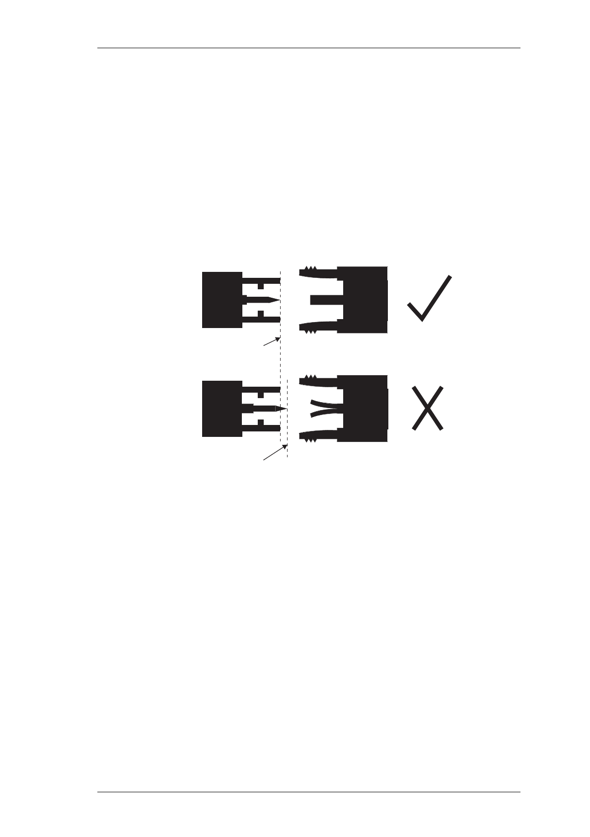
M830-00
N-Type Connector Assembly
F4.1
Copyright TEL 23/07/99
4 N-Type Connector Assembly
Make sure that any N-type plugs connected to Tait equipment are assembled according
to the manufacturer’s instructions. It is particularly important that the centre pin in the
plug is positioned correctly:
• if the pin is positioned too far back in the plug, it may not make good contact
with the socket;
• if the pin protrudes too far (as shown in Figure 4.1), or is not straight, it may
damage the socket when the plug is screwed in.
Figure 4.1 N-Type Plug Assembly Details
Hand ti
g
hten only
N-Type Plug and Socket Cross-section
Correct pin position No damage to socket
Will damage socket
Extended pin position


M830-00
GI
Copyright TEL 30/04/98
Part G System Configurations
This part of the manual is divided into the sections listed below. These sections provide
some brief information on basic system types and how to configure T830 Series II equip-
ment for use in them.
Section Title Page
1
1.1
1.2
1.3
1.4
1.5
1.6
1.7
1.7.1
1.7.2
T835 Link Selectable Features
Flat Or De-emphasised Response
Mute Relay Control
Mute Selection
Receiver Disable
CTCSS Configuration
300Hz High Pass Filter
Audio Processor Links
General
Audio Processor Linking Details For CTCSS
1.1
1.1
1.1
1.1
1.1
1.1
1.2
1.2
1.2
1.3
2
2.1
2.1.1
2.1.2
2.2
2.3
2.4
2.5
2.6
T836/837 Optional Features
Audio Processor
Link Details
Typical Options
Line Transformer Inputs And Outputs
Opto Key
Relay Driver
Local Microphone
Keying With Option PCBs
2.1
2.1
2.1
2.2
2.2
2.2
2.2
2.3
2.3
3 Talk Through Repeater 3.1
4
4.1
4.2
Line Controlled Base Without Talk Through
General
Transmitter Tail Timer
4.1
4.1
4.2
5 DC Line Keying 5.1

GII
M830-00
30/04/98 Copyright TEL
Figure Title Page
3.1
4.1
4.2
4.3
4.4
5.1
5.2
5.3
5.4
Talk Through Repeater
Basic Configuration
Remote Line Controlled Base Station
4-Wire to 2-Wire Convertor
Receiver Disable Time vs Tail Time
DC Loop Keying With Common Earth
Isolated Constant Current Loop Current Detector
Isolated Loop Current Switch
Typical System
3.1
4.1
4.1
4.2
4.2
5.1
5.1
5.2
5.2

M830-00
T835 Link Selectable Features
G1.1
Copyright TEL 23/07/99
1 T835 Link Selectable Features
1.1 Flat Or De-emphasised Response
The links of PL210 and PL220 may be set to give either a flat or de-emphasised audio
frequency response (refer to Section 1.7 for further details).
1.2 Mute Relay Control
A relay with undedicated contacts (RL210) is available in the audio processor circuit
block for various switching applications. A link (PL270) is available for control of the
relay from the mute circuit (refer to Section 1.7). This makes the relay suitable for con-
trolling the keying of a transmitter in repeater applications.
1.3 Mute Selection
Link PL250 may be set to operate with noise mute or carrier mute (refer to Section 1.7).
1.4 Receiver Disable
The receiver audio can be disabled by pulling the RX-DISABLE line low. When the cir-
cuit is pulled from low to high, the receiver audio cannot be re-enabled until the disable
timer completes its operation. This time is variable from 15ms to 200ms by adjusting
RV220 in the audio processor section.
If required, the operation of this circuit can be disabled by changing the link of PL260
from 1-2 to 2-3.
Typical applications of the receiver disable are as an extra mute for signalling purposes,
or when the T835 is configured as a line controlled base station (refer to Section 4).
1.5 CTCSS Configuration
Links PL230 & PL240 select various CTCSS options (refer to Section 1.7.2).

G1.2
T835 Link Selectable Features
M830-00
30/04/98 Copyright TEL
1.6 300Hz High Pass Filter
Link PL240 also allows the insertion of this filter to improve hum and noise perform-
ance.
1.7 Audio Processor Links
The tables in this section are the same as those in Section 3.5 in Part B. They have been
repeated here for ease of reference.
1.7.1 General
Use the following table to set up the audio processor to the configuration you require.
You should set the audio processor links before carrying out the receiver alignment.
The factory settings are shown in brackets [ ].
*Refer to Section 1.7.2 for further details.
Plug Link Function
PL210 [1 - 2]
2 - 3 de-emphasised response
flat response
PL220 1 - 2
[2 - 3] flat response
de-emphasised response
PL230* 1 - 2
[2 - 3]
3 - 4
audio input via AUDIO-2 pad
audio from internal CTCSS speech filter
audio input via I/O pad P250
PL240*
1 - 2
[2 - 3]
or
3 - 4
4 - 5
bypass high pass filter
300Hz high pass filter in circuit
audio input via PL230 or I/O pad
PL250 [1 - 2]
2 - 3 noise mute
carrier mute
PL260 1 - 2
[2 - 3] RX-DISABLE link
not connected
PL270 [1 - 2]
2 - 3 relay link
not connected

M830-00
T835 Link Selectable Features
G1.3
Copyright TEL 30/04/98
1.7.2 Audio Processor Linking Details For CTCSS
You must connect the audio processor links correctly according to the CTCSS option
used, as shown in the table below.
The conditions stated in the above table are defined as follows:
• standard, no CTCSS - no CTCSS or other sub-audio signalling used
- audio bandwidth 300Hz to 3kHz
- hum & noise -55dB
• received CTCSS tone - tone and speech transmitted down 600 ohm line
+ speech to line output - audio bandwidth 10Hz to 3kHz
- hum & noise -45dB
• high pass filtered speech - 400Hz to 3kHz
+ internal CTCSS detection - hum & noise -30dB with 250.3Hz tone present
• external CTCSS detection - decoding performed through the receiver (but
externally)
- speech injected back into receiver via "AUDIO-2"
and sent down 600 ohm line
Note 1:
AUDIO-2 is available on D-range 1 (PL100) pin 7 via the link resistor R160.
Although PL100 pin 7 is already assigned to SERIAL-COM, this can be disa-
bled by removing R808.
Note 2:
External CTCSS units can connect in series with the audio chain via
AUDIO-1 and AUDIO-2.
CTCSS Option PL230 PL240
standard, no CTCSS 2 - 3 2 - 3
received CTCSS + speech
passed to line output 3 - 4 1 - 2
high pass filtered speech,
internal CTCSS detection 2 - 3 4 - 5
external CTCSS detection 1 - 2 4 - 5


M830-00
T836/837 Optional Features
G2.1
Copyright TEL 30/04/98
2 T836/837 Optional Features
2.1 Audio Processor
The T836 and T837 come with a number of link selectable features which give added
system flexibility.
Note:
The tables in this section are the same as those in Section 3.5 in Part C. They
have been repeated here for ease of reference.
2.1.1 Link Details
Use the following table to set up the audio processor to the configuration you require.
You should set the audio processor links before carrying out any of the tuning and
adjustment procedures. The factory settings are shown in brackets [ ].
Plug Linka
a. The letters in this column and in the table in Section 2.1.2 below refer to the identification
letters screen printed onto the PCB beside each pair of pins.
Function
PL205
1-2
[3-4]
5-6
A
B
C
not connected
microphone pre-amp. output to compressor input
microphone pre-amp. output to multiplexer input
PL210
[1-2]
3-4
5-6
L
M
N
multiplexer output to pre-emphasis input
multiplexer output to limiter input
multiplexer output to compressor input
PL215
1-2
[3-4]
5-6
7-8
9-10
G
H
I
J
K
not connected
compressor output to multiplexer input
compressor output to limiter input
compressor output to pre-emphasis input
not connected
PL220
1-2
[3-4]
5-6
D
E
F
pre-emphasis output to multiplexer input
pre-emphasis output to limiter input
not connected

G2.2
T836/837 Optional Features
M830-00
30/04/98 Copyright TEL
2.1.2 Typical Options
2.2 Line Transformer Inputs And Outputs
The line transformer (T210) is designed to provide a balanced interface to 600 ohm lines.
For normal operation the two centre connections (LINE I/P 2, LINE I/P 3) are shorted
together, and the 600 ohm line is connected between LINE I/P 1 and LINE I/P 4.
The secondary winding of the transformer is connected via 1k and 10Ω (R160) resistors
to pin 6 (AUDIO-2) of D-range 1 and may be used to monitor audio on the line. Pin 7 of
D-range 1 can be reconfigured as AUDIO-1 by removing R808 and R160, and placing
%R150 (refer to Section 2 in Part I for more details).
2.3 Opto Key
The keying circuitry may be completely isolated from the rest of the system by means of
the optocoupler (IC250) connected between pins 11 and 12 of the D-range connector. A
constant current source (Q270) allows keying voltages between 6 and 50V.
2.4 Relay Driver
A dedicated transistor (Q250) is provided for the purpose of switching an external (e.g.
coaxial) relay. The output is open collector and is activated by the Tx-reg rail. This out-
put is available on pin 9 of the T800-03-0000 auxiliary D-range connector (D-range 2).
PL205 PL210 PL215 PL220
microphone pre-amp. compressed
and pre-emphasised;
line input pre-emphasised
(standard set-up)
[3-4]
B
[1-2]
L
[3-4]
H
[3-4]
E
microphone pre-amp. compressed
and pre-emphasised;
line input unprocessed
3-4
B
3-4
M
7-8
J
1-2
D
line and microphone compressed
and pre-emphasised
5-6
C
5-6
N
7-8
J
3-4
E
microphone pre-amp. compressed;
line and microphone flat response
3-4
B
3-4
M
3-4
H
5-6
F

M830-00
T836/837 Optional Features
G2.3
Copyright TEL 30/04/98
2.5 Local Microphone
Use of the local microphone (via the front panel stereo socket) will disable the audio
input from the line. The audio switching occurs when the PTT switch is closed.
2.6 Keying With Option PCBs
If an option PCB is fitted, the exciter may be keyed via the TX-ENB-OPT pad in the
audio processor. The line must be pulled low to key.

M830-00
Talk Through Repeater
G3.1
Copyright TEL 30/04/98
3 Talk Through Repeater
In this configuration the receiver directly keys the transmitter when the signal is
received. The demodulated audio is fed via 600 ohm lines to the transmitter to modu-
late the carrier. The receiver and transmitter operate simultaneously and must therefore
be on different frequencies. The minimum frequency separation depends on the
duplexer used.
Figure 3.1 Talk Through Repeater
Duplexer
Receiver Transmitter
Monitor
Speaker Local
Microphone
13.8V
Supply
+
-
Tx Key Out
Line Out Line In
Tx Key In
Antenna
Typical line level -15dBm
Monitor
Out Mic.
In
Transmit PortReceive Port
RF In
'N' Socket RF Out
'N' Socket

M830-00
Line Controlled Base Without Talk Through
G4.1
Copyright TEL 30/04/98
4 Line Controlled Base Without Talk
Through
4.1 General
This installation contains a transmitter and receiver which may or may not be on the
same frequency, thus simultaneous transmission and reception is not possible. When
the transmitter is keyed, the coaxial relay is also energised. When the relay is in its rest
position, signals from the aerial are passed to the receiver and the demodulated output
is fed via 600 ohm lines to the RCU.
The receiver is disabled when the transmitter is energised to prevent the receiver mute
opening from RF due to lack of isolation in the relay, direct radiation or the noise skirt of
the dual frequency link.
Since the base station may be controlled via a 2-wire line and a 4-wire to 2-wire hybrid,
there is a possibility of system oscillation if the receiver is not disabled during transmit.
This occurs when the transmit energy enters the receiver and produces an audio
response which can pass from the receive to the transmit audio part of the hybrid
(impedance imbalance, etc).
Figure 4.1 Basic Configuration
Figure 4.2 Remote Line Controlled Base Station
RF Out Coax
Relay
DC
Key
Logic
Tx
Enable
DC Relay
Control
RF In
Tx Rx
Antenna
Rx Disable
Tx AF
RF Out Coax
Relay
RF In
Tx Rx
Antenna
Hybrid
Rx AF
Remote
Control
Microphone
Speaker
PTT
G4.2
Line Controlled Base Without Talk Through
M830-00
30/04/98 Copyright TEL
Figure 4.3 4-Wire to 2-Wire Converter
4.2 Transmitter Tail Timer
If the transmitter has the tail timer enabled:
• the receiver disable timer must be set so that tRx/Dis > tTx/Tail;
Figure 4.4 Receiver Disable Time vs Tail Time
• if the system configuration also uses an aerial changeover relay as well as the tail
timer, the changeover relay must be driven from the relay driver (Q250) in the
audio processor, rather than by Tx key or Tx enable; this output is available on
pin 9 of the T800-03-000 auxiliary D-range (D-range 2);
• depending on tail time requirements, it is possible for the transmitter tail time to
exceed the receiver disable time capability; in this situation the receiver disable
line should also be driven from relay driver Q250 (D-range 2 pin 9).
2-Wire Line
C1
C2
TransmitterReceiver
RV1 approx. 2µ
Hybrid Balance
1k
Rx Disable Time
No Tx or Rx
Tail Time
On
Tx Reg.
Rx Off
Tx Enable
& Rx Disable
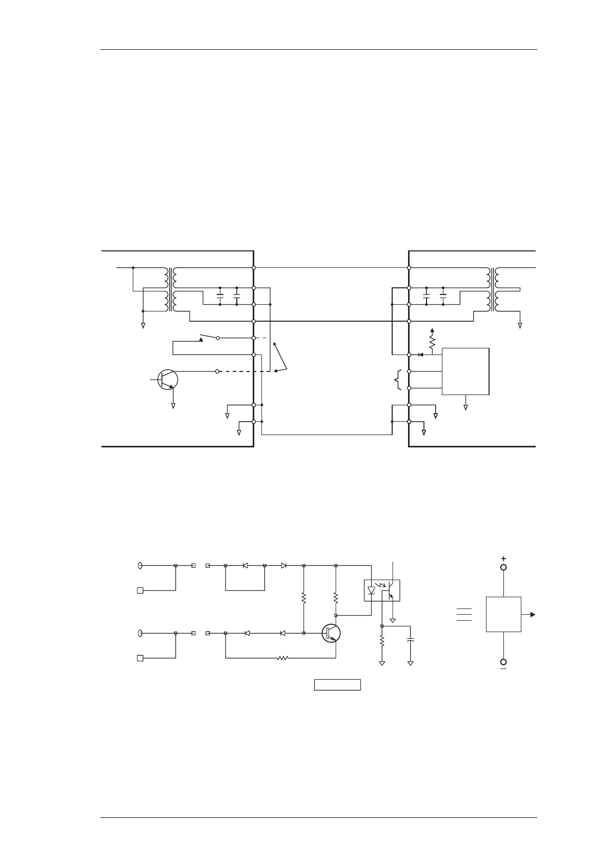
M830-00
DC Line Keying
G5.1
Copyright TEL 30/04/98
5 DC Line Keying
Where the transmitter and receiver are separated by only a short distance and DC isola-
tion is not required, DC loop keying may be employed.
A small DC current (usually less than 10mA) can be fed via the balanced 2-wire line to
provide remote control of various functions.
In a duplex system the receiver mute is used to key a transmitter, provided there is a
common earth between the two units (refer to Figure 5.1).
Figure 5.1 DC Loop Keying With Common Earth
Where the receiver and transmitter (or remote control) are distant, DC loop keying is
provided by an isolated supply, driver and detector because an earth cannot be relied on
(refer to Figure 5.2, Figure 5.3 & Figure 5.4).
Figure 5.2 Isolated Constant Current Loop Current Detector
(Opto-key input on T836 & T837)
Pin 14
Pin 12
Pin 1 (PL100)
Pin 3
Tx Key Pin 13
Pin 1
Pin 2
Pin 3
Pin 4
Pin 12
Pin 11
Pin 15
Pin 14
C266
8
4
3
5
6
27
1
Audio
Out T210
C268
RL210
Pin 13
C202
1
5
6
4
3
7
2
8
T210
C201
Pin 4 (PL100)
Audio
Processor
Keying Logic
Pin 15
Earth
Pin 2
+
-
Opto Key
+9V
R657
D620
Optional:
Relay contact or
Q270 collector
can be used.
Receiver Transmitter
Short Line
Q270
Det.
SL203 D260 D260
OPTO-KEY+S/L BAW56 BAW56
2331
I/OPAD
P219
OPTO-KEY+
OPTO-KEY-
OPTO-KEY+
OPTO-KEY-
I/OPAD
P225
SL204
OPTO-KEY-S/L
D270 D270
BAV99 BAV99
13 32
R268
100
OPTO-KEY
Q270
BD139 R271
390K C275
120P
R269
10K R270
470
IC250
4N25A
15
264
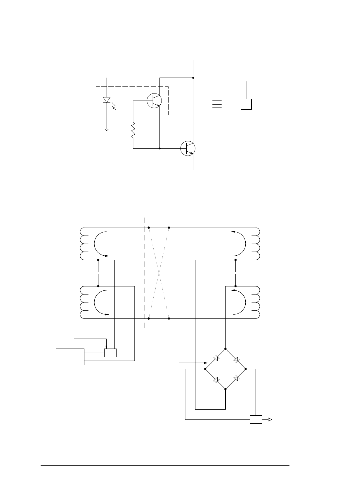

M830-00
HI
Copyright TEL 23/07/99
Part H T800 Ancillary Equipment
This Part of the manual features a brief description of the major ancillaries that may be
used with T800 Series II equipment. For a comprehensive list of available ancillary
equipment, please contact your nearest Tait Dealer or Customer Service Organisation.
Section Page
Programming Kits 1
General Ancillaries 2
Paging 5
External Frequency Reference 6
Rack Frames 7
Rack Frame Guides 9
Rack Frame PCBs 11
Rack Frame Ancillaries 12
Front Panels 13
Power Supplies 14


M830-00
T800 Ancillary Equipment
H1
Copyright TEL 23/07/99
T800 Ancillary Equipment
Programming Kits
T800-01-0000
The T800-01-0000 kit is used for programming T800 Series II base station equipment
using a standard IBM (or compatible) PC.
The kit comprises the following items:
PGM800Win programming software user's manual
PGM800Win Windows based programming software on 3 " floppy discs
T800-01-0002 programming cable.
T800-01-0001
The T800-01-0001 kit is the same as the T800-01-0000 kit described above, but with the
addition of the T800-01-0004 module programming interface.
T800-01-0002
The T800-01-0002 programming cable connects the PC directly to the programming
socket on the T800 Series II rack frame speaker panel or backplane PCB, thus enabling
T800 Series II modules to be read or programmed while in the rack frame. It can also
connect to the programming socket on the T800-01-0004 programming module interface
if the module is to be read or programmed while out of the rack frame.
T800-01-0003
The T800-01-0003 programming kit contains a T800-01-0002 programming cable and a
T800-01-0004 programming module interface.
T800-01-0004
The T800-01-0004 programming module interface is designed to allow a PC to connect
directly to a T800 Series II module. It comprises a small PCB on which is mounted a
D-range socket, a programming socket, a Micromatch socket and a DC input connector.
The T800-01-0004 plugs directly into D-range 1 or D-range 2 (selected by a switch on the
PCB), or into SK805 in the microcontroller compartment via the supplied ribbon cable
loom, and is then connected to the PC with a T800-01-0002 programming cable.
Refer to the T800 Ancillary Equipment Service Manual for more information.

H2
T800 Ancillary Equipment
M830-00
30/04/98 Copyright TEL
General Ancillaries
T004-72 RF Coaxial Relay
The T004-72 is an RF coaxial relay assembly fitted with three female N-type connectors,
and comes complete with a mounting bracket and two coaxial cables terminated in male
N-type connectors. It can be used, for example, in base station applications where the
receiver and transmitter share the same antenna, in which case it can be driven by the
T800 Series II transmitter/exciter relay driver (refer to Section 2.4 in Part G for more
information).
T800-01-0010 Calibration Test Unit
The T800-01-0010 provides all inputs and outputs necessary to carry out the full tuning
and adjustment procedure for T800 Series I and II receivers, exciters and transmitters. It
provides a convenient method of connecting test equipment, including a PC and power
supply, to a T800 Series I or II module (via D-range 1) without the need to construct cus-
tom wiring looms.
The T800-01-0010 also has a built-in speaker, a switch for selecting Series I or II modules,
and uses standard BNC and "banana plug" sockets.
Refer to the T800 Ancillary Equipment Service Manual for more information.
T800-03 Auxiliary D-Range
The T800-03 is an additional D-range kit comprising one D-range plug assembly and
two locating pins, nuts & washers. Although originally a T800 Series I ancillary, it can
be used in T800 Series II products for special applications requiring custom internal wir-
ing.
T800-03-0000 Auxiliary D-Range
The T800-03-0000 is an additional D-range kit (normally fitted as D-range 2) comprising
one D-range plug assembly complete with connecting loom and mounting screws. The
ribbon cable loom connects the D-range PCB to the Micromatch socket (SK805) in the
microcontroller compartment. Typical uses of the T800-03-0000 are in paging applica-
tions and where external channel control is required. Refer to Figure 1.4 and Figure 2.4
in Part F for the T800-03-0000 pin connections.

M830-00
T800 Ancillary Equipment
H3
Copyright TEL 23/07/99
T800-04-0000 RSSI
The T800-04 RSSI option PCB plugs directly into the main PCB (support circuitry being
fitted as standard). It is fitted to the T855, T875 and T885 whenever receiver signal
strength monitoring is required, e.g. trunking or voting. Its function is to provide a DC
voltage proportional to the signal level at the receiver input.
Refer to the appropriate service manual.
T800-08-0000 Ancillary Chassis
The T800-08-0000 is a general purpose chassis designed to be mechanically and elec-
tronically compatible with a T800 Series II rack frame. It comprises the following items:
• top and bottom chassis rails
•side panels
• rear panel
• PCB mounting brackets
• double D-range plug assembly (for mounting directly on a PCB)
• T800 Series II blank front panel complete with handle.
Custom designed PCBs for special applications can be mounted in several positions
inside the chassis to provide a convenient, plug-in module that interfaces directly with a
T800 Series II rack frame.
Refer to Technical Note TN-512 for further information.
T800-10-0000 Channel Select PCB
The T800-10-0000 is a small PCB that plugs into the Micromatch connector (SK805) in
the microcontroller compartment of a T800 Series II receiver, exciter or transmitter. It is
fitted with an eight-switch DIP switch which allows the manual selection of any one of
the channels already programmed into the module by PGM800Win. The T800-10-0000
is also fitted with a Micromatch socket to provide access to SK805 for programming pur-
poses.
T800-80 Local Microphone
A 600Ω microphone complete with 300mm cord terminated in a ¼" stereo plug.

H4
T800 Ancillary Equipment
M830-00
30/04/98 Copyright TEL
T818-01-0000 Receiver/Transmitter Monitor
The T818-01-0000 (formerly T318-02) is designed to monitor the basic operational func-
tions of one T800 receiver and transmitter. The meter and selector switches for monitor-
ing the required functions are mounted on the front panel, as is the monitor speaker
which is driven by a built-in amplifier. An optional mute circuit may be used to silence
the audio when no carrier is present.
Refer to M318-02.

M830-00
T800 Ancillary Equipment
H5
Copyright TEL 23/07/99
Paging
T800-30-0000 & T800-30-0002 DFSK Modulators
The T800-30-0000 (formerly T800-30) and T800-30-0002 (formerly T800-35) are DFSK
modulators for T800 Series II transmitters, suitable for POCSAG or similar paging data
formats. Analogue transmissions (e.g. tone or speech) are still possible by disabling the
data path via a control line. 512 or 1200 baud data rates are link selectable. The
T800-30-0002 is adapted for use with an external reference oscillator for simulcast trans-
mission. The T800-30-0000 and T800-30-0002 are not designed for use with 66 to 88MHz
equipment.
Refer to the T800 Ancillary Equipment Service Manual for more information.
T800-32-0000 & T800-32-0010 DFSK Modulators
The T800-32-0000 and T800-32-0010 are DFSK modulator PCBs which can be fitted to
T800 Series II transmitters to enable them to function as low-speed paging transmitters.
These new PCBs have been specifically designed for Series II transmitters and will be
much easier to fit into the latest design transmitters.
Both PCBs are suitable for POCSAG or similar paging data formats, but are not
designed for analogue transmissions (e.g. tone or speech). The T800-32-0010 is adapted
for use with an external reference oscillator for simulcast transmission. The T800-32-
0000 and T800-32-0010 are not designed for use with 66 to 88MHz equipment.

H6
T800 Ancillary Equipment
M830-00
23/07/99 Copyright TEL
External Frequency Reference
T800-06-0000 External Frequency Reference Kit
The T800-06-0000 kit provides an additional D-range plug/PCB assembly which incor-
porates a miniature RF connector to carry an externally generated 12.8MHz reference
signal into a T800 Series II module. This enables the use of very high stability external
reference oscillators for special applications.
The D-range PCB is also fitted with a Micromatch socket which can be connected to
SK805 in the microcontroller section via the supplied loom to provide access to the
channel change lines.
The kit comes complete with fitting instructions and all installation hardware.
T800-06-0001 External Frequency Reference Kit
The T800-06-0001 is the same as the T800-06-0000 kit with the addition of a special coax
cable for external frequency reference input. One end of this coax is terminated with a
miniature RF connector which fits into the D-range socket in an appropriate backplane
PCB (e.g. T800-52-0000) to connect to a T800 Series II module fitted with a T800-06-0000
kit. The other end is terminated with a BNC connector which can be mounted on the
rack frame.
T801 Frequency Reference Module
The T801 frequency reference module provides a high stability frequency source to
which the synthesiser within a T800 Series II base station can be locked. The master
standard within the T801 is primarily intended to be rubidium, although high quality
ovenised crystal oscillators can also be used in applications where more frequent read-
justment of frequency is acceptable. The T801 converts the output frequency from its
master standard to the 12.8MHz required by the T800 Series II base station.
Refer to M801-00.
T801-10 OCXO Module
The T801-10 OCXO module provides a high stability frequency source to which the syn-
thesiser within a T800 Series II base station can be locked. This will provide T800 Series
II transmitters with the frequency stability required for simulcast transmission. The
master standard within the T801-10 is a high quality ovenised crystal oscillator (OCXO).
Three outputs are provided on the rear panel, which allows up to three T800 Series II
transmitters to be referenced to the source oscillator.
Refer to M801-10.

M830-00
T800 Ancillary Equipment
H7
Copyright TEL 23/07/99
Rack Frames
T800-22-0000
The T800-22-0000 is a standard 5U high rack frame complete with wiring loom which is
designed to accommodate one 25, 50 or 100W base station or repeater. It comes fully
assembled with the following items:
T800-15-0000 speaker panel with programming port
T800-40-0001 blank panel (x2)
T800-41-0002 double module guide
T800-44-0000 power supply guide
T800-45-0000 PA guide
T800-50-0000 standard rack frame backplane PCB.
Refer to the T800 Ancillary Equipment Service Manual for more information.
T800-22-0001
The T800-22-0001 is the same as the T800-22-0000, but is supplied packed flat in disas-
sembled form for ease of transport. The wiring loom and backplane PCB are, however,
supplied complete and ready for installation.
T800-22-0002
The T800-22-0002 is a standard 5U high rack frame without wiring loom which is
designed to accommodate one 25, 50 or 100W base station or repeater. It comes fully
assembled with the following items:
T800-15-0000 speaker panel with programming port
T800-40-0001 blank panel (x2)
T800-41-0002 double module guide
T800-44-0000 power supply guide
T800-45-0000 PA guide.
T800-22-0003
The T800-22-0003 is the same as the T800-22-0002, but is supplied packed flat in disas-
sembled form for ease of transport.
T800-22-0004
The T800-22-0004 is a standard 5U high rack frame without wiring loom, guides or front
panels which comes fully assembled.

H8
T800 Ancillary Equipment
M830-00
23/07/99 Copyright TEL
T800-22-0005
The T800-22-0005 is the same as the T800-22-0004, but is supplied packed flat in disas-
sembled form for ease of transport.
T800-23-0000 Slimline Repeater Mounting Kit
The T800-23-0000 Slimline Repeater kit enables one T800 Series II receiver and one T800
Series II transmitter to be mounted horizontally side-by-side in a standard 483mm rack
frame. The kit contains a front panel complete with speaker, programming port, an
options tray (for mounting a power supply, duplexer, etc.), and a wiring loom to connect
the two T800 modules to the terminal blocks mounted on the rear of the options tray.
The T800-23-0010 mains power supply (available separately) is designed for use with
the T800-23-0000. The rack height of the assembled unit is 2U.
T800-23-0001 Slimline Repeater Mounting Kit
The T800-23-0001 Slimline Repeater kit is the same as the T800-23-0000, but is supplied
with a T800-23-0010 power supply and no options tray.

M830-00
T800 Ancillary Equipment
H9
Copyright TEL 23/07/99
Rack Frame Guides
T800-41-0001
The T800-41-0001 rack frame guide is designed to fit into a T800 Series II rack frame and
will accept one T800 Series II module (except for power supplies and power amplifiers
which must use their own guides). It is supplied disassembled and comprises a top and
bottom rail, a rear panel, two D-range sockets and mounting screws.
T800-41-0002
The T800-41-0002 rack frame guide is designed to fit into a T800 Series II rack frame and
will accept two T800 Series II modules (except for power supplies and power amplifiers
which must use their own guides). It is supplied disassembled and comprises two top
and bottom rails, a double width rear panel, four D-range sockets and mounting screws.
T800-41-0003
The T800-41-0003 rack frame guide is designed to fit into a T800 Series II rack frame and
will accept three T800 Series II modules (except for power supplies and power amplifi-
ers which must use their own guides). It is supplied disassembled and comprises three
top and bottom rails, a triple width rear panel, six D-range sockets and mounting
screws.
T800-41-0004
The T800-41-0004 rack frame guide is designed to fit into a T800 Series II rack frame and
will accept four T800 Series II modules (except for power supplies and power amplifiers
which must use their own guides). It is supplied disassembled and comprises four top
and bottom rails, a four-module wide rear panel, eight D-range sockets and mounting
screws.
T800-42-0000
The T800-42-0000 rack frame guide will allow a duplexer to be mounted in a T800 Series
II rack frame. It occupies a single module space and comprises a folded metal chassis,
mounting brackets and screws.

H10
T800 Ancillary Equipment
M830-00
23/07/99 Copyright TEL
T800-42-0001
The T800-42-0001 rack frame guide is the same as the T800-42-0000 described above, but
with the addition of a duplexer front panel.
T800-42-0002
The T800-42-0002 rack frame guide is the same as the T800-42-0000 described above, but
with the addition of a blank front panel.
T800-43-0000
The T800-43-0000 rack frame guide is designed to fit into a T800 Series II rack frame and
will accept one T300 or T1500 Series module (e.g. T318-02, T1511). It is supplied disas-
sembled and comprises a top and bottom rail, two T300 D-range socket boxes and
mounting screws. The T800-43-0000 is not compatible with the T800 Series II rack frame
backplane PCB. Consult your nearest Tait Dealer or Customer Service Organisation for
more details about T300/T1500 Series compatibility with T800 Series II rack frames.
T800-43-0001
The T800-43-0001 is the same as the T800-43-0000 but is supplied with only one D-range
socket box.
T800-44-0000
The T800-44-0000 rack frame guide is designed to fit into a T800 Series II rack frame and
will accept one T800 Series II power supply. It comprises a top and bottom rail and
mounting screws.
T800-45-0000
The T800-45-0000 rack frame guide is designed to fit into a T800 Series II rack frame and
will accept one T800 Series II 50W power amplifier. It comprises a top guide stop, a bot-
tom guide rail and mounting screws.
T800-45-0001
The T800-45-0001 rack frame guide is designed to fit into a T800 Series II rack frame and
will accept one T800 Series II 100W power amplifier. It comprises a top guide stop, a
bottom guide rail, extra mounting brackets for the double width front panel and mount-
ing screws.

M830-00
T800 Ancillary Equipment
H11
Copyright TEL 23/07/99
Rack Frame PCBs
T800-50-0000
The T800-50-0000 backplane PCB is designed to allow a T800-22-0000 rack frame to be
easily configured as either a base station or repeater. The PCB mounts across the rear
panel of the T800-41-0002 double module rack frame guide, enabling a T800 Series II
receiver and exciter/transmitter to plug directly into the D-range sockets provided on
the inner side of the PCB (both D-range 1 and D-range 2 are provided for). The other
side of the PCB features a programming port, D-range connectors which provide all
module inputs and outputs, and two DIP switches for external channel selection.
Refer to the T800 Ancillary Equipment Service Manual for more information.
T800-50-0001
The T800-50-0001 is similar in function and design to the T800-50-0000, but is designed
to allow connection of TA087 or TA387 channel select panels. It has one 25-way OEM
D-range connector, but will not accept personality PCBs.
T800-52-0000
The T800-52-0000 is similar in function and design to the T800-50-0000, but is designed
for use in Quasi-Sync applications. The PCB has an external reference D-range fitted
and has provision for connecting TA087 or TA387 channel change/speaker panels and a
TA136 alarm panel. The T800-52-0000 will not accept personality PCBs.
T800-60-0000
The T800-60-0000 personality PCB is designed to plug into the two 25-way D-range
sockets on the T800-50-0000 backplane PCB. The T800-60-0000 provides channel selec-
tion for both receiver and exciter/transmitter via a single DIP switch, remote channel
selection and alarm monitoring via Micromatch sockets, and receiver and exciter/trans-
mitter inputs and outputs via a 25-way D-range socket.

H12
T800 Ancillary Equipment
M830-00
23/07/99 Copyright TEL
Rack Frame Ancillaries
T800-13-0000 Extender Rail
The T800-13-0000 extender rail allows a T800 Series II receiver, exciter or transmitter to
be operated out of the rack frame with the covers off for tuning purposes. It is fitted
with two 15-way D-range connectors.
T800-14-0000 Extender Rail
The T800-14-0000 extender rail is the same as the T800-13-0000, but is intended for
equipment using an external reference (e.g. Quasi-Sync). It thus has one 15-way
D-range, and one 11-way D-range incorporating a miniature RF connector.
T800-19-0000 Rack Mounting Fan
The T800-19-0000 fan is designed to fit into the base of any standard 483mm rack frame
without affecting its ability to house seven modules. The two mounting rails are
secured to the rack frame side panels, and the fan is screwed onto the rails under the
required module. The kit contains all mounting hardware.
T800-19-0010 Rack Mounting Fan
The T800-19-0010 fan is designed to fit into the base of any standard 483mm rack frame
without affecting its ability to house seven modules. The fan is mounted directly onto
the underside of the bottom guide rails with two mounting brackets. The kit contains
all mounting hardware.

M830-00
T800 Ancillary Equipment
H13
Copyright TEL 23/07/99
Front Panels
T800-15-0000 Speaker Panel
A 60mm speaker panel fitted with a 4Ω speaker and programming socket. It comes
complete with mounting hardware and a cable to connect the programming socket to
the backplane PCB.
T800-15-0001 Speaker Panel
A 60mm speaker panel fitted with a 4Ω speaker, complete with mounting hardware.
T800-17-0010 Circuit Breaker Panel
A 60mm front panel fitted with a 10A magnetic circuit breaker. The circuit breaker also
functions as an on/off switch to control the supply of power to the rack frame. The
T800-17-0010 is intended primarily for use with rack frames powered by batteries (or
with a battery back-up supply) and comes complete with mounting hardware.
T800-17-0020 Circuit Breaker Panel
The same as the T800-17-0010, but fitted with a 20A circuit breaker.
T800-40-0000 Blank Panel Fitting Kit
The mounting brackets and screws necessary to fit a T800 Series II 60mm blank front
panel into a T800 Series II rack frame.
T800-40-0001 Blank Panel
A T800 Series II 60mm blank panel complete with mounting brackets and screws.

H14
T800 Ancillary Equipment
M830-00
23/07/99 Copyright TEL
Power Supplies
T800-23-0010 Mains Power Supply
The T800-23-0010 mains power supply is designed to power the T800-23-0000 Slimline
Repeater and mounts on the front panel instead of the options tray. It requires a mains
input voltage (auto range) of 85-132/170-264V AC at 47-440Hz.
Refer to the T800 Ancillary Equipment Service Manual for more information.
T807-10-0000 Mains Power Supply
The T807-10-0000 is a switching power supply capable of supplying up to 15A at 11-14V
DC. It requires a mains supply of 230V/50Hz or 115V/60Hz (nominal values) which
can be internally selected with a switch. The T807-10-0000 is designed to power T800
Series II 50W transmitters (plus receivers, etc.) and requires a T800-44-0000 guide to fit
into a T800 Series II rack frame.
Refer to the T800 Ancillary Equipment Service Manual for more information.
T808-10-0000 Mains Power Supply
The T808-10-0000 is a switching power supply capable of supplying up to 25A at 11-14V
DC. It requires a mains supply of 230V/50Hz or 115V/60Hz (nominal values) which
can be internally selected with a switch. The T808-10-0000 is designed to power T800
Series II 100W transmitters (plus receivers, etc.) and requires a T800-44-0000 guide to fit
into a T800 Series II rack frame.
Refer to the T800 Ancillary Equipment Service Manual for more information.

M830-00
I-I
Copyright TEL 30/04/98
Part I Using T830 Series II Equipment In A
Series I Rack Frame
This part of the manual describes how to modify T830 Series II equipment for operation
in a T800 Series I rack frame.
Section Title Page
1 Tools Required 1.1
2
2.1
2.2
T835/836/837 SII - SI Conversion
Introduction
Method
2.1
2.1
2.2
3
3.1
3.2
T838/839 SII - SI Conversion
Introduction
Method
3.1
3.1
3.2
Figure Title Page
2.1
2.2
2.3
T835 Component Changes
T836/837 Component Changes
T837 RF Output Coax Routing
2.3
2.5
2.7
3.1
3.2
T838/839 Component Changes
T838/839 RF Input Coax Routing
3.3
3.5


M830-00
Tools Required
I1.1
Copyright TEL 30/04/98
1 Tools Required
Tool Size
Allen Head Screwdriver 2mm AF
Flat Blade Screwdriver 3mm AF
Pozidriv Screwdrivers No. 1 for M3 screws No. 2 for M4 screws
Torx Screwdrivers T10 for M3 screws T20 for M4 screws
Spanners 1/4” AF for D-range locating pins
5.5mm AF for M3 nutsa
6mm AF for SMC connector
7mm AF for M4 nuts
a. If you do not have a 5.5mm spanner, you can use long-nosed pliers to carefully grip the M3 nuts on
the D-range securing screws and locating pins.
Solder
Soldering Iron


M830-00
T835/836/837 SII - SI Conversion
I2.1
Copyright TEL 23/07/99
2 T835/836/837 SII - SI Conversion
2.1 Introduction
You must make a number of modifications to enable a T830 Series II receiver, exciter or
transmitter to operate in a Series I rack frame. These changes can be split into two
groups, mechanical and electrical, as described below.
This procedure assumes you have already purchased the appropriate Series I conver-
sion kit:
• T835 - T800-70-0035
• T836 - T800-70-0036
• T837 - T800-70-0037.
If not, you should purchase one from your nearest Tait Dealer or Customer Service
Organisation before beginning the procedure.
It should take approximately 15-20 minutes per module to perform these steps.
Mechanical These changes involve:
• putting on a new front panel because of the differences in
height and width between a Series II and Series I panel;
• adding D-range locating pins as the Series I rack requires
them for alignment.
Electrical These changes involve:
• making sure there is pin compatibility for D-Range 1 pin 7
between the Series II module and the Series I rack frame;
in Series I, pin 7 is allocated to audio 1 for the transmitter/
exciter, and audio 2 for the receiver;
• converting the exciter from rear RF output to front RF out-
put;
• disabling cyclic keying in the exciter.

I2.2
T835/836/837 SII - SI Conversion
M830-00
30/04/98 Copyright TEL
2.2 Method
Step Action
1 Remove the Series II front panel from the module as follows:
• remove the volume knob (T835 only);
• remove the four screws using a Torx screwdriver;
• push the LEDs from the front of the panel to remove them from
their grommets.
2 Remove both covers from the module.
3 Remove the M3 screws, spring washers, and M3 nuts from D-range 1.
Note:
If you have a chassis with threaded holes, you will need to
remove only the M3 screws and spring washers.
4 Replace the M3 screws with locating pins, M3 spring washers (and nuts
if necessary).
5If you are modifying a T835, follow this step; otherwise go to Step 6.
Remove R808 (10Ω), as shown in Figure 2.1.
Ensure that R160 (10Ω) is placed, as shown in Figure 2.1.
This will convert D-range 1 pin 7 from serial com to audio 2.
Go to Step 8.
M830-00
T835/836/837 SII - SI Conversion
I2.3
Copyright TEL 30/04/98
Figure 2.1 T835 Component Changes
remove R808
ensure R160 is placed
&XF310&XF320
&XF330
&XF340
C201
C207
C209
C222
C229
C231
C233
C239
C240C
C249
C253
C260C
C261
C262
C266
C268
C305
C325
C340A
C348
C371
C373
C375
C390
C505
C515
C530
C535
C610A
C610B
C611A
C611B
C623
C625
C626
C628
C630
C631A
C631B
C637
C640
C651
C658
C660
C665
C670
C673
C677
C681
C684
C687
C690
C693
C700
C702
C703
C705
C707
C708
C709
C710A
C710B
C710C
C711
C712
C713
C735
C736
C740A
C740B
C741A
C741B
C742A
C742B
C743
C745
C750
C757
C759
C761
C762
C764
C765
C767
C769
C770
C772
C774
C776
C782
C784
C786
C788
C790 C792
C810
C812
C813
C814
C815
C816
C818
C819
C820
C822
C824
C826
C828
C830
C832
C833
C834
C836
C837
C838
C840
C842
C844
C846 C848
C850
C873
C876
C879
CV318
D111
D250
D280
D285
D289
D290
D295
D610
D640
D860
D880
IC210
IC240
IC260
IC270
IC280
IC340
IC350
IC390
IC410
IC610
IC630
IC640
IC650
IC700
IC710
IC740
IC750
IC820
IC830
IC840
IC850
L310
L330
L340
L350
L360
L410L420
L430
L440
L460L470
L480
L750
L910
L920
L930
P100
P160
P170
P201
P204
P207
P210
P213
P216
P219
P222
P225
P228
P231P234
P236
P238
P240
P242 P244
P246 P248
P250
P252
P254P256
P258
P260
P263
P266
P268
P270
P280
P282
P284
P287
P380
P810
P815
P820
P825
P830
P835 P840
PL100
PL210
PL220
PL230
PL240
PL250
PL260
PL270
Q310
Q540
Q620
Q630
Q660
Q670
Q750
Q760
Q770
Q775
Q780
Q785
Q790
Q795
Q810
Q820
Q840
Q850
Q860
Q870
Q880
Q890
Q895
R160
R351
R371
R510
R515
R555
R615
R617
R625
R633
R636
R637
R641 R645
R649
R653
R681
R685
R689
R693
R696
R701
R702
R703
R706
R707
R708
R709
R710
R711
R712
R742
R743
R744
R746
R747
R748
R749
R750
R752
R753
R754
R756
R757
R758
R759
R760
R762
R763
R765
R766
R767
R769
R771
R772
R774 R775
R784
R785
R786
R787
R790
R791
R792
R804
R805
R808
R809
R810 R811
R812
R813
R815
R816
R818
R819
R820
R821
R822
R823
R824
R825
R826
R827
R828
R829
R830
R831
R832
R833
R835
R836
R837
R840
R841
R842
R843
R844
R845
R846
R847
R848
R849R850
R851
R852
R853
R854
R855
R856
R857
R858
R859
R860
R861
R863
R865
R866
R867
R868
R869
R870
R871
R872R873
R875
R876
R877
R878
R879
R881
R882
R884
R885
R886
R887
R888
R889
R890
R891
R892
R894
R895R897
R898
RL210
RV220
RV235
RV320
RV330
SK805
SK810
T210
T610
T835
T835-
T83510
T83513
T83515
T83520
T83523
T83525
T835_
TOPFIDA
TOPFIDB
TOPHOLE
TOPSLOT
TP202
X310
1
2
3
4
5
6
7
8
9
ABCDEFGHJ KL MNPQ
1
2
3
4
5
6
7
8
9
ABCDEFGHJ KL MNPQ
T835 RECEIVER 220-01394-02
TP710
RV230
RV210
RV205
SW201
R297
L230
TP211
SK501
SK502
SK503
SK504
SK505
SK513
SK522 SK531
SK532
SK533
SK534
SK535
R629
R619
R621
TP601
TP607
TP604
TP603
SHLD610
TP602
L450
L490
L320
TP310
D820
D740
D730

I2.4
T835/836/837 SII - SI Conversion
M830-00
30/04/98 Copyright TEL
Step Action
6If you are modifying a T836, follow these steps (refer to Figure 2.2):
• remove R808 (10Ω)
• remove R160 (10Ω)
• place %R150 (10Ω).
Continue with Step 8.
If you are modifying a T837, follow these steps (refer to Figure 2.2):
• remove R808 (10Ω)
• remove R160 (10Ω)
• place %R150 (10Ω)
• remove L390; this will disable cyclic keying to enable the T837
to work with a Series I PA.
Continue with Step 7.
converts D-range 1 pin 7 from
serial com to audio 1
converts D-range 1 pin 7 from
serial com to audio 1
M830-00
T835/836/837 SII - SI Conversion
I2.5
Copyright TEL 23/07/99
Figure 2.2 T836/837 Component Changes
A LBDCE J NKMHGF P
Q
1
2
3
4
5
6
7
8
9
&C269
%C294
%C295
%C707
&R264
&R265
&R266
%R298
=R705
=SK710
C201 C202
C204
C205
C207
C209
C210
C211
C213
C215
C217
C219
C225
C227
C229
C230
C232
C233
C235
C237
C239
C241
C242
C243
C245
C259
C260
C261
C263
C265
C267
C271C273
C275
C277
C279
C281
C283
C285
C287
C289
C291
C293
C330B
C373
C385
C503
C505
C510
C513
C535
C550
C605
C610A
C610B
C611A
C611B
C623
C625
C626
C628
C630
C631A
C634
C636
C638
C640
C655
C660
C665
C670
C673
C677
C681
C684
C687
C690
C693
C700
C703
C705
C706
C708
C709
C710
C712
C720 C722
C724
C725
C726
C727
C729
C735
C736
C740A
C740B
C741A
C741B
C742A
C742B
C743
C745
C757
C759
C761
C762
C764
C765
C767
C769
C770
C772
C774
C776
C782
C784
C786
C788
C790
C792
C810
C812
C813
C822
C823C824
C826
C827
C828
C830
C838
C841
C844
C910
C920
C930
D111
D220
D230
D260
D270
D610
D620
D630
D635
D640
D710
D720
D730
D740
D810
IC210
IC220
IC230
IC260
IC330
IC610
IC630
IC640
IC650
IC710 IC720
IC730
IC740
IC750
IC820
IC830
L335
L345
L350
L360
L365
L375
L385
L750
P100
P150
P160
P170
P204
P208
P210
P211
P212
P219
P225
P230
P231
P233P235
P237 P239
P240
P243
P244
P245P247
P248
P249
P251
P255
P257
P259
P261
P263
P265
P267
P269
P271 P273
P275
P750
P805
P810
P820
P825
P830
P835
P840
PL100
Q210
Q220
Q230
Q240
Q250
Q315
Q365
Q370
Q510
Q520
Q530
Q540
Q550
Q610
Q620
Q630
Q660
Q670
Q710 Q720
Q730
Q740
Q750
Q760
Q770
Q775
Q780
Q785
Q790
Q795
Q810
Q820
Q830 Q840 Q850
Q860
R160
R201
R202
R204
R205
R206
R207
R208
R209
R210
R216
R217
R218
R219
R221
R223
R224
R225R226
R227
R229
R230
R231 R232
R233
R235
R237R238
R239
R241
R242
R244
R253
R254
R255
R256
R257
R258
R259
R260
R262
R263
R267
R268
R269
R270
R271
R272
R273
R274
R275
R277
R278
R279
R280
R282
R283
R284
R285
R286
R287
R288
R289
R290
R291 R292
R293
R294
R295
R296 R297
R299
R359
R360R362
R378 R380
R382
R388
R390
R392 R394
R396
R502
R505
R510
R515
R520
R525
R530
R535
R540
R545
R550
R555
R560
R609
R613
R615
R617
R625
R633
R637
R641 R645
R649
R653
R657
R661
R665
R669 R673
R677
R681
R685
R689R693
R696
R701
R702
R703
R706
R708R710
R711
R712
R713
R717
R718
R719
R720
R721
R722
R723
R725
R727
R728
R742
R743
R744
R746
R747
R748
R749
R750
R752
R753
R754
R756
R757
R758
R759
R760
R762
R763
R765
R766
R767
R769
R771
R772
R774
R775
R777
R784
R785
R786
R787
R790
R791
R792
R801
R802
R808
R809
R810 R811
R812
R813
R815
R816
R818
R819
R821
R822
R824
R825
R826
R827
R828
R829
R830
R831
R832
R833
R835
R836
R837
R840
R841
R842
R843
R845
R846
R847
R848
R849
R850
R853
R854
R855
R859
R861
R863
R865
R867
R871
R872
R873R874 R875
R876
R877
R879
RV220
RV805
SK310
SK420
T610
T837-
T83710
T83713
T83715
T83720
T83723
T83725
T837_
TOPFIDA
TOPFIDB
TOPHOLE
TOPSLOT
A LBDCE J NKMHGF PQ
1
2
3
4
5
6
7
8
9
SW230
RV210
SK205
T210
%D205
%D210
Q270
IC250
C221
C223
C247
C249
C251
C253
C255
C257
D240
D250
IC240
P215
P217
PL205PL210 PL220
Q260
R212
R213
R214
R215
R245
R247
R248
R249
R251
A
B
C
D
E
F
G
H
I
J
K
L
M
N
SID
COMPRESSION
LEVEL
LINE SENSITIVITY
CARRIER SWITCH
MIC/PRESSEL
L340
TP206 TP308
SL320
L370
L355
L390
L380
SK501
SK502
SK503
SK504
SK505
SK522
SK513
SK531
SK532
SK533
SK534
SK535
=IC700
C750
TP710
%C733
%R726
%C713
TP715
SK805
SK810
SL810
TP607
TP603
TP604
TP602
R619
TP601
R629
R621
PL215
T837
T837EXCITER
220-01390-02
%R715
DRANGE
AUX
CTCSS LEVEL ADJUST
%R150
L910L920
C373
C385
L335
L345
L350
L360
L365
L375
L385
Q365
Q370
R359
R360
R362
R378 R380
R382
R388
R390
R392
R394
R396
SK310
L340
TP308
SL320
L370
L355
L390
L380
remove L390
C810
C812
C822
C823
C824
C826
C827
C828
C830
C838
C841
C844
D111
D810
IC820
IC830
P150
P160
P170
P805
P810
P820
P825
P830
P835
P840
PL100
Q810
Q820
Q830 Q840 Q850
Q860
R160
R801
R802
R808
R809
R810
R811
R812
R813
R815
R816
R818
R819
R821
R822
R824
R825
R826
R827
R828
R829
R830
R831
R832
R833
R835
R836
R837
R840
R841
R842
R843
R845
R848
R849
R853
R854
R855
R859
R861
R863
R865
R867
R871
R872
R873
R874 R875
R876
R877
R879
RV805
SK805
SK810
SL810
TP607
DRANGE
AUX
CTCSS LEVEL ADJUST
%R150
remove R160place %R150
remove R808
(T837 only)

I2.6
T835/836/837 SII - SI Conversion
M830-00
30/04/98 Copyright TEL
Step Action
7Converting the T837 from rear panel RF output to front panel RF out-
put.
Desolder, unscrew and remove the rear panel N-type connector.
Fit the blanking plate over the hole in the chassis from which the N-type
connector has been removed.
Unplug the existing coax from SK310 and SK420, retaining the spring
clip for the new coax cable.
Fit the front panel SMC connector:
• insert the coax fitted with the brass SMC connector through the
hole in the front of the chassis and secure with the brass nut
and washer;
• connect the coax from the SMC connector into SK310, securing
the coax in the groove provided in the chassis wall with the
spring clip (refer to Figure 2.3).
8 Fit all parts of the Series I front panel, following Step 1 in reverse order.
Note:
If you have difficulty refitting the LEDs, try pushing the
body of the LED back into the grommet with a thin screw-
driver or spike. Be very careful while doing this as the legs
of the LED are very easy to break.
9 Replace the covers.
10 Programming
Once you have carried out this conversion procedure, you will no
longer be able to program the T830 Series II module via D-range 1.
In order to program the module now, you will need to use a program-
ming module interface, such as the T800-01-0004. This device is fitted
with a programming socket and can be connected to the module via
SK805 in the microcontroller section. You will have to remove the top
cover (closest to the handle) to gain access to SK805.
Note:
You may still be able to program the module by connecting
the T800-01-0004 to a T800-03-0000 auxiliary D-range fitted
as D-range 2, but only if pins 8 (ground) and 12 (serial com)
of D-range 2 are not used in the Series I configuration.
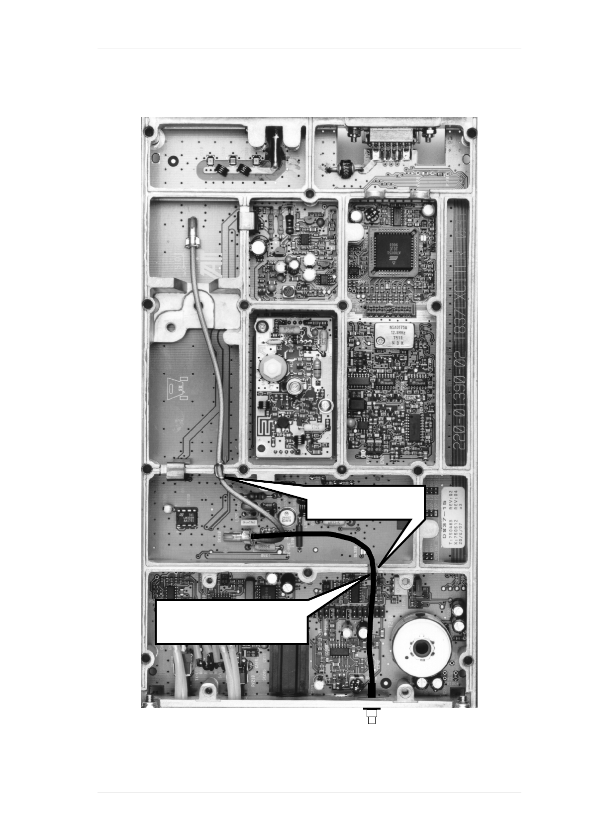


M830-00
T838/839 SII - SI Conversion
I3.1
Copyright TEL 23/07/99
3 T838/839 SII - SI Conversion
3.1 Introduction
You must make a number of modifications to enable a T830 Series II PA to operate in a
Series I rack frame. These changes can be split into two groups, mechanical and electri-
cal, as described below.
This procedure assumes you have already purchased the appropriate Series I conver-
sion kit:
• T838 - T800-70-0038
• T839 - T800-70-0039.
If not, you should purchase one from your nearest Tait Dealer or Customer Service
Organisation before beginning the procedure.
Note:
This procedure applies to the latest design T838/839 PAs which use RF
power modules and are identified by the Series II style product code
T83X-X0-0000.
It should take approximately 15-20 minutes per module to perform these steps.
Mechanical These changes involve putting on a new front panel because of the
differences in height and width between a Series II and Series I
panel.
Electrical These changes involve:
• inserting and removing components inside the module to
disable cyclic keying;
• converting from rear RF input to front RF input.
I3.2
T838/839 SII - SI Conversion
M830-00
30/04/98 Copyright TEL
3.2 Method
Step Action
1 Remove the Series II front panel from the PA as follows:
• remove the four screws using a Torx screwdriver;
• push the LEDs from the front of the panel to remove them from
their grommets.
2 Remove the side cover.
3 Follow the step for whichever module you are going to modify:
• T838 - go to Step 4;
• T839 - go to Step 5.
These modifications will disable the cyclic keying.
4T838
Remove *L201 (330nH SMD inductor), as shown in Figure 3.1.
Caution:
Do not use excessive heat to remove the inductor or it
will melt.
Place *R120 (0Ω SMD resistor), as shown in Figure 3.1.
5T839
Remove *L211 (330nH SMD inductor), as shown in Figure 3.1.
Caution:
Do not use excessive heat to remove the inductor or it
will melt.
Place *R120 (0Ω SMD resistor), as shown in Figure 3.1.
M830-00
T838/839 SII - SI Conversion
I3.3
Copyright TEL 30/04/98
Figure 3.1 T838/839 Component Changes
*RV111
LINK2
R135
R163
R166
R173
R174
TOPFIDB
RV109
D109
D103
D107
SERIES II ONLY
*C203
*C204
*C206
*L201
*R201
*R202
*R204
*SK203
*R208
C143
C145
C147
C149
C155
C173
C174
C176
C179
C180
C181
C182
C184
C185
C186
C187
C189
C215
C220
C221
C222
C223
C224
C226
D202
IC101
IC105
IC107
IC204
L105
L208
LINK1
LINK201
Q123
Q125
Q127
Q133
Q135
Q136
Q201
R101
R103
R104
R118
R119
R141
R142
R143
R144
R145
R146
R155
R156
R157
R168
R169
R170
R171
R172
R175
R176
R177
R178
R179
R180
R181
R182
R183
R184
R185
R186
R187
R188
R189
R190
R194
R195
R196
R197
R207
R209
R210
R212
R213
R214
R218
R220
R222
R224
R228
R229
*R107
*R122
*C123
*R116
*C212
*C213
*R211
*C121
*R105
*C103
*C101
*R120
*C124
*R102
*C127
Q137
*C217
*C219
*L211
*SK201
*C217
*C219
*C230
*C231*C232
*C233
*C234
*C240
*IC203*IC205
*L204
*L211
*L230
*L236
*Q109
*R111
*R208
*R216*R217
*R230
*R232
*RV111
*SK201
C129
C131
C132
C133
C137
C138
C139
C141
C143
C145
C147
C149
C151
C153
C155
C159
C161
C162
C164
C165 C167
C169
C171
C173
C174
C176
C178
C179
C180
C181
C182
C184
C185
C186
C187
C188
C189
C190
C192
C193
C195
C201
C205
C207
C215
C220
C221
C222
C223
C224
C225
C226
C227
C229
C259
C261
C294
C295
C297
C298
D101
D105
D111
D202
IC101
IC103
IC105
IC107
IC109
IC204
L101
L103
L105
L203
L208
L233
L239
L245 L248
L264
LINK1
LINK2
LINK201
P101
P103
P105
P201
PL101
Q111
Q113
Q115
Q117
Q119
Q121
Q123
Q125
Q127
Q129
Q131
Q133
Q135
Q136
Q201
R101
R103
R104
R117
R118
R119
R123
R124
R125
R126
R127
R128
R129
R130
R131
R132
R133
R134
R135
R136
R137
R138
R141
R142
R143
R144
R145
R146
R148
R149
R150
R151
R152 R153
R154
R155
R156
R157
R158
R159
R160
R161
R162
R163
R164
R165
R166
R168
R169
R170
R171
R172
R173
R174
R175
R176
R177
R178
R179
R180
R181
R182
R183
R184
R185
R186
R187
R188
R189
R190
R191
R192
R193
R194
R195
R196
R197
R203
R205
R207 R209
R210
R212
R213
R214
R218
R220
R222R224
R228
R229
R237
RV101RV103
RV105
RV107
RV113
RV115
SK101
SK103
TH201
TOPFIDA
TOPFIDB
TS202
C272
L249
C273
L247 L243
C271
C270
L241
R225
*#IC202
D113
R231
R219
L217
L215
*L223
*R215
RV109
*R113
*C117
*C119
*Q107
*C113
*C115
*R112
*C209
*C210
*R115
*R206
*R114
*Q105
*C111
*R107
*R122
*C123
*R116
*C212
*C213
*R211
*C121
*R105
*C103
*C101
*C124
*R102
*C127
*C125
*R121
*R109
*Q101
*R108
*C107
*C105
*R106
*Q103
*C109
*839-10R
*839-20R
*838-10R
*838-20R
*839-10F
*839-20F
*838-10F
*838-20F
*L231
D109
D103
D107
*L202
*C202
*C208
C216
L206
C218
Q137
*R223
C268
D203
D201
Control Circuitry
Low Pass Filter
Directional Coupler
RF OUT RF IN
REV PWR
FWD PWR
220-01402-02
#IC201
T839 ISSUE: 3A
220-01404-03
SERIES II ONLY
LC NG
4
MP
1K
2
HJ
3
D QB EFA
5
6
7
8
*RV111
C129
C131
C132
C133
C137
C138
C139
C141
C143
C145
C147
C149
C151
C153
C155
C159
C161
C162
C164
C165 C167
C169
C171
C173
C174
C176
C178
C179
C180
C181
C182
C184
C185
C186
C187
C188
C189
C190
C192
C193
C195
C201
C205
C207
C215
C220
C221
C222
C223
C224
C225
C226
C227
C229
C259
C261
C294
C295
C297
C298
D101
D105
D111
D202
IC101
IC103
IC105
IC107
IC109
IC204
L101
L103
L105
L203
L208
L233
L239
L245 L248
L264
LINK1
LINK2
LINK201
P101
P103
P105
P201
PL101
Q111
Q113
Q115
Q117
Q119
Q121
Q123
Q125
Q127
Q129
Q131
Q133
Q135
Q136
Q201
R101
R103
R104
R117
R118
R119
R123
R124
R125
R126
R127
R128
R129
R130
R131
R132
R133
R134
R135
R136
R137
R138
R141
R142
R143
R144
R145
R146
R148
R149
R150
R151
R152 R153
R154
R155
R156
R157
R158
R159
R160
R161
R162
R163
R164
R165
R166
R168
R169
R170
R171
R172
R173
R174
R175
R176
R177
R178
R179
R180
R181
R182
R183
R184
R185
R186
R187
R188
R189
R190
R191
R192
R193
R194
R195
R196
R197
R203
R205
R207 R209
R210
R212
R213
R214
R218
R220
R222R224
R228
R229
R237
RV101RV103
RV105
RV107
RV113
RV115
SK101
SK103
TH201
TOPFIDA
TOPFIDB
TS202
C272
L249
C273
L247 L243
C271
C270
L241
R225
D113
R231
R219
L217
L215
RV109
*839-10R
*839-20R
*838-10R
*838-20R
*839-10F
*839-20F
*838-10F
*838-20F
D109
D103
D107
C216
L206
C218
Q137
C268
D203
D201
Control Circuitry
Low Pass Filter
Directional Coupler
SERIES II ONLY
REV PWR
FWD PWR
#IC201
220-01404-03
*C203
*C204
*C206
*L201
*R201
*R202
*R204
*SK203
RF IN
RF OUT 220-01402-02 COAX LINK
T838 ISSUE: 3A
LC NG
4
MP
1K
2
HJ
3
D QB EFA
5
6
7
8
T838 - remove *L201
T838 & T839 - place *R120
T839 - remove *L211

I3.4
T838/839 SII - SI Conversion
M830-00
30/04/98 Copyright TEL
Step Action
6Converting from rear panel RF input to front panel RF input.
Remove the rear panel BNC connector:
• unplug the RF input coax from the socket on the PCB;
• unscrew the BNC connector from the chassis;
• carefully withdraw the coax from the module through the hole
in the rear of the chassis;
• fit the blanking plate over the hole in the chassis from which
the BNC connector has been removed.
Fit the front panel SMC connector:
• insert the coax fitted with the brass SMC connector through the
hole in the front of the chassis and secure with the brass nut
and washer;
• connect the coax from the SMC connector into *SK203 (T838) or
*SK201 (T839) as shown in Figure 3.2.
7 Refit the side cover.
8 Fit all parts of the Series I front panel, following Step 1 in reverse order.
Note:
If you have difficulty refitting the LEDs, try pushing the
body of the LED back into the grommet with a thin screw-
driver or spike. Be very careful while doing this as the legs
of the LED are very easy to break.
M830-00
T838/839 SII - SI Conversion
I3.5
Copyright TEL 30/04/98
Figure 3.2 T838/839 RF Input Coax Routing
*RV111
C129
C131
C132
C133
C137
C138
C139
C141
C143
C145
C147
C149
C151
C153
C155
C159
C161
C162
C164
C165 C167
C169
C171
C173
C174
C176
C178
C179
C180
C181
C182
C184
C185
C186
C187
C188
C189
C190
C192
C193
C195
C201
C205
C207
C215
C220
C221
C222
C223
C224
C225
C226
C227
C229
C259
C261
C294
C295
C297
C298
D101
D105
D111
D202
IC101
IC103
IC105
IC107
IC109
IC204
L101
L103
L105
L203
L208
L233
L239
L245 L248
L264
LINK1
LINK2
LINK201
P101
P103
P105
P201
PL101
Q111
Q113
Q115
Q117
Q119
Q121
Q123
Q125
Q127
Q129
Q131
Q133
Q135
Q136
Q201
R101
R103
R104
R117
R118
R119
R123
R124
R125
R126
R127
R128
R129
R130
R131
R132
R133
R134
R135
R136
R137
R138
R141
R142
R143
R144
R145
R146
R148
R149
R150
R151
R152 R153
R154
R155
R156
R157
R158
R159
R160
R161
R162
R163
R164
R165
R166
R168
R169
R170
R171
R172
R173
R174
R175
R176
R177
R178
R179
R180
R181
R182
R183
R184
R185
R186
R187
R188
R189
R190
R191
R192
R193
R194
R195
R196
R197
R203
R205
R207 R209
R210
R212
R213
R214
R218
R220
R222R224
R228
R229
R237
RV101RV103
RV105
RV107
RV113
RV115
SK101
SK103
TH201
TOPFIDA
TOPFIDB
TS202
C272
L249
C273
L247 L243
C271
C270
L241
R225
D113
R231
R219
L217
L215
RV109
*839-10R
*839-20R
*838-10R
*838-20R
*839-10F
*839-20F
*838-10F
*838-20F
D109
D103
D107
C216
L206
C218
Q137
C268
D203
D201
Control Circuitry
Low Pass Filter
Directional Coupler
SERIES II ONLY
REV PWR
FWD PWR
#IC201
220-01404-03
*C203
*C204
*C206
*L201
*R201
*R202
*R204
*SK203
RF IN
RF OUT 220-01402-02 COAX LINK
T838 ISSUE: 3A
LC NG
4
MP
1K
2
HJ
3
D QB EFA
5
6
7
8
*C217
*C219
*C230
*C231*C232
*C233
*C234
*C240
*IC203*IC205
*L204
*L211
*L230
*L236
*Q109
*R111
*R208
*R216*R217
*R230
*R232
*RV111
*SK201
C129
C131
C132
C133
C137
C138
C139
C141
C143
C145
C147
C149
C151
C153
C155
C159
C161
C162
C164
C165 C167
C169
C171
C173
C174
C176
C178
C179
C180
C181
C182
C184
C185
C186
C187
C188
C189
C190
C192
C193
C195
C201
C205
C207
C215
C220
C221
C222
C223
C224
C225
C226
C227
C229
C259
C261
C294
C295
C297
C298
D101
D105
D111
D202
IC101
IC103
IC105
IC107
IC109
IC204
L101
L103
L105
L203
L208
L233
L239
L245 L248
L264
LINK1
LINK2
LINK201
P101
P103
P105
P201
PL101
Q111
Q113
Q115
Q117
Q119
Q121
Q123
Q125
Q127
Q129
Q131
Q133
Q135
Q136
Q201
R101
R103
R104
R117
R118
R119
R123
R124
R125
R126
R127
R128
R129
R130
R131
R132
R133
R134
R135
R136
R137
R138
R141
R142
R143
R144
R145
R146
R148
R149
R150
R151
R152 R153
R154
R155
R156
R157
R158
R159
R160
R161
R162
R163
R164
R165
R166
R168
R169
R170
R171
R172
R173
R174
R175
R176
R177
R178
R179
R180
R181
R182
R183
R184
R185
R186
R187
R188
R189
R190
R191
R192
R193
R194
R195
R196
R197
R203
R205
R207 R209
R210
R212
R213
R214
R218
R220
R222R224
R228
R229
R237
RV101RV103
RV105
RV107
RV113
RV115
SK101
SK103
TH201
TOPFIDA
TOPFIDB
TS202
C272
L249
C273
L247 L243
C271
C270
L241
R225
*#IC202
D113
R231
R219
L217
L215
*L223
*R215
RV109
*R113
*C117
*C119
*Q107
*C113
*C115
*R112
*C209
*C210
*R115
*R206
*R114
*Q105
*C111
*R107
*R122
*C123
*R116
*C212
*C213
*R211
*C121
*R105
*C103
*C101
*C124
*R102
*C127
*C125
*R121
*R109
*Q101
*R108
*C107
*C105
*R106
*Q103
*C109
*839-10R
*839-20R
*838-10R
*838-20R
*839-10F
*839-20F
*838-10F
*838-20F
*L231
D109
D103
D107
*L202
*C202
*C208
C216
L206
C218
Q137
*R223
C268
D203
D201
Control Circuitry
Low Pass Filter
Directional Coupler
RF OUT RF IN
REV PWR
FWD PWR
220-01402-02
#IC201
T839 ISSUE: 3A
220-01404-03
SERIES II ONLY
LC NG
4
MP
1K
2
HJ
3
D QB EFA
5
6
7
8
Rear RF input coax
Front RF input coax
T838 T839
