Tait TEL0047 One way paging transmitters T836-26-1010 & T836-26 User Manual 8c300 a4 bk
Tait Limited One way paging transmitters T836-26-1010 & T836-26 8c300 a4 bk
Tait >
Contents
Manual

M830-00
CI
Copyright TEL 30/04/98
Part C T836 Transmitter & T837 Exciter
This part of the manual is divided into six sections, as listed below. There is a detailed
table of contents at the start of each section.
Section Title
1 General Information
2 Circuit Operation
3 Initial Tuning & Adjustment
4 Functional Testing
5 Fault Finding
6 PCB Information

M830-00
T836/837 General Information
C1.1
Copyright TEL 30/04/98
1 T836/837 General Information
This section provides a brief description of the T836 transmitter and T837 exciter, along
with detailed specifications and a list of types available.
The following topics are covered in this section.
Section Title Page
1.1 Introduction 1.7
1.2
1.2.1
1.2.2
1.2.3
1.2.4
1.2.4.1
1.2.4.2
1.2.4.3
1.2.5
1.2.6
Specifications
Introduction
General
RF Section
Audio Processor
Inputs
Modulation Characteristics
CTCSS
Microcontroller
Test Standards
1.8
1.8
1.8
1.9
1.10
1.10
1.10
1.11
1.12
1.12
1.3 Product Codes 1.13
1.4 T836 Standard Product Range 1.14
1.5 T837 Standard Product Range 1.15
Figure Title Page
1.1 T836 Main Circuit Block Identification 1.4
1.2 T836 Front Panel Controls 1.4
1.3 T837 Main Circuit Block Identification 1.6
1.4 T837 Front Panel Controls 1.6


M830-00
T836/837 General Information
C1.7
Copyright TEL 23/07/99
1.1 Introduction
The T836 is a synthesised, microprocessor controlled FM base station transmitter
designed for single or multichannel operation in the 136 to 174MHz frequency range1
with a standard power output of 25W. The RF section of the transmitter comprises a fre-
quency synthesiser which provides 170mW of frequency modulated RF drive to a two
stage, wide band output driver followed by a 25W power amplifier. A thermal shut-
down feature is provided in the T836 in case operating temperatures exceed acceptable
levels.
The T837 is a synthesised, microprocessor controlled FM base station exciter designed
for single or multichannel operation in the 136 to 174MHz frequency range1. With a
standard power output of only 800mW, the exciter is designed for use with the T838
50W or T839 100W power amplifiers. The RF section of the exciter comprises a fre-
quency synthesiser which provides 170mW of frequency modulated RF drive to a two
stage, wide band output amplifier.
A wide selection of audio characteristics may be obtained from the audio processor.
Optional circuit blocks are an audio compressor and a pre-emphasis stage. They can be
bypassed or linked to one or both audio inputs, and then back into the remaining audio
circuitry in almost any combination. All audio processor options are link selectable.
The synthesiser frequency is programmed via the serial communications port. Eight
channel select lines are accessible via an optional D-range connector (D-range 2 -
T800-03-0000) at the rear of the set.
All components except those of the VCO are mounted on a single PCB. This is secured
to a die-cast chassis which is divided into compartments to individually shield each sec-
tion of circuitry. Access to both sides of the main circuit board is obtained by removing
each of the chassis lids. There is provision within the chassis to mount small option
PCBs.
The front panel controls include line sensitivity, microphone socket and carrier switch.
This switch turns on the carrier (unmodulated) as an aid to servicing.
The T836 and T837 are both 60mm wide and each occupies a single space in a Tait rack
frame, which has the ability to accommodate up to seven standard modules.
1. Although capable of operating over the 136-174MHz frequency range, the T836 and
T837 have an 8MHz switching range (see Section 1.2.3 and Section 3.1).
C1.8
T836/837 General Information
M830-00
23/07/99 Copyright TEL
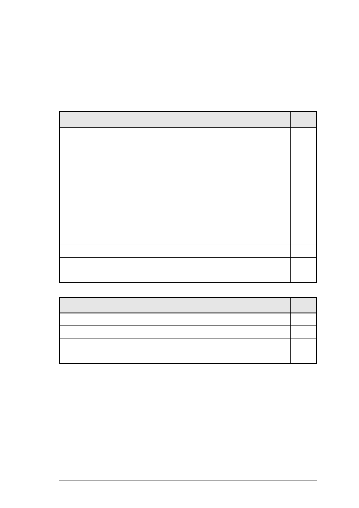
1.2 Specifications
1.2.1 Introduction
The performance figures given are minimum figures, unless otherwise indicated, for
equipment tuned with the maximum switching range and operating at standard room
temperature (+22°C to +28°C) and standard test voltage (13.8V DC).
Where applicable, the test methods used to obtain the following performance figures are
those described in the EIA and ETS specifications. However, there are several parame-
ters for which performance according to the CEPT specification is given. Refer to Sec-
tion 1.2.6 for details of test standards.
Details of test methods and the conditions which apply for Type Approval testing in all
countries can be obtained from Tait Electronics Ltd.
The terms "wide bandwidth", "mid bandwidth" and "narrow bandwidth" used in this
and following sections are defined in the following table.
1.2.2 General
Number Of Channels .. 128 (standard)1
Supply Voltage:
Operating Voltage .. 10.8 to 16V DC
Standard Test Voltage .. 13.8V DC
Polarity .. negative earth only
Polarity Protection .. crowbar diode
Line Keying Supply (if required) .. -50V DC
Supply Current:
Transmit - T836 .. 4.5A (typical)
- T837 .. 600mA
Standby .. 150mA (typical)
Operating Temperature Range .. -30°C to +60°C
Channel Spacing Modulation
100% Deviation Receiver
IF Bandwidth
Wide Bandwidth 25kHz ±5.0kHz 15.0kHz
Mid Bandwidth 20kHz ±4.0kHz 12.0kHz
Narrow Bandwidth 12.5kHz ±2.5kHz 7.5kHz
1. Additional channels may be factory programmed. Contact your nearest Tait Dealer or
Customer Service Organisation.

M830-00
T836/837 General Information
C1.9
Copyright TEL 23/07/99
Dimensions:
Height .. 183mm
Width .. 60mm
Length .. 320mm
Weight .. 2.1kg
Time-Out Timer (optional) .. 0 to 5 minutes1 adjustable in 10 sec-
ond steps
Tail Timer .. 0 to 5 seconds adjustable in 100ms2
steps
Transmit Key Time .. <30ms
Transmit Lockout Timer .. 0 to 1 minute adjustable in 10 second
steps
1.2.3 RF Section
Frequency Range .. 136-174MHz (refer to Section 1.4 and
Section 1.5)
Modulation Type .. FM
Frequency Increment .. 5 or 6.25kHz
Switching Range .. 8MHz (i.e. ±4MHz from the centre
frequency)
Load Impedance .. 50 ohms
Frequency Stability .. ±2.5ppm, -30°C to +60°C
(see also Section 1.4 and Section 1.5)
Adjacent Channel Power (full deviation):
Wide Bandwidth (WB) .. -75dBc
(±25kHz/15kHz B/W)
Mid Bandwidth (MB) .. -70dBc
(±20kHz/12kHz B/W)
Narrow Bandwidth (NB) .. -65dBc
(±12.5kHz/7.5kHz B/W)
Transmitter Side Band Noise:
(no modulation, 15kHz bandwidth)
At ±25kHz .. -95dBc
At ±1MHz .. -105dBc
1. Adjustable from 0 to 10 minutes in PGM800Win version 2.12 and later.
2. Adjustable in 20ms steps in PGM800Win version 2.12 and later.

C1.10
T836/837 General Information
M830-00
23/07/99 Copyright TEL
Intermodulation .. -40dBc with interfering signal of
-30dBc
.. -70dBc with 25dB isolation
& interfering signal of -30dBc
(PA with output isolator)
T836 Mismatch Capability:
Ruggedness .. refer to your nearest Tait Dealer or
Customer Service Organisation
Stability .. 3:1 VSWR (all phase angles)
Radiated Spurious Emissions:
Transmit .. -36dBm to 1GHz
-30dBm to 4GHz
Standby .. -57dBm to 1GHz
-47dBm to 4GHz
Conducted Spurious Emissions: (T836 Only)
Transmit .. -36dBm to 1GHz
-30dBm to 4GHz
Standby .. -57dBm to 1GHz
-47dBm to 4GHz
Power Output:
T836 - Rated Power .. 25W
- Range Of Adjustment .. 5-25W
T837 .. 800mW ±200mW
Duty Cycle (T836 Only) .. 100% @ 25W at +25°C
.. 30% @ 25W at +60°C
.. 100% @ 10W at +60°C
1.2.4 Audio Processor
1.2.4.1 Inputs
Inputs Available .. line, microphone and CTCSS
Line Input:
Impedance .. 600 ohms (balanced)
Sensitivity (60% modulation @ 1kHz)-
With Compressor .. -50dBm
Without Compressor .. -30dBm
Microphone Input:
Impedance .. 600 ohms
Sensitivity (60% modulation @ 1kHz)-
With Compressor .. -70dBm
Without Compressor .. -50dBm

M830-00
T836/837 General Information
C1.11
Copyright TEL 23/07/99
1.2.4.2 Modulation Characteristics
Frequency Response .. flat or pre-emphasised (optional)
(below limiting)
Line And Microphone Inputs:
Pre-emphasised Response-
Bandwidth .. 300Hz to 3kHz (WB & MB)
.. 300Hz to 2.55kHz (NB)
Below Limiting .. within +1, -3dB of a 6dB/octave
pre-emphasis characteristic
Flat Response .. within +1, -2dB of output at 1kHz
Above Limiting Response .. within +1, -2dB of a flat response
(ref. 1kHz)
Distortion .. 2%
Hum And Noise:
Wide Bandwidth .. -55dB (300Hz to 3kHz [EIA]) typical
Mid Bandwidth .. -54dB (CEPT)
Narrow Bandwidth .. -50dB (CEPT)
Compressor (optional):
Attack Time .. 10ms
Decay Time .. 800ms
Range .. 50dB
1.2.4.3 CTCSS
Standard Tones .. all 37 EIA group A, B and C tones
plus 13 commonly used tones
Frequency Error .. 0.08% max.
(from EIA tones)
Generated Tone Distortion .. 1.2% max.
Generated Tone Flatness .. flat across 67 to 250.3Hz to within 1dB
Modulation Level .. adjustable
Modulated Distortion .. <5%
1.2.5 Microcontroller
Auxiliary Ports:
Open Drain Type .. capable of sinking 2.25mA via 2k2Ω
Vds max. .. 5V

C1.12
T836/837 General Information
M830-00
30/04/98 Copyright TEL
1.2.6 Test Standards
Where applicable, this equipment is tested in accordance with the following standards.
1.2.6.1 European Telecommunication Standard
ETS 300 086 January 1991
Radio equipment and systems; land mobile service; technical characteristics and test
conditions for radio equipment with an internal or external RF connector intended pri-
marily for analogue speech.
ETS 300 113 March 1996
Radio equipment and systems; land mobile service; technical characteristics and test
conditions for radio equipment intended for the transmission of data (and speech) and
having an antenna connector.
ETS 300 219 October 1993
Radio equipment and systems; land mobile service; technical characteristics and test
conditions for radio equipment transmitting signals to initiate a specific response in the
receiver.
ETS 300 279 February 1996
Radio equipment and systems; electromagnetic compatibility (EMC) standard for pri-
vate land mobile radio (PMR) and ancillary equipment (speech and/or non-speech).
1.2.6.2 DTI CEPT Recommendation T/R-24-01
Annex I: 1988
Technical characteristics and test conditions for radio equipment in the land mobile
service intended primarily for analogue speech.
Annex II: 1988
Technical characteristics of radio equipment in the land mobile service with regard to
quality and stability of transmission.
1.2.6.3 Telecommunications Industry Association
ANSI/TIA/EIA-603-1992
Land mobile FM or PM communications equipment measurement and performance
standards.

M830-00
T836/837 General Information
C1.13
Copyright TEL 23/07/99
1.3 Product Codes
The three groups of digits in the T830 Series II product code provide information about
the model, type and options fitted, according to the conventions described below.
The following explanation of T830 Series II product codes is not intended to suggest that
any combination of features is necessarily available in any one product. Consult your
nearest Tait Dealer or Customer Service Organisation for more information regarding
the availability of specific models, types and options.
Model
The Model group indicates the basic function of the product, as follows:
T83X-XX-XXXX T835 receiver
T836 25W transmitter
T837 exciter
T838 50W power amplifier
T839 100W power amplifier
Type
The Type group uses two digits to indicate the basic RF configuration of the product.
The first digit in the Type group designates the frequency range:
T83X-XX-XXXX ’1’ for 136-156MHz
’2’ for 148-174MHz
The second digit in the Type group indicates the channel spacing:
T83X-XX-XXXX ’0’ for wide bandwidth (25kHz)
’3’ for mid bandwidth (20kHz)
’5’ for narrow bandwidth (12.5kHz)
Options
T83X-XX-XXXX The Options group uses four digits and/or letters to indicate
any options that may be fitted to the product. This includes
standard options and special options for specific customers.
’0000’ indicates a standard Tait product with no options fitted.
The large number of options precludes listing them here.
C1.14
T836/837 General Information
M830-00
23/07/99 Copyright TEL
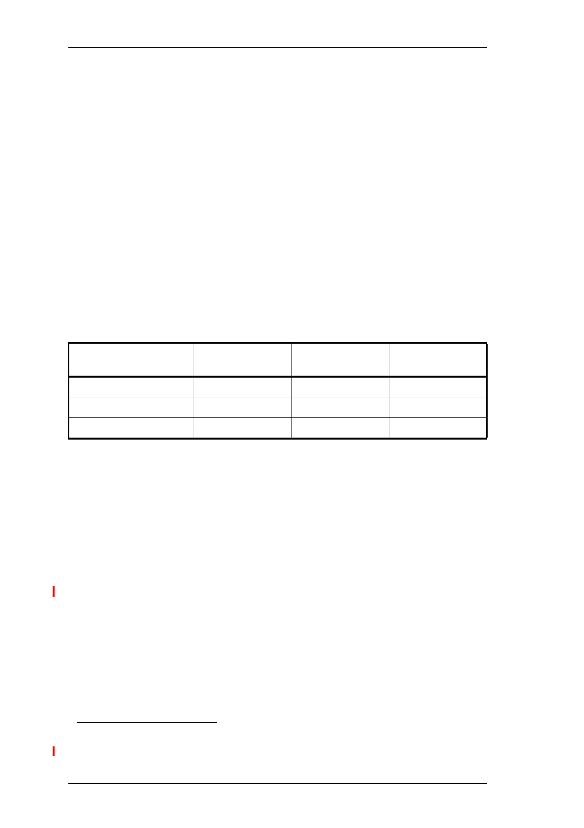
1.4 T836 Standard Product Range
The following table lists the range of standard T836 types (i.e. no options fitted) availa-
ble at the time this manual was published. Consult your nearest Tait Dealer or Cus-
tomer Service Organisation for more information.
You can identify the transmitter type by checking the product code printed on a label on
the rear of the chassis (Figure 1.1 in Part A shows typical labels). You can further verify
the transmitter type by checking the placement of an SMD resistor in the table that is
screen printed onto the PCB (refer to Section 6.1 for more details).
Frequency Range (MHz) 136-156
Deviation (kHz) 2.5 2.5 4 5
TCXOa
a. A TCXO with a stability of ±1ppm (0°C to +60°C) is available to suit specific
requirements. Contact your nearest authorised Tait Dealer or Customer
Service Organisation for further details.
±2.5ppm -30°C to +60°C • •••
Transmitter Type: T836- 16-0000b
b. United States market only.
15-0000 13-0000 10-0000
Frequency Range (MHz) 148-174
Deviation (kHz) 2.5 2.5 4 5
TCXOa±2.5ppm -30°C to +60°C • •••
Transmitter Type: T836- 26-0000b25-0000 23-0000 20-0000
M830-00
T836/837 General Information
C1.15
Copyright TEL 23/07/99
1.5 T837 Standard Product Range
The following table lists the range of standard T837 types (i.e. no options fitted) availa-
ble at the time this manual was published. Consult your nearest Tait Dealer or Cus-
tomer Service Organisation for more information.
You can identify the exciter type by checking the product code printed on a label on the
rear of the chassis (Figure 1.1 in Part A shows typical labels). You can further verify the
exciter type by checking the placement of an SMD resistor in the table that is screen
printed onto the PCB (refer to Section 6.1 for more details).
Frequency Range (MHz) 136-156
Deviation (kHz) 2.5 2.5 4 5
TCXOa
a. A TCXO with a stability of ±1ppm (0°C to +60°C) is available to suit specific
requirements. Contact your nearest authorised Tait Dealer or Customer
Service Organisation for further details.
±2.5ppm -30°C to +60°C • •••
Exciter Type: T837- 16-0000b
b. United States market only.
15-0000 13-0000 10-0000
Frequency Range (MHz) 148-174
Deviation (kHz) 2.5 2.5 4 5
TCXOa±2.5ppm -30°C to +60°C • •••
Exciter Type: T837- 26-0000b25-0000 23-0000 20-0000


M830-00
T836/837 Circuit Operation
C2.1
Copyright TEL 30/04/98
2 T836/837 Circuit Operation
This section provides a basic description of the circuit operation of the T836 transmitter
and T837 exciter.
Note:
Unless otherwise specified, the term "PGM800Win" used in this and follow-
ing sections refers to version 2.00 and later of the software.
Refer to Section 6 where the parts lists, grid reference index and diagrams will provide
detailed information on identifying and locating components and test points on the
main PCB. The parts list and diagrams for the VCO PCB are in Part E.
The following topics are covered in this section.
Section Title Page
2.1 Introduction 2.3
2.2 Microcontroller 2.4
2.3
2.3.1
Synthesised Local Oscillator
Two Point Modulation
2.5
2.6
2.4
2.4.1
VCO
VCO Supply
2.7
2.7
2.5
2.5.1
2.5.2
2.5.3
2.5.4
2.5.5
Audio Processor
General
Audio Inputs
Keying Inputs
Compressor (Automatic Level Control (ALC))
Outputs To Modulators
2.8
2.8
2.8
2.9
2.9
2.9
2.6 Power Supply & Regulator Circuits 2.10
2.7 Transmit Timers 2.11
2.8 T836 Drive Amplifier & PA 2.12
2.9 T837 Exciter Drive Amplifier 2.13

C2.2
T836/837 Circuit Operation
M830-00
30/04/98 Copyright TEL
Figure Title Page
2.1
2.2
2.3
2.4
2.5
2.6
2.7
2.8
T836 High Level Block Diagram
T837 High Level Block Diagram
T836/837 Microcontroller Block Diagram
T836/837 Synthesiser Block Diagram
T836/837 Two Point Modulation
T836/837 Audio Processor Block Diagram
T836/837 Power Supply & Regulators Block Diagram
T836/837 Transmit Timers
2.3
2.3
2.4
2.5
2.6
2.8
2.10
2.11
M830-00
T836/837 Circuit Operation
C2.3
Copyright TEL 30/04/98
2.1 Introduction
The individual circuit blocks which make up the T836 and T837 are:
• synthesiser
•VCO
• audio processor
• drive amplifier
• power amplifier (T836 only)
• voltage regulators.
Each of these circuit blocks is set in its own shielded compartment, formed as an inte-
gral part of the main chassis.
The configuration of the circuit blocks may be seen on a functional level in Figure 2.1
and Figure 2.2. Refer to the circuit diagrams in Section 6.2 (T836) or 6.3 (T837) for more
detail.
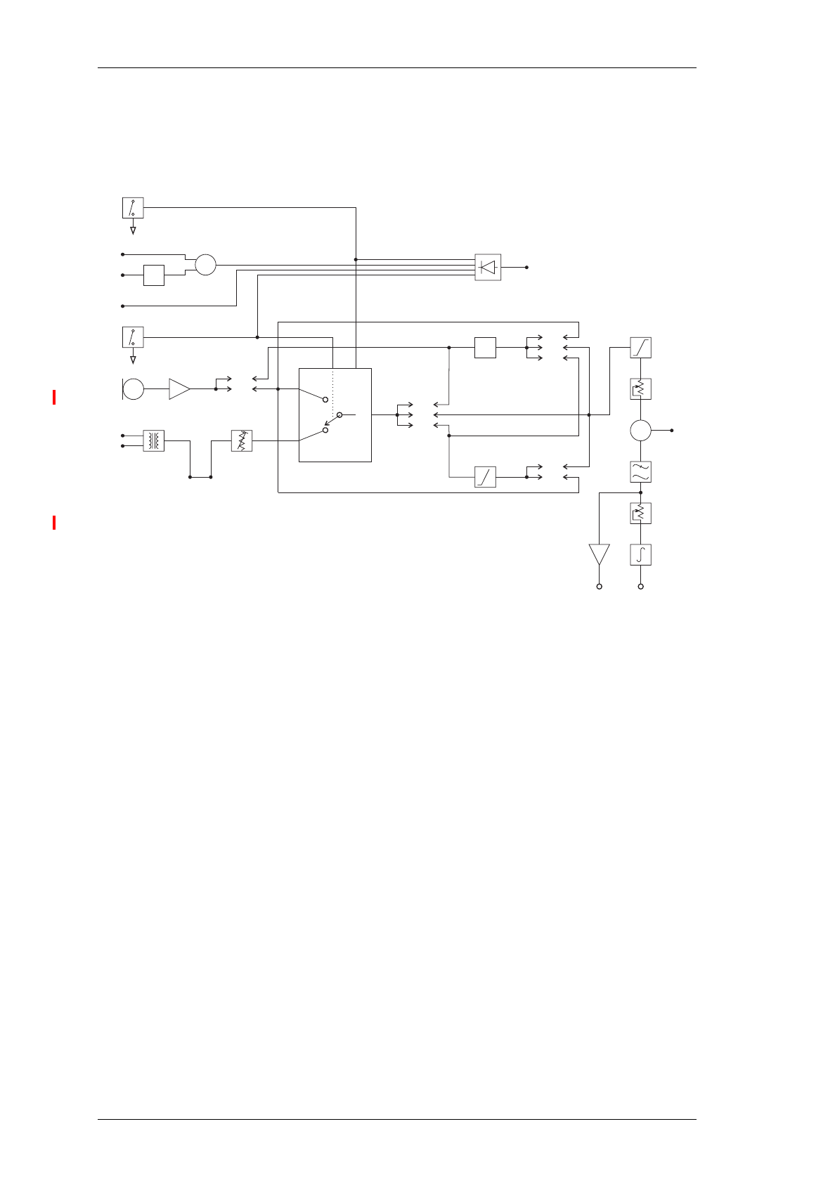
Figure 2.1 T836 High Level Block Diagram
Figure 2.2 T837 High Level Block Diagram
Ramp
Gen.
Time
Delay
Time
Delay
Time
Delay
Audio
Processor
Synthesiser +22dBm
Reference
Oscillator
12.8MHz
Microphone
Line
Transformer
Lock
Detect
PIN
Switch
Power
Control
Drive
Amp. PA
VCO
Gate
Directional
Coupler Low Pass
Filter
Exciter
Output
(+27dBm) Transmitter
Output
(25W)
Tx Reg
&
Audio
Processor
Synthesiser +22dBm
Reference
Oscillator
12.8MHz
Microphone
Line
Transformer
Lock
Detect
PIN
Switch
Switching
Control
Drive
Amp.
Gate
Exciter
Output
(800mW)
&Ramp
Gen.
Tx Reg VCO
Time
Delay
Time
Delay
Low Pass
Filter
PA Control Signal
(via exciter RF coax)
C2.4
T836/837 Circuit Operation
M830-00
23/07/99 Copyright TEL
2.2 Microcontroller
(Refer to the microcontroller circuit diagram (sheet 8) in Section 6.2 or 6.3.)
Figure 2.3 T836/837 Microcontroller Block Diagram
Overall system control of the T836/837 is accomplished by the use of a member of the
80C51 family of microcontrollers (IC810). It runs from internal ROM and RAM, thus
leaving all four ports free for input/output functions.
Non-volatile data storage is achieved by serial communication with a 16kBit EEPROM
(IC820). This serial bus is also used by the microcontroller to program the synthesiser
(IC740) and deviation control EPOTS (IC220).
The main tasks of the microcontroller are as follows:
• program the synthesiser and EPOT;
• interface with the PGM800Win programming software at 9600 baud via the
serial communication lines on D-range 1 (PL100) & D-range 2;
• monitor channel change inputs from D-range 2;
• generate timing waveforms for CTCSS encoding;
• coordinate and implement timing control of the exciter/transmitter;
• control the front panel "Supply" LED (refer to Section 5.3).
5V Reset
5V Digital
Regulator Watchdog
Reset
Channel
Select
Port
Auxiliary
Output
Port
Microcontroller
12.8MHz
Clock
Microcontroller Cavity
CTCSS Tone
External
Serial
Port
EEPROM Synthesiser
Dual Digital
Potentiometer
CTCSS
Encoder
Converter
M830-00
T836/837 Circuit Operation
C2.5
Copyright TEL 30/04/98
2.3 Synthesised Local Oscillator
(Refer to the synthesiser circuit diagram (sheet 7) in Section 6.2 or 6.3 and the VCO cir-
cuit diagram in Part E.)
Figure 2.4 T836/837 Synthesiser Block Diagram
The synthesiser (IC740) employs a phase-locked loop (PLL) to lock a voltage controlled
oscillator (VCO) to a given reference frequency. The synthesiser receives the divider
information from the control microprocessor via a 3 wire serial bus (clock, data, enable).
When the data has been latched in, the synthesiser processes the incoming signals from
the VCO buffer (fin) and the phase modulator (fref).
A reference oscillator at 12.8MHz (IC700) is buffered (IC710 pins 3 & 4) and divided
down to 200kHz (IC730). This 200kHz square wave is then summed with the modulat-
ing audio and passed to an integrator (IC720 pins 9 & 8, Q710, Q720). This produces a
ramping waveform which is centred around a DC level determined by the incoming
audio. IC720 pins 5 & 6 perform as a comparator, ultimately producing a phase-modu-
lated 200kHz square wave. This is followed by another phase shifting stage (IC720 pins
3 & 4, Q730, Q740), before being divided down to 6.25kHz or 5kHz within the synthe-
siser IC (IC740).
A buffered output of the VCO (Q795) is divided with a prescaler and programmable
divider which is incorporated into the synthesiser chip (IC740). This signal is compared
with the phase modulated reference signal at the phase detector (also part of the synthe-
siser chip). The phase detector outputs drive a balanced charge pump circuit (Q760,
Q770, Q775, Q780, Q785) and active loop filter (IC750 pins 5, 6 & 7) which produces a
DC voltage between 0V and 20V to tune the VCO. This VCO control line is further fil-
tered to attenuate noise and other spurious signals. Note that the VCO frequency
increases with increasing control voltage.
If the synthesiser loop loses lock, a pulsed signal appears at LD (pin 2) of IC740. This
signal is filtered and buffered by IC750 pins 1, 2 & 3, producing the Lock-Detect signal
used to shut off the power supply to the drive amplifier. IC750 pin 1 is at 20V when the
synthesiser is out of lock.
/R
Reference
Divider
12.8MHz
Reference
Oscillator Fixed
Divider
/64
Phase
Modulator
Ref
Mod
Phase
Detector Charge
Pump Loop
Filter
FREQUENCY SYNTHESISER IC
Serial
Bus
Clk
Data
En Controller
/N
Programmable
Divider
64/65
Prescaler
VCO PCB
VCO
Modulation
VCO Buffer Output
Buffer
+22dB
m
L.O.
Divider Buffer
f
ref
f
in
Σ
C2.6
T836/837 Circuit Operation
M830-00
23/07/99 Copyright TEL
2.3.1 Two Point Modulation
Frequency modulation occurs by modulating both the VCO input and the synthesiser
reference input. This process is called two point modulation and ensures a flat modula-
tion response from 67Hz to 3kHz (2.55kHz for narrow bandwidth).
The PLL has a fast response time, allowing a Tx key-up time of <30ms. Because of this
fast response time the PLL sees lower modulation frequencies superimposed on the
VCO as an error and corrects for it, resulting in no modulation on the carrier. At modu-
lation frequencies greater than 300Hz the loop cannot correct fast enough and modula-
tion is seen on the carrier. The response of the loop to VCO modulation is shown by f2
in Figure 2.5 below.
To achieve low frequency modulation, the reference oscillator is also modulated so that
the phase detector of IC740 detects no frequency error under modulation. Thus, the
synthesiser loop will not attempt to correct for modulation and the audio frequency
response of the transmitter remains unaffected. The response of the loop to reference
frequency modulation is shown by f1 in Figure 2.5.
The reference modulation is controlled by a 256-step 10k electronic potentiometer
(EPOT) which is adjustable via PGM800Win. The EPOT is made up of 256 resistive sec-
tions (representing approximately 39Ω each) which can be individually addressed by
the microcontroller. Each section can be switched in or out of circuit to achieve the
required total resistance, thus giving control of the reference modulation.
Figure 2.5 T836/837 Two Point Modulation
12
ff
TCXO VCO
Deviation
Frequency

M830-00
T836/837 Circuit Operation
C2.7
Copyright TEL 30/04/98
2.4 VCO
(Refer to the VCO circuit diagram in Part E.)
The VCO transistor (Q1) operates in a common source configuration, with an LC tank
circuit coupled between its gate and drain to provide the feedback necessary for oscilla-
tion. The VCO control voltage from the loop filter (IC750 pin 7) is applied to the vari-
caps (D1-D4) to facilitate tuning within an 8MHz band of frequencies. A trimcap (CV1)
is used for coarse tuning of the VCO. The output from the oscillator circuit drives a cas-
code amplifier stage (Q2, Q3) which supplies +10dBm (typically) to a further stage of
amplification, Q5. This is the final amplifier on the VCO PCB, and delivers +22dBm
(typically) to the exciter drive amplifier.
A low level "sniff" is taken from the output of Q3 and used to drive the divider buffer
(Q795) for the synthesiser (IC740).
The VCO operates at the actual output frequency of the exciter, i.e. there are no multi-
plier stages. The VCO is modulated by superimposing the audio signal onto the control
voltage and by phase modulating the reference signal.
2.4.1 VCO Supply
The VCO is supplied from two switched +9V supplies under the control of the Tx-Reg.
supply.
The VCO (Q1) and buffer amplifier (Q2 & Q3) are supplied from one +9V switched sup-
ply by Q540 via the capacitor multiplier (Q550, C550).
The output amplifier is supplied from the other +9V supply by Q520, Q530, and Q510.
A delay circuit holds the VCO on for a short time after the Tx-Reg. supply has been
switched off. This is to allow the RF power circuits (both exciter and PA) to ramp down
in the correct manner before the VCO is switched off.
C2.8
T836/837 Circuit Operation
M830-00
23/07/99 Copyright TEL
2.5 Audio Processor
(Refer to the audio processor circuit diagram (sheet 2) in Section 6.2 or 6.3.)
Figure 2.6 T836/837 Audio Processor Block Diagram
2.5.1 General
The audio processor comprises several link selectable circuit blocks which may be con-
figured in a variety of combinations to suit individual requirements. The pre-emphasis
network and compressor may be linked individually or cascaded between either or both
audio inputs and the limiter.
Refer to Section 3.5.1 for linking details.
2.5.2 Audio Inputs
Two audio inputs are available: one from a 600 ohm balanced (or unbalanced) line, and
the other from a local microphone. The microphone signal is passed first to a pre-ampli-
fier (Q210) and ultimately to a multiplexer (IC240), but in between may pass through
the compressor (depending on the linking details). The line transformer is also con-
nected to the multiplexer and is disabled by the microphone PTT switch.
A third input for external CTCSS tones is also provided.
Pre-
emphasis
34
6
B
C
5
6
4
34
2
5
3
3
5
7
12
8
N
H
M
I
E
L
J
D
4
6
1
mic.
line
Multiplexer
Inputs
Output
Output
Inhibit
Audio 1 Audio 2
Compressor
Link
Link
Link
Tx Enable
Σ
Carrier
Opto-Key
Tx Key
PTT
Microphone
Input
Line Input
Microphone
Pre-amp.
Opto-coupler
Link
PL205
PL215
PL220
PL210
Limiter
Set Deviation
CTCSS
Low Pass
Filter
Ref. Mod. Adjust
Integrator
Digital Pot. (EPOT)
Digital Pot. (EPOT)
Buffer
Output
To VCO Ref.
Mod.
Constant Current Sink
+
_

M830-00
T836/837 Circuit Operation
C2.9
Copyright TEL 23/07/99
2.5.3 Keying Inputs
There are four ways to key the exciter:
• pulling the Tx-Key line low (pin 13 on D-range 1 [PL100]) at the rear of the set);
• pushing the "Carrier" button on the front panel - this will inhibit all audio;
• using the PTT button on the local microphone, disabling audio from the line;
• via the opto-key inputs (pins 11 and 12 on D-range 1 [PL100]) when electrical
isolation is required. This features a constant current sink (Q270) to ensure reli-
able activation of the opto-coupler (IC250) at low keying voltages.
2.5.4 Compressor (Automatic Level Control (ALC))
The input signal is fed via a current controlled attenuator (Q230, Q220) to a high gain
stage (IC230) from which the output signal is taken. This signal is passed to a compara-
tor (IC230) which toggles whenever the audio signal exceeds a DC threshold deter-
mined by RV220. Thus, the comparator produces a square wave whose mark-space
ratio is determined by the amplitude of the audio signal. This square wave pumps up
the reservoir capacitor (C233) which controls the attenuator (Q230, Q220), thus complet-
ing the feedback loop.
The compression level is set by adjustment of the comparator threshold (RV220).
Note:
Although the high dynamic range of the compressor allows the use of very
low audio signal levels, such conditions will be accompanied by a degrada-
tion of the signal-to-noise ratio. Very low audio input levels should there-
fore be avoided where possible.
2.5.5 Outputs To Modulators
The output signal from the limiter (IC210, IC230) is added with a CTCSS tone at a sum-
ming amplifier (IC260). The signal is then low pass filtered (IC260) and split to supply
the two modulators.
Since the VCO modulator is a true frequency modulator, its audio is simply buffered
(IC260). The reference modulator, however, is a phase modulator and its audio must
first be integrated (IC210).
It is vital that the audio levels to the modulators are accurately set, relative to each
other. Hence the inclusion of level adjustment in the reference modulator path. Once
set, adjustments to absolute deviation may be made only by IC220, a 256-step 10k elec-
tronic potentiometer (EPOT), which is controlled via PGM800Win. The EPOT is made
up of 256 resistive sections (representing approximately 39Ω each) which can be indi-
vidually addressed by the microcontroller. Each section can be switched in or out of cir-
cuit to achieve the required total resistance, thus adjusting the absolute deviation level.
C2.10
T836/837 Circuit Operation
M830-00
23/07/99 Copyright TEL
2.6 Power Supply & Regulator Circuits
(Refer to the regulators circuit diagram (sheet 6) in Section 6.2 or 6.3.)
Figure 2.7 T836/837 Power Supply & Regulators Block Diagram
The T836 and T837 are designed to operate from a 10.8-16V DC supply (13.8V nominal).
A 5.3V regulator (IC630) runs directly from the 13.8V rail, driving much of the synthe-
siser circuitry. It is also used as the reference for a DC amplifier (IC640, Q630, Q620)
which provides a medium current capability 9V supply.
A switching power supply (Q660, Q670) runs from the 9V supply and provides a low
current capability +20V supply. This is used to drive the synthesiser loop filter (IC750),
giving a VCO control voltage range of up to 20V, and the Lock-Detect amplifiers.
Ultimate control of the transmitter is via the Tx-Reg. supply, switched from 9V by Q610.
This is enabled via the Tx-Enable signal from the audio processor, and microprocessor.
A crowbar diode is fitted for protection against connection to a power supply of incor-
rect polarity. It also provides transient overvoltage protection.
Note:
A fuse must be fitted in the power supply line for the diode to provide effec-
tive protection.
Crowbar
Diode LVI
5V
Reg
DC
Amp Switching
PS 5V Dig
Reg
Power
Switch
13.8V
Nom. 5V 5V Dig9V 20V
13.8V Nom.
From Rear
D-Range
Tx Enable
Buffer
Tx Reg.
+9V
µP
Watchdog
Timer
Micro-
controller
µP
Reset
M830-00
T836/837 Circuit Operation
C2.11
Copyright TEL 23/07/99
2.7 Transmit Timers
The transmit tail timer, transmit timeout timer and transmit lockout timer can all be set
from PGM800Win. The fields for setting these are found on the system information
page. These three timers operate as follows (refer also to Figure 2.8):
Figure 2.8 T836/837 Transmit Timers
Timer Function Adjustment
Transmit Tail Sets the tail time during which the
transmitter stays keyed after the exter-
nal key source has been removed.
0-5 seconds in 100ms
stepsa
a. Adjustable in 20ms steps in PGM800Win version 2.12 and later.
Transmit Timeout Sets the maximum continuous trans-
mission time. Once the timer has
timed out, the transmitter must be
keyed again, unless prevented by the
transmit lockout timer.
0-300 secondsb in 10
second steps
b. Adjustable from 0 to 600 seconds in PGM800Win version 2.12 and later.
Transmit Lockout Sets the period of time that must
elapse after a timeout before the trans-
mitter can re-transmit. Once the timer
has timed out, the transmitter can be
keyed again.
0-60 seconds in 10
second steps
On
Lockout Time
Timeout
Time
On
Tail Time
Tx-Enable
Tx-Reg.
Tx-Enable
Tx-Reg.

C2.12
T836/837 Circuit Operation
M830-00
30/04/98 Copyright TEL
2.8 T836 Drive Amplifier & PA
(Refer to Figure 2.1 and the exciter and PA circuit diagrams (sheets 3 & 4) in Section 6.2.)
The output power of the PA is maintained at a constant level via a power control loop
applied to the two-stage, wide band exciter amplifier (Q365, Q370). The forward and
reverse RF power levels are sensed via a dual directional coupler and detector diodes
(D410, D420 in the PA cavity). The detected DC signals are summed with the ’power
adjust’ level and fed to the control integrator (IC330 pins 1, 2 & 3). The output control
voltage is buffered by Q310 and Q315, and applied to the collectors of the wide band
exciter amplifier.
Note:
Forward and reflected power signals are summed so that, under high
VSWR, the power control will turn the output RF level down.
To reduce the spurious output level when the synthesiser is out-of-lock, the Tx-Reg. and
Lock-Detect signals are gated to inhibit the PA control circuit and to switch off the RF
signal at the input to the drive amplifier. This is achieved by a PIN switch attenuator
(D340, D350, D360).
Cyclic keying control is provided by additional circuitry consisting of several time
delay, ramp and gate stages:
• Q350, Q355, Q360, IC330 pins 1, 2 & 3 power ramping
• Q340, Q345 Tx-Reg. and Lock-Detect gate
• Q320, Q325, Q330, Q335 delay and PIN switch drive.
This is to allow the RF power circuits (both exciter and PA) to ramp up and down in a
controlled manner so that minimal adjacent channel interference is generated during
the transition.
The output of the wide band amplifier is approximately 500mW (+27dBm) for an input
of 170mW (+22dBm) when the power control is set to maximum.
The zener diode (D330) limits the upper range of the controlled voltage to the exciter
transistors.
A temperature sensor (R460) is provided so that the RF output power can be reduced to
a preset level when a set temperature is exceeded. This is a protection circuit (IC330
pins 5, 6 & 7, Q305) to prevent overheating, as the unit is not rated for continuous oper-
ation at high temperatures (refer to Section 1.2.3 for duty cycle specifications). RV330
sets the PA output power while under high temperature fold-back conditions.
R359, R360 and R362 form a 6dB attenuator to provide good VCO/exciter isolation.
The output attenuator (R392, R390, R394 and R396) aids in reducing exciter/PA interac-
tion while also ensuring a reasonable match for Q350.
The RF output from the exciter is fed to the driver stage (Q415) and then to the final
(Q425). DC is fed to the final via a low pass filter with special low frequency decou-
pling. CV451 tunes the output matching across the entire band.

M830-00
T836/837 Circuit Operation
C2.13
Copyright TEL 30/04/98
2.9 T837 Exciter Drive Amplifier
(Refer to Figure 2.2 and the exciter circuit diagram (sheet 3) in Section 6.3.)
A two-stage, wide band amplifier (Q365, Q370) provides an output level of approxi-
mately 800mW (+29dBm) for an input of 170mW (+22dBm) from the VCO. IC330 pins
5, 6 & 7, Q310, and Q315 provide a 10.5V regulated supply for the exciter.
To reduce the spurious output level when the synthesiser is out-of-lock, the Tx-Reg. and
Lock-Detect signals are gated to inhibit the exciter control circuit and to switch off the
RF signal at the input to the drive amplifier. This is achieved by a PIN switch attenuator
(D340, D350, D360).
Cyclic keying control is provided by additional circuitry consisting of several time
delay, ramp and gate stages:
• Q305, IC330 pins 5, 6 & 7 power ramping
• Q340, Q345 Tx-Reg. and Lock-Detect gate
• Q320, Q325, Q330, Q335 delay and PIN switch drive.
This is to allow the RF power circuits (both exciter and PA) to ramp up and down in a
controlled manner so that minimal adjacent channel interference is generated during
the transition.
R359, R360 and R362 form a 6dB attenuator to provide good VCO/drive amplifier isola-
tion.
The output attenuator (R392, R390, R394, R396) assists in reducing exciter/PA interac-
tion while also ensuring a good match for Q370.
Note:
The exciter provides a DC control signal to the PA via the RF coax. This is
injected via L390.


M830-00
T836/837 Initial Tuning & Adjustment
C3.1
Copyright TEL 23/07/99
3 T836/837 Initial Tuning & Adjustment
Caution:
This equipment contains CMOS devices which are susceptible to dam-
age from static charges. Refer to Section 1.2 in Part A for more infor-
mation on anti-static procedures when handling these devices.
The following section describes both short and full tuning and adjustment procedures
and provides information on:
• channel programming
• selecting required audio links
• synthesiser alignment
• PA alignment (T836 only)
• modulator adjustment
• limiter adjustment
• setting line level
• compressor adjustment
• timer adjustment.
Note:
Unless otherwise specified, the term "PGM800Win" used in this and follow-
ing sections refers to version 2.00 and later of the software.
Refer to Figure 4.4 and Figure 4.5 which show the location of the main tuning and
adjustment controls. Refer also to Section 6 where the parts lists, grid reference index
and diagrams will provide detailed information on identifying and locating compo-
nents and test points on the main PCB. The parts list and diagrams for the VCO PCB are
in Part E.
Section Title Page
3.1 Introduction 3.3
3.2 Channel Programming 3.3
3.3 Test Equipment Required 3.4
3.4
3.4.1
3.4.2
3.4.3
3.4.4
3.4.5
3.4.6
3.4.7
Short Tuning Procedure
Introduction
Synthesiser Alignment
Output Power Adjustment (T836 Only)
Two Point Modulation Adjustment
CTCSS Encoder (If Used)
FM Deviation (Limiter) Adjustment
Line-in Level Adjustment
3.5
3.5
3.5
3.5
3.6
3.7
3.7
3.7

C3.2
T836/837 Initial Tuning & Adjustment
M830-00
23/07/99 Copyright TEL
3.5
3.5.1
3.5.2
Audio Processor Links
Link Details
Typical Options
3.8
3.8
3.8
3.6 Synthesiser Alignment 3.9
3.7 PA Alignment (T836 Only) 3.10
3.8 Thermal Shutdown (T836 Only) 3.10
3.9
3.9.1
3.9.2
3.9.3
3.9.4
3.9.5
3.9.6
3.9.6.1
3.9.6.2
3.9.6.3
Audio Processor
Two Point Modulation
Modulator Adjustment
CTCSS Encoder (If Used)
Limiter Adjustment
Line Level Without Compressor
Compressor
Compressor On Line Input Only
Compressor On Microphone Input Only
Compressor On Both Line & Microphone Inputs
3.11
3.11
3.11
3.12
3.12
3.12
3.13
3.13
3.13
3.14
Figure Title Page
3.1
3.2
T836/837 Test Equipment Set-up With T800-01-0010
T836/837 Test Equipment Set-up Without T800-01-0010
3.4
3.4
Section Title Page

M830-00
T836/837 Initial Tuning & Adjustment
C3.3
Copyright TEL 23/07/99
3.1 Introduction
When you receive your T836 transmitter or T837 exciter it will be run up and working
on a particular frequency (the "default channel")1. If you want to switch to a frequency
that is within the 8MHz switching range (i.e. ±4MHz from the factory programmed fre-
quency), you should only need to reprogram the transmitter/exciter with the
PGM800Win software (refer to the PGM800Win programming kit and Section 3.2
below).
However, if you want to switch to a frequency outside the 8MHz switching range, you
will have to reprogram and re-tune the transmitter/exciter to ensure correct operation.
In this case you should carry out the short tuning procedure described in Section 3.4.
If you have carried out repairs or other major adjustments, you must carry out the full
tuning and adjustment procedure described in this section (except for Section 3.4).
3.2 Channel Programming
You can program up to 128 channel frequencies into the transmitter/exciter’s EEPROM
memory (IC820) by using the PGM800Win software package and an IBM PC. You can
also use PGM800Win to select the transmitter/exciter’s current operating frequency (or
"default channel").
If the transmitter/exciter is installed in a rack frame, you can program it via the pro-
gramming port in the speaker panel. However, you can also program the transmitter/
exciter before it is installed in a rack frame as follows:
• by using a T800-01-0010 calibration test unit;
• via D-range 1;
• via D-range 2 (standard T800-03-0000 auxiliary D-range only);
• via SK805 (internal Micromatch connector).
If you do not use the T800-01-0010, you will have to connect the PC to the transmitter/
exciter via a module programming interface (such as the T800-01-0004).
For a full description of the channel programming procedure, refer to the PGM800Win
programming software user’s manual.
Note:
When an auxiliary D-range kit (D-range 2 - T800-03-0000) is fitted, you can
also select a channel with an external switch, such as the DIP switch on the
rack frame backplane PCB. Refer to Part C in the T800 Series Ancillary
Equipment Service Manual (M800-00-101 or later issue) or consult your
nearest Tait Dealer or Customer Service Organisation for further details.
1. Use the "Read Module" function in PGM800Win to find out what the default channel is.
C3.4
T836/837 Initial Tuning & Adjustment
M830-00
23/07/99 Copyright TEL
3.3 Test Equipment Required
You will need the following test equipment:
• computer with PGM800Win installed
• T800 programming kit
• module programming interface (e.g. T800-01-0004 - optional)
• 13.8V power supply
• digital multimeter
• audio signal generator
• RF power meter
• audio voltmeter x 2
• modulation meter
• oscilloscope (digital preferred)
• 20dB or 40dB pad
• T800-01-0010 calibration test unit (optional)
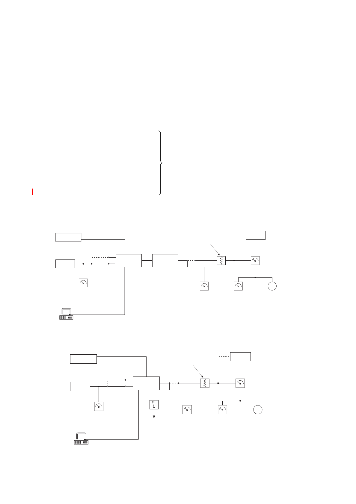
Figure 3.1 and Figure 3.2 show typical test equipment set-ups.
Figure 3.1 T836/837 Test Equipment Set-up With T800-01-0010
Figure 3.2 T836/837 Test Equipment Set-up Without T800-01-0010
or RF test set (optional)
Frequency
Counter
Audio
Voltmeter
RF Power
Meter Oscilloscope
AF O/P
Modulation
Meter
20dB pad: exciter
40dB pad: transmitter
RF O/P
PGM800Win
PSU
+13.8V
-Ve
Audio
Generator
Line I/P
CTCSS I/P
Ω600
Audio
Voltmeter
Exciter/
Transmitter
T800
Calibration
Test Unit
PGM800Win
Serial
Com
PSU
+13.8V
-Ve
Frequency
Counter
Audio
Voltmeter
RF Power
Meter Oscilloscope
AF O/P
Modulation
Meter
20dB pad: exciter
40dB pad: transmitter
Audio
Generator
Line I/P
CTCSS I/P
Ω600
Audio
Voltmeter
Key
RF O/P
Exciter/
Transmitter
via module programming interface
(e.g. T800-01-0004)

M830-00
T836/837 Initial Tuning & Adjustment
C3.5
Copyright TEL 30/04/98
3.4 Short Tuning Procedure
Use this procedure only if you want to reprogram the T836/837 to a frequency outside
the 8MHz switching range and do not intend to carry out any other major adjustments
or repairs.
3.4.1 Introduction
Reprogram the operating frequency as described in the PGM800Win program-
ming kit (refer to Section 3.2).
Remove the top cover (nearest the handle).
Set up the test equipment as described in Section 3.3.
Set the links in the audio processor section as required (refer to Section 3.5).
3.4.2 Synthesiser Alignment
• Connect a high impedance voltmeter to PL4-1 or the junction of L1 & R1 in the
VCO (this measures the synthesiser loop voltage).
• Key the transmitter by earthing the Tx-Key line.
•Single Channel Tune VCO trimmer CV1 for a synthesiser loop voltage of
9V.
Multichannel Tune VCO trimmer CV1 for a synthesiser loop voltage of
9V on the middle channel.
If there is no middle channel, tune CV1 so that the chan-
nels are symmetrically placed around a loop voltage of 9V.
All channels should lie within the upper and lower limits
of 13V and 5V respectively.
Do not attempt to program channels with a greater fre-
quency separation than the specified switching range of
8MHz.
3.4.3 Output Power Adjustment (T836 Only)
Connect an RF power meter to the output socket and key the transmitter.
Turn RV320 (power adjust) fully clockwise.
Tune CV451 (output power trim) for maximum output power and check that this
is >30W.
Adjust RV320 for the required output power (between 5 and 25W).
Readjust CV451 to reduce the supply current by up to 0.5A.

C3.6
T836/837 Initial Tuning & Adjustment
M830-00
23/07/99 Copyright TEL
3.4.4 Two Point Modulation Adjustment
Note 1:
In this and following sections deviation settings are given first for wide
bandwidth sets, followed by settings in brackets for mid bandwidth sets ( )
and narrow bandwidth sets [ ].
Note 2:
The reference modulation and limiter adjustments are controlled by 256-
step electronic potentiometers (EPOTs), which are adjusted via the “Refer-
ence Modulation” and “Deviation” settings in PGM800Win. This allows the
two point modulation and deviation settings to be adjusted for each chan-
nel.
Note 3:
To optimise the modulation response across the switching range, repeat
steps 1-4 below for each channel that will be used (usually needed only for
data applications). In applications where the modulation response is less
critical (e.g. voice use only), carry out steps 1-4 below on the middle channel
and use the “EPOT Fill” option1 in PGM800Win to copy the value to the
other channels.
1. Inject an audio signal of 600Hz 1.5V rms (+5dBm) into the CTCSS input (D-range
1 (PL100) pin 8).
Key the transmitter by earthing the Tx-Key line.
2. Adjust the output from the audio generator to obtain ±3kHz (±2.4kHz) [±1.5kHz]
deviation at 600Hz.
3. Change the input frequency to 120Hz and, using PGM800Win, adjust the value of
the “Reference Modulation” EPOT setting for the current channel to obtain ±3kHz
(±2.4kHz) [±1.5kHz] deviation (you can use either the mouse or up and down
arrow keys).
4. Change the input frequency back to 600Hz.
Repeat steps 2 and 3 above until the deviations achieved at the two input frequen-
cies are within 0.2dB of each other. You will need to do this at least four times.
5. Sweep the audio between 50 and 300Hz for peaks.
Note:
A peak between 50 and 300Hz will indicate a fault condition, i.e:
- incorrect set-up
or - modulation circuitry fault.
The specification window is ±1dB relative to 150Hz from 65 to 260Hz.
1. Use the “EDIT FILL” button on the tool bar or go to “Edit”, “Fill”, “Epot Settings” on
the menu bar.

M830-00
T836/837 Initial Tuning & Adjustment
C3.7
Copyright TEL 23/07/99
3.4.5 CTCSS Encoder (If Used)
Program a CTCSS tone on the default channel using PGM800Win.
If you are using an RF test set, turn off the 300Hz high pass filter.
Key the T836/837 with the front panel "Carrier" switch.
Adjust RV805 (CTCSS level adjust) to give ±500Hz (±350Hz) [±250Hz] deviation.
Set the maximum deviation as per Section 3.4.6.
3.4.6 FM Deviation (Limiter) Adjustment
Note:
If the T836/837 will be used over the whole 8MHz switching range, you
must set the deviation for each channel. However, if the module will be
used on frequencies that cover only a 1MHz (or less) switching range, you
can set the deviation on the middle channel and use this value for all other
channels with the “EPOT Fill” option in PGM800Win.
Inject 1kHz at -10dBm into the line input (D-range 1 (PL100) pins 1 & 4; pins 2 & 3
shorted; refer to Section 2.2 of Part F).
Adjust RV210 (line sensitivity) fully clockwise and key the transmitter by earthing
the Tx-Key line. Using PGM800Win, adjust the value of the “Deviation” EPOT
setting for the current channel to obtain a deviation limit of ±4.7kHz (±3.8kHz)
[±2.3kHz] (you can use either the mouse or up and down arrow keys).
Sweep the audio frequency from 100Hz to 4kHz and ensure that the maximum
deviation does not exceed ±4.7kHz (±3.8kHz) [±2.3kHz]. Readjust “Deviation” if
necessary via PGM800Win.
3.4.7 Line-in Level Adjustment
Remove the CTCSS signal (if used).
Set the injected signal at the line input to the required line level (typically -10 to
-20dBm).
Adjust RV210 (line sensitivity) to provide ±3kHz (±2.4kHz) [±1.5kHz] deviation.
Reapply the CTCSS signal (if required).

C3.8
T836/837 Initial Tuning & Adjustment
M830-00
30/04/98 Copyright TEL
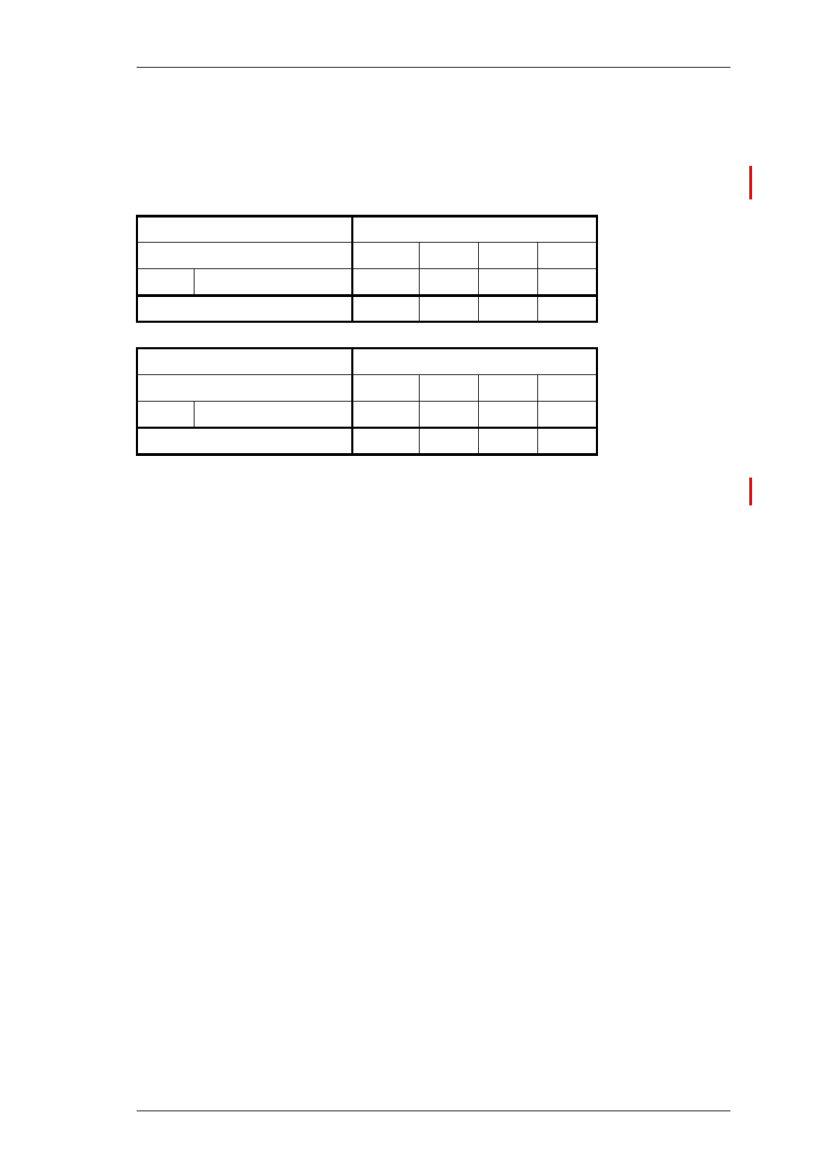
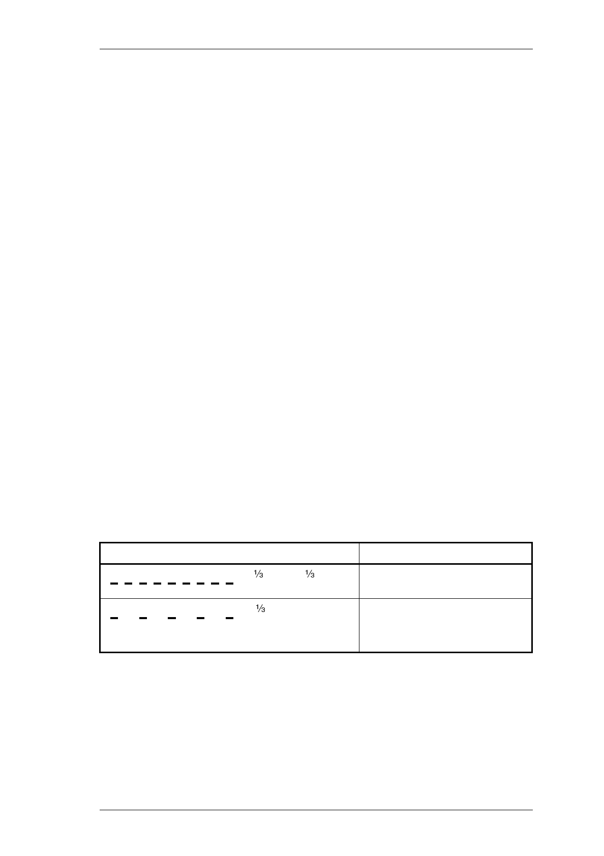
3.5 Audio Processor Links
3.5.1 Link Details
Use the following table to set up the audio processor to the configuration you require.
You should set the audio processor links before carrying out any of the tuning and
adjustment procedures. The factory settings are shown in brackets [ ].
3.5.2 Typical Options
Plug Linka
a. The letters in this column and in the table in Section 3.5.2 below refer to the identification
letters screen printed onto the PCB beside each pair of pins.
Function
PL205
1-2
[3-4]
5-6
A
B
C
not connected
microphone pre-amp. output to compressor input
microphone pre-amp. output to multiplexer input
PL210
[1-2]
3-4
5-6
L
M
N
multiplexer output to pre-emphasis input
multiplexer output to limiter input
multiplexer output to compressor input
PL215
1-2
[3-4]
5-6
7-8
9-10
G
H
I
J
K
not connected
compressor output to multiplexer input
compressor output to limiter input
compressor output to pre-emphasis input
not connected
PL220
1-2
[3-4]
5-6
D
E
F
pre-emphasis output to multiplexer input
pre-emphasis output to limiter input
not connected
PL205 PL210 PL215 PL220
microphone pre-amp. compressed
and pre-emphasised;
line input pre-emphasised
(standard set-up)
[3-4]
B
[1-2]
L
[3-4]
H
[3-4]
E
microphone pre-amp. compressed
and pre-emphasised;
line input unprocessed
3-4
B
3-4
M
7-8
J
1-2
D
line and microphone compressed
and pre-emphasised
5-6
C
5-6
N
7-8
J
3-4
E
microphone pre-amp. compressed;
line and microphone flat response
3-4
B
3-4
M
3-4
H
5-6
F

M830-00
T836/837 Initial Tuning & Adjustment
C3.9
Copyright TEL 23/07/99
3.6 Synthesiser Alignment
• Ensure that the T836/837 has been programmed with the required frequencies
using PGM800Win software.
•Single Channel Select a channel using PGM800Win.
Multichannel Select the middle channel via PGM800Win.
• Connect a high impedance voltmeter to PL4-1 or the junction of L1 and R1 in the
VCO (this measures the synthesiser loop voltage).
• Key the transmitter by earthing the Tx-Key line.
Single Channel Tune VCO trimmer CV1 for a synthesiser loop voltage of
9V.
Multichannel Tune VCO trimmer CV1 for a synthesiser loop voltage of
9V on the middle channel.
If there is no middle channel, tune CV1 so that the chan-
nels are symmetrically placed around a loop voltage of 9V.
All channels should lie within the upper and lower limits
of 13V and 5V respectively.
Do not attempt to program channels with a greater fre-
quency separation than the specified switching range
(8MHz).
• Check that the exciter output power is:
T836 500mW +200, -100mW (measured at SK310 in the exciter section)
T837 800mW ±200mW (measured at the rear panel N-type connector).
• Measure the exciter output frequency and adjust the TCXO (=IC700) trimmer if
required.
Caution:
This trimmer is susceptible to physical damage. Do not exert a down-
ward force of more than 500g (1lb) when adjusting.

C3.10
T836/837 Initial Tuning & Adjustment
M830-00
30/04/98 Copyright TEL
3.7 PA Alignment (T836 Only)
Check that the exciter is connected to the PA with the coaxial link.
Connect an RF power meter to the PA output.
Turn RV320 (power adjust) fully clockwise.
Measure and record the voltage (VL) at L490; perform this measurement at room
temperature so that the NTC (R460) is close to 25°C.
Key the transmitter by earthing the Tx-Key line.
Tune CV451 until maximum power is obtained.
Reduce the current by approximately 1A by detuning CV451 or until the power
drops below 30W.
Check that the total current drawn is less than 4.5A for 25W output power.
Adjust RV320 for an output power between 5 and 25W.
3.8 Thermal Shutdown (T836 Only)
Key the transmitter by earthing the Tx-Key line and set the output power to 25W
as described in Section 3.7.
Short L490 to ground.
Set RV330 (high temperature power adjust) for an output power of 5W.
Set RV310 (temperature adjust) to 0.16VL volts (measured at IC330 pin 5), where
VL is the voltage measured at L490 in Section 3.7. This sets the thermal shutdown
at 85°C at NTC R460.

M830-00
T836/837 Initial Tuning & Adjustment
C3.11
Copyright TEL 23/07/99
3.9 Audio Processor & CTCSS
3.9.1 Two Point Modulation
The T836 and T837 utilise two point modulation to obtain a wide audio bandwidth
independent of the synthesiser loop filter response. This is achieved by simultaneously
frequency modulating the VCO and phase modulating the synthesiser reference fre-
quency. The relative signal levels fed to the two modulators are quite critical and cause
interaction when setting up.
Both modulating signals require readjustment when the exciter is shifted in frequency
greater than the switching range (i.e. ∆F>±4MHz).
Note 1:
In this and following sections deviation settings are given first for wide
bandwidth sets, followed by settings in brackets for mid bandwidth sets ( )
and narrow bandwidth sets [ ].
Note 2:
The reference modulation and limiter adjustments are controlled by 256-
step electronic potentiometers (EPOTs), which are adjusted via the “Refer-
ence Modulation” and “Deviation” settings in PGM800Win. This allows the
two point modulation and deviation settings to be adjusted for each chan-
nel.
Note 3:
To optimise the modulation response across the switching range, repeat
steps 1-4 below for each channel that will be used (usually needed only for
data applications). In applications where the modulation response is less
critical (e.g. voice use only), carry out steps 1-4 below on the middle channel
and use the “EPOT Fill” option1 in PGM800Win to copy the value to the
other channels.
3.9.2 Modulator Adjustment
1. Inject an audio signal of 600Hz 1.5V rms (+5dBm) into the CTCSS input (D-range
1 (PL100) pin 8).
Key the transmitter by earthing the Tx-Key line.
2. Adjust the output from the audio generator to obtain ±3kHz (±2.4kHz) [±1.5kHz]
deviation at 600Hz.
3. Change the input frequency to 120Hz and, using PGM800Win, adjust the value of
the “Reference Modulation” EPOT setting for the current channel to obtain ±3kHz
(±2.4kHz) [±1.5kHz] deviation (you can use either the mouse or up and down
arrow keys).
4. Change the input frequency back to 600Hz.
Repeat steps 2 and 3 above until the deviations achieved at the two input frequen-
cies are within 0.2dB of each other. You will need to do this at least four times.
1. Use the “EDIT FILL” button on the tool bar or go to “Edit”, “Fill”, “Epot Settings” on
the menu bar.

C3.12
T836/837 Initial Tuning & Adjustment
M830-00
23/07/99 Copyright TEL
5. Sweep the audio between 50 and 300Hz for peaks.
Note:
A peak between 50 and 300Hz will indicate a fault condition, i.e:
- incorrect set-up
or - modulation circuitry fault.
The specification window is ±1dB relative to 150Hz from 65 to 260Hz.
3.9.3 CTCSS Encoder (If Used)
Program a CTCSS tone on the default channel using PGM800Win.
If you are using an RF test set, turn off the 300Hz high pass filter.
Key the T836/837 with the front panel "Carrier" switch.
Adjust RV805 (CTCSS level adjust) to give ±500Hz (±350Hz) [±250Hz] deviation.
Set the maximum deviation as per Section 3.9.4.
3.9.4 Limiter Adjustment
Note:
If the T836/837 will be used over the whole 8MHz switching range, you
must set the deviation for each channel. However, if the module will be
used on frequencies that cover only a 1MHz (or less) switching range, you
can set the deviation on the middle channel and use this value for all other
channels with the “EPOT Fill” option in PGM800Win.
Set the links in the audio processor section as required (refer to Section 3.5).
Inject 1kHz at -10dBm into the line input (D-range 1 (PL100) pins 1 & 4; and pins 2
& 3 shorted; refer to Section 2.2 of Part F).
Adjust RV210 (line sensitivity) fully clockwise and key the transmitter by earthing
the Tx-Key line. Using PGM800Win, adjust the value of the “Deviation” EPOT
setting for the current channel to obtain a deviation limit of ±4.7kHz (±3.8kHz)
[±2.3kHz] (you can use either the mouse or up and down arrow keys).
Sweep the audio frequency from 100Hz to 4kHz and ensure that the maximum
deviation does not exceed ±4.7kHz (±3.8kHz) [±2.3kHz]. Readjust “Deviation” if
necessary via PGM800Win.
3.9.5 Line Level Without Compressor
This section assumes that the compressor is not used. If the compressor is required,
refer to Section 3.9.6.
Remove the CTCSS signal (if used).

M830-00
T836/837 Initial Tuning & Adjustment
C3.13
Copyright TEL 23/07/99
Adjust the line sensitivity as follows:
• set the injected signal at the line input to the required line level (typically -10 to
-20dBm);
• adjust RV210 (line sensitivity) to provide ±3kHz (±2.4kHz) [±1.5kHz] devia-
tion.
Reapply the CTCSS signal (if required).
3.9.6 Compressor
The compressor may be used on the line input only, the microphone input only, or on
both the line and microphone inputs. If the compressor is used, refer to one of the fol-
lowing sections as appropriate.
3.9.6.1 Compressor On Line Input Only
Set RV210 (line sensitivity) fully clockwise and key the transmitter by earthing the
Tx-Key line.
Reduce the line level to -50dBm at 1kHz and set RV220 (compression level) fully
clockwise.
Check that ±3kHz (±2.4kHz) [±1.5kHz] deviation is still available.
Slowly increase the audio input level until the demodulated waveform shows sig-
nificant signs of clipping (approximately ±4.5kHz (±3.6kHz) [±2.3kHz] deviation).
Adjust RV220 anticlockwise until the demodulated waveform is just clipping
(approximately ±4kHz (±3.2kHz) [±2kHz] deviation).
Increase the input level to -10dBm and check that the test tone is still held just into
clipping. The input line level should be typically -10 to -20dBm.
3.9.6.2 Compressor On Microphone Input Only
Key the transmitter by earthing the Tx-Key line and plug a microphone jack into
the front panel socket.
Adjust RV220 (compression level) fully clockwise.
Acoustically couple the microphone to a tone box (1kHz) and close the PTT
switch.
Increase the audio level until the demodulated waveform shows significant signs
of clipping (approximately ±4.5kHz (±3.6kHz) [±2.3kHz] deviation).
Adjust RV220 anticlockwise until the demodulated waveform is just clipping
(approximately ±4kHz (±3.2kHz) [±2kHz] deviation).

C3.14
T836/837 Initial Tuning & Adjustment
M830-00
23/07/99 Copyright TEL
Increase the audio level by 10dB and verify that the test tone is held just into clip-
ping.
Whistle steadily into the microphone, checking that approximately ±4kHz
(±3.2kHz) [±2kHz] deviation is produced. The modulated waveform should be
basically sinusoidal.
Speak into the microphone, checking that the modulation peaks reach about
±5kHz (±4kHz) [±2.5kHz] deviation.
As the line is to be used without compression, set RV210 (line sensitivity) as
described in Section 3.9.5.
3.9.6.3 Compressor On Both Line & Microphone Inputs
Set up as described in Section 3.9.6.1.

M830-00
T836/837 Functional Testing
C4.1
Copyright TEL 23/07/99
4 T836/837 Functional Testing
Caution:
This equipment contains CMOS devices which are susceptible to dam-
age from static charges. Refer to Section 1.2 in Part A for more infor-
mation on anti-static procedures when handling these devices.
The following test procedures will confirm that the T836/837 has been tuned and
adjusted correctly and is fully operational.
Note 1:
In this and following sections deviation settings are given first for wide
bandwidth sets, followed by settings in brackets for mid bandwidth sets ( )
and narrow bandwidth sets [ ].
Note 2:
Unless otherwise specified, the term "PGM800Win" used in this and follow-
ing sections refers to version 2.00 and later of the software.
Refer to Figure 4.4 and Figure 4.5 for the location of the main tuning and adjustment
controls, and to Section 3.3 for the test equipment set-up. Refer also to Section 6 where
the parts lists, grid reference index and diagrams will provide detailed information on
identifying and locating components and test points on the main PCB. The parts list
and diagrams for the VCO PCB are in Part E.
The following topics are covered in this section.
Section Title Page
4.1 Current Consumption 4.3
4.2 Output Power 4.3
4.3 Output Frequency 4.3
4.4 Timers 4.3
4.5 Frequency Response 4.4
4.6 Audio Level Input Sensitivity 4.7
Editor’s Note:
The CTCSS adjustment procedure described in Section 4.7 has been
moved to a more appropriate location in Section 3 as part of the Ini-
tial Tuning & Adjustment procedure (refer to Section 3.4.5 and Sec-
tion 3.9.3).


M830-00
T836/837 Functional Testing
C4.3
Copyright TEL 23/07/99
4.1 Current Consumption
Connect the T836/837 to a 13.8V power supply.
Connect an RF power meter to the T836/837 output socket.
Check that the current in the 13.8V power cable is less than 150mA.
Key the T836/837 by earthing the Tx-Key line (the carrier "On" LED should light).
T836 Only: Adjust RV320 (power adjust) to obtain 25W output power.
Check that the current is as follows:
T836 <4.5A
T837 <600mA.
4.2 Output Power
Connect an RF power meter to the T836/837 output socket.
Key the T836/837 by earthing the Tx-Key line.
Check that:
T836 the output power adjusts to >30W with RV320 (power adjust)
turned fully clockwise
T837 the output power is 800mW ±200mW.
4.3 Output Frequency
Connect the T836/837 output to a frequency counter via an attenuator pad:
T836 40dB pad
T837 20dB pad.
Measure the output frequency and, if necessary, adjust the TCXO (=IC700) to trim
to the nominal frequency (±100Hz).
4.4 Timers
The transmit tail timer, transmit timeout timer and transmit lockout timer can all be set
from PGM800Win. The fields for setting these are found on the system information
page. These three timers operate as follows (refer also to Figure 4.1):
C4.4
T836/837 Functional Testing
M830-00
23/07/99 Copyright TEL
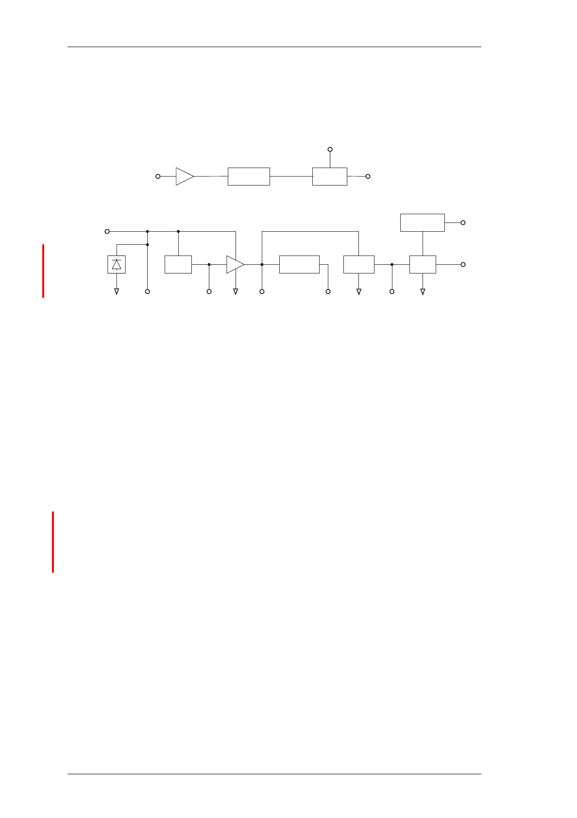
Figure 4.1 T836/837 Transmit Timers
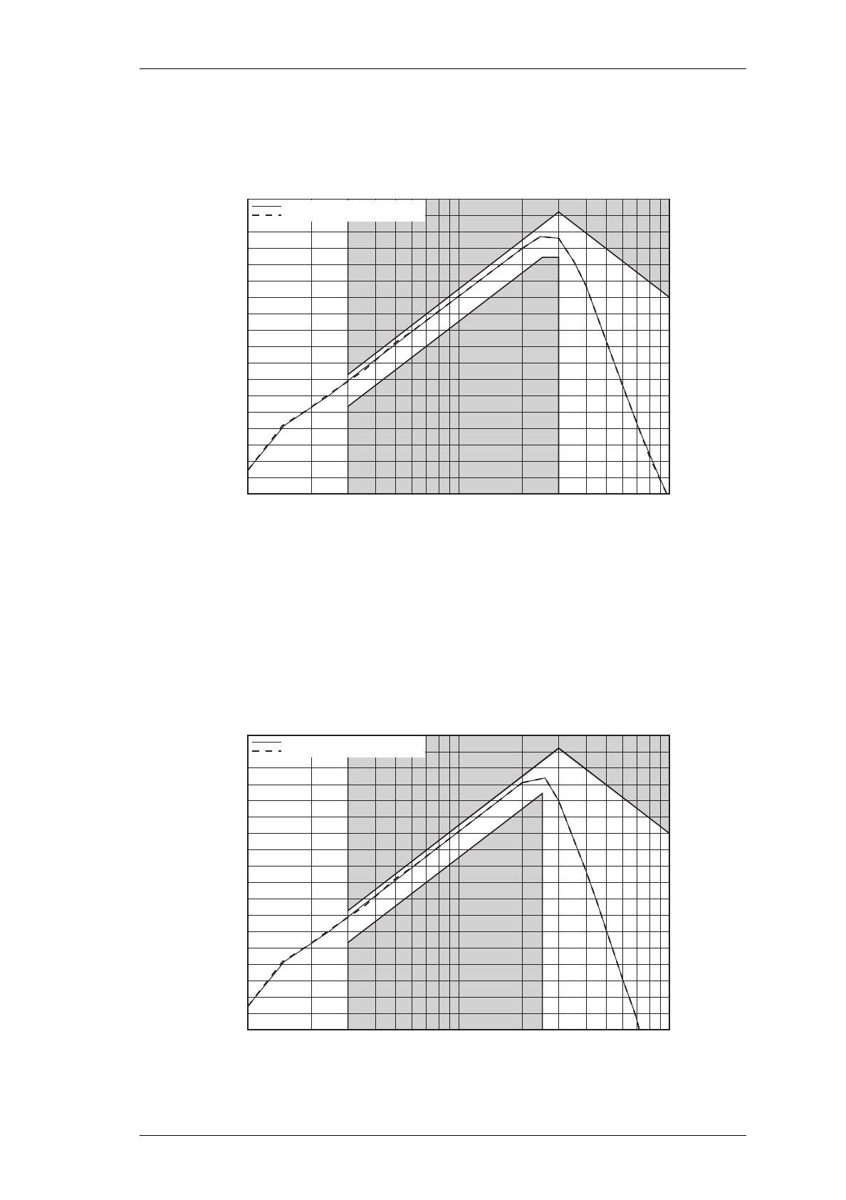
4.5 Frequency Response
If the T836/837 has been correctly adjusted, the pre-emphasis and limiting responses
should closely match those shown in Figure 4.2 and Figure 4.3 respectively.
Note:
The limits shown on these graphs should not be exceeded.
• If you are using an RF test set, turn off all filters.
• Measure the pre-emphasis response as follows:
Reduce the line level to give ±1kHz (±0.8kHz) [±0.5kHz] deviation at 1kHz.
Sweep the modulation frequency.
The response should closely match that shown in Figure 4.2.
• Measure the limiting response as follows:
Set the line level to give ±3kHz (±2.4kHz) [±1.5kHz] deviation at 1kHz.
Timer Function Adjustment
Transmit Tail Sets the tail time during which the
transmitter stays keyed after the exter-
nal key source has been removed.
0-5 seconds in 100ms
stepsa
a. Adjustable in 20ms steps in PGM800Win version 2.12 and later.
Transmit Timeout Sets the maximum continuous trans-
mission time. Once the timer has
timed out, the transmitter must be
keyed again, unless prevented by the
transmit lockout timer.
0-300 secondsb in 10
second steps
b. Adjustable from 0 to 600 seconds in PGM800Win version 2.12 and later.
Transmit Lockout Sets the period of time that must
elapse after a timeout before the trans-
mitter can re-transmit. Once the timer
has timed out, the transmitter can be
keyed again.
0-60 seconds in 10
second steps
On
Lockout Time
Timeout
Time
On
Tail Time
Tx-Enable
Tx-Reg.
Tx-Enable
Tx-Reg.
M830-00
T836/837 Functional Testing
C4.5
Copyright TEL 23/07/99
Increase the line level 20dB and sweep the modulation frequency.
The response should closely match that shown in Figure 4.3.
Figure 4.2 T836/837 Pre-emphasis Response
Wide Bandwidth
Narrow Bandwidth
Mid Bandwidth
The mid bandwidth graph is the same shape as the wide bandwidth graph. The devia-
tion figures are as follows:
peak + max. deviation = +0.8kHz
peak - max. deviation = -0.8kHz.
+10
+8
Modulation Level (dB ref. to dev. @ 1kHz)
+6
+4
+2
+0
-2
-4
-6
-8
-10
-12
-14
-16
-18
-20
-22
100 200 300 500 1k 2k 3k 5k 10k
Frequency (Hz)
Peak + max. dev. = +1.0kHz @ 1000Hz
Peak - max. dev. = -1.0kHz @ 1000Hz
+10
+8
Modulation Level (dB ref. to dev. @ 1kHz)
+6
+4
+2
+0
-2
-4
-6
-8
-10
-12
-14
-16
-18
-20
-22
100 200 300 500 1k 2k 3k 5k 10k
Frequency (Hz)
Peak + max. dev. = +0.5kHz @ 1000Hz
Peak - max. dev. = -0.5kHz @ 1000Hz
C4.6
T836/837 Functional Testing
M830-00
30/04/98 Copyright TEL
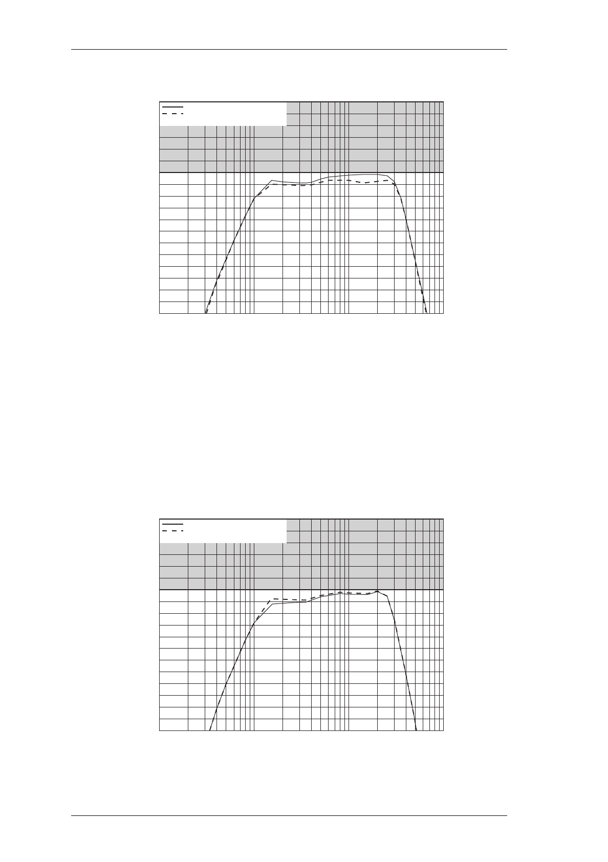
Figure 4.3 T836/837 Limiting Response
Wide Bandwidth
Narrow Bandwidth
100 500300 5k50
+10
+8
Modulation Level (dB ref. to max. dev.)
+6
+4
+2
+0
-2
-4
-6
-8
-10
-12
-14
-16
-18
-20
-22
10 20 30 200 1k 2k 3k 10k
Frequency (Hz)
Peak + max. dev. = +4.9kHz @ 1500Hz
Peak - max. dev. = -4.4kHz @ 2500Hz
Above limiting (steady-state)
Mid Bandwidth
The mid bandwidth graph is the same shape as the wide bandwidth graph. The devia-
tion figures are as follows:
peak + max. deviation = +4kHz
peak - max. deviation = -4kHz.
100 500300 5k50
+10
+8
Modulation Level (dB ref. to max. dev.)
+6
+4
+2
+0
-2
-4
-6
-8
-10
-12
-14
-16
-18
-20
-22
10 20 30 200 1k 2k 3k 10k
Frequency (Hz)
Peak + max. dev. = +2.4kHz @ 2000Hz
Peak - max. dev. = -2.5kHz @ 2000Hz
Above limiting (steady-state)

M830-00
T836/837 Functional Testing
C4.7
Copyright TEL 23/07/99
4.6 Audio Level Input Sensitivity
• Adjust RV210 (line sensitivity) fully clockwise.
• Check that the input sensitivities are better than those specified below:
Note:
A degraded signal to noise ratio can be expected with the compressor
selected. The extent of the degradation is dependent on the audio input
level.
Line Input 600 ohms, ±3kHz (±2.4kHz) [±1.5kHz] deviation at
1kHz:
with compressor -50dBm
without compressor -30dBm
Microphone Input 600 ohms, ±3kHz (±2.4kHz) [±1.5kHz] deviation at
1kHz:
with compressor -75dBm
without compressor -55dBm
CTCSS Input 1kHz deviation at 150Hz 500mV rms
Editor’s Note:
The CTCSS adjustment procedure described in Section 4.7 has been
moved to a more appropriate location in Section 3 as part of the Ini-
tial Tuning & Adjustment procedure (refer to Section 3.4.5 and Sec-
tion 3.9.3).


M830-00
T836/837 Fault Finding
C5.1
Copyright TEL 23/07/99
5 T836/837 Fault Finding
Caution:
This equipment contains CMOS devices which are susceptible to dam-
age from static charges. Refer to Section 1.2 in Part A for more infor-
mation on anti-static procedures when handling these devices.
The following test procedures and fault finding flow charts may be used to help locate a
hardware problem, however they are by no means a complete fault finding procedure.
If you still cannot trace the fault after progressing through them in a logical manner,
contact your nearest Tait Dealer or Customer Service Organisation. If necessary, you
can get additional technical help from Customer Support, Radio Systems Division, Tait
Electronics Ltd, Christchurch, New Zealand (full contact details are on page 2).
Note 1:
In this and following sections deviation settings are given first for wide
bandwidth sets, followed by settings in brackets for mid bandwidth sets ( )
and narrow bandwidth sets [ ].
Note 2:
Unless otherwise specified, the term "PGM800Win" used in this and follow-
ing sections refers to version 2.00 and later of the software.
Refer to Section 6 where the parts lists, grid reference index and diagrams will provide
detailed information on identifying and locating components and test points on the
main PCB. The parts list and diagrams for the VCO PCB are in Part E.
The following topics are covered in this section
Section Title Page
5.1 Visual Checks 5.3
5.2 Component Checks 5.3
5.3 Front Panel LED Indicator 5.3
5.4
5.4.1
5.4.2
DC Checks
Power Rails
VCO Locking
5.4
5.4
5.4
5.5
5.5.1
5.5.2
5.5.3
5.5.4
RF Checks
T836 Drive Power
T836 PA Output Power
T837 Output Power
Audio And Modulation
5.5
5.5
5.5
5.5
5.6
5.6 PGM800Win Generated Errors 5.7

C5.2
T836/837 Fault Finding
M830-00
30/04/98 Copyright TEL
5.7
5.7.1
5.7.1.1
5.7.1.2
5.7.1.3
5.7.2
5.7.3
5.7.4
5.7.5
5.7.6
5.7.7
Fault Finding Charts
Microcontroller
Basic Checks
Serial Communications
CTCSS Encode
Regulator
Synthesiser
T836 Drive Amplifier
T836 PA & Power Control
T837 Exciter Drive Amplifier
Audio Processor
5.8
5.8
5.8
5.9
5.10
5.11
5.12
5.15
5.16
5.17
5.18
5.8 To Replace The T836 PA Transistors (Q415 & Q425) 5.19
Figure Title Page
5.1
5.2
RF Diode Probe Circuit
Positioning Of Components Around Q425 & Q415
5.5
5.20
Section Title Page
M830-00
T836/837 Fault Finding
C5.3
Copyright TEL 30/04/98
5.1 Visual Checks
Remove the covers from the T836/837 and inspect the PCB for damaged or broken com-
ponents, paying particular attention to the surface mounted devices (SMD's).
Check for defective solder joints. If repair or replacement is considered necessary, refer
to Section 3 of Part A.
5.2 Component Checks
If you suspect a transistor is faulty, you can assess its performance by measuring the for-
ward and reverse resistance of the junctions. Unless the device is completely desol-
dered, first make sure that the transistor is not shunted by some circuit resistance. Use a
good quality EVM (e.g. Fluke 75) for taking the measurements (or a 20k ohm/V or bet-
ter multimeter, using only the medium or low resistance ranges).
The collector current drawn by multi-junction transistors is a further guide to their per-
formance.
If an IC is suspect, the most reliable check is to measure the DC operating voltages. Due
to the catastrophic nature of most IC failures, the pin voltages will usually be markedly
different from the recommended values in the presence of a fault. The recommended
values can be obtained from either the circuit diagram or the component data catalogue.
5.3 Front Panel LED Indicator
The green "Supply" LED on the T836/837 front panel will flash according to the condi-
tions described in the following table:
Where two or more conditions occur at the same time, the precedence is in the order
shown above (i.e. T836/837 linked has the highest priority, followed by internal error).
Flash Rate Condition
fast ( sec. on/ sec. off
approx.) T836/837 is linked with
PGM800Win
unequal ( sec. on/1 sec. off
approx.) microcontroller has detected an
internal communications error -
refer to Section 5.7.1

C5.4
T836/837 Fault Finding
M830-00
30/04/98 Copyright TEL
5.4 DC Checks
5.4.1 Power Rails
Refer to the test points and options diagrams in Section 6 for test point locations, and to
the regulator fault finding chart (Section 5.7.2) for fault diagnosis.
Check the 13.8V (TP601) and 9V (TP602) supplies at their test points in the regula-
tor compartment with a DMM.
Check the 5V (TP604) and 20V (TP603) rails at their respective test points in the
regulator compartment.
Check that Tx-Reg. (TP305 in the exciter compartment) comes up to 8.8V when the
exciter is keyed.
Check the +5V digital regulator output (TP607 in the regulator compartment).
Check for short circuits.
5.4.2 VCO Locking
Key the exciter.
Using a DMM, monitor the VCO control voltage at PL4-1 or the junction of L1 and
R1 on the VCO PCB.
If the synthesiser is locked and the VCO aligned, the voltage at this point should
be between 5 and 13V.
If the VCO is not locked, refer to the synthesiser fault finding chart (Section 5.7.3).
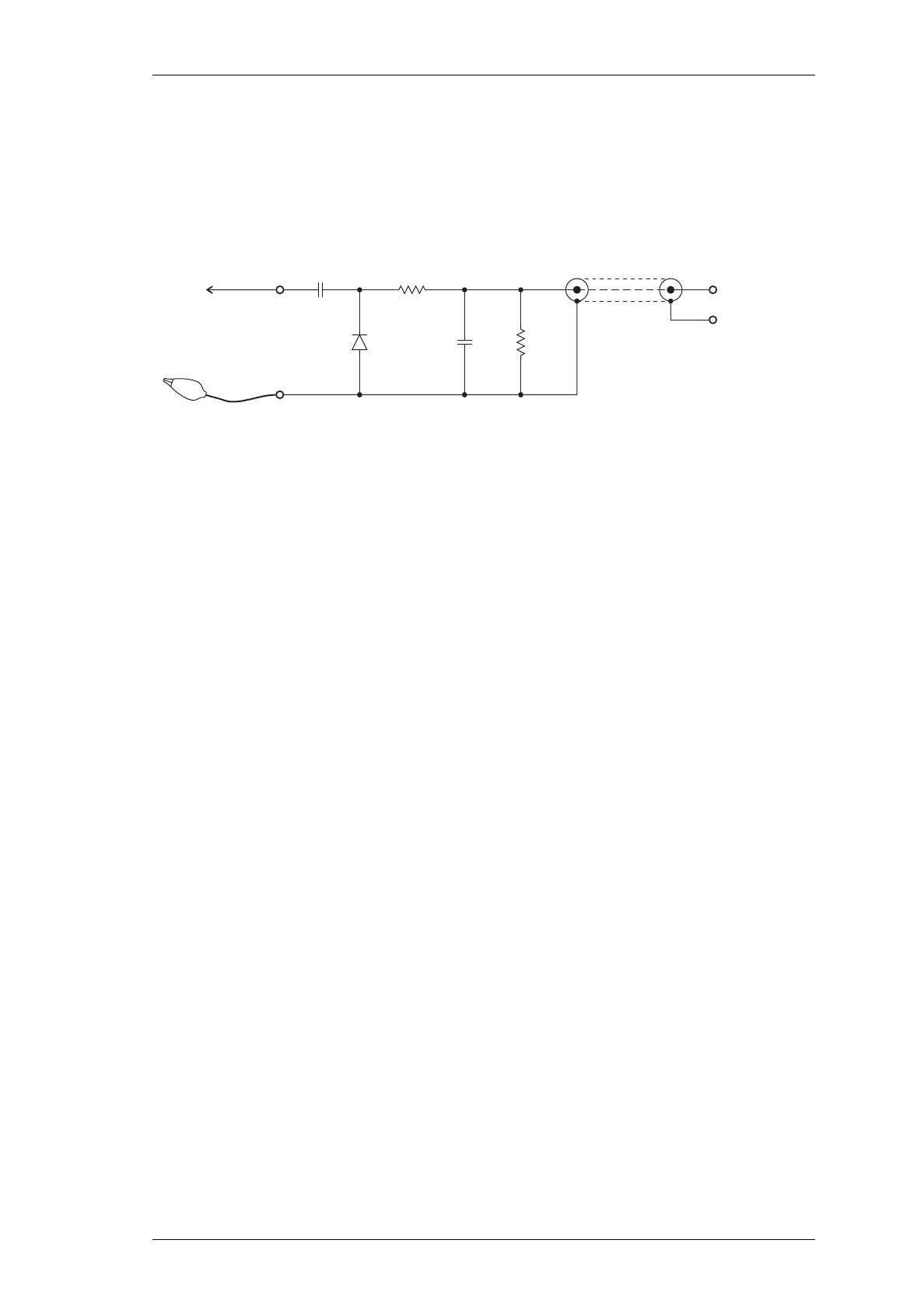
M830-00
T836/837 Fault Finding
C5.5
Copyright TEL 30/04/98
5.5 RF Checks
In-circuit RF levels may be measured with an RF probe on which the earth lead has been
shortened to a minimum (i.e. 13mm). Refer to the circuit diagrams for typical levels.
Figure 5.1 shows a suitable RF probe circuit.
Figure 5.1 RF Diode Probe Circuit
5.5.1 T836 Drive Power
Refer to the drive amplifier fault finding chart (Section 5.7.4).
Ensure that the VCO locks (refer to Section 5.4.2).
Connect the drive output to a power meter and key the transmitter.
Check that the output power is between 600 and 1000mW.
Note:
If the synthesiser is out of lock, the lock detector (synthesiser IC740 and
comparator IC750) will prevent the RF signal from reaching the PA by
switching the supply to the exciter amplifier (Q340, Q345).
5.5.2 T836 PA Output Power
Reconnect the drive output to the PA input.
Connect the PA to a power meter and key the transmitter.
Check that the output power is >30W with RV320 (power adjust) adjusted fully
clockwise.
5.5.3 T837 Output Power
Refer to the exciter drive amplifier fault finding chart (Section 5.7.6).
Ensure that the VCO locks (refer to Section 5.4.2).
100k
10k
1n
1n
1N6263
Coax
Probe
Earthing Clip
DC to DVM or
Oscilloscope
This unit is not suitable for use on high power RF circuits.

C5.6
T836/837 Fault Finding
M830-00
30/04/98 Copyright TEL
Connect the exciter output to a power meter and key the exciter.
Check that the output power is between 600 and 1000mW.
Note:
If the synthesiser is out of lock, the lock detector (synthesiser IC740 and
comparator IC750) will prevent the RF signal from reaching the PA by
switching the supply to the exciter amplifier (Q340, Q345).
5.5.4 Audio And Modulation
Refer to the audio processor fault finding chart (Section 5.7.7).
Set up the audio processor as described in Section 3.9.
Check that the demodulated RF output has the frequency response referred to in
Section 4.5 with at least ±5kHz (±4kHz) [±2.5kHz] deviation available at 1kHz
modulating frequency.
If the above result is not achieved, either the two modulators are incorrectly adjusted or
a fault condition exists.

M830-00
T836/837 Fault Finding
C5.7
Copyright TEL 30/04/98
5.6 PGM800Win Generated Errors
The following errors are those most likely to occur using PGM800Win. Refer to the
PGM800Win software user’s manual for a complete list of error messages.
Channel Switch Set
The programmed default channel change was not accepted by the base station because a
channel is selected externally. Try turning the external channel switch off to change the
default channel in PGM800Win.
Synth Out Of Lock
The synthesiser received incorrect data, or the data was corrupted. Enter a frequency
within the VCO switching range, or tune the VCO.
Internal Error
Data could not be read from the base station due to an internal error. Check for shorts
or open circuits on the SDA, SCK, SYNTH and EPOT lines. The SDA, SCK and SYNTH
are normally high, and the EPOT is normally low.
Write/Read To An Unlinked Module
The link to the module does not exist. Undefined error.
C5.8
T836/837 Fault Finding
M830-00
30/04/98 Copyright TEL
5.7 Fault Finding Charts
Note:
The standard test point designations used in this section are as follows:
TP601 13.8V
TP602 9V
TP603 20V
TP604 5V
5.7.1 Microcontroller (IC810)
5.7.1.1 Basic Checks
Pulsing Check state
of pin 35.
Y
Is pin 30
pulsing?
High or open circuit
Y
Static high/low
Check state of
pins 36 to 43.
Low/floating
High
Is the 12.8MHz clock
present on IC810 pin 21
(microcontroller)?
N
Replace
IC810.
Check IC740
(synthesiser).
*digital storage oscilloscope
Replace IC810.
Check the
state of
pin 10.
N Pulsing
Low
Replace
IC810.
Use a DSO* to check
operation of IC650
(i.e. active high
pulse at power up).
Replace
IC650.
Correct the fault causing
pin 35 to be low/floating.
M830-00
T836/837 Fault Finding
C5.9
Copyright TEL 30/04/98
5.7.1.2 Serial Communication
Check pin state.
Y
Low/floatin
g
N
Noise
on pin
Disconnect the
pro
g
rammin
g
lead.
Is IC810 pin 11 hi
g
h?
(microcontroller)
Y*di
g
ital stora
g
e
oscilloscope
Use PGM800Win
to send a POLL
command to the
radio.
Check the transistor
interface circuitry
and/or replace the
pro
g
rammin
g
lead.
Check the SERIAL-COM
and AUDIO-1/2 links.
Replace
IC810.
Check the transistor
interface circuitry
and/or replace the
pro
g
rammin
g
lead.
Check the transistor
interface circuitry.
Check IC810 pin 13
with a DSO. Is there
a response from IC810 after
a poll command is sent?
N
Y
Connect the pro
g
rammin
g
lead and use PGM800Win
to read the rack/radio.
Check I/O pad P810
with a DSO*.
Does it swin
g
from
0 to 5V?
N
C5.10
T836/837 Fault Finding
M830-00
30/04/98 Copyright TEL
5.7.1.3 CTCSS Encode
Y
Y
Y
Replace IC810.
Use PGM800Win to
select a channel
with a CTCSS tone
pro
g
rammed.
Check serial communications.
(See separate flow chart).
Cannot select a channel
Check IC810 pins 24, 25
& 26 (microcontroller).
Are there 5V square waves at
the CTCSS frequency?
Check IC830 pins 1, 7 & 14.
Are there 9V square waves at
the CTCSS frequency?
Check IC830 pin 8.
Is there a sine wave
at the CTCSS frequency? Check RV805.
No tone
Check the filter circuit for bias
problems and/or short circuits.
Distorted tone
No square waves or
uneven mark/space ratio
No square waves or
uneven mark/space ratio Check IC830 circuitry
and repair/replace.
M830-00
T836/837 Fault Finding
C5.11
Copyright TEL 23/07/99
5.7.2 Regulator
N
Y
Check for
overheatin
g
components &
short circuits.
N
Y
Check Q630,
Q620 & IC640.
N
Y
9.0V present
on TP602?
Check Q660 is
switchin
g
at
approx. 150kHz.
N
Y
20V present
on TP603?
Check R615.
Replace IC610.
N
Y
+5V present on
IC610 pin 2?
Key Tx.
YRe
g
ulators OK.
N
8.8V present
on Tx re
g
. TP305?
Replace Q610.
Y
N
0V present
on Q860 collector?
Check Q860 and
associated circuitry.
Y
0.6V present on
Q860 base?
N
Re
g
ulators OK.
Check microcontroller
section.
Check continuity
from pin 9 of
D-ran
g
e 1.
13.8V present on
IC630 pin 3?
5.3V present on
IC630 pin 1? Replace IC630.
C5.12
T836/837 Fault Finding
M830-00
23/07/99 Copyright TEL
5.7.3 Synthesiser
Refer to the synthesiser circuit diagram (sheet 7) in Section 6 and the VCO circuit dia-
gram in Part E.
N
A B
Check biasin
g
resistors, Q4 & Q5.
N
Y
N
8.3V present
at VCO?
DC V present
at Q4 & Q5?
9V present at
VCO Q4/Q5?
No VCO RF output.
Y
DC V present at
VCO, Q1, Q2 & Q3?
Check biasin
g
resistors, Q1,
Q2 & Q3.
Y
N
Capacitors OK?
Check for cracks,
shorts, etc.
N
Y
Replace VCO.
Replace
if faulty.
Y
N
Y
N
N
N
Y
Y
DC V present
on Q795 emitter?
Check 9V supply.
9V present on
Q795 divider buffer?
20V inverter
supply faulty.
20V present
on IC750 pin 8?
Check 5V re
g
. &
supply resistor
to each IC.
+5V present at
IC700, IC710,
IC740, IC720
& IC730?
VCO out of lock.
Y
Y
Y
Continued on the next pa
g
e
Y
Does VCO trimmer
adjust for stable
control line
between 5 & 13V?
VCO freq. correct?
Does VCO trimmer
adjust for required
frequency ran
g
e
between 5 & 13V?
Synthesiser OK.
VCO trimmer
freq. ran
g
e OK?
Check VCO tunin
g
caps & trimmer.
Is 8MHz VCO ran
g
e
achieved between
5 & 13V?
VCO OK.
N
N
NN
N
Y
Y
Recheck
pro
g
rammin
g
via PGM800Win.
Check Q5 C
multiplier
(synth).
Check biasin
g
resistors & Q795.
Check #C5, #C3, #C4,
CV1 & D1-D4 in VCO.
Check Tx re
g
.,
Q610 & 9V re
g
.
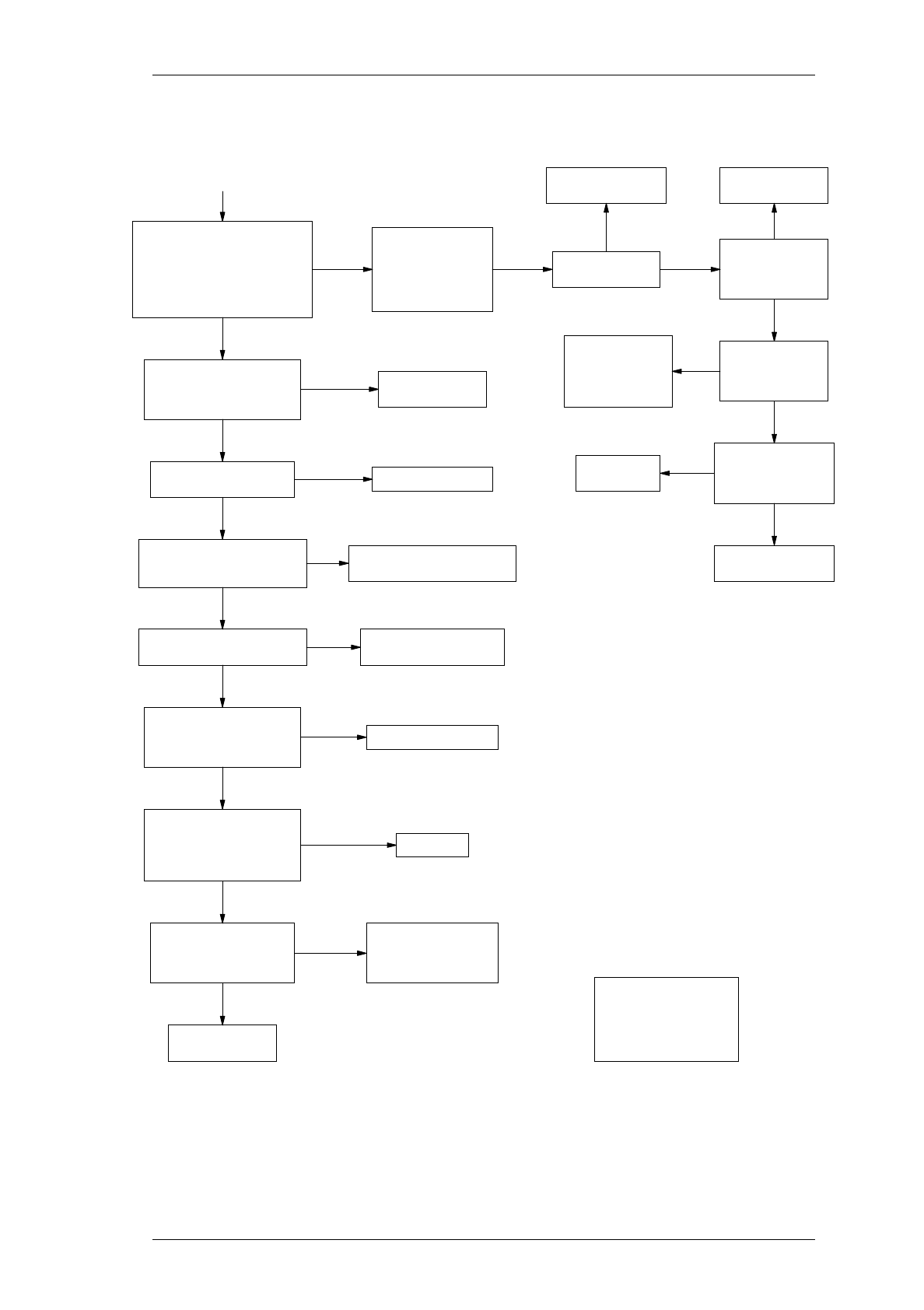
M830-00
T836/837 Fault Finding
C5.13
Copyright TEL 30/04/98
Programming and
serial bus OK?
Check programming.
Check serial bus
when programming
i.e. clock/data/enable
activity (IC740 pins
18, 19 & 17). N
Check loop filter components
R775, C774, C776, R510,
C505, IC750. Is the supply
to IC750 +20V +4, -2V?
Check regulator circuitry.
Check C772, R774, R772,
C770, R763 & Q790.
Check Q760, Q780,
R766 & C765.
Check charge pump components
(Q775 & Q780) and Q790.
Check R762 & C762.
Check the signal path from
the VCO to synthesiser.
Measure the frequency from
the VCO at IC740 pin 11 using
a frequency counter.
Is the level >-10dBm?
Does the frequency adjust
as the VCO trimmer is
adjusted (out of lock)?
Check VCO.
Y
Y
Y
Signal
Y
Y
Y
No signal
Replace synthesiser
(IC740).
Y
N Y
Y
N
N
N
N
Check phase detector output
pins (IC740 pins 3 & 4).
Are there very narrow pulses
(~50ns) at the reference frequency?
(i.e. 5kHz : 200µs period
6.25kHz : 160µs period)
*See Note below.
Is the charge pump bias
voltage at the base of
Q760 & Q780 between
3.5 and 5V? (5V when locked)
N
Is the voltage on C762,
R760, and R758 9V ±0.2V?
Is the loop filter reference
voltage at C772 (+) 6.5V ±0.2V?
N
Check divider buffer
circuit (Q795) and bias
voltages on Q795 emitter
(1.3V ±0.2V).
*Note:
When locked, both of these
are very narrow (~50ns).
If unlocked, one will be
very narrow (~50ns),
and the other wide (>15µs).
Replace synthesiser
(IC740).
Continued from previous page
B
Is the charge pump voltage
on Q790 gate between
3 and 8.5V? (6.5V ±0.2V locked)
Is reference
clock present
at IC740 pin 20
(200kHz >4.5Vpp)?
Check microcontroller
section (IC810).
N
Is reference
clock present
at IC730 pin 12
(200kHz >4.5Vpp)?
Is reference
clock present
at IC730 pin 1
(12.8MHz >4.0Vpp)?
Check TCXO (IC700)
and buffers (IC710).
N
N
Y
Y
Check phase
modulator sections:
IC720, Q710, Q720,
D710, Q730, Q740,
D720.
Check divider
IC730.
C5.14
T836/837 Fault Finding
M830-00
30/04/98 Copyright TEL
Y
N
Y
Y
VCO phase locked?
5-13V present on
control line?
Correct DC V
present on Q1 VCO?
N
Check inductors,
biasing resistors
& Q1.
Replace if faulty.
Go to B.
Loop filter &
components around
op. amp. (IC750) OK?
N
Noisy synth;
poor residual FM.
C
Isolate audio
modulation on VCO;
still noisy? Trace audio fault.
Y
Y
N
Y
Y
Y
Change trimmer;
still noisy?
Change Q1;
still noisy?
Change TCXO;
still noisy?
Change varactors;
still noisy?
Replace VCO
assembly.
Synthesiser OK.
N
N
N
N
Y
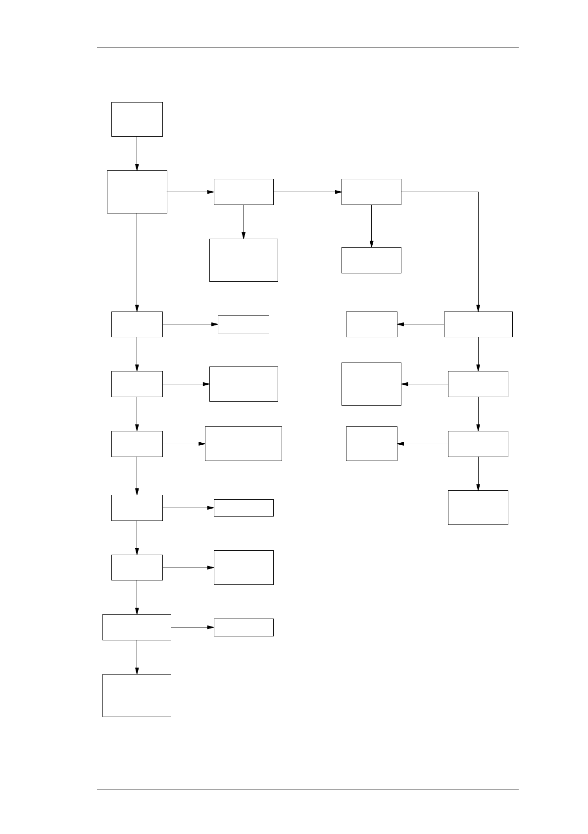
M830-00
T836/837 Fault Finding
C5.15
Copyright TEL 30/04/98
5.7.4 T836 Drive Amplifier
3.5V on Q365
collector?
10.5V on Q370
collector?
10.5V on Q315
collector?
Check continuity
of power rails
& DC paths to
Q365 & Q370.
>2.2V RF at
R359/R360?
>1.1V RF at
R360/R362?
Check attenuator
pad R359, R360,
R362.
>0.5V RF at
Q365 base?
Check C362, C365,
C368, Q365, D340,
D350, D360, L311.
>6V RF at
C379, L360? Check Q365.
>1.5V RF at
Q370 base.
Check signal
path between
Q365 & Q370.
>6V RF at
Q370 collector? Check Q370.
Check signal
path to output
incl. output
socket (SK310).
11V on IC330
pin 8?
Check Q310,
Q315 circuitry
& IC330.
Key exciter
& lock
synthesiser.
11V on IC330
pin 1?
NN N
YY
Y
Check VCO.
N
Y
N
Y
N
Y
N
Y
N
Y
N
Y
Check 9V &
13.8V supplies.
Check
regulators.
Check TP308
>+8V.
Check temp.
shutdown
circuit.
N
Y
N
Y
N
Y
Check lock det.
path back to
synth. IC740,
IC750, Q345.
Check TP314
<0.6V.
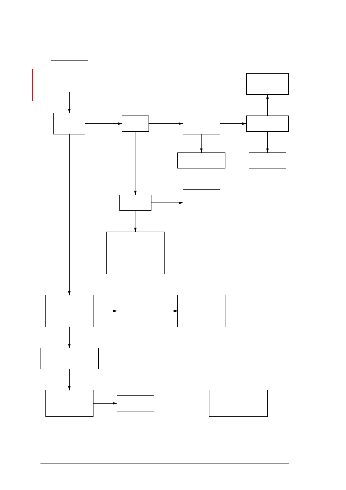
C5.16
T836/837 Fault Finding
M830-00
23/07/99 Copyright TEL
5.7.5 T836 PA & Power Control
10.5V
at L375?
Check Q415,
Q425 & circuitry,
LP filter.
Check +13.8V at
Q425 & Q415.
Check IC330,
Q310, Q315
& circuitry,
+13.8V supply.
Refer to Drive Amp.
Fault Findin
g
Chart. Check supply
circuitry.
Tx deliverin
g
full power
(>30W)?
Set RV320
(power adjust)
fully clockwise;
synth. locked;
key Tx.
<2.7V on
IC330 pin 2?
Check lock det. circuit;
TP308 should be >8V.
Check temp. shutdown
circuit (IC330);
TP314 should be <0.6V.
Check Q305, RV330.
Turn RV320 ccw.
Check power
drops to zero
slowly in a
controlled manner.
Does variation
of RV320
cause either
full power
or no power?
Check for break
in power sense
circuitry; directional
coupler D410,
D420 & circuitry.
Y
NY
NN
Y
N
Y
N
NY
Y
Check drive
at SK310
600-1000mW.
Y
Set RV320 so that
output power = 25W;
check L375 approx. 7V.
Momentarily remove
Tx load. Volta
g
e at
L375 decreases to
approx. 6.5V?
Power control
circuitry OK.
Note:
c/w = clockwise
cc/w = counterclockwise
or anticlockwise
Y
Normal operating conditions:
Forward power ≅1.6V
Reverse power ≅0.25V
IC330 pin 2 ≅2.7V
IC330 pin 3 ≅2.7V
IC330 pin 1 ≅9V
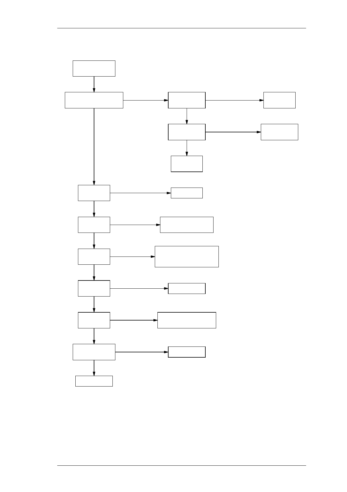
M830-00
T836/837 Fault Finding
C5.17
Copyright TEL 30/04/98
5.7.6 T837 Exciter Drive Amplifier
10.5V at Q315
collector?
Check IC330,
R324 & R326.
Check Q310
& Q315.
>2.2V RF at
R359/R360?
>1.1V RF at
R360/R362?
>0.5V RF at
Q365 base?
>6V RF at
C379, L360?
>1.5V RF at
Q370 base?
Check attenuator pad
R359, R360, R362.
Check Q365.
Check si
g
nal path
between Q365 & Q370.
Check Q370.
3.5V at Q365 collector?
10.5V at Q370 collector? Check
power rails.
>5V present on
IC330 pin 1?
Key exciter &
lock synthesiser.
Check VCO.
Check C362, C365, C368,
Q365, L311, D340, D350,
& D360.
>6V RF at
Q370 collector?
Drive amp. OK.
NY
YN
N
Y
N
Y
N
Y
N
Y
N
Y
N
Y
N
Y
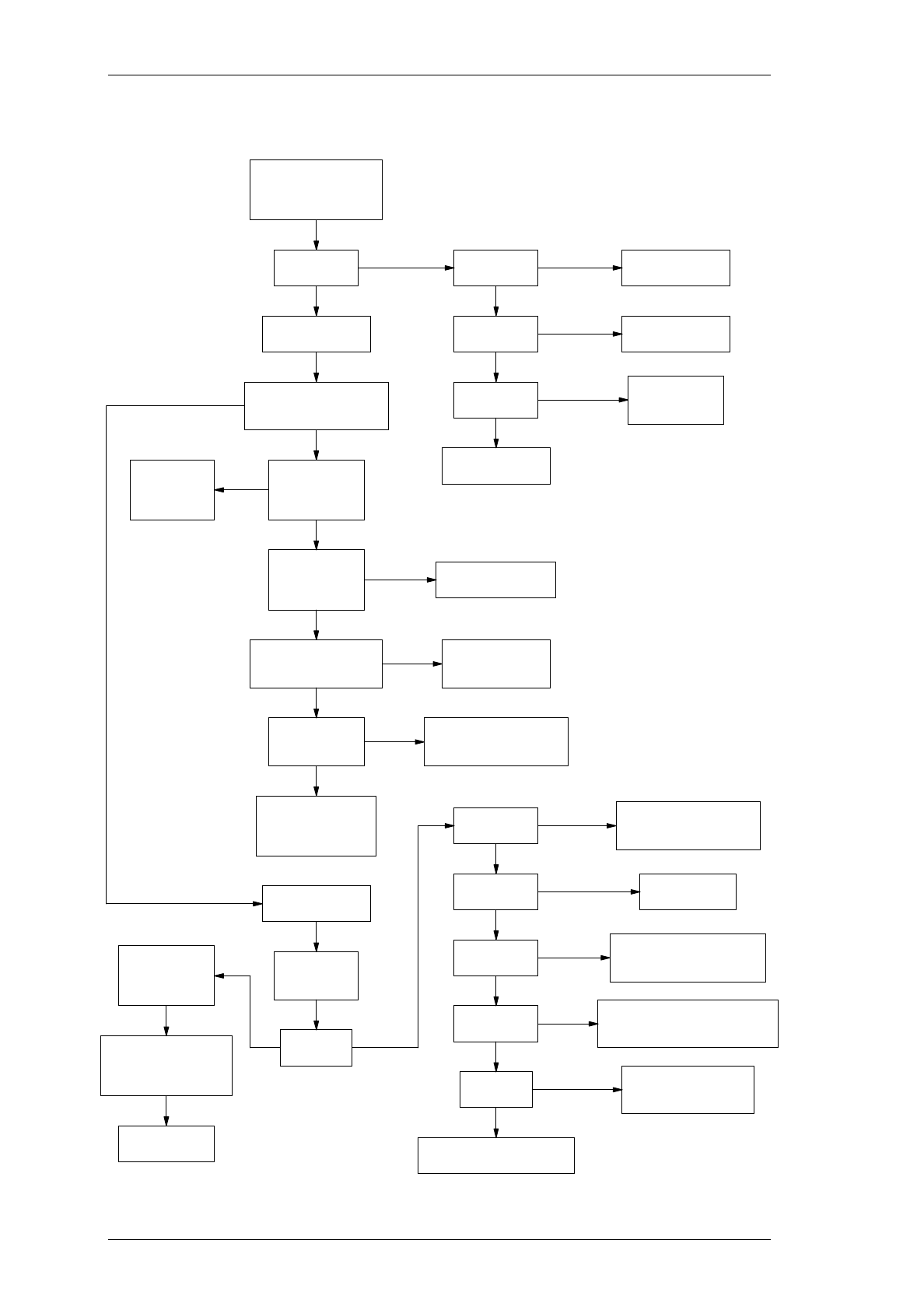
C5.18
T836/837 Fault Finding
M830-00
30/04/98 Copyright TEL
5.7.7 Audio Processor
N
IC240 pin 6
at 9V?
Key exciter &
lock synthesiser.
Connect 1kHz audio
to external CTCSS input.
Does exciter
modulate? Audio output at
IC260 pin 8?
NY
Check audio path to
VCO control line.
Check alignment
of modulators.
YN
Audio output at
IC260 pin 1?
YCheck buffer IC260
pins 8, 9 & 10.
N
Audio output at
IC260 pin 7?
Check low pass
filter stage IC260
pins 1, 2 & 3.
Y
Check stage IC260
pins 5, 6 & 7.
N
Demodulated audio
frequency response
flat between 50 & 300Hz?
Y
Check low
pass filter
stage IC260
pins 1, 2 & 3.
N
N
Y
Audio frequency
response IC260
pin 1 flat 300Hz
to 2kHz?
Audio frequency
response IC210
pin 8 6dB/octave
slope?
Check integrator
IC210 pins 8, 9, & 10.
N
Y
Audio superimposed
on 200kHz signal
IC720 pins 9 & 3 (synth)?
Check audio path
between integrator
& phase modulator.
N
Y
200kHz clipped
triangle wave at
IC720 pins 8 & 4?
Check IC720, Q710, Q720,
Q730, Q740, D710, D720,
C727, C729, C724 & C725
N
Y
Check loop filter
(IC750, pins 5, 6 & 7)
& associated
components.
Select standard
audio configuration.
Check pre-emphasis
network IC230 pins 12,
13 & 14 &/or low pass
filter IC260 pins 1, 2 & 3.
N
Y
Connect audio
to line input;
key exciter.
Does exciter
modulate?
YN
Demodulated
audio frequency
response as per
Section 4.5?
Audio processor
OK.
Audio signal at
IC210 pin 14?
Y
N
Audio signal at
IC230 pin 1?
N
Audio signal at
IC230 pin 14?
Y
N
Audio signal at
IC240 pin 4?
Y
N
Y
Check Q260 is not faulty or
being turned on inadvertently.
Y
Check audio path between
limiter IC210 pin 14 &
summing amp. IC260 pin 7.
Check IC210
pins 12, 13 & 14.
Check IC230 pins 1, 2 & 3 or
audio path between pre-
emphasis network & limiter.
Check IC230 pins 12, 13 & 14
or audio path between multiplexer
& pre-emphasis network.
Check IC240 or audio
path between line trans-
former & multiplexer.

M830-00
T836/837 Fault Finding
C5.19
Copyright TEL 23/07/99
5.8 To Replace The T836 PA Transistors
(Q415 & Q425)
Caution:
Failure to comply with the following procedure can result in failure of
the device due to poor heatsinking, or worse, can endanger the health
of the assembler if the beryllium oxide die carrier is smashed during
assembly.
Caution:
As the location of certain components in the PA is critical to perform-
ance, it is important that any components removed or disturbed are
refitted in exactly the same position.
Caution:
Before attempting to remove a transistor, note the position, type and
value of each capacitor and resistor so that it can be replaced in exactly
the same position (refer to Figure 5.2).
Caution:
Do not apply too much heat or pressure to the PCB pads and tracks as
you may damage them or lift them from the PCB, causing permanent
damage to the transmitter.
Remove the resistors and/or chip capacitors from around the transistor.
Desolder the transistor tabs by heating with a soldering iron and lifting away
from the PCB with a screwdriver or thin stainless steel spike. Unscrew the transis-
tor stud nut and remove the device.
Remove any excess solder from the PCB pads with solder wick.
Trim the tabs of the replacement transistor so that the device sits neatly on the
PCB pads provided.
Lightly tin the underside of the transistor tabs. Remove any excess solder to leave
a thin, even layer on the tabs.
Apply a small amount of heatsink compound (Dow-Corning 340 or equivalent) to
the transistor mounting surface. Sufficient compound should be used to ensure
an even film over the entire mounting surface.
Place the transistor on the PCB in the correct orientation and ensure the tabs are
flush to the surface. Lightly solder one tab to the PCB. Torque down the retaining
nut to the correct torque (0.7Nm/6in.lbf.).
Caution:
Do not solder all the tabs before torquing down otherwise the device
may be broken.
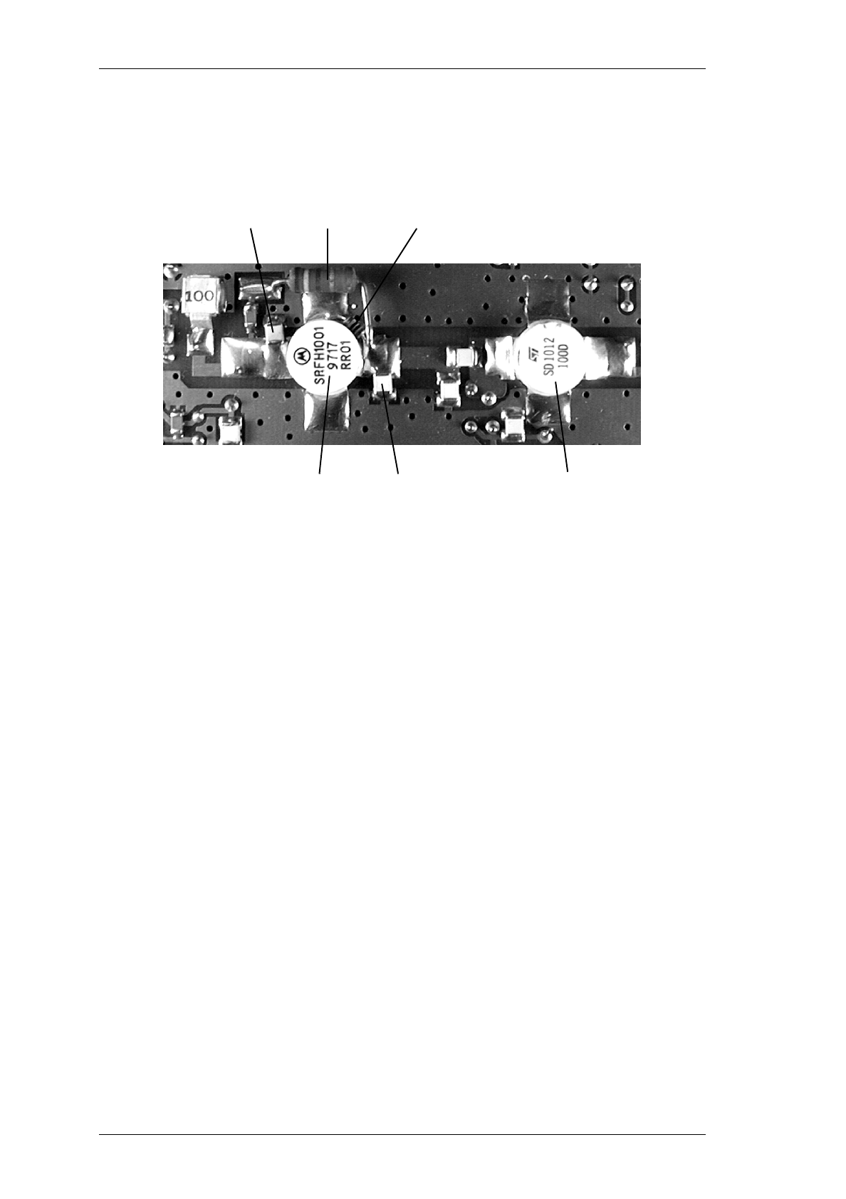
M830-00
T836/837 PCB Information
C6.1.1
Copyright TEL 23/07/99
6 T836/837 PCB Information
Caution:
This equipment contains CMOS devices which are susceptible to damage from
static charges. Refer to Section 1.2 in Part A for more information on anti-static
procedures when handling these devices.
This section provides the following information on the T836 transmitter and T837 exciter:
•parts lists
• grid reference indexes
• mechanical assembly drawings
•PCB layouts
• test points & options connections drawings
• circuit diagrams.
Section Title IPN Page
6.1 Introduction 6.1.3
6.2 T836 Transmitter PCB 220-01395-02 6.2.1
6.3 T837 Exciter PCB 220-01390-02
220-01390-03
6.3.1
6.3.27

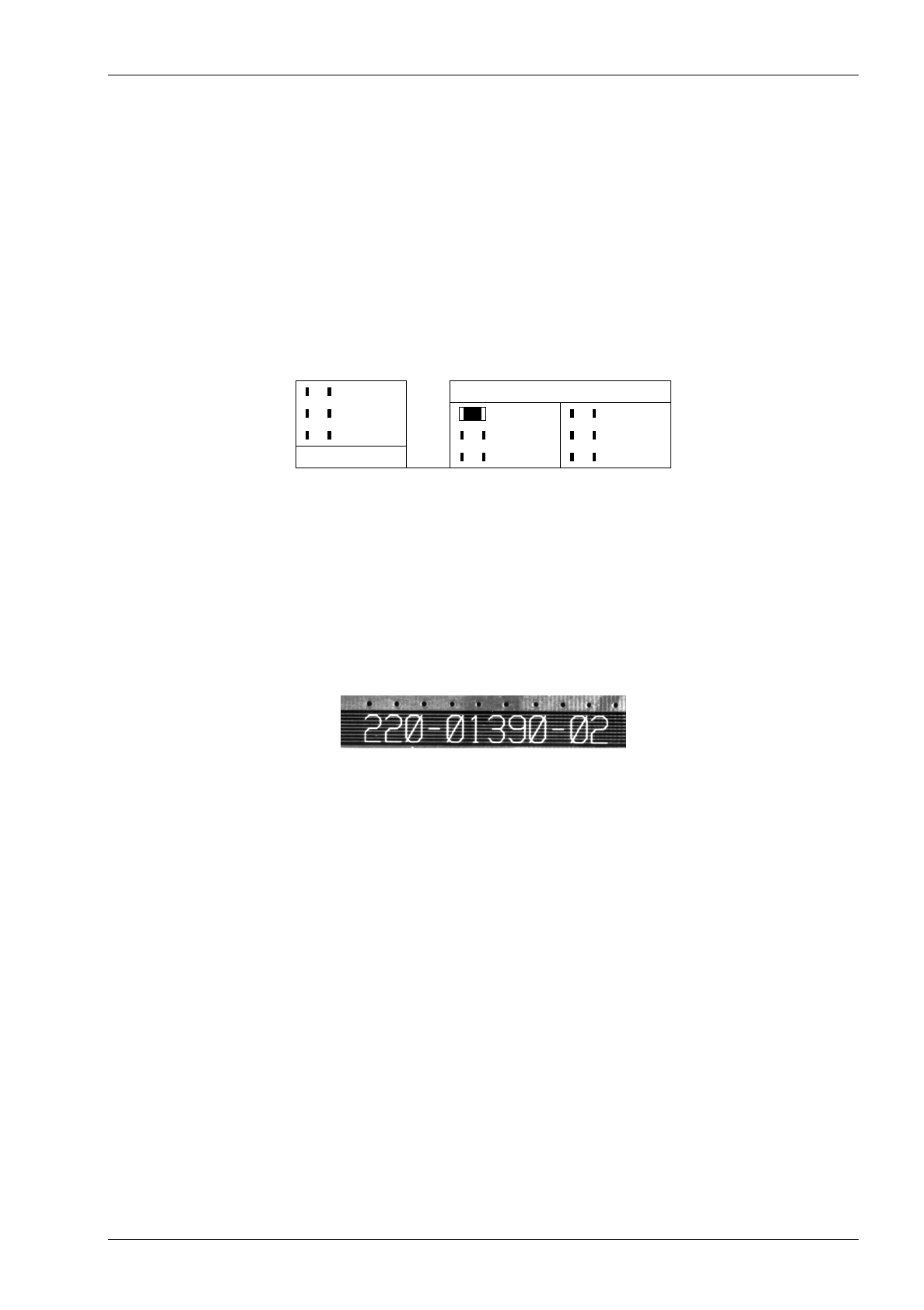
M830-00
T836/837 PCB Information
C6.1.3
Copyright TEL 30/04/98
6.1 Introduction
Product Type Identification
You can identify the transmitter or exciter type by checking the product code printed on a label on
the rear of the chassis (product codes are explained in Section 1.3 in this Part of the manual, and Fig-
ure 1.1 in Part A shows typical labels). You can further verify the product type by checking the
placement of an SMD resistor in the table that is screen printed onto the top side of the PCB, similar
to the example drawn below (this table also appears in the resist layer on the bottom side of the
PCB). In this example, the resistor indicates that the product was built as a T836-10-XXXX.
Note:
The only function of this resistor is to indicate the product type. It has no effect on the
circuitry or operation of the transmitter or exciter.
PCB Identification
All PCBs are identified by a unique 10 digit “internal part number” (IPN), e.g. 220-12345-00, which
is screen printed onto the PCB (usually on the top side), as shown in the example below:
The last 2 digits of this number define the issue status, which starts at 00 and increments through 01,
02, 03, etc. as the PCB is updated. Some issue PCBs never reach full production status and are there-
fore not included in this manual. A letter following the 10 digit IPN has no relevance in identifying
the PCB for service purposes.
Note:
It is important that you identify which issue PCB you are working on so that you can
refer to the appropriate set of PCB information.
836- PRODUCT TYPE
836- 836-10 836-20
836- 836-13 836-23
PRODUCT TYPE 836-15 836-25
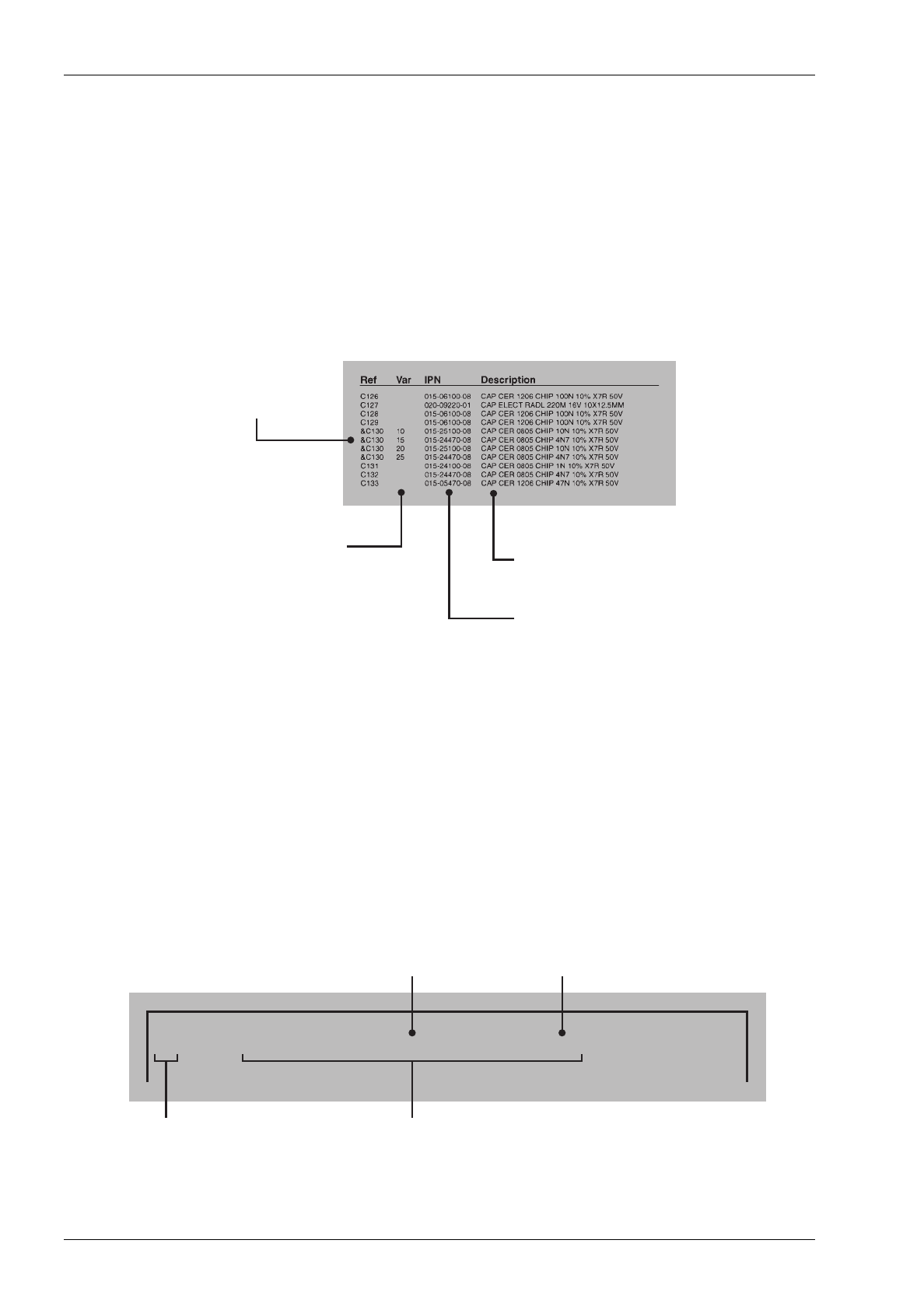
C6.1.4
T836/837 PCB Information
M830-00
30/04/98 Copyright TEL
Parts Lists
The 10 digit numbers (000-00000-00) in this Parts List are “internal part numbers” (IPNs). We can
process your spare parts orders more efficiently and accurately if you quote the IPN and provide a
brief description of the part.
The components listed in this parts list are divided into two main types: those with a circuit refer-
ence (e.g. C2, D1, R121, etc.) and those without (miscellaneous and mechanical).
Those with a circuit reference are grouped in alphabetical order and then in numerical order within
each group. Each component entry comprises three or four columns, as shown below:
The mechanical and miscellaneous section lists the variant and common parts in IPN order.
Parts List Amendments
At the front of the parts list is the Parts List Amendments box (an example of which is shown
below). This box contains a list of component changes which took place after the parts list and dia-
grams in this section were compiled. These changes (e.g. value changes, added/deleted compo-
nents, etc.) are listed by circuit reference in alphanumeric order and supersede the information
given in the parts list or diagrams. Components without circuit references are listed in IPN order.
The number in brackets at the end of each entry refers to the Tait internal Change Order document.
circuit reference -
lists components
in alphanumeric
order
variant column -
indicates that this is
a variant component
which is fitted only to
the product type listed
Internal Part Number -
order the component
b
y
this number
description -
gives a brief description
of the component
Parts List Amendments
R306 Changed from 180Ωto 560Ω(036-13560-00) to increase sensitivity (71003).
circuit reference
or IPN description
of change
IPN of new
component Change Order
number
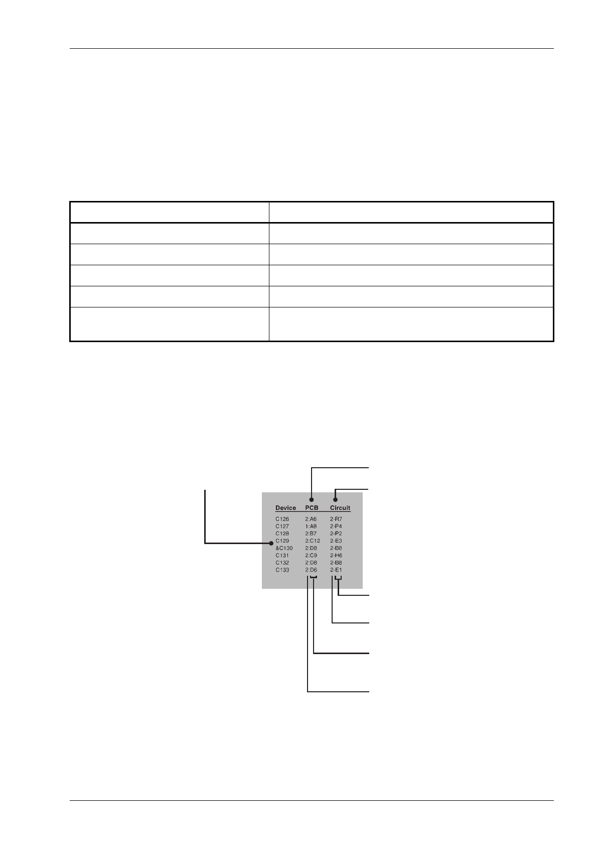
M830-00
T836/837 PCB Information
C6.1.5
Copyright TEL 30/04/98
Variant Components
A variant component is one that has the same circuit reference but different value or specification in
different product types. Where two products share the same PCB, the term “variant” is also used to
describe components unplaced in one product. Variant components have a character prefix, such as
“&”, “=” or “#”, before the circuit reference (e.g. &R100).
The table below explains the variant prefixes used in T800 Series II products:
Grid Reference Index
This section contains a component grid reference index to help you find components and labelled
pads on the PCB layouts and circuit diagrams. This index lists the components and pads in alpha-
numeric order, along with the appropriate alphanumeric grid references, as shown below:
If the variant prefix is. . . the component will. . .
& change according to channel spacing
= change according to frequency stability
# change according to frequency range
% be placed or unplaced for special applications
*be unplaced in one product
(where two products share the same PCB)
circuit diagram
reference
PCB layout
reference
components listed
in alphanumeric order
layer number -
1 = top side layer
2 = bottom side layer
component location
on the layer
sheet number
component location
on the sheet
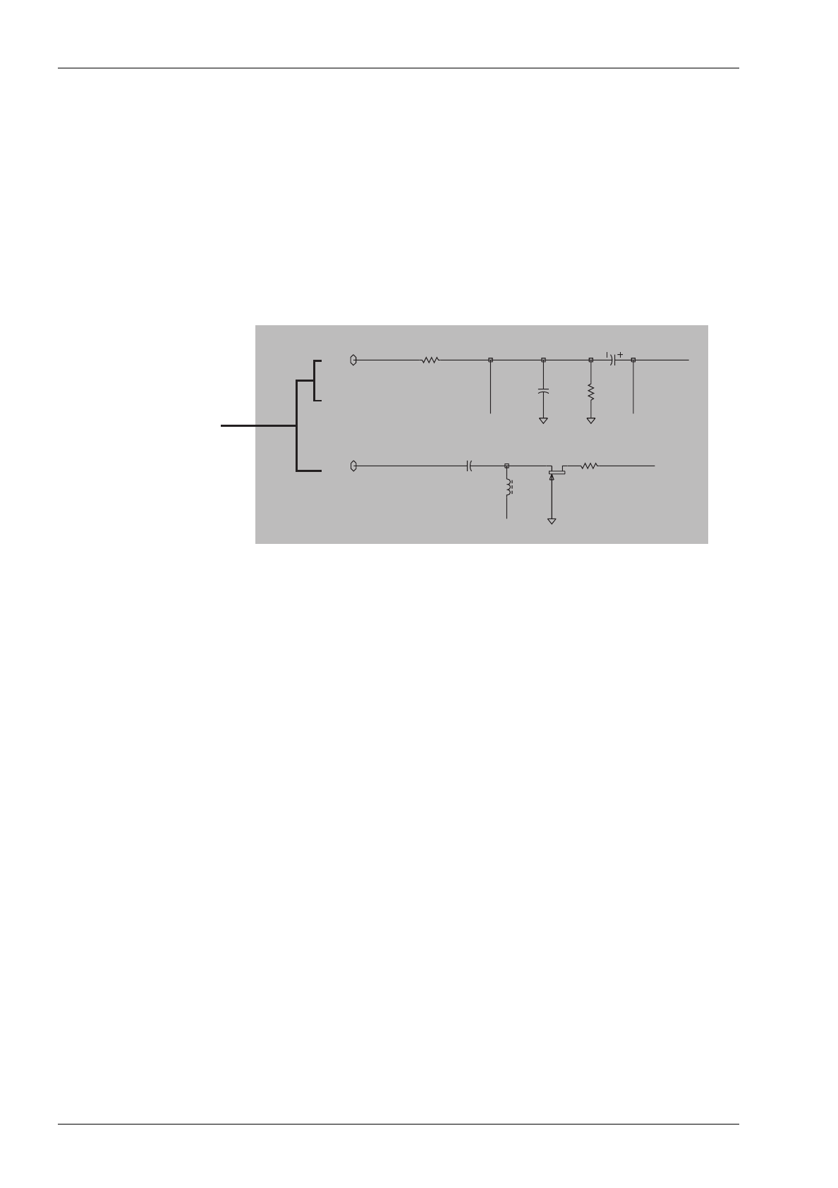
C6.1.6
T836/837 PCB Information
M830-00
30/04/98 Copyright TEL
Using CAD Circuit Diagrams
Reading a CAD circuit diagram is similar to reading a road map, in that both have an alphanumeric
border. The circuit diagrams in this manual use letters to represent the horizontal axis, and num-
bers for the vertical axis. These circuit diagram “grid references” are useful in following a circuit
that is spread over two or more sheets.
When a line representing part of the circuitry is discontinued, a reference will be given at the end of
the line to indicate where the rest of the circuitry is located, as shown below. The first digit refers to
the sheet number and the last two characters refer to the location on that sheet of the continuation of
the circuit (e.g. 1R3).
C301
4N7
R303
12
D
S
G
L310
33U
IF-SIG
4R4
C369
100P
C371
10U
R339
100K
%R338
100
DISCRIMINATOR
1R3
2R9
2R9
8A2
t
hese grid references
s
how where the circuit
is continued