Tait TEL0047 One way paging transmitters T836-26-1010 & T836-26 User Manual 8c300 a3 bk
Tait Limited One way paging transmitters T836-26-1010 & T836-26 8c300 a3 bk
Tait >
Contents
- 1. T836 Diagram of units
- 2. Installation Guide
- 3. Manual
T836 Diagram of units

M830-00
T836/837 General Information
C1.3
Copyright TEL 30/04/98
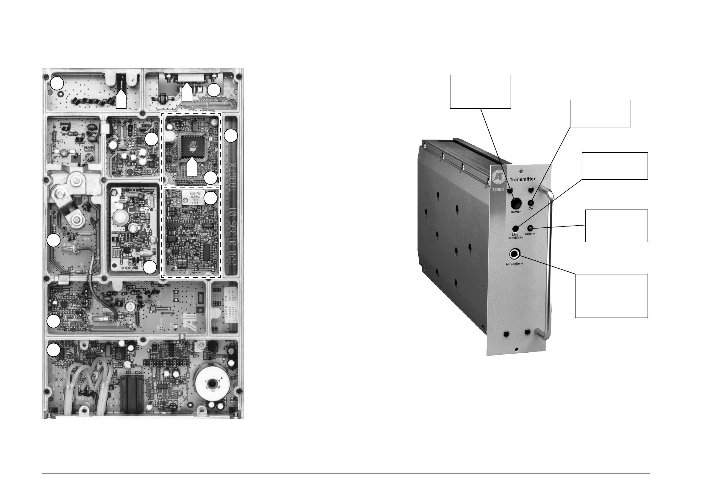
The photograph in Figure 1.1 on the next
page will help you to identify the main
circuit blocks in the T836.
There is a similar photograph in Figure
4.4 which shows the main tuning and
adjustment controls.
Extending both these fold-outs will
allow you to refer to both photographs
while using the manual.
The photograph in Figure 1.2 on the next
page shows the T836 front panel con-
trols.
C1.4
T836/837 General Information
M830-00
30/04/98 Copyright TEL
Figure 1.1 T836 Main Circuit Block Identification Figure 1.2 T836 Front Panel Controls
1
234
56
7 8
A
B
C
9
10
Key:
1
2
3
4
5
6
7
low pass filter
PA
exciter drive amplifier
audio processor
VCO
regulators
synthesiser
8
9
10
A
B
C
microcontroller and CTCSS
duct for cabling to extra D-range (if fitted)
D-range
RF output
D-range connector (“D-range 1”) incl. audio in & DC in
(refer to Section 2.2 in Part F)
microcontroller
On LED
The On LED is lit when the
T836 is transmitting.
Carrier Switch
Keys the transmitter (while
disabling the 600Ω line and
microphone audio).
Supply LED
The Supply LED is lit when
DC power is supplied to the
transmitter.
Line Sensitivity
Sets the gain of the 600Ω line
input of the audio processor.
Microphone Socket
For connecting a T800-80 micro-
phone to allow local control of
the transmitter. The 600Ω line is
disabled when the PTT button is
pressed.

M830-00
T836/837 General Information
C1.5
Copyright TEL 30/04/98
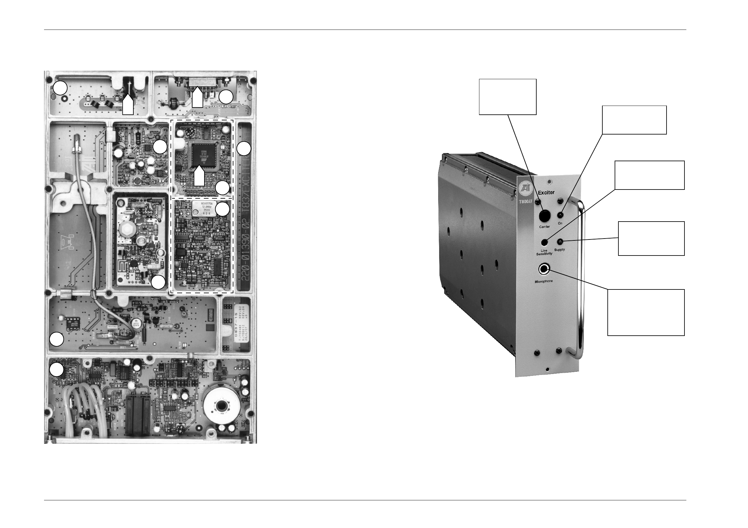
The photograph in Figure 1.3 on the next
page will help you to identify the main
circuit blocks in the T837.
There is a similar photograph in Figure
4.5 which shows the main tuning and
adjustment controls.
Extending both these fold-outs will
allow you to refer to both photographs
while using the manual.
The photograph in Figure 1.4 on the next
page shows the T837 front panel con-
trols.
C1.6
T836/837 General Information
M830-00
30/04/98 Copyright TEL
Figure 1.3 T837 Main Circuit Block Identification Figure 1.4 T837 Front Panel Controls
1
23
45
6
8
9
A
B
C
7
Key:
1
2
3
4
5
6
7
low pass filter
exciter drive amplifier
audio processor
VCO
regulators
synthesiser
microcontroller and CTCSS
8
9
A
B
C
duct for cabling to extra D-range (if fitted)
D-range
RF output
D-range connector (“D-range 1”) incl. audio in & DC in
(refer to Section 2.2 in Part F)
microcontroller
On LED
The On LED is lit when the
T837 is transmitting.
Carrier Switch
Keys the exciter (while
disabling the 600Ω line
and microphone audio).
Supply LED
The Supply LED is lit when
DC power is supplied to the
exciter.
Line Sensitivity
Sets the gain of the 600Ω line
input of the audio processor.
Microphone Socket
For connecting a T800-80 micro-
phone to allow local control of
the exciter. The 600Ω line is dis-
abled when the PTT button is
pressed.
M830-00
T836/837 Functional Testing
C4.9
Copyright TEL 30/04/98
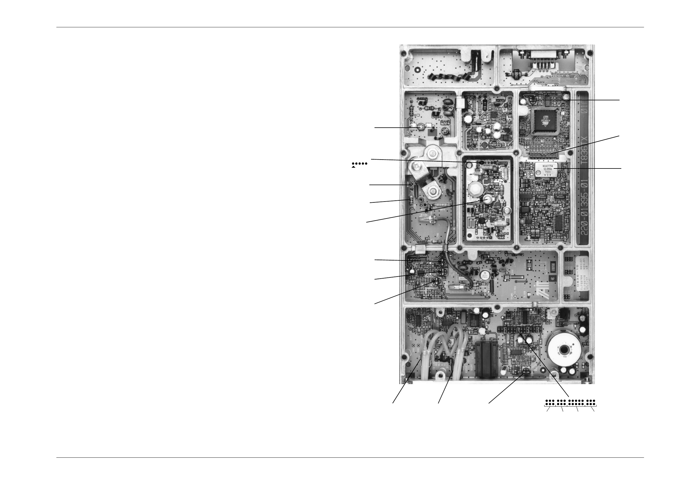
Figure 4.4 T836 Main Tuning & Adjustment Controls
R460
CV451
CV1
PL4-1
RV330
high temperature
RV320
power adjust
RV210
line sensitivity
SW230
carrier
IC700
TCXO
L490
power adjust
RV310
temperature adjust
RV220
compression level
RV805
CTCSS
level adjust
PL205 PL220 PL215 PL210
SK805
The photograph printed at right
will help you to identify the main
controls used in tuning and adjust-
ing the T836.
There is a similar photograph in
Figure 1.1 which shows the main
circuit blocks.
Extending both these fold-outs will
allow you to refer to both photo-
graphs while using the manual.