Tait TEL0061 Paging Transmitter User Manual PagingBoardFitInstruction
Tait Limited Paging Transmitter PagingBoardFitInstruction
Tait >
Contents
PagingBoardFitInstruction
8T800-32-0010 Fitting Instructions 419-83210-00 419-83210-00 T800-32-0010 Fitting Instructions 1
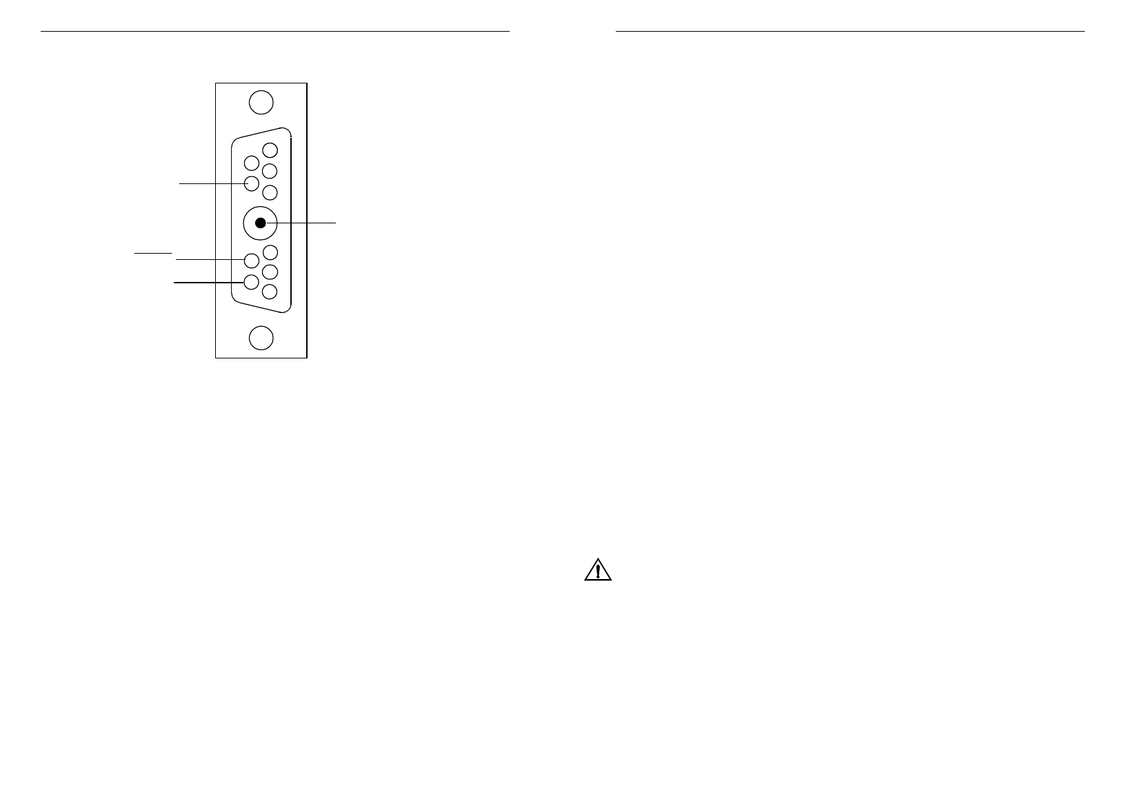
Figure 8 Pinouts for D-Range 2
1
2
3
4
5
6
8
9
10
2004f_01
DATA
DATA
Lock detect
Coaxial socket
(external
reference
frequency)
7
T800-32-0010 Paging Board
The T800-32-0010 PCB can be fitted to Tait T800 Series II transmitters to ena-
ble them to function as low-speed paging transmitters. This paging board is
for transmitters that will be connected to an external frequency standard. It is
a DFSK Modulator, suitable for POCSAG or similar paging data formats. Ref-
erence frequency stability is determined by the stability of the external stand-
ard. The PCB is not designed for use with 66 to 88MHz equipment.
Newer T800 transmittters have a Micromatch connector in the audio proces-
sor compartment. This simplifies installation.
This fitting instruction describes how to fit the PCB into existing T800 trans-
mitters. You need to be proficient in the soldering of SMD components. It
may be preferable to obtain a T800 transmitter already fitted with this board
from your Tait dealer or national sales office.
Parts Required
The T800-32-0010 kit should contain the following items:
1 x T800-32-0010 DFSK modulator board
1 x terminated coaxial cable
1 x T800-03-1000 auxiliary D-range kit
4 x M3 x 8 Taptite Pan Torx screws
1 x coaxial socket
1 x 47 ohm resistor SMD 0805
1 x terminated 8-way ribbon cable
1 x terminated 4-way ribbon cable
Installation
Caution: The radio must be powered off for this modification. After modi-
fication, do not remove the coaxial lead from the socket unless the
radio is powered off.
1. Remove the TCXO module from the synthesiser compartment of the
T800 transmitter.
2. Fit the miniature coaxial socket (=SK710) and 47 Ohm SMD resistor
(=R705) to the PCB pads provided beneath the TCXO, as shown in Fig-
ure 1.
2T800-32-0010 Fitting Instructions 419-83210-00 419-83210-00 T800-32-0010 Fitting Instructions 7
Figure 1 Location Of Socket And SMD Resistor
Note: Keep the angle of the coaxial socket steep to ensure that there is space for the
Micromatch cable as well as for the coaxial cable.
3. Remove the two screws and cover plate from the second D-range
mounting hole at the rear of the T800 chassis. (If the transmitter
already has a second D-range, this must be removed so that the D-
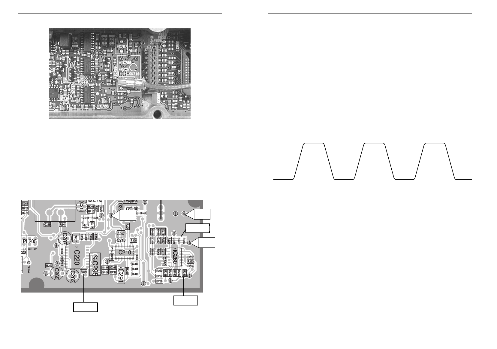
range with a second Micromatch socket can be fitted.)
4. Remove R291, R289, and R296 from the audio processor
(shown in Figure 2).
Figure 2 T800 Transmitter Audio Processor (older version without Micromatch connector) - Top Side
R291
S6
S7
S5
R289
R296
4. Using an AC-coupled oscilloscope set to 50 mV/div, observe the signal
at TP2. Adjust RV2 until the triangle wave amplitude has been mini-
mised.
5. Apply 600 Hz to the DATA line. Use a modulation analyser to observe
the frequency deviation on the output of the transmitter. Adjust RV1 to
get 4.5 kHz deviation on the modulation analyser.
6. Observe the transmitter’s VCO control line using an AC-coupled oscil-
loscope set to at least 20 mV/div and 0.5ms/div. Vary the input fre-
quency down to low frequencies (for example 100 Hz) and check that
the control line still has a good square wave.
Note: You may have to re-adjust RV2 and RV1 alternately to achieve a square wave
on the VCO control line and a 4.5 kHz deviation. Figure 7 shows a typical 100
Hz VCO control line waveform with RV1 and RV2 set correctly.
Figure 7 100 Hz VCO Control Line Waveform
Note: If the lower cut off frequency of an AC coupled oscilloscope is too high,
excessive distortion may be introduced which will result in 'sag' on the square
wave displayed. Determine if this is a problem by directly monitoring the
original square wave source and observe any sag.
If there is sag, switch the oscilloscope to DC and use a 10µF capacitor in
series with the scope probe (observing the correct polarity) to directly monitor
the VCO control line. Note that the trace settling time will be approximately
one minute.
6T800-32-0010 Fitting Instructions 419-83210-00 419-83210-00 T800-32-0010 Fitting Instructions 3
Figure 6 shows the location of these resistors on the PCB.
Figure 6 Location of Zero Ohm Resistors
For a different frequency, calculate the resistor pattern as follows:
1. Divide the external oscillator frequency by 100 kHz.
2. Convert the result into binary.
3. Where there is a 0 in the binary number, place a zero ohm resistor in
the equivalent position. Where there is a 1, leave an open link.
Modulation Adjustment
Before the paging transmitter can be used, its modulation must be set up cor-
rectly.
1. Apply +5 V DC to the DATA input (see Figure 8 for D-range 2 pin
assignments) and observe the transmitter output using a frequency
counter. The output should read the carrier frequency.
2. Remove the +5 V DC from the DATA input and apply a ground ( 0 V)
to the DATA input. Observe the transmitter output with a frequency
counter. Adjust RV3 to get an output of Fcarrier + 4.5 kHz.
3. Remove the 0 V from the DATA line and apply a 100 Hz 5 Vp-p square
wave.
MSB LSB
N7 N6 N5 N4 N3 N2 N1 N0
R92 R93 R94 R95 R96 R97 R98 R99
RV3
92
IC 14
TP2
99
98
97
96
939495
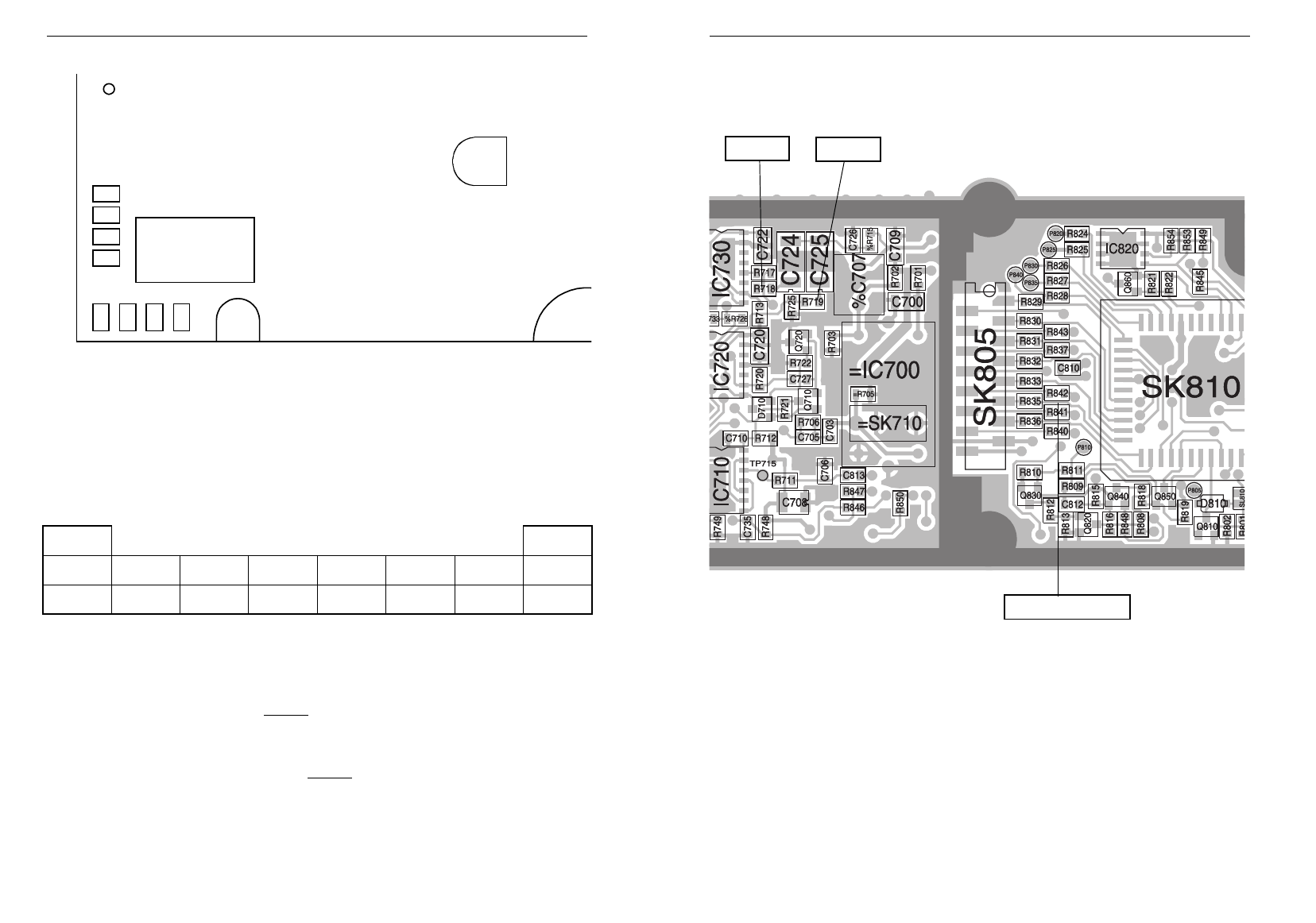
5. Remove R718 and R719 from the synthesiser compartment (shown in
Figure 3).
Figure 3 T800 Transmitter Microntroller and Synthesiser Compartments
6. Remove R841 and R842 (SMD) from the microcontroller compartment
(shown in Figure 3) to disconnect the appropriate lines from the micro-
controller.
7. Lay the T800-32-0010 PCB above the exciter compartment with the
component side up and positioned so that the Micromatch sockets are
on the side closer to the front panel of the radio.
8. Connect the 8-way ribbon cable to the SK200 Micromatch socket in the
audio compartment and connect the other end to the Micromatch
socket SK3 on the PCB.
R718 R719
R841 & R842
4T800-32-0010 Fitting Instructions 419-83210-00 419-83210-00 T800-32-0010 Fitting Instructions 5
If there is no Micromatch socket in the audio compartment (older
Series II transmitters), connect wires from the PCB to the audio com-
partment as follows.
For more information, refer to Figure 2 and the Test Points and Options
Connections drawing in the relevant service manual)
9. Connect the 4-way ribbon cable to the Micromatch socket SK4 and feed
it through the loom channel cast into the chassis, to the auxiliary D-
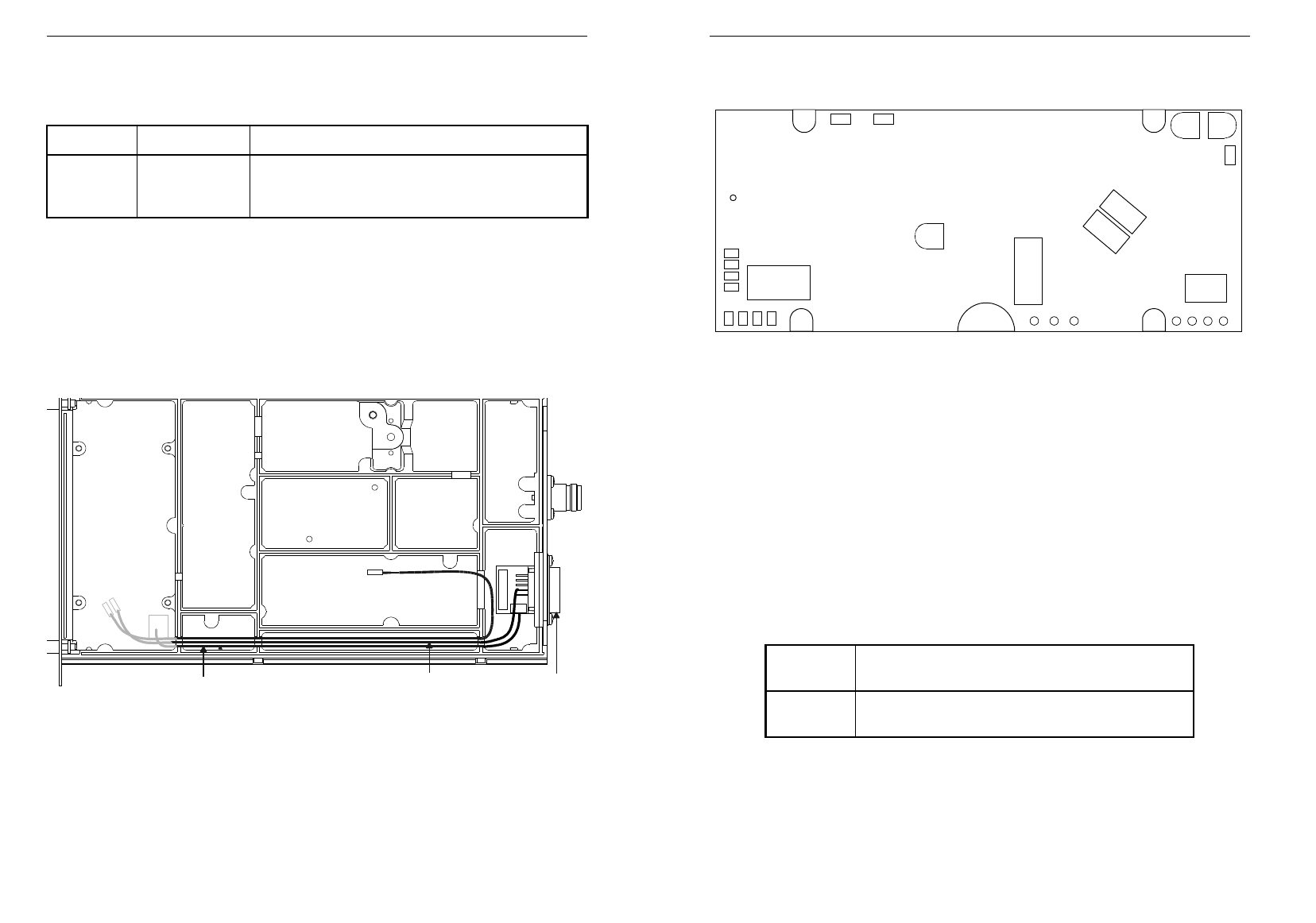
range compartment, as shown in Figure 4.
10. Connect the coaxial cable provided between SK1 on the T800-32-0010
PCB and =SK710 on the T800 transmitter PCB, as shown in Figure 4.
Figure 4 Cable Routing
11. Screw D-range 2 in place.
12. Thread the second coaxial cable from D-range 2 through the loom
channel to the paging board and connect it to SK2.
13. If the transmitter will be operating in VHF (frequencies <360 MHz),
solder short LINK2 and LINK 3 (see Figure 5).
(The T800-32-0010 PCB links are set for UHF operation.)
Figure 5 T800-32-0010 Link Location - Top Side
14. Turn the T800-32-0010 PCB over, so that the ribbon cables and compo-
nents face down, and position it above the audio processor compart-
ment.
15. Connect the other end of the 4-way ribbon cable to the Micromatch
socket on the auxiliary D-range.
16. Screw the PCB in place using the 4 M3 x 8 screws provided.
Configuring for the External Oscillator Frequency
The PCB is configured for a 10 MHz external reference, using a pattern of
zero ohm resistors. For a 5 MHz or 12.8 MHz external oscillator frequency,
you need the following pattern:
Wire Length (mm) Connection
red
grey
black
140
140
140
S5 I/O Pad, P240 (+9V) just below D230
S7 I/O Pad, P271 (BUFF_IN)
S6 I/O Pad, P261 (GND)
First coaxial cable
4-way ribbon cable
SK1 SK4
Auxiliary
D-range
(D-range 2)
SK2
Second coaxial cable
Reference
Frequency Resistors
5 MHz
12.8 MHz
R92, R93, R96, R97, R99
R93, R94, R95, R96, R97, R98, R99
RV2RV1
SK4
SK3
LINK2 LINK3
S7S6S5 S2S1S3S4
RV3
SK1
SK2
LINK1
92
IC 14
TP2
99
98
97
96
939495