Tektronix Water Dispenser 494A Users Manual
494A to the manual 67a0ebf2-7266-4669-9a5c-00505daf38a6
2015-02-03
: Tektronix Tektronix-Water-Dispenser-494A-Users-Manual-464251 tektronix-water-dispenser-494a-users-manual-464251 tektronix pdf
Open the PDF directly: View PDF ![]() .
.
Page Count: 336 [warning: Documents this large are best viewed by clicking the View PDF Link!]
Service
Manual
494A
& 494AP
Tektronix
o
o
o
o
o
o
o
o
o
o
o
I
o
o
o
o
a
o
o
o
o
o
o
o
o
o
o
o
o
o
o
a
o
o
a
o
o
o
o
o
o
o
o
o
Spectrum
Analyzers
Volume 1
070-ss60-00
Warning
The servicing
instructions
are for use
by qualified
personnel
only. To avoid personal
injury, do not
perform any
servicing unless
you are
qualified to
do so. Refer to the Safety
Summary
prior to
performing
service.
Please
check for change information at the rear
of this manual.
First
Edition:
January
1
987
Copyright @
Tekrronix, Inc. 1987.
All rights reserved.
Tektronix products
are covered by U.S. and foreign patents,
issued
and pending. Information in this publication supercedes
that in all previously published material. Specifications and price change
privileges reserved.
Printed
in the
U.S.A.
Tektronix,
Inc., P.O. Box 1000,
Wilsonville, OR 97070_1000
TEKTRONIX and TEK are registered
trademarks
of Tektronix. Inc.
I
o
o
o
?
o
a
o
o
t
o
o
O
o
o
o
o
a
o
o
o
o
o
o
o
o
o
o
o
o
o
a
o
o
o
o
a
o
o
o
o
a
o
o
o
o
o
o
o
o
o
o
o
o
a
o
I
o
o
O
o
o
o
o
o
o
o
o
o
o
o
O
I
o
o
o
o
o
o
t
o
o
o
o
I
O
a
o
RELEASE
OF COPYRIGHT
Tektronix
cannot
provide
manuals
for
measurement
products
that are
no
longer
eligible for
long
term
support.
Tektronix
hereby
grants permission
and license
for
others
to reproduce
and distribute copies
of any
Tektronix
measurement
product
manual,
including
user manuals, operato/s
manuals,
service
manuals,
and the
like,
that
(a)
have
a Tektronix
part
Number
and
(b)
are for
a measurement product
that is no longer
supported
by
Tektronix.
A Tektronix
manual may be
revised to reflect
changes
made
to the
product
during
its manufacturing
life. Thus,
different
versions
of a manual may
exist for any
given
produot.
Gare
should
be
taken
to ensure
that
one
obtains the
proper
manual
version for
a specific
product
serial number.
This
permission
and license
does not
apply
to
any
manual
or
other
publication
that
is still available from
Tektronix,
or to
any
manual
or other
publication
for
a video
production
product
or a color
printer
product.
Tektronix
does not
wanant the
accuracy
or
completeness
of the information,
text,
graphics,
schematics,
parts
lists,
or other
material
contained
within
any measurement
product
manual
or other
publication
that is not
supplied by
Tektronix or that is
produced
or distributed
in
accordance
with
the
permission
and
license
set
forth
above.
TEKTRONIX
SHALL
NoT BE LIABLE
FoR
ANY
DAMAGES
WHATSOEVER
(|NCLUD|NG,
WTTHOUT
LtMtTATtON, ANy
CONSEQUENTIAL
OR
INCIDENTAL
DAMAGES,
DAMAGES
FOR
LOSS
OF
PROFITS,
BUSINESS
INTERRUPTION.
OR
FOR
TNFRTNGEMENT
OF TNTELLECTUAL
pROpERTyl
AR|S|NG
OUT
OF
THE
USE
OF ANY
MEASUREMENT
PRODUCT
MANUAL OR OTHER
PUBLICATION
PRODUCED
OR
DISTRIBUTED IN
ACCORDANCE
WITH
THE PERMISSION
AND LICENSE
SET
FORTH
ABOVE
Thomas
F.
Lenihan
Chief
tntellectual
Property
CounselTektronix,
tnc
(503)
627-7266

o
a
o
o
,.'.t
a
o
a
o
a
a
o
o
o
t
a
a
o
I
o
o
o
o
o
o
o
O
a
I
o
a
o
a
o
o
t
a
o
o
a
a
a
a
a
I
o
o
I
o
I
t
I
o
o
I
I
O
o
I
t
o
I
I
o
o
o
o
o
o
o
t
o
I
o
o
o
o
o
I
o
O
t
I
O
o
O
t
o
WARRANTY
Tektronix warrants that this product will be free from defects
in materials and workmanship fbr a period of one (l)
year from the date of shipment. If any such product proves
defective during this warranty feriod, Tektronix, at its
option, either will repair the defective product without charge for parts and labor, or will provide a replacement
in
exchange
for the defective product.
In order to obtain service under this warranty,
Customer
must notify Tektronix of the defect before the expiration
of the warranty period and make suitable arrangements
for the performance of service.
Customer shall be
responsible
for packaging and shipping the defective product to the service center
designated
by Tektronix, with
shipping charges
prepaid-
Tektronix shall pay for the return of the product to Cusromer
if the shipment is to a
location
within the
country
in which the Tektronix
service
center
is located.
customer
shall
be responsible
for
paying all shipping charges,
duties, taxes,
and any other charges
for products
returned
to any other locations.
This warranty shall not apply to any defect, failure or damage
caused
by improper use
or improper or inadequate
maintenance
and care' Tektronix shall not be obligated to furnish service under this warranry a) to repair damage
resulting from attempts
by personnel
other than Tektroriix representatives
to install, repair or service the product;
b) to repair
damage
resulting
from improper
use
or connection
to incompatible
equipment;
or c) to service
a
product that has
been modified or integrated
with other products when the effect of such
modification or
integration increases
the time or difficulty of servicing the product.
TIIIS WARRANTY IS GIVEN BY TEKTRONTX WITH RESPECT TO THIS PRODUCT IN LIEU OF
ANY OTI{ER WARRANTIES, EXPRESSED OR IMPLIED. TEKTRONIX AND ITS VENDORS
DISCLAIM ANY IMPLIED WARRANTIES OF MERCHANTABILITY OR FITNESS FOR A
PARTICULAR PURPOSE. TEKTRONIX'RESPONSIBILITY TO REPAIR OR REPLACE DEFECTIVE
PRODUCTS IS THE SOLE AND EXCLUSIVE REMEDY PROVIDED TO THE CUSTOMER FOR
BREACH OF THIS WARRANTY. TEKTRONIX AND ITS VENDORS WILL NOT BE LIABLE FOR ANY
INDIRECT' SPECIAL, INCIDENTAL, OR CONSEQUENTIAL DAMAGES IRRESPECTIVE OF
WHETHER TEKTRONIX OR THE VENDOR HAS ADVANCE NOTICE OF TIM POSSIBILITY OF
SUCH DAMAGES.

O
a
o
I
?
o
a
a
a
a
a
I
t
o
I
a
a
a
O
o
O
o
o
o
t
C
a
I
a
o
O
t
a
o
a
o
a
o
o
a
o
o
I
o
o
o
o
t
o
o
I
I
o
a
O
I
a
o
I
I
o
t
I
o
a
o
O
o
I
o
o
o
I
o
o
I
o
o
o
a
o
I
a
o
o
o
o
o
PREFACE
This manual
contains servic€
information
for the
TEKTRONfX
494A1494Ap.
The information
is tocated
in
two volumes.
Volume
1 contains
the
text and
Volume
2
contains
the diagrams
and parts lists. The Tabte
of
Contents
in each volume lists the contents
of both
volumes.
Manuals
that describe
other
aspects
of the
product
are:
. Operator's
Manual
. Operator's
Handbook
o Programmer's
Manual
o Programmer's
Reference
Guide
Who Should
Use This Manual?
This
rnanual
is intended
for electronic
technicians
with
experience
in servicing
digital,
analog,
and
rf circu-
itw. Circuit
analysis
is mostly
functionil and shoutd
help isolate
most malfunctione
to a board
or block
of
circuitry.
The technician
should
then be abte,
with the
aid of test equipment,
to isolate
the malfunction
to a
specific
component
or components.
This instrument
contains
firmware
that provides
a
thorough instrument
check
during power
up and
during
operation,
and if needed,
guides
the usei
through
ai
abbreviated
front-panel
calibration
procedure.
lf cali_
bration
cannot
be achieved,
a diagnostic
test
detects
and
isolates
most problems
to the
system,
such
as 1st
LO. The
technician
can
then run
troubleshooting
diag-
nostics
to further
isolate
the problem
to the board
or
block of
components.
Refer
to the
Maintenance
section
for
diagnostics
information.
Documentation
Standards
Most
terminology
and graphics
follow
ANSI
stan_
qalds. A glossary
of terms
is provided
as
an
appendix.
Refer
to
the
following
standards:
494A/494AP
Service Vot.
1
. ANSI
Y1.1
- Abbreviations
. ANSI Y32.2
- Graphic
Symbots
o IEEE
91
- Logic
Symbots
Change/History
Inf
ormation
Sometimes
instrument
changes
occur or manual
errors
are found
that make
some of the information
in
the manual
inaccurate.
When
that happens,
Manual
Change
Information
notices
are inserted
at the rear
of
the
manual.
This helps
ensure
that the
manual
contains
the latest
and
most accurate
information
available
when
the
product
is sold.
History information,
with the updated data, is
integrated
into
the text or diagrams:
When
a text
page
is updated,
the revised pages
are identified
by a revi-
sion
date in
the
lower
inside corner
of the
page.
When
a diagram
is updated,
the revision
date is placed
at
the
lower center of the diagram. History information
is
shown
with a gray tint. When a component
value
is
changed,
the
designator on
the drawing
is boxed with
a
grey
outline.
When
a circuit
is deleted
or changed,
the
original
configuration
is shown
in grey,
drawn either
at
its
original
location
or
to the
side
of
the
drawing.
lf you
have a manual
other
than
the
one
that
came
with your
instrument
it may contain revisions
that do not
apply
to your
instrument;
however
all
history
informa-
tion
that
pertains
to the
earlier instruments
is retained.
When a major modification
has been made to an
assembly
or circuit
board, the data for the replaced
assernbly
will follow
the new information
and
will
be
identified
with appropriate
titles
or headings such
as
instrurnent
serial
number range
or the assembly
or
board
part
numbers.
Also, if your
instrument
has an assembly replaced
with a newer version,
documentation
for the newer
assembly
may
be supplied.
Contact
any
Tektronix
Ser-
vice
Center for information.

o
o
o
I
a
o
t
a
a
a
o
a
o
o
I
O
a
a
a
o
o
o
o
o
o
o
t
o
a
a
o
o
I
o
o
o
a
o
o
o
a
o
a
o
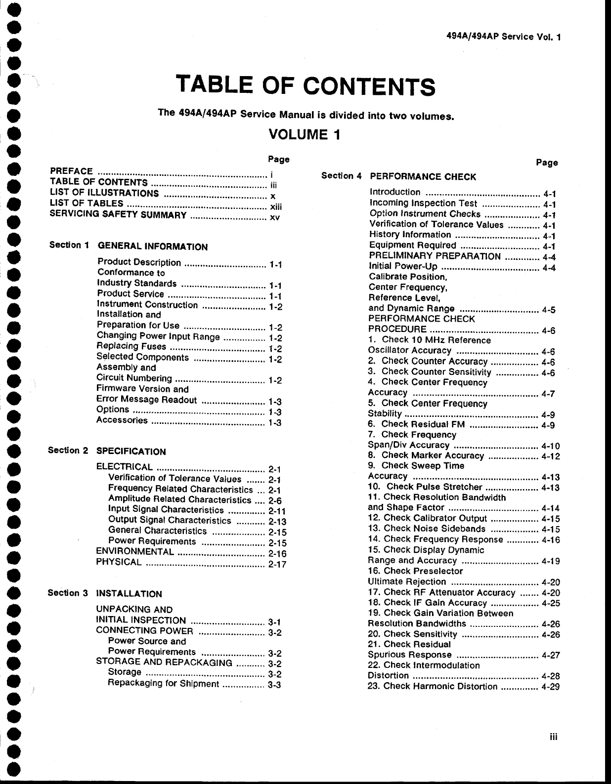
TABLE
OF
CONTENTS
The
494A/494AP
service
Manuat
is divided
into two volumes.
VOLUME
1
Page
PREFACE ........................
i
TABLE
OF
CONTENTS
.............. ..........
iii
LIST
OF ILLUSTRATTONS
........... ........
x
LIST
OF TABLES .............
xiii
SERVICING
SAFETY
SUMMARY .........
xv
Section
1 GENERAL
INFoRMATION
product
Description ...........
1_1
Conformance
to
Industry
Standards ............
1_1
Product
Service .................
1_1
Instrum€nt
Construction ....
1-z
Installation
and
Preparation
for
Use ...........
,l_2
Changing
power
Input
Range
....,.....,.....
1_2
Replacing
Fuses
.........
Selected
Components .......1-2
Assembly
and
Circuit
Numbering ..............
1_2
Firmware
Version
and
Error
Message
Readout ....
1-g
Options ..........
1-g
Accessories ..,....................
1-3
Section2 SPEC|F|CAT|ON
ELECTRICAL
................ .....2-1
Verification
of
Tolerance
Values
.....,.
Z-1
Frequency
Related
Characteristics
...
2-1
Amplitude
Related
Characteristics
....
2_6
Input
Signat
Characteristics
..............
2-1
1
Output
Signal
Characteristics
...........
2-1g
General
Characteristics
....................
2-1
s
' Power
Requirements
........,.........,.....
2-1 5
ENV|RONMENTAL.......... ...
2_16
PHYSTCAL .....2-.t7
Section
3 INSTALLATION
o
o
o
t
o
o
o
o
o
o
o
a
I
o
I
a
a
o
I
o
o
o
o
o
o
o
o
o
t
o
a
o
I
o
o
t
o
I
a
o
o
a
o
o
UNPACKING
AND
tNtilAL
TNSPECTTON .......,
3-1
coNNECTtNG
POWER .....
3_2
Power
Source
and
Power
Requirements
........................
g_2
STORAGE
AND
REPACKAGING
......,....
3.2
Storage .....
g_2
Repackaging
for
Shipment
................
g-3
494A/494AP
Service
Vot.
1
Page
Section
4 PERFORMANCE
CHECK
Introduction ..,.4-1
Incoming
Inspection
Test
......................
4_1
Option Instrument
Checks
..............,......
4_1
Verification
of Tolerance
Values
............
4_1
History Information ............
4-1
Equipment
Required ..........
4-1
PRELIMINARY
PREPARATTON
.............
4-4
Initial Power-Up
............ .....44
Calibrate
Position,
Center
Frequency,
Reference
Level,
and Dynamic
Range ..........
4-s
PERFORMANCE
CHECK
pRocEDURE
................ .....
4_6
1. Check't0
MHz Reference
Oscillator
Accuracy ...........
4_6
2. Check
Counter Accuracy
..................
4-6
3. Check
Counter Sensitivity
................
4-6
4. Check
CentEr Frequency
Accuracy .,......4-T
5. Check
Center
Frequency
Stability ...........
4-9
6. Check
Residual
FM
..........................
4-9
7. Check
Frequency
Span/Div
Accuracy ............
4-10
8. Check
MarkerAccuracy
...................
4-12
9. Check
Sweep
Time
Accuracy ........4-19
10. Check
Pulse
Stretcher
....................
4-19
11.
Check
Resolution Bandwidth
and
Shape Factor ..........-...4-14
12.
Check
Calibrator
Output
.................. 4-15
13.
Check
Noise
Sidebands
..................
4-15
14.
Check
Frequency Response
............
4-16
15.
Check
Disptay Dynamic
Range and
Accuracy .............................
4-1
g
16.
Check Preselector
Ultimate Rejection .........-...4-20
17.
Check
RF Attenuator
Accuracy
....... 4-20
18.
Check lF
Gain
Accuracy
..................
4-25
'l
9. Gheck
Gain
Variation
Between
Resolution
Bandwidths ......4-26
20.
Check
Sensitivity ......... 4-26
21. Check
Residual
Spurious Response ...........4-27
22. Cheek
lntermodulation
Distortion ........4-2A
23.
Check
Harmonic Distortion
........,..... 4-29
ill

o
o
o
I
.|
r
o
o
a
a
o
I
o
o
t
a
o
O
o
o
o
I
a
o
o
o
t
o
a
a
I
I
I
o
o
o
o
o
I
o
a
a
a
o
tv
49441494AP
Servtce
Vot.
i
Section 4
Section 5
TABLE
OF
CONTENTS
(Gonr.)
page
PERFORMANCE
CHECK
(Conr.)
24.
Check LO
Emission .....4-29
25.
Check 1
dB
Compression
point
.......4-29
26.
Check External
Reference
Input
Power .... 4-31
27.
Check
Triggering
Operation
and
Sensitivity
.............. ..... 4-31
28.
Check
External
Sweep
Operation ...............
4-92
29.
Check
VERT
OUTPUT
Signat
..........
4-34
30.
Check
HORTZ
OUTPUT
Signaf
Level ....4-94
oPTloN
TNSTRUMENTS
.......................
4_34
31.
Check
Option
07
Calibrator
Output ...............
4-94
32.
Check
Option
07
Frequency
Response ......... 4-95
33.
Check
Option
4i Frequency
Span/Div
Accuracy ............
4-gz
34.
Check
Option
42
110
MHz
OUT Level ..........
4-gB
35.
Gheck
Optiopn
42110
MHz
tF
Output
Bandwidth,
Center Frequency,
Bandpass
Ripple,
and
Symmetry
About
110
MHz ..................4-gg
GPIB
VERIFICATTON
PROGRAM
..........
4-39
ADJUSTMENT
Introduction ....
5-1
Equipment
Required ..........
5-1
ADJUSTMENT
PROCEDURE
................
5-2
PREPARAT|ON
............. .....5-2
1. Adjust
Low
Voltage
power
Suppty
... 5-3
2. Adjust
Z-Axis
and
High
Voltage
Circuits .........
5-5
3. Adjust
Deflection
Amptifier
Gain
and
Frequency
Response
.............
5-6
4. Adjust
Digital
Storage
Calibration
....
5-g
5. Adjust
Sweep
Timing ....
5-g
6. Adjust
Frequency
Gontrol
System
and
Dot
Marker
Position ....
S-g
7. Adjust
Log
Amplifier
.........................
5-11
8. Adjust
Resolution
Bandwidth
and
Shape Factor ..............
5-14
9. Preset
the Variable
Resolution
Gain
and Band
Leveling
.....,..................
5-19
10. Adjust
Calibrator
Output Levet
........
5-20
11. Adjust
lF
Gain ..............
S-20
12. Adjust
B-SAVE
A
Refergnce
Level
......... .......5-21
13.
Adjust
Preselector
Driver ................
S-21
14.
Adjust
Band
Leveling
for
Coaxial
Bands ...................
5-24
Section 6
Page
15. Adjust
Band
Leveling for
Waveguide
Bands ..............
5-25
16. PhasE
Lock
Calibration ....................
5-2S
OPTION INSTRUMENTS
ONLY .............
5-29
17.
Adjust
Option 07
VR Band Leveling 5-29
18. Adjust
Option 42 Module
.................
5-29
MAINTENANCE
TNTRODUCTTON
...............................
6-1
Removing
the
lnstrument
from its
Cabinet
..........
6-1
static-sensitive
components .......
6-1
PREVENTIVE
MAINTENANCE
...............
6.2
Elapsed Time
Meter
.....................
6-2
Cleaning ......-............
6-2
Lubrication ...............
6-2
Fixtures and
Tools
for Maintenance
.................,.........
6-2
Visual lnspection
..........................
6-2
Transistor and Integrated
Circuit Checks ..........
6-2
Performance
Checks
and Recalibration
.........................
6-3
Saving Stored Data
in
Battery-Backup
Memory
...............
6-3
TROUBLESHOONNG ........6.3
Troubleshooting
Aids ...................
6-9
Diagrams .............
6-3
Circuit
Board
lllustrations and
Component
Locator Charts .....
6-4
Diagnostics ..........
6-4
General
Troubleshooting
Techniques ...............
6-4
Semiconductor Checks
............
6-4
Diode
Checks
..........................
6-4
Diagnostic Firmware
................,...
6-5
Troubleshooting
Steps
.................
6-5
DTAGNOSTTCS
......................................
6-5
TROUBLESHOOTING
USING
THE
ERROR
MESSAGE DISPLAY
.... 6.5
Introduction ..............6-5
Combination of Error
Messages
...
6-6
Procedure Format .... 6-6
TRACE MODES ............
6-14
Alternate Frequency Display
........
6-14
Auxiliary Synthesizer Control .......
6-14
Correction
Disable/Enable ........-...
6-14
coRRECTtVE MATNTENANCE ..............
6-15
Handling Static
Sensitive
Components .............6-1
5
Obtaining
Replacement Parts .......
6-1
5
Parts
Repair
and Return
Program ...................
6-1
5
TABLE
OF
CONTENTS
(Conr.)
o
o
o
I
O
I
I
o
o
O
I
a
o
o
a
I
o
I
o
o
t
o
o
o
a
o
o
o
I
o
a
a
t
o
O
o
I
o
o
o
a
o
o
o
494A/494AP
Service
Vot.
1
Section
6
page
MAINTENANCE
(Conr)
Firmware
Version
and
Enor
Message
Readout
...............
6-1
5
Selected
Components
..................
6-1
5
Replacing
EPROM
or
ROM
Devices ........
6-15
Surface-Mounted
Components
.....
6_1
6
Replacing
Surface-Mount€d
Components ..............
6_17
Transistor
and
Integrated
Circuit
Configurations
................,..
6_1
7
Diode
Cotor
Code .........................
6_1
g
Multiple
Terminal
(Harmonica)
Connectors
...............
6_1
g
Resistor
Values .........
6-1g
Capacitor
Marking .....
6_1g
Soldering
Techniques
...................
6-1
g
Replacing
the
Square
pin for
the
Multi-pin
Connectors
..............
6_1g
Servicing
the VR
Module
..............
6-1g
REPLACING
ASSEMELIES
AND
SUBASSEMBLTES
....................
6_19
Removing
and
Installing
the
GPIB
Board .........6-22
Removing
or Replacing
Semi-rigid
Coaxial
Cables
............
6_22
Replacing
the Dual
Diode
Assembty
in
the 1st
Mixer
............
6_22
Replaeing
the
Crt ......
6_23
Repairing
the
Crt
Trace
Rotation
Coil ...
6-29
Front
Panel
Assembly
Removal
...6-29
Front-Panel
Board
Removal
.........
6_24
Replacing
Front
panel
Pushbutton
Switches
....................
6_24
Main
Power
Suppty
Module
Removal ........
6_24
High
Vottage
power
Supply
..........
6_25
Removing
and
Replacing
the
lst
LO ..6_25
Replacing
the
l st LO
Interface
Board .........
6_25
Fan
Assembty
Rernovaf
................
6-25
MAINTENANCE
ADJUSTMENTS
......
6.26
110
MHz
tF
Assembty
Return
Loss
Calibration
................
6-26
2072MHz
2nd
Converter
.............
6_26
Four
Cavity
Filter
..........
...........
6_27
Mixer......... ...........,9-27
110
MHz
Three
Cavity
Fitter
.........
6_29
829 MHz
Converter
Maintenance ..............
6_29
Troubleshooting
and
Calibrating
the 2nd
LO ............. ..6-32
Page
Preparing
the
2nd
LO
Assembly
for
Adjustment
.............
6-35
Reassembling
the
2nd LO
Assembty .....
6-9g
Troubleshooting
and
Calibrating
the 16-20 MHz Phase
Lock
Section .....................
6-40
Troubleshooting
Aids
for
the
2182MHz
Phase
Locked
2nd
LO Assembty .....6-42
100
MHz
Osciltator
in the
3rd Converter
...............................
649
l st
Converter
Bias .....................,.
6-44
Auxiliary
Synthesizer
VCO
Adjustment
...........................
6-44
Baseline
Leveling
(Video
Processor) .....
6-46
10 MHz
Reference
Oscillator
Accuracy .. 6-49
MICROCOMPUTER
SYSTEM
MATNTENANCE
............. ....
6-50
Option
Switches .......
6-50
Power-up
Self Test ...
6-50
Microcomputer
System Test ........
6-51
Address
Bus
Test .....
6-52
Microcomputer
Bus .................
6-52
Mernory
Address
Decoders
.....
6-52
Processor
Address
Decoder
....
6-59
GPIB Board
Address
Decoders
Clocks ahd
Control Lines
.........
Instrument
Bus
Test
TROUBLESHOOTING
ON THE
INSTRUMENT
BUS
Instrument Bus
Data
Transfers
....
Instrument
Bus Registers,............
Front-Panel
Registers
TAPE OATA
TRANSFER
PROGRAM
....
THEORY
OF OPERATION
FUNCTTONAL
DESCR|pTtON
............
.... 7
-1
What
lt Does
................-...........
7-1
How
lt Works .......7-1
First,
Second, and
Third
Gonverters ...........
........... 7
-1
lF
Section ..-.........7-2
Display
Section ....7-2
Frequency
Control
Section .,....
7-2
Counter and
Phase
Lock
Section .............,...
7-2
Digital
Control Section
............. 7-3
Power
Supply
Section ..............
7-3
Other
Sections
...............
.......... 7-3
6-s3
6-54
6-54
6-54
6-54
6-56
6-62
6-63
Section 7
TABLE
OF
CONTENTS
(Cont.)
Page
Section 7 THEORY
OF OPERATTON
(Cont)
DETAILED
DESCR|PT|ON
................
.....
7
-4
1ST
CONVERTER
SECTTON
.............
7_4
RF Interface
Qircuits
....................
7-4
'l
st
Converter
.................
..........,,,..
7-4
RF
Input ...............
7-4
Preselector
Circuits ...........,.....
74
lst Mixer ..............
7_5
1st
Local
Oscillator
..................
7_5
power
Divider ......
7-s
Transfer
Switch .... 7-s
Directional
Filter
................,......
Z-6
2O72MHz
tF
Fitters
....,............
7-6
Diplexer
and
Filter
...,...............
Z-6
2ND
CONVERTER
SECTTON
............
7_7
2072
MHz 2ND
CONVERTER
.......
7-8
Four-Cavity
Fi|ter
.......... ...........
Z
-g
Mixer
Circuit
............................
7-g
Precision
External
Cables
........
7-9
Filter
to Mixer
RF
Input
Gable
....................
7-10
2nd LO
to Mixer
LO
Input
Cable
....................
Z-10
2182MHz
PHASE
LocKED
2ND
LO .....................7-10
2182MHz
Microstrip
Oscillator .............
7-10
2200
MHz Reference
Board ....................7-11
220O
MHz Reference
Mixer ......... ...........7-11
16-20
MHz
phaselock
Board ....................7-11
829
MHz 2ND
CONVERTER
.........7-19
lF
Section ............
7,13
829
MHz
Diplexer
.,..............
7-t
g
829
MHz
Amplifier
...............
t-13
829 MHz
2nd
Converter
...,..7-14
110
MHz lF
Se|ect...............
7-i5
LO
Section ...........
7-16
Phase
Lock
Circuit ..............
7-16
2nd
Local
Oscillator
Ouput Circuit ... 7-19
719
MHz
Output
Circuit
.......
7-18
3RD
CONVERTER
SECTION
......,.....
7-19
110
MHz tF
AMpLtFtER
...............
7-19
110
MHz
FILTERS
3rd
CONVERTER
............ ..............
7
-2A
100
MHz
Oscillator
..................
7_20
Mixer......... ...........
7_20
Distribution
Amplifier
...............
7
-20
Calibrator .............2-21
REFERENCE
LOCK
......,...............
7-21
External
Referance
Det€ctor ...,...,,..,...7-21
Page
Frequency
Synchronizer ..........
7-21
Phase/Frequency
Detector ...,.,..,.....,7-21
Tune Amplifi
er
...............
........... 7-22
Lock Detector ..............
.........
"..
7
-22
rF
sEcTtoN ...................7-22
VAR|ABLE
RESOLUTION
............. 7-22
VR
fnput ...............7-22
1st Filter
Select .....7-22
100 Hz and 10 Hz
Bandpass
Filter
..........
.............. 7
-24
1st Mixer ,..,,.....7-25
Bandpass
Filter
..........
....,.,..
7
-25
2nd Mixer .........7-25
Local
Oscillator .............
......
7-26
10
dB Gain Steps ..........-..........7-26
20
dB Gain Steps .....................7-26
Band
Leveling
Circuit ........,...... 7-27
VR
Mother Boards ................... 7
-27
2nd
Filter
Select ....7-28
Post
VR Amplifier
Circuit
.........7-28
LOG
AMP
and
DETEGTOR
.......... 7-29
Log Amplifier Circuits .............. 7-29
Detector
Circuit .-...7-31
DTSPLAY
SECTTON ........7€3
FUNCTIONAL
DESCRIPTION ....... 7-33
VIDEO
AMPLIFIER .,,.7.33
Log Mode
Circuits
................... 7-33
Linear
Mode Circuits ..............-.
7-34
Pulse
Stretch Circuit
................ 7-34
ldentify
Circuit .......
7-35
Digital
Control
Circuit ...............
7-35
vrDEo
pRocESSoR
.................... 7-35
Interface
with
1405 TV
Sideband
Adapter .............-...... 7-35
Mdeo Marker ...........................
7-36
Video
Leveling .......,...... ...........
7
-37
Video
Leveler
Circuits .............. 7€7
Video
Filter Circuits ......,..........
7-37
Video
Blanking
.-..............,........ 7-39
DIGITAL STORAGE 7-39
Verticaf
Section .....740
Digitizing Circuits ................ 743
Address Decoding ............... 7-43
Interface
Logic ......... ..,........
743
Maximum
Hold .................... 743
Constant Circuit
..................
7-43
Output Circuits
....................
7-44
Peak/Average
Level
Circuits .............7-44
Horizontal
Section
.....-.............
7-44
Marker lC ............................ 7-46
Tracking Digital-to-
Analog
Converter ................
7*46
Update
Marker
Circuits .......746
a
o
o
o
't
o
o
a
a
a
o
o
o
a
o
o
t
o
o
I
o
I
o
o
o
o
o
o
o
o
o
t
o
o
o
o
o
a
o
o
o
o
o
o
494A1494AP
Servlce
Vol. 1
vl
TABLE
OF
CONTENTS
(Conr.)
o
o
o
o
o
o
O
a
o
o
o
a
o
I
t
I
o
I
o
o
I
o
o
a
o
o
o
o
o
t
o
a
I
o
o
t
t
o
a
O
o
o
o
a
494A1494AP
Service
Vot.
I
Page
Section
7 THEORY
OF
OPERATION
(Conr)
Fast
Retrace
Blanking
...,.,...
742
Memories ........7-47
DEFLECTION
AMPLIFIERS
..........
7-47
Horizontal
Section
...............,...
747
Vertical
Section ....249
Z.AXIS
AND
RF
INTERFACE
.......
7-48
RF
Interface
Circuits
................
7_49
Z-Axis
Circuits .....7_49
power-Fail
Detector
.................
7-50
power
Supply
Monitor
.............
7_50
Options
Switch .....
7-50
Timer
......... ..........
7_50
HIGH.VOLTAGE
SUPPLY
.............
7.50
High-Vottage
Osciilator
............
7-50
Voltage
Doubter ... 7_SO
High-Voltag€
Regulator
............
7_S0
Z_Axis
Gtipper ......
7_51
cRT READOUT
............................
7_51
Generating
Readout
.................
Z_51
R€adout
OnlOtr Timing
.......
Z-S1
Character
Scan ...................
7-Sj
Character
Generator
Timing .............
z-54
Dot
Defay .....-..2-54
lnstrument
Bus
Interface
.........
7-56
Control
Port
.........................
7-56
Address/Data
Port
...,...,......
T
-Sz
Frequency
Dot
Marker
.,...........
7_57
FREQUENCY
CONTROL
sEcTtoN .. 7_60
Sweep ..................
7-60
Span
Attenuator
.......................
Z-60
Center
Frequency
Control ........
7-60
1st
LO
Driver
...........................
7-60
preselector
Driver
....................
Z_60
swEEP .....................
7-60
Digital
Controt ......7_61
Sweep
Generator
.....................
7_62
Trigger
Circuits ....7-62
Sweep
Output
Circuits .............
7_62
Marker
DAC
.............................
7-63
Sweep
Control .....
Z_69
Trigger
Control
..................;.....
Z-69
Sweep
Holdoff .....7-64
Interface
Circuits .....................
7_64
spAN ATTENUATOR
...................
7-65
DigitalControl ......
7-65
lnput
Section ........
7_65
Digital-to-Analog
Converter
.....
7_65
Decade
Attenuator
...................
7_66
Page
lst LO DRIVER .........7-67
Digital
Controf ...... 7-6g
Input
Switching
........................
7-69
Oscillator Filter
Switch Driver .......7-69
Summing Amptifier
...................
7-69
Oscillator Driver ... 7-69
Reference
Suppty ....................
Z-69
Mixer Bias
Driver
.....................
7-69
Programmable
Bias
.................
7-69
PRESELECTOR
DRTVER
..............
7-69
Digitaf
Control
Circuits .............
7-70
Oscillator
Voltage
Processor
...
7-lO
lF
Offset ...............7-21
Summing Amplifi
er
...................
7
-71
Tracking
and
Shaper
Circuits ....7-71
Current
Driver ...... Z-72
Preselector
Switch
Driver
.,...... 7-22
CENTER FREQUENCY
CoNTROL -................7-72
Operating
Modes
.....................
7
-72
Digital Control ......7-73
Storage
Registers ..,..,.........
7-74
Digital-to-Analog
Converters .......7-75
Track-and-Hold
Amplifier ......... 7
-7
5
Write-Back
Circuit
........,...........
7-76
-1
0
V Reference
Buffer ......... ..7-76
COUNTER
and
PHASE
LOCK
sEcTroN ...7-77
FUNCTIONAL
DESCRIPTION ....... 7-77
Phase
Lock
Assembly ............. 7-77
Frequency
Gontrol
................... 7
-78
Controlling
the
Oscillator Frequency
......,.,.,
7
-78
Counting
the
lF .................... 7-78
HARMONIC
MIXER ..7.78
AUXILIARY
SYNTHESIZER
.......... 7-79
COUNTER
BOARD .,,7.82
Address Decoder
.....................
7-82
Service
Request
Circuits
......... 7-82
Data Buffers .........7-82
Input Amplifiers
and
Multiplexer ........... 7-83
+2n
Gounter .........
7.83
21
-bit
Counter ..........................
7-83
PHASE LOCK
SYNTHESIZER
...,..7.83
Synthesizer ..........
7-83
Phase Lock
.............................. 7-84
Offset
Mixer ........................ 7-84
Error
Amplifier
.....................
7-85
Controlled
Oscillator
............ 7-86
Strobe Driver
Circuit
............ 7-86
vll
TABLE
OF
CONTENTS
(Cont.)
Page
Section
7 THEORY
OF
OPERATTON
(Conr)
DtctTAL
CONTROL
SECTTON
.......... 7_88
Microcomputer
.............................
7-gg
Processor .............
7-gg
Microprocessor
...................
7-88
Cfock ......... ......7-92
Microcomputer
Bus
........,....
T-92
Address
Decoder
................
Z-92
Timer ......... ......7-gz
PIA and
lnstrument
Bus ...... 7-92
DMA
Controller
.............
......
7
-gz
Interrupt
Processing
...........:
7-93
Memory .................2-94
Address
Decoders
..............
7-94
RAM
.......... ......7-94
Options .............
7-95
ROM .......... ......7-96
ROM
Banks
and
GptB
.............
7-96
Address
Decoder
................
7-96
Bank
Selector
......................
7-96
Bank
ROMs .....
7-96
GPIB
Switches
...............,....
7-97
GPfA
.......... ......7-97
Accessoriss
Interface
.......,.,....
Z-gT
Front
panel ..........
7_97
Pot€ntiometers
....................
7-98
output Mode
shift
R€gisters
and
LEDs
............ 7-98
Processor ...,.... 7-98
Scanning the Keyboard
....... 7-98
Scanning
the FREQUENCY
ControlCoder .. 7-gg
Outputting
the
Correct
Code .......................
7-99
Software .......... 7-gg
Main
Scan
Routine
..............
7-99
Keyboard
Check
Subroutine .......7-100
Frequency
Coder
Subroutine
Check
................
7-1 00
Output
Subroutine
...............
7-100
Page
POWER
SUPPLY ..........7-103
Primary
Circuits ........
7-103
Line
Input
Circuits ....................
7-1 03
Invert€r Circuit ..... 7-103
Multivibrator ....
7-103
Ramp
Generator ..................
7-l
04
Primary
Regulator
...............
7-1 04
Inverter
Logic ......................
7-1
04
Inverter
Driver
.............,.......
7-1 05
Output Stage .............,.........
7-1 05
Soft Start
and Primary
Over-Current
Circuits ......"... 7-1 05
Secondary &
Fan Drive
Circuits ..... 7-106
Rectifi er-Filter Circuits ..................
7-1 06
*5V Voltage
Reference
Supply
Regulator
Circuits ..... 7-106
+5V Over-Voltage
Protection
Circuit ...... 7-106
Fan
Drive
Circuit -......7-107
Sectlon
8 OPTIONS
Options
A1-A5 Power
Cord Options ....
8-1
Option Bl Service
Manuals ...................
8-1
Options Ml-MS Extended Service
and Wananty
Options ........
8-1
Option
07
75O Input
..............................
8-2
Option 08 Delet€
External
Mixer Input ....8-2
Options 21 and 22
Waveguide Mixers .............
8-g
Option 39
Alternate Battery ...................
84
Option
41
Digital Radio .........................
8-4
Option
42110 MHz
lF Output
................
8-4
Option
45 MATECO ...........
8-4
Option
52 North American
220V ............
8-4
Appendlx A GLOSSARY
GENERAL
TERMS ........ A.1
FREQUENCY TERMS ... A-2
AMPLITUDE TERMS .....
A-2
DIGITAL
STORAGE
TERMS ..-.......... A-3
WAVEFORM
MARKER
TERMS ........ A-3
o
a
o
I
,a
o
o
a
o
a
I
o
t
o
t
a
o
o
I
a
a
o
o
o
o
a
o
t
a
o
I
o
o
o
I
o
o
I
o
O
o
o
o
4944/494AP
Servlce
Vot. 1
v||l
494A/{94AP
Service Vot.
1
TABLE
OF
CONTENTS
(Cont.)
VOLUME
2
Sec|ion
9 REPLACEABLE
ELECTRICAL
PARTS
Section
10 DTAGRAMS
Section
1.I REPLACEABLE
MECHANICAL
PARTS
494A/494AP
Servlce Vol. 1
Figure page
The 494AP
Spectrum
Analyzer.
...................
xvi
2-1 Dimensions. ....,....,..2-12
3-1 Location
of input
power
selector
switch
and fine
fuse.
.._....... .....,..,.........9-2
4-1 Crt
display at
initial
power-up.
......................
4-4
4-2 Typical
display of catibrator
signal
in Max
SpanlDiv.
...............................
4-5
4-3 Test
equipment
setup
lor checking
center
frequency
accuracy. ....... 4-g
44 Center frequency
drift with
the
1st
LO
tocked. ....................4-9
4-5 Typical
display
for measuring
residual
FM. ............ ..................4-10
4-6 Typical
marker
display for
measuring
Span/Div
accuracy.
.....................
4-1 1
4-7 Test
equipment
setup for checking
frequency
Span/Div and
sweep
Time/Div
accuracy. ....................
4-13
4-8 Typical
display
for measuring
Time/Div
accuracy. ....................
4-14
4-9 Typical
display
for measuring
bandwidth and
shape
factor. .....4-14
4-10 Typical
display
for measuring
noise sidebands.
........... ............ 4-15
4-1'l Test
equipment
s€tup tor
measuring
0.01
GHz to 21
GHz
frequency
response. ..................
4-17
4-12 Test equipment
setup
for
measuring
10
kHz
to
l0 MHz
frequency
response. ..................
4-19
4-13 Test
equipment
setup for
checking
dynamic range
and accuracy,
and
preselector
rejection. ................
4-19
4-14 RF
attenuator
test equipm€nt
setup.
............4-21
4-1
5 RF attenuator
test
equipment
setup
lor
50-60 dB step. .........,.........4-24
4-1 6 . Test
equipment
setup for checking
intermodulation
distortion ....,,,....4-28
4-17 f
ntermodulation
products ............4-29
4-1
I Test
equipment
setup
for checking
harmonic
distortion. ..............,...
4-90
4-19 Test equipment
setup
for
checking
1
dB
input
compression point.
..........................,...
4-31
4-20 T€st equipment
setup for checking
internal
trigger characteristics.
..............
......-
4-92
4-21 External
video
select
pins
and
MARKER
IVIDEO
input.
.......... ..
4-30
4-22 Test
equipment
setup for
checking
external
triggering
and horizontal
input
characteristics. .................
4-33
x
Figure Page
4-23 Test
oscilloscope
display
of
VERT
output
with a full screen display
on
the
Spectrum
Analyzer. .......4-34
4-24 Equipment
setup
for checking
Option 07
frequency
response
from
0.01 GHz to 1 GHz. .......... 4-35
4-25 Equipment
setup for checking
Option
07 frequency response
from
5
MHz
to
10
MHz. ............ 4€6
4-26 Test equipment
setup
for checking
Option 41
Span/Div
accuracy. ..
4-37
4-27 Test equipment
setup
for checking
Option
42 frequency
characteristics.
............
4-38
5-1 Low voltage
power
supply adiustmentsi
..................................... 5-4
5-2 Crt display
adjustment and
test
point
locations. .................. 5-5
5-3 Adjustment and
test
point
locations
on High Voltage
module.
............... 5-6
5-4 Test equiprnent setup
for
adjusting
the Deflection
Amplifier.
................ 5-7
5-5 Test
points
on
the CRT
Readout
board. .....5-7
5-6 Deflection Amptifier
test
points
and
adjustments. .......... ............
5-8
5-7 Digital storage adjustment
locations. .........,.... 5-9
5-8 Test
equipment setup
for
adjusting sweep timing. ............ 5-9
5-9 Sweep board timing adjustment
and
test
point
locations.
............................... 5-10
5-10 Frequency
control system test
point
and adjustment
locations.
................... 5-11
5-11 P3035
on
the Video Processor board.
......... 5-12
5-12 Test
equipment setup for adjusting
the Log Amplifier. ..................... 5-12
5-13 Log and Video Amplifier test
point
and adjustment locations ........... 5-13
5-14 Test equipment
setup for adjusting
the
Variabl€ Resolution
module. ..........,.......,
5-14
5-1 5 Adjustments
on
the
rear
of the
Variable Resolution
module. ..... 5-15
5-16 100 kHz over 10 kHz
filter
response. ........... 5-16
5-17 Adjustments
on
the
tront
of the
Variable
Resolution
module. .....
5-18
5-18 Adjustments
on
the 10
Hzl'|00 Hz
Bandpass Filter Assembly.
...........................
5-18
5-19 10
kHz, 100
kHz, and
1 MHz filter
response.
....,.............................
5-1
I
5-20 lF
gain
test
setup, and
adiustment
and connector
locations. ..........
5-21
LIST
OF
ILLUSTRATIONS
I
a
o
o
t
t
a
a
o
o
o
I
o
I
o
t
o
o
o
I
a
a
o
o
o
o
I
o
o
I
I
o
I
O
t
o
a
a
O
o
o
o
o
o
LIST
OF
ILLUSTRATIONS
(Conr.)
Page Flgure
I
o
o
a
o
I
I
o
o
a
I
a
t
o
I
I
o
t
o
o
I
t
o
a
o
o
a
o
I
I
a
o
o
o
I
o
I
o
a
o
o
o
o
I
494A/494AP
Servtce
Vot.
1
Figure
5-21 PreseleetorDriver
adjustment
setup.
......... ............5_22
5-22 Preselector
Driver
test
point
and
adjustment
locations ...........
S_Zg
5-23 Test
equipment
setup
for band
leveling
adjustment. ,.................-
S-24
5-24 Band
leveling
adjustment
and
gain
diode locations. ...-.....,,,....5-24
5-25 Test
equipment
s€tup
for adjusting
the
phase
Lock
assembly.
...........................
5_26
5-26 Phase
Lock
assembly
adjustment
and
test
point
locations.
.............,.................
S_27
5-27 Option
42
adjustment
test
equipment
setup.
......... .............
S_g0
6-1 Surface-mounted
components
lead
configuration. ....................
6_1
6
6--? Diode
potarity
markings. ..........
6-18
9-9 Multipin
(harmonica)
connectors.
.................
6_1g
9-1 Servicing
the
vR
assembty. ......
6_19
9-9 Topdeckassembties.
.............................,-...6-20
6-6 RF
deck assemblies. ................
6_2.1
6-7 Removing
the 1st
LO
Interface
board. .....
6-25
9-9 Fan
assembty
mounting. ..........
6-26
6-9 110
MHz
lF return
loss
adiustment
setup.
......... ............6-2T
6-10 110
MHz
tF
test
points
and
adjustments.
.......... ............
6-2g
6-11 2072MHz
Converter
bias
_ adjustments. ..........
6_2g
6-12 829
MHz
LO
test
points
and
connectors.
........... ............
6-29
6-13 829
MHz
amptifier
test
iack
and
jumper. ....
6_30
6-14 829
MHz
filter
test
equipment
setup.
......... .............
6-gi
6-15 829
MHz
Converter
filter
tune
tabs. .............
6-32
6-16 Correct
response
for 929
MHz
first
and
second
resonators. ....
6-92
6-17 Correct
response
for 829
MHz
third
and
fourth
resonators.
.........................
6_9g
6-18 2182MHz
2nd
LO
frequency
- accuracy
test
setup.
........ .........
6_94
6-19 2182MHz
phase
Locked
2nd
LO
adjustment
setup.
......... ............
6_96
6-20 16-20 MHz
phase
Lock
circuit
test
point
and
component
locations.
................,..
6_32
6-21 2182MHz
2nd
LO
adjustment
6-22 Coaxial
test
probe
Page
construction
details. ..................
6-gg
6-23 2182MHz
2nd LO
Phase
Lock
adjustment
setup.
........ ..............
6_39
6-24 Tune
and
Sweep Range
adjustments ............641
6-25 3rd
Converter
test
points
and
adjustments.
.......... ............
6_43
First
Converter setup
for adjustment.
..........
6-45
1st
LO Driver
board adjustment
and
test
point
locations.
...............................
646
Baseline
leveling
test
setup, .....647
Typical
baseline
leveling
response.
.............,
649
Baseline
leveling
adjument
and
test
point
locations.
...............................
649
Typical
baseline
compensation
response. ...........
6_49
6€2 A15
through A12 in
microcomputer
test mode. .......
6-52
6-33 Four
main
bloack select
outputs
of address
decoder
U2045. ......
6_59
6-34 RAM
select output
in
relation
to O'XXX. ...................
6-53
6-35 RAM setect
output
in
relation
toTffi. ...................6-5g
6-36 -UOand
S1050 setect
tines
in
relation
to
oxxx. ...................
6-53
6-37 Chip
selects
Y0, Y1,
yS,
and
Y7 in retation
toT/O-. ...........
6-54
6-38 Chip
selects
Y2, Y4,
and
y6
in retation
td:IIO. .. 6-54
6-39 Instrument
bus check. ..............
6-55
7-1 Cross
section
of
a
four-cavity
filter. .......... ..........
7-g
7-2 Equivalent
circuit of
the
four-cavity
filter. ..................
7-g
7-3 Simplified
diplexer
diagram. .....
7-19
7-4 Equivalent ac
circuit
of
an
829
MHz
amplifier.
..................................
7-1
4
7-S Equivalent
dc circuit
of
an
829 MHz
amplifier.
..........................,.......
7-'t
4
7-6 Block
diagrarn of the
phase
lock loop
in
the
829
MHz
2nd
Converter.
....................7-16
7-7 Bridged'T"attenuator
equivalent
circuit. .....................
7-lg
7-8 Block
diagram
of
a
three
stage
log amplifier. ....................
7-29
7-g Log
amplifier
gain
curve
showing
break
points .................
7-90
7-14 Curve
showing
end-of-range
for a log amplifier. ....................
7-gO
7-11 Simplified
detector
circuit. ........,2-gz
6-26
6-27
6-28
6-29
6-30
6-31
xl
494A/494AP
Servlce
Vot. 1o
I
o
a
I
I
o
a
o
I
I
I
o
o
O
t
o
o
o
I
a
I
o
o
I
o
o
o
o
)
o
o
a
o
o
I
a
o
I
o
o
o
o
t
LIST
OF
ILLUSTRATIONS
(Cont.)
Page Figure
Figure
7-12 Selection of disptay
position
on
the
log
scale. .....7-94
7-13 Functional
diagram
showing
the
sp€ctrum
analyzer
and 1405
TV
Sideband Adapter
system. ........
7€6
7-14 Simplified
diagram
of
video filter. .............
Z-39
7-15 Vertical
control
lC
bfock diagram.
.............. .............241
7-16 Horizontalcontrol
lc
bfock diagram.
.............. .............145
7-17 Block diagram
of
crt
readout. .............7-52
7-18 Character on/off
timing ...............
7-53
7-1
I Character scan.
.,........ ...............
7-54
7-20 Charactergenerator
block diagram.
............... ............ 7-5S
7-21 Character
timing
diagram. ......... 7-56
7-22 Frequency
dot
marker
simplified
diagram
with
timing
waveforms.
...................
7-Sg
Page
7-23 Simplified
digital-to-analog
converter. ....-........
7-66
7-24 Simplified span
decade attanuator.
.............. 7-67
7-25 DAC variance
graph. ................7-73
7-26 Simpfffied
tune
voltage converter.
................ 7-74
7-27 Simplified
schematic
of harmonic
mixer.
...... 7-79
7-28 Block
diagram of a basic synthesizer.
.........
7-80
7-29 Basic
block
diagram
of a -rN
synthesizer
with a variable
modulus
prescaler.
...............
7-80
System memory map. .......... .... 7-89
l/O address
spac€. ...................7-90
PIA
and
Timer address map. .... 7,91
Options switch
bank
on
the Memory
board. ..............
7-95
Primary regulator
7€0
7-31
7-32
7€3
7-34 input/output
waveforms. ...........
7-104
7-35 Timing waveforms for soft-start
circuit.
.......
7-105
8-1 Int€rnational
Power
cord options.
................
8-1
xil
o
a
o
a
o
O
I
I
O
o
o
I
o
I
t
I
I
I
I
I
o
I
o
a
I
o
t
o
I
t
a
o
o
o
a
o
I
o
o
o
o
o
o
o
494A1494AP
Service
Vot.
1
Table page
1-1 TEKTRON'X
WAVEGUIDE
MIXERS
..............
1-3
2-1 FREQUENCY
RELATED
CHARACTERTSTTCS ..................
2-1
2-2 AMPLITUDE
RELATED
CHARACTERTSTTCS .................
2_6
2-3 INPUT
SIGNAL
CHARACTERTSTTCS ..................
2_11
24 OUTPUT
SIGNAL
CHARACTERTSTICS ........,.........
2_13
2-5 GENERALCHARACTERTSTTCS
...................
2_15
2-6 POWER
REQUTREMENTS
............................
2_15
2.7 ENVIRONMENTAL
CHARACTERTSTTCS ........,.........
2-16
2-8 pHySIcALCHARACTERIST|CS
..................2-17
4.1 EQUIPMENT
REQUIRED ..........4-2
4.2 CENTER FREQUENCY
ACCURACY
CHECK
pOtNTS
(1st
LO
UNLOCKED)
.........
4-a
4-3 SPAN/D|V
VERSUS
TIME
MARKERS
FOR
SPAN/DIV
ACCURACY
CHECK .................4-11
44 FREQUENCY
RESPONSE
CHECK
SETTINGS
FOR
BANDS
3_5 ..........
.,..........
4-17
4.5 O
TO
30
dB RF
ATTENUATOR
TEST
SETT|NGS
........... ...........
4-22
4.6 30 TO
60
dB
RF
ATTENUATOR
TEST
SETTINGS ..4-2g
4-7 CORRECTION
FACTOR
TO
DETERMINE
TRUE
SIGNAL
LEVEL
.............
4-25
4-8 SENSlTlury .........4_27
EQUIPMENT
REQUIRED ..........
5-2
powER
suppLy ToLERANCES
.................
5_3
FTLTER
ADJUSTMENTS
...............................
5-1 I
EXT MIXER
BAND
LEVELING
ADJUSTMENTS
............. ..........
5-25
RELATIVE
SUSCEPTIBILITY
TO
STATTC DTSCHARGE
DAMAGE
...................
6_1
SERVICE
KITS
AND
TOOLS ....
6-3
POWER
SUPPLY
RANGES ......
6.8
SELECTED
COMPONENTS
..........................
6-1 6
SERVICING
TOOLS
FOR
BOARDS
WITH
SURFACE
MOUNTED
COMPONENTS
............. ...........6_17
page
EQUIPMENT
REQUIRED
FOR
RETURN
LOSS ADJUSTMENT ...............6-27
EOUIPMENT
REQUIRED FOR
2nd LO
CALIBRATION
.................................
6-94
EQUIPMENT
REQUIRED FOR
CALIBRATING
THE
16-20 MHz
PHASE
LOCK
CtRCUtr
................................
6-39
6-9 EQUIPMENT
FOR
ADJUSTING
FIRST
CONVERTER
BIAS AND
START
SPUR
AMPLITUDE ......
645
6-10 OPTION
SWTTCH
SETTTNGS ...6-50
6-11 RAM
TEST ...........6-51
6-12 ROM TEST ...........
6-51
6.13 INSTRUMENT
BUS REGISTERS
..................
6-57
6.14 AUXILIARY
SYNTHESIZER
VALUES
AS
A FUNCTTON
OF N AND
A .....................
6-62
6-15 FRONT-PANEL
REGrSTERS
........................
6-62
7-1 zND
CONVERTER
tF
SELECTTON
...............7_7
7-2 SWITCH AND
AMPLIFIER
SELECTION ..........7-1s
7.3 BANDWIDTH
SELECTION ........7.23
7-4 GAIN
STEP
COMBTNATTONS.......................7-27
7.5 PROGRESSION
OF
cAlN REDUCTTON
.......... .........7_30
7.6 FILTER
COMPONENT
COMBINATIONS
......7.38
7-7 RF TNTERFACE
LTNES .............7-49
7-8 U2039
TRUTH
TABLE ..............
7-49
7-9 CONTROL PORT ..7-57
7-1O ADDRESS/DATA
PORT ...........7-57
7.1'I SWEEP
RATE
SELECTION
CODES .............7-61
7-12 TRtccER
SELECTTON
MODES
...............,...7-62
7-13 SWEEP HOLDOFF
SELECT|ON
....,..............7-62
7.'14 CALIBRATION
CONTROL
7-15
7-1
6
7-17
7-18
7-19
7-20
7-21
7-22
7-23
7-24
SELECTTON
CODES .................
7-66
AfiENUATION
SELECTION
CODES
...........
7.67
u4017 oUTPUT
LTNES .............
7-68
u5031
oUTPUT LrNES .............7-70
PRESELECTOR
FREQUENCY
BANDS ..,...,. 7-71
ADDRESS 70
FORMATS ..............................
7-75
DAC TUNING
CODES ..............7-75
u2025 oUTPUT
LTNES ............. 7-8s
POLL
BITS ........... 7-93
ROM
BANK
SELECTTON
DATA
................... 7-97
FRONT PANEL
SW'TCH
MATRIX
CoDE/FUNCT|ON
TABLE ........
7-101
LIST
OF TABLES
Table
6-6
6-7
6-8
5-1
5-2
5-3
5-4
6-1
6-2
6-3
64
6-5
xltl
{944/494AP
Service
Vot. 1
Table page
8.1 EXTENDED
SERVICE
AND
WARRANW
OPT|ONS .............8_1
8.2 OPNON
07 ALTERNATE
spEctFtcATloNs ...................
8-2
8.3 OPTIONS
21 AND
22
WAVEGUIDE
MtxERS
CHARACTERTSTTCS
......................
8_3
page
OPTION 41 ALTERNATE
SPECTF|CAT|ONS
......... ............8-4
OPTION 42 ELECTRICAL
CHARACTERTSTTCS ..................
8-5
o
o
o
a
I
o
)
I
o
o
o
I
o
t
o
I
o
t
a
I
o
I
o
O
I
O
I
o
t
a
t
I
a
o
I
o
I
a
I
a
a
o
o
o
Table
84
8-5
LIST
OF TABLES
(Cont.)

t
o
o
I
o
I
I
I
o
o
o
a
o
O
t
I
o
I
o
I
I
o
o
o
o
I
o
o
o
o
o
o
I
o
o
t
a
o
o
o
o
o
I
I
SERVICING
SAFETY
SUMMARY
FOR
QUALIFIED
SERVICE
PERSONNEL
ONLY
494A|494AP
Service
Vot.
1
Do
Not
Service
Alone
Do
not
perform
internal
service
or adjustment
of this
product unless anoth€r
person
capable
of rendering
first
aid
and
resuscitation
is
present.
Do Not Wear Jewelry
. Remove
jewelry
prior
to servicing.
Rings,
neck-
laces,
and other
metallic
objects
could
come
into con_
tact
with
dangerous
voltages
and
currents.
Use Gare When Servicing With power On
Dangerous
voltages
exist at several
points
in this
product. To avoid personal injury, do not touch
exposed
connections
and components
while power
is
on.
Djsconnect power before removing protective
panels,
soldering,
or
replacing
components.
Power Source
This product
is intended
to operate
from a power
source that will not apply more than 250 volts rms
between
the supply
conductor
and ground. A protective
ground
connection
by way of the grounding
conductor
in the
power
cord
is
essential
for safe operation.
X-Radiation
X-ray
emission
generated
within
this instrument
has
been sufficiently
shielded.
Do not modify
or otherwis€
alter
the
high
voltage
circuitry
or
the crt enclosure.
TERMS
In
This Manual
CAUTION statements identify conditions or prac_
tices that could result in damage
to the equipment
or
other property.
WARNING statements identify conditions or prac_
tices that could result in personal
injury or loss of liie.
As Marked
on Equipment
CAUTION
indicates
a personal
injury
hazard
not
imm€diately accessible as one reads the marking, or a
hazard to property including
the equipm€nt itself.
DANGER indicates a personal
injury hazard immedi-
atefy accessible as one reads the marking,
SYMBOLS
In
This
Manual
This symbol indacates
where appticable
cau-
tionary
or other
information
as to be
tound.
As Marked
on Equipment
t DANGER
- High
vortage.
Protective ground
(earth)
terminal-
ATTENTION
- Refer
to manual.
Refer
to manual.
Grounding
the Product
This product
is grounded
through
the grounding
conductor
of the
power
cord. To avoid
electrical
shock.
plug the power
cord into a properly
wired receptacle
before
connecting
to the product
input or output
termi-
nals. A protective ground conn€ction
by way of the
grounding
conductor
in the power
cord
is essential
for
safe operation.
Danger
Arising From Loss of Ground
Upon loss of the protective
ground
connection,
all
accessible
conductive
parts (including
knobs
and con-
trols
that may appear
to be insulating) can
render an
electric
shock.
Use the Proper Power Cord
Use
only
the
power
cord and connector
specified
for
your product.
Use
only a
power
cord
that
is in
good
condition.
For detailed
information
on power
cords and con-
nectors
see
Section 1.
e
A
o
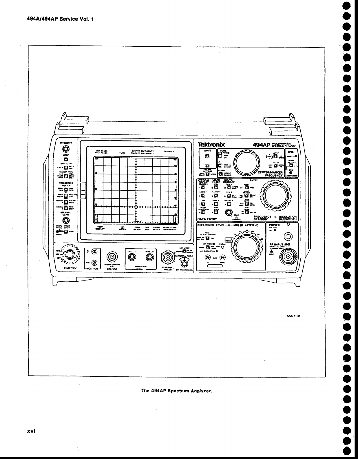
o
a
o
t
a
t
t
I
a
o
o
I
o
t
o
a
o
t
o
i
a
o
o
o
o
o
I
o
o
I
o
I
I
o
I
o
I
o
a
o
a
o
o
o
GENERAL
INFORMATION
Product Description
The 494A and the 494Ap (programmabte)
instru_
ments
are high performance,
compict, portable
spec-
trum analyzers.
Microcomputer
control
of most func-
tions simplifies
and
enhances
operation.
The
analyzers
feature:
. single
and
delta
marker
modes
o synthesizer
freguency
accuracy
o precision
signal
counting
r precise
amplitude
measurement
o digitat
storage
disptay
o internal memory for front-panel settings and
displays
o help
and
diagnostic
crt messages
. keypad
entry
and
menu
selections
r ability
to ptot
the
disptay.
readout,
and graticule
o ability
to hold
g personalized
macros
in memory
o 10
Hz
to 3 MHz
resolution
o multiband
sweep
capability
, The
frequency
range
is 10kHz to 21
GHz with the
internal
mixer,
extending
up to 925
GHz with ext€rnal
waveguide
mixers. Resolution
bandwidth
is 10
Hz to
3 MHz. Digital storage provides
flicker-free
displays
plus functions
to compare
and subtract
displays,
anO
save
maximum
values. In addition,
up
to nine
separate
displays
with their readouts
can be stored in battery-
powered
non-volatile
memory,
then later recalled
for
additional
analysis
and comparison.
Up to ten
different
front-panel
control
setups
can
also
be stored
for future
recall.
The
signal
counting
f€ature
allows
the spectrum
analyzer-to
selectively
count
a particular
signal out of
several
that may
be present
at its
input.
Select center frequency
either by the front-panel
tuning knob
or by the Data
Entry
keypad. When
using
the keypad,
it is not necessary
to alter the Span/Dii
setting
regardless
of the frequency
selected. oiher
parameters,
such as vertical display and reference
level,
are
also
keypad
selectable.
I
o
o
t
I
I
o
I
I
a
o
I
o
o
o
a
o
o
I
o
o
a
o
o
o
o
t
o
I
o
a
a
t
a
I
o
o
I
a
o
o
o
o
o
Sedon 1 - 4g4[l494Ap Servlce,
Vol. 1
Marker functions provide direct readout of fre-
quency
and
amplitude
at any
point
along
any
displayed
trace. Relative
(delta)
frequency
and
amplitude
informa-
tion-
betwe€n
any
two points
along
any
displayed
trace
is also available.
The
tuning knob
moves
ihe-markers,
and it can also
move
the display
with a stationary
fre-
quency
marker. lt is possible
to fix the marker
to a
position on the display
and use th€ knob
to move
both
the spectrum
and
the marker at the same
time. Refer
to using
the Markers
Feature
in section
6 of the
opera_
tors Manual.
The programmable
(p) version of the instrument
adds remote
control
capabilities
to the manual
instru_
ment features. The front-panel
controls (except
those
intended
exclusively
for local use, such ai lrufLruSlW1
can be remotely
operated
through
the
GplB port. Thia
allows
the spectrum
analyzer
to b€ used
with a variety
of systems
and
controllers.
Refer
to the programmers
Manual
for additional
information.
The programmable
instrument also adds the
macroinstructions
(macros)
feature. The,nstrument
memory
has
8K bytes
set aside
for the construction
of
made-to-order
macros.
The macro
menu
can
hold
the
titles of eight
macros
for easy access. Specific
macro
information
is located
in
the
programmers
Manuat.
Conformance to fndustry Standards
This spectrum
analyzer
complies
with
the following
Industry Safety Standards
and Regulatory
Require-
ments:
Safety
csA - Electrlcal
Bulletin
FM
- Electricat
Utitization
Standard
Ctass 3g20
ANSI C39.5
- Safety Requirements
for Etectrical
and Electronic
Measuring
and Controlling Instru-
mentation.
IEC
348
(2nd
edlton) - Safety
Requirements
for
Electronic
Measuring
Apparatus,
Regulatory
VDE 0871 Class B Regutations
for RFI
Suppression of High Frequency
Apparatus and
Installations.
Product Service
To assure adequate product service and mainte-
nance for our instruments,
Tektronix
has established
Field Offices and Service
Centers at strategic
points
1-1
Generaf
Infornation - 4g4[l4g4Ap Service,
Vol. 1
throughout
the
United
StatEs
and
in countries
wherE our
products
are sold. Several
types of maintenance
or
repair agreements
are
available.
For example,
for a fixed
fee, a maintenance
agree-
ment program
provides
maintenance
and recalibration
on a regular
basis. Tektronix
will remind
you when
a
product
is due
for r€calibration
and
perform
the
service
within
a specifi€d
time.
. Tektronix emergency repair service provides
immediate
service when the instrument
is urgently
needed.
Contact your local Tektronix SeMce Center,
representativer
or sales
engineer
for details
regarding
product
service.
I nstrument Construction
Modular
construction
provides
ready
access
to the
major circuits. Circuit
boards
containing
sensitive
cir_
cuits are either mounted
on metal castings,
each of
which
provides
shielding
between
adjacent
modules,
or
they ars mounted
within
honeycomb-like
castings,
with
feedthrough
connectors
through
the compartment
wall.
All boards
and assemblies plug onto a common
inter-
connect
board. Most adjustm€nls
and
test points
are
aecessible
while
the anstrument
is operational
and
with
the modules
or assemblies
secured
in
their
normal posi_
tion.
Extenders
are available
in an optional
Service
Kit
(see Maintenance
section
under Service
Fixtures
and
Tools for Maintenance).
Any module
or board
can be
removed
without
disturbing
the structural
or functional
integrity
of the other modules. The extenders
allow
most circuit board assemblies to function in an
extended
position
for service
or adjustment.
The
circuit
boards
mounted
on the metal
casting
can be removed
by removing
the securing
screws. All other circuit
boards (which should require minimal service)
are
accessible
by
removing
a cover plate
over
the assembly
or module.
Disassembly
of some
modules
may
require
special
tools and procedures.
These pro_
cedur€s are located in the Maintenance
section.
Circuits are isolated
in shielded
compartments
to
obtain
and maintain
th€ frequency
stability,
sensitivity,
and EMI characteristics.
While
shielding
hetps
ensuie
spurious-free
response,
the closeness
of the circuits
minimizes
losses
and interactions
with other
functions.
1-2
Compartments
are enclosed on both sides by metal
plat€s
and
interconn€ctions
between compartments
are
made by feedthrough
terminals rather
than cables. lf
the compartments
are
opened,
be sure
that
the shields
and
covers
are
properly
reinstalled
before
operating.
Installation and Preparation for Use
The Installation
section of the manual provides
unpacking information
and the procedures
to prepare
the instrum€nt
for use. lt also includes
repackaging
information.
Changing
Power lnput Range
The procedure
for changing
the input
voltage range
is described in the Installation section.
Details on how
to change
the line
fuse
are
also
given.
The
power
cord
that is supplied with
the instrument
and
the
instrument power
voltage
requirements
depend
on the available pow€r
source (see
Specification
sec-
tion). Power
cord options are
described in the
Options
section.
Replacing
Fuses
Refer
to the Installation section
for line
fuse
replace-
ment and the Maintenance
section
for replacing
the
power
supply
fuses.
Selected
Components
Some components are selected,
matched, or pre-
conditioned
to meet Tektronix specifications.
These
components
are shown
in
the
parts
list
and may
carry
a
Tektronix Part Number under the Mfr. Part Number
column.
Selected
value
components are identified on
the
cir-
cuit
diagram
and
in
the parts
list as a 'SEL"
value.
The
component
d€scription
lists either
the nominal value or
a range of values. Selection
criteria
is included in the
Maintenance section. Selection procedures are
included
in the Adjustment
Procedure or Maintenance
sections of the manual
as needed.
Assembly and Circuit Numbering
Each assembly and subassembly are assigned
assembly
numbers. Generally, each component is
assigned
a circuit
number according
to its geographic
location
within an assembly.
The
Replaceable
Electrical
Parts list prefixes these circuit numbers with the
corresponding
assembly
and subassembly
numbers.
o
o
o
t
a
t
o
o
o
a
I
a
o
a
o
a
o
o
o
I
a
o
o
o
o
o
I
a
a
I
o
o
o
a
I
o
a
a
o
o
o
o
o
a
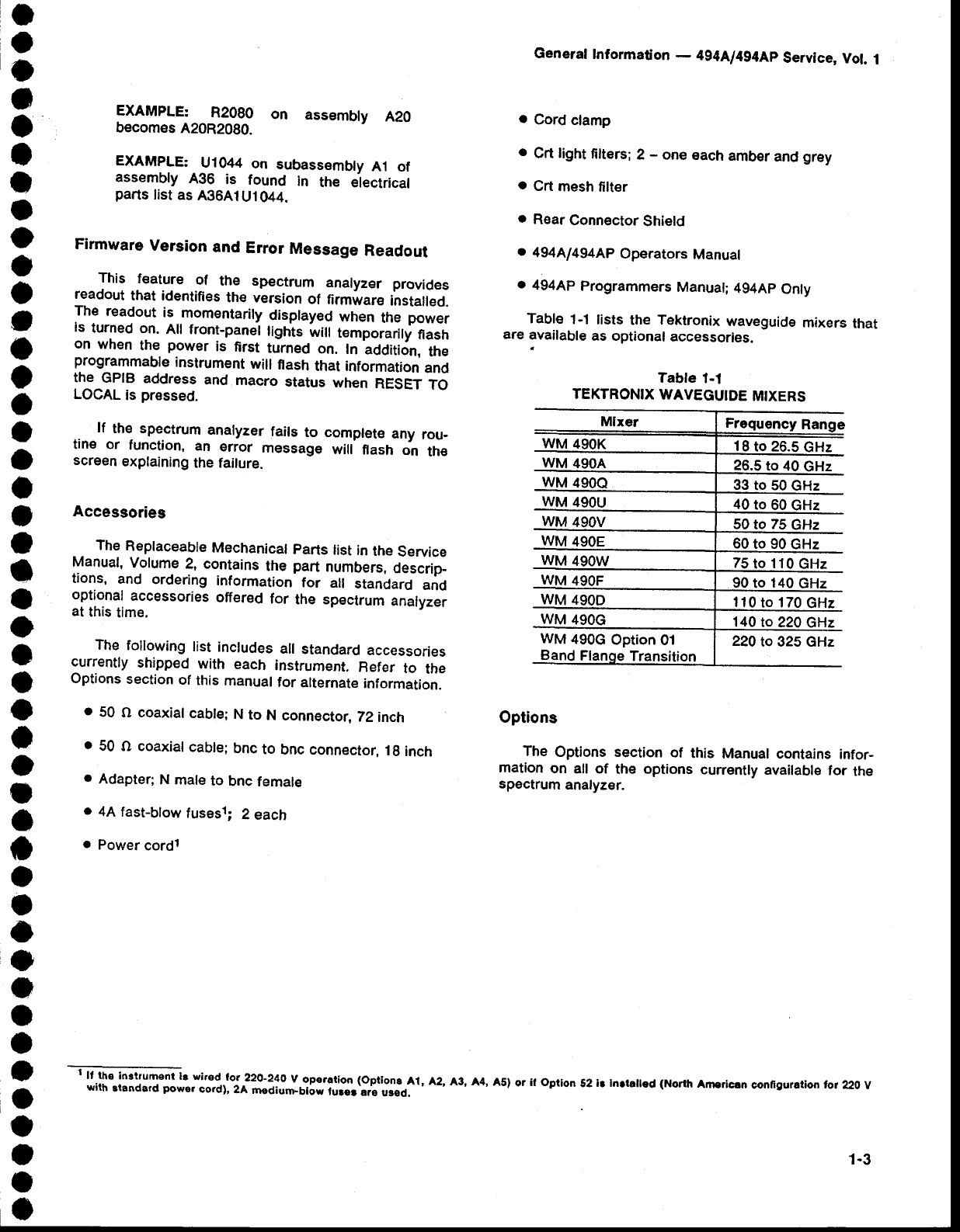
I
o
o
a
o
I
I
o
o
o
o
o
o
o
a
o
a
o
t
I
I
o
o
a
t
o
t
o
I
o
o
o
I
a
o
o
o
I
o
o
o
a
I
o
EXAMpLE: R2090 on assembly A2O
becomss
420R2090.
EXAMpLE: U1044
on subassemblv
Al of
assembly
A36 is found in the ejectrical
parts
tist
as
A3641U.t044.
Firmware Version and Eror Message Readout
This feature of the spectrum analyzer
provides
readout
that identifies
th€ version
of firmware
installed.
The readout
is momentarily
displayed
when
the power
is turned
on.
Ail front-panet
tights
ivitt
temporarily
flash
on when
the power
is first turned
on. In addition,
the
programmable
instrument
will flash
that information
and
the GplB address
and macro status
when
RESET
TO
LOCAL
is pressed.
lf the spectrum
analyzer
faits
to comptete
any rou-
tine or function,
an error message
will flash on th€
screen
explaining
the failure.
Accessories
The
Replaceable
Mechanical
parts
list
in
the
Service
Manual,
Volume
2, contains
the part numbers,
descrip-
tions, and ordering
information
for all standard
and
optional
accessories
offered
for the spectrum
analyzer
at
this
time.
The
following
list
includes
all
standard
accessories
currently
shipped
with each instrurnent.
Refer
to the
Options
section
of this
rnanual
for alternate
information.
. 50 O coaxial
cable;
N
to N connector,
72
inch
. 50 O coaxial
cable;
bnc
to bnc
connector,
1g
inch
. Adapter;
N male
to bnc
female
o 44 fast-blow
fusesl; 2 each
o Power
cordt
Generaf
Information
- 4g4Ll4g4Ap
Service,
Vol. 1
I cord clamp
. Crt light
filters;
2 - one each
arnber
and
grey
o Crt
mesh
filter
. R€ar
Connector
Shield
o 494A1494AP
Operators
Manual
. 494AP
Programrners
Manual;494Ap
Only
Table
1-1 lists the Tektronix
waveguide
mixers
that
are
available
as optional
accessories.
Tabte 1-l
TEKTRONIX
WAVEGUIDE
MIXERS
Mlxer
Options
The Options section
of this Manual
contains
infor-
mation
on all of the options
currently
available
for the
spectrum
analyzer.
It the insttument It wired lor 22o'24o v ope.ation (optiona.Al, A2, 43, 44, A5) or it opfion s2 lr Inrralled (North Arnerlc.n conliguration lot zloy
*ilh rtandsrd powe. cord), 2A medium_blow turerlr! used.
18
to
26.5
to
433 to 50
490U 40
to
WM 49OV
wM 490E
490W 110
GHz
490F GHz
wM4 | 10
to 170
GHz
ro
220
GHz
WM
490G
Option
01
1-3
a
o
o
I
o
I
a
O
o
o
o
t
o
t
o
o
o
o
I
I
a
I
o
a
o
o
I
a
I
t
o
o
I
o
o
I
o
a
I
o
o
o
a
o
I
o
a
I
o
o
o
t
o
o
o
J
o
o
o
o
I
a
t
a
I
a
o
o
o
o
o
o
I
o
I
o
I
a
o
C
I
o
o
o
o
I
I
o
Section
2 - 494A1494Ap
Service,
Vol.
1
SPECIFICATION
This section
includes
the eiectrical,
physical,
and
environmental
characteristics
of this insirument.
Any
instrument
specification
changes
due to options
ari
listed
in
the
Options
section
of
this
manual.
ELECTRICAL
CHARACTERI
STICS
- The following
tables
of electrical
characteristics
and
features
apply
to
the
spectrum
analyzer
after
a
3O_minute
warm up and after doing the front-panel
CAL adjust_
ments,
except
as noted.
The
performance
Requirement
column
defines
some
characteristics
in quantitative
terms
and
in limit
form.
The
Supplemental
lnformation
column
explains
performance
requirements
or provides
perfor-
mance
information.
Statements
in this column
are not
considered
to be guaranteed
performance
and are not
ordinarily
supported
by a performance
check
procedure.
P.rocedures
to verify
performance
requirements
are pro_
vided
in
the Performance
Check
portion
of
thrs
manual.
Table
2-1
FREOUENCY
RELATED
CHARACTERISTICS
The
instrument
performs
an
internal
calibration
check
each
tirne
power
is turned
on.
This
check
verifies
that
the
instrument
frequency
and amplitude performance
is as
specified.
An Instrument
Check
Out procedure,
which
requires
little
external
test equipment
or
technical
exper-
tise,
is provided
in Section
5 of the
Operators
Manual.
This procedure
will satisfy
most incoming
inspections
and
will
help familiarize
you
with
the
instrurnent
capabili-
ties.
Verification
of Tolerance Values
Perform
compliance
tests of specified
limits,
listed
in
the Performance
Requirernent
colurnn,
only after a 30_
minute
warm-up
time
(except
as
noted)
and
atter
a doing
the front-panel
CAL
procedure.
Use
measurement
instru-
ments
that
do
not
affect
the values
measured.
Measure_
ment
tolerance
of test equipment
should
be negligible
when
compared
to the specified
tolerance.
lf the
toler_
ance
is not negligible,
add the error
of the measuring
device
to
the
specified
tolerance.
Characteristic Performance
Requirement Supplemental
Intormation
Center
Frequency
Operating
Range
Internal
Mixer 10 kHz-21
GHz
Tuned by the CENTER/MARKER
FREQUENCY
control or the DATA
ENTRY
pushbuttons
External
Mixers
(optional) 10 kHz-325
GHz
Accuracy (after
front-panel
CAL
has
been
performed)
lnitial (start
of sweep)
Bands 1 & 5-12 with
SPANiDIV
>200 kHz, and
Bands 2-4 with SPAN/D|V
>100
kHz
(1st
LO unlocked)
*{2Oo/oD
+ (CF x REF)
+ 15N
kHz)
Where:
D : SPAN/D|V
or RESOLUTTON
BANDWIDTH, whichever is
greater
CF
- Center
Frequency
REF Reference Frequency
Error
N
: Harmonic
Number
Center Frequency Accuracy is
specified
by two characteristics:
. initial
accuracy (firmware
corrected)
o center
frequency
drift
during
the sweep
Refer to lF Frequency,
LO Range,
and Harmonic Number specification
later in this table for the N value
Allow a settling
time of one second
for each GHz change in CF within a
band.
In bands
4-'12,
divide
the CF
change
by N.
2-1
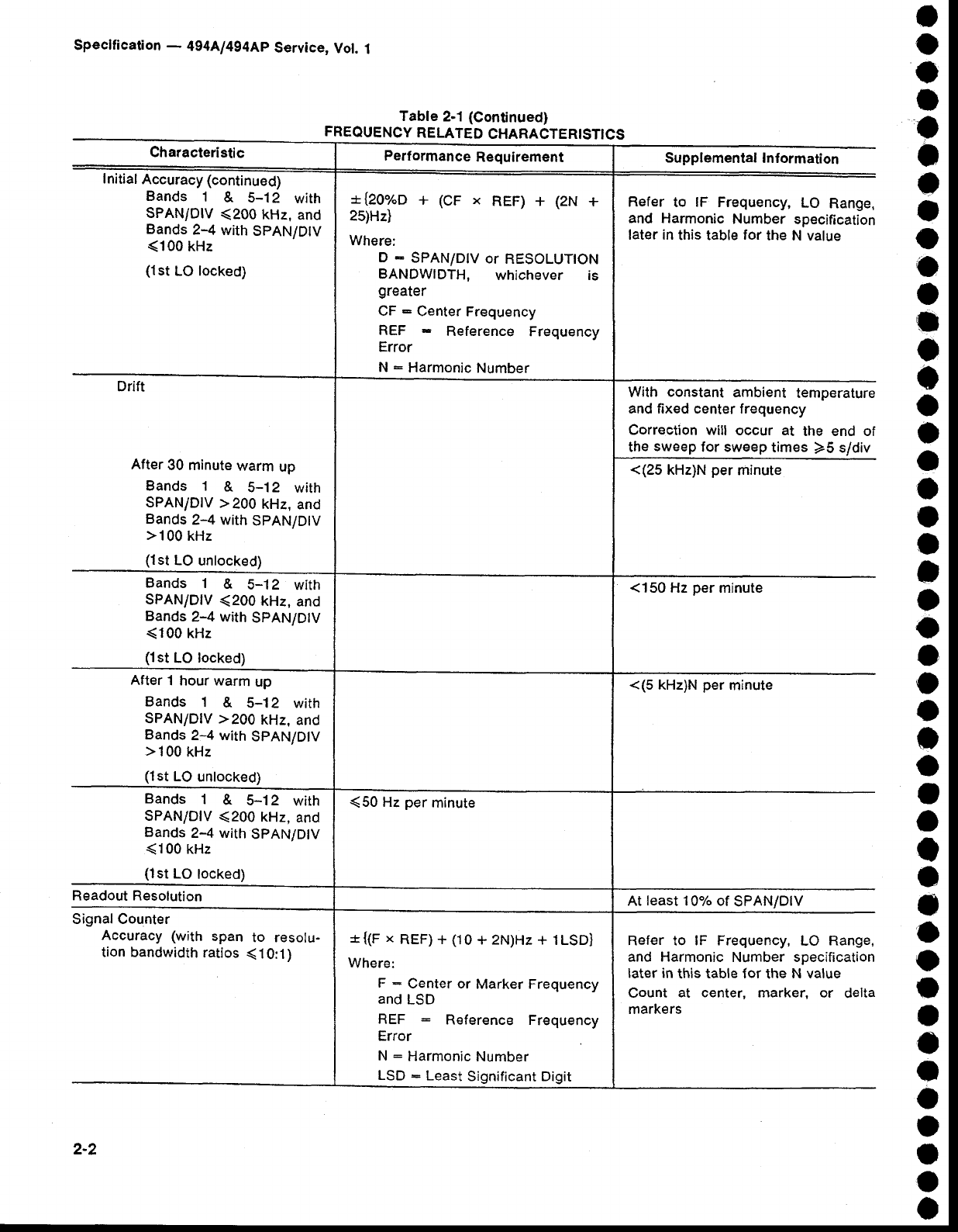
Table 2.1 (Continued)
Characteristic Perf
ormance
Requirement Supplemental Information
I nitial
Accuracy (continued)
Bands
1& 5-12 with
SPAN/DIV
(200 kHz,
and
Bands
2-4
with
SpAN/DlV
(100
kHz
(1st
LO locked)
t{20%D + (cF x REF) + (2N +
25)Hz)
Where:
D - SPAN/D|V
or RESOLUTTON
BANDWIDTH, whichever is
greater
CF
: Center
Frequency
REF Reference
Frequency
Error
N
: Harmonic
Number
Refer
to lF Frequency,
LO Range,
and Harmonic
Number
specification
later in
this table
for
the N value
Drift
After
30 minute
warm
up
Bands 1 & 5-12 with
SPANiDIV
>200 kHz,
and
Bands
2-4 with
SPAN/D|V
>100
kHz
(1st
LO
unlocked)
With constant
ambient
temperature
and fixed center frequency
Correction will occur at the end of
the
sweep
for sweep
times
>5 s/div
<(25
kHz)N
per
minute
Bands 1 & 5-12 with
SPAN/DIV
(200 kHz, and
Bands
2-4 with
SPAN/DtV
(100 kHz
(1st
LO locked)
<150
Hz
per
minute
After
t hour warm
up
Bands
1& 5-12 with
SPAN/DIV >200 kHz,
and
Bands
2-4 with
SpAN/DtV
>100
kHz
(1st
LO
unlocked)
<(5
kHz)N
per
minute
Bands
1& 5-12 with
SPAN/DIV
(200 kHz,
and
Bands
2-4 with
SPANiD|V
(100 kHz
(1st
LO
locked)
(50 Hz
per
minute
Readout
Resolution At
least
10% of
SPAN/DIV
Signal Counter
Accuracy (with
span
to resolu-
tion bandwidth
ratios
(10:1) *{(F x REF) + (10
+ 2N)Hz + lLSD}
Where:
F - Center or Marker Frequency
and
LSD
REF Reference Frequency
Error
N
- Harmonic
Number
LSD
: Least
Significant Digit
Refer to lF Frequency,
LO Range,
and Harmonic Number specification
later in this table for the N value
Count at center, marker, or delta
markers
a
o
a
I
'o
a
a
a
o
o
O
a
o
a
a
O
o
o
o
a
I
o
o
o
o
a
o
o
o
o
I
o
e
o
o
I
o
o
a
a
o
o
o
a
Specffication - 494A1494Ap
Service, Vol. 1
FREQUENCY
RELATED
CHARACTERISTICS
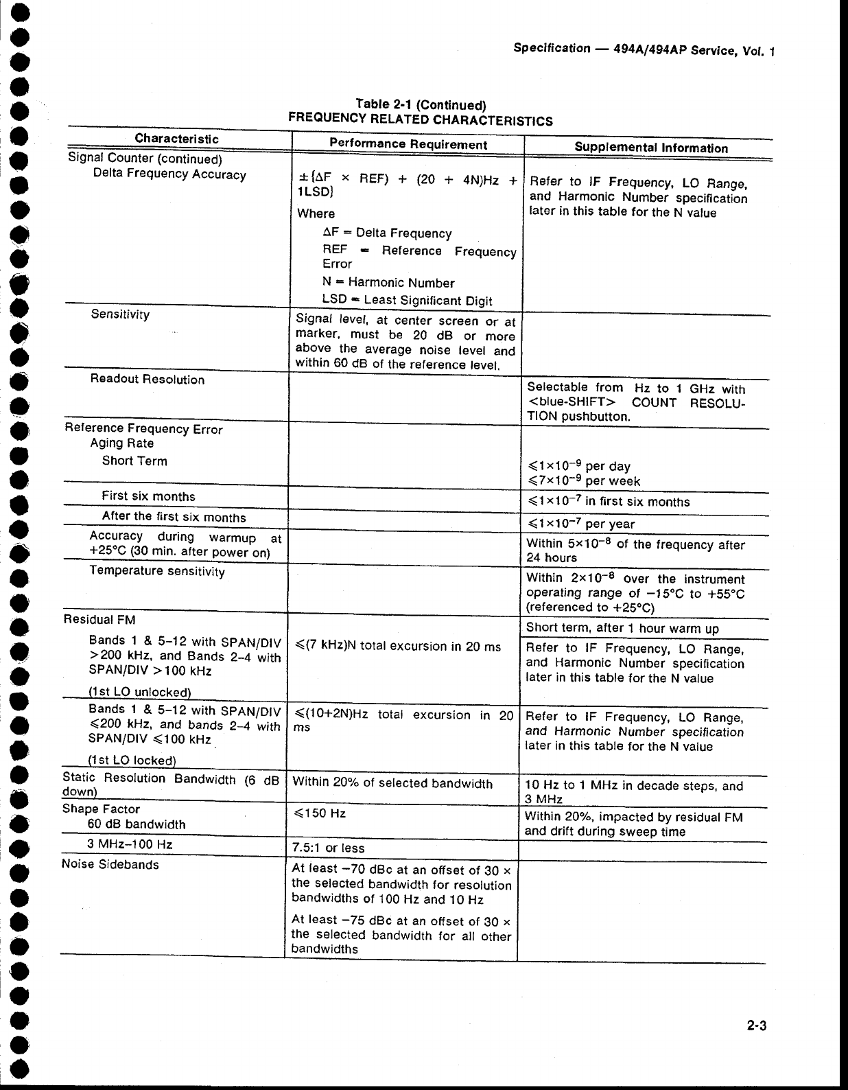
Specification
- 494Al4g4Ap
Service,
Vol.
1
- Tabte
2-1
(Continued)
FREOUENCY
RELATED
CHARACTERISTICS
tal
Inlormation
Characteristic
Signal
Counter
(continued)
Delta
Frequency
Accuracy
Sensitivity
Readout
Resolution
Ref
erence
Frequency
Error
Aging
Rate
Short
Term
First
six
months
After
the first
six months
Temperature
sensitivity
Residual
FM
1st
LO lock
Refer
to lF Frequency,
LO Range,
and Harmonic
Number
specification
later
in
this
table
for
the N vatue
(1x19-s
per
day
(7x10-e
per
week
Selectable
from Hz to 1 GHz
with
<blue-SHIFT> COUNT RESOLU-
TION
pushbutton.
Accuracy during warmup at
+25oC
(30
qlin.
after power
on)
(1x10⁻⁷ in
first
six
months
(1x.t0-z
per year
within 5x10⁻⁸ of the frequency
after
24 hours
Within
2x10⁻⁸ over the instrument
operating
range
ol -1 SoC
to +55"C
(referenced
to +25"C)
Short
terrn,
after
t hour warm
up
Refer
to lF Frequency,
LO Range,
and Harmonic
Number
specification
later
in
this table
for
the
N value
Refer to lF Frequency,
LO Range,
and Harmonic Number specification
later
in
this table
for the N value
10
Hz
to 1 MHz in
decade steps,
and
MHz
Within 20"h, impacted by residual
FM
and
drift during sweep
time
Bands
1 & 5-12
with
SpAN/D|V
>
200
kHz,
and
Bands
2-4 with
SPAN/DIV
>100
kHz
Bands
1 & 5-12 with
SpAN/DIV
(200 kHz, and bands 2-4 with
SPANID|V
(100 kHz
Static Resolution
Bandwidth (6 dB
down)
Shape
Factor
60 dB bandwidth
3
MHz-100
Hz
Noise
Sidebands
+tAF.
x BEF)
+ (20
+ 4N)Hz
+
1 LSD]
Where
AF: Delta
Frequency
REF Reference
Frequency
Error
N
: Harmonic
Number
!9D - Least
Significant
Digit
Signal
level,
at center
screen
or at
marker, must be 2A dB or rnore
above the average
noise level and
within
60
dB
of
the
reference
level.
((7 kHz)N
total excursion
in
20
ms
{(10+2N)Hz
total excursion
in 20
rns
Within
20/" ot selected
bandwidth
(150 Hz
7.5:1
or less
At least
-70 dBc at an offset
of 30 x
the selected
bandwidth
for resolution
bandwidths
of 100
Hz and 1O
Hz
At least
-75 dBc at an offset
of 30 x
the selected
bandwidth
for all other
bandwidths
2-3
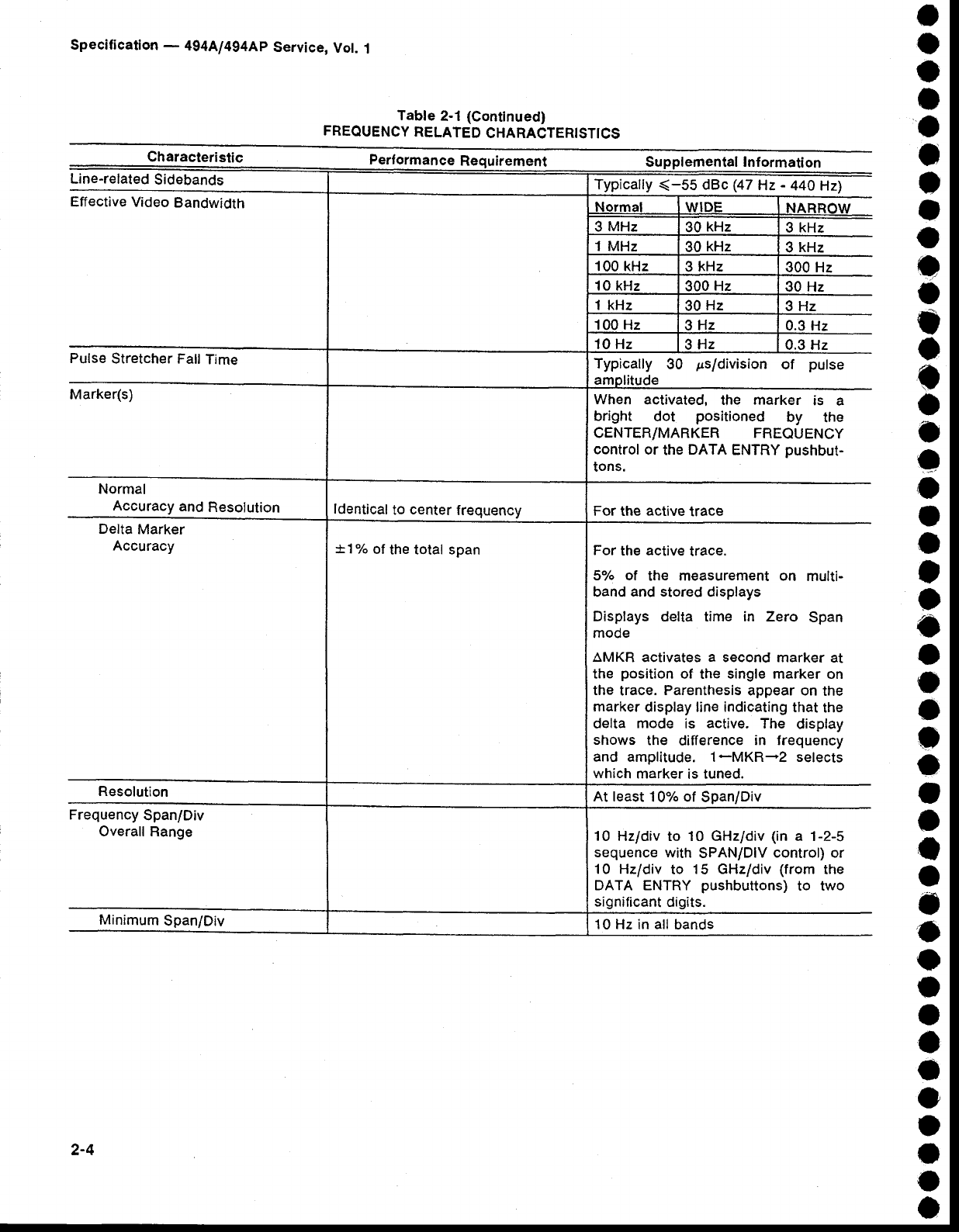
Specilication - 494A/494Ap Service, Vot. 1
Table
2-l (Continued)
FREQUENCY
RELATED
CHARACTERTSTICS
Characteristic Performance uirement Supplemental Inf ormation
cally (-55 dBc (47 Hz - 44A
Hz)
3
kHz
300 Hz
30 Hz
3Hz
0.3 Hz
Typically30 psldivision
of pulse
tude
When activated, the marker is a
bright dot positioned by the
CENTER/MARKER FREQUENCY
control or the DATA ENTRY
pushbut-
tons.
For the active
trace
For the active trace.
5/" at the measurernent on multi-
band and stored displays
Displays delta time in Zero Span
mooe
AMKR activates
a second marker at
the position
of the single
marker on
the trace.
Parenthesis
appear on the
marker
display
line indicating
that
the
delta mode is active. The display
shows the difference in frequency
and amplitude. 1-MKR-2 selects
which
marker
is tuned.
At least
10/ ot
Span/Div
10
Hzldiv to 10
GHz/div
(in
a 1-2-5
sequence with
SPAN/DIV
control) or
10 Hzldiv
to 15 GHz/div
(from
the
DATA ENTRY
pushbuttons)
to two
significant
digits.
10
Hz
in all
bands
Line-related
Sidebands
Effective Video
Bandwidth
Pulse
Stretcher Fall
Time
Marker(s)
Normal
Accuracy
and
Resolution
Delta
Marker
Accuracy
Resolution
Frequency
Span/Div
Overall Range
Minimum
Span/Div
kHz
ldentical
to
center
frequency
t1o/o
of the
tolal span
2-4
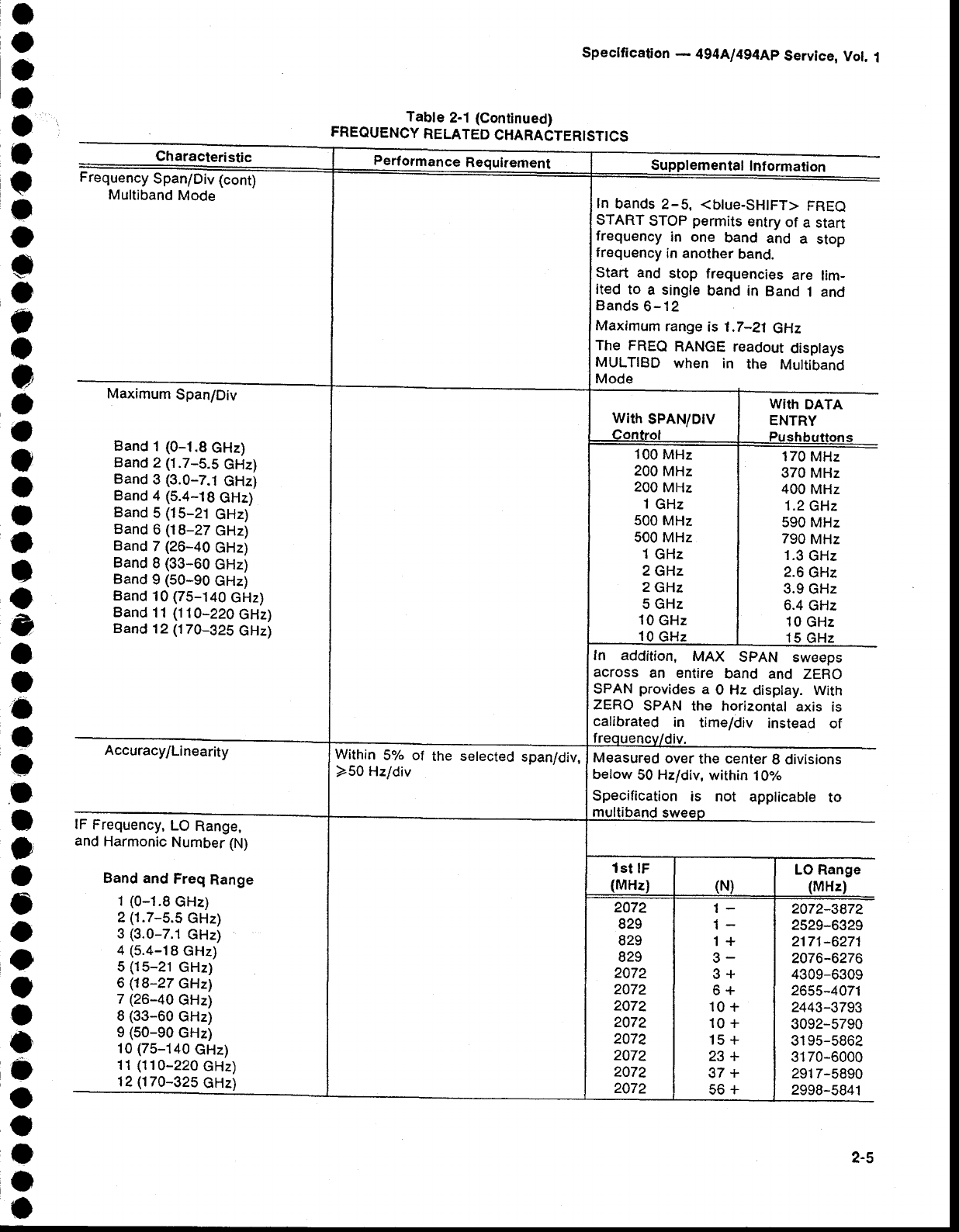
o
o
O
a
o
o
a
t
o
o
t
o
o
o
o
o
e
o
I
o
I
o
?
O
o
o
e
o
o
I
o
o
o
o
o
o
o
o
a
o
o
a
o
o
Characteristic
Frequency
Span/Div
(cont)
Multiband
Mode
Maximum
Span/Div
Band
1
(0-1.8
GHz)
Band
2
(1.7-5.5
GHz)
Band
3 (3.0-7.1
GHz)
Band
4 (5.4-18
GHz)
Band
5
(15-21
GHz)
Band
6
(18-27
GHz)
Band
7
(26-40
GHz)
Band
8
(33-60
GHz)
Band
9
(50-90
GHz)
Band
10
(75-140
GHz)
Band
11
(110*220
GHz)
Band
12 (170-325
GHz)
Specification
- 494A1494Ap
Service,
Vol.
1
Tabte
2-1
(Continued)
FREOUENCY
RELATED
CHARACTERISTICS
Supplemental
Intormation
In
bands
2-5, <btue-SHtFT>
FREQ
START
STOP
permits
entry
of a start
frequency
in one band and a stop
frequency
in another
band.
Start and stop frequencies
are lim-
ited
to a single
band in Band
1 and
Bands
6-12
Maximum
range
is
1.7-21
GHz
The FREQ
RANGE
readout
displays
MULTIBD
when in the Muttiband
Mode
With DATA
ENTRY
170
MHz
370
MHz
400
MHz
1.2GHz
590
MHz
790
MHz
1.3
GHz
2.6
GHz
3.9
GHz
6.4
GHz
10
GHz
ln addition, MAX SPAN sweeps
across an entire band and ZERO
SPAN provides
a 0 Hz display. With
ZERO SPAN the horizontal
axis is
calibrated in time/div instead of
f
Measured
over
the center
8 divisions
below
50 Hzldiv,
within
10%
Specification
as not applicable
to
iband
Accuracy/Linearity
lF
Frequency,
LO
Range,
and
Harmonic
Number
(N)
Band
and
Freq
Range
1
(0-1.8
GHz)
2
(1.7-5.5
GHz)
3
(3.0-7.1
GHz)
4
(5.4-18
GHz)
5
(15-21
GHz)
6 (18-27
GHzl
7 (26-40
GHz)
I (33-60
GHz)
9
(50-90
GHz)
10
(75-140
GHz)
11
(110-220
GHz)
12
(170-325
GHz)
LO Range
(MHz)
2072-3872
2529-6329
2't71-6271
2476-6276
4309-6309
2655-4071
2443-3793
3092-5790
31
95-5862
31
70-6000
291 7-s890
2998-5841
with SPAN/DtV
100
MHz
200
MHz
200
MHz
'l GHz
500
MHz
500 MHz
1
GHz
2GHz
2
GHz
5 GHz
10
GHz
10
GHz
Within 5% of the selected
span/div,
750 Hzldiv
2072
829
829
829
2072
2072
2072
2072
2072
2072
2072
2072
1-
t-
1+
3-
3+
6+
10+
10+
15+
23+
37+
56+
2-5
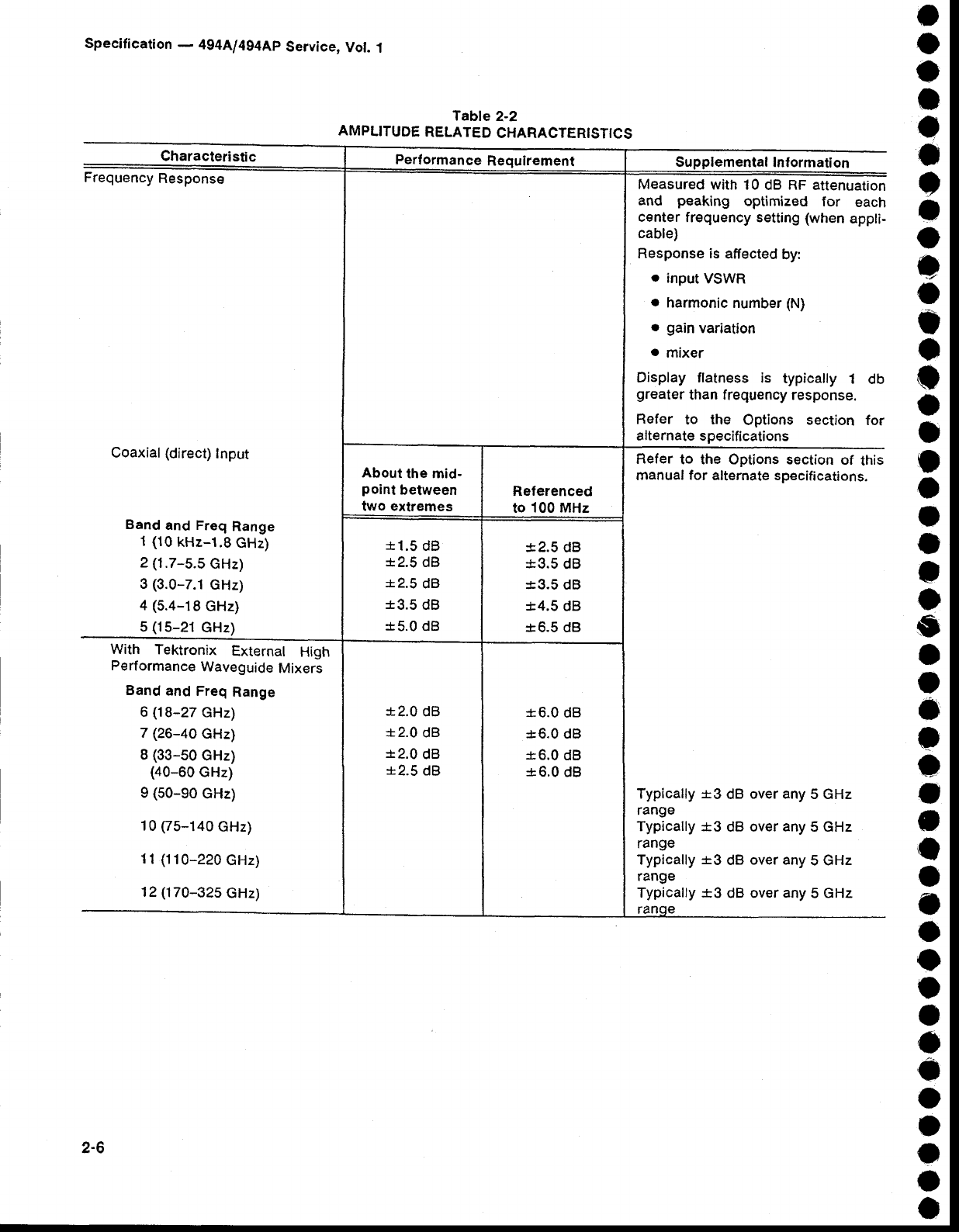
Characteristic Performance
Requirement Supplemental
Inf ormation
requency
Response
Coaxial
(direct)
Input
Band
and Freq
Range
1
(10
kHz-l.8 GHz)
2 (1.7-5.5
GHz)
3 (3.0-7.1
GHz)
4 (5.a-18
GHz)
5
(15-21
GHz)
Measured
with 10
dB
RF
attenuation
and peaking optimized for each
center
frequency setting (when
appli-
cable)
Response is affected
by:
o input
VSWR
r harmonic
number
(N)
o gain
variation
. mixer
Display flatness
is typically
1 db
greater
than frequency response.
Refer to the Options section for
alternate specifications
About
the mid-
point
between
two extremes Referenced
to 100 MHz
Refer to the Options section
of this
rnanual
for alternate specifications.
Typically
:h3
dB
over any
5 GHz
range
Typically +3 dB
over any
5 GHz
range
Typically
13 dB
over any
5 GHz
range
Typically *3 dB over
any
5 GHz
r1.5
dB
*2.5
dB
12.5
dB
a3.5
dB
f 5.0
dB
i2.5 dB
*3.5
dB
:t3.5
dB
r4.5 dB
:86.5
dB
With Tektronix External High
Performance
Waveguide
Mixers
Band
and Freq Range
6
(18-27
GHz)
7 (26-a0 GHz)
8
(33-s0
GHz)
(40-60
GHz)
9 (50-90 GHz)
10 (75-140
GHz)
11 (110-220
GHz)
12
(170-325
GHz)
*2.0
dB
*2.0
dB
+2.0
dB
*2.5
dB
f 6.0 dB
*6.0 dB
*6.0 dB
*6.0 dB
a
o
o
o
a
e
a
o
o
e
o
t
o
o
o
I
t
a
o
o
a
o
s
a
o
o
o
o
o
a
o
o
?
o
o
o
a
o
e.
a
I
o
o
a
Specification - 494A,1494Ap
Service, Vol. 1
Table 2-2
AMPLITUDE
RELATED
CHARACTERISTICS
2-6
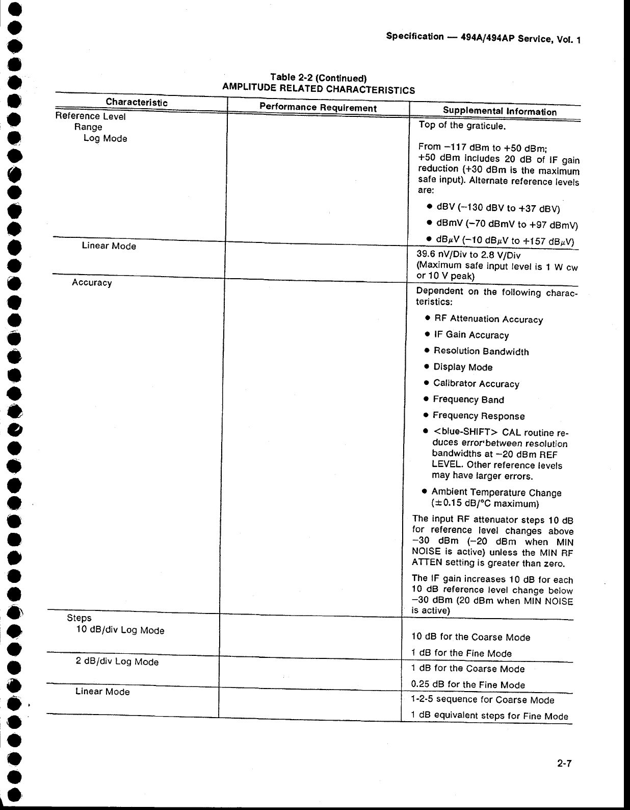
Characteristic
Specification
_ 494A1494Ap
Service,
Vot.
1
AMPLITUDE
RELATED
CHARAiTERISTICS
tal Informalion
Top
of the
graticule.
From
-117
dBm
to +50
dBm;
+50 dBm
inctudes
20 dB of tF gain
reduction
(+30
dBm is the maximum
safe
input).
Alternate
reference
levels
arei
. dBV
(-130
dBV
to +97
dBV)
o dBrnv
(-70 dBmV
to +97
dBmV)
o dBpV (-10 dBpV
to +157 dBpV)
39.6
nV/Div
to 2.8
v/Div
(Maximum
safe
input
level
is .t
W
cw
orl0Vpeak)
Dependent
on the foltowing
charac-
teristics:
. RF
Attenuation
Accuracy
o lF
Gain
Accuracy
r Resolution
Bandwidth
. Display
Mode
o Calibrator
Accuracy
. Frequency
Band
o Frequency
Response
o <blue-SHIFT>
CAL
routine
re_
duces error,between
resolution
bandwidths
at
-20 dBm
REF
LEVEL.
Other
reference
levels
may
have
larger
errors.
o Ambient
Temperature
Change
(+0.15
dB/"C
maximum)
The
input
RF
attenuator
steps
10
dB
for reference
level changes
above
-30 dBm (-20 dBm when MtN
NOISE
is active)
unless
the MIN
RF
ATTEN
setting
is greater
than zero.
The
lF
gain
increases
10
dB for each
10
dB reference
level
change
below
-30 dBm
(20
dBm when
MtN
NOISE
is
active)
'1
0 dB for the
Coarse
Mode
1 dB for the Fine
Mode
1 dB for the
Coarse
Mode
0.25
dB for the Fine
Mode
1-2-5
sequence
for Coarse
Mode
1
dB equivalent
steps
for Fine
Mode
Reference
Level
Range
Log Mode
Linear
Mode
Accuracy
Steps
10
dB/div
Log
Mode
2 dBldiv
Log Mode
Linear
Mode
2-7
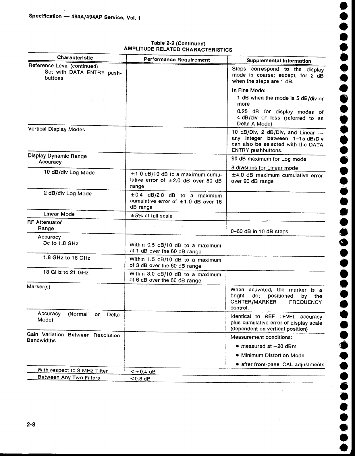
Specification - 494A!494Ap
Service, Vol. 1
Characteristic
Reference
Level (continued)
SEt With
DATA ENTRY
buttons
Vertical
Display
Modes
Display
Dynamic
Range
Accuracy
10
dB/div Log Mode
2 dBldiv Log Mode
Linear
Mode
RF
Attenuatol
Range
Accuracy
Dc
to 1.8
GHz
1.8
GHz to
'l8
GHz
18
GHz
to 2'l
GHz
Marker(s)
Accuracy
Mode) (Normal or Delta
Gain Variation
Bandwidths Between Resolution
3 MHz Fi
Table 2-2 (Continued)
AMPLITUDE
RELATED
CHARACTERISTICS
Supplemental
Information
push- Steps correspond to the disptay
mode in coarse; except, tor 2 dB
when
the steps are
1
dB.
In Fine
Mode:
1 dB when
the
mode
is
5 dB/div
or
more
0.25 dB for display modes of
4 dB/div or less (referred
to as
Delta
A Mode)
10 dB/Div, 2 dB/Div, and Linear
-
any integer between 1-1
5 dBlDiv
can also be selected with the DATA
ENTRY
pushbuttons.
90
dB maximum
for Log
mode
slons
for Linear
mode
+4.0 dB maximum
cumulative
error
over
90
dB range
0-60
dB in
10 dB
steps
When activated, the marker is a
bright dot positioned by the
CENTER/MARKER FREQUENCY
control,
ldentical
to REF LEVEL accuracy
plus
cumulative
error
of
display scale
(dependent
on
vertical
position)
Measurement
conditions:
o measured
at
-20 dBm
o Minimum
Distortion
Mode
o after
front-panel
CAL
adjustments
2-8
*1.0 dB/l0
dB to a
maximum cumu-
lative
error
of *2.0 dB over
B0 dB
range
40,4 dBP.A dB to a maximum
cumulative
error
o,f
+1.0 dB over 16
dB range
t5o/" ot full scale
Within
0.5 dB/10
dB to a maximum
of 1 dB over
the
60 dB range
Within
1.5
dB/10
dB to a maximum
of 3 dB over
the
60 dB range
Within
3.0 dB/10
dB to a maximum
of
6
dB over
the
60
dB range
<
i0.4 dB
Two Filters
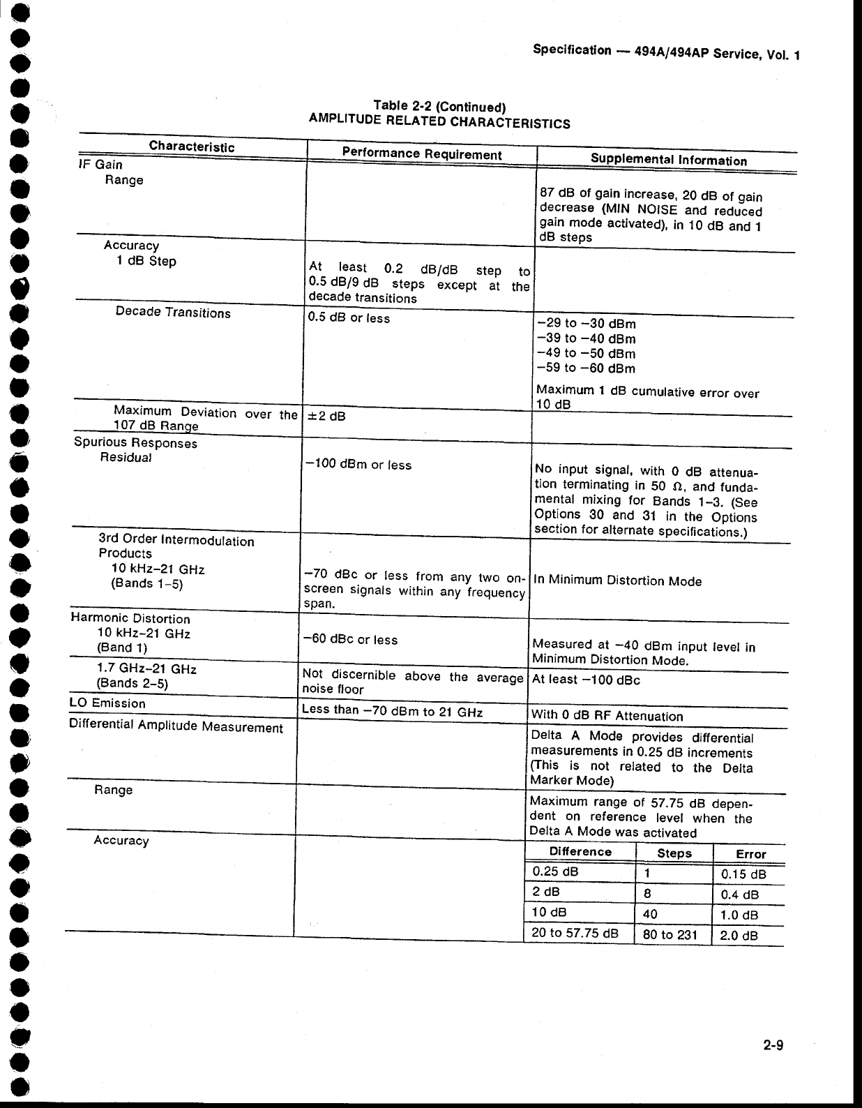
o
o
o
I
o
o
o
o
o
o
o
c
I
o
o
o
o
o
a
o
I
o
o
)
o
o
o
o
I
o
?
o
a
o
O
o
o
I
o
o
a
o
I
o
Specification
_ 494A1494Ap
Service,
Vot.
1
Tabte
2-2
(Continued)
AMPLITUDE
RELATED
CHARAiTERISTICS
Characteristic
lF Gain
Range
Accuracy
'l dB Step
..--
Decade
Transitions
Maximum Deviation
107
dB Range
Spurious
Responses
Residual
the
3rd
Order
Intermodulation
Products
10
kHz-21
GHz
(Bands
1-5)
Harmonic
Distortion
10
kHz-21
GHz
(Band't)
't.7
GHz-21
GHz
(Bands
2-5)
LO
Emission
-
Differential
AmplitudeMeasurement
Range
Performancq
Requirement emehlrl lnfarnari
87 dB of gain increase,
20 dB of gain
decrease
(MlN NOISE and reduled
gain mode activated),
in 10 dB and j
dB steps
lt_ ielst 0.2 dB/dB step to
0.5
dB/g
dB steps except at the
decade
transitions
-29 to
-30 dBm
-39 to
-40 dBm
-49 to
-50 dBm
-59 to
-60 dBm
Maximum
1 dB
cumulative
error
over
10 dB
0.5
dB or
less
*2 dB
No input
signal,
with
0 dB attenua_
tion
terminating
in 50 O, and
funda_
mental
mixing
for Bands
1_3. (See
Options
30 anO
gl in the Options
section
for
alternate
specifications.)
In
Minimum
Distortion
Mode
-100
dBm
or
less
-70 dBc or less from any two on_
screen
signals
within any frequency
span.
-60 dBc
or
less Measured
at -40 dBm input level
in
Minimum
Distortion
Mode.
Not discernible
above the average
noise
floor At least
-100
dBc
Less
than
-70 dBm to 21
GHz With 0 dB RF Attenuarion
Delta A Mode provides
differential
measurements
in
0.25
dB increments
(This is not related to the Delta
Marker
Mode)
Maximum
range
of SZ.7S
dB depen-
dent on reference level when the
Deita
A Mode
was activated
Ditference Steps Error
0.25 dB 10.15 dB
2dB I0.4 dB
10
dB 40 1.0
dB
2.0
dB
20
to 57.75
dB 80 to 231
2-9
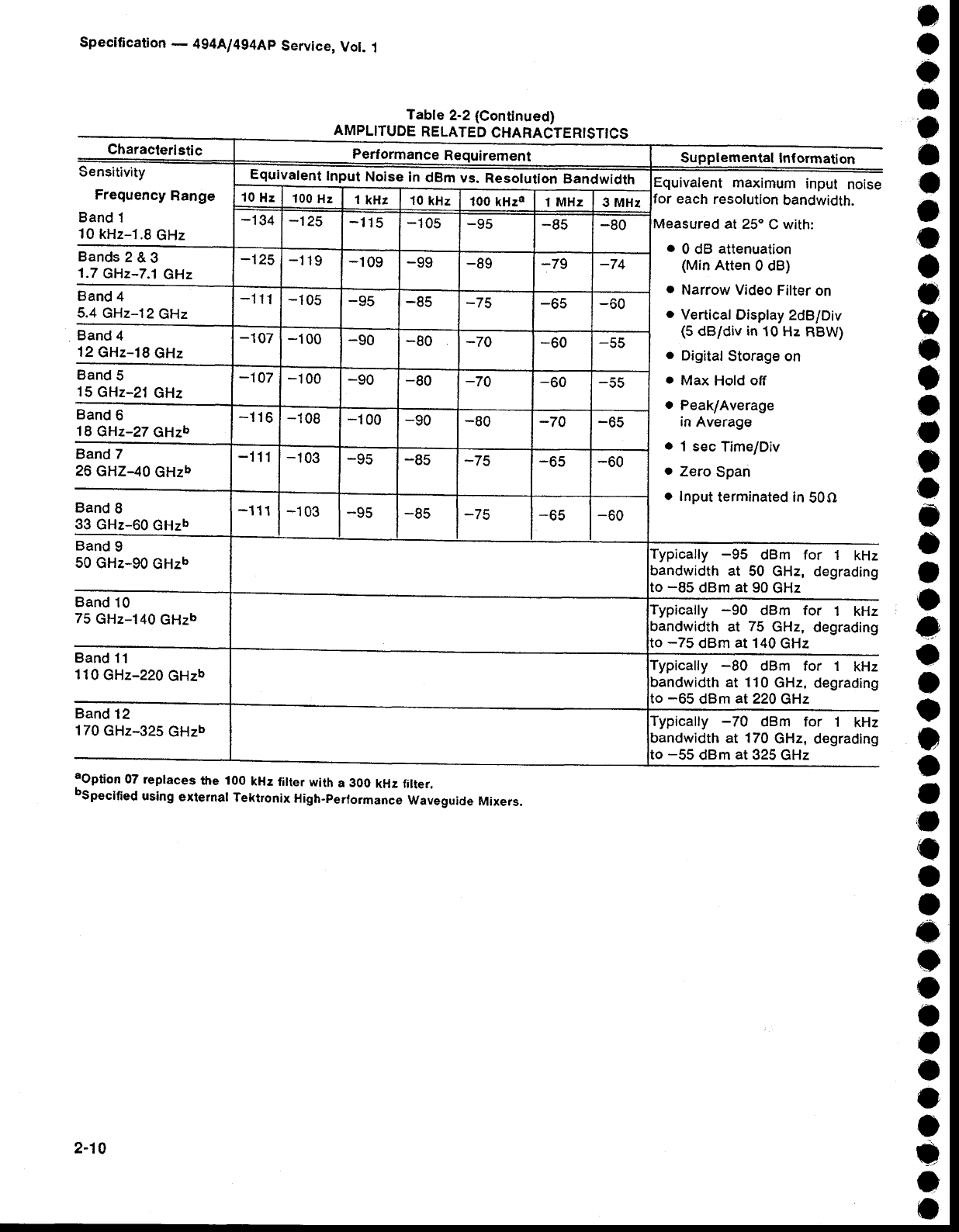
Table
2-2 (Continued)
Characteristic Perf
grmance
Requirement Supplemental Intormation
Sensitivity
Frequency
Range
Band
1
10
kHz-'t.8
GHz
Equivalent
Input
Noise
in dBm
vs. Resolution
Bandwidth quivalent
maximum
input
noise
rr
each
resolution
bandwidth.
leasured
at
25"
C with:
. 0 dB attenuation
(Min
Atten
0 dB)
o Narrow Video
Filter
on
. Vertical Display
2dBlDiv
(5
dBidiv
in
10 Hz
RBW)
o Digital
Storage on
o Max
Hold
off
o Peak/Average
in
Average
o 1
sec Time/Div
o Zero
Span
o lnput
terminated in
50O
10
Hz 100
Hz 1
kHz 10
kHz 100
kHza 1 MHz 3 MHz
-134 -125 -115 -10s -v5 -85 -80
Bands
2
&
3
1.7
GHz-7.1
GHz -125 -'t
19 -1
09 -99 -89 -79 -74
Band
4
5.4
GHz-12
GHz
-111 -105 -YC -85 - //b -65 -60
Band
4
12
GHz-'t8
GHz
-107 -100 -90 *80 -74 *60 -55
Band
5
15
GHz-21
GHz
-'a07 -1
00 -90 -80 -70 -60 -55
Band
6
18
GHz-27
GHzu
-116 -108 -100 -90 -80 -70 -oc
Band 7
26 GHZ-40
GHzb
-111 -103 -v5 -85 -75 -65 -60
Band
8
33
GHz-60
GHzb
-11
1-103 -qq -85 -{5 -65 -60
Band
9
50
GHz-90
GHzb pically -95 dBm for 1 kHz
ndwidth at 50 GHz, degrading
-85 dBm at 90
GHz
Band
10
75
GHz-l40
GHzb pically -90 dBm for 1 kHz
ndwidth at 75 GHz, degrading
-75 dBm at'140
GHz
Band 11
110
GHz-220
GHzb pically -80 dBm for 1 kHz
ndwidth
at 110
GHz,
degrading
-65 dBm at220GHz
Band
12
170
GHz-325
GHzb pically -70 dBm for 1 kHz
ndwidth
at 170
GHz, degrading
-55 dBm
at
325 GHz
e
o
o
I
o
t
a
)
o
o
o
t
o
I
o
I
o
o
c
o
I
o
o
a
t
o
o
O
o
o
e
o
t
o
c
o
o
a
o
o
o
o
)
o
Specification - 4g4[l4g4Ap Service,
Vol. 1
AMPLITUDE
RELATED
CHARACTERISTICS
aOption
07 replaces the 100 kHz fitter with a 300 kHz filter.
bspecified using externar rektronix High-performance
waveguide Mixers.
2-10
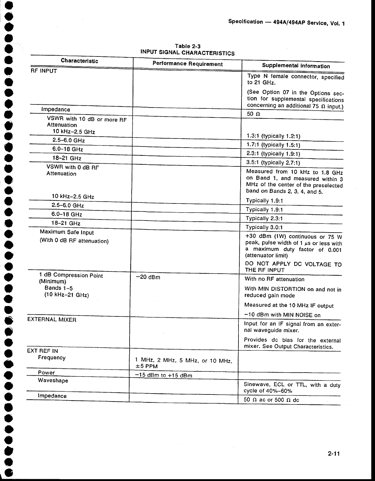
I
o
o
t
o
I
o
I
o
t
I
o
o
I
a
I
o
o
o
o
I
o
o
o
o
O
t
e
t
c
o
o
o
o
o
o
o
I
o
o
o
I
t
3
Characteristic
RF INPUT
lmpedance
VSWR
with
10
dB or more
RF
Attenuation
10
kHz-2.5
GHz
2.5-6.0
GHz
6.0-18
GHz
18-21
GHz
VSWR
with
0
dB
RF
Attenuation
10 kHz-2.5
GHz
2.5-6.0
GHz
6.0-18
GHz
18-21
GHz
Maximum
Safe Input
With 0 dB
RF attenuation)
1
dB
Compression
point
(Minimum)
Bands
1-5
(10
kHz-21
GHz)
EXTERNAL
MIXER
EXT
REF
IN
Frequency
Waveshape
Tabte
2-3
INPUT
SIGNAL
CHARACTERISTICS
Specification - 4g4Al494Ap
Service, Vol. 1
Supplemental
Inf
ormaton
Type N female
connector,
specifieO
to 21
GHz.
(See
Option
07 in the Options
sec-
tion for supplemental
specifications
concerning
an
additional
75
O input.)
50()
1.3:1 (typically
1.2:1)
1.7:1 (typically
1.5:1)
2.3:1 (typically
1.9:'t
)
3.5:1
(typically
2.7:1)
Measured from '1
0 kHz to 1.9 GHz
on Band 1, and measured
within 3
MHz of the center
of the preselected
band on
Bands
2,3,4, and
5.
Typically
1.9:1
Typically
1.9;'l
Typically
2.3:1
Typically
3.0:1
+30 dBm (1W) continuous
or 75 W
peak,
pulse
width
of 1
ps or less
with
a maximum duty factor of 0.001
(attenuator
limit)
DO NOT APPLY DC VOLTAGE TO
THE
RF INPUT
With
no RF attenuation
With
MIN DISTORTION
on and
not
in
reduced gain
mode
Measured
at the 10 MHz
lF output
-10 dBm with
MtN
NOTSE
on
Input for an lF signal
from an exter-
nal waveguide
mixer.
Provides dc bias for the external
mixer.
See
Output
Characteristics.
Sinewave, ECL or TTL,
cycle of 40%-60% with a duty
1 MHz,
2 MHz,
S MHz, or 10 MHz.
*5 PPM
-15 dBm
to +15
dBm
lmpedance 50Oacor500Odc
2-11
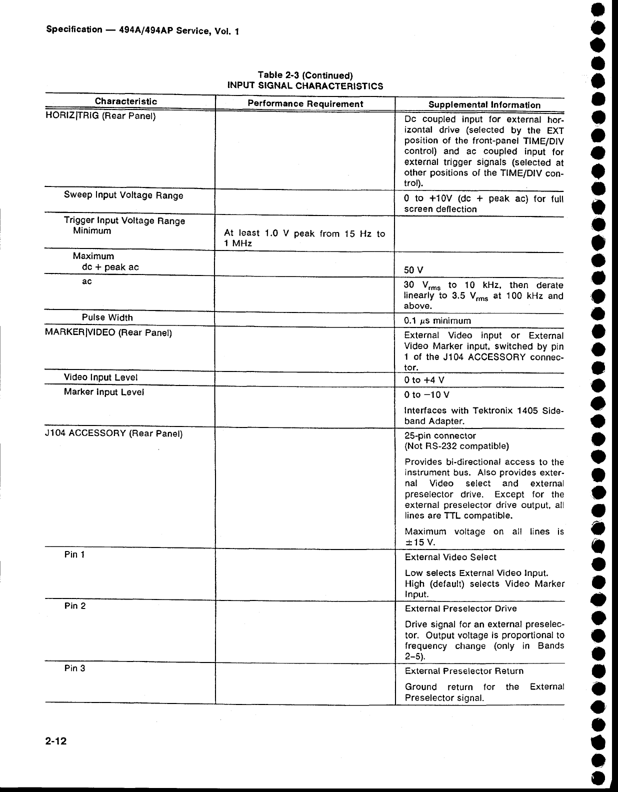
Specification - 494A1494Ap
Service, Vol. 1
Characteristic
HORIZITBIG
(Rear
Panel)
Sweep Input
Voltage
Range
Trigger
Input
Voltage
Range
Minimum
Maximum
dc
+ peak
ac
Pulse
Width
MARKERIVIDEO
(Rear
Panet)
Video
lnput
Level
Marker
Input
Level
J104 ACCESSORY (Rear
Panet)
Pin
1
Pin 2
Pin 3
Table 2-3 (Continued)
INPUT
SIGNAL
CHARACTERISTICS
Supplemental Inf
ormatlon
Dc coupled
input for external
hor-
izontal drive (selected
by the EXT
position
of the front-panel
TIME/DIV
control)
and ac coupled
input for
external
trigger
signals (selected
at
other
positions
of the
TIME/Dlv
con-
trol).
0 to +10V (dc * peak
ac) tor tutl
screen
deflection
50v
30 vrms
to 10 kHz,
linearly
to 3.5 Vr." at
above.
0.1
rs minimum
External
Video input or External
Video
Marker
inpul,
switched
by pin
1 0f the
J104 ACCESSORY connec-
tor.
0to*4V
0 to
-10 V
lnterfaces with Tektronix
1405 Side-
band
Adapter.
25-pin connector
(Not
R5-232
compatible)
Provides
bi-directional
access
to the
instrument
bus. Also
provides
exter-
nal Video select and external
preselector drive. Except for the
external
preselector
drive output, all
lines are TTL
compatible.
Maximum voltage on all lines is
+'l5 v.
External Video
Select
Low selects External
Video
lnput.
High (default)
selects Video Marker
Input.
External
Preselector
Drive
Drive
signal
for an
external
preselec-
tor. Output
voltage
is proportional
to
frequency change
(only in Bands
2-s\.
External Preselector Return
Ground return for the External
Preselector
siqnal.
then derate
1
00 kHz and
t
o
o
I
a
a
t
o
a
I
I
I
o
I
o
o
,o
o
o
o
a
o
e
o
o
I
t
o
a
o
a
o
o
o
o
o
a
C
o
o
o
a
t
o
At least
1.0 V peak
from 15 Hz to
1 MHz
2-12
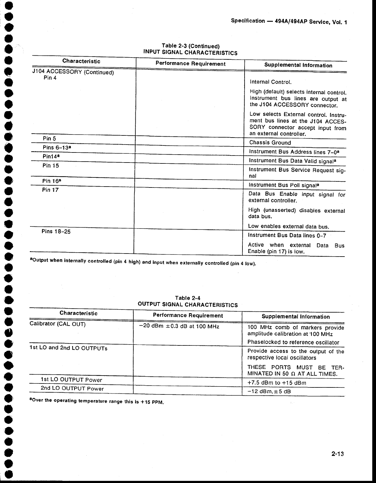
Characteristic
Speclfication
- 494Al4g4Ap
Service,
Vol.
1
Table
2-3
(Continued)
INPUT
SIGNAL
CHARACTERISTICS
Supplemental
Inf ormation
Internal
Control.
High (default)
selects
internal
control.
lnstrument
bus lines
are output
at
the
J104 ACCESSORy
connector.
Low selects
External
control.
lnstru-
ment
bus lines
at the
J104
AccES-
SORY
connector
accept
input from
an
external
controller.
Chassis
Ground
Instrument
Bus Address
lines
7-0a
Instrument
Bus
Data
Valid
signala
Instrument
Bus
Service
Request
sig-
nal
Instrument
Bus Poll
signala
Data Bus Enable input signal for
external
controller.
High (unasserted)
disables external
data
bus.
Low
enables
external
data
bus.
Instrument
Bus
Data
lines
0-7
Active when external Data Bus
Enable
(pin
17) is
low.
J1 04
ACCESSORy
(Continued)
Pin 4
Pin
5
Pins
6-13a
Pin14a
Pin
15
Pin
16a
Pin 17
Pins
18-25
soutput when internally controlled {pin 4 high) and input when externally controled (pin 4 low).
Table
2-4
OUTPUT
SIGNAL
CHARACTERISTICS
Characteristic Perf
ormance
Requirement Supplemental
Inlormation
ualrbrator
(cAL ouT) -20 dBm *0.3 dB
at
100
MHz 100 MHz comb of markers provide
amplitude
calibration
at-1
00 MHz
Phaselocked
to reference
oscillator
1st
LO and
2nd LO OUTpUTs Provide
access to the output of the
respective
local oscillators
THESE PORTS MUST BE TER-
MINATED
IN 50 O AT
ALL TIMES.
1st LO
OUTPUT
power +7.5
dBm
to
+15
dBm
2nd
LO OUTPUT
power -12
dBm.*5
dB
aover lhe operating temperature range this is +15 ppM.
2-13
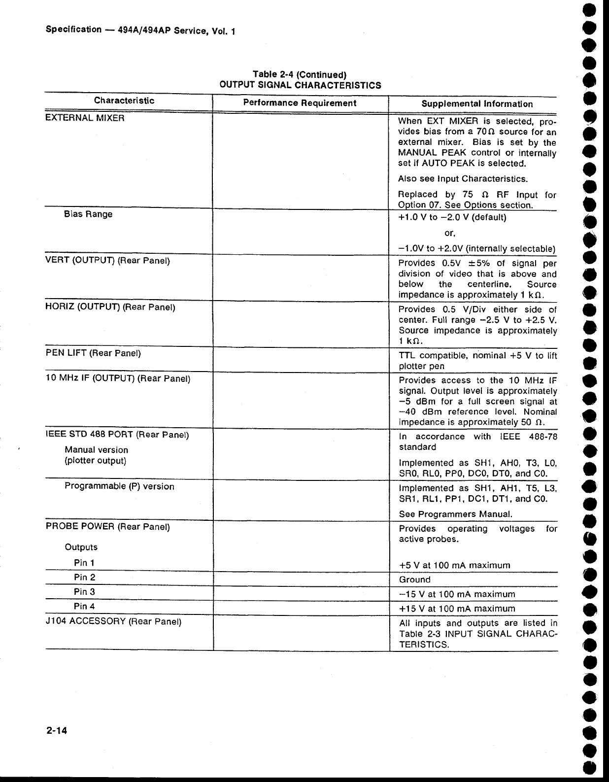
Specification
- 494At494Ap
Service,
Vol.
1
Characteristic
EXTERNAL
MIXER
Bias
Range
VERT (OUTPUT)
(Rear
Panet)
HORIZ
(OUTPUT)
(Rear
panet)
PEN LIFT
(Rear
Panel)
10 MHz lF (OUTPUT)
(Rear
Panet)
IEEE
STD
488
PORT (Rear
Panel)
Manual
version
(plotter
output)
Programmable
{P)
version
PROBE
POWER (Rear
Panet)
Outputs
Pin 1
Pin 2
Pin
3
Pin 4
J104 ACCESSORY
(Rear
Panet)
Table
2-4
(Continued)
OUTPUT
SIGNAL
CHARACTERISTICS
Supplemental
lnformation
When
EXT MIXER
is selected, pro-
vides
bias from
a 70f,) source
for an
external
mixer. Bias is set by the
MANUAL
PEAK
control
or internally
set if AUTO
PEAK
is
selected.
Also
see Input
Characteristics.
Replaced by 75 O RF Input for
ion
07. See Ootions
+1.0
V to
-2.0 V
(default)
or.
-1.0V
to
+2.0V
(internally
selectable)
Provides 0.5V t5% of signal per
division of video that is above and
below the centerline. Source
impedance
is approximately
1 kO.
Provides
0.5 V/Div either side ol
center. Full
range
-2.5 V to +2.5
V.
Source
impedance is approximately
1 ko.
TTL compatible,
nominal +5 V to lift
plotter pen
Provides
access to the 10 MHz lF
signal.
Output
level
is approximately
-5 dBm for a full screen signal at
-40 dBm reference level. Nominal
impedance
is approximately
50 O.
ln accordance with IEEE 488-78
standard
lmplemented as SHl, AHo, T3, L0,
SR0,
RL0, PP0,
DC0,
DT0, and
C0.
lmplemented as sH1, AH1,
T5, L3,
SR1,
RL1.
PP1,
DC1, DT1, and
C0.
See
Programmers Manual.
Provides operating voltages for
active probes.
+5 V at'1
00
mA maximum
Ground
-15 V at 100
mA
maximum
+'15
V
at
100 mA
maximum
All inputs and outputs
are listed in
Tab|e 2.3 INPUT SIGNAL
CHARAC.
TERISTICS.
o
o
o
I
I
I
t
o
o
o
o
I
o
o
O
o
o
I
l
t
I
o
o
o
o
o
I
o
I
t
o
o
o
o
o
t
o
I
o
o
o
a
o
f
2-14
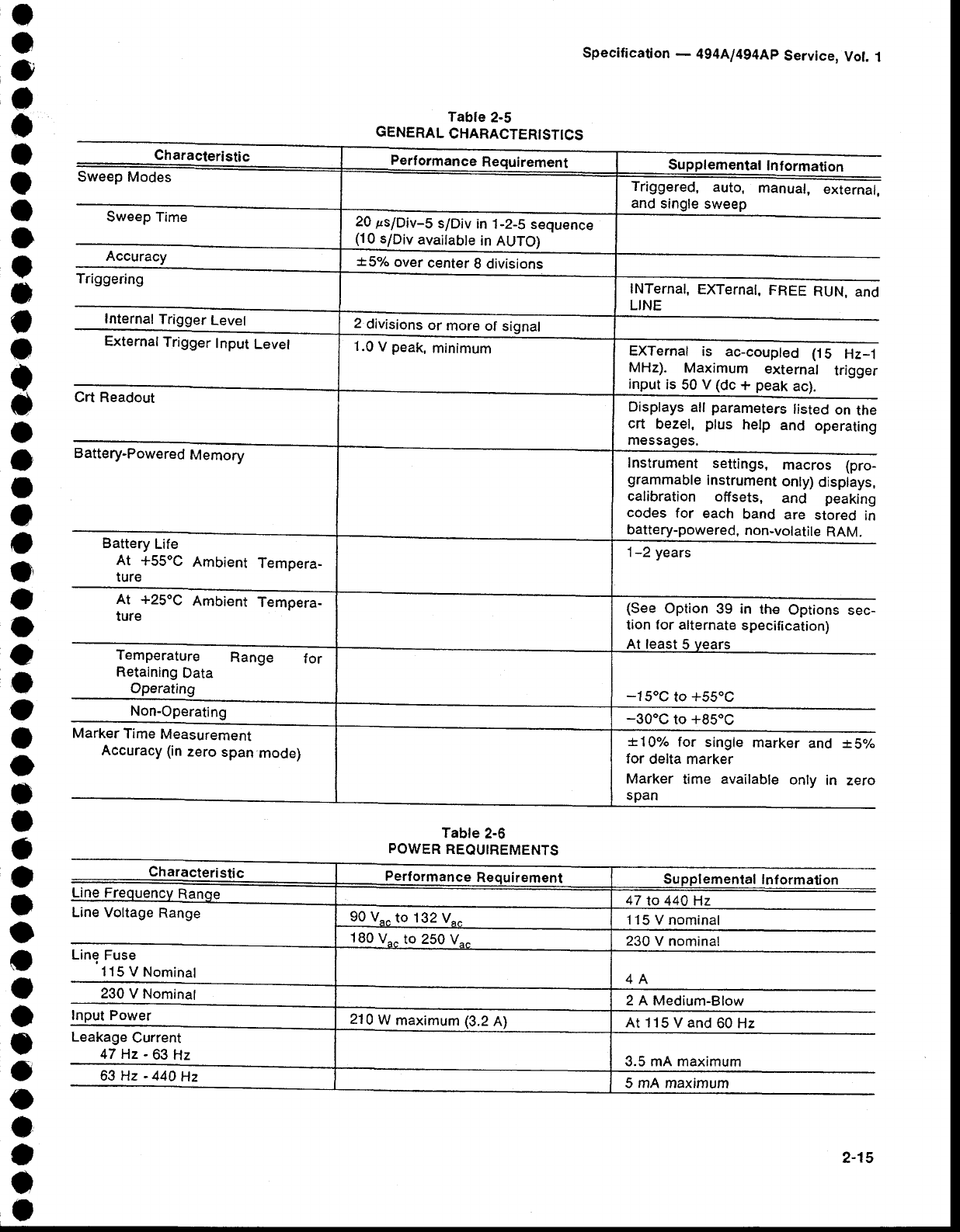
o
o
o
o
t
I
t
o
o
t
o
o
o
t
o
o
o
t
o
o
o
a
o
o
t
o
t
o
o
I
o
o
I
o
o
o
I
o
o
o
I
o
o
I
Characteristic
Sweep Modes
Sweep Time
Accuracy
Triggering
Internal
Trigger
Level
External
Trigger
Input
Level
Crt Readout
Battery-Powered
Memory
Battery
Life
At +55"C
ture Ambient
Tempera-
Tabte 2-5
GENERAL
CHARACTERISTICS
Table
2-6
POWER
REOUIREMENTS
Specification - 494A1494Ap
Service, Vol. 1
Information
Triggered,
auto,
and
single
sweep manual,
external,
lNTernal,
EXTernal,
FREE
RUN.
and
LINE
EXTernal is ac-coupled (1
5 Hz-1
MHz). Maximum external trigger
input
is
50
V (dc
+ peak
ac).
Displays
all
parameters
listed
on
the
crt bezel,
plus help and operating
rnessages.
lnstrument
settings,
macros (pro-
grammable
instrument
only)
displays,
calibration offsets, and peaking
codes
for each
band
are stored
in
battery-powered,
non-volatile
RAM.
1-2
years
At +25"C
ture Ambient
Tempera- sec-
Temperature Range for
Retaining
Data
Operating
(See Option 39 in the Options
tion
for alternate
specification)
least
5
-1 5"C to +55oC
-30"C to +85"C
*.10"h for single marker and isyo
for delta
marker
Marker time available only in zero
span
Supplemenlal
Inf
ormation
47
lo 440 Hz
1 15
V nominal
230 V nominal
2 A Medium-Blow
At 115
V
and
60 Hz
3.5 mA maximum
Non-Operating
Marker
Time
Measurement
Accuracy
(in
zero
span
mode)
Characteristic
Line
Voltage
Range
Line
Fuse
115
V Nominal
230
V Nominat
Input Power
Leakage
Current
47Hz-63Hz
4A
Perf
orman
ce Requirement
20 ps/Div-S s/Div in 'l
-2-5 sequence
!],,.9
s/Div avaitable
in AUTO)
*57o
over
center
I divisions
2 divisions
or more of signal
1.0
V
peak,
minimum
90 V.^
to 132
V
180
V,^
to 250
V
210
W
maximum
(3.2
A)
63 Hz - 440 Hz 5 mA maximum
2-15

Speclfication
- 494A1494AP
Service,
Vot.
1
Table
2-7
ENVIRONMENTAL
CHARACTERISTICS
Vibration (operating)
(instrument
secured
to a vibra.
tion
platform
during
test)
Meets
MIL
T-28800C,
type class
3, style C specifications.
Characteristic Descr
Temperature
Operating and
Humidity -15oC to +55oC/95"/"
(t 5o/" relative humidity).
Non-operating -62"C
to
+85
"C
Altitude
Operating 15,000
feet
(tested
to
25,000
fee$
Non-operating 40,000
feet
(tested
to
50,000 feet)
H
umidity
(non-operating) Five
cycles
(120
hours)
in accordance with MIL-Std-8l0
Procedure
lll {modified)
MIL-Std-810D,
Method
514, Procedure
| (modlfied).
Resonant
searches along
all
three axes from
5 Hz
to 15
Hz at 0.060-inch
displacemenltorT
minutes,
15 Hz
to 25 Hz at 0.040-inch
displacement
for 3 minutes, and 25 Hz to 55 Hz at
0.020-inch
displacement
for 5 minutes
(tested
to 0.025 inch).
Additional
dwellfor
10 minutes
in each
axis at the frequency of the major resonance
or at 55 Hz if
none
was found. Resonance
is defined
as twice the input displacement.
Total
vibration
time is approximately
75 minutes.
Shock
(operating
and non-operating) Three
guillotine-type
shocks
of 309,
one-half sine, 11
ms duration
each
direction
along
each major
axis for a total
of 18
shocks
(tested
to 509).
Transit
drop
(free
fall) One 8-inch
drop on each of six faces and eight corners (tested
at and meets
drop height of 12 inches).
Electromagnetic
lnterference
(EMl)
Conducted Emissions
Meets
requirements
described in MIL-Std-461
B, Part 4, except
as noted.
1 kHz
to 15 kHz only
15 kHz
to 50
kHz,
relaxed
by
15 dB
Conducted
Susceptibility Fulltimit
Fulllimit
Fulllimit
Radiated
Emissions Relaxed by 10 dB for fundamental
1oth harmonic of power
line
Exceptioned,
30 kHz
to 36 kHz
Fulllimit
Radiated
Suscepti
bility Fulllimit
To 5
A only
up to
1
GHz
aAfter storage at temperatures below -1soc, the instrument may not reset when power is first turned on. It this happens,
allow the
instrument
to warm up {or at least 15 minutes,
then turn the power off for 5 seconds and back on.
Remarks
to
CE01
- 60
Hz to 15
kHz
CE03-15 kHz
to 50 MHz
power
leads
CS01-30 Hz to 50 kHz
power leads
CS02-50 kHz to 400 MHz power
leads
CS06-spike power
leads
RE01*30 Hz to 50 kHz magnetic field
(measured
at 30 cm)
RE02-14 kHz to
10 GHz
RS01
-30 Hz
to
50
kHz
RS02
- Magnetic lndu6tion
RS03-14 kHz
to
10
GHz
2-16
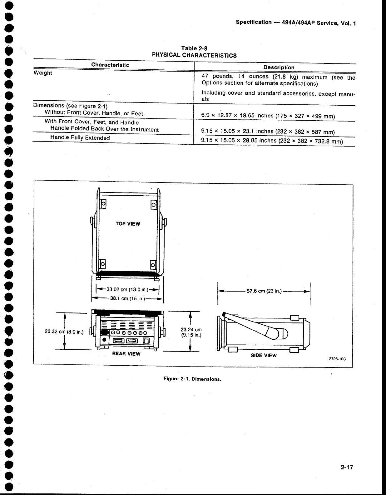
o
I
a
o
,
t
a
o
o
o
)
I
o
t
o
I
o
o
o
J
a
a
O
o
o
t
a
o
I
t
o
o
o
o
o
o
o
o
J
o
o
o
o
,
Characieristic
Weight
Dimensions
(see
Figure
2-1)
Without
Front
Cover,
Handle,
or Feet
With
Front
Cover,
Feet,
and
Handle
Handle
Folded
Back
Over
the
lnstrument
Handle
Fully
Extended
Specificaiion - 494A1494Ap
Service, Vol. 1
Table 2-8
PHYSICAL
CHARACTERISTTCS
Descriotion
47 pounds,
14 ounces
(21.8
kg) maximum
lsee the
Options
section
for alternate
specifications)
Including
cover
and standard
accessories,
except
manu-
at>
6.9
x 12.87
x 19.65
inches (175
x 327
x 499
66;
9,15
x 15.05
x 23.1 inches (282
x 382
x 567
p1r1
9.15
x '15.05
x 28.85 inches (232 x 392
x 732.g
mm)
Figure
2-1 - Dimensions.
l---t7'6cm(23''-
20.32
cm
(8.0
in.) 23.24 cm
(9.15
in-)
srDE
vtEw 2726-10C
2-17

o
a
o
I
c
t
t
o
o
a
o
I
o
t
o
c
o
t
o
o
a
a
o
o
I
I
o
o
a
t
o
o
o
o
o
o
o
o
f
o
o
a
I
o
a
O
o
a
o
o
I
I
o
t
I
)
I
o
a
I
a
o
o
a
o
o
o
o
o
a
o
o
I
o
o
O
I
o
a
a
o
a
o
o
o
O
o
o
Section
3 - 494A1494Ap
Service,
Vot.
I
INSTALLATION
This section describes unpacking, installation,
pow€r requirements,
storage
information
and repackag-
ing for the spectrurn
analy;er.
UNPACKING
AND
INITIAL
INSPECT|6N
.. Bglorg unpacking
the spectrum
analyzer,
inspect
the shipping
container
for signs
of externat
damage.
lf
the container
is damageO,
nbtity
the carier as well
as
Tektronix, Inc. The shipping Lontainer contains the
basic
instrument
and its standard
acc€ssories.
For a
list of the standard
accgssori€s,
refer to Section
1 of
this manual (or,
for ordering
information,
refer
to the list
following
the Replaceable
Mechanical
parts list in the
Service
Manual,
Volume
2).
lf the contents
of the shipping
container
are
incom-
plete,
if there is mechanical
damige or defect,
or if the
instrument
does not meet operational
check require-
rnents, contact your local Tektronix Field Office or
representative.
Keep
the shipping
container
if the instrument
is to
be
-stored^
or shipped
to T€ktronix
tor service
or repatr.
Refer
to Storage
and
Repackaging
for Shipment
later
in
this
section.
The instrument
was inspected
both mechanically
and electrically
before
shipment,
and it should
be free
of mechanical
damage
and
meet
or exceed
all
electrical
specifications.
Th€
Operation
section
of the Operators
Manual contains procedures
to check functional
or
operational
performance. perform the functional
check
procedure to verify that the instrument is operating
properly.
This
check
is intended
to satisfy
the require-,
ments
for most receiving
or incoming
inipections. {A
detailed
electrical performance
veriticition
procedure
in
the Performance
Check
section
of this manual
provides
a check of afl specified pertormance
requirements,
as
listed
in
the
Specification
section.)
The instrument
can
be operated
in any
position
that
allows air flow in the bottom and out the rear of the
instrurnent. FEet on
the four corners
allow
ample
cfear-
ance
sven
if the instrument
is stacked
with
other
instru_
ments. The air is drawn in by a fan through
the bottom
and expelled out th€ back Avoid locating
the instru_
ment where paper,
plastic,
or any other material
might
block
the
air
intake.
The front cover
provides
a dust-tight
seat
and
a con_
venient place to store accessories and extemal
waveguide
mixers. Us€ the cover to protect the front
panel
when storing
or transporting
the instrument.
To
removs
the cover,
stand
the instrument
on the
h^/o
back
feet so the name on the handle is facing up and
towards
you,
and
pull
slightly
out
and
up on
the sides
of
the cover. Attached
to the inside
of the cover
is the
accessories
pouch. To open the accessories pouch,
pull
up
evenly
on
the flap.
You can position the handle of the spectrum
analyzer
at several
angles
to serve
as a tilt stand. To
stack
instruments, position
the handle
at
the
top rear
of
the instrument.
To change
the handle
position,
press
in
at both pivot points
and rotate
the handle
to the desired
position.
Removing
or replacing
the cabinet on the
instrument can be hazardous. Only
qualified
service
personnel
should attempt
to rernove
the instrument
cabinet.
3-1
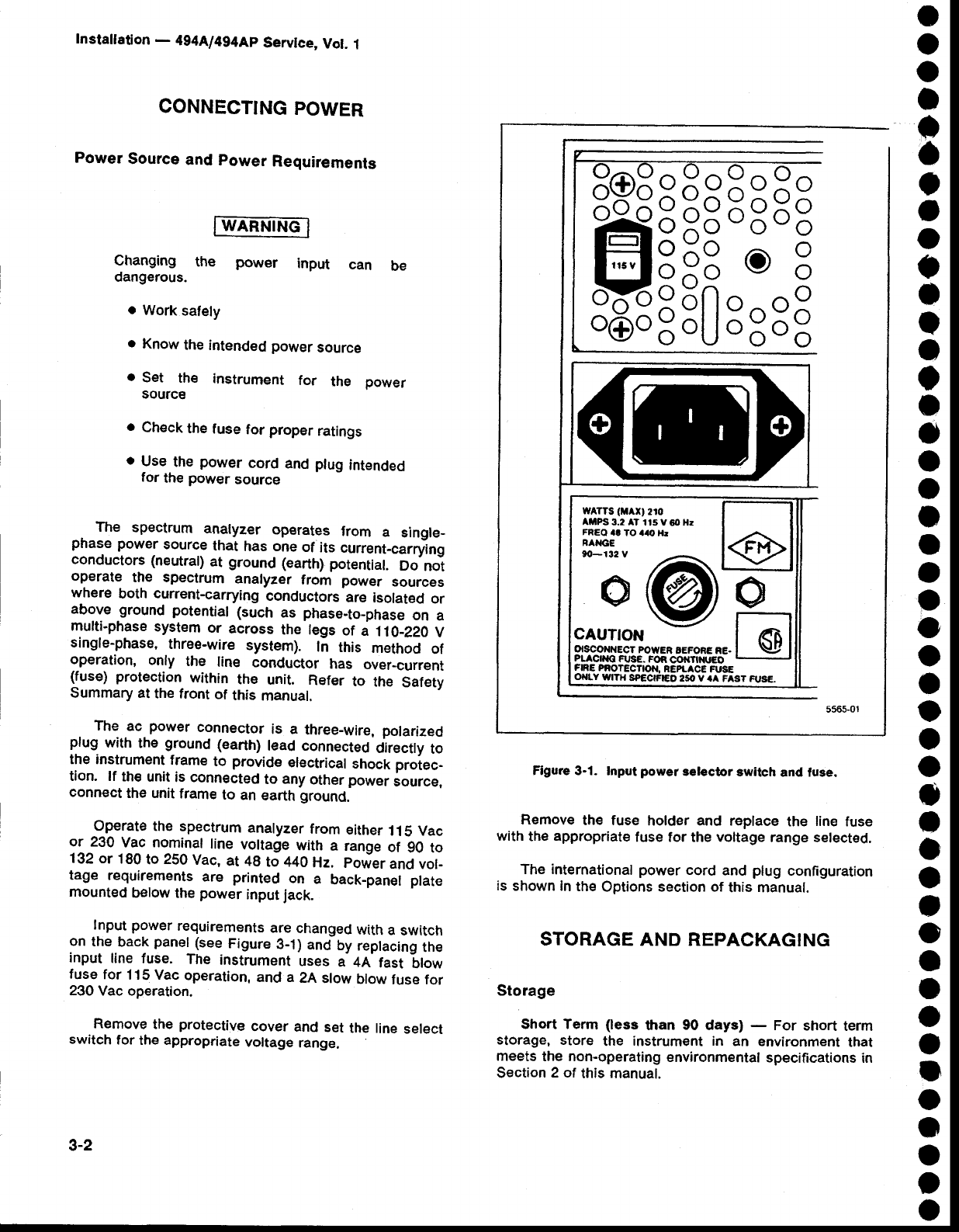
Installation
- 494A/494Ap
Servlce,
Vol.
1
CONNECTING
POWER
Power
Source
and
power
Requirements
o
a
o
I
a
a
o
o
O
a
o
a
o
I
I
o
o
o
t
o
a
o
o
o
o
O
o
o
o
o
o
O
o
o
a
o
o
o
o
o
o
o
)
a
g-2
Changing the powef input can be
dangerous.
o Work
safely
o Know
the intended
power
source
o Set the instrument for the power
source
o Check
the
fuse
for proper
ratings
. Use
the power
cord and
plug
intended
for
the
power
source
The spectrum analyzer operates from a single_
phase
power
source
that
has one
of its curent-carrying
conductors
(neutral)
at ground
(earth)
potentiat.
Oo-no-t
operate the spectrum
analyzer
from power sources
where both current-carrying
conductors
are isolated
or
above ground
potential
(such
as phase-to_phase
on a
multi-phase
system
or across
the legs
ot a fiA-220 y
single-phase,
three-wire
system). tn tms method of
operation,
only the line conductor has over_current
(fuse) protection
within the unit. Refer
to the Safety
summary
at
the
front
of this
manual.
The ac power
connector
is a three_wire,
polarized
plug with
the ground
(earth)
lead connected
direcfly
to
the instrument
frame
to provide
electrical
shock
proiec-
tion. lf th€
unit
is connected
to any
other
power
source,
connect
the unit
frame
to an
earth
ground-
Operate the spectrum
analyzer
from
Either
11S Vac
or 230 Vac nominal
line voltage
with a range
of 90 to
132
or 180
to 250
Vac,
at 4g to 440
Hz. power
and
vol_
tage requirements
are printed on a back_panel plate
mounted
below
the
power
input
jack.
tnput power
requirements
are
changed
with
a switch
on the back
panel
(see
Figure
3-1)
and
by
replacing
the
input line fuse. The instrument
uses a 4A fast blow
fuse
for 115 Vac
operation,
and a 2A
slow
blow
fuse for
230
Vac operation.
Remove
the protective
cover
and
set
the line
select
switch
for
the appropriate
voltage
range.
Figure 3-1. Input
power
selector
switch
and fuse.
Remove
the fuse holder and replace
the line
fuse
with
the
appropriate
fuse for the voltage
range selected.
The international power
cord and plug
configuration
is
shown in
the
Options section of
this manual.
STORAGE AND REPACKAGING
Storage
Short Term (less
than 90 days) - For short
term
storage,
store the instrum€nt in an environment
that
meets
the non-operating
environmental
specitications
in
Section
2 of this manual.
o
o
o
o
o
o
o
o
o
o
o
o
o
0
335
O
3s3
o
o
o
o
o
o
o
o
o
o
o
o
o
o
o
WATTS
([AXl 210
AMPS 3.2 AT 1'ls Y 60 Hr
FREO a! TO i|'.o X!
FANGE
90-132 V
o@
CAUTION
FIRE FUI
OilLY WITH 250 Y aA
r POWER
IEFORE NI
tE
:AST
FUSe.
o
o
o
o
o
o
o
o
o
o
o
a
o
o
o
o
o
o
o
o
o
o
O
o
a
o
o
o
o
o
a
o
O
o
o
o
o
a
o
o
o
o
o
o
Long
Term
- For instrument
storage
of more
than
90 days,
retain
the shipping
container
ti iepacXage
ttre
instrument.
The battery in tt e instrume-rit
does not
require
rernoval. package
the instrument
in a vapor
barrier
bag with a drying
agent
and
store'in
a tocation
rnat meets the non-op€rating environmental
specifications
in Section
2 of this
manlal.
|f Lgr. l1o: any questions,
contact
your
tocat
Tek-
tronix
Field
Office
or representative.
Repackaging for Shipment
_ .
Whgn
the spectrum
analyzer
is to be shipped
to a
Tektronix
Service
Center
for service
o, ,"j"ir, attach
a
tag
that
shows
the
owner
and
address,
the
name
of the
individual
at your firm
that can
be contacted,
the com_
plete
instrument
serial
number.
and
a description
of the
service
required.
lf the
original
package
is unnt for use
or not
available,
use
the
following
repickaging
informa_
tion.
Instaltaton
- 494[l4g4Ap
Service,
Vol.
1
1.
To allow for cushioning,
use a corrugated
cardboard container with a test strengttr oi gZS
pounds
(140
kilograms)
and inside
dimensions
that
are at least six inches more than the equipment
dimensions
(refer
to the physical
Characteristics
in
Section
2).
2. Install
the instrument
front
cover,
and
surround
the instrument with plastic sheeting
to protect the
finish.
. 3. Cus.hion
the
equipment
on all sides
with
pack-
ing
material
or plastic
foam.
4. Seal the container
with shipping
tap€ or an
industrial,
heavy-duty
stapler.
3-3

O
o
o
o
o
a
o
o
o
O
o
o
o
o
o
o
o
o
o
o
O
o
o
o
c
o
O
o
o
o
a
o
o
O
O
o
o
o
I
o
o
o
o
o
PERFORMANCE
CHECK
Introduction
All performance
checks are carried out without
removing
the
instrument
covers.
The
procedures
in this
section
verify
that
the
instru-
ment performance
satisli€s
the performance
require-
rnents specified
under the performance
Requirement
column
in
Section
2, Specification.
Some
parameters
and
instrument
functions
that are
not explicitly
specified
are
also
checked.
These
checks
verify
that
the
instrument
performs
as described.
Checks
should
be performed
in sequence
because
som€ tests rely on the satisfactory
performance
of
related circuits. Also, the cneck iteps have been
arranged
so
that
the changing
of test
equipment
setups
from
one
step
to the
next
is minimized.
lf a measurement
is marginal
or below
specification,
an adjustment
procedure
to enhance
performance
will
be
found,
under
a similar
treading,
in
Section
5,
Adjust-
ment
Procedure.
After
adjustment,
recheck
the perfor_
mance.
Adjust
only
those
circuits
that
do not
meet per-
formance
criteria.
lf adjustment
fails to return
the circuit
to specified
performance,
refer to the Maintenance
section for
troubleshooting
and
repair
procedures.
Incoming
Inspection
Test
The Operators
manual
contains
an operational
or
functional
check
that
checks
all
functions.
This
eheck
is
recommended
for incoming
inspections
because
it
requires
no
external
equipment
or
special
expertise
and
is a reliable
indication
that
the
instrument
is perforrning
properly.
Option Instrument
Checks
. Whenever
practical,
performance
checks
for option
instruments
are integrated
in the performance
check
steps for the standard
instrument,
otherwise
special
check-steps
are provided
under OPTION
INSTRU-
MENTS
towards
the
back
of
this
section.
o
o
o
O
o
o
o
o
o
o
o
o
o
o
o
o
o
o
o
o
o
o
O
o
o
o
o
o
o
o
o
o
o
o
o
o
o
o
o
o
o
o
o
o
Secton 4 - 4g4Al494Ap
Service
Vol. 1
Verification of Tolerance Values
Compliance
tests, of those limits
listed
in
the
p€rfor-
mance Requirement column of the instrum€nt
specifications,
shall
be
perform€d
after
sufficient
warm-
up
time and
comptetion
of preliminary
pr€paration
steps
(such
as
front-panel
adjustments).
Measurement
tolerance
of test eguipment
should
be
negligible
in comparison
to the
specified
tolerance;
and,
when not negligibte,
the error of the measuring
apparatus
shall
be
added
to the
tolerance
specified.
History
Information
The instrument and manual are periodically
evaluated and updated. lf modifications
require
changes
in the procedures,
information
applicable
to
earlier
instruments
wil be
included
within
a step
or as
a
sub-part
to a step.
Equipment
Required
Table
4-1 lists the test equipment
and calibration
fixtures
recommended
for
the
performance
Check,
This
equipment
is also applicable
for the adjustment
pro_
cedures in Section 5, Adjustment
procedure. The
equipment
characteristics
specified
are the minimum
required
for the checks. Substitute
equipment
must
meet
or exceed
these characteristics.
These
fixtures
are
available
from Tektronix,
Inc.,
and may
be ordered
through
your local
Tektronix
Field
Office or representa-
tive.
Some checks may not be practical
because
they
may require
sophisticated
test equipment
and/or
pro-
cedur€s.
In those
cases, a compromise
may be
made
in the procedures.
When
that occurs,
a statement
or
footnote
to that fact is added
to the step. The more
exact method
of measuring
the characteristic
can be
supplied
by
your
Tektronix
Service
Center.
4-1
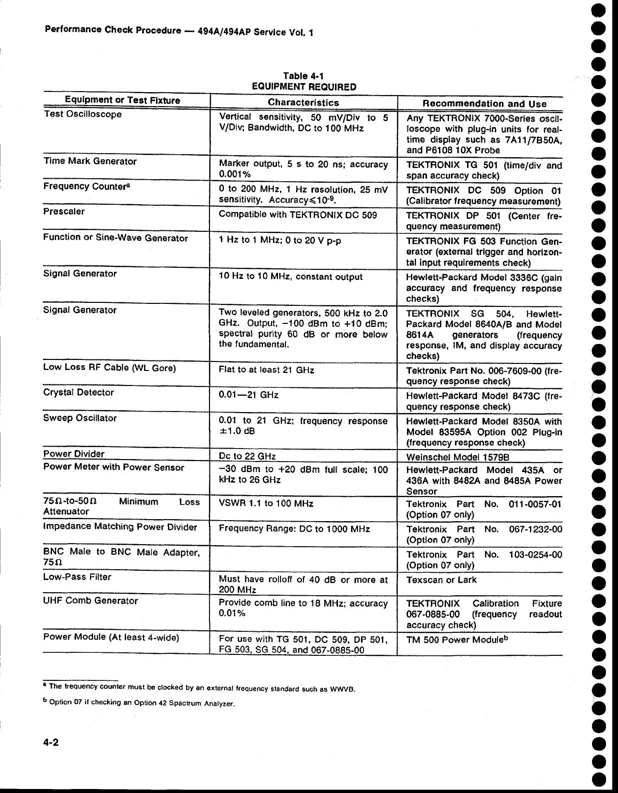
Performance
Check
Procedure
- 494A/4g4Ap
Service
Vol.
1
Table
4-1
EOUIPMENT
REOUIRED
or Test
Flxture
Test Oscilloscope
Time
Mark
Generator
Frequency
Countera
Prescaler
Function
or Sine-Wave
Generator
Signal Generator
Signal
Generator
Low Loss RF Cable (WL Gore)
CrystalDetector
Sweep Oscillator
Power Meter
with
Power
Sensor
750-to-50(} Minimum Loss
Attenuator
lmpedance
Matching
Power
Divider
BNC MAIE tO BNC
75() Male Adapter,
Low-Pass Filter
UHF Comb
Generator
Power Module (At least 4-wide)
I The frequency counter must b€ clocked by an external frequency standard such as wwvB.
b Option 07 it checking en Option 42 Spactrum Analyzer.
4-2
Recommendation
and Use
Any TEKTRONIX
7000-Series
oscil-
loscope with plug-in
units
for real-
time display
sueh
as 7A11/7850A,
and
P6108
10X
Probe
TEKTRONIX TG 501 (time/div
and
span
accuracy check)
TEKTRONIX
DC 509 Option 01
(Cal
ibrator
f requency
measurement)
TEKTRONIX DP 501 (Center fre-
quency
measurement)
TEKTRONIX FG 503 Function
Gen-
erator (external
trigger and horizon-
tal input requirements
check)
Hewlett-Packard
Model
3336C
(gain
accuracy and frequency
r€sponse
checks)
TEKTRONIX SG 504, Hewlett-
Packard
Model 8ilOA/B and Model
8614A generators (frequency
response, lM, and
display accuracy
checks)
Tektronix
Part
No. 006-7609-00
(fre-
quency
response
check)
Hewlett-Packard
Model
8473C
(tre-
response
check)
Hewlett-Packard Model
8350A with
Model 83595A Option 002 Plug-in
(frequency
response
check)
Weinschel Model 1
Hewlett-Packard Model 435A or
436A with 8/,82A
and 8485A
Power
Tektronix Part No.
(Option
07
only)
Tektronix Part No.
(Optlon
07
only)
Tektronlx Part No.
(Option
07
only)
Texscan or Lark
TEKTRONIX
067-088s-00
01 1
-00s7-01
067-1232-00
1
03-0254-00
Calibration Fixture
(frequency readout
o
o
o
o
o
o
o
o
o
o
o
o
o
o
o
o
o
o
o
o
o
o
o
o
o
o
o
o
o
o
o
o
o
o
o
o
o
o
a
o
o
o
o
o
accuracy
Vertical sensitivity,
50 mV/Div to
V/Div;
Bandwidth,
DC
to 100
MHz
Marker
output,
5 s to 20 ns; accuracy
0.001%
0 to 200 MHz,
1 Hz resolution, 25 mV
Compatible
with
TEKTRONTX
DC S09
1
Hz
to'l MHz;
0 to 20
V
p-p
10
Hz
to
't
0
MHz,
constant
output
Two
leveled
generators,
500 kHz to 2.0
GHz. Output,
-100 dBm to *10 dBm;
spectral
purity
60 dB or more below
the fundamental.
Flat
to at least
21
GHz
0.01 to 21 QHz; frequency
response
f 1.0
dB
-30 dBm
to +20 dBm tuil scale:
100
kHz
to 26
GHz
VSWR
1.1
to
100 MHz
Frequency
Range:
DC
to 1000
MHz
Must have
rolloff
of 40 dB or more
al
Provide
comb
line
to 18
MHz; accuracy
0.01%
For
use
with TG
501, DC
509,
DP
501,
FG
503,
SG 504. and
067-0885-00 TM 500 Power Moduleb
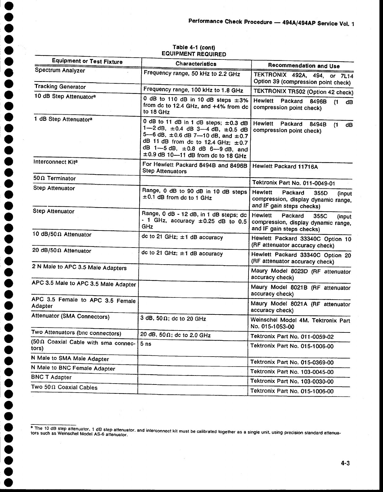
o
o
o
o
o
o
o
o
o
o
o
o
o
O
o
a
o
o
o
o
o
o
o
o
o
o
o
o
o
o
o
o
o
o
o
o
o
o
o
o
o
o
o
o
Performance
check procedure
- 4g4br4g4Ap
service vor. 1
Table
4-1
(cont)
EOUIPMENT
REOUIRED
Equipment
or
Test
Fixture
spectrum
Analyzer
Tracking
Generator
10
dB
Step
Attenuatora
dB step
Attenuatora
lnterconnect
Kita
50O Terminator
StepAttenuator-
st"pnttenui-
lodB/sooltt"ffi
20
dB/50O
Attenuator
-
2NMaretoApc@
APcg.5rt,tur"to@
APC 3.5 Female
to ApC 3.S
Femate
Adapter
Characteristics Recommendation and Use
Frequency
range,
50
kHz
to 2_2
GHz TEKTBONIX
492A, 494, or ZLIU;
Option
39
(compression
point
check)
Frequency
range,
100 kHz
to 1.9
GHz TEKTRONIX
TR502
(Option
42
check)
0 dB to 110 dB in 10 dB steps :L3yo
from dc to 12.4
GHz, and *4oh trom dc
to 18
GHz
Hewlett Packard 84968 (1 dB
compression
point check)
0 dB
to 11
dB in.t dB
steps;
*0.3 de
1-2d8, +0.4 dB g-4 dB, :r0.5
dB
5-6 dB,
*0.6 dB 7-10 dB, and
*0.7
dB 11
dB from
dc to 12.4
GHz;
*0.7
dB 1-5 dB, :b0.8
dB 6-9 dB, and
*0.9
dB
10-11 dB from
dc to
1g
GHz
Hewlett Packard 84948 (1 dB
compression point check)
For Hewlett packard 94948 and 94968
step Attenuators Hewlett Packard 1
1 2.1
6A
Tektronix
Part
No.
011-0049-01
Range,
0 dB to 90 dB in 10 dB steps
*0.1 dB from dc to 1 GHz Hewlett Packard g55D (input
compression,
display
dynamic
range,
and
lF gain
steps
checks)
Ra.nge!
0 dB - 12dB, in 1 dB steps;
dc
LrlrGtr, accuracy
*0.2s
dB
io 0.5 Hewlett Packard 355C (input
compression,
display
dynamic
range,
and
lF gain
steps
checks)
dc
to
21
GHz; *1 dB accuracy Hewlett
Packard
3gg40c Option
10
(RF
attenuator
accuracy
check)
dc to 21 GHz; +1 dB accuracy Hewlett
Packard
ggg4oc Option
20
(RF
attenuator
aceuracy
check)
Maury Model 8023D (RF attenuator
accuracy
check)
Maury Model 80218 (RF attenuator
accuracy
check)
Maury Model 8021A
(RF attenuator
accuracy
check)
Arlenuator
(sMA
connectors)
Two
Attenuators
(bnc
connectors)
3
dB,
50o; dc
to 20
cHz Weinschel
Model
4M. Tektronix
part
No.015-1053-00
20
dB,50o; dc to 2.0
GHz Tektronix
Part
No.
011-00S9-O2
(5url uoaxtal cable with sma connec-
tors) 5ns Tektronix
Part
No.
015-1006-00
N Mate
to sMA Male Adapter Tektronix
Part
No.
015-0369-00
N Mate
to BNC
Female
Adapter Tektronix
Part
No.
103-0045-00
UNU I Adapter _
Two 50O Coaxial
Cables Tektronix
Part
No.
103-0030-00
Tektronix
Part
No.
015-1006-00
8 The 10 dB step attenuator' 1 d-Bstep attenuator. and interconnect kit must be calibrated iogether as a single unit. using p(ecision standard attenua-
tors such as Weinschel Model AS_6
attenuator.
4-3
Performance
Check
Procedure
- 4g4Ll4g4Ap
Servlce
Vol.
1
PRELIMINARY
PREPARATION
o
o
o
o
a
o
o
o
o
o
o
o
o
o
O
o
o
o
o
o
o
o
o
o
o
o
o
o
o
o
o
o
o
o
O
o
o
o
o
o
o
o
o
o
4-4
lnitial Power-Up
During
initial
power-up
cycle,
the instrument
type,
instrument
operating
system
processor
firmware
ver_
sion,
and
the front panel
processor
firmware
versions
are
displayed
on
the crt for approximately
two seconds.
The
Replacement
Parts
List
in the
Serviie manual,
lists
the ROMs
used
for each version. The service
manual
also
lists
the firmware
operating
notes
associated
with
each
firmware
version.
lf the microcomputer
detects
a hardware
failure.
a
failure
report
will come
on screen
and remain
for about
2 seconds. A status message
will then appear
and
remain
for the duration
of the failure. press <Blue_
SHIFT> MAX HOLD to bring eror messages
to the
screen.
a. Connect
the
spectrum
analyzer power
cord
to an
appropriate power source
(refer
to power Source and
Power Requirements
in Section
g, Installation).
Set
TIME/DIV
to AUTO
and switch
pOWER
on.
b. When
POWER
is sivitched
oR,
the pOWER
indi-
cator
(a green
LED)
should come
on.
c. The
microprocessor
runs
a memory
and
UO
t€st.
lf no
processor
system
problems
are
found,
the
power-
up
program
will complete
in approximately
10 seconds,
and
the instrument
wilt be ready
to operite. After
the
power-up
routine,
the crt will initiatize
as shown
in Fig-
ure 4-'l
.
d. The operating
functions and modes should
initial-
ize to th€ following state:
Readout
REF
LEVEL
CENTER FRECIUENCY
MARKER
FREQUENCY
sPAN/DrV
VERT
DISPLAY
RF ATTEN
FREO RANGE
REF
OSC
RESOLUTION
BANDWIDTH
TRIGGERING
AUTO RESOLN
DIGITAL
STORAGE
MIN
NOISE
All
other
pushbuttons
On
ODBM
0.90GHZ
0.00GHz
MAX
10DB/
2ODB
0-1.8a
t-ub
3MHZ
FREE RUN
On
VIEWA&VIEWBon
On
lnactive or off
e. Set the MIN
RF ATTEN
dB controt
to 0 (NORM)
and
th€ PEAK/AVERAGE control
fully
counterclockwise.
set the
TlMEiDlv control
to AuTo, REF
LEVEL
to read
-20DBM, and adjust th€ INTENSITY control
for the
desired
brightness.
Note
that the
RF ATTEN
readout
is
now
0DB.
f. Apply the CAL OUT signal to the RF INPUT
through
a 50O cable
and a N-TO-BNC adapter.
g, A dot marker
will appear
in the upper
portion
of
the screen in the MAX
frequency mode. This marker
indicates
the
location
on
the display to which
the spec-
trum analyzer frequency
is tuned, With a frequency
readout
of 0.00GH2,
the marker will be
in
the
upper left
portion of the screen. Rotate
the CENTER/MARKER
FREQUENCY control and note that the dot marker
moves across the display. Notice that the oENTER
FREOUENCY readout
(top line) remains
at 0.90GH2,
and that the MARKER
FREOUENCY
readout
(second
line) changes
according
to the position
of the marker
(dot).
h. Harmonics
of the
100
MHz
calibrator
signal
will
be displayed
as shown
in Figure 4-2. To select 100
MHz
center frequency,
press
the
pushbutton
sequence
of <Blue-SHIFT>
FREO'100
MHz.
i. To change
the SPAN/DIV
to 100
MHz,
press
the
pushbutton
sequence
of <Blue-SHIFT>
SPAN/DIV 100
MHz. The
dot marker is now
horizontally
centered,
and
the 100 MHz
calibrator
signal is at
center screen.
aGHz
btntEnNeL UNLOCK:
Most lrequency
measurements
will not be
accurate
unlil
after this
readout
has
changed
to lNT.
rE a.SlC TI
a
-tt
-n
{
{
{
-
-t
-
4E
j
55€{t24
Figure
4-1. Grt
disptay
at initial
power-up.
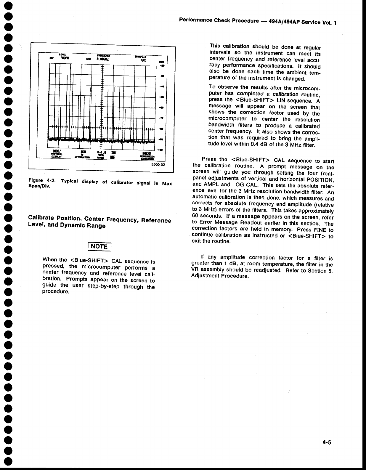
E -28( o a.
s
r
rotx f,
-t
{
{
{
-
-r
-
-
-ta
.C DII
I
I
t'
I
ssqx2
o
o
o
o
o
o
o
o
o
O
o
o
o
o
a
o
o
o
o
o
o
o
o
o
o
o
o
O
o
o
o
o
o
o
O
a
O
o
o
o
o
O
a
o
Performance
Check
procedure
- 4g4Ll4g4Ap
Service
Vol. 1
Figure -4-2. Typical display of catibrator signat In Max
Span/Div. i
Calibrate
Position,
Center
Frequency,
Reference
Level,
and
Dynamic
Range
This calibration
should
be done
at regular
intervals
so the instrument
can meet its
eenter
frequency
and reference
level
accu_
racy performance
specifi,cations.
lt should
also be done each time the ambient
tem-
perature
of the instrument
is
changed.
To observe
the results
after
the microcom-
puter has cornpleted
a calibration
routine,
press
the <Blue-SHIFT>
LIN
seguence.
A
message
will appear on the screen
that
shows the correction
factor used by the
microcomputer
to center the resolution
bandwidth
filters to produce
a calibrated
center
frequency.
lt also
shows
the
correc-
tion that was required
to bring
the ampli_
tude
level
within
0.4
dB of the
3 MHz
filter.
Press
the <Blue-SHIFT> CAL sequence
to start
the calibration
routine. A prompt message
on the
screen
will guide you through
setting
the four front-
panel
adjustments
of vertical
and
horizontal
pOSlTlON,
and
AMPL
and
LOG
CAL. This
sets
thE absolut€
refer_
ence
level
for the 3 MHz
resolution
bandwidth
filter. An
automatic
calibration
is then
done,
which
measures
and
corrects
for absolute
frequency
and
amplitudo
(r€lative
to 3 MHz)
errors
of the filters. tnis takes approximately
60
seconds.
lf a message
appears
on
the screen,
rsfer
to Error
Message
Readout
earlier
in this section.
The
correction
factors
are held in memory.
press FINE
to
continue
calibration
as instructed
or <Blue_SHIFT>
to
exit
the
routine.
lf any amplitude
correction
factor for a fitter is
greater
than
1 dB. at roorn
temperature,
the tilter
in
the
VR
assembly
should
be readjusted.
Refer
to Section
S.
Adjustment
Procedure.
When
the <Blue-SHIFT>
CAL
sequence
is
pressed, the microcomputer
pe*orms a
center
frequency
and reference
level cali-
bration. Prompts
app€ar
on the screen
to
guide
.the user step-by_step
through the
procedure.
4-5
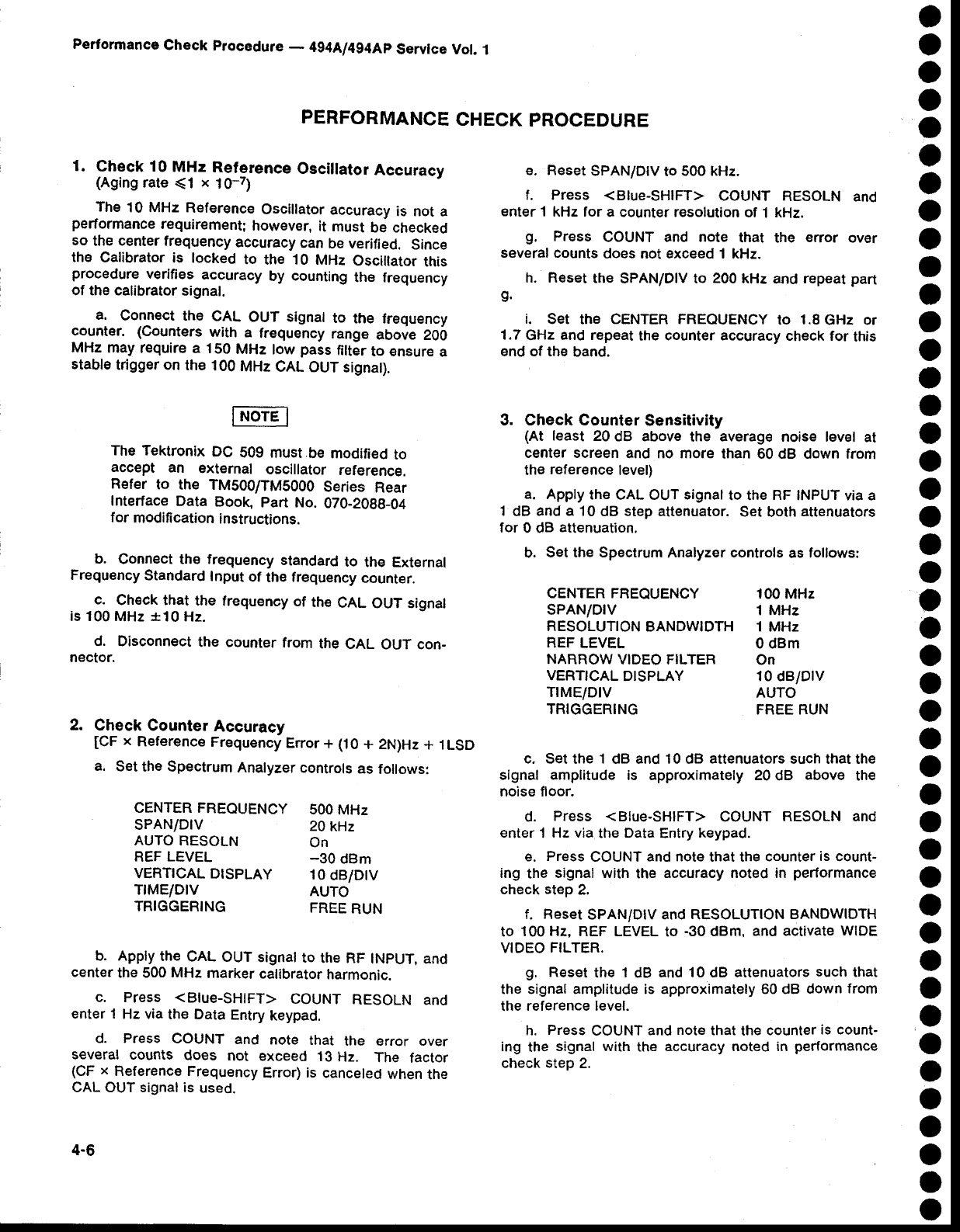
Performance
Check
Procedure
- 4g4Ll4g4Ap
Servlce Vot.
.l
PERFORMANCE
CHECK
PROCEDURE
1. Check 10 MHz Reference
Oscillator
Accuracy
(Aging
rate
<1 x 10⁻⁷)
The
10 MHz Reference
Oscillator
accuracy
is not
a
performance
requirement;
however,
it must
be checked
so
the
center frequency
accuracy
can
be verified.
Since
the calibrator
is locked
to the 10 MHz oscillator
this
procedure
verifies
accuracy
by counting
the frequency
of the
calibrator signal.
a. Connect the CAL OUT signal
to the frequency
counter. (Counters
with a frequency
range
above
200
MHz
may
require a 150
MHz
low
pass
filter
to €nsure
a
stable
trigger on
the 100
MHz
CAL
OUT
signat).
The Tektronix
DC 509
must.be
modified
to
accept an external oscillator reference.
Refer to the TMS00ffM5000
Series Rear
Interface Data Book, part No. 070-2099_04
for modifi
cation
instructions.
b. Connect the frequency
standard
to th€ External
Frequency
Standard
Input
of th€
frequency
counter.
c. Check that the frequency
of the
GAL
OUT signat
is 100
MHz
*10 Hz.
d. Disconnect
the counter
from
the
CAL OUT
con_
nector.
e. Reset
SPAN/DIV
to 500 kHz.
f. Press <Blue-SHIFT>
COUNT
RESOLN
and
enter
1 kHz for a counter resolution
of 1 kHz.
g. Press COUNT and note that the error over
several counts
does not exceed 1 kHz.
h. Reset
the sPAN/Dlv to 200
kHz
and
repeat part
g.
i. SEt thE CENTER FREOUENCY
tO 1.8
GHZ Or
1.7
GHz
and repeat
the
counter accuracy
check for this
end of the
band.
3. Check Counter Sensitivity
(At least 20
dB above
the average
noise level at
center screen
and no more
than 60 dB down from
the
refer€nce
level)
a. Apply
the
CAL OUT
signal
to the
RF
INPUT via a
1 dB and a 10
dB step attenuator.
Set
both
attenuators
for 0 dB attenuation.
b. Set the Spectrum
Analyzer
controls
as
follows:
o
o
o
o
o
o
o
o
o
o
a
o
o
a
o
o
o
o
o
o
o
o
o
o
o
o
o
o
o
o
o
o
o
o
a
O
O
o
o
o
o
o
o
o
CENTER FREOUENCY
sPAN/DrV
RESOLUTION
BANDWIDTH
REF
LEVEL
NARROW
VIDEO FILTER
VERTICAL
DISPLAY
TrME/DtV
TRIGGERING
100
MHz
1 MHz
1 MHz
0 dBm
On
10 dB/Drv
AUTO
FREE RUN
2. Check
Counter
Accuracy
[CF
x gslslsnce
Frequency
Error
+ (10
+ 2N)Hz
+ l LSD
a. Set
the Spectrum
Analyzer
controls
as
follows:
b. Apply
the
CAL
OUT
signat
to the RF
lNpUT, and
center
the 500
MHz
marker
calibrator
harmonic.
c. Press <Blue-SHtFT>
COUNT
RESOLN
and
enter 1 Hz via
the Data
Entry
keypad.
d. Press
COUNT
and note that the error over
several
counts does not exceed .lSHz. The factor
(CF
x Reference Frequency
Error)
is
canceled
when
the
CAL OUT signal is
used.
4-6
c, Set the 1 dB and 10 dB attenuators
such that the
signal amplitude is approximately 20 dB above the
noise floor.
d. Press <Blue-SHIFT> COUNT RESOLN and
enter
1 Hz via
the Data
Entry
keypad.
e. Press
COUNT
and note
that the counter
is count-
ing the signal with the accuracy noted in performance
check
step
2.
f. Reset
SPAN/DIV ancl RESOLUTION
BANDWIDTH
to 100
Hz, REF LEVEL
to -30
dBm, and activate
WIDE
VIDEO
FILTER.
g, Reset the 1 dB and 10 dB attenuators
such
that
the signal amplitude is approximatety 60 dB down
from
the reference level.
h. Press
COUNT
and
note
that
the counter
is count-
ing the signal with the accuracy noted in performance
check
step
2.
CENTER FREOUENCY
sPAN/DrV
AUTO RESOLN
REF
LEVEL
VERTICAL
DISPLAY
TrME/DrV
TRIGGERING
500
MHz
2AkHz
On
-30 dBm
10
dB/Dlv
AUTO
FREE
RUN
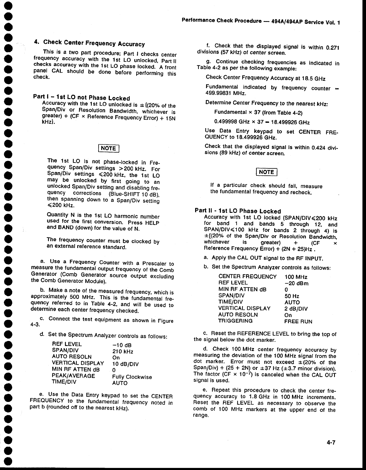
o
o
o
o
o
o
a
o
o
a
o
a
o
o
o
I
a
o
o
o
o
I
o
o
o
o
o
O
I
I
o
o
O
o
I
I
o
O
O
o
a
o
o
o
4. Check Center Frequency Accuracy
. This is a two part procedure;
part I checks
center
frequency
accuracy
with the 1st LO unlocked,
part
ll
checks
accuracy
with
the l st LO phase
lockecl.
A front
panel CAL should be done before performing
this
check.
Part
| - lst LO not phase Locked
Accuracy
with
the
.l
st LO
unlocked
is :r {(20% of
the
Span/Div
or Resolution
Bandwidth,
whichever
is
g.relter)
+ (CF x Reference
Frequency
Eror) + 15N
kHz).
The 1st LO is not phase_locked
in Fre_
quency
Span/Div
settings
>200 kHz. For
Span/Div
settings
(200t<Hz,
the 1st LO
may be unlocked by first going to an
unlocked
Span/Div
setting
anO
Oisa6ling
tre-
quency corrections (Btue-SHtFT
t
0
dB),
then spanning
down
to a Span/Div
setting
(200 kHz.
Quantity
N is the 1st
LO harmonic
number
used
for the first conversion.
press HELp
and
BAND
(down)
for
the
value
of N.
The frequency
counter
must
be clocked
by
an
external
reference
standard.
a. Use a Frequency
Counter
with a prescaler
to
measure
the
fundamental
output
frequency
of the
Comb
Generator
(Comb Generator
source output excluding
the
Comb
Generator
Module).
b. Make
a note
of,the
measured
frequency,
which
is
approximately
500 MHz. This is the fundamental
fre-
quency
referred
to in Tabte
4-2, and
will be used
to
determine
each
center
frequency
checked.
c. Connect
the
test
equipment
as shown
in Figure
4-3.
d. Set
the
Spectrum
Analyzer
controls
as
follows:
REF
LEVEL -10 dB
SPAN/DIV 210
k:Hz
AUTO
RESOLN On
VERT|CAL
DTSPLAY 10
dB/DtV
MIN
RF
ATTEN
dB O
PEAK/AVERAGE Fuily
Ctockwise
TIME/DIV AUTO
e. use the Data
Entry
keypad
to set the CENTER
FREQUENCY
to the fundarnental
trequency
noted ,n
part
b {rounded
off
to the nearest
kHz).
Performance
Check
procedure
- 4g4ful4g4Ap
Servlce
Vol. .l
f. Check
that the disptayed
signat
is within
0.271
divisions (5T
kHz)
of center
screen.
-
S. Continue
checking
frequencies
as indicated
in
Table
4-2
as
per
the foilowing
example:
Check
Center
Frequency
Accuracy
at 19.5
GHz
Fundamental
indicated by frequency counter :
499.99831
MHz.
Deternine
Center
Frequency
to the nearest
kHz:
Fundamental x 37 (from
Table
4-2)
0.499998
GHz
x 37
- 18.a99926
GHz
Use Data Entry keypad to s€t CENTER
FRE_
QUENCY
to 18.499926
eHz.
Check that the disptayed signat
is within 0.424 divi_
sions (89 kHz)
of center screen.
lf a particular
check
should
fail,
measure
the fundamental
frequency
and
recheck.
Part
ll - lst LO Phase Locked
Accuracy
with 1st LO tocked (SPAN/DIV<200
kHz
for band 1 and bands 5 through 12, and
SPAN/D|V<10O
kHz for bands 2 through
4) is
+(20% of the Span/Div
or Resotution
BandwiOth,
whichever is greater) + (CF x
Reference
Frequency
Eror) + (2N
+ 25)Hz
.
a. Appty
the
cAL ouT signat
to
the
RF tNpuT.
b. Set
the
Spectrum
Analyzer
controls
as
follows:
CENTER FREQUENCY 100
MHz
REF
LEVEL -20 dBm
MIN
RF ATTEN
dB O
SPAN/DIV 50
Hz
T|ME/D|V AUTO
VERT|CAL
DTSPLAY 2 dB/DtV
AUTO
RESOLN On
TRIGGERING FREE
RUN
c. Reset
the REFERENCE
LEVEL
to bring
the
top
of
the signal
below
the dot marker.
d. Check
'l
00 MHz center
frequency
accuracy
by
measuring
the deviation
of the
100 MHz signal
from
the
dot marker. Error must not exceed *.(20T" of the
Span/Oiv)
+ (25
+ 2N) or r,g7
Hz
(*9.7 minor
division).
The
factor
(CF
x 10-7) is canceled
when
the CAL OUT
signal
is
used.
e. Repeat
this procedure
to check
the center
fre-
quency
accuracy
to 1.8
GHz in 100 MHz increments.
Reset the BEF LEVEL
as nec€ssary
to observe
the
comb of 100 MHz markers
at the upper
end of the
range.
4-7
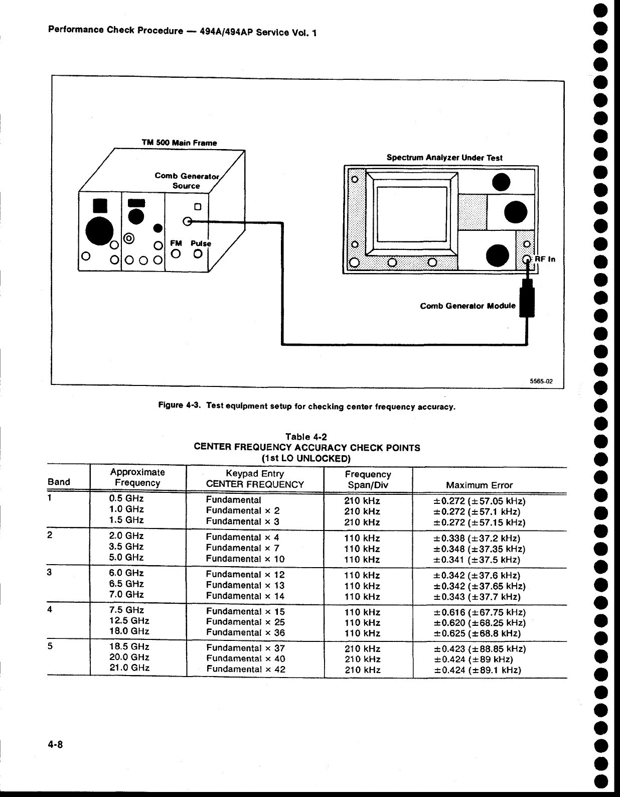
Performance
Check
procedure
- 4g4A/4g4Ap
Service
Vol.
1
TM 5OO
Main Frame
Flgure
4-3. Test
equipment
setup for
checking
center f.equency
accuracy.
Tabte
4-2
CENTER
FREOUENCY
ACCURACY
CHECK POINTS
(1sr
LO
UNLOCKED)
O
o
o
o
a
o
o
o
o
o
O
o
o
a
a
o
o
o
o
o
o
o
a
o
o
o
o
o
a
o
o
o
o
o
O
o
o
a
a
o
o
o
O
o
Band Approximate
Frequency Keypad
Entry
CENTER
FREOUENCY Frequency
Span/Div Maximum
Error
10.5 GHz
1.0
GHz
1.5
GHz
Fundamental
Fundamental x 2
Fundamental
x 3
210 kHz
210
kHz
210
kH,z
*.0.272
(*57.05 kHz)
t0.272 (*57.1 kHz)
*.4.272 (*57.15
kHz)
22.0
GHz
3.5
GHz
5.0 GHz
Fundamental
x 4
Fundamental x 7
Fundamental x 10
110 kHz
110 kHz
'110
kHz
10.338
(*.37.2kH2)
i0.348 (*37.35
kHz)
*0.341
(137.5
kHz)
36.0 GHz
0.5 GHz
7.0
GHz
Fundamental
x 12
Fundamental
x 13
Fundamental x 14
110 kHz
110
kHz
110
kHz
*.4.942 (+37.6
kHz)
*,4342
(*37.65
kHz)
:E0.343
(*37.7
kHz)
47.5
GHz
12.5
GHz
18.0
GHz
Fundamental x 15
Fundamental
x 25
Fundamental x 36
110
kHz
110
kHz
110
kHz
*0.616
(*67.75
kHz)
*0.620 (*68.25
kHz)
*0.625
(*68.8 kHz)
518.5
GHz
20.0
GHz
21.0
GHz
Fundamental x 37
Fundamental x 40
Fundamental x 42
214
kHz
210
kHz
210
kHz
*.0.423
(*88.85
kHz)
!.0.424
(+89
kHz)
*0.424
(i89.1 kHz)
4-8
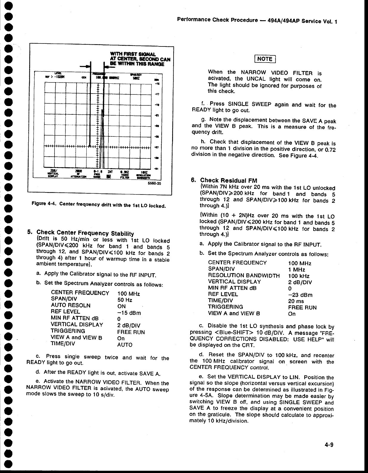
o
o
o
o
o
a
a
I
o
o
o
o
a
o
a
O
a
o
a
a
o
o
o
o
a
o
o
o
O
o
O
o
o
o
o
a
o
o
o
o
o
o
a
o
wrTlt
F|RST
stOilAL
ATC€NTER,
SEOol{D
CAil
EE Wrn$t TH|S
RAI{OE
r|
_ta
-tt
-tl
{l
-€
€
4'
{
{l
5s6035
Figure 4-4. Cenler frequency drift with the 1st LO tocked.
5. Check
Center
Frequency
Stabilitv
lplrl i.f
50
Hzlmin'or
r".J *itii-'irt Lo tocked
(SPAN/D|V<200
kHz for band 1 and bands 5
through
12, and SPAN/D|V<I0O
kHz for bands
2
through
4) after
t hour
of warmup
time
in a stable
ambient
temperature).
a. Appty
the
Catibrator
signalto
the
RF tNpUT.
b. Set the
Spectrum
Analyzer
controls
as
follows:
CENTER
FREQUENCY 1OO
MHz
SPAN/DIV S0
Hz
AUTO
RESOLN ON
REF
LEVEL -15 dBm
MIN
RF
ATTEN
dB O
VERTICAL
DTSPLAY 2
dB/Dlv
TRIGGERING FREE
RUN
V|EW
A and
V|EW
B On
TIME/DIV AUTO
READY
light
to
go
out.
d. After
the
READY
light
is out,
activate
SAVE
A.
e. Activate
the NABROW
VTDEO
FILTER.
When
the
NARROW
VIDEO
FILTER
is acivated,
the
AUTO
sweep
mode
slows
the sweep
to 10
s/div.
Performance
Check
procedure
- 4g4A/4g4Ap
Service
Vol.
1
WhCN
thE NARROW VIDEO FILTER iS
acivated,
the UNCAL light will come on.
The
light
should
be ignored
for purposes
of
this
check.
f. Press SINGLE
SWEEP
again
and wait for the
READY
light
to go out.
g. Note
the
disptacement
between
the
SAVE
A peak
and the VIEW
B peak. This is a measure
of the fre-
quency
drift.
h. check that displacement
of the vtEw B peak
is
no more
than
1 division
in the
positive
direction,
or 0.72
division
in
the
negative
direction.
See Figure
4-4.
6. Check Residuat
FM
{Witnin
7N kHz
over
20
ms
with
the
i st LO
unlocked
(SPAN/D|V>200
kHz for band
1 and bands s
through
12 and
SPANIDfV>10OkHz
for bands
2
through
4.))
{Within
(10
+ 2N)Hz over
20 ms with the 1st LO
locked
(SPAN/D|V<200
kHz
for band
1 and
bands
5
through
12 and SPAN/D|V<IO0
kHz for bands
2
through
4.)l
a. Apply
the Catibrator
signatto
the
RF
tNpUT.
b. Set
the
Spectrum
Analyzer
controls
as follows:
CENTER
FREOUENCY 100
MHz
SPAN/DIV 1 MHz
RESOLUTION
BANDWTDTH
100 kHz
VERTICAL
DTSPLAY 2
dB/DtV
MIN
RF
ATTEN
dB O
REF
LEVEL
TIME/DtV
TRIGGERING
VIEW
A and VIEW B
-23 dBm
20 ms
FREE
RUN
On
c. Disable
the 1st LO synthesis
and phase lock by
pressing <Blue-SHIFT> 10
dB/DlV. A message
"FRE-
OUENCY
CORRECTIONS
DTSABLED:
USE HELp,.wiil
be displayed
on the CBT.
cl. Reset the SPAN/DIV
to 100 kHz, and recenter
the 100
MHz calibrator signal on screen with the
CENTER
FREOUENCY
controt.
E. SEt
thE VERTICAL
DISPLAY
tO LIN. POSitiON
thE
signal so the slope (horizontal
versus
vertical
excursion)
of the response
can
be determined
as illustrated in Fig-
ure 4-5A. Slope determination may be made easier by
switching
VIEW B off, and using SINGLE
SWEEp and
SAVE
A to freeze the display
at a convenient
position
on the graticule. The slope should calculate to approxi-
mat€ly
1
0 kHzldivision.
4-9
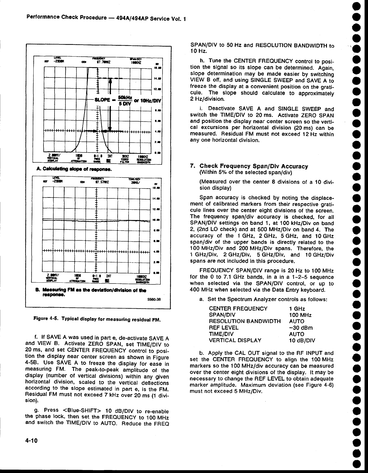
Performance
Check
procedure
- 4g4Al4g4Ap
Service
Vol.
1
cr gl.TttB lm{ iv
ra.l
ta.,
t2.a
a.l
a.a
2-a
t.l
A C.bubu|g tbp. of |lteon|..
E -2$el .a( t.5:rrq _2rS/--* n
la.a
ta.t
t:.t
ra.
a,l
a.a
{.1
2.4
a.l
.T IM
n
B. Lr.r|dog Ft .t lhc drylato||/dl'rlaloo ot urc
roapo||ac.
Figure 4-5. Typical display for measuriag residual FM.
f. lf SAVE
A was
used
in
part
e,
de-activate
SAVE A
and vtEW B. Activate
zERo spAN, set TtME/Dlv
to
20 ms, and set CENTER
FREQUENCY
controt
to posi-
tion
the display
near
center
screen
as shown
in Figure
4-58. Use SAVE
A to freeze
the display
for easl in
measuring FM. The peak-to-peak
amplitude
of the
display
(number
of vertical
divisions)
within any given
horizontal
division,
scaled to the vertical deflections
according
to the slope
estimated
in part e, is the FM.
Residual FM
must
not exceed
7 kHz
over
20
ms (1
divi_
sion).
S. Press <Blue-SHIFT>
10 dB/DlV
to re_enable
the phase
tock,
then set the FREQUENCY
to 100 MHz
and
switch
the
TIME/DIV
to AUTO.
Reduce
the FREQ
4-10
SPAN/DIV
to 50 Hz
and RESOLUTTON
BANDWIDTH
to
10 Hz.
h. Tune
the CENTER
FREQUENCY
controt
to posi-
tion the signal
so its slope
can be determined.
Again,
slope determination
rnay
be made
easier
by switching
VIEW B off, and
using
SINGLE
SWEEP and
SAVE
A to
treeze
the
display at a convenient
position
on the
grati-
cule. The slope should calculate to approximately
2 Hzldivision.
i. Deactivate
SAVE A and SINGLE
SWEEP
and
switch the TIME/DIV
to 20 ms. Activate
zERo spAN
and
position
the
display near center
screen
so
the
verti-
cal excursions
per horizontal
division
(20
ms) can be
measured.
Residual
FM
must not
exc€ed
12
Hz within
any
one horizontal
division.
7. Check Frequency Span/Div Accuracy
(Within
5%
of the selected
span/div)
(Measured
over
the
center
I divisions
of a 10
divi-
sion
display)
Span
accuracy
is checked
by noting
the displace-
ment of calibrated
markers
from their
respective
grati-
cule lines over
the center eight
divisions of the
screen.
The frequency
span/div
accuracy
is checked,
for all
SPAN/DIV settings
on
band 1, at 100
kHz/Div
on band
2, {2nd
LO check) and
at 500
MHz/Div
on band
4. The
accuracy of the 1
GHz, 2 GHz. 5 GHz, and 10 GHz
spanldiv of the upper bands is directly related
to the
100 MHz/Div
and 200
MHz/Div spans. Therefore,
the
1 GHzlDiv, 2 GHz/Div, 5
GHz/Div, and 10
GHz/Div
spans are not included
in
this
procedure.
FREOUENCY
SPAN/DIV
range
is
20 Hz
to 100
MHz
for the 0 to 7.1
GHz bands, in a in a 1-2-5 s€quence
when selected via the SPAN/DIV control, or up to
400 MHz
when selected via
the
Data
Entry keyboard.
a. Set
the
Spectrum
Analyzer controls as
follows:
CENTER
FREOUENCY 1 GHz
SPAN/DIV 100 MHz
RESOLUTIONBANDWIDTH
AUTO
REF LEVEL -30 dBm
T|ME/D|V AUTO
VERTTCAL
DTSPLAY 10
dB/DtV
b. Apply
the CAL
OUT signal to the
RF INPUT and
set the CENTER FREQUENCY
to align the 100 MHz
markers so
the 100 MHz/div accuracy
can
be
measured
over
the
center
eight
divisions
of
the
display. lt may
be
necessary
to change
the REF LEVEL to obtain
adequate
marker
amplitude.
Maximum
deviation
(see
Figure
4-6)
must
not
exceed
5 MHz/Div,
o
o
o
o
a
o
o
a
o
a
o
a
o
a
a
o
o
o
o
a
o
o
o
o
o
o
a
o
o
o
o
o
a
o
o
O
O
a
a
o
O
o
o
o
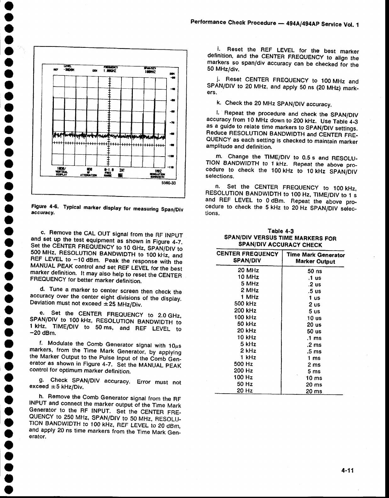
E -Otr .rr t.Eq' i5tr TI
-t
--
..4
-r
-tt
-
{
-ll
^rla
trl 'l ''t I' r'
ss603it
o
o
o
t
O
o
a
o
o
a
o
a
O
o
t
O
a
o
a
a
O
o
o
o
a
o
o
o
a
o
I
o
o
o
o
o
t
t
a
o
o
o
I
o
Performance
Check
procedure
- 4g4AJ4g4Ap
Servlce
Vol.
1
i. Reset the REF LEVEL for tho best marker
definirion,
and the CENTER
FREouENcy t" ariln ii.,e
ryt9rs so span/div
accuracy
can be checked
ilr the
50
MHz/div.
j. Reset
CENTER
FREOUENCY
to 100
MHz and
SPAN/D|V
to 20 MHz,
and
apply
50 ns (20
frlHzy
maif<-
ers.
k. check the
20
MHz
spAN/DlV
accuracy.
l. Repeat
the procedure
and check
th€ SPAN/D|V
accuracy
from
10
MHz
down
to 200
kHz. Use
faOte
q-S
as a guide
to relate
time
markers
to spAN/Dlv
settings.
Reduce
RESOLUTION
BANDWIDTH
and
CENTER
FR]E.
OUENCY
as each
setting
is
checked
to maintain
marker
amplitude
and
definition.
_ -
rn. Change
th€ T|ME/D|V
to 0.5 s and RESOLU_
TION BANDWTDTH
to 1kHz. Repeat
the above
pro_
cedure
to check the 100
kHz to 10 kHz SpANfDtV
selections.
N. SEt thE CENTER
FREQUENCY
tO 'IOO
KHZ,
RESOLUTTON
BANDWTDTH
to 100
Hz,
T|ME/DIV
to.t s
and REF LEVEL
to 0 dBm. Repeat
the above pro-
cedure
to check
the S
kHz to 20
Hz SpAN/D|V
selec_
tions,
Figure
4S. Typical
marker
dlsplay
for measuring
Span/Div
accutacy.
c. Remove
the
CAL
OUT
signat
from
the
RF
tNpUT
and
set up the
test equipment
;s shown
in Figure
4_7.
set the CENTER
FREOUENCy
to 10
eni, bnlr.rTDtv
to
500 MHz,
RESOLUTTON
BANDWIDTH
to'100
kHz,
and
REF
LEVEL
to -10 dBm. peak the response
with the
MANUAL
pEAK
controt
and
set REF
LE'EL for
the
best
marker
definition.
lt may
also
help
to reset
the
CENTER
FREQUENCY
for b€tter
marker
definition.
d. Tune
a marker
to center
screen
then
check
the
accuracy
over
the center
eight
divisions
of the display,
Deviation
must
not
exceed
*25 MHz/Div.
E. SEt thE CENTER
FREOUENCY
tO 2.0
GHZ,
SPAN/DIV
to 100
kHz, RESOLUION BANDWTDTH
to
1
If., T|ME/D|V to 50 ms, and REF LEVEL to
-20 dBm.
f. Modulate
the
Comb
Generator
signal
with
1Ops
markers,
from the Time Mark Generato-r,
by applying
the
Marker
Output
to
the
pulse
Input
of tte iomU denl
erator.as
shown
in
Figure
4-7. S;t the MANUAL
pEAK
control
tor optirnum
marker
definition.
g. . C[e9k SPAN/D|V
accuracy. Error must not
exceed
*5 kHz/Div.
h. Remove
the
Comb
Generator
signal
from
the RF
INPUT
and
connect
the
marker
output
6t the
Time
Mark
Generator
to the RF tNpUT. Sei tne CENTER
FRE-
OIENCY
to 2s0
MHz,
SpAN/D|V
to 50
MHz,
RESOLU-
NON
BANDWIDTH
to 1oo kHz,
REF
LEVEL
to 20
dBm,
and
apply
20
ns
time
markers
from
the
Time
Mark
Gen_
erator.
Tabte
4-3
SPAN/DrV
VERSUS
T|ME
MARKERS
FOR
SPANiD|V
ACCURACY
CHECK
CENTER
FREQUENCY
sPAN/DrV Tlme
Mark
Generator
Marker
Output
20
MHz
10 MHz
5
MHz
2 MHz
1 MHz
500
kHz
200
kHz
100
kHz
50 kHz
20
kHz
10
kHz
5 kHz
2kHz
1 kHz
500 Hz
200 Hz
100 Hz
50 Hz
50
ns
.1
us
.2
us
.5
us
1us
2us
5us
10
us
20
us
50 us
.1 ms
.2 ms
.5 ms
1ms
2ms
5ms
10
ms
20
ms
Hz
4-11
Perlormance
Check
procedure
_ 4g4A/494Ap
Service
Vol.
1
8. Check Marker Accuracy
Accuracy
with
the
1st
LO untocked
is * {(20%
of the
Span/Div
or Resolution
Bandwidth,
whichever
is
greater)
+ (CF x Reference
Frequency
Enor)
* 15N
kHzl.
Accuracy
with 1st LO tocked
is * ((20%
of the
Span/Div
or Resolution
Bandwidth,
whichever
is
greater).+
(CF x gglsr.nce Frequency
Error)
+ (2N
+ 25)Hz).
(A
marker
accuracy
is 1% of the
measured
span)
The 1st LO is not phas€-locked
in Fre_
quency
Span/Div
settings
>200 kHz. For
Span/Div
settings (200kH2, the lst LO
may be unlocked by first going to an
unlocked
Span/Div
setting
and
disabling
fre_
quency corr€ctions (Btue_SHtFT
1O
dB),
then
-spanning
down to a Span/Div
settint
(200 kHz.
Quantity
N is the lst LO harmonic
number
used
for the first conversion.
press HELp
and <Blue-SHIFT>
BANDV
for the value
of
N.
(3) Disable frequency corrections by pressing
<Blue-SHIFT>
1
0dB/DlV.
(4) R_€set
the spAN/Dtv to 100
kHz white
keeping
the 600 MHz harmonic
of the calibrator
signal
neai
center'screen
with the CENTER/MARKER
FRE_
OUENCY control.
The 1st
LO is now
unlocked.
(5) Enable a single marker,
and position
it on the
signalby
pressing
<Green-SHIFT>
PEAK
F|ND.
(6) Check
that
the marker
readout
is within
35
kHz
of the center
frequency
readout.
(7') Press <Blue-SHtFT> 1OdB/DtV
to enabte
phaselock.
(8) Use the CENTER/MARKER
FREQUENCY
con-
trol to reposition the calibrator harmonic near
center-screen.
(9) Press <Green-SHIFT>
PEAK
F|ND
to position
the
marker
on
the signal.
(10) Check that the marker frequency
readout
is
within 47
kHz of the
center
frequency
readout.
The
factor
(CF x Reference
Frequency
Error) is canceled
when
ihe
CAL
OUT signat
is
used.
b. Check
A marker
accuracy.
(1) Set
the
Spectrum Analyzer
controls
as follows:
o
o
o
o
a
a
o
o
o
a
o
a
o
a
a
o
o
a
o
a
o
o
o
o
O
o
o
o
O
o
o
o
a
o
a
o
I
o
a
o
o
o
O
o
CENTER
FREQUENCY
sPAN/DtV
AUTO
RESOLN
REF
LEVEL
VERTICAL
DISPLAY
TtME/DtV
TRIGGERING
0-60
GHz
100
MHz
On
-20 dBm
10
dB/Drv
AUTO
FREE
RUN
a. Check slngle
marker
accuracy.
(1)
Apply
the
CAL
OUT
signatto
the
RF
tNpUT.
(2) Set
the Spectrum
Analyzer
controls
as follows:
CENTER
FREOUENCY
sPAN/DlV
AUTO
RESOLN
REF
LEVEL
VERTICAL
DISPLAY
TrME/DtV
TRlGGERING
600
MHz
500
kHz
On
-20 dBm
10
dB/Dtv
AUTO
FREE
RUN
(2) Enable
A markers
by
pressing
<Green-SHIFT>
A MKR, and tune one marker
to a harmonic
of the
calibrator signal. Press <Green-SHIFT>
MKR 1*MKR 2, and tune the second marker
to
another harmonic
of the
catibrator
signal.
(3) Check
that the A marker
frequency
readout
is
within
17o of
the
measured span.
4-12
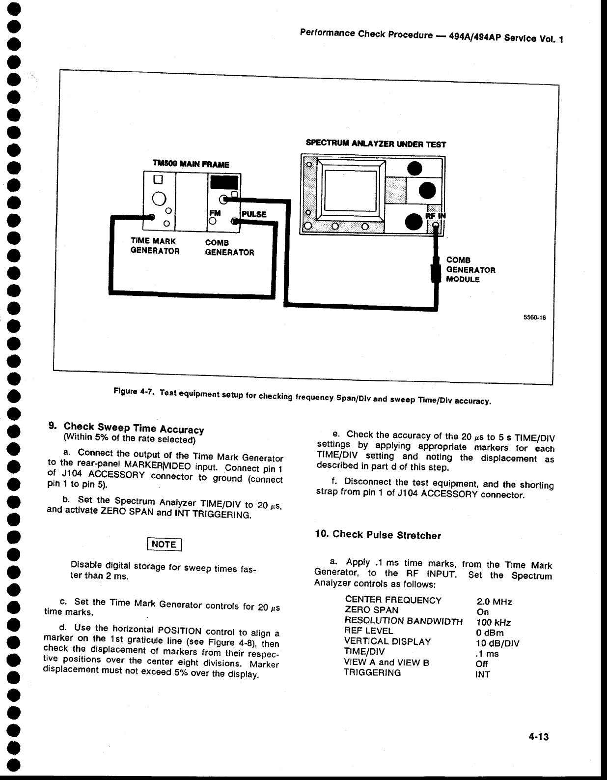
o
o
a
o
o
o
a
o
o
I
I
t
o
a
a
o
a
o
o
o
a
I
o
O
o
o
t
o
I
O
t
a
o
a
a
O
O
I
O
o
o
o
o
o
Performanee
Check
procedure
_ 4g4Al4g4Ap
Servlce
Vol. 1
SPECTRIfr AI{I.AYZER
UI{OER
TEST
coME
OENERATOR
MOOULE
Figure
4-7' Test equipment setup for checklng frequency span/Dlv and sweep Time/Div accuracy.
9. ^C.*:*_qyegp
Time
Accuracy
(Within
S%
of
the
rate
serecitJi'
a. Connect
the output
of the Time
Mark
Generator
to the
rear-panet
MARKERI/|DEO
input.--6'onnect
pin
1
of J104 ACCESSORY
connector
ti-groiio (connect
pin
1
to pin
S).
- .b. _Set
the Spectrum
Analyzer
TIME/D|V
to 20 ps,
and
activate
zERo SpAN
ano
tNT
rireb-lnjr.rc.
Disable
digital
storage
for sweep
times
fas-
t€r
than
2 ms.
c. Set the Time
Mark
Generator
controls
for 20
ps
time
marks.
d. use the horizontal
poslTloN controt
to align
a
marker..on
rhe
1st graticute
tine
(see
Fd;; 4-B),
then
check
the displacement
of markers
trori-ineir
respec-
tive positions
over
the c€nter
eight
divisions.
Marker
dispfacement
must
not
exceed
S/o
over
the
display.
e. check
the
accuracy
of the
20
ps
to 5 s TIME/D|V
::l!'!.S_r by apptying appropriate
markers ,or each
TIME/DlV
setting and noting the displac€ment
as
described
in
part
d of this
step.
f. Disconnect
the-test_equipment,
and the shorting
strap
from
pin
1 of Jl04 ACCESSORy
connector.
10.
Check Pulse Stretcher
a. Apply
.1 ms time marks,
Generator, to the RF lNpUT.
Analyzer
controls
as
follows:
CENTER
FBEOUENCY
ZERO
SPAN
RESOLUTTON
BANDWIDTH
REF
LEVEL
VERTICAL
DISPLAY
TtME/DtV
VIEW
A and
VIEW
B
TRIGGERING
from
Setthe Time Mark
the spectrum
2.0 MHz
On
100
kHz
0 dBm
10
dB/Dtv
.1 ms
off
INT
4-13
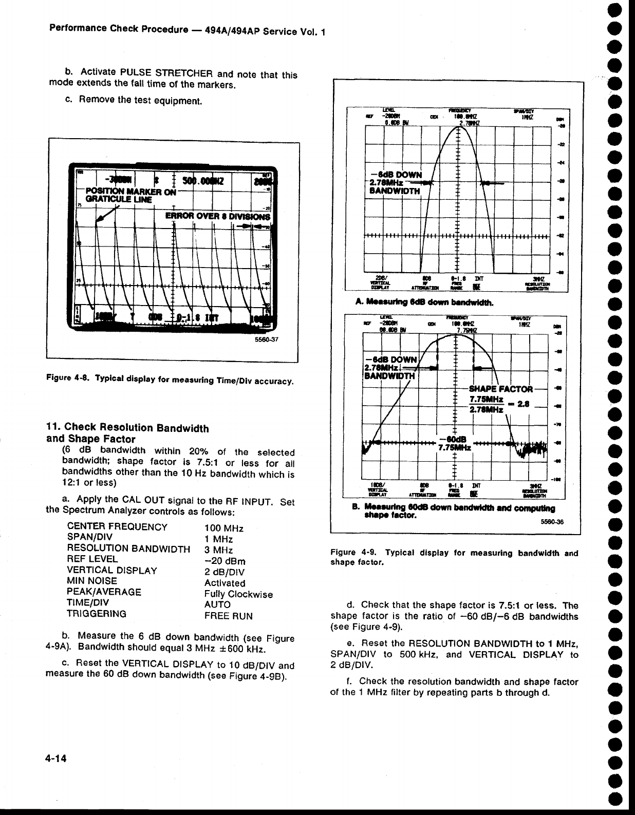
Performance
Check
procedure
- 4g4A/4g4Ap
Service
Vol.
1
b. Activate
PULSE
STRETCHER
and
nore
that this
mode
extends
the talt
time
of the
markers.
c. Remove
the
test
equipment.
o
o
o
o
I
o
)
o
o
o
a
a
o
a
o
a
t
o
o
o
o
o
a
o
O
o
o
o
o
a
o
O
a
o
o
O
o
o
a
o
I
o
I
o
Figure 4€. Typlcal display for measuring Time/Div accuracy.
11.
Check
Resolution
Bandwidth
and
shape Factor
(6 dB bandwidth within 2ov" of the s€lected
bandwidth;
shape factor is 7.S:l or less lor all
bandwidths
other
than
the 1O
Hz
bandwidth
which is
12:1
or less)
a. Apply the
CAL
OUT
signat
to
the
RF lNpUT.
Set
the
Spectrum
Analyzer
controls
as
follows:
CENTER
FREQUENCY
sPAN/DrV
RESOLUTION
BANDWIDTH
REF LEVEL
VERTICAL
DISPLAY
MIN
NO]SE
PEAK/AVERAGE
TrME/DrV
TRIGGERING
b, Measure
the
6 dB down
bandwidth
(see
Figure
4-9A).
Bandwidth
shoutd
equal3
MHz
*600 kHz.
c. Reset
the vERTtcAL
DtspLAy
to 10
dB/Dtv
and
measure
the 60
dB
down
bandwidth
(see
Figure
4_gB),
Figure 4-9. Typical display for measuring
bandwldth
and
shape factor.
d. Check
that the shape factor is 7.5:1
or less. The
shape factor is the ratio of -60 dB/-6 dB bandwidths
{see
Figure
4-9).
e. Reset
the RESOLUTION
BANDWIDTH
to 1 MHz,
SPAN/DIV to 500
kHz, and VERTICAL DISPLAY to
2 dB/DrV.
f. Check the resolution
bandwidth and shape factor
of the 't MHz filter by repeating
parts b through d.
100
MHz
1 MHz
3 MHz
-20 dBm
2 dBlDtv
Activated
Fully
Clockwise
AUTO
FREE
RUN
ltl
-8dBDOWN 1
EANDW|OTH /
\
r
ItI
\
E -z!il nl
€
.a
{a
t
{
{
.,aa
{
{
t-l.t DaT
gE
A" t rt||rhg tG doun b.nffdtt|.
-0d8DowN
)?illt;l-
BAIIDWIDTH
I tl I t\ | |
S}IAPE
FACTOR
*ffi-"t
lt\r I
II+l
t+l
*r--zffrr*
t*l V
E -znl .E tt.atc
D
r
TI
.it
{
<
-
-
-l
{
-
-t-
Fr.t Dfi
&E
a. llolrtqlnq COdA
dorn DenrMrt0r
end computhg
d'|Pc tactot 556{r..6
4-14
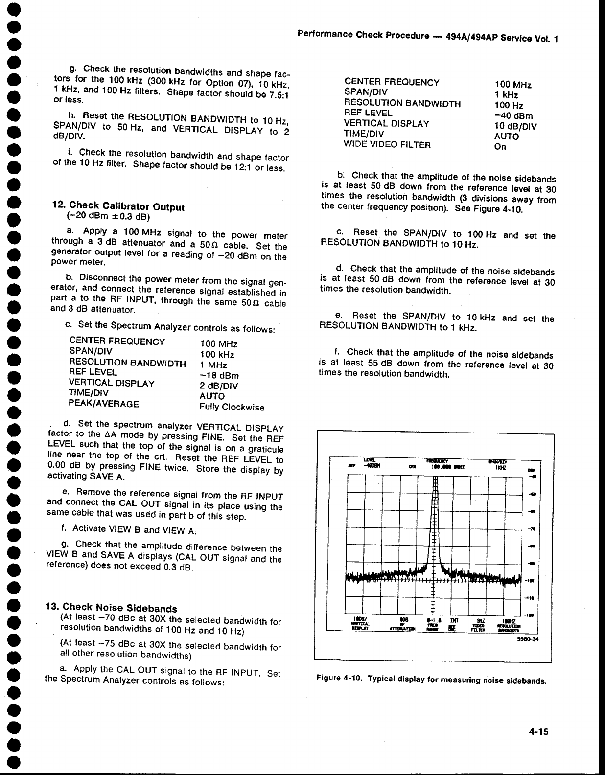
I
o
o
t
o
t
o
I
o
o
I
I
o
a
a
a
a
O
a
a
o
o
o
o
a
o
o
a
a
I
a
o
I
o
o
o
o
I
O
o
I
o
I
o
Perlormance
Check
procedure
_ 4g4Ll4g4Ap
Servlce
Vot.
1
g. Check
the
resolution
bandwidths
and
shape
fac_
tors for the 100
kHz (300ftHa
for Option
bA, 10
kHz,
1
kHz,
and
100
Hz
fitters.
Shape
factlistroufd
be
7.5:1
or
less.
h. RESET
thE
RESOLUTION
BANDWIDTH
tO
'IO
HZ,
qlglptv to 50 Hz,
and
VERlCnl.'drdpr-ry
ro 2
dB/Dlv.
i. Check
the resolution
bandwidth
and
shape
factor
of the 10
Hz
fitter. Shape
factor
should
i" iZrt or tess.
12.
Check
Catibrator
Output
(-20
dBm
*0.3 dB)
Apply
a 100
MHz signal
to the power meter
through
a 3 dB attenuator
anO
a SOO
"d;t". Set the
generator
output
level
for a reading
of _20 dBm
on the
power
meter.
b. Disconnect
the power
meter
from
the signal
gen_
erator,
and
connect
the
reference
signat
established
in
part
a to the
RF tNpUT,
through
thd same
50O cable
and
3 dB attenuator.
c. Set
the
Spectrum
Analyzer
controls
as
follows:
b. Check
that
the amplitude
of th€
noise
sidebands
is at least
50 dB down
from the reference
lev€l
at g0
times the resolution
bandwidth
(3 divisions
away
from
the center
frequency
position).
See Figure
4-10.
c. Reset the spAN/Dlv to 1oo
Hz and set the
RESOLUTTON
BANDWTDTH
to 10
Hz.
d. check that
the
amplitude
of the noise
sidebands
is at least 50
dB down from the reference
level
at 30
times
the resolution
bandwidth.
€. Reset
the spAN/Dtv to 10 kHz and set the
RESOLUTION
BANDWIDTH
to 1
kHz.
f. Check
that
the amplitude
of the noise
sidebands
is at least
55 dB down
from the reference
level
at O0
times
the resolution
bandwidth.
CENTER
FREOUENCY
sPAN/DtV
RESOLUTION
BANDWTDTH
REF
LEVEL
VERTICAL
DISPLAY
TrME/DtV
WIDE
VIDEO
FTLTER
100
MHz
1
kHz
100
Hz
-40 dBm
10
dB/Dtv
AUTO
On
CENTER
FREQUENCY
SPAN/DIV
RESOLUTION
BANDWIDTH
REF
LEVEL
VERTICAL
DISPLAY
TfME/Dlv
PEAK/AVERAGE
100
MHz
100
kHz
1
MHz
-18
dBm
2 dBlDtv
AUTO
Fully
Clockwise
; .d. .Sel
the spectrum
analyzer
VERTICAL
DlSpLAy
factor
to th€ AA mode
by pressing
firuE.-'Set
the REF
LEVEL
such
that
the
top'oi the
siinat
is'on
a graticute
line
near
the top of the crt. nesJt ttre
neF LEVEL
to
0.99
gP by pressing
F|NE
twice. Store
ttre
display
by
activating
SAVE
A.
_e.
Remove
the
reference
signaf
frorn
the
nF tNpUT
and
connect
the CAL
OU.T
signll in its place
using
the
same
cable
that
was
used
in
part
b
of
this
step.
f. Activate
VIEW
B and
VIEW
A.
g. Check
that
the
amplitude
difference
between
the
VIEW
B and
SAVE
A disptays
(CAL
OUi iignar
anO
the
reference)
does
not
exceed
b.S'Og.
13.
Check
Noise
Sidebands
(At
least
-70 dBc
at
30X
the
selected
bandwidth
for
, resolution
bandwidths
of
100
Hz
and
10
Hz)
(At
least
-75 dBc
at
gOX
the
selected
bandwidth
for
all
other
resolulion
bandwidths)
1. Appty
the
CAL
OUT
signat
to
the RF
tNpUT.
Set
the
Spectrum
Analyzer
controls
as
follows: Figure 4-10. Typical disptay
for measuring noas€
sidebands.
E -St cd ra.C rttr - |rq n
{
{
-
_tt
-
-
-rl
-il4
-tt
t ll{l
r
I
rrl(\l4ftr I
556034
4-15
Performance
Check
procedure
_ 4g4Al4g4Ap
Service
Vol.
1
14.
Check
Frequency
Response
(Response,
about the midpoint
between
two
€xtremes,
measured
with
10
dB of RF
attenuation
and peaking
optimized
in the applicabl€
bands
for
each
center
frequency
setting,
is as
follows:
Band
1: +1.5
dB
from
10
kHz
to 1.g
GHz
Band
2:
*2.5 dB
from
1.7
to S.5
GHz
Band
3: r2.S dB from
3 to
7.1
GHz
Band
4: i3.S dB
from
5.4
to 1g
GHz
Band
5: iS.O
dB
from
t5 to 21
GHz)
(Response
with
respect
to 100 MHz
is
as,ollows:
Band
1:
*2.5 dB
from
t0 kHz
to 1.g
GHz
Band
2: *3.5 dB
from
t.Z to 5.5
GHz
Band
3: *3.5 dB
from
3 to 7.1
GHz
Band
4: *4.5 dB
from
5.4
to 1g
GHz
Band
5: *6.5 dB from
t5 to 21
GHz)
. The response
at each check point,
above
band l,
should
be
peaked
with
the
MANUAL
PEAK
controt.
^, ?: Check frequency
response
from 0.01
GHz to
21
GHz
(Bands
1 through
5).
(1) Connect
the CAL OUT
signat
to the
RF tNpUT,
and perforrn
the <Blue-SHIFT>
CAL
routine.
(2) Set
the
Spectrum
Analyzer
controls
as
follows:
CENTER
FREQUENCY 1OO
MHz
SPAN/D|V 500
kHz
RESOLUTION 3 MHz
REF
LEVEL -20 dBm
VERTICAL
DTSPLAY 2 dB/Dtv
MIN
RF
ATTEN
dB O
TIME/DIV AUTO
00) D€activate
MAX HOLD,
and repeat parts 6
through
10
for
a CENTER
FREQUENCy
of 1.5
GHz
(1
GHz
to 1.8
GHz).
(1
1) Calculate
the hatfway point between the
highest
and the lowest peak from the peak data
noted
in
parts
g and
10.
(12) Check
that swept
frequency
flatness
is within
11.5
dB in Band
1.
(13) Switch the Spectrum
Analyzer to Band 2
(<Blue-SHIFT>
BANDA),
CENTER
FREeUENCy
to
2.7 GHz,
and
SPAN/DIV
to 200
MHz.
(14) Reset the sweep oscillator controls for a
sweep
output
trom 1.7
GHz-3.7 GHz. Enable
sin-
gle
sweep
on
the
sweep
oscillator.
Before sweeping
any range in Bands 2
through
5, set
th€
CENTER
FREQUENCy
to
the center
of the
range;
apply
a cw signal
at
this center frequency; and peak the
response
with
the
MANUAL
PEAK
control.
(15) Check that amptitude
deviation from thE
'1
00
MHz
reference
does
not
exceed f3.5 dB.
(16) Again,
make
a note
of the highest
and
lowest
peaks
for later
comparison.
(17)- Check frequency response in the range
3.7
GHz-5.5 GHz (CENTER FREQUENCY Lt
4.6
GHz and SPAN/D|V
at 200
MHz). Continue
making
notes
of the highest
and lowest
peaks
for
comparison
later
on.
(18) Check
Bands
3 through
5 according
to Tabte
44. 8e sure to make a note of the highest
and
lowest
peaks
after each
check.
(19) Calculate the halfway point between the
highest and the lowest peak from the peak data
noted in
parts
16 and17.
(20) Check
that swept frequency
flatness
is within
*2.5 dB in Band
2 and
Band
3, within
*3.5 dB in
Band 4,
and
within *5.0 clB in
Band
5.
lf any
segment
or portion
of the span
fails
to meet the specification,
set the FRE-
QUENCY
to the center
of this
portion;
apply
a cw marker
at this center
frequency
and
re-peak
with
the MANUAL
or AUTO
PEAK-
lNG.
Decrease
the
FREQUENCY
SPAN/D|V
to display
that
portion
and
then recheck
the
frequency
response for
this
portion.
PEAK/AVERAGE Fully
Counterclockwise
o
o
o
o
a
o
a
I
o
a
a
o
o
o
o
o
o
o
o
o
o
t
o
o
o
o
o
o
o
o
o
o
a
o
o
O
o
o
a
o
o
a
o
o
(3) Set
the
CAL AMPL
adjustment
for
5 divisions
on
the Spectrum
Analyzer
diiptay. This
is
the
1OO MHz
reference. Activate
SAVE
A to save
the reference.
(4) Connect
th€ test equipment
as shown
in Figure
4-11.
(5) Set
the
sweep
oscillator
controls
for
a cw
output
that rnatches
the SAVE
A display
(output
frequency
of 100
MHz and an output amptituOi
of approxi-
mately
-20 dBm).
(6) Deactivate
SAVE
A. Reset the CENTER
FRE-
QUENCY
to 500
MHz, and SpANiDtv
to 100
MHz,
and
activate
MAX
HOLD.
(/) R:seJ
the sweep
oscillator
controls
for a sweep
output from 0.01
GHz-1 GHz. Enable singlb
sweep
on
the sweep
oscillator.
(8) Check that amplitude deviation from the
100
MHz reference
does
not
exceed
*2.S dB.
(9) Make
a note
of the highest
and
lowest
peaks
for
later
comparison.
4-16
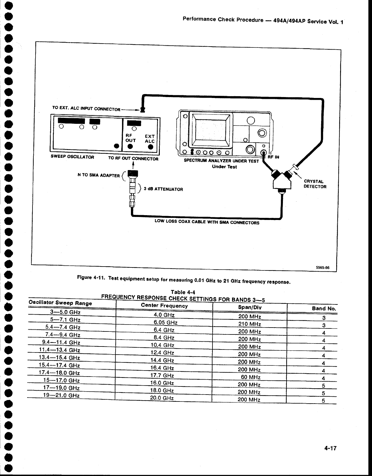
Perforrnance
Check procedure _ 4g4Ll4g4Ap Servlce Vol. 1
4-17
o
o
o
o
o
a
o
I
o
o
a
o
o
a
a
I
o
I
o
o
o
a
o
o
t
o
J
a
t
t
O
a
I
o
a
o
o
o
o
a
a
o
I
o
Oscillator Sweep Range
3-5.0 GHz
5-7.1 GHz
5.4-7.4 GHz
7.4-9,4 c
70 EXT. ALC III'PUT CO{IINECTOB-
F' IoIo
RF €XT
OUT ALC
oo
o
swEEp
oSctLLATOR TO
RF
OtrT
CoxnecG SPECTRUII
AilALYZER UNDER
TEST
Undor Test
I
N ro sMA
ooaeten
fCRYSTAL
DETECTOR
) 3 dB ATTENUATOR
Low
Loss
coAx
cABLE
wrrx sul courEEroid
Figurc
4-11' Test
equipment
setup
for measuring
0.01
GHz
to 2r GHz
frequency,esponse.
Table 4-4
10.4
GHz
12.4
GHz
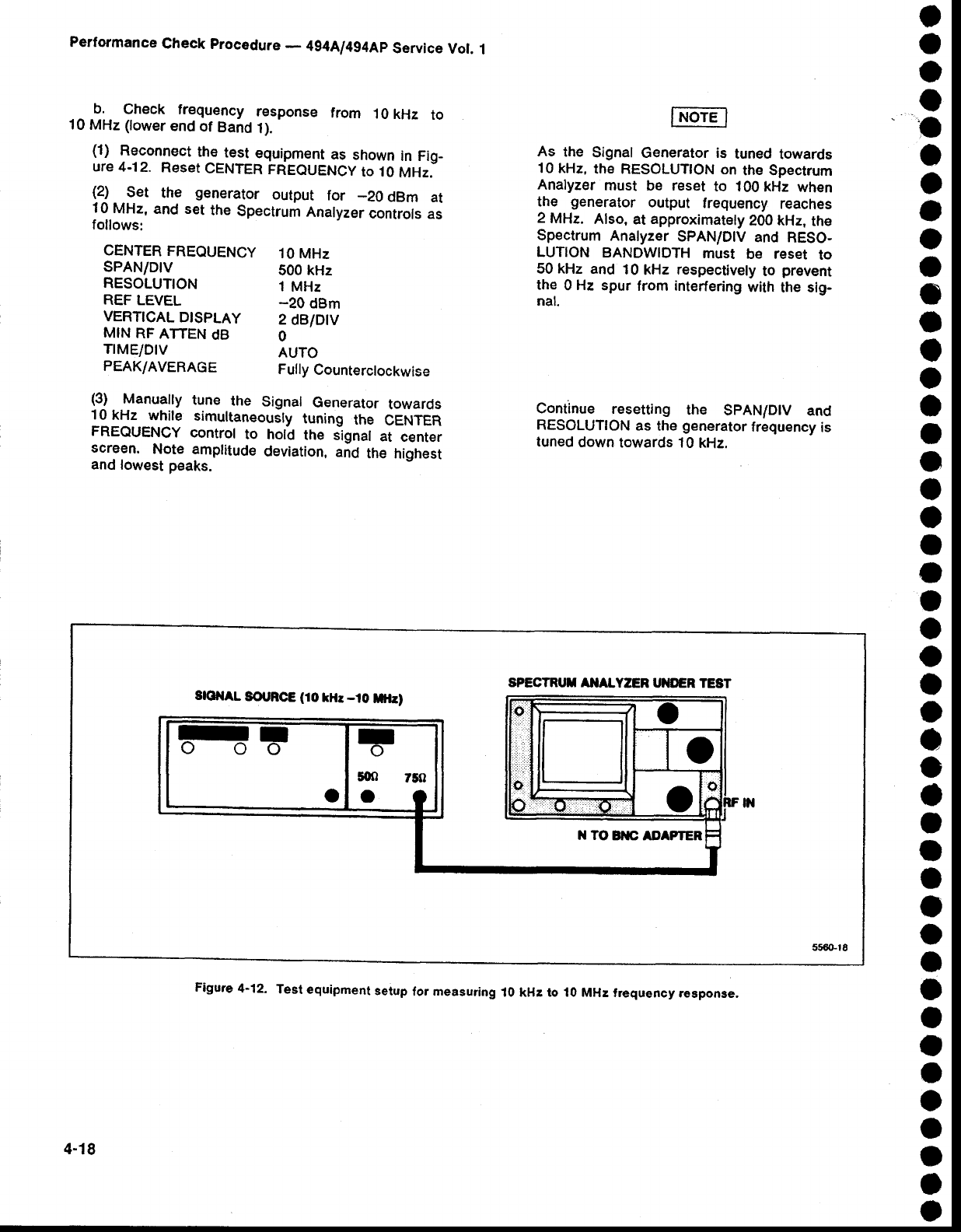
Performance
Check
procedure
- 4g4A/494Ap
Service
Vol.
1
^ b: Check frequency response from 10
kHz to
10
MHz
(lower
end
of
Band
1).
-
(1) Reconnect
the_test
eguipment
as shown
in Fig-
ure
4.12. Reset
CENTER
FREQUENCY
Io 10
MHz.
(2) Set the generator output for _20
dBm at
10
MHz,
and set
the
Spectrum
Analyzer
controls
as
follows:
CENTER
FREQUENCY 10
MHz
SPAN/DIV 500 kHz
RESOLUTION 1
MHz
REF
LEVEL -20 dBm
VERT|CAL
DTSPLAY 2 dBlDlV
MIN
RF
AfiEN dB O
TIME/DIV AUTO
PEAK/AVERAGE Fully
Counterclockwise
As the Signal
Generator is tuned
towards
10 kHz,
the RESOLUTTON
on the Spectrum
Analyzer
must be reset to 100
kHz when
the generator output frequency
reaches
2 MHa Also,
at approximatety
200 kHz,
the
Spectrum
Analyzer
SPAN/DIV
and RESO-
LUTION BANDWIDTH
must be reset to
50 kHz and 10
kHz respectively
to prevent
the 0 Hz spur
from interfering
with
the sig-
nal.
Continue resetting the SpAN/DlV and
RESOLUTION
as the
generator
frequency
is
luned
down
towards 10
kHz.
o
o
o
o
a
o
o
I
o
a
o
a
o
o
O
a
o
a
o
O
o
I
a
o
o
o
a
a
a
I
a
I
o
o
o
o
a
a
o
o
o
o
o
a
(3) Manually
tune the Signal Generator
towards
10kHz while simultaneousty
tuning
the CENTER
FREQUENCY
control to hold the signal
at center
screen. Note amplitude
deviation,
and the highest
and
lowest peaks.
SPECTRT'T
AIIALYZER
UIIDER TEST
SlOllAL SOT
RC€
(10 kltr -.t0 lrtltr)
Figure
4-12. Test
equipment
setup
for
measuring
10 kHz to 10
MHz frequency
response,
4-18
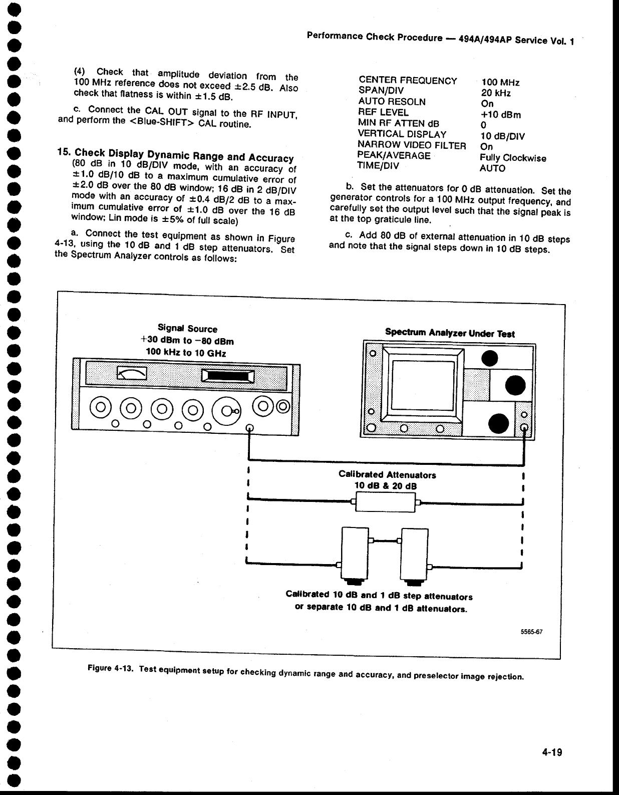
t
I
a
o
o
o
o
o
o
o
t
a
o
o
o
a
o
a
a
a
o
a
o
o
a
I
a
o
o
o
o
o
o
o
o
I
t
I
o
O
a
a
I
t
Performance
Check
procedure
_ 4g4Ll4g4Ap
Servlce
Vol.
1
(4) Check that amplitude deviation from the
100
MHz
reference_does
not,*.""J-*i.s dB. Atso
check
that
flatn€ss
is
within
*1.5 dB.
c. Connect
the
CAL.OUT
signat
to the
RF
tNpUT,
and
perform
the <Btue-SHIFT>
CAf-
iouiin".
15.,Chec_k
Display
DVnamic
Range
and Accuracy
(99
jB._il _10
dB/DtV moOe,-wirr
in-accuracy or
:!1.0 dB/l0 dB to^-a
maximum
cumulative
error
of
*2.0 dB over
the
g0
dB window;
rO
Oe-in
2 dBlDtV
rnode
wfth
an accuracy
of *0.4 ABpia to a max_
imum
cumulative
enor of *1.0 Oe'ovei
the
16
dB
window;
Lin
mode
is 15% ot fuff
ica[l-'
a. Connect
the
test equipment
as shown
in Figure
4-13-,
using
the
lOdB and
1'dB
siep"ti"nrutorr. S"t
the
Spectrum
Analyzer
controls
as foilows:
b. Set
the attenuators
for O dB attenuation.
Set
the
generator
controls
for a.
100
MHz
output
frequency,
and
carefully
set
the output
level
such
ttrai
tne
signat peak
is
at the
top graticule
tine.
c. Add 80
dB of external
attenuation
in 10
dB steps
and
note
that
th€
signal
st€ps
down
in 10
dB steps.
CENTER
FREQUENCY
sPAN/DtV
AUTO
RESOLN
REF
LEVEL
MIN
RF
ATTEN
dB
VERTICAL
DTSPLAY
NARROW
VIDEO
FILTER
PEAK/AVERAGE
TrME/DtV
100
MHz
20 kHz
On
*10
dBm
0
10
dB/DtV
On
Fully
Clockwise
AUTO
Signaf Source
*30 dBm to -80 dBm
100
kHz
to 10
GHz
Specfrum
Analyzer
Under
Ted
Calibraled Altenuators
10dB&20d8
Calfbrated 1O
dB and 1 dB step ailenuators
or separate
10 dB and i dB attenualors.
Figure
4-13' Test eguipment s€tup for checking dynamic range and accuracy, and preserecror
image fejection.
4,19
Performance
Check
procedure
- 494A/4g4Ap
Service
Vol.
1
d. Check that the signal steps down in 10
dB
(r1.0 dB) steps as attenuation
is added. Maximum
cumulative
error should not exceed 2.0
dB over the
80
dB range.
e. Deactivate
the NARROW
VTDEO
F|LTER,
return
the
external
attenuation
to 0 dB, and
change
the VERTI-
CAL
OISPLAY
to 2 dB/DlV. Set the
signat
peak
at the
reference
(top) graticule
line,
with the generator
output
control.
f. Add 16
dB of external
attenuation
in 2 dB steps,
and
note
that
the
display
steps
down
in
2 dB steps.
g, Check the display accuracy
as attenuation
is
added. Error
should
not exceed
+6.+ aep dB step,
or
exce€d
a cumulative
error
of +1.0
dB over
the i6 dB
window.
h. Return
the external
attenuation
to 0 dB. change
the VERTTCAL
DlSpLAy
to LtN. Set the
signal genera-
tor output
for a full
screen
display.
i. Check that the signal amplitude
decreases
ro
within
*0.4 divisions
of half
screen
as 6 dB of external
attenuation
is
added.
j. Check
that the signal
amplitude
decreases
ro
within
i0.4 divisions
ot 114
screen
or hatf
the
previous
amplitude
as an
additional6
dB
of
att€nuation
is
added.
k. Check that the signal amplitude
decreases
to
within *0.4 divisions
ot 1lg screen
or half the last
amplitude
as an
additional
6 dB of attenuation
is added
(for
a total of 18
dB).
t. Return
ths
vERTtcAL
DtspLAy
to 1o
dB/Dtv
and
disconnect
ths generator
from
the RF
lNpUT.
16.
Check Preseleclor Ultimate
Rejection
This
is a check
of preselector
opeiation,
not
a per_
formance
requirement
specification.
a. Connect
the test equipment
as shown
in Figure
4-13,
omitting
the step attenuators.
Set the Spect-rum
Analyzer
controls
as
follows:
CENTER FREOUENCY 3.S
GHz (Band
2)
SPAN/D|V 10
kHz
AUTO
RESOLN On
REF
LEVEL 0 dBm
VERT|CAL
DTSPLAY 10
dB/Dtv
MIN
RF ATTEN
dB O
WIDE
VIDEO
FTLTER On
T|MEIDIV AUTO
b. Set the generator
controls
for a full screen
display
output
at 3.S
GHz. peak
the response
with
the
MANUAL
PEAK
controt
or
pEAK
MENU
mode.
_ c. Change
the FREQ
RANGE
to band
3 (3.0_7.1
GHz).
d. Check
that spurious signals
are at least
too dB
down from
the level
established
in part
b. Spurious
sig-
nals above
100
dB down
from
the reference
estabtished
in part b indicate
that the ylG-tuned
preselector
filter
could
be defective.
o
o
O
o
a
o
o
o
o
a
I
o
o
o
a
o
t
O
o
o
o
t
o
o
o
o
a
o
o
o
I
t
o
o
a
o
I
a
a
o
o
o
o
o
17.
Check RF
Attenuator
Accuracy
(Within
0.5
dB/10
dB
to a maximum
of 1 dB over
the
60 dB range
from dc to 1.8
GHz; within
1.5
dB/tO
dB to a maximum
of 3 dB over the 60 dB range
from 1.8
GHz
to 18
GHz; and
within
g
dB/10
dB
to a
maximum
of 6 dB over the 60 dB range
from 1g
GHz to 21
GHz)
This is a three part procedure. part I
checks
the first
30
dB (0-30 dB) range
of
the
rf attenuator,
Part
ll checks
the remain-
ing 30 dB (30
dB-60 dB) range for fre-
quencies
up
to 18 GHz, and
part
lll checks
the
50 dB to 60 dB step
of the RF Attenua-
tor
lor frequencies
above
18
GHz.
PART I
a. Connect
the
test equipm€nt
as shown in Figure
4-14. Set
the
Spectrum Analyzer
controls
as follows:
CENTER
FREOUENCY
SPAN/DIV
RESOLUNON
BANDWIDTH
REF LEVEL
MIN RF ATTEN
dB
MIN
NOISE
PEAK/AVERAGE
VIEW
A and VIEW
B
Test
Freguency
200 kHz
100 kHz
-30 dBm
o
On
Fully
Clockwise
On
VERTfCAL
DISPLAY 2 dBlDtV
NARROW
VIDEO
FILTER On
T|ME/D|V AUTO
b. Set the power meter controls as follows:
Mode Watts
Range
Hold Out
Power
Reference Out
4-20
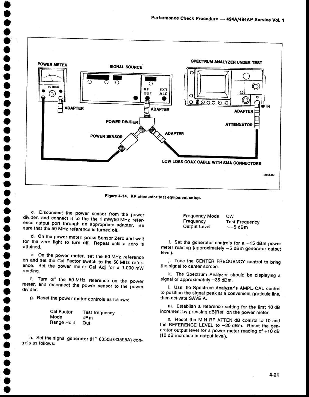
t
o
a
o
I
o
o
I
a
a
o
o
a
O
I
I
I
a
O
o
o
o
o
o
a
O
a
o
I
I
o
O
O
o
t
o
o
o
o
I
o
o
a
I
Cal Factor Test
frequency
Mode dBm
Range
Hotd Out
.h. setthe
signat gen€rator
(Hp
g3508/s3595A)
con-
trols
as follows:
Performance
Check
procedure
- 4g4Al4g4Ap
Servlce
Vol.
1
Frequency
Mode CW
Frequency Test
Frequency
Output
Level --5 dBm
i. Set
the
generator
controls
for a -15 dBm
power
meter
reading
(approximately
-5 dBm
generator
output
Ievel).
j. Tune
the CENTER
FREQUENCY
controt
to brino
the signal
to
center
screen.
k. The Spectrum
Analyzer
should
be displaying
a
signal
of approximately
-35 dBm.
l. Use
the
Spectrum
Analyze/s
AMPL
CAL
control
to position
the signal
peak
at
a convenient graticule
line,
then activate
SAVE A.
m. Establish
a reference
setting
for the first
10
dB
incrernent
by
pressing
dB[Ref on
the
power
meter.
n. Reset
the MIN
RF
ATTEN
dB control
to 10
and
the REFERENCE
LEVEL
to -20 dBm. Reset
the gen-
erator
output
level
for a power
meter
reading
of +1
0 dB
(1
0 dB
increase
in output
level).
c. Disconnect
the power sensor
from the power
divider,
and connect
it to th€ the I ,WISO
MHz refer-
ence output
port through
an appropriate
adapter. Be
sure
that
the
50 MHz
reference
is'tumed
off.
- d. On
the
power
meter,
press
Sensor
Zero
and
wait
for the-zero
light
to turn off. Repeat
until
a zero is
attained.
e. .On
the power meter,
set the 50 MHz reference
on and set the Cal Factor
switch
to the 50 MHz refer-
ence..
Set the power meter Cal Adj for a 1.000
mW
reading.
f. Turn off the 50
MHz reference
on the power
meter,
and reconnect
th€ power sensor
to th€ power
divider.
g. Reset
the
power
meter
controls
as
follows:
POWER
METER SPECTRUII
ANALYZER
UI{DER
TEST
SIGI{AL
SOURCE
ADAPTER ADAPTER ADAPTER
ATTET'IUATOf,
FOWER
DIVTDER
POTYER
SENSOR AOAPTER
LOW
LOSS
COAX
CABLE
IYITH
SMA
COI{NECTORS
RF ExT
OUT ALc
Flgure
4-14. RF
attenuator
test
equipment
selup.
4-21
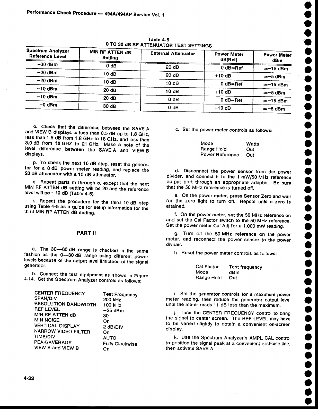
Performance
Check
procedure
_ 4g4Ll4g4Ap
Servlce
Vol.
1o
o
a
o
o
o
O
o
o
a
o
I
o
o
o
I
o
I
o
o
)
I
o
o
I
o
a
o
a
I
I
a
a
o
t
t
a
a
o
a
a
a
o
o
o. Check
that the difference
between
the SAVE
A
and
V|EW
B_disptays
is
tess
than
O.S
dB
up
to 1.g
GHz,
less
than 1.5
dB from
.t.g
GHz
to 1g
GHz,
and
tess
than
3.0
dB from 18
GHZ to 21
GHz. Make
a note of the
level difference between the SAVE
A and VIEW
B
displays.
p. To check
the next 10
dB step,
reset
the
genera_
!o^r lor a 0 dB power meter reading,
and replace
the
20
dB attenuator
with
a 10
dB attenuitor.
_ - _e. I"peat parts m through
o, except
that
the next
MfN
RF AfiEN dB setting
witt
Ue 20
and
rhe
reference
levelwill
be
-10 dB
flabte
4-5).
. r. lepeat,the procedure
for the third 10
dB step
lfing__T19le-4-5
as a guide
for setup
information
for th€
third MIN
RF
ATTEN
dB setting.
PART
II
a. The 30-60 dB range is checked
in the same
fashion
as the 0-30 dB range
using different
power
levels
because
of the
output
level
limitition
of the
signal
generator.
b. Connect
the
test
equiprnent
as shown
in
Figure
4-14.
Set
th€
Spectrum
Analyzer
controls
as
follows:
Tabte
4-5
O TO
30
dB RF
ATTENUATOR
TEST
SETTINGS
Test
Frequency
200
kHz
100
kHz
-25 dBm
30
On
2
dB/Dtv
On
AUTO
Fully
Clockwise
On
c. Set
the
power
meter
controls
as
follows:
Mode Watts
Range
Hold Out
Power
Reference Out
d. Disconnect
the power s€nsor
from th€ power
divider,
and connect
it to the 1 mW/S0
MHz reference
output port through
an appropriate
adapter. Be sure
that
the 50 MHz
reference
is turned off.
e. On
the power
meter,
press
SensorZero
and
wait
for the zero light to turn off. Repeat
until a zero is
attained.
f. On
the
power
meter,
set
the
S0 MHz
reference
on
and set the Cal Factor
switch
to the
S0 MHz reference.
Set
the
power
meter
Cat
Adj
for a 1.000
mW
reading.
g. Turn off the 50
MHz reference
on the power
meter, and reconnect
the power sensor
to the power
divider.
h. Reset
the
power
meter
controls
as follows:
Cal
Factor Test
frequency
Mode dBm
Range
Hold Out
i. Set
the generator
controls
for a maximum
power
meter reading,
then reduce
the generator
output tevel
until
the
meter
reads
't
1
dB less
than
the
maximum.
j. Tune
the CENTER FREQUENCy
conrrot
to bring
the signal
to center
screen. The REF
LEVEL may
have
to be varied
slightly
to obtain
a convenient
on-screen
display.
k. Use
the
Spectrum Analyzer's
AMPL
CAL
control
to position
the signal
peak
at a convenient
graticule
line,
then activate
sAvE A.
CENTER
FREQUENCY
sPAN/DtV
RESOLUTION
BANDWIDTH
REF
LEVEL
MIN RF ATTEN dB
MIN
NOISE
VERTICAL
DISPLAY
NARROW
VIDEO
FILTER
TrME/DtV
PEAK/AVERAGE
VIEW
A
and
VIEW
B
Spectrum
Analyzer
Reference
Level
-30 dBm
MIN RF ATTEN dB
Setting External
Attenuator Power
Meter
dB(Rel) Power
Meter
dBm
0dB 20
dB 0 dB:Ref --15 dBm
:-5 dBm
--lA;
=-5 dBm
-20 ctBm
-20 dBm
-10
dB,"
-10
clBm
10
dB 20 dB +10
dB
10
dB 10
dB 0 dB-Ref
20 dB 10
dB +10
dB
20
dB 0dB 0 dB-Ref :-15 dBm
:-5 dBm
-0 dBm 30
dB 0dB +10
dB
4-22
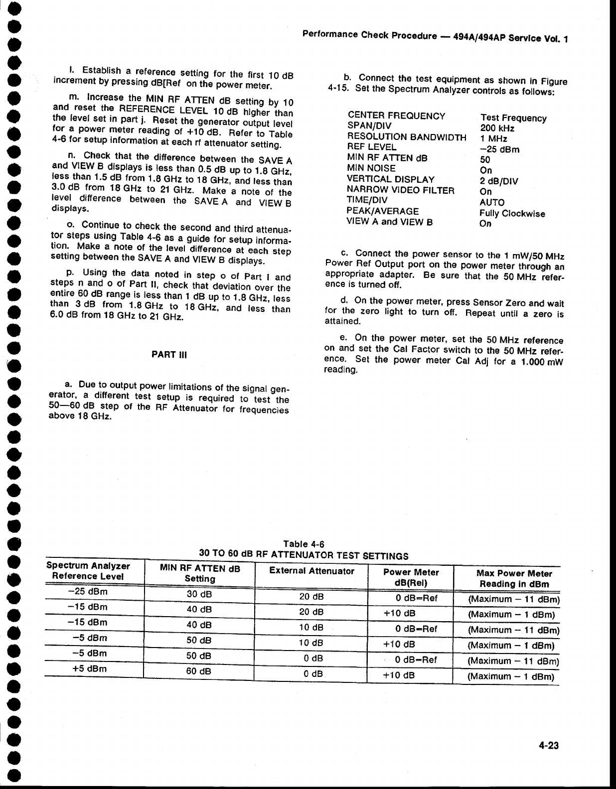
o
I
)
o
o
o
o
o
a
I
o
o
I
o
t
I
t
a
I
o
o
o
o
o
I
O
o
o
o
I
o
o
t
o
a
t
I
I
a
o
o
t
I
o
Performance
Check
procedure
- 4g4Al4g4Ap
Servlce
Vol.
1
b. Connect
the test eguipment
as shown
in Figure
4-15. Set
the
Spectrum
Anatyzer
controls
as
followj:
l. Establish
a reference
setting
for the first 10
dB
increment
by
pressing
dB[Ref on
tie po*"i meter.
m. Increase
the
tr4tN
RF ATTEN
dB setting
by 10
and reset
the REFERENCE
LEVEL
10
dB higher
than
the levet
set in part j. Reset
tn" !"n"i"i* output
level
for a power
meter
reading
of +16
Oe. Eeter to Tabte
4-6
for setup
information
ai each
rf attenuaior
setting.
n. check that the difference
between
the SAVE
A
and
VIEW.B_displays
i9
t^e1
than
0.5
dB
up
to .t.A
GHz,
less
than
1.5
dB
from
1.9
GHz
to f
g Gftz,
lnd tess
than
3.0
dB from 1g
GHz
to 21
GHz. frrt"f."'"
'note
of the
level difference
between
the SAVE
A and VIEW
B
displays.
o. Continue
to cheek
the
second
and
third
attenua-
tor steps
using
Table
4;6 as a guide
for setup
informa-
tion. Make
a note
of the level
liference at each
step
setting
between
the
SAVE
A and
VIEW
B ctisptays.
p. Using
the data noted in step o of part I and
steps n and
o of part lt, check
that deviation
over
the
entire
60
dB
range
is
less
than
I dB
up
to 1.g
GHz,
teis
than
3dB from 1.gGHz
to lgGH;, and tess
than
6.0
dB from
1B
GHz
to
21
GHz.
PART
III
.a. Due
to-
output
power
limitations
of the signal
gen-
erator, a different
test setup is required
to test the
50-60 dB step of the RF Att€nuator
foi frequencies
above
18
GHz.
CENTER
FREQUENCY
SPAN/DlV
RESOLUTION
BANDWIDTH
REF
LEVEL
MIN
RF ATTEN
dB
MIN
NOISE
PEAK/AVERAGE
VIEW
A and
V|EW
B
Test
Frequency
200
kHz
1
MHz
-25 dBm
50
On
Fully
Clockwise
On
VERTICAL
DISPLAY 21BIDIV
NARROW
VTDEO
FILTER On
TIME/DIV AUTO
^ c. !o1n_ect
the power
sensor
to the
1 mW/50
MHz
Power
Ref
Output
port_on
the power
meter
through
an
appropriate
adapter. Be sure that the 50 MHz iefer-
ence
is
turned
off.
d. On
the
power
meter, press
SensorZero
and
wait
for the zero light to turn off. Repeat
untit
a zero is
attained.
e. On the power
rneter,
set the 50
MHz reference
on and set the Cal Factor
switch
to the
S0 MHz refer-
ence. Set the power
meter
Cal
Adj for a 1.000mW
reading.
Table
4-6
30
TO
60
dB
RF
ATTENUATOR
TEST
SETTINGS
Spectrum
Analyzer
Reference
Level
-25 dBm
-15
dBm
--15
dBm
-5 dBm
MIN
RF
ATTEN
dB
Setting External
Attenuator Power
Meter
dB(Rel) Max Power Meter
Reading
In dBm
30
dB 20 dB 0 dB-Ref (Maximum
- 11
dBm)
40 dB 20
dB +10
dB (Maximum
- 1 dBm)
40
dB 10
dB 0 dB-Ref (Maximum
- 11
dBm)
50
d8 10
dB +10
dB (Maximum
- 1
dBm)
-5 dBm 50
dB 0dB 0 dB:Ref (Maximum
- 11
dBm
+5
dBm 60 dB 0dB +10 dB (Maximum
- 1
dBm)
4-23
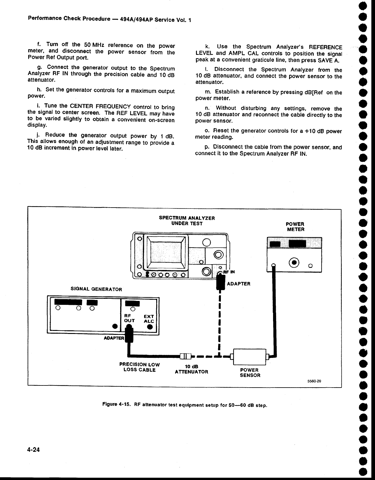
Performance
Check
procedure
- 4g4Al4g4Ap
Service
Vot.
1
f. Turn off the 50 MHz reference
on the power
rneter, and disconnect
th€ power sensor from the
Power
Ref
Output
port.
- g. Collect the generator output to the Spectrum
Analyzer
RF lN through
the precision
cabte
and 10
dB
attenuator.
h. Set the
generator
controls
for a maximum
output
power.
i. Tune
the CENTER
FREQUENCy
controt
to bring
the signal to center
screen. The
REF
LEVEL
may
hav6
to be varied
slightly
to obtain
a convenient
on-screen
display.
_- j. Reduce the generator
output power by 1 dB.
This allows
enough
of an
adjustment
range
to piovide
a
10
dB increment
in power
level later.
k. Use the Spectrum Anatyzer's REFERENCE
LEVEL and AMPL CAL controls
to position
tho signal
peak
at a convenient
graticule
line,
then
press
SAVE A.
l. Disconnect
the Spectrum Analyzer from the
10
dB attenuator,
and
connect
the power
sensor
to the
attenuator.
m. Establish
a reference
by pressing
dB[Ref on
the
power
rnet€r.
n. Without disturbing any settings, remove th€
10
dB attenuator
and
reconnect
the cable
directly
to the
power
sensor.
o. Reset
the
generator
controls
for a +10 dB power
meter
reading.
p. Disconnect
the cable from
the
power
sensor,
and
connect it to the Spectrum
Analyzer
RF lN.
o
o
t
o
a
o
o
o
o
a
o
I
o
o
I
I
a
a
a
o
o
o
o
o
I
o
o
o
t
o
I
o
o
o
I
t
t
a
a
o
o
a
I
I
SPECTRUM
ANALYZER
UNDER TEST POWER
METER
SIGNAL GENERATOR
I
I
I
I
I
I
I
--J
PRECISION
LOW
LOSS
CABLE 10
dB
ATTENUATOR POWER
SENSOR
4-24
Figure
4-15. RF attenuato. test equipment setup for 50-60 dB step.
o
I
a
o
o
o
o
o
o
a
o
I
o
o
I
I
,
o
I
o
I
a
o
o
a
a
a
o
a
o
O
a
I
o
o
t
I
t
o
o
O
a
I
o
.. q: 19.gt the
Spectrum
Analyzer
RF
attenuator
set-
ting to 60
dB, and increase
the reference
level
setting
by
t0 dB.
.r, lheck that t,€ {itEreqce between
the SAVE
A
and.
VIEW
g.gi.prqfr is \ss t\"n s.ri
o-e. Make
a note
of th€
levet
differe(rce
OetNqer/ttre
SnVe
n'anO
V|EW
B
displays. \
s. Using
the
data
noted
in step
o of part l, steps
n
and
o of part
ll, and
step
r of part
ttt,
ctreck
that
devia-
tlon
over
the
entire
60
dB range
is
less
it "n'O
Og.
18.
Check
lF Gain
Accuracy
(+0.2.dB/dB
Step
to a miximum
of *0.S dB/g
dB
except
at the
decade
transitions
of _19 Oem
to _eO
dBm,
-29 dBm
to __30
dBm,
_3s
oam
to
_40
dBm,
-49 dBm
ro -S0 dBm, and _59 dBm io _60 oBm
where
an
additional
O.S
dB can
occur
foi a totat
of t
dB/decade.
Maximum
deviation
over
the full
g7 dB
range
is
within
+2 dB)
.. T.hf".check
requires
calibrated
attenuators
to check
the 10dB and 1 dB steps. When
mafing
measure-
ments
within
10
dB of the noise
floor,
a correction
fac-
tor should
be used
to correct
for the logarithmic
addi-
tion
of noise
in
the system,
as
shown
in
fi6te +-2.
a. Connect
th€ test equipment
as shown
in Figure
4-13,
using
the calibrated'1d
dB ano
t ae attenuators
!"j ::g^::l the output
-of the g"n"r"to, oirecily to the
RF TNPUT
if individuat
fixed
atGnu"tor"
"r"1o be used
as lhe standard).
Set th€ Spectrum
Analyzer
controls
as
follows:
Performance
Check procedura
- 4g4Al4g4Ap
Servlce
Vol.
1
d. Set the output of the signal generator
to re-
position
the
signal
level
at
the
6th
graticule
line.
e. switch ihe REF
LEVEL
from _10dBm to _20
dBm in I dB steps,
adding
.l dB of externat
att€nuation
at
each
step. Note
incremental
accuracy
and
the 10
dB
91n.jr9g!racy. Incrementat
accuracy
must be within
0.2
dB/dB. Maximum
cumulative
erroi rnust
not
exceed
0.5
dB except when stepping
frorn
the g dB to 10
dB
increment,
where the error could be an addational
0.5
dB. This exception_does
not apply
when
stepping
from
-69 dBm
to _70
dBm,
_79 dBm
to _go oem,
itc.-
f. Deactivate
MtN NolsE. Return
the 1
dB step
attenuator
to 0 dB, decrease
the output of the sign;l
generator
by 10
dB or add l0 dB of external
attenua-
tion. Reset
the generator
output
so the signal
tevet
is
again
at the
6th
graticule
line.
-9. change the REF LEVEL from _20
dBm to
-30 dBm, in 1
dB increments,
with the 1
dB stef
attenuator,
and note
incremental
and 10
dB step
accu-
racies.
h. Return the 1
dB step attenuator to 0 clB.
Decrease
the signal level by 10
dB with external
attenuation,
or with the signat generator
output fevel
control, then re-estabtish
the signal reference
ampli_
tude.
i. Check
the -30 dBm
to -40 dBm gain
accuracies
as in
part
e.
j. Repeat
the procedure
checking
gain accuracies
to
-60 dBm.
CENTEB
FREOUENCY
SPANIDtV
RESOLUTION
BANDWIDTH
REF
LEVEL
MIN
RF
ATTEN
dB
VERTICAL
DISPLAY
WIDE
VIDEO
FILTER
TrME/DtV
SAVE
A
100
MHz
10
kHz
10
kHz
-10
dBm
0
1
dB/Dlv
On
AUTO
off
k. Establish a signal reference
-60 dBm, activate NARROW VTOEO
check gain
accuracy
to -70 dBm.
amplitude of
FILTER, then
- b. Set
the generator
controls
for a 100
MHz
output
frequency,
and
a signal
amplitude
ot six
Oivisions.
c. Activate
MIN
NOISE
and
note
signal
level
shift.
Level
shift
must
not exceed
*0.g dB, o-,
+ minor
Oiui_
sions
(attenuator
plus
gain
accuracies).
I. Decrease
the RESOLUTION
BANDWIDTH
and
SPAN/DIV
to 1 kHz. Re-establish
a signal reference
level
of -70 dBm
as
described
previously.
m. Check
the -70 dBm to -90 dBm gain accura-
cies
by
repeating
the
process
previously
deicribed.
n. Decrease the RESOLUTTON
BANDWTDTH
100 Hz and SpAN/DIV
to 50 Hz, reestabtish
the signal
reference
level
and check
the -g0 dBm to _gO
dBm
and -90dBm to -1
00dBm gain accuracies.
These
ranges
are
directly
related
to the
-60 dBm
to _70
dBm
check (parts
d through
m).
CORRECTION
FACTOR
TO DETERMINE
TRUE
STGNAL
LEVEL
Table
4-7
dB Ratio
of Signal
Plus
Noise 3.0 4.0 5.0 6.0 7.0 8.0 9.0 10.0 't2.0 14.0
Correction
Factor 3.0 2.20 1.65 1.26 0.97 0.75 0.s8 0.46 4.28 0.18
4-25

Performance
Check
procedure
- 4g4Al4g4Ap
Service
Vol.
1
19. Check Gain Variation Between Resolution
Bandwidths
(Less
than *0.4 dB with respect
to the
3 MHz fitter
and
less
than
0.8
dB between any
two filters)
Before
performing
this check,
do a front panel
CAL
procedure
by pressing <Blue-SHIFT> CAL and per_
forming
the steps
prompted
by the spectrum
analyzer.
a. Apply
the
CAL
OUT
signat
to the RF
tNpUT, and
set
th€
Spectrum
Analyzer
controls
as
follows:
CENTER
FREQUENCY 100MHz
SPAN/DIV 100
kHz
RESOLUTION
BANDWTDTH 3 MHz
REF LEVEL -18 dBm
b. Enable a marker by pressing
TUNE
CFIMKR.
Tune the
marker
to the highest
point
on the
noise
floor.
Activate zERo SPAN, and change
the RESoLUTIoN
BANDWIDTH
to 3 MHz and
the REFERENCE
LEVEL as
ncessary
to view
the
baseline.
c. Check
that the noise
floor
(level)
is down as per
Table 4-8 (at least
-80 dBm down if checking
a stan-
dard instrument,
or -31 dBmV if checking
the 7SO
input in an
Option
07 instrument).
The REF LEVEL will have to be reset each
tiME thE RESOLUTION BANDWIDTH iS
changed.
d. RESET
thE RESOLUTION
BANDWIDTH
tO 1 MHZ.
e, Check that the noise floor (level)
is down as per
TablE
4-8.
f. Reset the RESOLUTION BANDWTDTH to
1 00 kHz.
g. Check that the noise floor (level)
is down as per
Table 4-8.
h. RESET
thE
RESOLUTION BANDWIDTH
tO
1O KHZ.
i. Check that the noise floor (level)
is down as per
Table 4-8.
j. Reset
the RESoLUTION BANDWTDTH
to 1 kHz.
k. Check that the noise floor (level)
is down as per
Table 4-8.
I. RESET
thE
RESOLUTION
BANDWIDTH
tO
1OO HZ.
m. Gheck that the noise floor (level)
is down as per
Table 4-8.
N. RESET
thE RESOLUTION
BANOWIDTH
tO 1O HZ.
and VERTICAL
DISPLAY
to 5 dB/DlV.
o. Check that the noise floor {level)
is down as per
Table 4-8.
p. Repeat this procedure for the remaining
coaxial
input frequency
range (1
.7 to 21 GHz). lf desired,
the
sensitivity
for the waveguide bands can be checked as
per the listings in Table 4-8. The values for the 50 GHz
to 140 GHz range are typical and not intended as a per-
formance requirement.
FREQ
RANGE
sPAN/DrV
RESOLUTION
BANDWIDTH
REF LEVEL
MIN
RF ATTEN
dB
VERTICAL
DISPLAY
NARROW
VIDEO
FILTER
VIEWA&VIEWB
PEAK/AVERAGE
TrME/DrV
0-1.8 GHz
MAX
10
kHz
-100
dBm
0
2 dBlDlV
On
On
Fully
Clockwise
1s
o
o
o
a
a
o
o
o
o
a
o
I
o
I
I
t
I
I
a
o
a
O
o
o
a
o
o
o
o
o
I
o
o
o
O
I
a
a
a
o
a
o
o
o
MlN
RF
ATTEN
dB
VERTICAL
DISPLAY
MIN
NOISE
TrME/D|V
0
1
dB/Dtv
On
AUTO
b. Activate
the AA
mode
by
pressing
FINE.
c. Reset
the
REFERENCE
LEVEL
controt
to position
the calibrator
signal
at the 7th graticule
line (1 major
division from the top), then
activate
SAVE
A to store
the
3 MHz
amplitude.
d. Change the RESOLUTTON
BANDWTDTH
to
1 MHz.
e. check that amplitude
deviation
from the 3 MHz
referenc€
is no
more
than *0.4 dB.
f. Change the RESOLUTTON
BANDWTDTH
to
100
kHz
and
the FREQ
SpAN/Dtv
to .t0
kHz.
g. Check
that amplitude
deviation
from the 3 MHz
reference
level
is no more
than
f 0.4
dB.
h. R€p9at
the procedure
to check the remaining
filters
(10kHz,
1
kHz, 100H2,
and 10
Hz)
to verify
that
the signal amplitude does not change more than
+0.4 dB from
the
3 MHz reference
level.
i. Check variation
between any two filters (0.g dB)
by finding
the filter
that has
the lowest
amplitude,
sav_
ing
it on the A-trace,
then
comparing
the other
filters
to
the saved
trace.
20. Gheck Sensitivity
(Refer
to Table
4-8)
a. conn€ct
the cAL ouT signat
to the RF tNpuT,
and perform
th€ <Blue-SHIFT>
CAL routine.
Remove
the
CAL
OUT signal
from
the RF lNpUT,
and
terminate
the FF INPUT
in its characteristic
impedance.
Set
the
Spectrum Analyzer
controls
as
follows:
4-26
o
o
I
o
o
o
o
o
o
a
o
o
o
o
o
o
I
o
I
I
O
a
O
o
o
o
o
o
o
o
a
a
I
o
o
a
I
o
I
a
o
o
o
a
Performance
Check
procedurc
- 4g4Ll4g4Ap
Service
Vol.
l
Table
4-8
SENSITIVITY.
tN
dBm
(dBmV
for 75o tNpUT)
21. Gheck Residual
Spurious Response
With
no
input
signat,
-100 dBm
oi tessl
_a.
Remove
any
signal
connected
to the
RF
lNpUT,
and
terminate
the RF
tNpUT
in 50O. Set
the
Spectrum
Analyzer
controls
as
follows:
CENTER
FREQUENCY 50
MHz
SPAN/DIV 10
MHz
RESOLUTION
BANDWIDTH 10
kHz
REF
LEVEL -50 dBm
b. Press <Green-SHIFT>
STEP
SIZE to estabtish
a center
frequency
step size. This
will allow
changing
center
frequency
in 50 MHz increments
by use of the
+STEP
and
-STEP pushbuttons.
c. Scan the frequency range
of bands
"1
, Z, o( S in
100
MHz increments.
Note
the amplitude
of any
spuri-
ous response.
Spurious response
amplitudes
must not
exceecl
-1 00 dBm. (Activating
A F after each incre-
ment,
makes it easier
to determine
100
MHz incre-
ments.)
MIN RF ATTEN dB
VERTICAL
DISPLAY
TrME/DtV
0
10
dB/Dtv
AUTO
a Equivalent
maximum inPut noise (average nois€ {or €sch resolution bandwidth with int€rnal mixer and rEKTRoNtx waveguide Mixers),
b Option 07 reptaces the 100 kHz filter with a 300 kHz filter.
c TEKTRONIX
Waveguide
Mixers.
Band/Frequency I MHz 1 MHz 300 kHzb 100
kHz 10
kHz 1 kHz 100
Hz 10
Hz
eanQ | (cut,
Input)
10 kHz-l.8 GHz -80 -85 -90 -95 -105 -115 -12s -134
\rPuon
u/ (/5{r Input)
5 MHz-l GHz -31 -36 -41 NA -56 -66 -76 -85
E anss z 6(
U (5U{1,
Input)
1.7
GHz-7.1 GHz -74 -79 -u -89 -99 -109 -119 -125
E
ano
4 (curl tnput)
5.4-12 GHz -60 -65 -70 -75 -85 -95 -105 -111
Band
4 (50o Input)
12-18 GHz -55 -60 -65 -70 -80 -90 -l 00 -107
uano
] (5utr
tnput)
15-21 GHz -55 -60 -oc -70 -80 -90 -100 -'t07
bano bs (5o{} Input)
78-27 GHz
-65 -70 -75 -80 -90 -100 -108 -116
E anos
/ ar
ue
(5uo
Input)
26-60 GHz
Band
9c
(50O
Input)
50-90 GHz
Band
10c
(50o Input)
7$-140 GHz
-
Band
11c
(50O
Input)
110-220
GHz
Bandl2c (50O
fnput)
170-325
GHz
-60 | -65 -74 -75 -85 -9s | -103 | -trr
ypically
-95 dBm for 1 kHz
resolution
bandwidth
at 50
GHz, degrading
to -g5 oam at g0
iHz
ypically
-90 dBm
for 1 kHz resolution
bandwidth
at zs aHz, oegrading
to -7s oam ai
40
GHz
ypically
-80 dBm for 1 kHz resolution
bandwidth
at 110
enr, o"graoing
to -65 dBm
at
20
GHz
ypically
-70 dBm for 1 kHz resolution
bandwidth
at 170
GHz, degrading
to -55 dBm at
25
GHz
4-27
Performance
Check
procedure
- 4g4A/4g4Ap
Service
Vol.
1
Spactum Analtrar Un(br Totl
al|C T{oilt clot
Figure 4'16. Test equlpment setup for checking intermoduration
distortion.
o
o
t
o
a
o
O
a
o
I
o
I
o
a
o
I
I
a
o
t
o
o
o
o
o
o
o
o
o
o
t
o
o
o
t
I
C
a
a
O
o
o
o
o
freq.-..t, f1 t2
Third (3rd)
Order Intermodulation
products 2127_.ts
Figure
4-17. Intermodulatlon
products.
b. Set the generator
outputs approximately
2 MHz
apart
within the
frequency
range of band
1, and
set the
output
levels for full
screen
signals.
c. Decrease
the separation
of the generator
fre-
quencies
to 1 MHz. Reset
the spAN/Dlv
to 500 kHz
And
RESOLUTION BANDWIDTH
to 1O KHz.
d. Check
that the third order lM products
are at
least
70 dB down trom the input signal level. See Fig-
ure 4-17.
Use
the Video
Filter
and very
slow sweep
rates
to help resolve
these
sidebands.
e. Decr€ase
the signal separation and SPAN/DIV
settings and
re-check
for sidebands.
Check
for
lM pro-
ducts at olher spans
of the frequency
range. lM pro-
ducts
should
be
-70 dBc or more.
f. Change the FREQUENCY
RANGE
to Band 2
(1.7-5.5 GHz),
FREQ
SPAN/DIV
to 5
MHz,
and RESO-
LUTION
BANDWIDTH
to 100
kHz.
g. Reset the generator outputs approximately
2 MHz
apart within
the frequency
range
of band 2, and
set
the output levels
for full
screen
signals. Reduce
the
SPAN/DIV
and
RESOLUTION
BANDWIDTH so
the noise
floor is
at least
70
dB down from
the
reference
level.
h. Check that lM products
are
at least 70
dB down
from
the
input signal
level or
top
of
the
screen.
22.
Check Intermodutation
Distortion
fl-hird
order
products
at least
70
dB down from
anv
two
on-screen
signals)
a. connect
the
test equipment
as shown
in Figure
4-16, and set the Spectrum
Analyzer
controls
as fol-
lows:
FREO RANGE
CENTER FREQUENCY
sPAN/DrV
RESOLUTION
BANDWIDTH
REF LEVEL
MIN
RF ATTEN
dB
VERTICAL
DISPLAY
TrME/DrV
4-28
0-1.8 (Band
1)
Within 2 MHz of
Test Generators
5 MHz
100
kHz
-30 dBm
n
10
dBiDrv
AUTO
o
o
o
o
I
o
s
o
)
o
o
o
o
o
I
I
I
t
I
I
I
a
o
o
o
o
o
o
o
t
a
I
a
o
o
a
I
I
o
a
t
a
I
a
23. Check Harmonic
Distortion
{-60 dBc
or
tess
frorn
10
kHz
to 1.g
GHz)
{Not discernible
above
tt " "u"r"g" no]r" ftoor
(at
teast
100
dBc)
from
1.7
GHz
to
21-cHti
Tested
at -90 dBm
in
MIN
DTSTORTTON
mode
a. Gonnect
the test equipment
as shown
in Figure
4-18, and set the Spectrum-
Analyzer
"onirolu
as fol_
lows:
Performance
Check
procedure
- 4g4Al4g4Ap
Service
Vd. l
CenterFrequency 2O72MHz
Span/Div 2MHz
Min
RF Atten
dB 0
Verticat
Display t0dB/DtV
Time/Div Auto
Triggering Free
Run
Baseline
Clip Otr
Reference
Level -70 dBm
Auto
Resolution On
View
A and
View
B On
Mdeo
Filter Wide
Peak/Average Fully
Clockwise .
b. Set
the Spectrum
Analyzer
under
test
as foltows:
CENTER
FREQUENCY 0Hz
REF
LEVEL -30 dBm
SPAN/DIV 100
kHz
.b. Note
the Spectrum
Analyzer
display
as the
gen-
erator
frequency
contror
is variid auoui
ilie center
fre-
quencyof
the
bandpass
filter
if a bandpass
filter
is used
in the test, or as the frequency
is varied
below
the
cutoff
frequency
if a low pass
filter
is
used.
Set the generator
frequency
at that frequency
that
yielded
the maximum
amplitude
in part
b, then
set
the output
tevet
for a fuil
screen
(_30
Oelny
iign"t.
In
Figure
4-18,
the
filter
shown
must
have
a
minimum
of 40
dB rolloff
to attenuate
multi_
ples of the generator
frequency,
and the
frequency
ot the signal
generator
depends
on
the frequency
characteristics
of the
fitter.
d. SEt thE CENTER FREQUENCY tO
!2jlLq$lequency), FREQ
SPAN/D|V
to 500
kHz,
and
RESOLUTTON
BANDWTDTH
to 10
kHz.
e. Check
that the
second
harmonic
of the input
sig_
nal
is at least
60
dB
below
the
-90 dBm carrier.
f. SEt
thE CENTER
FREQUENCY
tO thE 3rd hAr.
monic.
g, Check
that
the
third
harmonic
of the
input
signal
is at least
60 dB down from
the
-30 dBm carrier.
CENTER
FREOUENCY
sPAN/DtV
AUTO
RESOLN
REF
LEVEL
MIN
RF
ATTEN
dB
VERTICAL
OTSPLAY
WIDE
VIDEO
FILTER
MIN
DISTORTION
VIEW
A and
V|EW
B
TrME/DtV
Same
as Genera-
tor
5 MHz
On
-30 dBm
0
10
dB/Dlv
On
On
On
AUTO MIN
RF ATTEN
dB
PEAK/AVERAGE 0
Fully
Clockwise
1.7
GHz
100 kHz
On
-30 dBm
0
10
dB/Dtv
On
AUTO
c. Check for any
indication
of LO emission.
LO
ernission
must
be fess
than
-70 dBm.
25.
Check
1
dB
Compression
point
(-20
dBm Bands
I through
5)
Calibrate
the power meter befora making
this
measurement.
a. Use
the power
meter
to set
the
output
level
of a
signal
generator
to 0 dBm at
1.7
GHz.
b. Connect
the test equipment
as shown in Figure
4-19, using th€ generator
with the calibrated
output
level. Set
the
Spectrum Analyzer
controls
as followsi
CENTER
FREOUENCY
sPAN/D1V
AUTO
RESOLN
REF
LEVEL
MIN
RF ATTEN
dB
VERTICAL
DISPLAY
VIEW
A and
VIEW
B
TIME/DrV
24.
Check
LO
Emission
(-70
dBm
or
tess)
a. Monitor the RF INPUT with a hioh
spectrum analyzer such as a 4g2A. Set tie
trum analyzer
controls as follows.
frequency
test
spec-
4-29
c. Set the attenuators
for
25 dB of attenuation.
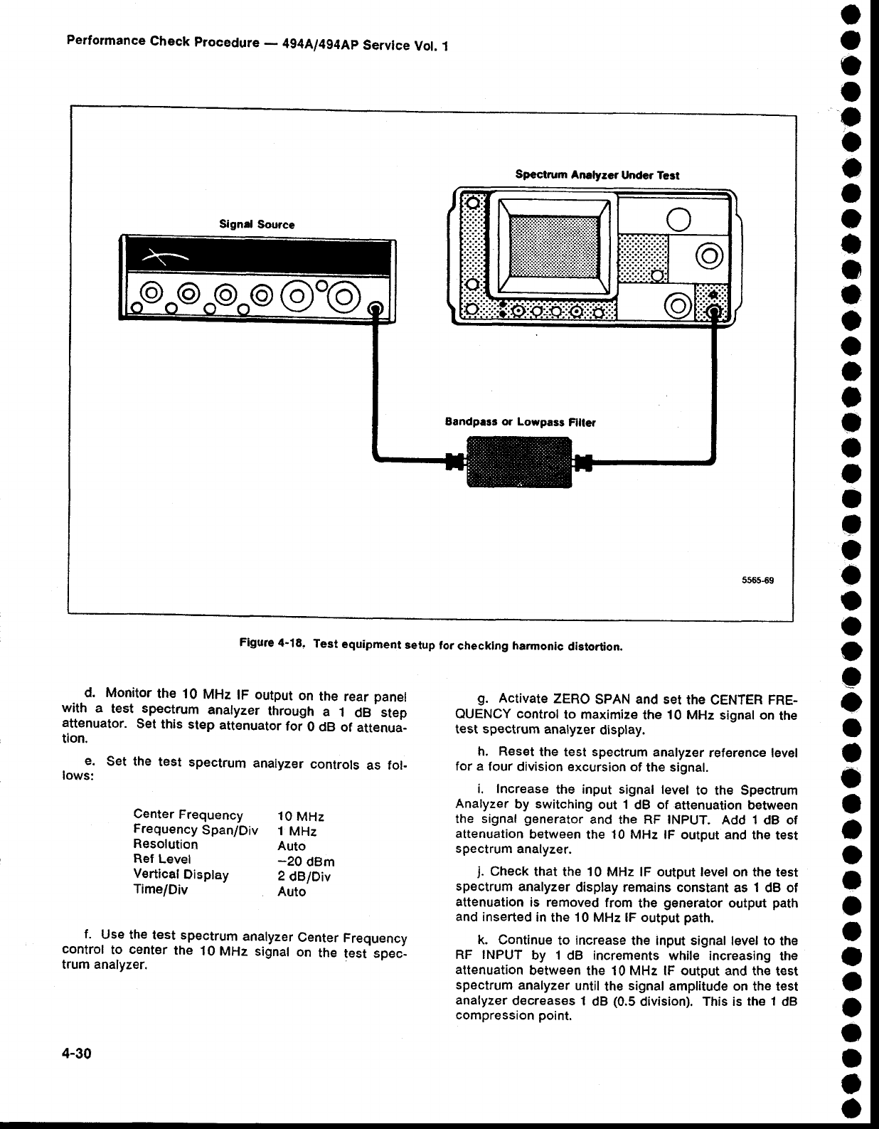
Performance
Check
procedure
- 4g4Al4g4Ap
Service
Vol. 1
Spectrum
Analyeer
Under Test
Figure
4-18. Test
equipment
setup
lor checklng
harmonic
distortion.
d. Monitor
the
10
MHz
lF output
on
the
rear
panel
with a test sp€ctrum
analyzer
through
a 1 dB step
attenuator.
Set
this step
attenuator
for 0 clB
of attenua-
tion.
e. Set the test spectrum
analyzer
controls
as tol-
lows:
Center
Frequency 10
MHz
Frequency
Span/Div i MHz
Resolution Auto
Ref
Levet _20 dBm
Vertical
Disptay 2
dB/Div
Time/Div Auto
f. Use the
test spectrum
analyzer
Center
Frequency
control
to cent€r
the 10
MHz signal
on the
test spec-
trum analyzer.
g. Activate
zERo spAN and set
the CENTER FRE-
OUENCY control
to maximize
the
10 MHz
signal on
the
test spectrum
analyzer
display.
h. Reset
the test spectrum
analyzer
referEnce level
for
a four
division excursion
of
the
signal.
i. Increase
the input signal
level
to the Spectrum
Analyzer
by switching
out 1 dB of attenuation
between
the signal
generator
and the RF INPUT.
Add
1
dB of
attenuation
between
the
10
MHz lF output and
the
test
spectrum
analyzer.
j. Check
that the 10
MHz lF output level on the test
spectrum
analyzer
display
remains
constant
as 1
dB of
attenuation
is removed
from
the generator
output
path
and
inserted
in
the 10 MHz lF output
path.
k. Continue
to increase
the input signal
level to the
RF INPUT
by 1
dB increments while increasing the
attenuation
between
the 10 MHz lF output and the
test
spectrum
analyzer
until
the
signal
amplitude on
the
test
analyzer
decreases
1
dB
(0.5
division). This is
the 1
dB
compression
point.
4-30
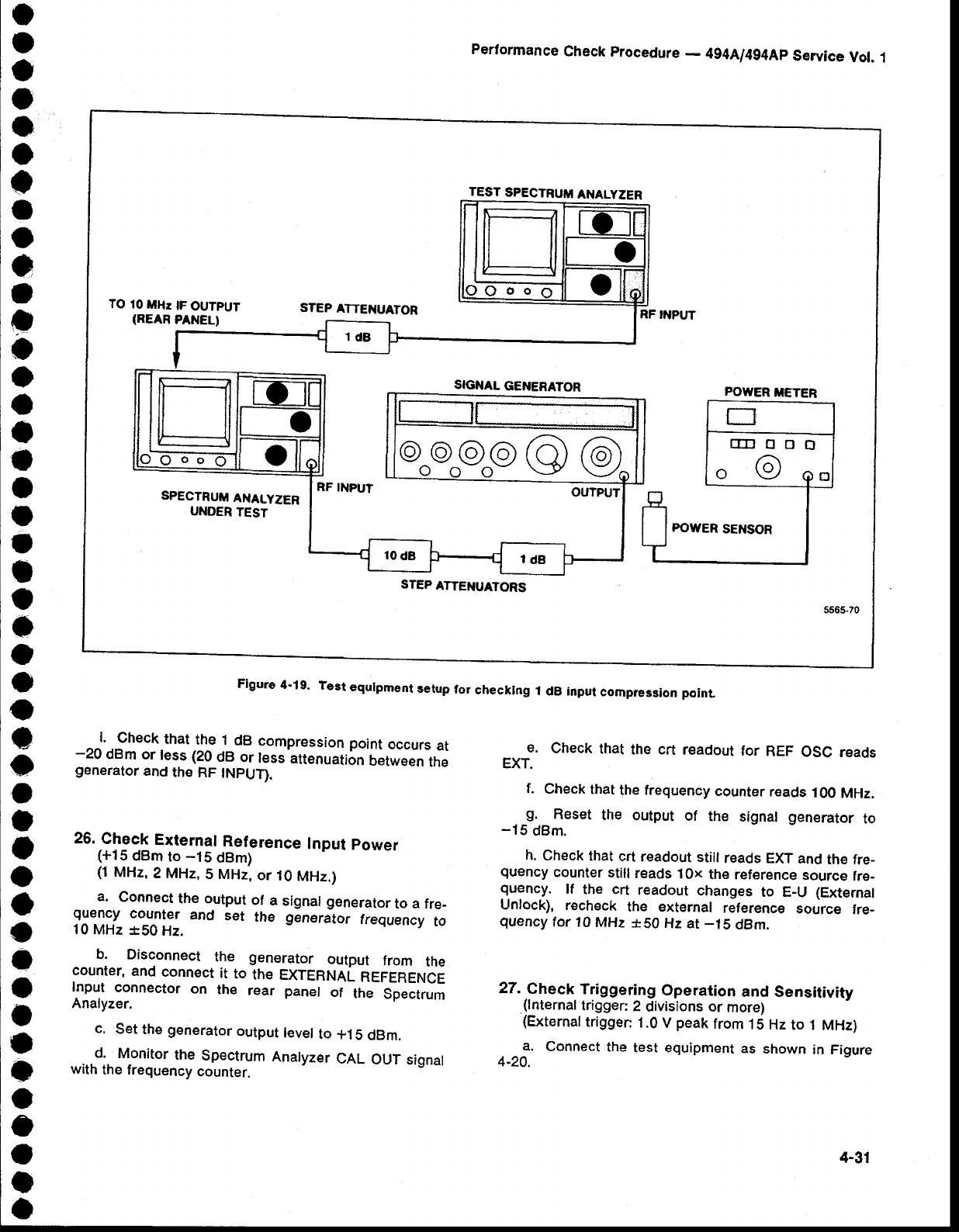
o
I
o
o
o
o
o
I
o
e
I
o
o
o
a
o
{l
I
I
a
I
o
o
a
o
o
e
o
o
I
o
o
o
o
i
o
I
I
o
a
C
o
o
a
l. Check
that
the 1 dB compression
point
occurs
at
-20 dBm
or less (20
dB
or less
attenuation
Oetween
the
generator
and
the
RF
INPUT).
26.
Check External
Reference
Input power
(+15
dBm
to
-15 dBm)
(1
MHz,
2 MHz,
5
MHz,
or
10
MHz.)
a. Connect
the output
of a signal generator
to a fre-
quency
counter and set the generator
frequency
to
10
MHz
*50 Hz.
b. Disconnect the generator output from the
counter,
and
connect
it to the EXTERNAL
REFERENCE
Input connector
on the rear panel of the Spectrum
Analyzer.
c. Set
the
generator
output
level
to *1
5
dBm.
...d..
Monitor
the
Spectrum
Analyzer
CAL
OUT
signal
with
the frequency
counter.
Performance
Check
procedure
- 4g4Al4g4Ap
Service
Vol.
1
e. Check
that the crt readout
for REF
OSC
reads
EXT.
f. Check that
the
frequency
counter
reads
100
MHz.
g. Reset the output of the signal generator
to
-15
dBm.
h. Check
that
crt readout
still
reads EXT
and
the
fre_
quency
counter
still
reads
10x the
reference
source
fre_
quency. lf the crt readout
changes
to E_U (External
Unlock),
recheck
the external reference
source fre-
quency
tor
10
MHz
*S0 Hz at
-15 dBm.
27.
Check
Triggering
Operation
and Sensitivity
.(lnternal
trigger:
2
divisions or
more)
{External
trigger:
1.0
V
peak
from
.t
5 Hz
to 1 MHz)
a. Connect
the
test equlpment
as shown
in Figure
4-20.
TEST
SPECTRUM
ANALYZER
TO
10
tlHz
tF
OUTPUT
(REAR
PANEL) STEP ATTEI{UATOR RF INPUT
SIGNAL GENERATOR
SPECTRUTTI
ANALYZER
UNOER
TEST
RF INPUT OUTPUT
POWER
METER
@o@o@g@@
STEP
ATTENUATORS
Flgure
4'19. Test
equrpment
setup
tor checkrng
1
dB input
compression
poinl
4-31
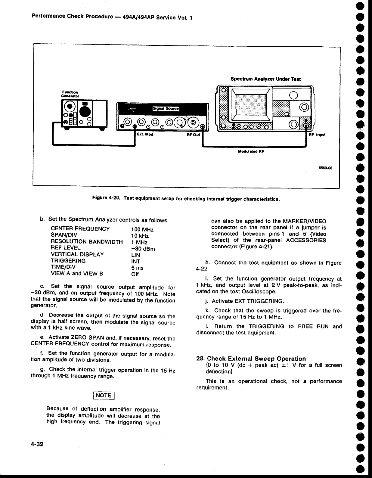
Performance
Check
procedure
- 4g4A/4g4Ap
Service
Vol. l
Speclnm Andyrcr Undcr Tcst
Iodrl.l.d RF
Figure
4'20. Test
equlpment
selup for
checking Intemal
trlgger characteri3tica.
o
a
o
o
a
o
I
a
o
t
t
e
o
a
o
o
o
a
f
o
t
o
a
o
o
O
o
o
o
a
a
o
o
a
a
o
o
a
o
a
c
o
o
a
4-32
b. Set
the Spectrum
Analyzer
controls
as
follows:
CENTER
FREQUENCY 100
MHz
SPAN/DIV 10
kHz
RESOLUTTON
BANDWTDTH 1
MHz
REF LEVEL -30 dBm
VERTICAL
DISPLAY LIN
TRIGGERING INT
TIME/OIV S ms
VIEW
A and
V|EW
B Off
_ c. Set the signal source output amplitude
for
-30 dBm, and an output frequency
of 100
MHz. Note
that
the signal source
will be modulated
by
the function
9enerator.
d. Decrease
the output
of the signal
source
so
the
display
is half screent
then rnodulate
the signal
source
with
a 1 kHz
sine
wave.
e. Activate
ZERO
SPAN and,
if necessary,
reset
the
CENTER FREQUENCY
control
for
maximum
response.
f. Set
the function
generator
output
for a modula_
tion amplitude
of two divisions.
g. Check th€
internal
trigger
operation
in
the 15 Hz
through
1
MHz
frequency
range.
Because
of deflection
amplifier
response,
the display amplitude
will
decrease
at the
high frequency
end. The triggering
signal
can also
be applied
to the MARKER/VIDEO
connector
on the rear panel
if a jumper
is
connected between pins
1 and 5 (Video
Select) of the r€ar-panel ACCESSORIES
connector (Figure
4-21).
h. Connect the test equipment
as shown in Figure
4-22.
i. Set the function
generator
output frequency
at
1 kHz, and output level at 2 V peak-to-peak,
as indi-
cated on
th€ test Oscilloscope.
j. Activate EXT TRIGGER|NG.
k. Check that the sweep is triggered
over
the
fre-
quency
range ot 15 Hz
to 1 MHz.
I. REIUTN
thE TRIGGERING
tO FREE
RUN ANd
disconnect
the
test equipment.
28.
Check External Sweep Operation
{O
to t0 V (dc + peak ac) *1 V for a lull screen
deftection)
This is an operational check, not a performance
requirement.
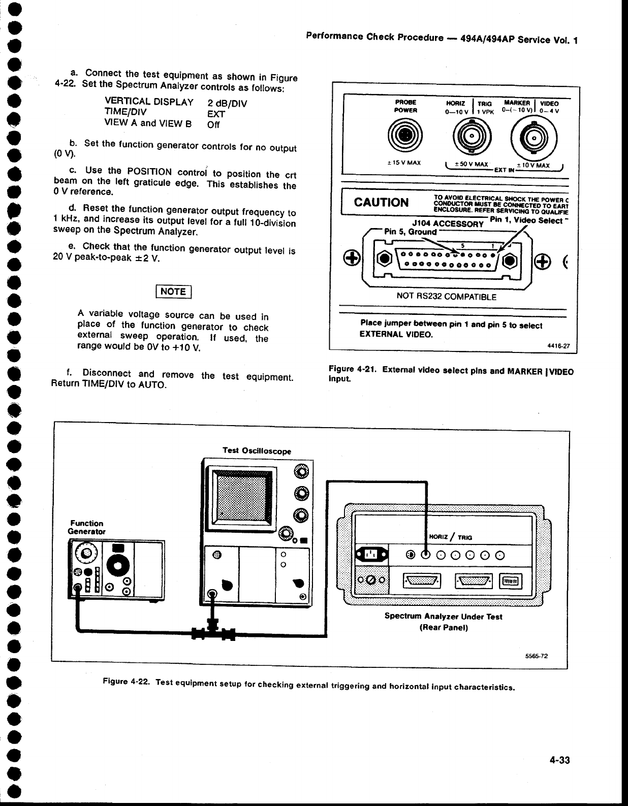
a. Connect
the test eguiprn€nt
as shown
in Figure
4-22. Set
the
Spectrum
enityzer
"ontroi, "i fouows:
VERT|CAL
DTSPLAY 2 dB/DtV
T|ME/D|V EXT
VIEW
A and
V|EW
B Otr
b. Set
the
function
generator
controls
for no
output
(0
v).
c. Use thE POSITION
"ontroi to position
the crt
beam
-on
the left graticule
edge. This'est;btishes
the
0 V
reference.
d. Reset
the
function
generator
output
frequency
to
1
kHz,
and
increase
its output
level
for " trti t O-Oiri"ion
sweep
on
the
Spectrum
Analyzer.
e. Check
that
the function
generator
output
level
is
20
V peak-to-peak
*2 V.
A variable
voltage
source
can be used in
plac€ of the function
generator
to check
external sweep operation, lf used. the
range
would
be
0V
to +10
V.
f, Disconnect
and remove the test equipment.
Return
TIME/DIV
to AUTO.
Perfonnance
Check
procedure
- 4g4ful4g4Ap
Service
Vol. l
Pioa€
POWEF
\s7/^t
t15VMAX
CAUTION
Place jumper between pin I antl pin 5 lo selecl
EXTERNAL
VIDEO.
JIdACC-ESSORIT pin t, Video Setecr -
NOT
RS232
COMPATIBLE
ooooooo?toooo
oooo ococoooo
Figure
4-21. Extemal
vldeo
select
plns
and
MARKER
IVIDEO
Input
Test Oscltloscope
@
@
@
@". ooooooo
Funclion
Generato.
Spectrum Analyzer Under Test
(Rear
Panel)
Figure 4'22' Test equipment setup for checking external triggering and horizontal input characteristics.
4-33
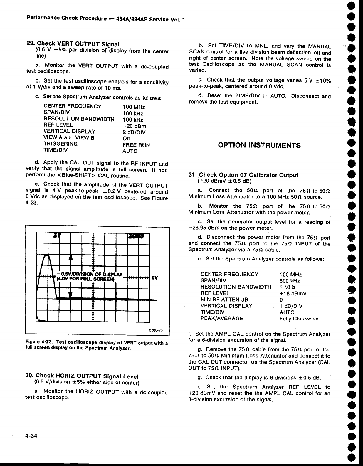
Performance
check
Procedure
- 4g4Al4g4Ap
servrce
Vor.
I
29.
Check
VERT
OUTPUT
Signal
(0.5
V *5% per
division
of disptay
from
the
center
line)
a. Monitor
the VERT
OUTPUT
with a dc_coupted
test oscilloscope.
b. S€t
the
test oscilloscope
controls
for a sensitivity
of 1
V/div
and a sweep
rate
of 10 ms.
c. Set
the
Spectrum
Analyzer
controls
as
follows:
CENTER
FREQUENCY 100
MHz
SPAN/D|V 100
kHz
RESOLUTTON
BANDWTDTH 100
kHz
REF
LEVEL -20dBm
VERTICAL
OISPLAY 2 dB/DIV
VIEW
A and V|EW
B Off
b. Set TIME/D|V
to MNL, and vary the MANUAL
SCAN control
for a five
division
beam
deflection
left
and
right of center
screen. Note
the voltage
swe€p
on the
test Oscilloscope
as the MANUAL
SCAN
control
is
varied.
c. check that the output
voltage
varies
5 v *.10"/o
peak-to-peak,
centered around
0 Vdc,
d. Reset
the TtMEiDtv
to AUTo. Disconnect
and
remove
the
test
equipment.
OPTION INSTRUMENTS
31.
Check Option 07 Calibrator
Output
(+20
dBmV
r0.5 dB)
a. Connect the 50O port of the 75o to 50o
Minimum
Loss
Attenuator
to a 100 MHz
50O source.
b. Monitor the 75o port of the 75o to 50o
Minimum
Loss
Attenuator
with
the
power
mgter.
c. Set the generator
output level
for a reading
of
-28.95 dBm on
the power
meter.
d. Disconnect
the power
meter
from
the 7SO
port
and connect
the 75O port to the 75O INPUT
of the
Spectrum Analyzer
via
a
75O cable.
e. Set the
Spectrum
Analyzer
controls as follows:
d. Apply
the
cAL oUT signat
to the RF
tNpUT
and
verify
that the signal
amplitude
is full screen. lf not,
perform
the <Blue-SHIFT>
CAL
routine.
e. check that the amplitude
of the VERT
ouTpuT
signal is 4 V peak-to-peak
+0.2 V centered
around
0 Vdc
as
disptayed
on
the
test
oscilloscope.
See
Figure
4-23.
Flgure 4-23. Test oscllloscope dlsplay of VERT
output wlth a
full screen dlsplay on the Spectrum Analyrer.
30.
Check
HORIZ
OUTPUT
Signat
Level
(0.5
V/division
*syo either
sid-e
of center)
a. Monitor
the HORIZ
OUTPUT with
a dc_coupted
test oscilloscope.
TRIGGERING
TrME/DlV FREE
RUN
AUTO
CENTER
FREOUENCY
sPAN/DrV
RESOLUTION
BANDWIDTH
REF LEVEL
MIN
RF ATTEN
dB
VERTICAL
DISPLAY
TrME/DlV
PEAK/AVERAGE
100 MHz
500
kHz
1
MHz
+18 dBmV
0
1
dB/DrV
AUTO
Fully
Clockwise
f. Set the AMPL
CAL
control
on
the
Spectrum
Analyzer
for a
O-division excursion
of
the
signal.
g. Remove
the 75O cable
frorn
the
75O port
ot the
75O
to 50O Minimum
Loss Attenuator
and
connect
it
to
the
CAL
OUT
connector
on
the Spectrum
Analyzer
(CAL
OUT
to
75o INPUT).
g. Check
that the
display
is
6 divisions
*0.5 dB.
i. Set the Spectrum Analyzer
REF LEVEL
to
+20 dBmV
and reset
the the AMPL
CAL
control for an
8-division
excursion
of the signal.
at
t
II
[-i3fi
rrttl
'/DIYISP}I OF DISPLAY
.
FORFIL|.SCREEX) {
lltrl OY
4-34
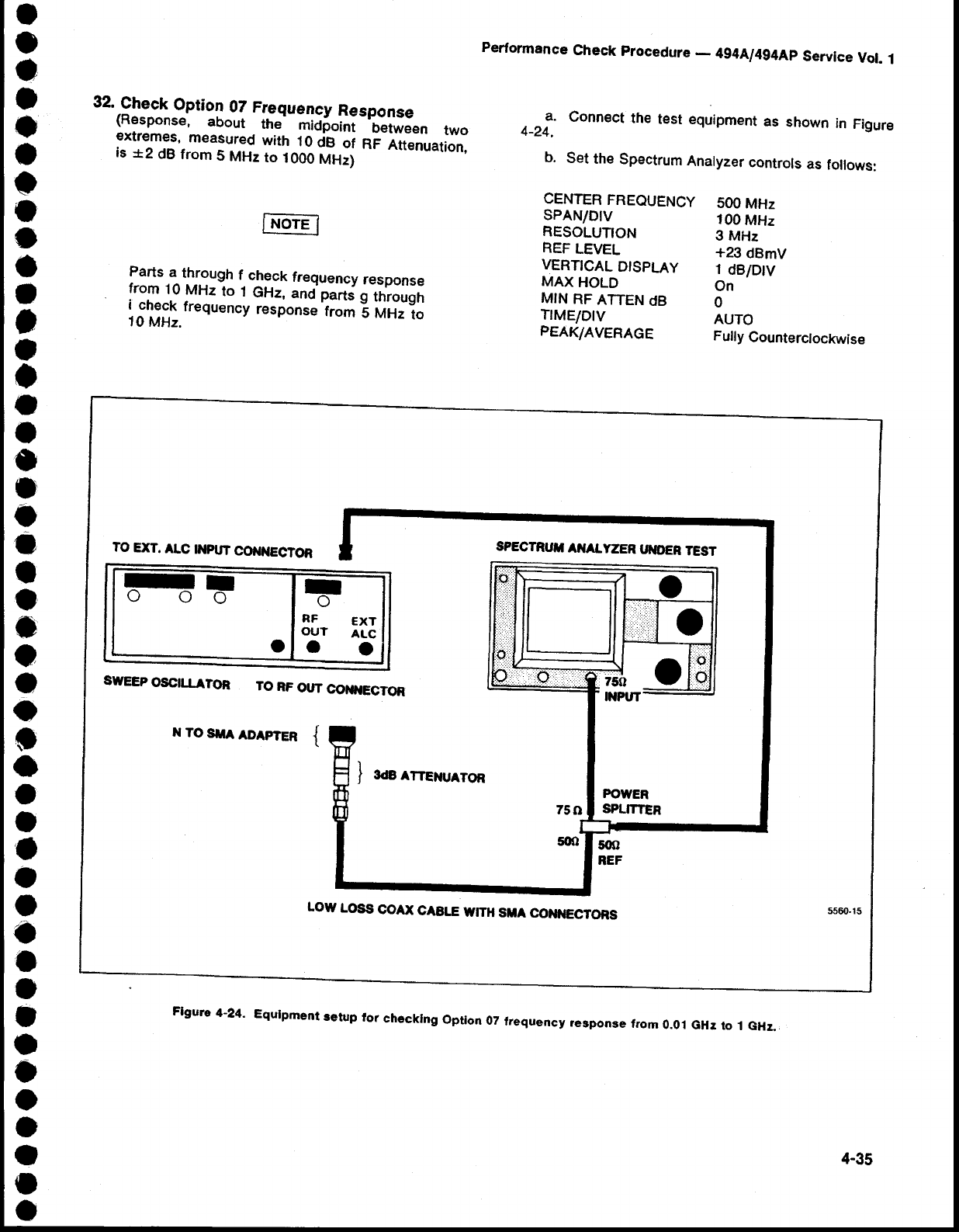
32.Gheck
Option
07
Frequency
Response
(Response,
about
. tt"' rniJioini'.0!i*""n two
€xtremes,
measured
with
10
dg oi nF-ettenuation,
is
*2 dB
from
S
MHz
to
1000
MH;i
farts.lt-trryugh
f check
frequency
response
fro.m
t0 MHz
to 1
GHz,
anO'partJ
g il;;;;
i;ff;:.t*ouency
response
from
6
Mllii"
Performance
Check
procedure
_ 4g4Ll4g4Ap
Service
Vol.
1
a. Connect
the test equipment
as shown
in Figure
4-24.
b. Set
the
Spectrum
Analyzer
controls
as
follows:
CENTER
FREOUENCY
SPANIDIV
RESOLUTION
REF
LEVEL
VERTICAL
DTSPLAY
MAX
HOLD
MIN
RF
ATTEN
dB
TrMElDlv
PEAK/AVERAGE
500
MHz
100
MHz
3 MHz
+23
dBmV
1 dBiDtv
On
0
AUTO
Fully
Counterclockwise
TO EXT.
ALC tilpUTCo0$ttECTOn
Ioo IoIo
RF ExT
OUT ALc
ot ao
SPECTRUII
AiIALYZER
UilOEF
TEST
SWEEP
OSCILLATOR TO RF
OUT
COI{}{ECTOR
r{TOSIIAADAPTER {
POWER
SPLITTER
5G)
REF
LOW
LOSS
COAX
CABTE
WITH
SUA CONilECTORS 5560.15
Flgure 4-24' Equlpment retup for checklng option 0z trequency ?esponse
from 0.ol GHr to 1 GHz.
4-35
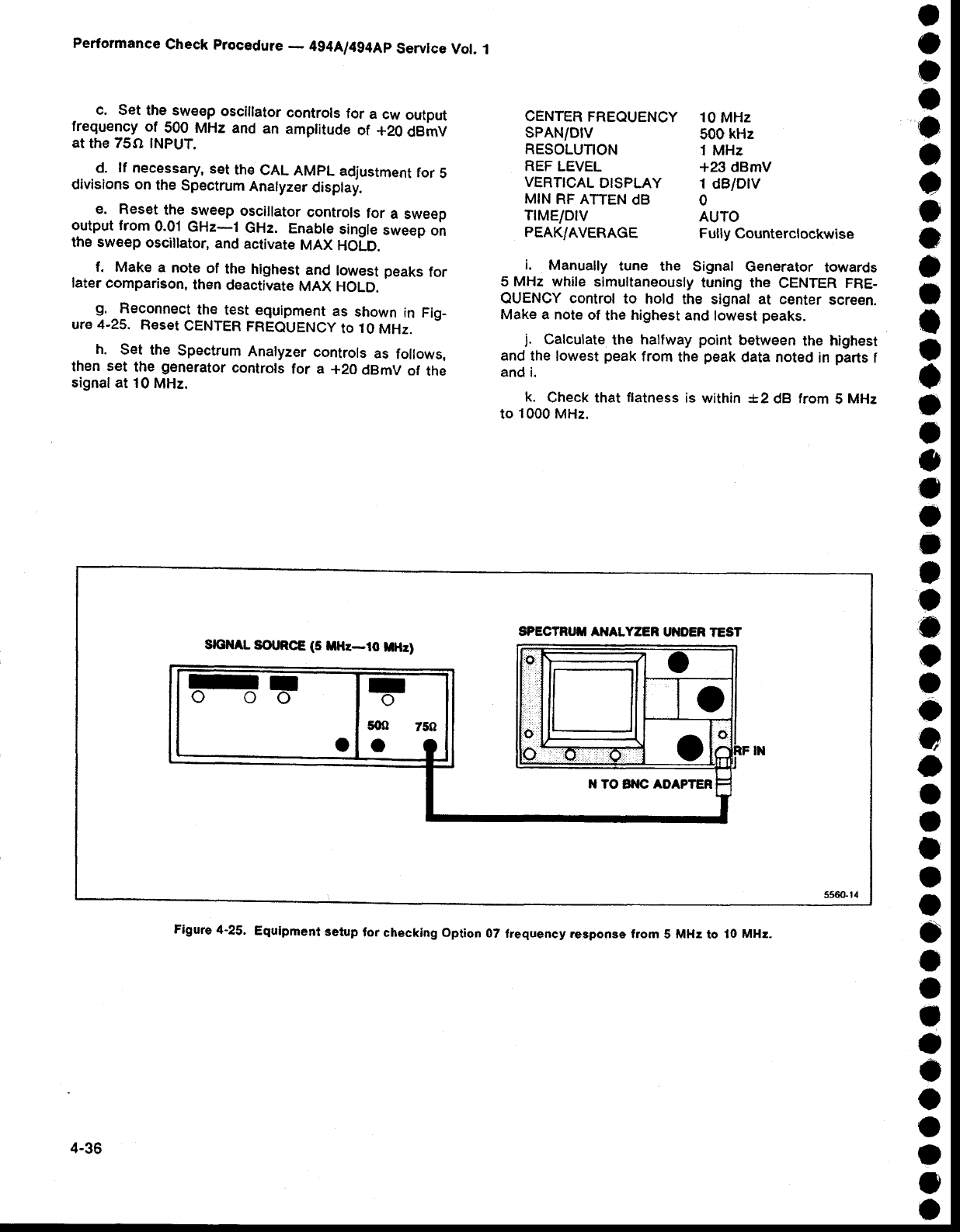
Performance
Check
Procedure
- 4g4A/4g4Ap
Servlce
Vol.
1
- c. Set
tle_:rlveep
oscillator
controls
for a cw output
frequency
of 500
MHz and
an amptitude
of +20
Oe;1V
at
the 75O INPUT.
d. lf necessary,
set
th€
cAL AMPL
adjustment
for 5
divisions on
the
Spectrum
Analyzer
display.
e. Reset
the sweep
oscillator
controls
lor a sweep
output from
0.01 GHz-l GHz. Enable
single
sweep
on
the sweep
oscillator,
and
activate
MAX
HOLD.
f. Make
a note
of the highest
and lowest peaks
for
later
comparison,
then
deactivate
MAX
HOLD.
S, Reconnect
the
test
equipment
as shown
in Fig-
ure
4-25.
Reset
CENTER
FREQUENCy
to 10
MHz.
h. Set the Spectrum
Analyzer
controls
as follows,
then
set the generator
controls
for a +20
dBmV
of the
signal at
10
MHz.
CENTER
FREOUENCY 10
MHz
SPAN/DfV 500
kHz
RESOLUTION 1 MHz
REF
LEVEL +23 dBmV
VERTTCAL
DTSPLAY 1
dBlDlV
MIN
RF ATTEN
dB O
T|MEIDIV AUTO
PEAK/AVERAGE Fully
Counterclockwise
i. Manually
tune the Signal Generator
towards
5 MHz while
simultaneously
tuning the CENTER FRE-
QUENCY
control
to hold the signat at center
screen.
Make a note
of the
highest
and
lowest
peaks.
j. calculate
the halfway
point
between
the highest
and
the lowest
peak
from
the
peak
data noted
in parts
f
and i.
k. Check that
flatness
is
within !2 dB from
5 MHz
to
1000
MHz.
SPECTRUT ANALYZER
UNOER
TEST
Srcl|AL SOT RCE
(5 ltHz-io tdHz]
E!- F
Figure 4-25. Equipment setup for checklng option 07 frequency response from 5 MHz to 10 MHz-
4-36
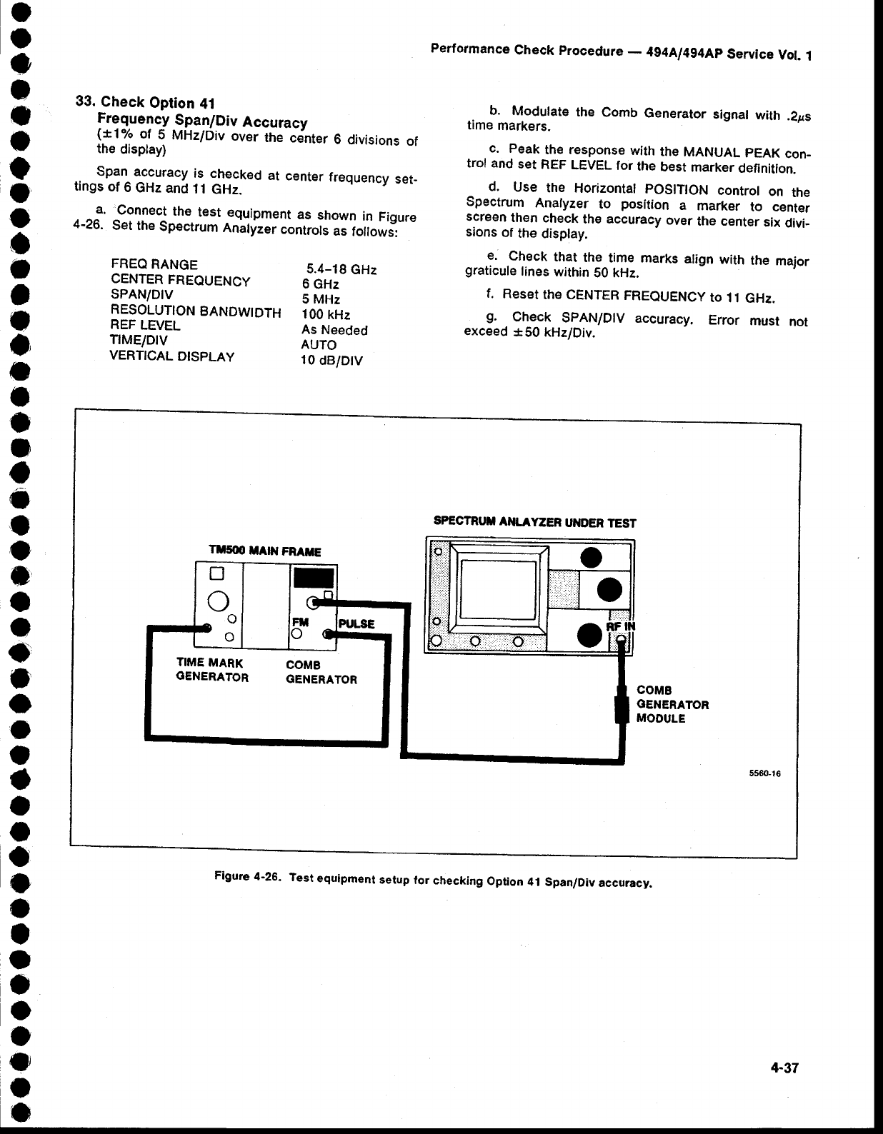
33.
Check Option
4t
Frequency Span/Div Accuracv
!1t73 o.t
5 MHz/Div
over
the
cdnter
6 divisions
of
the
display)
., Sp:laccuracy is c_hecked
at center
frequency
set-
tings
of
6
GHz
and
11
GHz.
a. 'Connect
the test equipment
as shown
in Figure
4-26. set the
sp€ctrum
Analyzer
"ontroir
", follows:
Perforrnance
Check
procedure
- 4g4ful4g4Ap
Service
Vol.
1
b. Modulate
the Comb
Generator
signal
with .2ps
time
markers.
c. peak
the response
with
the
MANUAL
pEAK
con-
trol and
set
REF
LEVEL
for
the
best
marker
definition.
d. use the Horizontal
poslTloN control on the
Spectrum
Anafyzer
to position a marker to center
screen
then
check
the accuracy
over
the center
six
divi-
sions
of the
disptay.
e. Check
that.the^tim€
marks
align
with the maior
graticule
lines
within
S0 kHz.
f. RESET
th€ CENTER
FREQUENCY
tO
11
GHZ.
S. Check SPAN/D|V
accuracy. Error must not
exceed
*50 kHz/Div.
FREQ
RANGE
CENTER
FREQUENCY
sPAN/DtV
RESOLUTION
BANDWIDTH
REF
LEVEL
TrMElDtv
VERTICAL
DISPLAY
5.4-18
GHz
6
GHz
5 MHz
100
kHz
As
Needed
AUTO
10
dB/Dtv
SPECTRUT
ANLAYZER
UIiIDER
TEST
COMB
GENERATOR
MOOULE
Figure
4-26.
Test
equipmeni
setup
for checking
option
4i span/Div
accuracy.
4-37
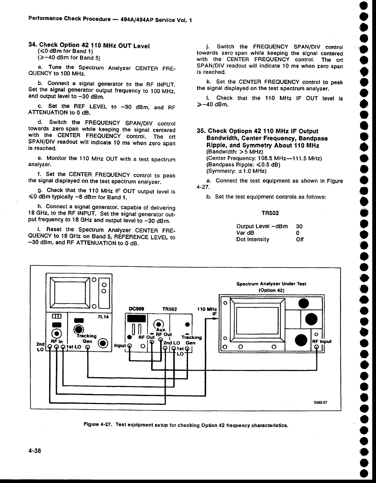
Performance
Check
procedure
- 4g4Al4g4Ap
Service Vol.
1
34.
Check Option 42110 MHz OUT
Level
((0 dBm
for
Band
1)
(>.-40
dBm for
Band
5)
. a. Tune the Spectrum Analyzer CENTER
FRE_
QUENCY
to 100
MHz.
b. Connect
a signal generator
to the RF lNpUT.
Set the
signal
generator
output
frequency
to i00 MHz,
and
output
level
to -30 dBm.
c. Set th€ REF LEVEL to -gO dBm. and RF
ATTENUATION
to O dB.
d. Switch the FREQUENCY
SPAN/D|V control
towards
zero span while keeping
the signal centered
with the CENTER FREQUENCY
controt. The crt
SPANiDIV
readout
will indicate
10 ms when
zero
span
is reached.
e. Monitor
the 110
MHz
OUT with
a test
spectrum
analyzer.
f. set the CENTER
FREOUENCY
controt
to peak
the signal
displayed
on
the
test spectrum
analyzer.
g. check
that
the 110
MHz
tF
ouT output
tevet is
(0 dBm
typically
-8 dBm
for
Band 1.
- h. Connect a signal generator,
capable
of delivering
18
GHz,
to the RF lNpUT.
Set
the
signal generator
out-
put
frequ€ncy
to 18
GHz
and
output
level
to -30 dBm.
i. Reset the Spectrum
Anatyzer
CENTER
FRE-
OUENCY
to 18
GHz
on Band
5,
REFERENCE
LEVEL
to
-30 dBm,
and RF
ATTENUATTON
to 0 ctB.
j. Switch thE FREOUENCY
SPAN/D|V
control
towards zero
span while keeping
the signal
centered
with the CENTER FREQUENCY
control. The crr
SPANIDIV readout
will indicate
10 ms
when
zero span
is reached.
k. set the CENTER
FREQUENCY
controt
to peak
the
signal
displayed
on the
t€st
spectrum
analyzer.
l. check that the 110 MHz tF ouT levet
is
)-40 dBm.
35. Check Optiopn 4211O MHz lF Output
Bandwidth,
Center
Frequency,
Bandpass
Ripple, and Symmetry About 110 MHz
(Bandwidth:
>5 MHz)
(Center
Frequency:
108.5 MHz-l11 .5
MHz)
(Bandpass
Ripple;
<0.5
dB)
(Symmetry:
*1.0 MHz)
a. Connect
the
test equipment
as shown in Figure
4-27.
b. Set the
test
equipment
controls as follows:
TR5O2
Output
Level
-dBm 30
Var
dB 0
Dot Intensity Off
o
o
o
o
I
o
e
o
o
o
o
I
I
o
o
o
o
I
I
o
o
o
o
o
t
o
I
o
o
I
I
O
I
o
o
I
I
o
o
o
o
o
o
o
H:H
ooo
ull
I
e
RF
In
I
O
Trrckiog
Gcn
7L14
o
Spectrsm Analyzer Under Test
(Option 42)
11O
MHz
IF
.Ill
RF
o
Q.
Q 15o'it r'i"line
Input 2ndLO Gcn
4-38
Figure 4-27. Test equlpment setup lor checking option 42 frequency characterlstics.
o
I
o
C
o
t
o
t
o
o
I
)
t
I
C
o
a
o
o
c
o
o
t
a
o
o
o
o
o
o
a
o
a
o
o
o
c
O
o
o
a
o
I
o
7L14
Center
Frequency
Freq
Span/Div
Hz
Resolution
Reference
Level
Display
Mode
Digitaf
Storage
TimelDiv
Triggering
Source
Mode
Video
Filter
110
MHz
1
MHz
3 MHZ
0
dBm
2 dBlDiv
off
Manuaf
Free
Run
Norm
On
Performance
Check
procedure
- 4g4Al4g4Ap
Service
Vol.
1
j. check that the
waveform
symmetry
is *1.0 MHz
(*1.O
division)
by
checking
that the
3 dBpoints
as
wetl
as the 6 dB points on the waveform
are equidistant
from
center
screen.
fl-he
peak
of
the
signal
miy not
Oe
at center
screen).
k. Reset the 7L14 Resolution
Bandwidth to
0.3
MHz,
l. Set the
ZL14
Center
Frequency
control
such
that
the intensified
dot is at
th€
p€ak
of
th; 7L14
disptsr.-'--
m. Check
that the frequency
counter
indicates
a
frequeancy
between
1 t
g.5
MHz
anO
t t
t.S
MHz.
GPIB VERIFICATION
PROGRAM
This verification
program
can
be used
with
a TEK-
TRONIX
4050-Series
Computer
TErminal
to check
the
operation
of the GplB in the Spectrum
Analyzer. All
interface
lines
and interface
messages,
excluding
those
for parallel
poll,
are
verified.
In addition,
the instrument
interface
is checkEd
for
operation
on other primary
addresses,
as well as the
talk-only
and
listen-only
modes.
The
program
is written
in TEKTRONTX
4OSO
BASIC,
and is divided
into individual
tests,
each
for a sp€cific
interface
line,
message,
or function.
The
tests
start
on
even
1000
line numbers
to allow
easy
modification
of
the
program.
The
following
describes
the function
of each
test in
the
program.
Lines
1-5000:
lnterfac€s
to user
definable
keys
for
recovery
from
a failed
test.
Lines
5000-6000:
Inputs
the primary
address
of the
Spectrum
Analyzer
under
test (1
shouldbe
used).
Lines 6000-7000:
tD query response
test. The
instrument
must
be
able
to talk and listen,
to send
out
its lD? response
and manipulate
all eight
of the DIO
lines
for
the
test
to be
successful,
Llnes
7000-8000:
Local
lock-out
test. Tests
correct
operation
of the interface
message
that
should
disable
all
programmable
front-panel
controls.
Lines
8000-9000:
Go to LOCAL
test. Tests
correct
operation
of the interface
message
that should
enable
all
front-panel
controls.
DC
509
Function Frequency
A
chA
Source Ext
Atten X1
Coupl Dc
Opton 42
CENTER
FREQUENCY t10MHz
FREQUENCY
SPAN/D|V 1
MHz
REF
LEVEL _30
dBm
RESOLUTTON
BANDW|DTH 1
MHz
VERTICAL
DISPLAY 2 dB/DIV
MIN
RF
ATTEN
dB O
c. set the 7L14 dot to center
screen
with the
Manual
Scan
control.
d, Set the 7L14
Center
Frequency
controt
for an
indication
of 1j
0.0 on
the f requeniy
Co'unter.
e. swirch the FREQUENcy spAN/DlV control
tgward-s
zero
span while keeping
the signaf
centered
with the oENTER FREOUENCY
contr'ot. The crt
SPANiDIV
readout
will
indicate
10
ms *t"n ."ro "p"n
is reached.
f. set the
7L14
Time/Div
for a catibrated
disptay,
and set the Reference
Level
and
TR502
Var
dB for full
screen
signal.
g. Switch
the TRS02
Dot Intensity
,,on",
and reset
the
7L'l4
Center
Frequency
for
an
indiiation
o,
1
10.0
on
the Frequency
Counter.
h. Check
that the 3dB bandwidth
(1.5
divisions
from
the
peak
of
the
signal)
is )5 MHz.
_^i: th-"-"!_that
any
ripple
present
on the display
is
<0.5
dB
(0.25
divisions
or
tess).
4-39
Performance
Check
procedure
- 4g4A/4g4Ap
Service
Vol.
I
Lines 9000-10000:
Group Execute Trigger test.
Checks
that a GET message
does cause
the Spectrum
Analyzer
to abort the present
sweep
and re-arm
the
trigger, causing
a sweep
to start
and
end,
sending
out
an End-of-Sweep
SRe. Thus,
the SRe line and GET
m€ssage
are
verified.
Lines 10000-11000:
Selected
Device Clear Test.
This
test verifies
that an
SDC message
resets
the
Spec-
trum Analyzer's
GplB output
buffer clearing
out it's lD?
response.
Lines 11000-12000:
Device
ctear
test. This
test is
identical
to the selected
device
clear
test, except
the
universal command
DCL
is used
instead.
Lines 12000-13000:
Addressed
as tistener,
tatker
test. This
t€st checks
that
the microprocessor
correcily
recognizEs
that the GPIA chip has been
addressed
to
listen
or talk, and sends
the appropriate
character
to
the ert readout (L or T).
Lines 13000-14000:
Seriat poil test. This checks
correct
operation
of the serial poll enable (spE) and
serial poll disable (SPD) interface messages. The
status
byte is read,
and if anything
other
than
ordinary
operation is indicated,
the instrument
tails
the
test.
Lines
14000-15000:
GptB rear
panet
switch
test. Atl
five primary
address
switch€s
are checked
for corr€ct
operation.
Three
subroutines
are
called
in the process
of testing
one
address
switch. The
first
two send
a for-
matted
rnessage
to the 4050
display,
and
the
third
per-
forms
the
address
switch
test.
Lines 1500G16000:
Line feed or EOt switch test.
Checks
for correct
selectlon
of line
feed
as a termina_
tion when selected
by
this switch
by
sending
an
lD?
ter_
minaled only
by a line
feed.
Lines 16000-17000:
Talk-only mode t€st. When
selected,
this mode should cause the instrument
to
send a SET? response
and (optionally)
a CURVE?
response whenever
the RESET-TO-LOCAL
button is
pressed. The string received
from the instrument
is
thus
examined
for existence of a portion
of the correct'
SET?
response
after the RESET-TO-LOCAL
button
is
pressed.
Lines 17000-18000:
Listen-only
mod€
test. When
selected, this mode will cause ths instrum€nt
to
respond to any message
on the bus, since
it is always
addressed
to listen. The command
REF
0 is sent
to the
bus without addressing
the instrument,
then the listen-
only mode is deselected
and the instrument interro-
gated to see if it did respond
to the REF command
while
in
the
listen-only
mode.
Lines 18000-'19000:
Interface clean (and Remote
Enable) test. This
IFC line
on the
GPIB will
unaddress
the
instrument's
interface. This is
verified
by
noting
that
the L is not present
in the crt readout,
indicating
that
the IFC line worked; also the REN line will be
unasserted
when
the
end statement is executed
(except
for some
early
4052 and 4054's).
Thus, a front
panel
in
the local
mode indicates
that the REN
line was
success-
fully
unasserted.
(Evidence
it was asserted
is that
the
instrument
was able
to execut€ commands
sent
to it by
previous
tests.)
Lines 19000-end:
Utility
routines. Rear
panel
inter-
face switch
test text routine
puts headers
on the inter-
face switch
test display.
The rear panel
test text rou-
tine tells the operator
what to do after changing
the
address switches.
Test
address
switch
acquires an lD?
response from
the
instrum€nt on its
new address during
the address switch
test. The
SRQ
handler
will handle
SRQ's
that occur, although
none would be expected,
except the power-up
SRO. (fhe end of sweep
SRQ
during the GET test is handled by anoth€r SRQ
handler.) Delay
Generator
generates
delays
lor other
tests. The
Failure Decision Handler
allows
the
program
to be restarted
with the user-definable
keys if any
test
fails.
o
t
o
o
t
o
t
o
o
o
I
I
I
t
o
a
o
o
I
t
o
a
o
a
I
o
o
o
o
o
I
o
o
o
o
o
o
o
o
o
a
o
t
I
1
GOTO s000
4 B2-1
5 RETURN
20 B2-5
21
RETURN
5OOO
REM
"'49XP GPIB
VERIFICATION
PROGRAM
'-'
5030 tNlT
5O4O
ON SRQ THEN
19280
5050
DrM V$(400),w$(400)
506017-0
5O7O PAGE
5080
pRtNT'J.JJENTER
49Xp'S
pRlMARy
ADDRESS
(DEFAULT:
1)
";
5O9O INPUT T$
5100 tF TS<>" THEN
5130
5110 A1-1
s120
GO
TO
5180
4-40
o
o
o
o
a
o
t
t
o
o
o
o
t
a
I
I
o
o
o
o
o
o
t
I
a
o
t
o
I
o
o
o
o
a
o
a
o
r
C
o
o
o
I
o
Performance
check procedure
- 4g4A/4g4Ap
service
vor.
1
5130 A1-vALrr$)
5140 tF
A1>0
AND
A1
<31
THEN
5180
:1i9lllltl "{JJGERROR!!
';A1;,
tS
Nor A vALtD
ADDRESS,,;
5160
PRINT
"
ONLY
O THRU
gO
INE VALID
ADDRESSESKK'
s170
co To 5080
5180 PAGE
5190
REM
52OO
REM
5210
REM
5220
REM
5230 REM
6000
REM
rrr'IDr
QUERY
RESPONSE'-'
601 O PRINT
'r.i '(IDOI'
OUERY
RESPONSE
..".
6020
PRTNT
@A1
:"tNlT;lD?;SlG,,
6030INPUT
@A1:T$
6040
v$-sEGCr$,1,9)
6050!F
V$:"lD
TEK/49'THEN
60g0
9999 lltryI'J,Jf.""tD,, QUERY
RESPONSE
.r. FA|L
-rcil
6070
GO TO
19s30
6080
WBYTE
@32+A1
:64,1
28,-1
ZZ
6090
PRINT
@A1:,WFM
ENC:B|N;CUR?.
61 00 PRINT
@37,0:07,255,255
6110INPUT
o/"A1:Tg
6120
WBYTE
@6a+A1:
6130 RBYTE
R,R,R,T6
6140
WBYTE
@95:
6150 lF
R->128
AND
T6<128
THEN
7O0O
61
60
PRINT'JJ
J...
Dlog
TEST
..' FAIL,*G"
6170
co To 19530
6180
REM
6190
REM
6200
REM
6210
REM
6220 REM
7000
REM
.'r LOCAL
LOCK-OUT..............LLO
".
7010
PRINT
""' LOCAL
LOCK-OUT..........LLo
.,."
7020
WBYTE
@32+A1,17:
7030
PRINT
@A1:,.SET?"
7040INPUT
@At:V$
19!g l!!NI "Ll4exp
tN
LocAL
LocK-our
MoDE
(LLo)"
lggg lllNr tLArrEMpr
ro usE
4exp
coNrRoLs"
1g1g ryNr.'!_!_PRESS
RETURN
<CR>
WHEN
DONE,';
7O8O
INPUT
T$
7090
PRINT
@A1:"SET?,'
7100INPUT
@At:W$
7110
tF
W$<>v$
THEN
7130
7120
cO TO
8000
7130
pntNT'!". LOCAL
LOCK_OUT.............LLO
'., FAtL
..G,'
7140
cO TO
19530
7150
REM
7160
REM
7170
REM
7180
REM
7190
REM
8000
REM
*.'GO
TO
LOCAL.............GTL'..
801
0
PRINT
@Al
:"lNtT;TtM?"
8020INPUT
@A1:R
8030
PRINT
@A1:"TtM
tNC.,
8040
pRtNT
*.r co To LocAL.............GTL
.'."
8050 WBYTE
@32+41,1:
4-4'l
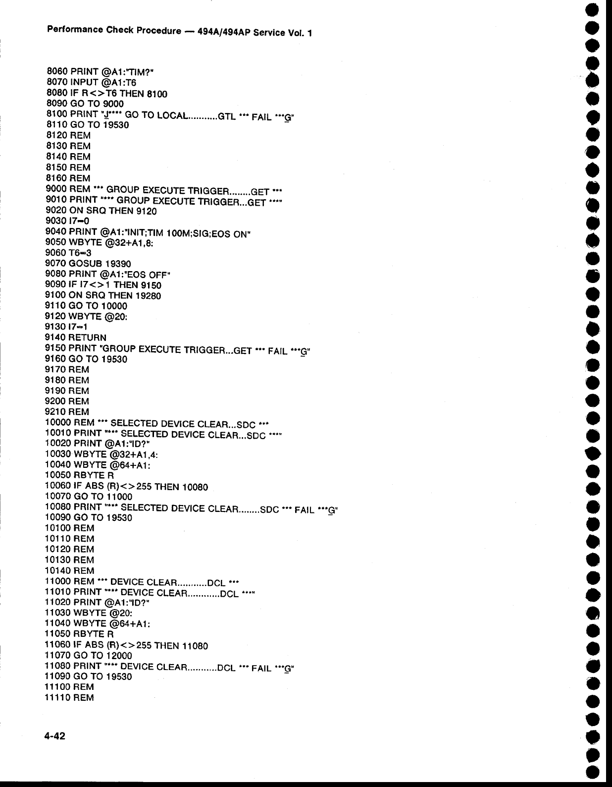
Performance
Check
procedure
- 4g4Ll4g4Ap
Service
Vol.
1
8060
PRINT
@A1:'TlM?,
8070INPUT
@41:T6
8080
tF R<>T6 THEN
8100
8090
GO TO
9000
8100 PRINT
"J".. GO TO
LOCAL...........GTL
'* FAIL
*rG,
8110
cO TO 19530
8120
REM
8130
REM
8140
REM
8150
REM
8160
REM
9OOO
REM
"' GROUP
EXECUTE
TRIGGER........GET'*'
9O1O PRINT
"''' GROUP
EXECUTE
TRIGGER...GET
"TS
9O2O
ON
SRQ
THEN
9120
9030 r7-0
9040
PRTNT
@A1:"]NlT;TtM
10OM;S|G;EOS
ON"
9050 WBYTE
@32+41,8:
9060
T6-3
9070
cosuB 19390
9080 PRINT
@A1:"EOS
OFF',
9090 rF 17<>'t
THEN
9150
91OO
ON
SRQ
THEN
19280
9110
GO TO
10000
9120
WBYTE
@20:
9130l7*1
9140
RETURN
9150 PRINT "GROUP
EXECUTE
TRIGGER...G
9160
cO TO 19530
9170
REM
9't
80 REM
91
90
REM
92OO REM
9210
REM
lOOOO
REM'" SELECTED
DEVICE
CLEAR...SDC
..'
1OO1O
PRINT
""' SELECTED
DEVICE
CLEAR...SDC
-""
10020
PRINT
@A1:'tD?"
10030
WBYTE
@32+A1,4:
10040
WBYTE
@64+A1:
lOO5O
RBYTE
R
10060
tF
ABS
(R)<>2s5
THEN
10080
10070
coTo 11000
10090
pRtNT
"...
SELECTED
DEVICE
CLEAR........SDC
*r FAtL
.'.G'
10090
Go To 19530
10100
REM
10't10
REM
1
01 20 REM
10130
REM
10140
REM
11000
REM
.'. DEVICE
CLEAR...........DCL.'.
11010
pRtNT
"...
DEVTCE
CLEAR,...........DCL
..'"
11020
PRINT
@A1:"lD?'
11030
WBYTE
@20:
11040
WBYTE
@621+A1:
1
1
O5O RBYTE
R
11060 rF
ABS
(R)<>255
THEN
11080
11070
GO TO
12000
11080
pRINT
.'."
DEVICE
CLEAR...........DCL
11090
GO TO
19530
11100
REM
11110
REM
4-42
o
o
o
I
a
a
t
o
o
o
o
o
o
o
o
o
o
o
t
o
o
o
o
o
I
o
o
o
C
t
o
o
a
t
o
I
a
o
o
a
a
I
)
o
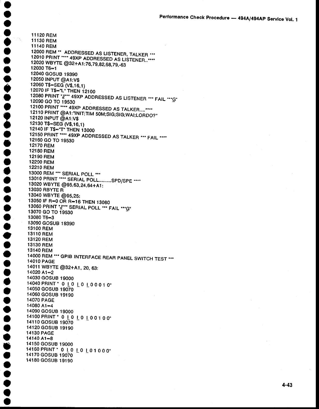
t
O
o
I
o
o
?
o
o
c
o
o
I
)
o
T
o
t
o
a
o
o
o
o
o
e
a
o
o
o
o
e
o
o
)
t
o
o
a
o
o
I
a
I
perrormance
check procedure
- 4g4A/4g4Ap
servrce
vor.
1
11120
REM
11130
REM
1 I
140
REM
12OOO
REM
" ADDRESSED
AS
LISTENER,
TALKER
"'
1 201
0
pRtNT,...
49xp
ADDRESSEb-
ndlisreneR...*tr
I ?9?9 I/-BvTE
@32+Al
:
76.zg,se,6s,id,-eJ
12030
T6-1
12040
cosuB 19390
12050INPUT
@A1:vg
1 ?ggg
r_$*gEG
(v$,1
6,1
)
12070
tF
T$:"L,'
THEN
i21
0o
12080
PR]NT
"J'"'49XP
ADDRESSED
AS
LISTENER
Jr'
FAIL
"iGS
12090
cO TO
19530
12100
pRtNT
"'.*
4gxp
ADDRESSED
AS
TALKER......_,
] ?1 I n|!] @A1
:',t
Ntr;TM
soM;stc;sf
d,wel,r_onooz"
12120INPUT
@A1:V$
1?139
r$-sEG
(v$,16,1)
121
40
tF
T$-"T"
THEN
i3ooo
12150
PRINT
O"'49XP
ADDRESSED
AS
TALKER
rA.
FAIL
.irtr
12160
cO TO
19530
12170
REM
12180
REM
12190
REM
12200
REM
't2210
FEM
13OOO
REM
*" SERIAL
POLL
*..
13010
pRtNT'.".
sERtAL
poLL.........spD/spE
*rr
1
3020
WBYTE
G)95,63,
24,64+4l
:
13030
RBYTE
R
13040
WBYTE
@95.25:
13050lF
R-0
OR R-l6 THEN
.t3080
lgggq tltryT'J."
SERTAL
POLL...
FAIL
*..cn
13070
GO TO
19530
13080
T6:3
13090
cosuB 19390
13100
REM
13110
REM
13120
REM
13130
REM
13140
REM
14OOO
REM
"'GPIB TNTERFACE
REAR
PANEL
SWITCH
TEST
"'
14010
PAGE
14011
WBYTE
@32+A1,
20.
63:
14020
A1*2
14030
GOSUB
19000
14040PR|NT'
0 !_0
L0 !_00010"
14050
cosuB 19070
14060
GOSUB
19190
14070
PAGE
't4080
A1-a
14090
cosuB 19000
14100PR|NT"
0 !_0
!_o
L00100,
141 10
GOSUB
.t
9070
14120
GOSUB
19190
14130
PAGE
14140
A1:8
141s0
cosuB 19000
14160PRINT"
0 !_0
!_o
!_01000,
14170
GOSUB
19070
14180
GOSUB
19190
4-43

Performance
Check
procedure
_ 4g4Ll4g4Ap
Service
Vol.
1
14190
PAGE
14200
A1-16
14210
GOSUB
19000
14220PR|NT"
0 L0l0 l_1o0oo.
14230
GOSUB
19070
14240
GOSUB
19190
14250
REM
14260
REM
14270
REM
14280
REM
14290
REM
15000
REM
., nLFr
oR ,EOl.
swlTcH .,"
15010
PAGE
15020
41:1
15030
cosuB 19000
15040PR|NT.
0 to L 1 !_0OOO1"
1s050
GosuB 19070
15060
PRINT
"JJTESTTNG "EOt''SwtTcH"
15070
cosuB 19190
1
5080 WBYTE
@32+A1
:73,68,63,1
0
15090INPUT
@A1:T$
1
51 00 r$-sEG cr$,1
,9)
15110lF
T$-"lD
TEK/49,
THEN
15140
1
51 20 PRINT
U*LF"
.OR'
uEOl"'swlTcH
15130
GO
TO
19530
1
51
40
T6-2
15150
GOSUB
19390
15160
REM
15170
REM
15180
REM
15190
REM
15200
REM
16000
REM
'" TALK
ONLY
MODE
""
16010
PAGE
16020
cosuB 19000
16030PR|NT"
0 !_
1 !_0
!_oooo1'
16040
cosuB 19070
16050
PRTNT
!{JTEST|NG
TALK
ONLY"
16060INPUT
@A1:V$
16070
I7-POS (V$,"rrNe
oFF",l)
160801F
t7<>0 THEN
17000
16090
PRINT
''JJJTALK
ONLY
MODE
O"
FAIL
rr'GT
16100
co To 19530
16110
REM
16120
REM
16130
REM
16140
REM
16150
REM
17OOO
REM
'" LISTEN
ONLY
MODE
"'
17010
PAGE
17020
GOSUB
19000
17030PR|NT'
1!_
0!_
0 !_00001"
17040
cosuB 19070
17050
pRtNT
"JJJTESTTNG
LISTEN
ONLY"
17060
PRINT
@A1:"tNt',
17070
T6-0.5
17080
GOSUB
19390
1 7090
WBYTE
92,69,70,32,_48
17100
PAGE
17110
GOSUB
19000
4-44
o
O
o
t
o
o
o
o
c
c
o
t
?
o
o
I
o
t
I
I
o
o
o
o
I
o
o
o
o
I
o
a
o
o
a
o
o
a
I
o
o
o
,
O
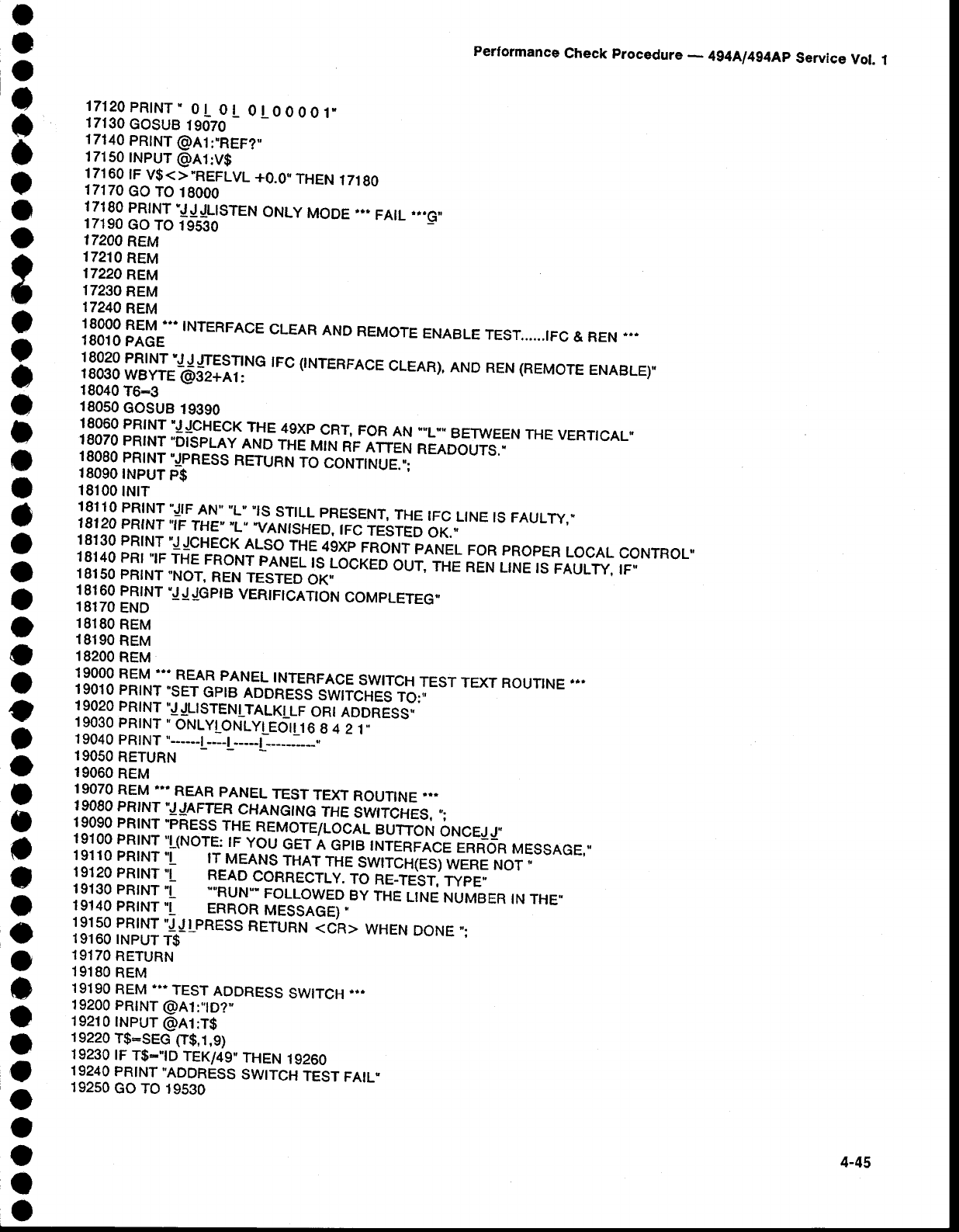
I
o
o
C
o
a
I
I
o
e
C
o
o
a
o
;
o
I
a
o
o
a
o
o
o
e
o
O
t
o
o
C
o
o
o
o
o
o
o
o
a
)
o
o
performance
check procedure
- 4g4Ar4g4Ap
servrce
vor.
1
17120
PR|NT'
0L ol_
0LO
OOO
I,
17130
cosuB 19d70
1
7140
PRTNT
@A1
:'REF?,,
17150INPUT
@At:V$
17160
tF
v$<>"REFLVL
+0.0.
THEN
17180
17170
co To 18000
11199lltu IJ{L|SrEN ONLY
MODE
'r. FA|L
*.Gn
17190
co To 19530
17200
REM
17210
REM
17220
REM
17230
REM
17240
REM
'8OOO
REM
"'INTERFACE
CLEAR
AND
REMOTE
ENABLE
TEST......IFC
& REN
','
18010
PAGE
13333
fiBlI.6gilT:-" rFc
(TNTERFACE
CLEAR),
AND
REN (REMorE
ENABLE)"
18040
T6-3
180s0
GosuB
19390
l!999llfNr lJcHEgK-rHE
4exp
cRr, FOR BETWEEN
rHE
vERflCAL"
18070
PRTNT
"OISPLAY
AND
THE
r"Iirr
N'E
ATTEN
READOUTS."
18080
pRtNT
"JPRESS
RETURN
rO Corvrir.ruE.,;
18090INPUT
P$
18100
tNtT
18110
PRINT
UF AN"
"L"
"IS
STILL
PRESENT,
THE
IFC
LINE
IS FAULW,,
18120
pRtNT'lF
THE"
"L"
"VAN|SHID,'tr-crEsreo
ox."
18130
PRINT
lJcHEc^K
ALSO
THE4bip
raor'rr pANaL
FoR
pRopER
LocAL
coNTRoL'
18140
PRI
'lF
THE
FRONT
PANEL
rS
iOcxeo ouT,
THa
nir.t
r_rivE
ts FAUL,",
tF,
18150
PRINT
"NOT,
REN
TESTED
OK;- --'
]9199 nryr !J{GPIB
vERlFlcArtoH
cotapr-erEo"
18170
END
18180
REM
18190
REM
18200
REM
19OOO
REM
*'REAR P4NEL
INTERFACE
SWITCH
TEST
TEXT
ROUTTNE
"'
19010
PRINT
"SET
GPIB
ADDRES'
SWIiCTTES
rO,.
199?9 fllNr "JJLrsrEN!_TALKTLF
oCr noiness"
19030
pRtNT
. ONLy!_ONLy!_Eor!_ro
s q 2 l"
1
9040
pRtNT
*---t ---l ----t ___--------
19050
RETURN
19060
REM
19070
REM
''' REAR
PANEL
TEST
TEXT
ROUTINE
"'
1?gg? llfNr IJAFTER
CHANGING
rHE
swrrcHEs,
,;
19090
PRINT
"PRESS
THE
REMOTCIUObIi
BUTTON
ONCEJJ.
lglgg lllNr "r-(NorE:
rF
you
eer i eiia rNieRiobE
L"#o=n
MESSAGE,"
19110
PRINT
,'!_ trI4EANS
*rer rr_re
swrrcH6Sl
WERE
Nbi
"
19120
PR]NT
-!- READ
CORRECTLY.IO
RE-TEST,
TYPE"
19130
PRINT
1 rouowEo ei rHe LINE
NUMBER
IN THE"
19140
PRTNT'!_ ERROR
MESSAGE)'
19119 IINI lJ!_pREss
RETURN
<ch> WHEN
DoNE
";
19160
INPUT
T$
19170
RETURN
19180
REM
19190
REM "'-
TEST
ADDRESS
SWITCH
"'
19200
PRINT
@At:,,1D?"
19210INPUT
@A1:T$
19220
T$:SEG
Cr$,1,9)
19230
tF
T$-,lD TEK/49"
THEN
19260
19240
PRINT'ADDRESS
SWITCH
TEST
FAIL"
19250
cO TO
19530
4-45
Performance
Check procedure
_ 4g4Ll4g4Ap
Servlce
Vot.
1
19260
RETURN
19270
REM
19280
REM
". SRQ
HANDLER
".
19290
T6-3
19300
cosuB
19390
19310
POLL
21,21;A1
19320
PRINT
@A1:"ERR?"
19330INPUT
@A1:S$
19919 !l!NT "GGAN
TNTERRUPT
occuRRED
oN
rHE
BUs,
rHE
4exp
RETURNS ";s$
19350
pRtNT
"JPRESS
RETURN
<CR> TO
CONTTNUE';
19360INPUT
T$
19370
RETURN
19380
REM
19390
REM
"'DELAY GENERATOR
-'
19410
REM
... T6
GTVEN
tN
SEC
(GLOBAL)
**.
tg
scRATcH
...
19420
tF
T6<0 THEN
19510
19430
tF
RND
(0)>0.5
THEN
19490
19440
REM
... 4051
*r
19450
T6-T6'220
19460
FOR t9-1 TO
T6
19470
NEXT
t9
19480
GO TO
19510
19490
REM
'..4052
19500
CALL
"WA!T..T6
19510
T6-0
19520
RETURN
19530
REM
"'' FAILURE
DECISION
HANDLER
.',-
19540
PRINT
!{SELECT A UDK:'
19550
PRTNT
"!_ (1)
RE-START'
19560
PRTNT
"L (5)
END"
19570
SET KEY
1
9580
B2-0
19590
tF B2<>1 AND
B2<>5 THEN
19590
19600
lF B2-5 THEN
19630
19610
PAGE
1
9620
cO TO 6000
19630
END
o
a
o
t
o
a
o
o
o
?
c
o
o
o
o
a
o
o
o
I
a
O
o
o
o
o
o
o
o
o
o
I
o
o
o
o
o
o
o
o
o
o
,
o
4-46
ADJUSTMENT
fntroduction
l{
the lnstrument
performance
is not
within
specified
requarements
for a particular
characteristic,
determine
the
cause,
repair
if necessary,
then
use
the
appropriate
adiustment
procedure
to retuln the instrument
operation
to .performance
specification.
After any adjustment,
verify performance
by repeating
that part;f the perfor_
mance
Check.
Allow the instrum€nt
to warm up for at least
one
hour,
in an ambient
temperature
of *20" C to +30o
C
FI:* m.aking
any
adjustments.
Waveform
iilustrations
tn tne adrustment
procedure
are typical
and may
differ
from one instrument to another: These waveforms
should not b€ construed
as being repres€ntative
of
specift
cation
tolerances.
o
o
a
o
I
o
o
t
o
o
o
o
o
o
o
o
a
o
a
o
o
o
O
O
o
o
o
o
o
o
a
o
t
o
o
a
o
o
o
o
o
o
o
O
Secdon
5 - 4g4Al494Ap
Service
Vot.
1
STANC
DISCHARGE
CAN
DAMAGE
MANY
SEMICONDUCTOR
COMPONENTS
USED
IN
THIS
INSTRUMENT.
Many semiconductor
components,
esDe-
cially
MOS
types,
can
be damaged
Oy stitic
discharge. Damage may not be catas-
trophic and, therefore, not immediately
appare-nt.
lt usually
appears
as a degrada-
ilon or the semiconductor
characteristics.
Devices-lhat are particularly
susceptible
are: MOS, CMOS, JFETa, and high
impedance
operational
amplifiers
(FET
inp-ut
stag€s.) The damaged
parts may operate
wttntn
accepted
limits
over a short
period,
but their reliability
wiil have
been
severely
impaired.- Damage can be significanily
reduced
by observing
the following
p.ecau-
tions.
1. Handle
static-sensitive
components
or
circuit
assemblies
at or on a static-free
sur_
face. Work station
areas
should
contain
a
static-free
bench
cover or work plane
such
as conductive
polyethylene
sheeting
and a
grounding
wrist strap. The work plane
should
be connected
to earth
ground.
2. All test equipment,
accessories,
and
soldering tools should be connected
to
earth
ground.
3. Minimize
handling
by keeping
the com_
ponents in their original containers
until
ready
for use. Minimize
the removal
and
installation
of semiconductors
from
their cir_
cuit
boards.
4. Hold
the lC devices
by their
body
rather
than
the
terminals.
5. Use containers
made of conductive
material
or filled with conductive
materiat
for storage
and
transportation.
Avoid
using
ordinary
plastic
containers.
Any static
sen_
sitive
part
or assembly
(circult
board)
that is
to be returned
to Tektronix,
lnc.,
should
be
packaged
in its original
container
or one
with
anti-static
packaging
material.
Equipment Required
Table 5-1 lists additional
test equipm€nt
and test
fixtures recommended
for the adjustment
procedure.
Test equipment
list€d
in Table
5-1 together
with those
listed
in Table
4-1
in Section
4, performance
Check are
required
for the adjustment
procedure.
The characteris_
tics specified
are
the minimum required
for the
checks.
Substitute equipment must meet or exceed these
charact€ristics.
5-1
Adluctment
Procedure
- 4g4A/4g4Ap
Servtce Vot.
1
o
o
o
o
o
o
o
)
o
o
o
o
o
o
;
a
o
o
I
I
o
O
o
o
t
o
o
O
o
o
a
o
)
o
o
o
t
o
I
o
a
a
a
o
Table 5-l
EOUIPMENT
REOUIRED
Equlpment
or Test
Flxture
lsolation
Transformer
Att€nuator (3
dB miniature)
Autotransformer
Multimeter
Dc
Block
Adapt€r
(Sealectro
male
to male)
Adapter (bnc female to Sealectro
male)
Three Extension
Cables (Sealectro
female
to Seal€ctro
male)
Adapter
(bnc
to Sealectro)
Adapter
(bnc
female
to sma
male)
Cable
(20"),
Tip
Ptugs
to bnc
CoaxialCable
(8)
50 O Terminator
Screwdriver,
Tuning
Alignment
Tool
Screwdriver, Flat,
6" with
1/8,
Tip
Screwdriver,
Phillips
No.
1
Recommendatlon
and
Use
Stancor
G|S21000
Weinchel
Model 4M, Tektronix
Part
No.
015-1053-00
General
Radio Variac Type
Wl0MT3
TEKTRONIX
DM 5O1A
or DM 5O2A
Tektronix
Part No.
015-022140
Tektronix
Part 1
0i!-0098-00
Tektronix
Part No. 103-0180-00
Tektronix
Part No. 17$2902-00
Tektronix
Part No. 175-241240
Tektronix
Part No. 015-1018-00
Tektronix Part
No.
175-1178-00
Tektronix
Part No. 012-020&00
Tektronix
Part No.
011-0049-01
Tektronix Part
No. 003-0675-00
Tektronix Part No. 003-0968-00
Tektronix Part No. 672-0865-01
4. Place
the instrument
on the bench
and reconnect
the power
cord.
Some circuit boards or assemblies must be
removed
and placed
on extenders
to gain access
to
some test points
or adjustments.
When this is done,
turn the
power
off
before
removing
the
assembly.
Allen Wrenches (3), 3lgl, 5/il"
7lu
Service
Kit
(Extender
Boardsla
1:1
turns ratio
AND
AT
LEAST
500
VA
Frequency,
to 5 GHz;
connectors
5 mm
Capable
of varying
line
vottage from 90
Vac
to 130
Vac
100
pV
to 350
Vdc
ADJUSTMENT
PROCEDURE
PREPARATION
Remove
the cabinet
as
follows:
1. Set the
instrument
on its
face
or front
panel.
2. Loosen
the lour screws
through
the back rubber
feet.
3. Pull
the cover
up and
off.
e This kit is pari of the service Kit 006-3286-01.
listed in the Maintenance section,
5-2
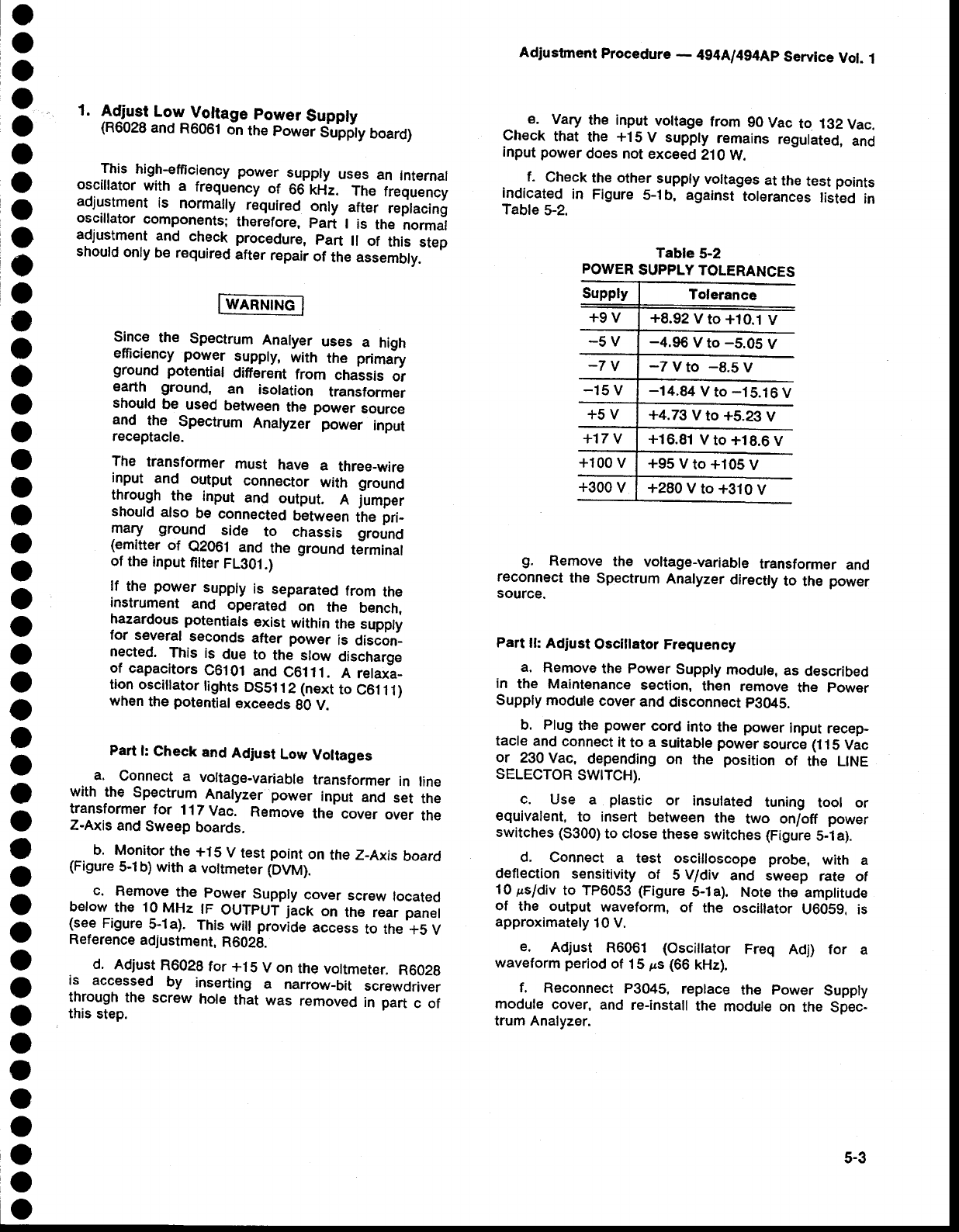
o
o
o
o
o
o
o
o
o
o
o
a
o
o
o
o
o
O
o
o
o
o
o
o
o
o
,
o
o
o
a
o
o
o
a
o
O
o
o
o
o
o
o
o
1. !{iust Low
Vottage
power
Suppty
(R6028
and
R6061
on
the
power
Su'pljly
board)
This high-efficiency
power supply
uses
an internal
oscillator
with a frequency
of 66
i<fiz. The frequency
adjustment
is normally
-required
only after replacin!
oscillator
components;
therefore,
pari t is the normal
adjustment
and check
procedure,
part ll of this step
should
only
be required
after
repair
of the assembly.
Since
the Spectrum
Analyer
uses a high
efficiency
power supply,
with the primjry
ground
potential
different
from chassis
oi
earth ground, an isolation transform€r
should
be used between
the power source
and the Spectrum
Analyzer power input
receptacle.
The transformer
must have a three-wire
input and output connector
with ground
throug.h
the input and output. n tumper
should
also be connected
between
itre
pri-
mary ground side to chassis qround
(emitter
of e2061 and the ground
terminal
of
the
input
fitter
FL301.)
lf the power supply
is separated
from the
instrument
and operated on the bench,
hazardous
potentials
exist
within
the
supply
for several
seconds
after power is discon_
nected.
This is due to the slow discharge
of capacitors
C6101
and
C6111.
A retaxl_
tion osciilator
tights
Ds5112
(next
to
c6111)
when
the
potential
exceeds
g0
V.
Part
l: Check
and
Adjust
Low
Voltages
a. Connect
a voltage-variable
transformer
in ,ine
with the Spectrum
Analyzer
power input and set the
transformer
for l17Vac. Remove
the cover
over
the
Z-Axis
and
Sweep
boards.
b. Monitor
the
+15
V test
point
on the
Z_Axis
board
(Figure
5-1b)
with
a vottmeter
(DVM).
c. Remove
the power
Supply
cover
screw
located
below
the '10
MHz lF OUTPUT
jack on the rear
panel
(see
Figure
5-1a). This
wilt
provide
access
to the
+5 V
Reference
adjustment,
R6O2g.
d. Adjust
R6028
for +15
V on
the
vottmeter.
R602g
is accessed
by inserting a narrow_bit
screwdriver
through
the screw hole
that was removed
in part
c of
this
step.
Adjustment
Procedure
- 494A/4g4Ap
Service
Vol.
1
^ e. Vary
the input
voltage
from 90
Vac
to 132
Vac.
Check that the +1S
V supply
remains
regulated,
and
input
power
does not
exceed
210
W.
f. Check
the other
supply
voltages
at
the
test
points
indicated
in Figure
5-.1b, against
tolerances
lisied in
Table
5-2.
Table 5-2
POWER
SUPPLY
TOLERANCES
S. Remove
the voltage-variable
transformer
and
reconnect
the Spectrum Analyzer
directly
to the power
source.
Part
lt Adjust
Oscillator
Frequency
a, Remove
the
power
Supply
module,
as described
in the Maintenance
section,
then remove
the power
Supply module
cover
and
disconnect
pg045.
b. Plug
the
power
cord into
the power
input
recep_
tacle
and
connect
it to a suitable
power
source
(1
1S
Vac
or 230
Vac, depending
on the position
of the L|NE
SELECTOR
SWTTCH).
c. Use a plastic or insulated
tuning tool or
equivalent,
to insert between
the two on/off power
switches (3300)
to close
these switches
(Figure
5-1a).
d, Connect a test oscilloscope
probe, with a
deflection
sensitivity
of 5 V/div and sweep rate of
10ps/div
to TP6053 (Figure
5-1a).
Note
th€ amplitude
of the output waveform,
of the oscillator
U60S9, is
approximately
10 V,
e. Adjust R6061 {Osciilator Freq Adj) for a
waveform period
of 15
ps
(66
kHz).
f, Reconnect
P3045, replace the power Supply
module
cover,
and re-install
the module
on the Spec-
trum Analyzer.
+8.92
V
to +10.1
V
-4.96 V to -5.0S
V
-7 V to -8.5 v
-14.84 V to -15.16 V
+4.73
V to +5.29
V
+16.81
V
to +18.6
V
+95
V
to +105
V
+280
V
to +310
V
5-3
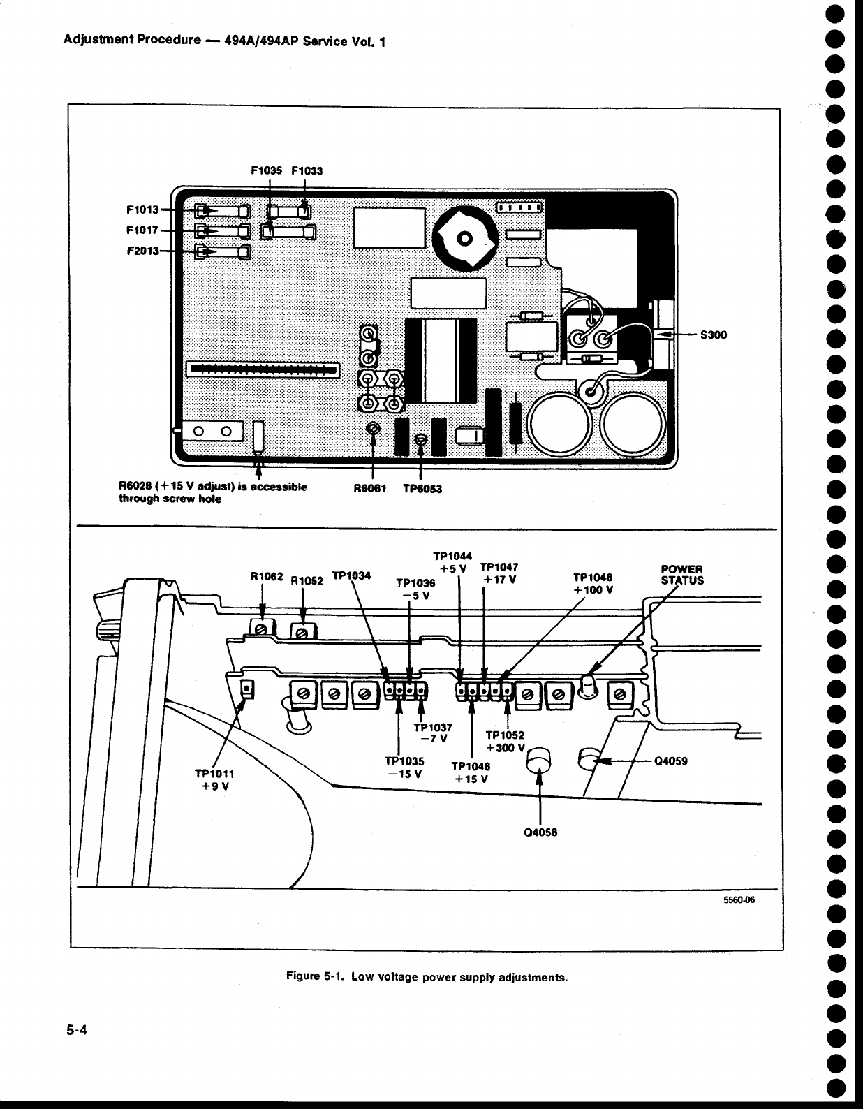
o
o
o
o
o
o
o
o
o
o
o
o
o
o
o
o
o
o
o
o
o
O
O
o
o
o
o
o
o
o
o
O
o
o
o
o
o
o
o
o
o
O
o
o
Adjustment Procedure
- 494A/494Ap
Service
Vol. 1
F1035
F1033
R6028
{+15 V adjurt} is acceccibte
throogfr
screw hole Rfl)6l TP6O53
€tr8
Figure 5-1- Low voltage power supply adiustments.
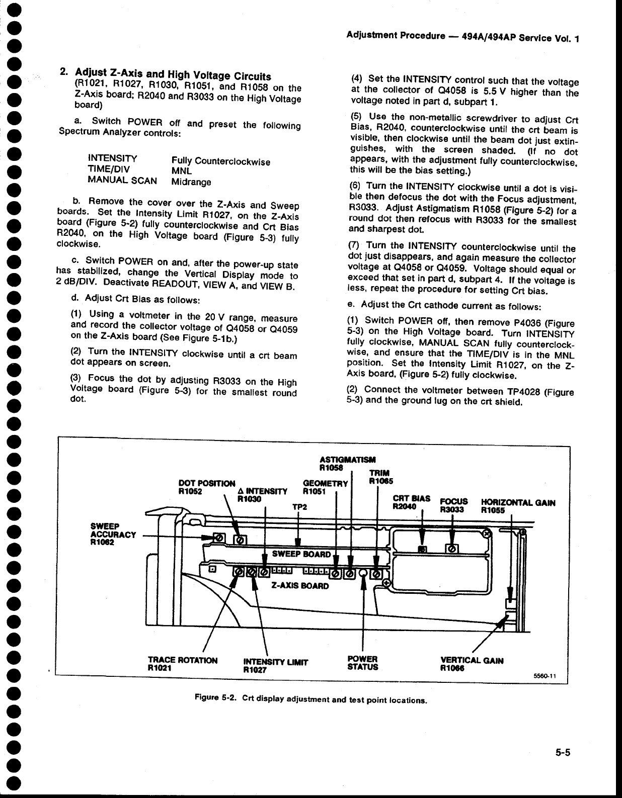
o
o
o
o
o
o
o
o
o
o
o
o
o
o
o
o
o
o
o
o
o
o
o
o
o
o
o
o
o
o
o
o
o
o
o
o
o
o
o
o
o
o
o
o
2. ^qlult Z-Axis
and
High
Votrage
Circuits
{110?1,
R1027,
Rlogo,-R1ost,
tno-ili0s8
on
the
Z-Axis
board; R2O4A
and R3030
on the High
Vottage
board)
a. Switch POWER
off and preset the foilowing
Spectrum
Anatyzer
controls:
Adjustment
Procedure
- 494A/494Ap
Service
Vot.
1
(4) Set
the INTENSITY
control
such
that
the voltage
at the coltector
of e4059 is 5.5 V higher
than the
voltage
noted
in
part
d, subpart
1.
(5) Use the non-metallic
screwdriver
to adjust
Crt
Bias,
R2040,
counterclockwise
until
the crt beam
is
visible,
then
clockwise
until
the
beam
dot
just extin-
guishes, with the scr€en shaded. (f no dot
1?pea.tj:
with
the adjustment
fuily
counterctockwise,
this will be
the bias
setting.)
(6) Turn
the tNTENStTy
ctockwise
until
a dot
is
visi_
ble
then
defocus
th€ dot
with
thE Focus
adjustment,
R3033.
Adjust
Astigmatism
R1OS8
(Figure
l5*lZl
tor
a
round dot then refocus
with R3033
for ttre smailest
and
sharpest
dot.
fl) Turn the tNTENStTy
counterclockwise
untit
the
dot
just disappears,
and
again
measure
the
collector
voltage
at Q4058
or e4059. Vottage
shoutd
equat
or
exceed
that
set
in
part
d, subpart
4. ll the voltage
is
less,
repeat
the
procedure
for setting
Crt
bias.
e. Adjust
the
Crt cathode
curent as
follows:
(1) Switch
POWER
off,
then remove
p4096
(Figure
5-3) on the High
Vottage
board. Turn |NTENSIW
fully clockwise,
MANUAL
SCAN fuily counterclock_
wise, and ensure
that the TIME/DIV
is in the MNL
position. S€t the Intensity
Limit R1022,
on the Z_
Axis
board,
(Figure
5-2) fuily
clockwise.
(2) Connect
the voltmeter
between
Tp402g
(Figure
5-3)
and
the
ground
lug
on
the crt
shietd.
INTENSITY
TIME/DIV
MANUAL
SCAN
Fully
Counterclockwise
MNL
Midrange
b. Remove
the cover
over the Z-Axis
and Sweep
boards. Set the Intensity
Limit R1027.
on fi," Z_Axis
Plr.l(Figure 5-2)
fuily
counterctockwise
anO
Crt Bias
12010,.
on rhe High Vo[age board figure 5_3)
fuily
clockwise.
c. Switch
POWER
on-and,
after
the
power-up
state
has stabilized,
chang_e
the Vertical
OiJpf"V
mode to
2 dBlDtv. DeactivatehEADOUT,
viEw l,'""0 vtEW
B.
d. Adjust
Crt Bias
as
follows:
(1) Using
a voltmeter
in the 20
V range,
measure
and
record
the collector
voltage
of a+06e
or e4059
on
the
Z-Axis
board (See
Figuie
5-1b.)
(2) Turn
the INTENSITy
clockwise
until
a crt beam
dot appears
on screen.
(3) Focus
the dot by adjusting
Rgogg
on the High
v€ttage
board (Figure
s_3)
toi tne smailest
round
dot.
5-5
ASTmAnSt
Rr058
GEOTETRY
A D{TEilSTY
Rrqm Rr051
SWEEP
ACCURACY
R1002
POUER
STATUS YERTICAL GAIN
RlOGO
Figure
5-2. Crt display adjustment
and test point locaiions.
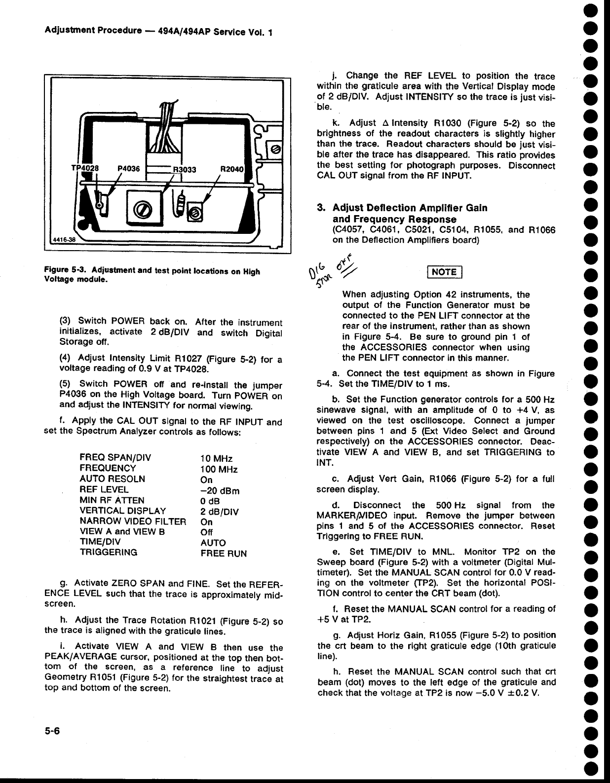
AdJustmant
Procedure
- 494A/4g4Ap
Service
Vot.
.l
Figure
5-3. Adiustment
and
test
point
locations
on Hlgh
Voltage
module.
(3) Switch POWER
back on. After
the instrument
initializes,
activate 2 dB/Dtv and switch Digital
Storage off.
(4) Adjust Intensity
Limit R1027 (Figure
5-2) for a
voltage
reading
of 0.9
V at
Tp402B.
(5) Switch POWER
off and re-instail
the jumper
P4036 on the High Vottage
board. Turn
pOWER
on
and
adjust
the
INTENSITy
for normalviewing.
f. Apply
the CAL OUT signat
to the RF tNpUT
and
set
the
Spectrum
Analyzer
controls
as
follows:
FREQ
SPAN/D|V 10
MHz
FREQUENCY 100
MHz
AUTO
RESOLN On
REF
LEVEL _2OdBm
MIN
RF
ATTEN O
dB
VERT|CAL
DTSPLAY 2 dBiDtv
NARROW
VTDEO
FTLTER On
VIEW
A and
V|EW B Off
TIME/DIV AUTO
TRIGGERING FREE
RUN
g. Activate
zERo
spAN and
FINE.
s€t
th€
REFER_
ENCE LEVEL
such
that
the trace is approximately
mid-
screen.
h. Adjust
the Trace Rotation
R1021 (Figure
S-2) so
the
trace is aligned
with
the
graticule
lines.
i. Activate VIEW A and VIEW B then us€ the
PEAK/AVERAGE
cursor,
positioned
at the
top then
bot-
tom of the screen, as a reference
line to adjust
Geometry
R1051
(Figure
S-2)
for the straightest
trace
at
top and
bottom of the screen.
j. Change
the REF LEVEL to position
the trace
within
the
graticule
area
with
the
Vertical
Display
mode
of 2 dB/DlV. Adjust
INTENSITY
so the trace is
just
visi-
ble.
k. Adiust A Intensity R1030 (Figure
5-2) so the
brightness of the readout characters is slightly
higher
than
the trace. Readout
characters should
be just visi-
ble
after
the trace
has
disappeared.
This
ratio
provides
the best setting
for photograph purposes.
Disconnect
CAL OUT
signal
from the
RF
INPUT.
3. Adiust
Deflection
Amplifier Gain
and
Frequency
Response
(C4057,
C4061, C5021,
C5104,
R1055,
and
R1066
on the Deflection
Amplifiers
board)
O
o
O
o
o
o
o
o
o
o
o
o
o
o
o
o
o
o
o
o
o
o
o
o
o
o
o
o
o
o
o
o
o
o
o
o
o
o
o
o
o
o
o
o
,r:**
When adjusting
Option 42 instruments,
the
output of th€ Function
Generator
must be
connected
to the PEN LIFT connector at the
rear
of the
instrument,
rather
than
as
shown
in Figure
5-4. Be sure
to ground pin 1 of
the ACCESSORIES
connector
when using
the
PEN
LIFT connector in
this
manner.
a. Connect the test equipment
as shown
in Figure
5-4. Set the
TIME/DIV
to 1 ms.
b. set the Function
generator
controls for a 500 Hz
sinewave signal,
with an amplitude of 0 to +4 V, as
viewed on the test oscilloscope.
Connect
a jumper
between
pins 'l and 5 (Ext
Video
Select
and Ground
respectively) on the AoCESSoRIES connector. Deac-
tivate
VIEW A and VIEW B. and set TRIGGERING
to
INT.
c. Adiust Vert Gain, R1066
(Figure
5-2) for a full
screen
display.
d. Disconnect the 500
Hz signal from the
MARKERIVIDEO input. Remove
the jumper between
pins 1 and 5 of the ACCESSORIES
connector.
Reset
Triggerlng
to FREE
RUN.
e. Set TIME/OIV to MNL. Monitor TP2 on the
Sweep board
(Figure
5-2)
with
a voltmeter
(Digital
Mul-
timeter). Set the
MANUAL
SCAN
controlfor 0.0 V read-
ing on the voltmeter
$P2). Set the horizontal POSI-
TION control
to center
the
CRT
beam
(dot).
f. Reset
the
MANUAL
SCAN
control for a reading
of
+5 V at
TP2.
g. Adjust Horiz
Gain,
R1055
(Figure
5-2) to position
the crt beam to the right
graticule
edge
(10th
graticule
line).
h. Reset the MANUAL SCAN
control
such
that crt
beam
(dot)
moves
to the left edge of the graticule
and
check
that the
voltage atTP2 is
now
-5.0 V *0.2 V.
5-6
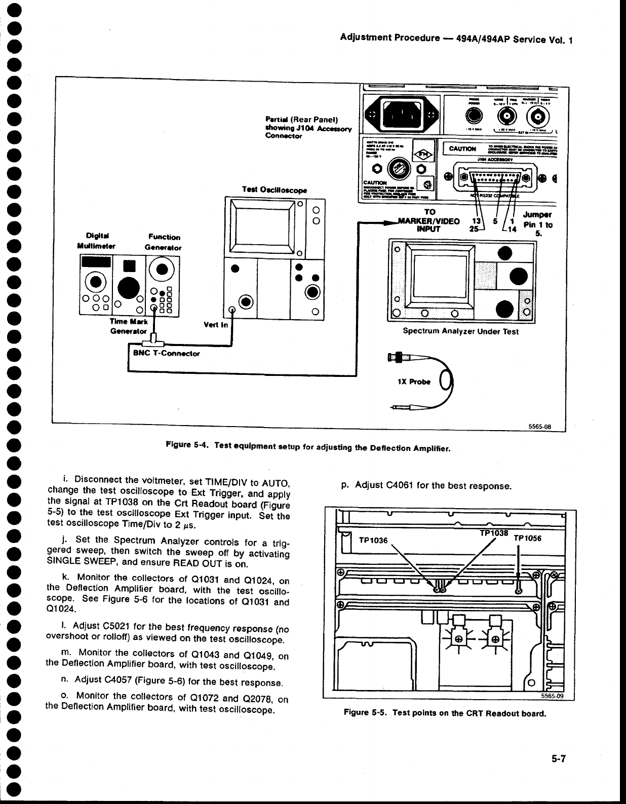
o
o
o
o
o
o
o
o
o
o
o
o
o
o
o
o
o
o
o
o
o
o
o
o
o
o
o
o
o
o
o
o
o
o
O
o
o
o
o
o
o
o
o
o
Figure 5-4. Test equlpment setup for adiusting the D€flection Amplifier.
Adiustment
Procedure
- 4g4Al4g4Ap
Service
Vol.
1
p. Adjust
C4061 for
the best
response.
Figure 5-5. Test points on the CRT Readout board.
i. Disconnect
the
voltmeter,
set
TIME/DIV
to AUTO,
change
the test oscilloscope
^to
Ext Trigger,
and
apply
the signat
at Tp10g8
on the Crt neadojt-board
fiiuri
5-5)
to the
test oscilloscope
Ext Trigger
input. Set
the
test oscilloscope
TimeiDiv
to 2 ;rs.
j. set the spectrum
-
Analyzer
controls
for a trig-
gered
sweep,
then switch
the sweep
off by aetivating
SINGLE
SWEEP,
and
ensure
netO OUT is
on.
k. Monitor
th€ collectors
of e1O31
and e1
024,
on
the Deflection
Amplifier
board, with the test oscillo-
See Figure
5-6 for the locations
of e1031
and
01024.
l. Adjust
C5021 tor
the
bestfrequencyresponse(no
overshoot
or rolloff)
as
viewed
on
the
tesiosciiloscope,
m. Monitor
the collectors
of e1043
and
e1049,
on
the Deflection
Amplifier
board,
with
test oscilloscope.
n. Adjust
C4OS7
(Figure
5_6) for
the
best
response.
o. Monitor
the collectors
of e1072 and e207g,
on
the
Deftection
Amplifier
board,
with
test o."illo."op".
P.rtad (Rear Panel)
drowing Jl(X Acccrorv
Connrcror a@
@JgESI
(
51
1{
Jumpcr
Pin I to
5.
BllC T-Conneclor
T.d O|Glnoacopc
o
ooo
Oo
Spectrum Analyzer
Under Test
5-7
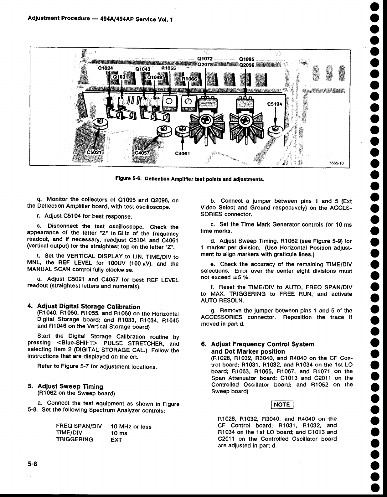
Adfustment
Procedure
- 4g4Ll4g4Ap
Servtce
Vot. 1
Flgure
5€. Deflection
Amptilier
test points and adiuetments.
o
o
o
o
o
o
o
o
o
o
o
o
o
o
o
o
o
o
o
o
o
o
o
o
o
o
o
o
o
o
o
o
O
o
o
o
o
o
o
o
o
o
o
o
q. Monitor
the collectors
of e1095 and e20g6, on
the Deflection
Amplifier
board,
with
test oscilloscope.
r. Adjust
C5104
tor best
response.
s, Disconnect
the test oscilloscope. Check
the
appearance
of the letter *Z'"
in GHz of the frequency
readout,
and if necessaryt
readjust
CS1O4
and C406i
(vertical
output)
for the straightest
top
on
the
letter
"Z-.
t. set the vERTtcAL
DtspLAy to LtN,
T|ME/D|V
to
MNL, the REF LEVEL
for 100UV
(100pV),
and the
MANUAL
SCAN control
fully
clockwise.
u. Adjust C5021
and C4057
for best REF
LEVEL
readout (straightest
leters and
numerals).
4. Adjust Digital Storage Calibration
(R1040,
Rl050,
R1055,
and
R1060
on
the Horizontal
Digital Storage board;
and R1033,
R1Og4,
R1045
and
R1046 on
the Vertical
Storage
board)
Start the Digital Storage Calibration
routine by
pressing <Blue-SHIFT> PULSE STRETCHER,
and
selecting
item 2 (DIGITAL
STORAGE
CAL.) Foilow
the
instructions
that ar€
displayed
on
the crt.
Refer
to Figure
5-7 for
adjustment
locations.
5. Adiust Sweep Timing
(Rl062
on
the
Sweep
board)
a. Connect
the test equipment
as shown
in Figure
5-8. Set the
following
Spectrum
Analyzer
controls:
FREQ
SPAN/D|V 10 MHz
or
tess
TIME/D|V 10 ms
TRIGGERING EXT
5-8
b. Connect
a jumper between
pins 1 and 5 (Ext
Video
Select and Ground respectivety)
on the ACCES-
SORIES
connector.
c. Set
the
Tim€
Mark Generator controls
for 10 ms
timE marks.
d. Adjust
Sweep Timing, Rl062 (see
Figure
5-9)
for
1 marker
per division.
(Use
Horizontal Position
adjust-
ment
to align markers
with
graticule
lines.)
e. Check
the accuracy
of the remaining
TIME/DIV
selections. Error
over the center
eight
divisions
must
not exceed !.5 o/o.
f. R€set
the TIME/D!v
to AUTo, FREQ
SPAN/D|V
tO MAX,
TRIGGERING
tO FREE RUN, ANd
ACtiVAtE
AUTO
RESOLN.
g. Remove
the
jumper
between
pins
1 and 5 of the
ACCESSORIES
connector. Reposition
the trace if
moved in
part
d.
6. Adjust Frequency Control System
and Dot Marker position
(R1028,
R1032, R3040, and R4040 on
the CF Con-
trol
board; R1031, R1032,
and R1034 on
the
1st LO
board;
R1063, R1065, R1067,
and R1071
on the
Span
Attenuator
board;
C1013
and C2011
on the
Controlled Oscillator board: and R1052 on the
Sweep board)
R1028, R1032, R3040, and R4040 on the
CF Control board: Rl031, R1032, and
R1034
on the 1st LO board:
and
C'!013
and
C2011 on the Controlled Oscillator board
are adjusted
in part d.
{di
' ##
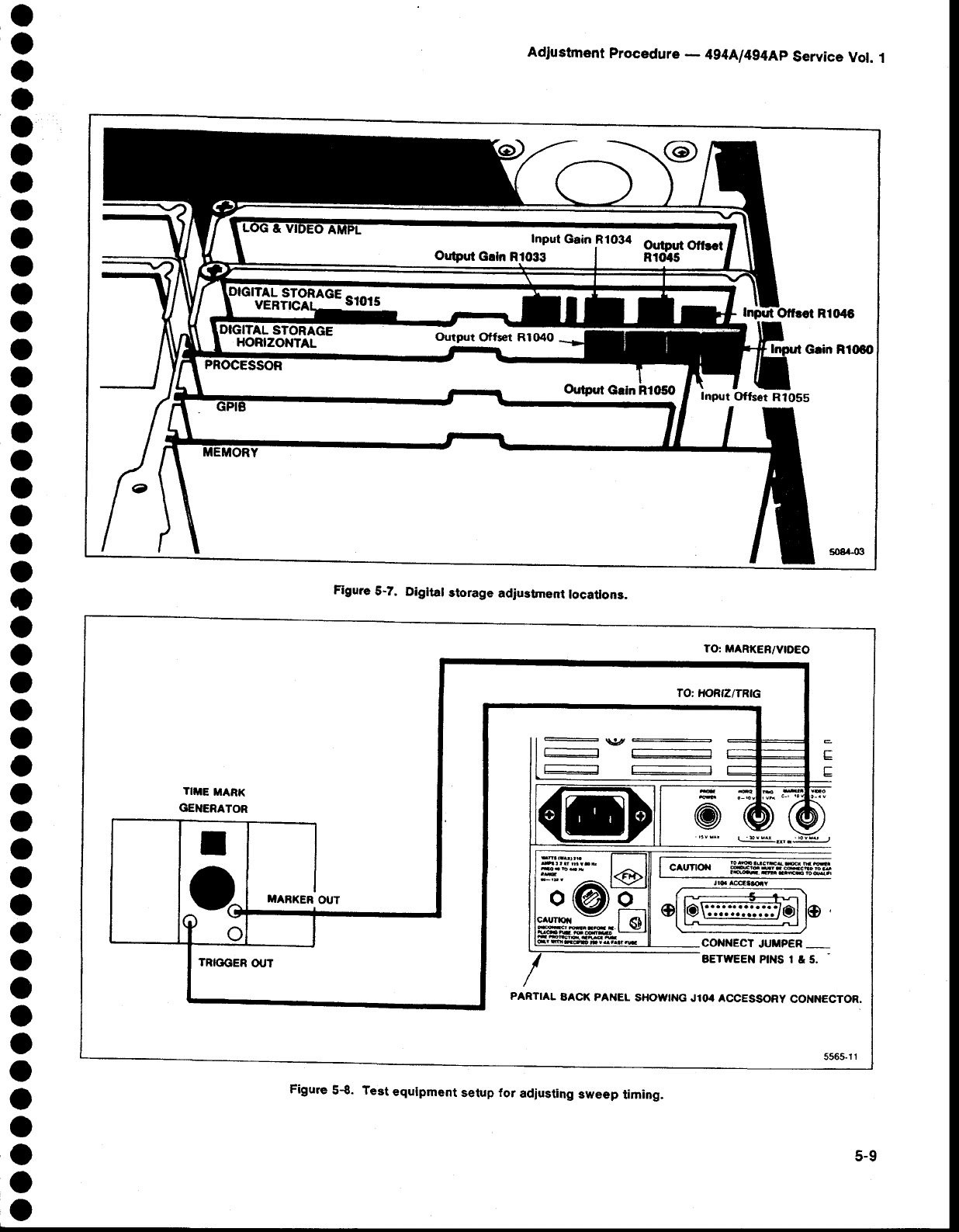
o
o
o
o
o
o
o
o
o
o
o
o
o
o
o
O
o
o
o
o
o
o
o
o
o
o
o
o
o
o
o
o
o
o
o
o
o
o
o
o
o
o
o
o
AdJustment
Procedure
- 494A1494Ap
Service
Vot.
1
lnput Gain,RlO3a O.rtput Of*t
ouFur
Garn
R1033 | nrors
iITAL STORAGE
HORIZONTAL
RIINC
G.io R1OOo
Figure 5-7. Digltal storage adiustment locations.
TO: TTARKEBiVID8O
TITE TIARK
GEI{ERATOR ffi
Itull
\=z
BETWEEI{PINSl&5.
PARTIAL BACK PANEL SHOWING
Jl(X ACCESSORY
COilNECTOR.
Figure 5{. Test equlpment setup lor adiusting
sweep timing.
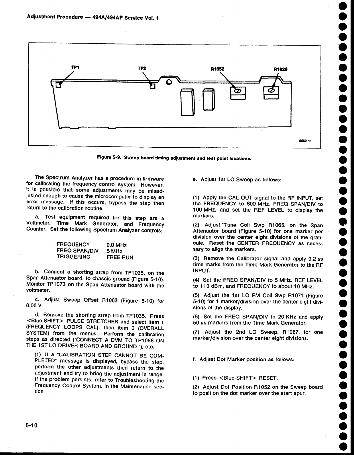
Adjustnent Procedure
- 4g4A/4g4Ap
Servtce
Vot.
1
Figure 5-9. Sweep board tlming adiustment and test point locations.
o
o
o
a
o
O
o
o
o
o
o
o
o
o
o
o
o
o
o
o
o
o
o
o
o
o
o
o
o
o
o
o
o
o
o
o
o
o
o
o
o
o
o
o
The
Spectrum
Analyzer
has
a procedure
in firmware
for calibrating
the frequency
control
system. However,
it is possible
that some adjustments
may be misad_
justed
enough
to cause
the microcomputer
io display an
€rror message. lf this occurs,
bypass
the step then
return
to the
calibratlon
routine.
Test equipment
required
for this step are a
Voltmeter, Time Mark Generator, and Fiequency
Counter.
Set
the
following
Spectrum
Analyzer
controls:
FREQUENCY 0.0 MHz
FREQ
SPAN/D|V 5 MHz
TRIGGERING FREE
RUN
b. Connect
a shorting
strap from Tplogs. on the
Span Attenuator
board,
to chassis ground
(Figure
5-10).
Monitor
TP1073
on the Span
Attenuator
board
with
the
voltmeter.
- --c: Adjust Sweep Offset R1063 (Figure
S-10) for
0.00
v.
d. Remove
the shorting
strap
from
Tp1035. press
<BIUe.SHIFT>
PULSE
STRETGHER
and
select
item
1
(FREOUENCY
LOOPS CAL), then item 0 (OVERALL
SYSTEM)
from the menus. perform the calibration
steps
as directed
('CONNECT
A DVM
TO Tp105g
ON
THE 1ST
LO DRTVER
BOARD
AND
GROUND,),
etc.
(1) lf a "CAL|BRATION
STEP
CANNOT
BE COM-
PLETED"
message
is displayed,
bypass
the step,
perform
the other adjustments
then return
to the
adjustment
and
try to bring
the
adjustment
in range.
lf the
problem
persists,
refer
to Troubleshooting
the
Frequency
Control
System,
in the
Maintenance
sec_
tion.
e. Adjust
1st
LO
Sweep
as
follows:
(1) Apply the
CAL
OUT signal to the RF tNpUT,
set
the FREQUENCY
to 600 MHz, FREQ
SPAN/DIV
to
100 MHz, and set the REF LEVEL
to display
the
mark€rs,
(2) Adjust'Tune
Coil Swp R1065, on the Span
Attenuator
board (Figure
5-10)
for one marker
per
division
over
the center eight
divisions of the
grati-
cule. Reset
the CENTER FREQUENCY
as neces-
sary
to align
the markers.
(3) Remove
the Calibrator signal
and apply
0.2
ps
time
marks from
the Time
Mark
Generator to th€ RF
INPUT.
(4) Set
the FREQ
SpAN/Dtv
to 5 MHz,
REF
LEVEL
to +10
dBm,
and
FREQUENCY
to about
10 MHz.
(5) Adjust
the lst LO FM Coil
Swp R1071 (Figure
5-10) for 1 marker/division
over the center eight
divi-
sions of
the
display.
(6) Set th€ FREQ
SPAN/DIV to 20 KHz and appty
50
ps
markers from
the Time
Mark Generator.
n Adjust the 2nd LO Sweep, R1067,
for one
marker/division
over
the center
eight
divisions.
f. Adjust Dot Marker
position
as follows:
(1) Press
<Blue-SHIFT>
RESET.
(2) Adjust
Dot Position R1052 on
the Sweep
board
to position
the
dot marker over the start spur.
5-1
0
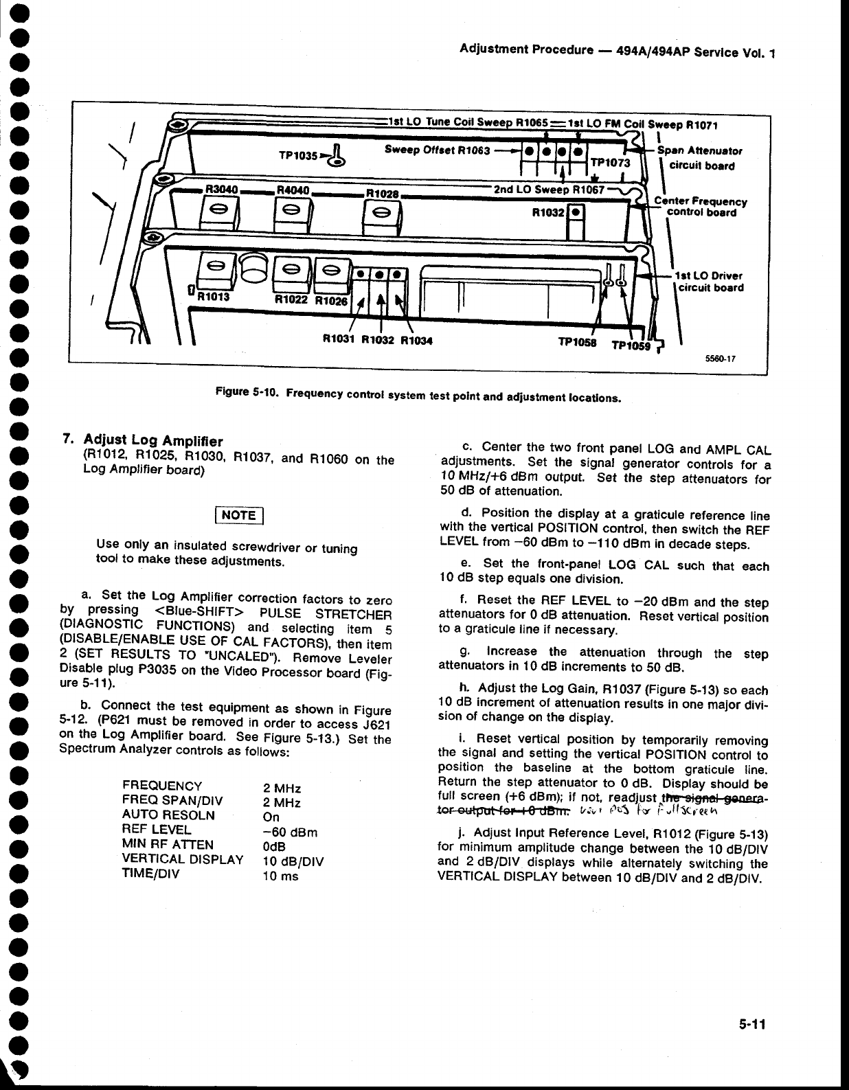
a
o
o
o
a
o
o
o
o
O
a
o
o
a
o
o
O
o
o
o
o
o
o
o
o
o
o
o
o
o
o
o
o
o
O
o
o
o
o
o
a
o
o
''
7. Adjust
Log Amptitier
(R1012,
R102S,
R1030,
R1037,
and
R.t060
on
the
Log
Amptifier
board)
Use
only
an insulated
screwdriver
or tuning
tool
to make
these
adjustments.
. a. Set
the Log Amplifier
correction
factors
to zero
b_y pressing (Bfue-SHtFT> PULSE STRETCHER
(DIAGNOSTIC
FUNCTTONS;
and setecting
item 5
(DISABLE/ENABLE
USE
OF
CAL
FACTORS),
tnen
item
2 (SET RESULTS
TO "UNCALED). Remove
Leveler
Disable
plug
P3035
on the
Video
processor
board
(Fig_
ure 5-1 1).
b. Connect
the t€st equipment
as shown
in Figure
5-12. (P621
must be removed
in order
to access
J621
on the Log Amplifier
board. See
Figure
S_1g.)
Set
the
Spectrum
Analyzer
controls
as
follovis:
FREQUENCY 2MHz
FREO
SPAN/D|V 2MHz
AUTO
RESOLN On
REF
LEVEL -60 ctam
MIN
RF
AfiEN OdB
VERT|CAL
DTSPLAY 1O
dB/DtV
TtMEiDtV 10
ms
c. Center
the two front
panel
LOG
and
AMPL
CAL
adjustments.
Set the signat
generator
controls
for a
10MHzl+6
dBm output. Set the step attenuators
for
50 dB
of attenuation.
d. Position
the
display
at a graticule
reference
line
with
the vertical
POSITION
control,
then switch
the
REF
LEVEL
from
-60 dBm
to -110 dBm
in
decade
steps.
e. S€t the front-panel
LOG CAL such that each
10
dB
step
equals
one
division.
f. Reset
the REF
LEVEL
to -20 dBm and
tha step
attenuators
for 0 dB attenuation.
Reset vertical position
to a
graticule
line if necessary.
g. Increase the attenuation
through the step
attenuators
in 10
dB increments
to 50 dB.
_ h- Adjust
the Log
Gain,
R1037
(Figure
S-13)
so each
10
dB increment
of attenuation
results
in one
major
divi-
sion
of change
on
thE
display.
. i. Reset
vertical
position
by temporarily
removing
the signal
and setting
the verticat
POSITION
control
to
position the baseline
at the bottom graticule
line.
Return
the step attenuator
to 0 dB. Display
should
be
full screen (+6 dBm);
if not, readjustJtrg*iglfial-gene@-
@ lzJ,r
rli,1 [v i:"lllCrerh
j. Adjust
Input
Reference
Level, R1012
(Figure
5-13)
for minimum
amplitude
change
between the
10
dB/DlV
and 2 dB/DlV displays
while alternately
switching
the
VERTICAL
DISPLAY
between
10
dB/DtV and
2 dB/DlV.
Adjustment
Procedure
- 494Ll4g4Ap
Servlce
Vol.
1
rPlo3s-.8
Tune
Coil R1065:ttl
R1031
Rro32 R10:t4
FM Coil
Swcco RtOZl
=?l I
Ccnter Frcqucncy
Span Attcnualor
\circgir
boild
control
boord
I
I
Ilst LO Orivct
lcircuit board
I
I556G17
Figure
5'10. Frequency
contror
system
test
potnt
and
adiustment
rocations.
5-11
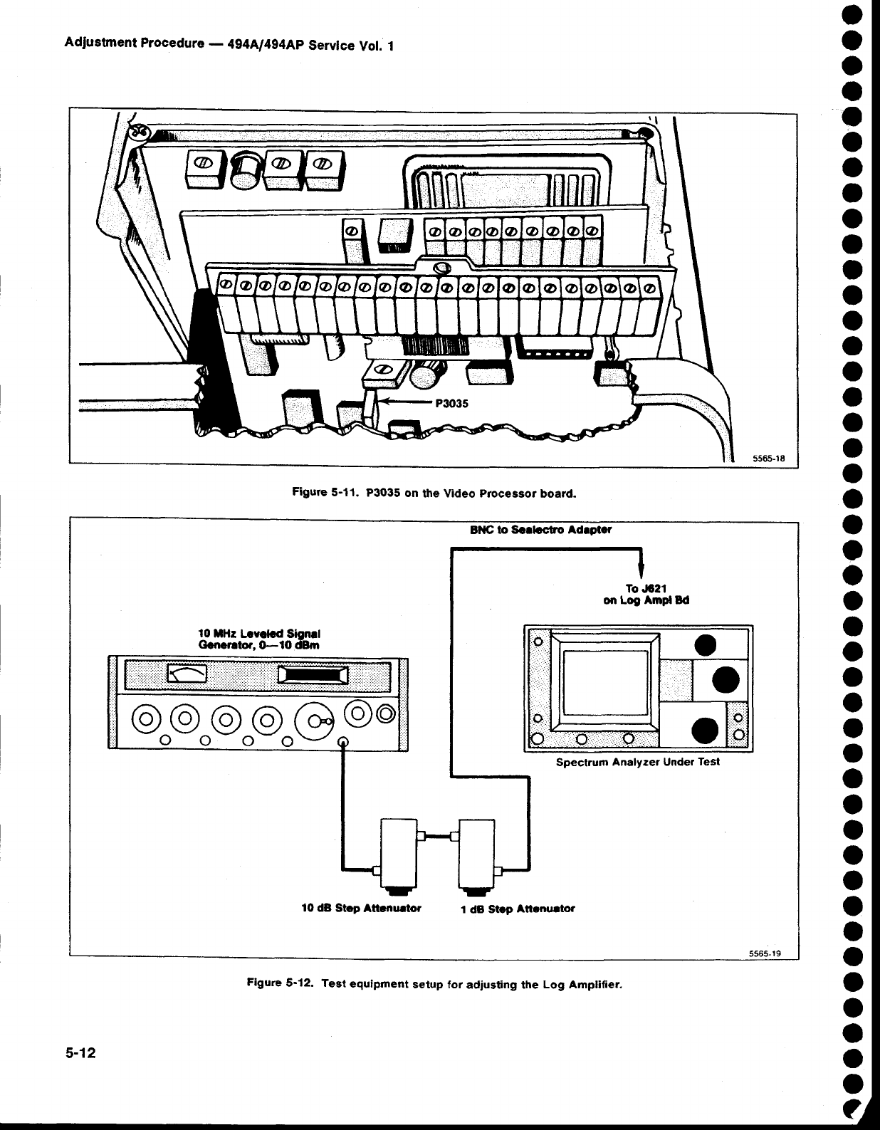
o
o
o
I
a
o
o
o
o
o
a
o
o
o
o
o
o
o
o
o
o
o
o
o
O
o
a
o
o
o
o
o
o
o
o
o
O
o
o
o
a
o
o
(?,
5565-19
Analyzer Under
Tesl
&21
Ampl
Bd
BilC fo Sorlos:tro Ad.gtCr
'lO dB Stcp Attcnu.tor 1 dB Stcp An nu.to.
m LHr Lcvclod Signrl
Gcocr.to?,0-lO dBm
To
on Log
Spectrum
@"o.@"@"G)Pt
I
I1
Figure 5-12. Test equlpment setup for adjusting the Log Amplifier.
Adrustment
Procedure
- 4g4Ll4g4Ap
Servtce
Vot. 1
Figure 5-'11. P3035 on the Video processor board.
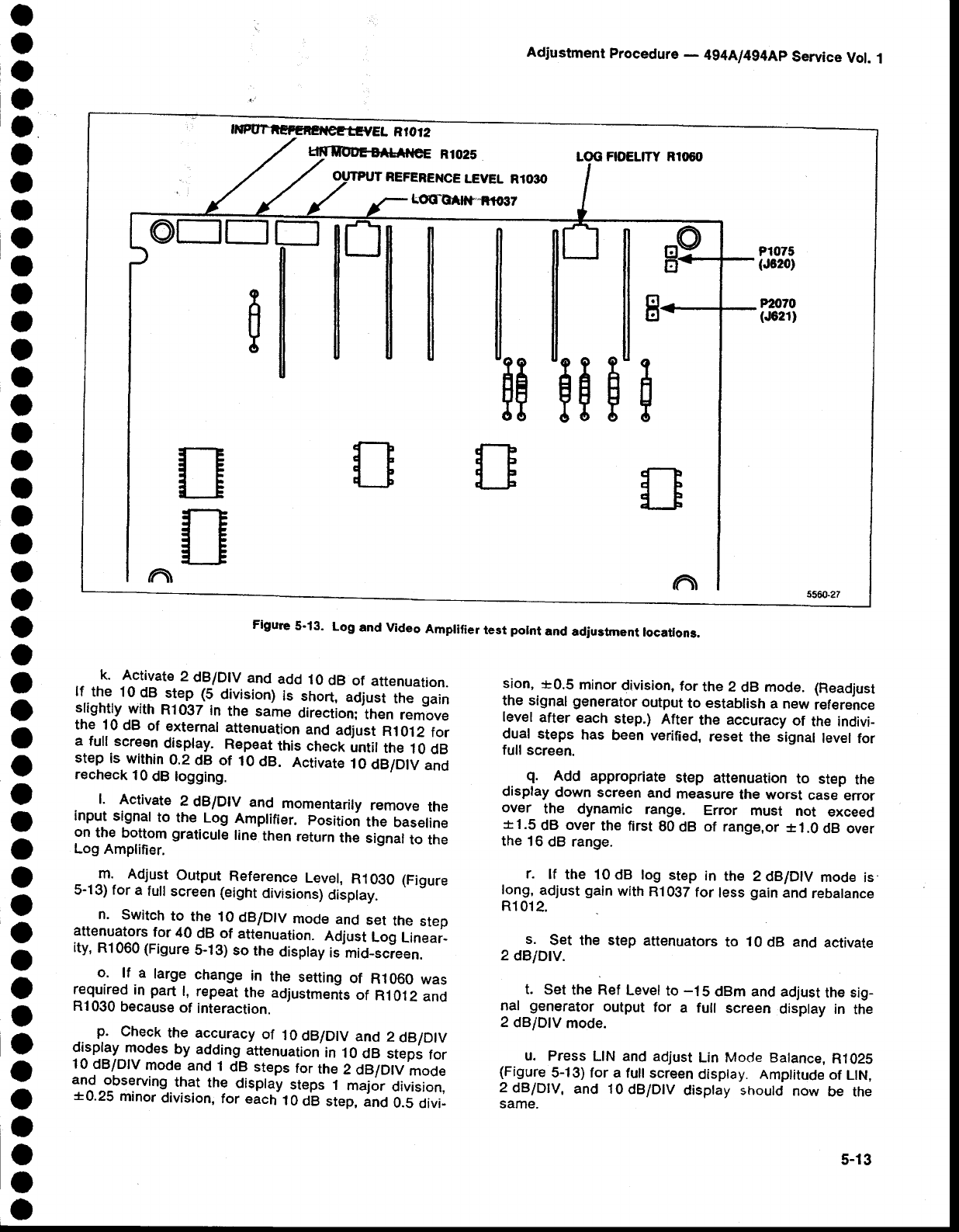
o
o
O
o
I
I
o
I
o
o
o
t
o
o
o
o
o
I
o
o
o
o
o
o
o
o
o
o
a
o
o
o
o
o
o
o
a
o
o
o
a
o
o
O
.- .k. lctlvate 2 dB/Dtv and
add
10
dB of artenuation.
lf..the
1098 step (S
division)
is short,
adjust
the gain
slightly
with
R'|037
in the same
direction;'then
rem-ove
the 10
dB of external
attenuation
and
adjust
R1012
for
a full.screen
display.
Repeat
this
check
untit
the
10
dB
step
is
within
0.2
dB
of 1O
dB. Activate
10
dB/OtV
and
recheck
10
dB logging.
. l: Activate
2 dB/Dlv and momentarily
remove
the
input
signal
to the Log Amplifier.
position
the baseline
on
the bottom graticule
line
then
return
the
signal
to the
Log
Amplifier.
_ 11 Adjust
Output-
Reference
Level,
R1030 (Figure
5-13) for
a
full
screen
(eight
divisions)
display.
n. Switch
to the l0 dB/DtV
mode
and set the step
attenuators
for
40 dB
of attenuation.
Adjust
Log
Lineai_
ity,
R1060 (Figure
5-10)
so
the
disptay
is mid_screen.
o lf a large
change
in the setting
of R1060
was
f-q-Treg
in part
t, repeat
the adjustmenls
of R1012
and
R1
030
because
of interaction.
p. Check
the accuracy
of 10
ctB/DtV
and 2 dB/DtV
gfqPy-T9des by adding
attenuation
in 10
dB steps
for
10
dB/DlV
mode
and
1
dB steps
for
the
2
dBlDtV'rnode
an! -gbsqrving
that the disptay
steps
1 major
division,
*0.25 minor
division,
for
eictrl0 A'e
step,
jnd 0.5
divi_
sion,
r0.5 minor
division,
for
the 2 dB mode. (Readjust
the
signal
generator
output
to establish
a new
reference
level
after
each
step.) After
the accuracy
of the indivi_
dual steps has been
verified,
reset the signal
level
for
full
screen.
q. Add appropriate
step attenuation
to step the
display
down screen
and
measure
the worst
case
error
over the dynamic range. Error must not exceed
11.5
dB over
the
first
80
dB of range,or
11.0
dB over
the
16
dB range.
r. lf the 10
dB log step
in the 2
dB/DtV
mode
is
long,
adjust
gain
with
R1 097
for
less
gain
and
rebalance
R1
01
2.
s. Set the step attenuators
to 10
dB and activate
2 dBlDtv.
t. set the Ref
Levet
to
-15 dBm and
adjust
the sig-
nal generator
output
for a full screen
display in the
2
dB/DlV
mode.
u. Press
LIN and
adjust
Lin MocJe Balance,
R102S
(Figure
5-13) for a
full screen
disptay. Amplitude
of
LtN,
zdBlDlV,
and 10dB/DtV
disptay
should
now
be the
sarne.
Adjustment
Procedure
- 4g4A/4g4Ap
Service
Vol.
1
Pl075
(J620)
Pm70
(J621)
ffwu"nffEneilercYEl R10f2
LOG
FIOELTTY R1O6O
REFERENCE
LEVEL RIOIIO
Lqrc^$t*FroilT
L-
il
n
@ftftfl ll
fill
oll HHF
l--E
L-.,E
il
Figure
5'13. Log and video Ampri{ier
test pornt
and
adiustment
rocations.
5-13

Adjustment
Procedure
- 494[l4g4Ap Service Vot.
1
Figurc
5-14. Test equipment
3etup
tor adiusting tlre Varlable Re3olution
rnoOut".
5[ton'"*' ffi
I Filrc.
sotocr I
6097-18
,
o
o
a
o
o
o
a
o
o
a
o
o
o
o
o
o
o
o
o
o
o
o
o
o
o
o
o
I
O
o
o
o
o
O
o
a
o
O
o
o
o
o
a
v. Check LIN disptay linearity by adding 6 dB,
12
dB. and 18
dB of attenuation
and note
the display
step down from full screen
to, 4 +0.4, 6 *0.4, and
7
*0.4 divisions.
w. Remove the signal generator from the Log
Amplifier input
jack and reptace
p621. Reptace
p3035
on the Video
Processor
board.
8. Adjust Resolution
Bandwidth
and
Shape
Factor
(c304r, c5048, C505s, R106s, R3015,
R3029,
R3033, and R4025
on the VR 2nd Filter
Setect
board)
(c1034, C1044, C1046, C2030, C3O3O, C3039,
C3045, and R1027
on the VR 1st Fitter
Setect board)
(c1032, C4015, G4028, C4036, C4045, C4051,
C4060, R3010, and R3025 in the 10
Hz Fitter
Assembly)
(R2025
on the 10 dB Gain Steps board)
The 3 dB down bandwidth of each filter section
should be as wide or slighfly wider than the 6 dB down
point of the combined two filter sections.
The filters in each section are aligned
separately,
then
a signal is applied
through
both the first and second sections. The
final adjustments trim filter shape and
bandwidth. Because of interaction,
it is
easy
to offset
one filter to compensate for
another misadjusted
filter; therefore,
only
adjust each
filter
in small increments.
Before calibrating the Variable Resolution
Bandwidth
and Gain, disable use of cal factors by
pressing <Blue-SHIFT> PULSE STRETCHER
and
selecting
item
5, then
item 0.
a. Equipment setup is shown
in Figure
5-14.
(1) Remove and install the Variable Resolution
module
on an extender.
(2) Use a Sealectro male-to-male
adapter
ancl
coax-
ial cable
to connect the 10 MHz lF output signal,
from the 3rd Converter, to the input of the second
s€ction
(make
connection
from plug removed
from
J693
to J683).
5-14
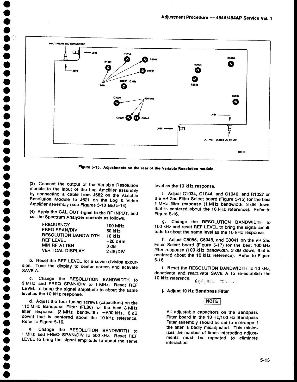
o
o
o
o
o
o
t
t
o
I
o
O
o
O
o
o
o
a
o
o
o
o
o
a
a
o
O
o
o
a
o
O
o
O
o
o
O
o
a
o
o
o
o
o
Flgure
5'15. Adiu3tmonts
on the rear
of tre Variabre
Resorudon
modure.
(3) Connect
the output of the Variable
Resolution
module
to the input.
of lhe Log Amplifier
assembly
by connecting
a cable from J6g2
on the Variable
Resolution
Module to J621 on th€ Log & Video
Amplifier
assembly
{see
Figures
S-10 and
-S-t+;.
(a) Apply
the
CAL
OUT signat
to th€ RF
tNpUT,
and
set
the
Spectrum
Analyzer
controls
as
follows:
FREQUENCY 100
MHz
FREO
SPAN/D|V S0 kHz
RESOLUTTON
BANDWTDTH
10
kHz
REF LEVEL -20dBm
MtN
RF
ATTEN 0 ctB
VERTICAL
DTSPLAY 2 dBl}tv
b. Reset
the
REF
LEVEL
for a seven
division
excur_
sion Tune
the display
to center
screen
and activate
SAVE
A.
- c. Change the RESOLUTTON
BANDWIDTH
to
3 MHz and FREQ
SPAN/D|V
to 1
MHz. Reset
REF
LEVEL
to bring
the signal
amplitude
to about
the
same
level
as
th€ 10 kHz
response.
-d. Adjust
the four tuning
screws
(capacitors)
on
the
110
MHz Bandpass
Fitter (FL361
foi tire best 3 MHz
fi-lter
.
response (3
MHz bandwidth *600 kHz, 6 dB
down) that is centered about the 10
kHz reference.
Refer
to Figure
5-1
6.
e. Change the RESOLUTTON
BANDWIDTH
ro
1 MHz and FREQ
SPAN/D|V
to 500
kHz. Reset REF
LEVEL
to bring
the signal
amplitude
to about
the same
level
as
th€
10 kHz response.
f. Adjust
C1034,
C1044,
and
C1046,
and
R1027
on
the VR
2nd Filter
Select
board (Figure
5,15) for the
best
1 MHz filter response
(1
MHz bandwidth,
3 dB down.
that is centered
about
the 10
kHz reference).
Refer
to
Figure
5-16.
g. Change the RESOLUTTON
BANDWTDTH
ro
100
kHz
and
reset
REF LEVEL
to bring
the
signat
ampti-
tude
to about
the same
level
as
the
l0 kHz
response.
h. Adjust
C5055,
C5048, and
C3041
on the VR
2nd
Filter
Select
board (Figure
5-17)
for the best .lOO
kHz
filter
response
(100
kHz bandwidth,
3 dB down,
that
is
centered
about
the 10 kHz reference).
Refer
to Figure
5-1
6.
i. RESET
th€ RESOLUTION
BANDWIDTH
tO 1O KHZ,
deactivate
and reactivate
SAVE A to re-establish
the
10
kHz
reference.
n
r( ', -' -5 -
J. Adlust
10 Hz
All adjustable
capacitors
on the Bandpass
Fifter
board
in the 10
Hzfi00 Hz Bandpass
Filter
assembly
should
be
set
to midrange
if
the
filter is badly misadjusted.
This minim-
izes
the number of times
interacting
adjust-
rnents must be repeated to eliminate
interaction.
Bandpass
Fllter
lNorE-l
AdJustment
Procedure
- 4g4[l4g4Ap Service
Vot.
1
5-15
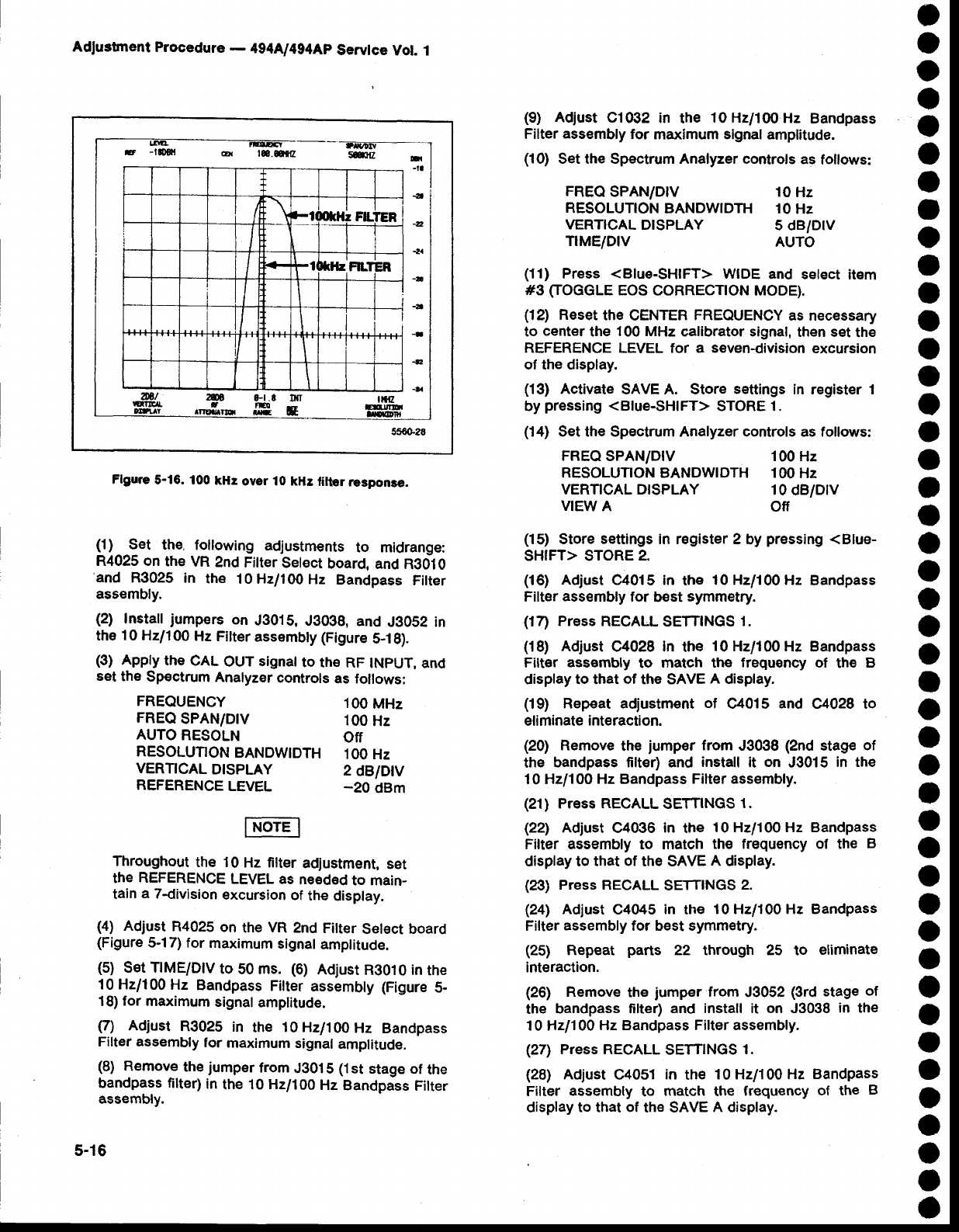
Adlustnent Procedure
- 494ful4g4Ap
Servtce
Vot. 1
Flgure
5-16. 100
kHz
over l0 kHz
litter
respona€.
(1) Set the, foltowing
adjustments
to midrange:
R4025 on
the
VR
2nd
Fitter
Select
board,
and
R3OIO
'and R3025
in the 10Hz/100H2
Bandpass
Fitter
assembly.
(2) Install
jumpers
on J30i5, JgogS, and J3052 in
the
10
Hzll00 Hz Fitter
assembty
(Figure
5-ig).
(3) Apply
the
CAL
OUT
signat
to th€
RF
tNpUT, and
set
the
Spectrum
Analyzer
controls
as follows:
FREQUENCY 100
MHz
FREQ
SPAN/D|V 100
Hz
AUTO
RESOLN Off
RESOLUTTON
BANDWTDTH 100
Hz
VERT|CAL
DTSPLAY 2 dB/DtV
REFERENCE
LEVEL -20 dBm
Throughout
the 10
Hz
ftlter
adiustment,
set
the
REFERENCE
LEVEL
as
needed
to main-
tain
a 7-division
excursion
of the
display.
(4) Adjust
R4025
on the
VR
2nd
Filter
Set€ct board
(Figure
5-17)
for maximum
signal
amplitude.
(5) Set TIME/D|V
to 50 ms. (6) Adjust
Rg0i0 in
the
10
Hzl100 Hz Bandpass
Fitter
assembty (Figure
5-
18)
for maximum
signal
amplitude.
0 Adjust
R3025
in the 10Hz/100H2
Bandpass
Filter assembly
for maximum
signal
amplitude.
(8) Remove
the
jumper
from
JO01S
(1st
stage
of the
bandpass filter)
in the 10 Hzl100
Hz
Bandpass
Filter
assembly.
s-l6
(9) Adjust
C1032
in the loHz/lfi)Hz Bandpass
Filter
assembly
for maximum slgnal amplitude.
(10) Set the Spectrum Analyzer controls
as follows:
FREQ
SPAN/DIV '10
Hz
RESOLUTION
BANDWIDTH 10
Hz
VERTTCAL
DTSPLAY 5 dB/DlV
T|ME/D|V AUTO
(11) Press (Blue-SHIFT> WIDE
and select
item
#3 CTOGGLE
EOS
CORRECTTON MODE).
(12) Reset
the
CENTER
FREQUENCY
as necessary
to center
the 100 MHz
calibrator signal,
then set
the
REFERENCE
LEVEL for a seven-division
excursion
of the display.
(13) Activate
SAVE A. Store s€ttings
in register 1
by
pressing
<Blue-SHIFT>
STORE
1.
(14) Set the Spectrum Analyzer controls as follows:
FREQ
SPAN/DIV 100
Hz
RESOLUTION
BANDWIDTH 100
Hz
VERTICAL DTSPLAY 10
dB/DlV
VIEW
A Otr
(15) Store settings in register 2 by
pressing
<Blue-
SHIFT> STORE
2.
(16) Adjust C4015 in the 10Hz/100H2
Bandpass
Filter
assembly
for b€st
symmetry.
(17) Press RECALL
SETTINGS
1.
(18) Adjust
C4028 In the 10Hz/100H2
Bandpass
Filtsr assembly to match th€ trequency of th€ B
display to that of the sAVE A display.
(19) Repeat adiustment of C4015 and C4028 to
eliminate
interaction.
(20) Remove
the jumper from J3038 (2nd stage of
the bandpass filter) and install
it on J3015
in the
10 Hzl100
Hz Bandpass Filter assembly.
(21) Press RECALL
SETTINGS
1.
(22) Adjust
C4036
in the 10Hz/10OHz Bandpass
Filter assembly to matoh th€ frequency of the B
display to that of the sAvE A display.
(23) Press RECALL
SETTINGS
2.
(24) Adjust C4045
in the 10 Hzl100 Hz Bandpass
Filter
assembly
for best symmetry.
(25) Repeat parts 22 through 25 to eliminate
interaction.
(26) Remove
the jumper from J3052 (3rd stage of
the bandpass filter) and install it on J3038
in the
10 Hzll00
Hz Bandpass Filter assembly.
(27) Press RECALL
SETTINGS
1.
(28) Adjust
C4051
in the 10Hz/100H2
Bandpass
Filter assembly to match the frequ€ncy
of the B
display to that
of th€ SAVE
A display.
o
o
o
o
a
o
o
a
o
o
a
a
o
o
o
o
o
o
o
o
o
o
o
o
o
o
O
o
o
o
o
o
I
o
o
o
o
o
o
o
o
o
o
a
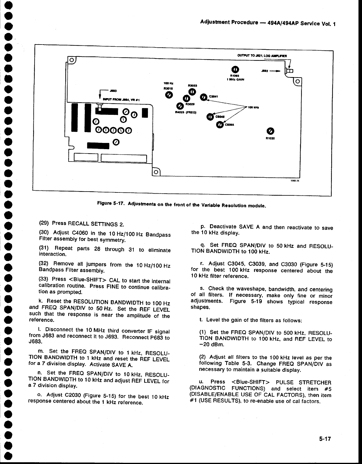
o
o
o
a
O
o
o
I
O
o
I
a
o
a
o
I
o
I
O
o
o
a
o
o
o
o
a
o
t
I
o
O
O
o
o
o
o
t
a
o
o
o
o
o
(29) Press
RECALL
SETTTNGS
2.
!30) Adjust C4060.
in the 10
Hzl100
Hz Bandpass
Filter
assembly
for
best
symmetry.
lgtt Repeat parts 2g through 31 to etiminate
interaction.
(32) Remove
ail jumpers from the 10 Hzl100
Hz
Bandpass
Filter
assembly.
(33) press <Btue-SHtFT>
CAL
to start
the internat
calibration
routine.
press FINE
to continu€
calibra_
tion as prompted.
K. RCSCT
thE RESOLUTION
BANDWIDTH
tO
1OO
HZ
and FREQ
SpAN/Dtv
to 50
Hz. set the REF
LEVEL
su-ch
that the response
is near the amplitude
of the
reference.
L Disconnect
the
10
MHz
third
converter
lF signal
from
J683 and
reconnect
it to J690. Reconnect
p6g3
to
J683.
m. set the FREQ
spAN/DlV
to 1
kHz,
RESOLU-
TION
BANDWIDTH
to 1 kHz and
reset
the REF
LEVEL
tor
a 7 division
disptay.
Activate
SAVE
A.
n. set th€ FREQ
spAN/DtV
to 10
kHz,
RESOLU-
TION
BANDWTDTH
to 10
kHz
and
adjust
REF
LEVEL
for
a
7 division
display.
o. Adjust
C2030
(Figure
5-1S)
for the best 1O
kHz
response
centered
about
the
1 kHz
reference.
Adjustnent Procedure
- 4g4[l4g4Ap Service
Vot.
1
p. Deactivate SAVE A and then reactivate to save
the 10
kHz display.
q. Set FREQ SPAN/D|V
to 50 kHz and RESOLU_
TION
BANDWIDTH
to 100 kHz.
, r. Adjust C3045, C3039, and C3030 (Figure 5_15)
for the best 100 kHz response centered about the
10 kHz filter reference.
s. Check the waveshape, bandwidth, and centering
of all filters. lf necessary, make only fine or minor
adjustments. Figure 5-1
g shows typical response
shapes.
t. Level
th€ gain of the filters as follows:
(1) SCt thE FREQ SPAN/DIV
tO
5OO KHZ,
RESOLU-
TION BANDWIDTH
to 1OO
KHz,
and REF LEVEL
to
-20 dBm.
(2) Adjust all filters to the 1OO
kHz tevet as p€r the
follovying
Table 5-3. Change FREQ SPANIDIV as
necessary
to maintain
a "suitable
display.
u. Press <Blue-SHtFT> PULSE STRETCHER
(DIAGNOSTIC FUNCTTONS)
and setect item #s
(DISABLE/ENABLE
USE OF CAL FACTORS),
then item
#1 (USE
RESULTS),
to re-enable
use of cal factors.
ocrttt? to.t2l, too ArLlEi
d @.*.'
@t* --;o,-.*
R'm3
GnEo'
66-//
6*@
oooo@
Figure 5-17. Adiu3tments on the front of the Variabte Resolution module.
5-17
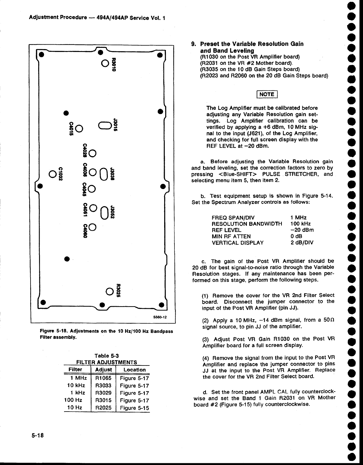
oOo
og
oo
$o o3
$o
oE EooE
a$o
go0F
go
o
o
,
oH
ooo
Adiustment Procedure
- 494A1494Ap
Service Vol. 1
Figure 5-18.
Adiustments
on the 10
Hzl100 Hz
Bandpass
Filter
assembly.
FILTER
Filter Locatlon
Preset the Variable Resolution Gain
and Band Leveling
(R1030 on
the Post VR
Amplifier
board)
(R2031
on
the
Va #2 Mother
board).
(R3035 on
the 10
dB Gain
Steps board)
(R2023 and
R2060 on
the
20
dB Gain Steps
board)
The Log Amplifier must be
calibrated
before
adjusting any Variable
Resolution
gain
set-
tings. Log Amplifier calibration can be
verified
by applying
a +6 dBm,
10 MHz
sig-
nal to the
input
(J621),
of the Log Amplifier,
and checking
lor full screen display
with
the
REF LEVEL at
-20 dBM.
a. Before adjusting
the Variable Resolution
gain
and band
leveling,
set
the
correction
factors
to zero
by
pressing <Blue-SHIFT> PULSE STRETCHER,
and
selecting
menu item
5, then
item
2.
b. Test equipment setup
is shown in Figure 5-14.
Set the
Spectrum
Analyzer
controls
as follows:
FREQ
SPAN/D|V
RESOLUTION BANDWIDTH
REF LEVEL
MIN RF
ATTEN
VERTICAL
DISPLAY
1 MHz
1 00 kHz
-20 dBm
0dB
2 dB/DrV
c. The gain of the Post VR Amplifier
should be
20 dB for best
signal-to-noise
ratio
through the
Variable
Resolution
stages. lf any maintenance
has been
per-
formed
on
this
stage,
perform
the
following
steps.
(1) Remove
the cover
for the VR 2nd
Filter
Select
board. Disconnect the jumper connector
to the
input
of the
Post VR Amplifier
(pin
JJ).
(2) Apply
a '10
MHz,
-14 dBm
signal, from a 50o
signal
source,
to pin
JJ of the
amplifier.
(3) Adjust Post VR Gain R1030
on the Post VR
Amplifier
board for a full
screen
display.
(4) Remove
the
signal
trom
the
input to the
Post
VR
Amplifier
and replace the iumper connector
to pins
JJ at the input to the Post VR Amplifier.
Replace
the
cover
for the
VR 2nd
Filter Select
board'
d. Set
the front
panel
AMPL
CAL
fully counterclock-
wise and set the Band 1 Galn
R2031
0n VR Mother
baard
#2 (Figure
5-15)
fully
counterclockwise.
1 MHz
10
kHz
1 kHz
100
Hz
10 Hz
Figure
5-17
Figure
5-17
Figure
5-17
Figure
5-17
Figure
5-15
o
o
o
o
o
o
o
a
o
o
o
a
o
a
o
o
o
t
o
a
o
o
a
o
a
o
a
O
o
o
o
o
a
o
I
o
a
o
o
o
o
o
a
a
9.
Table 5-3
5-18
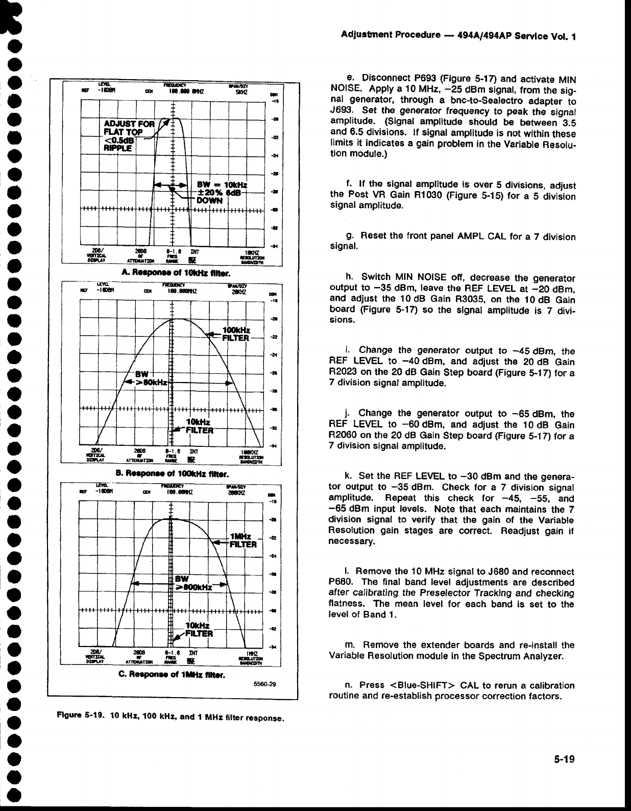
b,
-
O
O
o
I
o
I
o
I
o
I
O
o
o
I
o
t
o
o
o
o
o
o
o
o
o
o
I
O
a
a
o
o
o
o
I
o
o
o
o
o
o
o
Adjurtment Procedure
- 494A1494Ap
SeMce Vot.
I
e. Disconnect
p693
(Figure
5-17)
and
activate
MtN
NOISE.
Apply
a 10
MH4 -25 dBm signat,
from
the sig-
nal generator, through a bnc-to-sealsctro
adapter to
J693: Set the genorator
frequency
to peak the signal
amplitude. (Signal
amplitude
should
be between
3.5
and
6.5
divisions.
tf signal
amptitude
is not
within
these
limits
it indicates
a gain
problem
in
the Variable
Resolu-
tion
module.)
f. lf the signal
amplitude
is over
5 divisions,
adjust
the Post
VR Gain R1030
(Figure
5-15) for a 5 diviiion
signal
amplitude.
g. Reset
the front
panel
AMPL
CAL for a 7 division
signal.
h. Switch
MIN NOISE
off, decrease
the g€nerator
output
to -35 dBm,
leave
the REF
LEVEL
at -20 dBm,
and
adjust
the 10dB Gain
R303S,
on the 10dB Gain
board (Figure
5-17)
so the signal
amptitude
is 7 divi-
sions.
i. Change the generator output to -4S dBm, the
REF LEVEL
to -40 dBm, and adjust
the 20 dB Gain
R2023
on the 20 dB Gain
Step board
(Figure
5-17) for a
7 division
signal amplitude.
j. change the generator
output to -65 dBm, the
REF
LEVEL
to -60dBm, and adjust
the t0dB Gain
R2060
on the 20 dB Gain
Step board
(Figure
5-1Tl tor a
7 division
signal
amplitude.
k. set the REF
LEVEL
to -30 dBm
and
the
genera-
tor output
to -35 dBm. Check
lor a 7 division
signal
amplitude. Repeat this check for -45, -55, and
-65 dBm input levels. Note
that each maintains
the Z
division
signal
to verify
that the gain of the Variable
Resolution
gain stages
are correct. Readjust
gain il
necessary.
l. Remove
the 10
MHz
signal
to J680
and
reconnect
P680. The final
band
level
adjustments
ar€ described
after calibrating
the Preselector
Tracking
and checking
flatness. The mean level
for each band is set to th€
level
of Band 1.
m, Remove
the extender
boards
and re-install
the
Variable
Resolution
module
in
the Spectrum Analyzer.
n. Press <Blue-SHIFT>
CAL
to rerun a calibration
routine
and re-establish
processor
correction
factors.
E -loil
ro.a attr
(Ex re.&ra
q lo.dtla
TT
-ll
a
a
.A
-t
-t
{
{
*
n
-ta
a
-a
-ar
-a
.,
{
-e
{
GI.E
fEo lqlfl
EL[rn
lrrccDil
D{T
B
TI
-tl
€
-4.
-ca
€
-a
{
d
-t.
ut
rlrngt
08tr
f" Rrynm ot tqOE filtrr.
B. Rorpolrrc oil lolrlls fft r.
tl
. ilqdr
EFILTER
\t I
_1
/ arrl
F,>Ai kHr
\
/rl
lOtHz
I
lilllz -
FILTER
\
EUI
>!oot(Hi-{
I\I
I-Jn
"J
,.T"*r\
C. Rcrpoor ot tn|z fihcr. 55@-29
Flgurc 5-19. 10 kHz, 100 kH:" and 1 MHz lilter response.
5-19
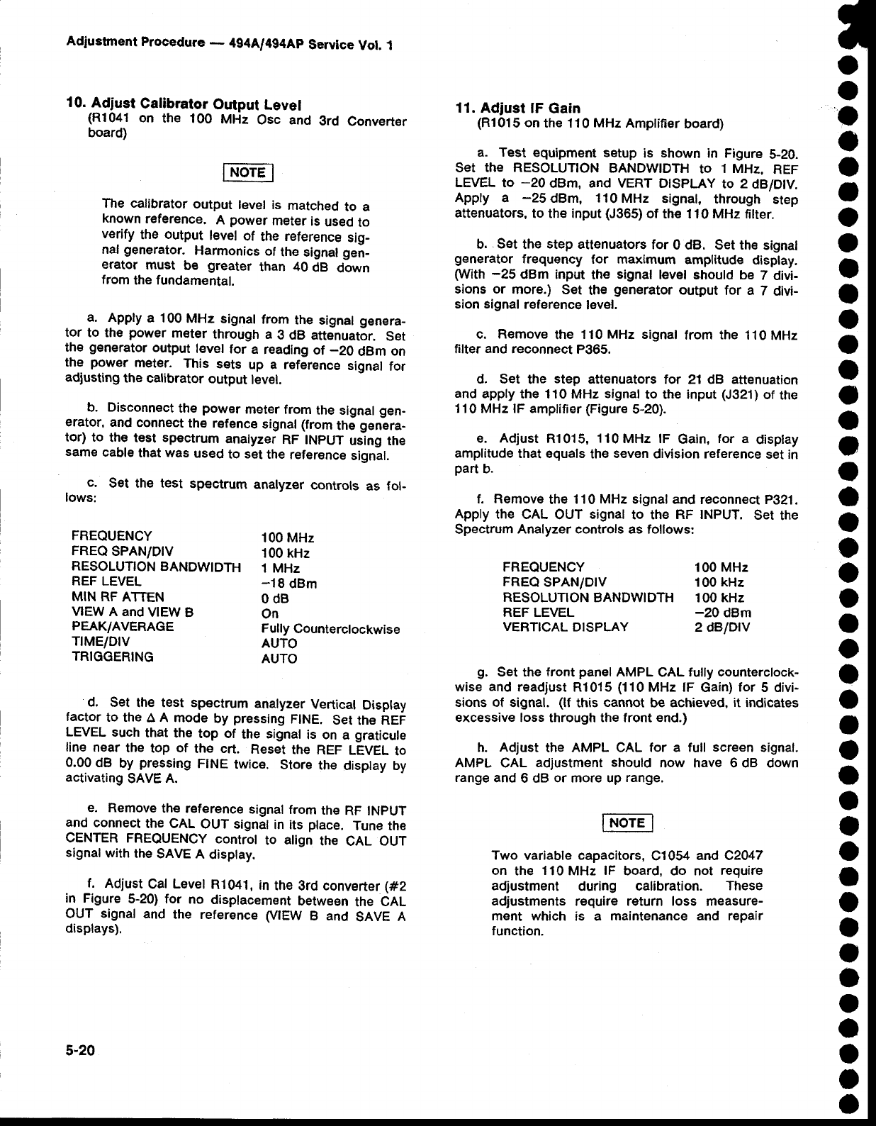
Adiustment
Procedure
- 494A/4g4Ap
Service
Vot. 1
10.
Adjusf
Calibrator
Output
Level
(R1041
on the 100 MHz
Osc and
3rd Converter
board)
The calibrator
output level is matched
to a
known
reference.
A power
meter
is
used
to
verify
the output
level
of the
reference
sig_
nal
generator.
Harmonics
of th€
signal gen_
erator must be greater
than 40
dB down
from
the fundamental.
a. Apply
a 100
MHz signal
from
the signal g€nera_
tor to the power
meter
through a 3 dB attenuator.
Set
the generator
output
level
for a reading
of -20 dBm
on
the power
meter. This sets up a reference
signal
for
adiusting
the calibrator
output
level.
b. Disconnect
the
power
meter
from
the signal
gen-
erator,
and
connect
th€ refence
signal
(from
the
genera-
tor) to the
test spectrum
analyzer
RF INPUT
using
the
same
cable
that was used
to set
the
reference
signal.
c. Set the test spectrum analyzer
controis as fol_
lows:
11. Adjust lF Gain
(Rl015
on
the 110
MHz
Amptifier
board)
a. Test equipment setup
is shown
in Figure
5-20.
SEt thE RESOLUTION
BANDWIDTH
tO 1 MHZ, REF
LEVEL
to -20 dBm, and VERT
DISPLAY
to 2 dB/DtV.
Apply a -25 dBm, 110
MHz signat, through step
attenuators,
to the
input
(J365)
of the 110 MHz
fitter.
b. set the step
attenuators
for 0 dB. set the
signal
generator frequency {or maximurn amplitude display.
With -25 dBm input
the signal
level
shoutd be 7 divi-
sions or more.) Set the generator
output
for a 7 divi-
sion signal
reference
level.
c. Remove
the 110
MHz
signal
from
the 110
MHz
filter
and
reconnect
P365.
d. Set the step attenuators for 21
dB attenuation
and
apply
the 110 MHz
signal
to the input
(J321)
of
the
'110
MHz lF amplifier (Figure
5-20).
e. Adjust
R1015,
110
MHz lF Gain,
for a disptay
amplitude
that equals
the
seven
division reference
set
in
part b.
f. Remove
the
110
MHz
signal and
reconnect P321.
Apply
the cAL ouT signal
to the RF |NPUT. set the
Spectrum
Analyzer controls as
follows:
FREQUENCY 100 MHz
FREQ
SPAN/DIV 100
kHz
RESOLUTION
BANDWIDTH 100 kHz
REF LEVEL -20 dBm
VERT]CAL
DISPLAY 2 dB/DIV
g. Set the front panel AMPL CAL fully counterclock-
wise and readjust Rl015 (110
MHz lF Gain)
for 5 divi-
sions of signal. (lf this cannot be achieved, it indicates
excessive loss through the front end.)
h. Adjust the AMPL CAL for a full screen signal.
AMPL CAL adjustment should now have 6 dB down
range and 6 dB or more up range.
Two variable
capacitors,
C1054
and C2047
on the 110
MHz lF board, do not require
adjustment during calibration. These
adjustments
require return loss measure-
ment which is a maintenance and repair
function.
o
o
O
o
O
o
o
o
a
a
a
a
o
o
o
o
a
o
o
o
o
o
o
o
o
o
o
o
I
o
O
o
o
o
a
o
a
o
a
o
o
o
FREQUENCY
FREQ
SPAN/D|V
RESOLUTION
BANDWIDTH
REF
LEVEL
MIN RF
ATTEN
VIEW
A and
VIEW B
PEAK/AVERAGE
TrME/DtV
TRIGGERING
100 MHz
100 kHz
1
MHz
-18 dBm
0dB
On
Fully
Counterclockwise
AUTO
AUTO
d. Set the test spectrum
analyzer
Verticat
Display
factor
to the
A A mode
by pressing
FINE. Set
the REF
LEVEL
such
that
the top of the signal
is on a graticule
line near
the top of the crt. Reset
the REF
LEVEL
to
0.00
dB by pressing
FINE
twice. Store
the display by
activating
SAVE
A.
e. Remove
the
r€ference
signal
from
the
RF
INPUT
and
connect
the cAL oUT signal
in its place,
Tune the
CENTER
FREQUENCY
controt
to atign
the CAL OUT
signal
with
the
SAVE
A disptay.
f. Adjust
Cal
Levet
R1041,
in the
3rd converter
(#2
in Figure
5-20) for no displacement
between
the CAL
OUT signal
and the reference
(VIEW
B and SAVE
A
displays).
5-20
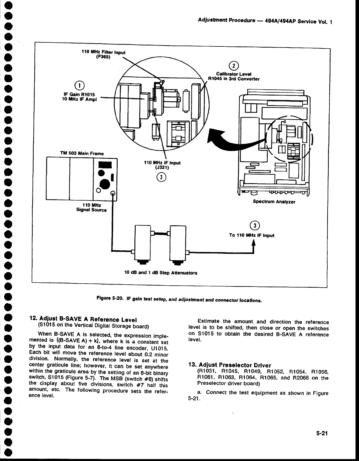
o
o
o
a
o
o
O
I
o
a
I
a
a
o
t
t
t
I
o
o
O
o
o
o
o
o
a
o
I
o
o
o
I
o
o
o
o
I
I
o
o
t
I
a
Adjustment
procedure
- 4g4Al4g4Ap
seMce vot. 1
Figure
5-20- lF gain
test setup,
and adjustnent and
conn€ctor
rocason3-
12.
Adjust B-SAVE A Reference Level
(S1015
on
the
Verticat
Digitat
Storage
board)
when B-sAVE
A is selected,
the expression
imple-
mented
is (B-sAVE
A)
+ kl, where
k is'a constant
set
by the input data for an g-to-4
line encoder,
u1015.
Each
bit will move
the reference
level
about
0.2
minor
division. Normally,
the reference
level is set at the
center graticule
line;
however,
it can be set anywhere
within
the graticute
are3
!y the setting
of an g_bii
binary
switch,
S1015
(Figure
5-7). The
MSB (switch
#8) shifti
the display
about five divisions,
swiich #7 h;lf this
amount,
etc. The following
procedure
sets the refer-
ence
level.
Estimate
the amount and direction
the reference
level
is to be shifted,
then close or open
the switches
on 31015 to obtain
the desired
B-SAVE
A reference
level.
13. Adjust Preselector Driver
(Rl031, Rl045, Rl049, Rl052, R10s4,
Rl056,
R1061,
R1063,
R1064,
R1065, and R2066
on the
Preselector
driver board)
a. Connect
the test equipment
as shown in Figure
5-21.
Calibrato. Level
R1045 in 3rd Converter
lF Gain R1015
10 ltlHz lF Ampl
Tll 5O3
llain Frame
10 dB and 1 dB Step Attenuators
5-21
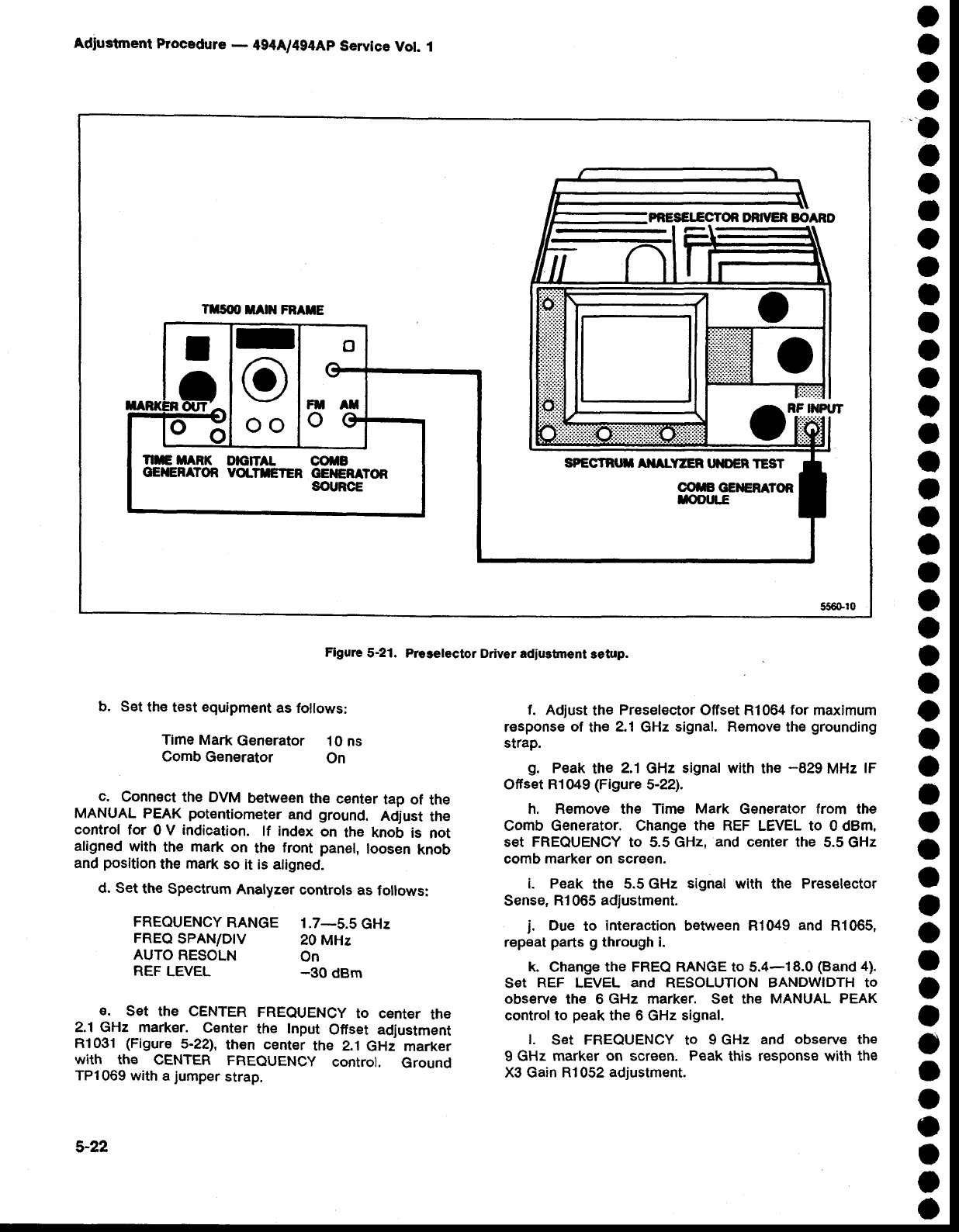
Adlustment
Procedure
- 494A/494Ap
Servlce
Vot. 1
Figure
5-21. Preselector
Driver adiustment
lietup.
o
a
o
o
o
o
o
I
o
o
I
a
a
a
I
o
o
)
o
a
o
o
a
O
o
o
o
o
t
o
o
a
O
O
O
o
o
o
o
o
I
o
o
o
b. Set
th€
test equipment
as follows:
Time Mark
Generator .l
0 ns
Comb
Generator On
c. Connect
the DVM between
the center
tap of the
MANUAL PEAK
potentiometer
and
ground. Adjust
the
control
for 0 V indication.
lf index
on the knob is not
aligned
with the mark
on the front panel,
loosen
knob
and
position
the
mark
so it is aligned.
d. Set
the Spectrum
Analyzer
controls
as follows:
FREQUENCY
RANGE 1.7-5.5 GHz
FREQ
SPAN/D|V 20
MHz
AUTO
RESOLN On
REF
LEVEL _30 dBm
E. SEt thE CENTER
FREQUENCY
tO CENIET
thE
2.1 GHz markEr. Center the Input Ofiset adjustment
R1 031 (Figure
5-221,
then center
the 2.1
GHz marker
with the CENTER FREQUENCY
control. Ground
TP1069 with
a
jumper
strap.
f. Adjust
the Preselector Offset Rl064
for maximum
response
of the 2.1
GHz
signal. Remove
the
grounding
strap.
s. Peak
the 2.1
GHz
signal with the -829 MHz lF
Ofiset R1049
(Figure
5-22).
h, Remove the Time Mark Generator from the
comb Generator. change the REF LEVEL to 0 dBm.
set FREQUENCY
to 5.5 GHz, and center
the 5.5
GHz
comb
marker
on screen.
i. Peak the 5.5 GHz signal with the Preselector
Sense,
R1
065
adjustment.
j. Due to interaction
between R1049
and R1065,
repeat
parts g through i.
k. change
the FREQ RANGE
to 5.4-18.0 (Band
4).
S€t REF LEVEL and RESOLUTION BANDWIDTH
to
obsgrve
the 6 GHz marker. Set the MANUAL
PEAK
control to peak
the 6 GHz signal.
l. Set FREOUENCY
to 9 GHz and observe
th€
9 GHz
marker on screen. Peak
this response
with the
X3 Gain
Rl052 adjustment.
PRESEIECTON OR]YER EOARD
Ttrsoo
MAN
FRATE
OTi#i"
SPECTRT I AilALYZER lrl'DER TEST
OMGEilERATOR
f,OOIJLE
Io
oo
NETARK DIGITA OOTB
GilERffOR VOLTreTER GEilERATOR
SOURCE
5-22
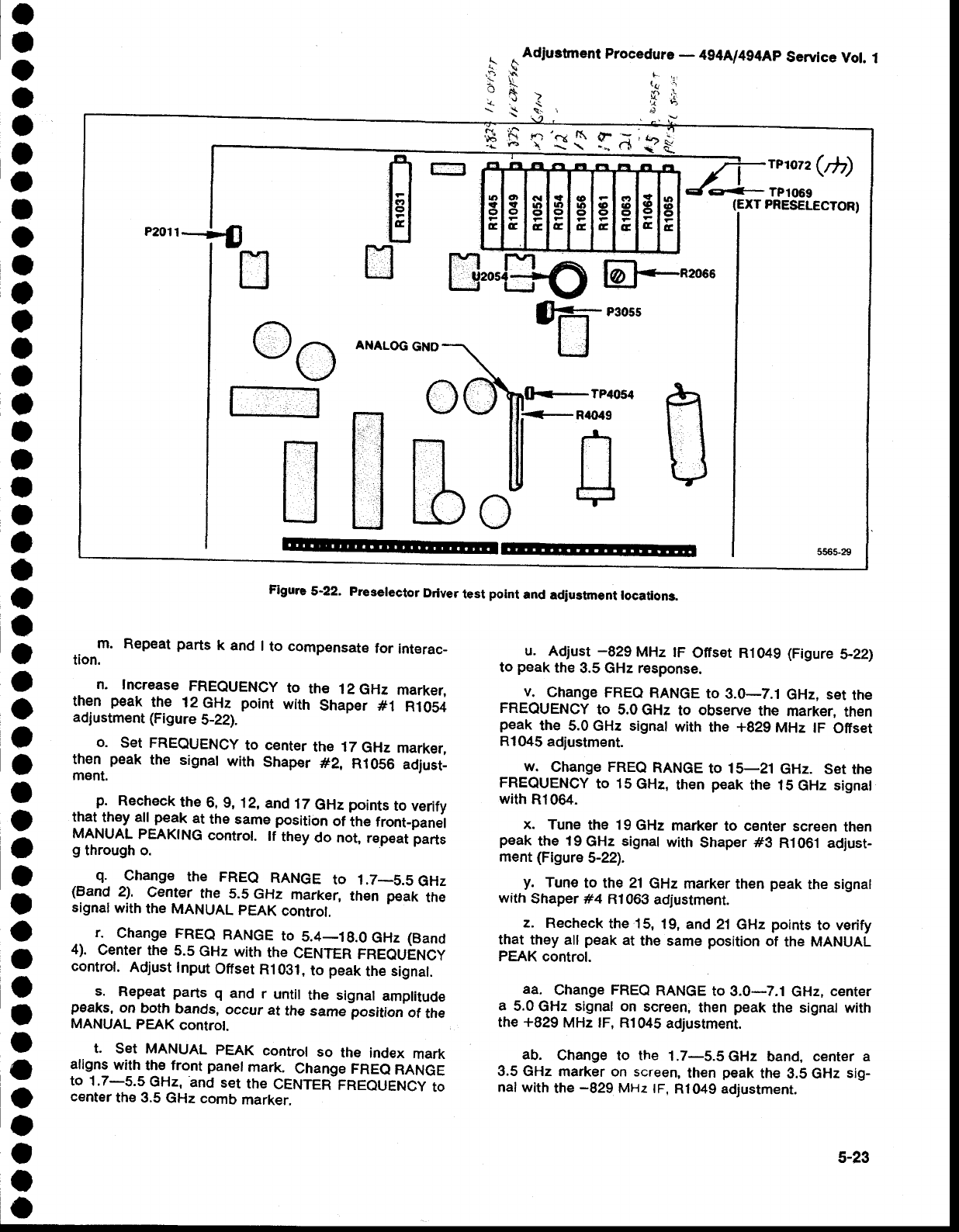
o
I
o
o
O
O
o
I
o
O
o
I
a
a
o
o
t
a
a
o
o
o
o
o
a
o
a
O
I
o
a
o
I
a
o
o
I
t
o
o
a
I
a
a
o
{
A
Adrustment
Procedure
- 4g4A/494Ap
Service
Vol. l
$tsr.
h - 1,",1
';'i 1'[
\\\-''l
Figurc
5-22. Preselector
Driver
test point
and adiustment
locations.
. m. Repeat
parts
k and
I to compensate
for int€rac_
tion.
n. lncrease
FREQUENCY
to the 12GHz marker,
then peak the 12
GHz point with Shaper #1 R1OS4
adjustment
(Figure
5-22).
o. Set FREeUENCY
to center
the 17
GHz
marker,
then peak the signat
with Shaper
#2, R1056
adjust_
ment.
p. Recheck
the
6,9, 12,
and
17
GHz
points
to
verify
that
th€y all
peak
at the
same
position
or
tne rront_panet
MANUAL
PEAKING
control. lf they
do not,
repeat parts
g through o.
_ q. Change the FREQ RANGE to 1.7_5.5 GHz
(Band
2). Center
the 5.5
GHz marker,
then peak
the
signat
with
the
MANUAL
PEAK
control.
r. change FREQ
RANGE
to 5.4_19.0
GHz
(Band
4). Center
the 5.5
GHz
with
the
CENTER
FREQUiNCY
control.
Adjust
Input
Offset
R10gl,
to peak
the signat.
:. Repeat
parts q and r untit
the signat
amptitude
peaks,
on both bands,
occur
at the same position
of the
MANUAL
PEAK
controt.
t. Set MANUAL
pEAK control
so the index
mark
aligns
with
the
front
panel
mark. Change
FREQ
RANGE
tO 1.7_5.5 GHZ,
ANd
SEt
thE
CENTER
FREQUENCY
tO
center
the 3.5
GHz
comb
marker.
u. Adjust
-829 MHz tF Offset Ri049 (Figure
5-22)
to peak
the
3.5 GHz response.
v. Change
FREQ
RANGE
to 3.0-7.1 GHz,
set
the
FREQUENCY
to 5.0 GHz to observe
the marker,
then
peak the 5.0 GHz signat
with the +829
MHz tF Offset
R1045
adjustment.
w. Change FREQ
RANGE
to 15-21 GHz. Set
th€
FREQUENCY
to 15GHz,
then
peak
the t5GHz signal
with
Rl064.
x. Tune
the 19
GHz
marker
to c€nter
screen
then
peak
the 19
GHz
signal
with Shaper
#3 R1061 adjust-
ment
(Figure
5-22).
y. Tune
to the 21
GHz marker
then
peak
the
signal
with
shaper #4 n1063
adjustment.
z. Recheck
the 15,
19, and 21
GHz
points
to verify
that they
all peak
at the same
position
of the MANUAL
PEAK
control.
aa. Change FREQ
RANGE
to 3.0-7.1 GHz,
center
a 5.0
GHz signal on screen;
then
peak
the signal with
the
+829
MHz lF,
Rl045
adjustment.
ab. Change
to the 1.7-5.5 GHz band, center a
3.5 GHz
marker on screen,
then
peak
the
9.5 GHz
sig-
nal with
the
-829 MHz
tF,
Rl049 adjustment.
.f\ ,r) r
I r;;3
H
H
[:r p-rplo?2(/h)
& TP1069
(EXT
PRESELECTOR)
n
oo
r-
[,*f4n ldFnzo'e
ANALOG GND fi"**
Qr
B
TP'O54 n
ilHc
R.|{}49
il
5-23
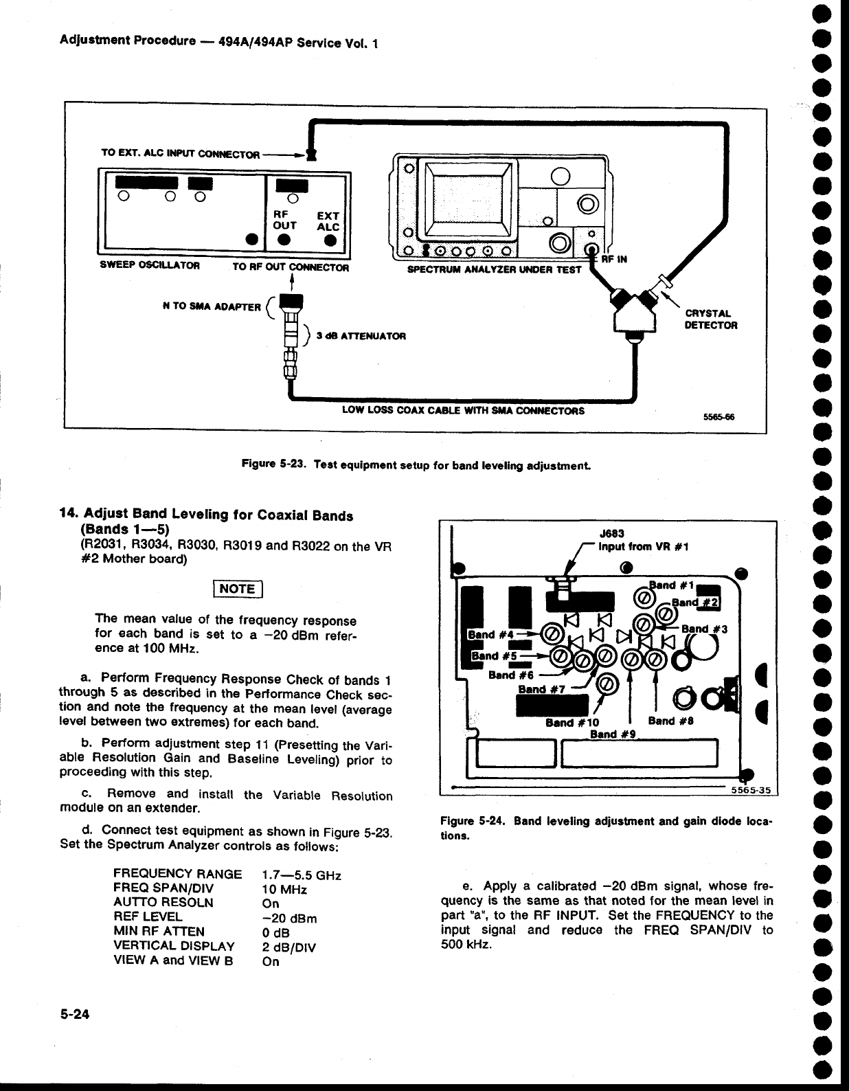
Adfustrnent
Procedure
- 4g4A/4g4Ap
Servtce
Vol. 1
o
I
o
a
o
o
o
t
o
a
I
t
O
O
o
o
a
t
o
a
a
o
a
O
a
o
o
o
O
o
a
o
t
o
o
o
I
o
o
o
o
o
o
o
Figure
5-23. Test
equipment
setup for band
leveling
adiustmenl
1tt.
Adjust Band Leveting
lor Coaxial
Bands
(Bands
1-5)
(R2031,
R3034,
R3090,
R9019
and
R3022
on
the
VR
#2 Mother
board)
The mean value
of the frequency
response
for each band is set to a -20 dBm refer-
ence at
100 MHz.
a. Perform
Frequency
Response
Check of bands 1
through
5 as described
in the performance
Check sec-
tion and note th€ frequency
at the mean
level (average
level
between
two extremes)
for each
band.
b. Perform
adiustment
step 11
(presetting
the
Vari-
able Resolution
Gain and Baseline
Leveling)
prior to
proceeding
with
this
step.
c. Remove and install the Variable Resolution
module
on an
extender.
d. Connect test
equipment
as shown
in
Figure
5-23.
Set the
Spectrum Analyzer
controls
as
follows:
FREQUENCY
RANGE 1.7-5.5 GHz
FREQ
SPAN/D|V 10
MHz
AUTTO
RESOLN on
REF
LEVEL -20 dBm
MIN
RF ATTEN O dB
VERT|CAL
DTSPLAY 2 dB/Drv
VIEW
A and
VIEW
B on
5-24
Inpul trom VR
#1
I
I
Figure 5-24.
Band leveling adiustment
and
gain
diode loca-
tion3.
e. Apply a calibrated
-20 dBm signal,
whose fre-
quency
is the same
as that noted for the mean
level in
part 'a",
to the RF INPUT. Set
the
FREQUENCY
to the
input signal and reduc€ the FREQ SPANIDIV to
500 kHz.
TO EXT. ALC IXP|JT@}|IGCTOR-
Ioo Ioro
RF EXT
OUT ALc
ot oo
sttEEP osc|llATOR TO RF OUT @IOIECTON
ISPECTRUT AIIALY:ZER ITIOER TEST
LOW
LOSS
COAX
CABI."E WttH SflA OO|,{€CTORS
a
I
o
o
o
o
o
I
o
o
o
t
o
t
o
I
I
I
o
a
a
o
o
o
o
o
t
o
o
O
a
o
o
a
o
o
I
t
o
o
a
o
o
o
. f. Adjust Band 2 Gain RgOg4
on th€ vR Mother
b.oard #2 (Figure 5-241
tor a fult screEn
(_20
OBml
display.
_ g. Chang€
th€ FREQUENCY
RANGE
to 3.0_
7.1
GH.z
(Band
3) and
appty
a catibrated
_20
dBm sig-
nal
with
the same
frequency
as noted
for the
mean
level
in Band
3 for part a of this step.
h. set the FREQUENCy
to the
incoming
signat
and
FFEO
SPAN/DIV
to 500
kHz/Div
i. Adjust
Band
3 Gain
R3030
(Figure
5-24)
for a futl
screen
display.
j. Repeat the above procedure for €ach coaxial
band (1-5) and set the gain of each
with the appropri-
ate adjustment. lf the range of any adjustmEnt
is
insufficlent,
add
or r€move
a diode
betrr,leen'pin
DD
and
th€
-appfopriate
adjustment
potentiometer
on th€ vR
Mother board #2. to obtain the reguired
range. Refer
19 .th: schematic
diagram
and component
tocator
for
Variable Besolution Mother goarOs, in Volume 2.
Adding
the
diode
increases
gain.
15. Adiust Band Leveling for Waveguide Bands
(Bands
6-11)
(R3024,
R3026,
Rg02g, R9029,
anct
R3032
on the
VR
Mother
board
#Z)
?. I:g! equipment
setup is shown
in Figure
5-23.
Apply 2072
MHz at -€O dBm, through a dt_btocking
capacitor
to the EXT MIXER input. Monitor the inpui
with a pow€r meter to set the pow€r tevel
then add a
known 30
dB attenuator so th€ input level to the
EXTERNAL
MIXER
port is -60 dBm. 'Set
ttre
Spectrum
Analyzer
controls
as
follows:
FREQUENCY
RANGE 1g_26 GHz
(Banct
6)
FREO
SPAN/D|V 200
MHz
AUTO
RESOLN On
REF
LEVEL -3OdBm
The baseline
of the display
will rise
when
the 2072
MHz signat is apptied to the
EXTERNAL
MTXER
input
port
connector.
b. With
-60 dBm input
level
apptied,
adjust
Bancl
6
Gain Leveting
R3024 (Figure 5-24) lor iuil screen
display.
c. change
the FREQUENCY
RANGE
and
input
sig-
nalfrequency
and
level
as
listed
in
Table
54, and
adjuit
the appropriate
Band
Gain
adjustments
for a fult screen
display.
Gain
adjustment
for
the waveguide
bands
need
to be adjusted
only
if these
bands
will
be used.
d. Switch
POWER
off; replace
Variable
Resolution
module,
then
switch
POWER
back
on.
Adru3tment
Procedure
- 4g4rl4g4Ap Service
Vot.
I
Tabte
5-4
EXT
MIXER
BAND
LEVELING
ADJUSTi,IENTS
Band Gain
AdJustment
6 (18-27 GHz)
7 (26-40 GHz)
8 (33-60 GHz)
9 (50-90 GHz)
10
(75-140 GHz)
11
(110-220 GHz)
12
(r7O-325 GHz)
R3024
R3026
R3032
R3029
R3028
R3028
R3028
16.
Phase
Lock Calibration
(C1016,
C1018,
C1032, and
C1034
on
the
Strobe
Driver
board;
C10i3 and C2011
on th€ Controlled
Oscillator
board;
and Rl06l and R3Og2
on the Error
Amplifier
board)
The
Phase
Lock
assembly
normally
requires
calibra-
tion only after some part of the assembly
has been
repaired
or replaced. phase noise, produced
by the
phase lock loop, is specified
tor -7AdBc or better,
3 kHz out from the response.
This should
be checked
before
calibrating
th€ assembly.
a. Test equipment
setup is shown
in Figure
5-25.
Remove
the Phas€ Lock module and the two cover
plates so all circuit test points and adjustm€nts
are
accessible.
Plug
the assembly
on extender
boards
and
into
the instrument.
Use
Extender
cables
and
adapters
to reconnect
signal
cables
to their respective
connector
(cable
with yellow band to J501, and the cable
with
black
band
to J502).
lf d€sired, the direct reading
counter may be con-
nected
to the Vertical
Output of the t€st oscilloscope
to
get a count of a display at each test point, when
appropriate,
throughout
this procedure. The ground
side of the test oscilloscope
probe will serv€
as the
common ground
return
for
both
instruments.
b. Press <Blue-SHIFT>
CAL and do the directed
calibration
routine through adjusting
the LOG CAL.
Press <Blue-SHIFT>
to return
the instrument
to nor-
mal
operation
and
set REF LEVEL
to -30 dBm. Check
that the AUTo RESoLN
is active (button
tit).
c. Check O{fset Mixer - This part of the pro-
cedure
is only required
after repair
or replacement
of
the
Mixer
board.
(1) Connect the Direct Input of the frequency
counter to pin N (Figure
5-26) and set the counter
controls
for a count. Note
the
frequency.
(2) Connect
the counter
to pin K and note
the
fre-
quency.
5-25
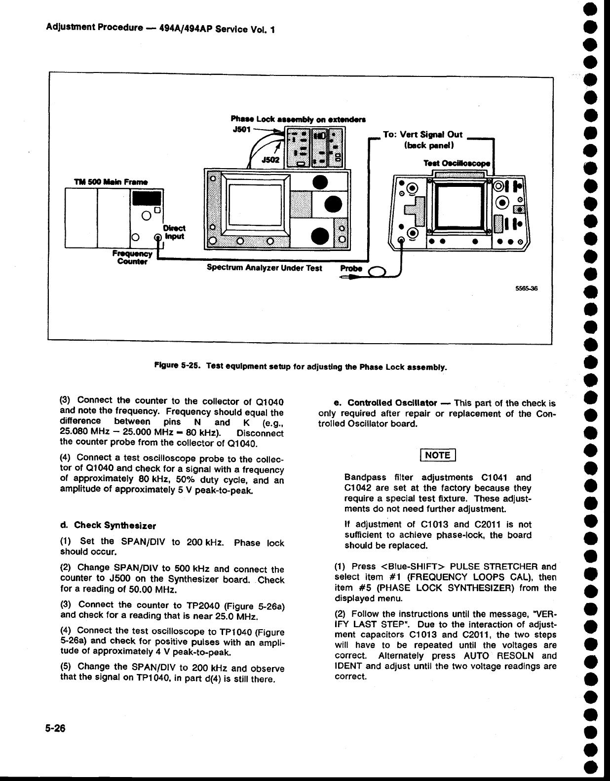
AdJustnent
Procedure
- 494A/4g4Ap
Servtce
Vot. I
To: Vsrt liignel Out
(back penell
Spectnrm
Analyrer Under Tegt
Flgure
5-25. Test equlpm€nt
retup for adjusting
llre phase
Lock assembly.
o
a
o
o
o
o
o
,
a
a
o
I
a
I
o
a
t
I
o
o
o
I
a
a
o
a
o
o
o
o
o
a
t
O
o
o
o
o
o
o
o
o
o
O
(3) Connect
the counter to the coll€ctor of e1040
and
not6 the frequency. Frequency
should
equal
the
difference between pins N and K (e.g.,
25.080
MHz
- 25.000
MHz
- 80
kHz). Disconnect
the
counter
probe
from
the collector
of e1040.
(4) Connect a test oscilloscope
probe
to the collec-
tor of Q1040 and
check
for
a signal
with
a frequency
of approximately
B0 kHz, 507" duty cycle, and an
amplitude
of approximatety
5 V peak-to-peak.
d. Check Synthesizer
(1) Set the SPAN/D|V
to 200
kHz. phase tock
should
occur.
{2) Change
SPAN/DIV
to 500
kHz and connect
the
counter
to J500 on the Synthesizer
board. Check
for
a reading
of 50.00 MHz.
(3) Connect
the counter to Tp2O40 (Figure
5_26a)
and
check
for a reading
that
is near
25.0
MHz.
(4) Connect
the
test oscilloscope
to Tpl040 (Figure
5-26a) and check for positive
pulses with an ampli-
tude of approximately
4 V peak-to-peak.
(5) Change
the SPAN/DIV
to 200
kHz and observe
that
the signal
on
Tpl040,
in part
d(4) is stiil
th€re.
G. Contolled Osc{llator
- This part of the check
is
only requirgd after repair or replac€ment
of the Con-
trolled Oscillator board.
Bandpass filter adjustments
c1041 and
C1042 are set at the factory because they
require
a special
test fixture. These adjust-
ments
do not
need further adjustm€nt.
lf adjustment of C1013
and C2011
is not
sufncient
to achieve
phase-lock,
the board
should
be
replaced.
(1) Press
<Blue-SHIFT> PULSE
STRETCHER
and
select item #1 (FREQUENCY
LOOPS
CAL), then
item #5 (PHASE
LOCK SYNTHESIZER)
from the
displayed menu.
(2) Follow
the
instructions
until
the
message,
'VER-
IFY LAST
STEP'. Due to the interaction
of adjust-
ment capacitors
C1 013 and C201
1, the two steps
will have to be repeated until the voltages are
correct. Alternately press AUTO RESOLN
and
IDENT
and adjust
until the two voltage
readings are
correct.
5-26
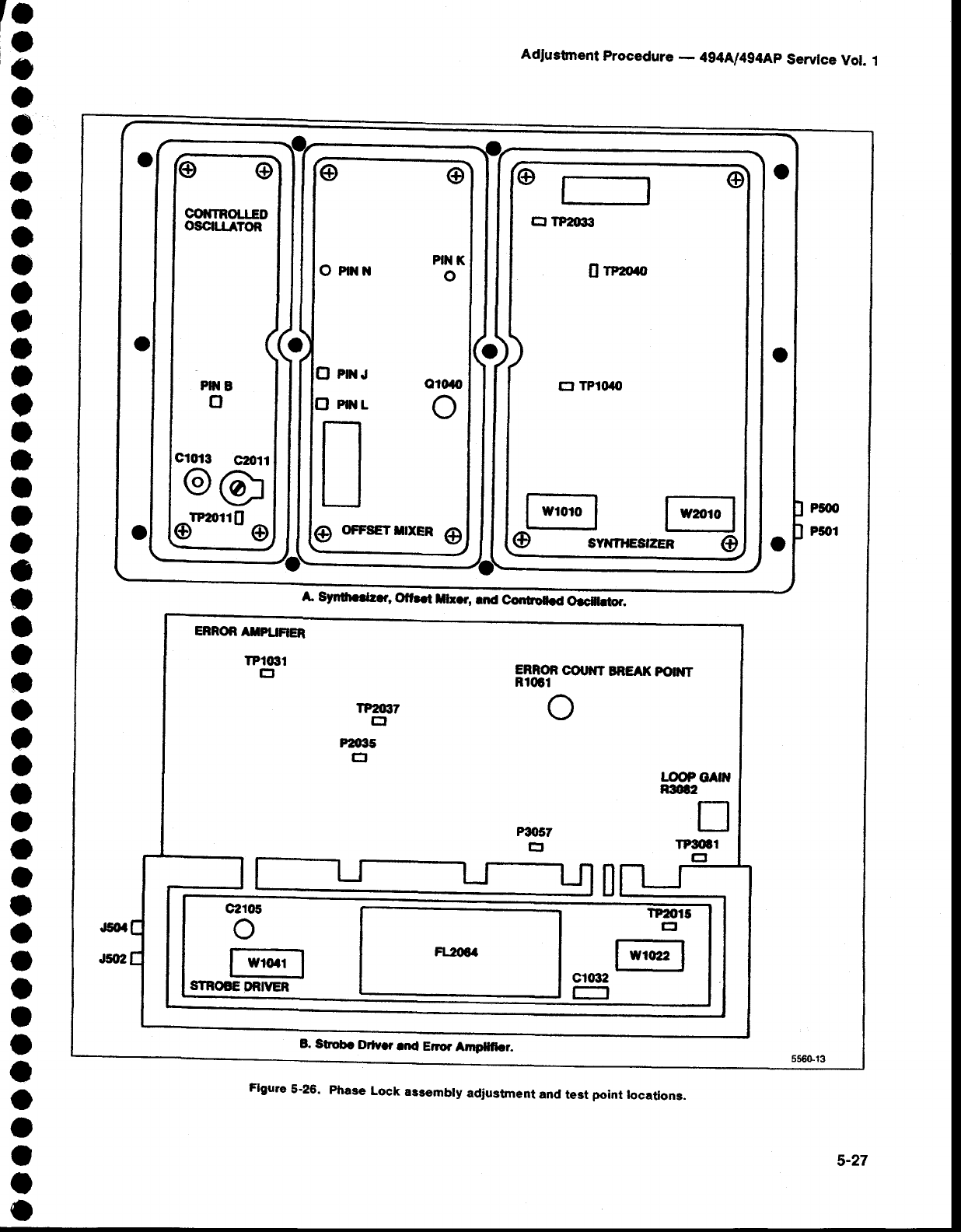
0@
coitrnou.ED
OSCIIIATOR
PSI
B
o
c1013 c,rll
@@r
o*tto @
(E
J-ffi] @
@ snrnasrzen @
l-r
rP2C3
E
rpzoro
El TP10'|O
@
Cf
0 put.l
El Ptilt-
L-J
@ oFFsE
nrxEn @
A Syntfredror, Oftrrt l|h.r, rnd Gontlotocl Orcileor.
LOOPOA0T
R30!2n
TP36T
E
TP,OI5
EI
| "trrl
c2105
o
fTr.t I
STROBE
DRIVER
Ft 004
B. Stiobc Orlyrr rnd Eror Ampllllcr.
Adrustment
Procedure
- 4g4A/4g4Ap
Servlce
Vol. 1
l.
t
a
o
o
a
o
I
o
I
o
I
o
I
I
I
I
a
t
a
a
o
a
o
I
o
o
o
o
a
a
a
I
o
o
a
I
I
o
o
o
I
o
o
Flgure 5-26. Phage Lock ariembly adjustment and test point locations.
Adiustment
Procedure
- 494A/tg4Ap Service
Vol. 1
(3) Connect the counter to Tp2o11 on th€ con-
trolled Oscillator board (Figure 5-26a) and atter-
nately
press
AUTO
RESOLN
and
IDENT
and
check
for a count reading of either 25.0g4g
MHz or
25.0328
MHz.
f. Chec-k
Opera0on of Strobe
Drlver
The *Phase
Lock Synthesiz€r"
test is still used
for
this test. lf aborted, press <Blue-SHtFT> PULSE
STRETCHER
to return to the Synthesizer routine. Any
step in
the routine
willwork.
(1) Connect the
test osciltoscope
to Tp2015
on the
Strobe Driver
board (Figure
5..26b)
and eheck
for a
square wave response with a Time/Div setting of
.05 ps. Amplitude
should
be ==5
V peak-to-peak.
(21 Connect the test osciiloscope to Tp2Og7 and
check for a sinusoidal waveform of approximatety
5vpp.
(3) lf the amplitude
of the strob€ signat
is low and
noisy, chang€
the values
of select capacitors
Cl01 6,
C1018,
C1032,
and
C1034
for maximum
amptitude
and
minimum noise
at TP2087. The
range
of values
for
these
capacitors
is 3.3
pF-27 pF.
(4) Connect th€ counter to TP2087 and check for a
count of either
5.018868
or 5.00642 MHz.
(5) Gonnect the
test oscilloscope
to JS04
and
check
for5Vlogiclevels.
(6) Press <Blue-SHIFT>
to abort the
test.
g. Error Ampllfier
- This procedure
sets
loop
gain
which
is required
when
either
the
Phase
Lock assembly,
1st
LO, Phase
Detector,
or Error
Amplifier is replaced.
(1) Set SPAN/DIV
to 200
kHz then press <Btue-
SHIFT> PULSE
STRETCHER.
The DTAGNOSTTC
FUNCTIONS
menu will now be disptayed.
Setect
menu
item
3 (DIAGNOST|C
A|DS)
and
setect
t st LO
PHASE LOCK (sub-menu item 0). phase tock
should
bs disabled.
(2) Connect the test osciiloscope
to Tp203B (Figure
5-26b) and set the test osciltoscope
Time/Div
to
20 ms. Check for a waveform
with an amplitude
that is approximately
6 V peak-to-peak.
(3) Press
lOdBiDlV
to enable
phase
lock
and note
that the message
indicates
LOCK ENABLED.
Con-
nect the test oscilloscope
to Tp 3081
(Figure
5-26b)
and vary R3082 from stop to stop and note
that the
beat
note signal
varies
in amplitude.
Press
<Blue-
SHIFT>
to return
to normal
op€ration.
(4) Set th6 TIME/DIV to AUTO, FREOUENCY
RANGE
to 1.7-5.5 (Band 2), and SpAN/D|V to
50
kHz.
(5) Remove
P3057
(Figure
5-26b). This
turns on the
strobe
to the Phase
Gate. Set Loop Gain
R3082
fully
counterclockwise. Move
P2035 to pins
2 and
3.
(6) Monitor TP3081 with the test oscllloscope.
Trigger
the test oscilloscope externally with
the
sig-
nal at TP2037 (U204&6)
shown Figure 5F26b. Set
the
test
oscilloscope Time/Div
to 5 ms
and
Volts/Div
to 0.5 v. Note the beat notes. Beat notes
are pro-
duced by the difference
betw€en strobes from the
phase
lock
(one
every 5 MHz) and
th€
particular
fre-
quency
the
lst LO
is
tuned to.
O) Vary R3082 clockwise
slowly and make a note
of th€ amplitude
of the beat
notes
prior
to lock The
beat
not€s
will
dasappsar
when
lock
is achieved.
(8) Set R3082 fully
clockwise.
Reset
SPAN/DIV
to
MAX, RESOLUTTON
BANDWIDTH
to 100 Hz, and
TIME/olv to AUTO. D€activate
vlEW A and VIEW
B.
(9) As the sweep scans across
the span, note the
position of the smallest beat note. Tune the
CENTER
FREQUENCY to position
the fr€quency
dot
at this location, then reduce the sPAN/Dlv to
100 MHz. Set
TIME/DIV to 1 s and activate VIEW
A.
(10) Adjust R3082 to set the amplitude of the beat
note to 1.5x the amplitude
noted
in sub-part
7 of
part
g.
(11) Reset the TIME/DIV to MNL, and deactivate
VIEW
A. Set SPAN/DIV
to 50 kHz,
then increase
it
to 100
kHz. Center
th€ crt beam with MANUAL
scAN control. set the oENTER/MARKER
FRE-
OUENCY
control lor a null
of the display
on
the test
oscilloscope.
(12) Position
the
crt beam
with
the MANUAL
SCAN
control
4 divisions
from center screen
(400
kHz from
c€nter
screen).
(13) Monitor TP1031
on the Error
Amplifier
board
with
the test
oscilloscope.
Externally trigger the test
oscilloscope
with the signal at TP1031. Set R1061
to midrange.
(14) Vary Rl061 clockwise
until the oscilloscope
display
just starts to break
up.
(15) Use the MANUAL SCAN
control
to position
the
beam
4 divisions
on the opposite side of center
screen. As the beam
crosses center screen,
the
display
on the test
oscilloscope should
go through
a
null. lf no nufl
occurs as the beam
reaches center
scre€n,
reset the CENTER/MARKER
FREQUENCY
control for a null
of the display
on the test oscillo-
scope.
(16) Adjust R1061 such that break points are
400
kHz on either
side
of center
screen.
o
o
o
o
o
o
o
I
a
o
o
t
I
a
t
I
a
,
o
o
I
I
a
o
I
o
o
a
o
o
o
o
t
o
I
o
o
o
I
o
o
a
o
o
5-28
o
o
o
o
o
I
o
a
O
I
a
a
o
t
o
I
I
I
I
o
a
t
a
O
t
o
o
o
t
a
o
a
I
a
o
a
I
a
o
o
o
o
o
I
07) Move p2035 back to pins 1 and 2, reptace
P3057,
and disconnect
the iest oscilloscope
from
the
Error
Amplifier
board.
(18) Reduce
SPAN/D|V
to 200
kHz
and
ensure
that
phase
lock occurs,
by the absence
of error rnessage
and
a sweep. Replace
the
covers
on the assemdly
and
reinstall
the module
in the
lnstrument.
perform
the
phase
lock noise
check
as
described
in the
per-
formance
Gheck
section.
h. Check Strobe Drlver - Excessive
noise on the
display
and intermittent
lock are indications
that the
strobe
pulse
from the Strobe
Driver
is noisy
or tow in
amplitude.
This
can be caused
by a mismaich
in input
g o$qut impedance
to th€ band-pass
fitter FL20Li4.
The folfowing
procedur€
is required
if the filter or any
component
that affects the input or output impedanc6
match
is replaced.
(1) With the instrument in phase lock rnode
(SPAN/D|V
200
kHz
or tess),
monitor
Tp1Og2
with
a
test,oscilloscope.
Note
the amplitude
of the 5 MHz
strobe signal. Amplitude
of the sinusodial
strobe
signal
is normaily
5 V to 6 V peak-to_peak.
(2) lf the strobe
signal
amplitude
is low and noisy,
change
the value
of select
capacitors
C1016,
C.t 016;
C1032
and C1034
to obtain
the maximum
strobe
pulse
amplitude
at Tpl0g2. These
capacitors
range
from
3.3
pF
to 27
pF.
(3) lf the signat
amplitude
is still
tow,
check
the fre_
quency
at TP1012
with a frequency
counter. Fre-
quency must fie between 5.0067
MHz and
5.0188
MHz. The frequency
is a function
of the
Controlled
Oscillator
assembiy
and
counter
U1OZ2.
Adjustment
Procedure
- 4g4[l4g4fup
Servlce
Vol. 1
c. lt may
be necessary
to set
th€
FREQUENCy
con-
trol
to ke€p
the 100
MHz
signal
at center
screen.
d. RESET
thE RESOLUTION
BANDWIDTH
tO
300
kHz,
and
the
VERTTCAL
DtSpLAy
to 2 dB/DtV.
e. Set the front-panel
AMPL CAL for a 7-division
excursion
of the 100 MHz
signat.
f. Flemove
the 50O cable from the instrument
and
reconnect
the
cAL ouT signal
to the 75o RF
INpUT
via
a 75O cabl€. Push
the 75O RF tNpUT
button.
g. Reset
the
REFERENCE
LEVEL
to +20
dBmV
h. Adjust R3024 on the VR Mother board #Z tor a
7-division
excursion
of the
100
MHz signal.
i. Disconnect
the 75O cable,
disable
the 7SO
input,
and re-fnstall
the VR
module
in the spectrum
analyzer.
18. Adjust Option 42 Modute
(Cl016,
Cl020
and
Cl024 in
the
Option 42
Moctute)
This adjustment
n€ed
only
be done after
the circuit
board
in
the module
has
been
replaced.
a. Connect
the test equipment
as shown
in Figure
5-27.
b. Set the front-panel
controls of the
test
instrument
as
follows:
OPTION
INSTRUMENTS
ONLY
17.
Adjust
Option
0Z VR
Band
Levetino
(R3024
on
the VR
Mother
board
#2)
a. Set
the front-panel
controls
as
follows:
FREQUENCY .t00
MHz
FREQ
SPAN/D|V 200
kHz
REF
LEVEL _20 dBm
MIN
RF
ATTEN O
dB
AUTO
RESOLN on
TIME/DIV AUTO
VERT|CAL
DISPLAY 10
dB/Dtv
vtEW
A/V|EW
B On
b. Place
the VR module
on an extender,
and con_
nect
the cAL ouT signat
to the 50o RF tNpUT
via a
50O cable.
TR5O2
Output
Level
-dBm 25
Var dB 0
7L14
CenterFrequency
0110
Freq
Span/Oiv 2 MHz
Resolution 3 MHz
Vertical
Display 2 dB
Reference
Level
DisplayAandB Off
DC503A
chA
Term 50O
Slope +
Atten
Coupl dc
Freguency
A
Autotrig
5-29
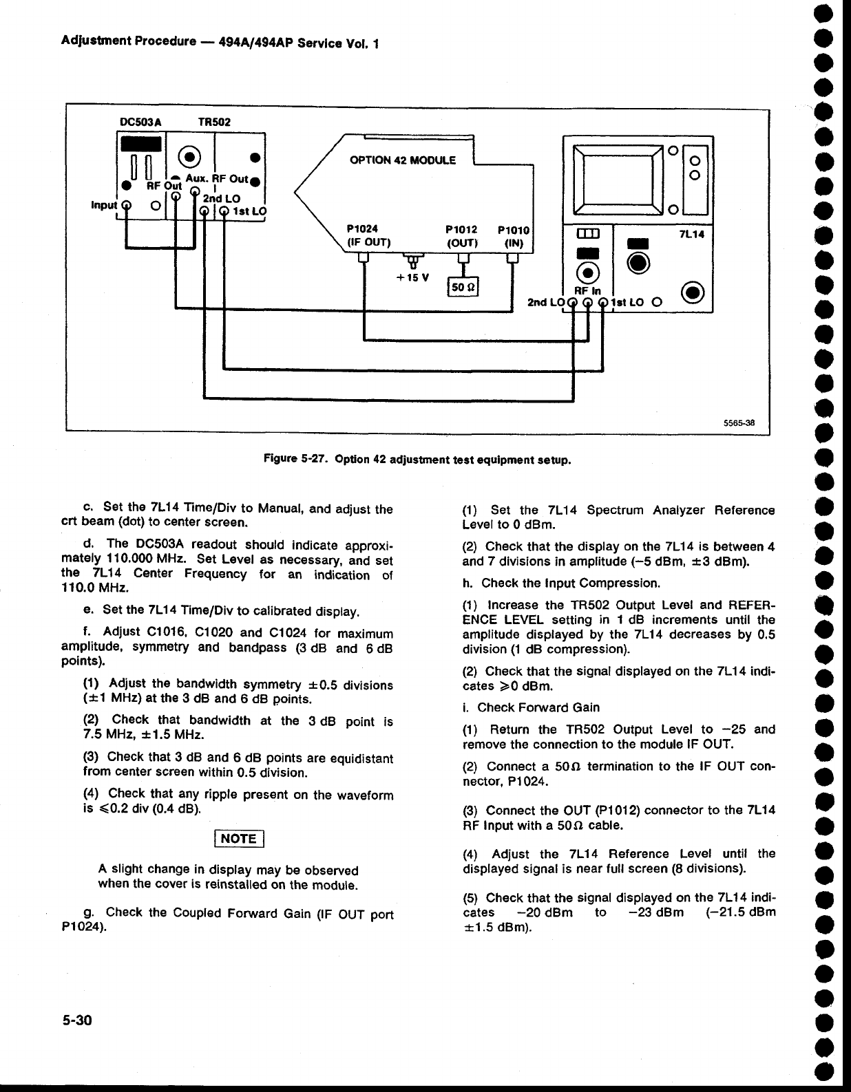
DC503A
I
[[
ORF
oo
lc
ba 1*RF
OurO
LO
lst LO
Input
rrn
I
e
RF ln
I
O
lrtlO O
P1024 P1012 P1010
(rF
ouT) (OUr) (tN) H:N
Adrustment
Procedure
- 4g4A/4g4Ap
Servlce
Vot,
I
o
o
o
o
o
t
I
t
O
t
o
a
t
t
o
a
o
o
o
o
I
t
a
a
I
o
o
o
a
O
a
a
o
a
o
a
o
o
o
o
o
o
o
o
Figure
5-27. Opton 42 adiustment
test equipment setup.
c. set the 7L14 Time/Div
to Manual,
and
adjust
the
crt beam
(dot)
to center
screen.
d. The DC503A
readout
shoutd
indicate
approxi-
mately
110.000MH2.
Set Level
as nec€ssary,
and set
the 7L14 Center Frequency for an indication of
110.0
MHz.
e. set the 7L14
Time/Div
to catibrated
display.
f. Adjust
C1016,
C1020 and C1024
for maximum
amplitude,
symmetry
and bandpass
(3
dB and 6 dB
points).
(1) Adjust
the bandwidth
symmetry +0.5 divisions
(r1 MHz)
at
th€
3 dB and
6 dB points.
(2} Check that bandwidth
at the 3 dB point is
7.5
MHz, *1.5
MHz.
(3) Check
that
3 dB and
6 dB points
are
equidistant
from center
screen
within
0.5
division.
(4) Check
that any
ripple
present
on the waveform
is (0.2 div
(0.4
dB).
A slight change
in display
may
be
observed
when
the cover is reinstalled
on
the
module.
S. Check
the Coupled
Fonuard
Gain
(tF
OUT
port
P1O24l.
(1) Set the 7L14 Spectrum
Analyzer Reference
Level
to 0 dBm.
(2) Check
that the
display
on
the
7L14 is between 4
and 7 divisions in amplitude
(-5 dBm,
i3 dBm).
h. Check the Input Compression.
(1) Increase
the TR502 Output
Level and REFER-
ENCE
LEVEL setting
in 1 dB increments until the
amplitude displayed by the 7L14 decreases by 0.5
division
(1
dB compression).
(2) Check
that the
signal
displayed on the
7L14 indi-
cates
)0 dBm.
i. Check Forward
Gain
(1) Return
the TR502 Output Level to -25 and
remove the
connection to the
modulo ]F OUT.
(2) Connect
a 50o termination to the lF OUT con-
nector, P1024.
(3) Connect
the OUT
(P1012)
connector to the
7L14
RF
Input with a 50o cable.
(4) Adjust the 7L14 Reference
Level until the
displayed
signal is near
full screen
(8
divisions).
(5) Check
that the
signal
displayed
on the
7L14 indi-
cates -20 dBm to -23 dBm (-21.5
dBm
*1.5 dBrn).
5-30
a
o
o
o
a
t
o
o
o
o
I
t
o
I
o
I
a
o
I
t
o
a
o
o
o
O
o
o
a
o
o
O
t
a
o
o
O
O
I
O
o
o
I
I
Sectfon
6 - 494A/494Ap
Servicc
Vot.
1
4. Nothing
capabl€
of generating
or hotding
a static
charge should be allowed on the work station sur-
face.
5.. Keep the cornponent leads shortEd together
whenever
possible.
9 Pick up components
by the body, never
by the
leads.
7. Do
not
slide
the components
over
any
surface.
8. Avoid
handling
components
in areas
that
hav€
a
floor or work-surface
covering
capabfe
of generating
a static
charge.
9. UsE a soldering
iron that ls connected
to €arth
ground.
10. Use only
special
anti-static
suction
type
or wick
type
desoldering
tools.
Voltage
Equlvalent
for Levels:
1-100to500V a-500V
2 - 200to 500
v 5 - 400
to 600
v
3-250V 6-600to800V
a Voltage discharged from a 100 pF capacitor through a resistance
of 100{).
MAINTENANCE
INTRODUCTION
This section
describes procedures
fol reducing
and
pr€venting instrum€nt. malfunction, tioubleshootint
methods, correctave
malntenance,
and procedures
for
recalibrating
those assembties
that normally
do not
require
routine
calibration.
Removing the Instrument trom its Cabinet
T-o
prepare
the standard
instrument
for maintenance
or adiustment,
perform
the
following
steps-
1. S€t
the
instrument
on
lts
facs
or
front
panel.
2. Loosen
the
four
screws
in
th€ feet.
3. Pull
the cover
up and
off.
4. Place
the instrument
on the work bench
and
reconnect
the power cord.
Static-Sensitive Componentg
This
instrument
contains
electrical
components
that
9an be damaged
by static discharge. See
iabte 6_1
for
the relative
susceptibitity
of varioui
classes
of semicon-
ductors. Static
voltages
of 1 kV to 30 kV can occur in
unprotected
environments.
Static
discharge
can damage
any
semicon_
ductor
component
in
this
instrumint.
Observe
the following
precautions
to avoid
damage:
1. Minimize handling of static-sensitive
com-
ponents.
2. Transport
and store
static-sensitive
components
or assembli€s
in their original
containers,
on metal-
ized
or conductive
foam, Label
packages
that
con-
tains static-s
en sitive
as
sE
mbl
ie
s or com,-ponents.
3. Discharge
body static voltage
by wearing a
grounded
wrist strap while handling
these com_
ponents. Statie-sensitive
assemblies or com-
ponents
should be handted
and serviced
only at
static free
work
stations
by qualified
service
person_
nel.
Tabte
6-1
RELATIVE
SUSCEPTIBILITY
TO
STATIC DISCHARGE
DAMAGE
fa400to
1000
V (estl
8-900V
9-1200V
MOS or CMOS microcircuits or
discretes,
or linear
microcircuits
with
TTL
(L€ast
Sensitive)
6-1
PREVENTIVE
MAINTENANCE
Preventive
maintenance
consists of cleaning,
visual
inspection,
performance
check, and if needed
a recali-
bration. The preventive
maintenance
schedule
that is
established
for the instrument
should
be based
on the
environment
in which
the instrument
is operated
and
the
amount
of use. Under av€rage
conditions (laboratory
situation)
a preventive
maintenance
check should
be
performed
every
1000
hours
of instrument
operation.
Elapsed Time Meter
A 5000 hour elapsed time indicator, graduated
in
500 hour increments.
is installed
on
thE Z-AxislRF
Inter-
face circuit board. This provides a convenient
way to
check operating
time. The meter on new instruments
may indicate from 200 to 300 hours elapsed time
because most instruments go through a factory burn-in
tim€
to improve
reliabitity.
This
is simitar
to using aged
components
to improve
reliability
and operating
stabil-
ity.
Cleaning
Clean the instrument
often
enough
to prevent
dust
or dirt from accumulating
in or on it. Accumulation
of
dirt and grease
acts as a thermal insulating
blanket
and
prevents
efficient
heat
dissipation. lt also
provides
high
resistance electrical
leakagg paths between
conductors
or components
in a humid
environment.
Exterlor. Clean
the dust from the outside
of the
Instrument
by wiping or brushing
the surface
with
a soft
cloth or small
brush. The
brush will remove
dust from
around
the front-panel
selector
buttons. Hardened
dirt
may be rernoved with a cloth dampened
in water that
contains a mild d€tergent. Abrasive cleaners should
not be used.
Interlon Clean the interior
by loosening
accumu-
lated dust with a clry soft brush, then remove the
loosened
dirt with low pressure
air to blow the dust
cl€ar. (High velocity air can damage som€ com-
ponents.)
Hardened
dirt or grease may be removed
with a cotton
tipped
applicator
dampened
with a solu-
tion
of mild
detergent
in wat€r. Do not
leave
detergent
on critical memory components. Abrasive cleaners
should not b€ used. lf the circuit board assemblies
need cleaning,
remove
the circuit
board
by referring
to
the instructions
under
Corrective MaintenancE
in this
section.
After cleaning,
allow
the interior
to thoroughly dry
before applying
pow€r
to the instrument.
Maintenance
- 4g4Al4g4Ap
Servlce
Vot.
1
a
o
o
o
o
t
o
t
o
a
I
t
t
o
o
I
o
t
I
o
o
t
a
a
I
o
o
a
a
o
a
o
o
o
o
o
o
o
o
o
o
o
o
o
Do not allow water to get inside any
enclosed assembly or compon€nts such
as
thE hybrid assemblies, RF Attenuator
assembly,
pot€ntiometers,
etc. Instructions
for removing
these
assemblies
are
provided
in the Corrective
Maintenance
part of this
section. Do not clean
any
plastic
materials
with organic
cleaning solvents such as ben-
zene, toluene,
xylene, ac€tone or similar
compounds
because
they may
damage
the
plastic.
Lubrication
Components in this instrument
do not require lubri-
cation.
Fixtures and Tools for Maintenance
Table
6-2 lists kits and fixtures
that are available
to
aid in
servicing
the spectrum
analyzer.
Visual Inspection
After cleaning, carefully
check the instrument for
such defects
as defective
connections
and damaged
parts. The
remedy for most visible
defects
is obvious.
lf heat-damaged
parts
are discovered,
try to determine
the cause
of overheating
before the damaged
part is
replaced;
othenwise,
the
damage
may be
rep€ated.
Transistor and Integrated Circuit Checks
All transistors
and integrated circuits are soldered
on the boards to prevent pin contact problems,
Periodic
checks
of the transistors
and integrated
cir-
cuits is not recommended.
The
best
measure
of perfor-
mance
is the actual operation of the
component in the
circuit. In most
cases any
degradation
in performance
will be detected by the microcomputer
when it runs its
power
up routine. Performance
of these
components is
also checked
during the performance
check or recali-
bration;
any sub-standard transistors
or integrated cir-
cuits will
usually be detected
at that time.
When
handling a static-sensitive,
observe
the neces-
sary
handling
procedures
to prevent
damage.
6-2
o
a
a
o
o
I
o
o
o
a
o
)
t
o
t
o
I
a
t
a
o
e
a
a
t
o
t
o
o
o
t
o
o
o
I
o
I
o
o
o
o
o
I
o
Maintenance
- 494A1494Ap
Service
Vol.
1
Table 6-2
SERVICE KITS AND TOOLS
Nomenclature
Service
Kit consisting
of:
'l Front
panel
extender
1 Power
module
extender
I Accessories
Interface extender
1 Ribbon
cabte
3 Coaxial
cables,
Sealectro
male-to-S€atectro
temate
1 VR
module
handle
1
Circuit
board
extender
assembly
kit
consiiiing
of:
I Left
€xtender
board
2 Right
exlender
boards
1 Right GPIB extender board
1
Frame
eldrusion
for circuit
board extender
6 Screws,
panhead
with
flat and
tockwasheii
screwdriver,
flat,
with
1/4
to 3lg-inch
bit
Screwdriver, posidrive@
440-2
Wrench,
5/1
6-inch
open-end
Hex
drive wrenches,
glg2, SI€/',ZlGzt-inch
Torque
Wrench
Kit
Tekfonix Part No.
006-3286-01
067-0973-00
067-0971-00
067-0972-00
175-2901-00
17$2902-00
367-028s,00
672-0865-01
670-5562-00
670-5s63-00
670-8493-00
426-1527-A0
21 1-01
16-00
003-1324-00
Saving Stored Data in Battery-Backup Memory
lf backup-battery
power to the memory is inter-
rupted,
such as when
changing
the
battery, data
stored
in
battery-backed
up
memory
will
be
lost. This
data can
be down-loaded onto
tape using
the program provided
at the
end of
this section.
Macros cannot be down-loaded onto tape. How-
ever,
these
macros
can
be readily
reconstructed
if they
had
been
saved
on
a tape or disc.
Performance Checks and Recalibration
The instrument performance should be checked
after each 2000
hours of operation
or every
12 months
if the instrument
is used intermittently
to insure max_
imum performance
and assist in lociting defects that
may not be apparent
during regular
operation. Instruc_
tions for conducting
a performance
check
are provided
by the Performance Check section of the service
instructions.
Troubleshooting
Aids
Diagrams - Functional
block and circuit diagrams.
on foldout pages in the Diagrams section, eontain
significant
waveforms, voltages, and togic data informa-
tion. Conditions for getting the data are provided on
the diagram or adjacent to it. Refer
to the Replaceable
Electrical Parts list section for a description of all
assemblies
and components. Diagrams
are arranged
in
signal flow sequence and by sections, such as RF sec-
tion, lF section, frequency control section, etc., with an
accompanying
functional block diagram.
6-3
TROUBLESHOOTING
The spectrum
analyzyer
contains
firmware
that will
troubleshoot the frequency control system and the
power supply. Troublsshooting
procedure
for this sys_
t€m
and
the
power
suppty
is provided
ln
the Diagnostics
part of this section. Also included
with this part is a
description
of the
trace
modes
and
their actions. After
th€
def€ctive
assembly
or component
has
be€n tocated,
refer
to the Replacing
Assemblies
and Sub_assemblies
pert
of this section
tor removal
and
repfacement
instruc_
tions.
Malntenance
- tl94A/494Ap
SeMce Vot. 1
Schematic
diagrams list the Tektronix part No.
(670-xxxx-)
for the assembty
or board atong with the
assembly
number
(e.9.
AS0)
and name. The tast
two
digits or sufftx of the part number
are not indicated
on
the diagram, however,
they are list€d in the El€ctrical
Parts section. These two digits rsflect changes or
modifications to the assembly or board. When a
change
is made to the assembly
the suffx rolls one
digit. The
diagram
indicates
these changes
with
a grey
tint drawing of the original circuit or if a component
changes
value the symbol is enclosed
with a grey tint
box. When
a major
modification
is made
to an assem-
bly or board
and it is no longer
compatible
with
eadier
instruments
a nsw part number
ls asslgned
and a
separate schematic with associated illustrations are
added. all diagrams
indicate
the new part number
and
the instrument
serlal
number
break. lf the assembly
is
compatible
with earlier
lnstruments
and the change
is
significant
enough
to require
a separate
schematic,
this
will
also
be
identified.
Corrections
to the manual
and instrument
modifications
are documented
by ad<ling
conection pages behind a tabbed page,
labeled Change Information,
at the rear of
the manual.
Check
this Change Information
section for changes
to the manual
or thE
instrument.
Circult Board lllustadons and Component
Loeator
Gharts - Electrical
components,
connectors,
and test
points are id€ntifisd on circuit board illustrations
that
are
located
on the insidg
fold of the corresponding
cir-
cuit diagram
or the back of the preceding
diagram. A
grid on the circuit board illustration
and the circuit
sch€rnatic,
plus a look-up
tabl€.
provide
the means
to
quickly
locate
components
on either
the diagram or the
circuit
board.
ln most
cases,
circuit
numbers
are
assigned
accord-
ing to the physical
location
of the component
on the
board
or assembly. The first digit
designates
the row of
a grid, the second the column,
with the last two
reserved
as an expander.
Three
digit numbers
desig-
nate chassis mounted
compon€nts.
Diagnostcs - The spectrum
analyzer contains
firmware
that will assist
in locating
trouble in the fre-
quency control system and the power supply. This
diagnostic
information
is part
of this section.
General Troubleshooting Techniques
Before using test equipment,
to measure
across
static-sensitive
components
or assemblies,
be certain
that voltag€s
or current
supplied
by the
test equipment
does not exceed
th€ limits of the components
to be
tested.
6-4
Try to isolat€ the problem to a component
through
signal analysis. Determine
that circuit voltages
will not
damage
the replacement.
Semlconductor Checks - Semiconductor
failures
account tor the majority of electronic equipment
failures. All semiconductors
are soldered
to the boards
to reduce
pin contact
problems. The following
guide-
lines
should
be observed
if you substitute any
of these
components.
1. Tum the power
off before removing
an assembly
or board.
2. Use a de-soldering tool and 25 W or less solder-
ing iron to remove the components.
3. Use only good components for substitution.
Be
sure
the new component
is inserted
into the board
properly before soldering. Refer to the
manufacturer's
data
sheet for integrated
circuit
and
transistor lead configuration.
lf a substitute is not available,
check
the
transistor
or MOS FET with a dynamic tes-
ter such as the TEKTRONIX Type 576
Curve Tracer. Static type testers, such as
an ohmmeter. can be used to check the
resistance ratio across some semiconduc-
tor junctions
if no other method is available,
however, DO NOT MEASURE RESISTANCE
ACROSS
A MOS FET to avoid damage
from static charges. Use the high resis-
tance ranges (R
x 1k or higher) so the
external
test current is limited
to less than
6 mA. lf uncertain, measure the external
test current with an ammeter. Resistance
ratios across base-to-emitter or base-to-
collector junctions usually run 100:1 or
higher. The ratio is measured by connect-
ing the meter leads across the terminals.
note the reading,
then reverse
the leads
and note
the
second reading.
Dlode Checks - Most diodes
can be checked in
the circuit by taking measurements
across the diode
and comparing these with voltages listed on the
diagram. Forward-to-back resistance
ratios can usually
be taken by referring to the schematic
and pulling
appropriate
transistors
and pin connectors
to remove
low resistance loops around
the
diode.
Do not use an ohmmeter
scale with a high
external
current to check diode
junctions.
Do not check the forward-to-back
resis-
tance
ratios of mixer
diodes.
Diagnostic Firmware
The firmware in the sp€ctrum analyzer provldes
diagnostic
routines
that can be used
wittr
itre Diagnostic
part of this section
to troubl€shoot
th€ Frequency
Con-
trol system
and
diagnose
power
Supply
problems.
This
part fottows GenErat trouOtestrbttini information.
Refer
to this part to help isolate
probljms within
this
!9op. Th9 foilowing
are atso some g€nerat
suggestions
that
may
help
isolate
a problem
when
troubleshooting.
Troubleshooting Steps
1. Ensure
that the problem
exists
in the spectrum
analyzer
by checking
the operation
of associaied
test
equipment.
2. Try to isolate
the problem
to a circuit or at l€ast
board level by evaluating operationaf
symptoms;
for
example,
absence
of the fr€quency
dot coutO
be caused
by a malfunction
in the video summing
stage,
the
marker
generator,
or switching
circuits.
3. Three
levels
of block diagrams
are provided
to
aid in understanding
the
theory
of operation.
The
most
detailed
level
is adiacent
to the schematic
and
usually
provides signal and voltage tevels at critical pointi
within
the circuits. Signal levels
are usually
the
ievels
required
to produce
full screen
deflEction.
4. lnstructions
on how to remov€
or replace
those
assemblies
which
are not obvious,
are provided
in this
section. Refer
to this part before removing
any
assem_
bly for testing
or repairing.
Matntenance
- 494A,1494Ap
Service
Vot.
1
_ _
5. Visually
inspect
the area or assembly
for such
defects as broken or loose connections,
improperty
connected components, overheated or burned com_
ponents,
chafed
insulation,
etc. Repair
or replace
all
obvious defects. In the case of overheated com_
ponents,
try to deterrnine
the cause
of the overheated
condition
and correct
before
applying
power.
6. Use successive
electrical
checks
to try to locate
the problem.
An oscilloscope
is a valuable
t€st item
for
evaluating
circuit
performance.
lf appticable,
check
the
ca-libration
adiustments;
howEver,
before changing
an
adjustment
note its position
so it can be retumed
tb its
original
setting. This will facilitate
recalibration
after
the
trouble
has
been located
and repaired.
7. Dotermine
the extent of the repair needed; if
complex, we recommend contacting your local Tek_
tronix
Field
Office or repres€ntative.
lf minor.
such
as
a
component
replacement,
see
the Replaceable
parts
list
for replacement
information.
Removal
and
replacement
procedure
of the assemblies
and sub-assemblies
are
described
under
Corrective
Maintenanc€.
When
measuring
voltages
and waveforms,
use
extr€me
care
with
the
placement
of test
probes. Because
some
circuit
boards
have
a high component
density, access
to points
in some circuits is limited. A test prob€
could accidentally
short a circuit
and gen-
erate transient voltages that can destroy
many static-sensitive
components.
DIAGNOSTICS
This part consists
of explanations
and procedures
for troubleshooting
the freguency
control
system
and
the
power
supply
using
diagnostic
firmware
in
the spec_
trum analyzer.
TROUBLESHOOTING
USING
THE ERROR
MESSAGE
DISPLAY
Introduction
This
part
contains
procedures
for troubleshooting
the frequency
control
system
and
thE
power
supply.
When
th€ microprocessor
detects a failure
or error
in the Frequency
Control
loops or a failure
in the
power
Supply
voltages
it will cause
the spectrum
analyzer
to
display
an error message
near center
screen
for a few
seconds;
this is followed
by an error status
message
near
th€
top
of the screen
whieh rernains
as long as
the
error
or
problern
exists.
These error messages
pertain to problems
that
exist under current instrument
operational
modes or
front
panel
settings; for example,
an error
that
pertains
to the hardware in the phase
lock loop will exist only
when thE instrument
is in the phase
lock mode
(nar-
rower
span/div settings).
6-5
Malntenance
- 4tt0[l4g4Ap Servlce
Vol. I
Because
the frequency
control
loop may be
unlocked
when using the internal
reference
freguency
in a ucold' instrument.
no error
messag€
is displayed
for the internal
refer-
ence unlocked condition. How€ver, l_U
(lnternat-Untock)
is disptayed
at the
REFER-
ENCE
OSCTLLATOR positaon
for the normal
instrument rEadout. The proc€dure that
deats with FREQUENCY REFERENCE
UNLOCKED
message
shoutd
be foilowed
if
l-U appears
after
the instrument
is warm.
The following
troubleshooting
procedures
are keyed
to the brief
error messages.
Some
problems
may
pro-
duce more
than one error message
in which
caje'the
spectrurn analyzer will <lisplay only th€ predominant
error. A listing
of all error m€ssages
will be displayed
if
you press <Blue-SHIFT>
MAX HOLD. Combinations
of error m€ssages
may
help
determine
and expedite
the
proc€ss
of finding
the problem.
. .
Some of the procedures
use firmware
diagnostics
aid routines
which can only be accessed
by pressing
>Blue-SHIFT> PULSE STRETCHER
anO-
ietecting
menu
item
#3 (DIAGNOST|C
A|DS).
Combination of Error Messages
The following
is a list of error m€ssage
combina-
tions
and
suggestions
as to their cause. lf the
problem
is not resolved
with
the following
suggestions.
or if the
combination
of effor messages displayed is not
covered,
proceed
to the listing
of each
error message
and
how
to troubleshoot
the
problem.
POWER
SUPPLY
OUT
OF REGULATION
(in comblnatlon
wlth any otfrer
meseage/s)
A missing
or inaccurate
supply
voltage
is probably
causing
the other errors. proceed
to the POWER
SUp-
PLY
OUT
OF REGULATTON procedure.
TUNING
FAILURE
- lST LO
and
TUNING
FAILURE
- 2ND
LO
The
CF
Control
board
is probably
the cause,
partic-
ularly if signals
do not tune or do not tune smoothly.
The
problem
is probably
the voltage
reterence
or in the
digital control
section.
Procedure Format
The format
for thes€ procedures
is such that the
problem
is diagnosed
in a dEscending
order. The aim,
to isolate
a problem
down to one part of the system,
usuaily an assembly
(such
as a module
or boardl
or a
functional
section
of the assembly.
After the pr6btem
6-5
1.
has
been isolated
to the
assembly
or circuit
level,
refer
to the diagrams and circuit descr{ption,
as suggested
under General Troubleshooting
Technigues,
for further
isolation.
The procedures
are structured
as follows:
Error Message
Troubleshooting
Procedure
Steps at the same level are either sequential
or
alternative steps, based
on measurement or observa-
tion. Proceed
to the lower-level steps
only
if the
condi-
tions
of the
higher-level
steps are
met. lf the
conditions
are not met,
proceed
to the next step at the same
level.
An "(E)'
at the end of a step,
signifies
this is as far as
this procedur€
can
tak€
you
to locate
the problem.
Several of the troubleshooting
procedures
require
that frequencies
be counted and compared
to either
an
expected
value, or the
number counted
by
the spectrum
analyzer's internal
counter.
The frequencies
can
differ
by up to [(1x10⁷)
+ (counter
accuracy).
These
procedures,
unless
specifted,
assume
the
fre-
quency
range
is either
0
- 1.8
GHz or 1.7
- 5.5 GHz.
Some
failures,
in the
frequency
control
system,
may
appear only at sp€cific oscillator
frequencies. lf this
occurs,
in a higher
frequency range, the fundamental
frequency
of the appropriate oscillator should
be deter-
mined
so it can be set to the same
frequency
in the
lower
bands. This can
be done by:
a.
b.
(1)
(2)
2.
o
o
o
o
o
o
o
o
o
o
o
a
o
o
o
o
o
o
a
o
o
o
o
I
o
o
o
o
o
I
o
o
o
a
o
I
a
o
|
o
o
a
o
o
(1)
Press
<Btue-SHtFT>
PULSE
STRETCHEB
and
#0, then setect
either
the lst to reaoout
lmenu
item #1) or the lnd fg.readout (menu
iteni *e1.
I!9 _LO frequency wiil be displayect
on the crt
CENTER
FREQUENCY
readout
pbsition.
(2[fter n-oting
the.freque^ncy
of the oscillator,
press
<Blue-SHtFT>
PULSE
STRETCHER
and #0, and
select
center
frequency
readout
to return
to the nor-
mal center
frequency
readout
mode.
Since
the
instrument's
power
is usually
switched
on
and off during troubleshooting,
the ponJer-do*n
set-
tings, that are automatically
Ltored in register 0 of
Paltery-backed-up
memory,
lhout6 be recalted
so the
instrument
settlngs
and operating
mode
dupticate
those
that
existed
when
th€ error
message
was
ginerat"d.
. The following,
describes
each error message
and
the
procedures
recommended
to locate
the problem.
POWER
SUPPLY
OUT
OF REGULATION
Any out-of-tolerance
voltage will cause this eror
m.?.":"g.e
to be displayed.
A pow€r
suppty
status
circuit
within
the power
supply
will change
tne itatus LED
on
the
Z-Axis
board
to red,when
any
suppty
except
_17 v
changes
by more
than 25%. An
-error'message
will be
also-
be displayed.
An apparent
power suppty
failure
can
be
produced
when
either
the supply
fails
or a circuit
demands
excessive
current
and Of owi L protective
fuse
or produces
a current limit condition. The following
procedure
should
determine
those voltages
that are out
of range
and whether
the failure
is in th6 supply
or in a
circuit
outside
the
supply.
Troubleshooting procedure
The spectrum analyzer uses a high
eficiency pow€r supply, with the primJry
ground
potential
difierent
from chassis
or
€arth ground. An isolation transformer,
with a turns ratio of 1:1 And a 5OO
VA
minimum
rating,
should be used between
the power source and the spectrum
analyzer power input receptacle, The
transformer
must have
three-wire
input
and
output connectors with a through ground
99!*99n input and output.
- S-tancor
GlS1000 is an €xample of a suitable
transformer.
A iump€r
should
also
be con-
n€cted
between
th€ primary
ground
side
to
chassis
ground
(emitter
of e2061 and the
ground
t€rminat
of the input
fitter
FL301).
Malntenance
_ 4g4Ll4g4Ap
Servlce
Vol. 1
lf the power supply is separat€d
from the
instrument and operated on the bench,
hazardous potentials
exist
within
the supply
for several
seconds
after power is discon_
nected. This is due to the slow
discharge
of capacitors
C6101
and C61fi. DS5112
(next to 96111) tights when the potential
exceeds
80
V.
_ -
1. Verify that the power supply status LED,
on the
Z-Axis board, is red. lf the LED
is green,
there
is prob-
ably
a failure
in the microprocessor
lnterface.
(E)
.2, Measure
the power supply
voltages
at the test
points
on the Z-Axis board. To access
ine test points,
remov€ the hold down cover over the Sweep and
Z-Axis boards.
Hazardous
voltages (900
V and 100
V) are
present
on the Z-axis board.
The ranges
for each
supply
are listed
in Table
6€.
ThEse
are
tolerance
limits
which
are
much
tighter
than
the limits
used by the power
supply
sensing
circuit. A
supply
that exceeds
these limits may not trigger
the
error
message
or cause
the instrument
to malfunction.
The +15
V supply
is adjustable
and affects
the other
supplies.
Refer
to the
Adjustment
procedure
section
of
the
manual
for adjustment
information
if a supply
is
iust
out
of tolerance.
. a. lf all
supplies
are
within
limits
and
the
power
sup_
ply status
LED is r€d, the probtem
is probably
in the
power supply status circuit on the Z-Axis board.
R1065
may
be misadjusted;
adjust
Rl065 to see it the
LED
changes
to green. lf it changes,
set
R1065 at the
center
of
the
'green'range.
(E)
b. lf the
+17 V or -17 V suppty
and
any
other
sup-
ply or supplies
are inaccurate,
or, if both the +9 V and
+5 V supplies
are
inaccurate,
the trouble
is likely
in
the
Power
Supply.
(E)
c. lf the voltage
is high (in absolute
value),
the
trouble
is probably
in
the Power
Supply.
(E)
d. lf the voltage
from a fused
supply
is inaccurate,
the trouble
is probabty
in the power Suppty.
{E)
e. lf the voltage from a fused
supply
is absent,
it
indicates
the fuse could
be blown. To access
the fuses.
remove the cover at the top left hand corner of the
Power Supply module (as viewed from the front of the
instrument),
A blown
fuse generally
indicates
that
one
of the circuits
that this supply
furnishes
is defective;
however,
a fuse
may
open
without an
overcurrent
con-
dition. Replace
the fuse and try again. lf the fuse
opens,
the trouble is definitely in one
of th€
circuits
the
supply
furnishes.
6-7
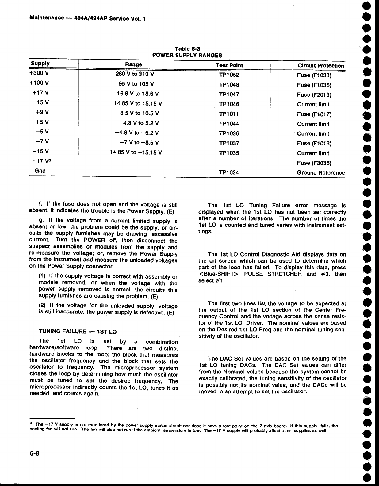
Malntenance
- 494A/494Ap
Servlce
Vol. 1
f. lf the fuse does not open
and the
vottage
is still
absent,
it indicates
the trouble is
the
power
Supply.
(E)
g. lf the voltage
from a current
limited
supply
is
absent
or low,
the problem
could
be the supply,
or cir-
cuits the supply
furnishes
may be drawing excessive
curr€nt. Turn the POWER ofr, then disconnect the
suspect assemblies
or modules
from the supply and
re-measure
the voltage; or, remove
the power Suppty
from
the
instrument
and
measurE
the unloaded
voltagei
on
the Power
Supply
connector.
(1) lf the supply
voltage
is correct
with assembty
or
module removed, or when the voltage with th€
power supply
removed
is normal,
the circuits
this
supply
furnishes
are causing
the
problem.
(E)
(2) lf the voltage
for the unloaded
supply voltage
is still
inaccurate,
the power
supply
is
defective.
(g
TUNING FAILURE
- 1ST
LO
The 1st LO is set by a combination
hardware/software
loop. There are two distinct
hardware
blocks
to the loop:
the block
that measures
the oscillator
frequency
and the block that sets the
oscillator
to frequency. The microprocessor
system
closes
the
loop
by det€rmining
how
much
the oscillator
rnust b€ tuned to set the desired frequency. The
microprocessor
indirectly
counts
the 1st
LO,
tunes
it as
needed, and
counts
again.
The l st LO Tuning Failure error message is
displayed wh€n
the lst LO has not been set correcuy
after a number
of iterations. The number of times the
1st
LO is counted
and
tuned
varies with instrument
set-
tings.
The l st LO Control
Diagnostic Aid displays data
on
the crt screen which can be used to determine which
part
of the loop has
failed. To display this data,
press
<BIUE.SHIFT>
PULSE STRETCHER
and #3. th6n
select
#1.
The first two lines
list the voltage to b€ exp€cted at
the output of the lst LO s€ction of the Center Fre-
quency
Control
and the voltag€
across the sense
resis-
tor of the
l st LO Driver. The nominal values are based
on the
Desired
lst LO Freq and
the
nominal
tuning
sen-
sitivity of the
oscillator.
The DAG
Set
values
are
based
on the setting
of
the
lst LO tuning DACs. The DAC Set values can differ
from the Nominal
values
because the system cannot be
exactly
calibrated,
tbe tuning sensitivity
of the
oscillator
is possibly
not its nominal
value, and the DACS will
be
moved in
an attempt
to set
the
oscillator.
o
a
o
o
o
o
o
o
o
a
o
I
t
o
o
o
o
o
I
I
a
t
o
a
o
a
o
a
o
I
o
o
a
o
a
I
a
o
o
o
o
o
o
a
a The -17 V..:upPty is nol monitored. by trre Power supply status cirouit nor does it have a iest point on the z-axis board, It this suppty rails, the
cooling fan wilt not tun. The fsn will atso not run it tre im5ient tempe.ature is tow. The -17 v suipty witt probably affect other suppliei ai weil.
6-8
Table 6-3
POWER
SUPPLY
RANGES
Supply Range Test Polnt Circult Protecton
+300 v
+100
v
+17
V
15V
+9V
+5V
-5V
-7V
-15
V
-17V8
Gnd
280 V
to 310
V
95Vto105V
10.8
V
to 18.6
V
14.85 V
to 15.15
V
8.5
V
to 10.5
V
4.8
V
to
5.2 V
-4.8 V
to -5.2 V
-7 V to -8.5 V
-14.85
V
to
-15.15
V
TPl052
TPl048
TPl047
TPr046
TPl011
TPl044
TPl036
TPl037
TPt035
TPl034
Fuse (F1033)
Fuse
(F1035)
Fuse
(F2013)
Current limit
Fuse
{F1014
Curent limit
Gurr€nt limit
Fuse (Fl013)
Current limit
Fuse (F3038)
Ground Refer€nce
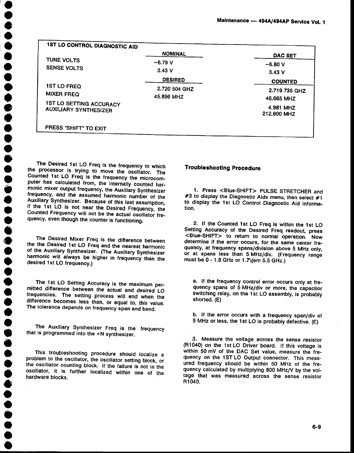
Mafntenance
- 4g4ful4g4Ap
Servtce
Vot.
1
1ST
LO
CONTROL
DIAGNOSTIC
AID NOMINAL
-6.79 V
3.43
V
DESIRED
2.720
504
c|-1.z
45.896
MHZ
DAC
TUNE
VOLTS
SENSE
VOLTS
lST LO FREQ
MIXER
FREO
1ST
LO
SETNNG
ACCURACY
AUXILIARY
SYNTHESIZER
PRESS
'SH|FT"
TO
EXIT
-6.80 V
3.43 V
2.719
735
cHZ
46.665
MHZ
4.981
MHZ
212.800
MHZ
The Desired
l st LO Freq
is th€
frequ€ncy
to which
llre qroge.ssor
,is trying to move the oscillator. The
uounted
l st Lo Freq is the frequency
the microcom-
puter has calculated
from, the internalty
counted
har-
monic
mixer
output
frequency,
the
Auxiliiry
Synthesizer
frequ€ncy,
and the assumed harmonic
numOer
of the
Auxiliary
Synthesizer.
BEcause
of this
lasi assumption,
if the lst LO is not near
the Desired
Frequency,
the
counted
Frequency
wiil not
be the
actuar
osciilator
fre-
quency,
even
though
the
counter
is
functioning.
The Desired
Mixer Freq is the difierence
between
the the Desired
1st LO Fr€q
and
the nearest
harmonic
of the Auxiti.ary
Synthesizer.
(fhe Auxitiary
Synthesizer
laryolig wiil atways
be higher
in frequency
than
rhe
desired
lst LO
frequency.)
The 1st LO Setting
Accuracy
is the maximum
per_
mitted difference.between
the actual
and desired
LO
frequencies.
The setting process
will end when the
difference
becomes
less than,
or equal
to, this value.
The
tolerance
depends
on
frequency
span
and
band.
.. -T" Auxiliary
Synthe.sizer
Freq is the frequency
that
is programrned
into
the
+N synthesizer.
This troubleshooting
procedure
should localize
a
problem
to the oscillator,
the oscillator
setting
block,
or
the.oscillator
counting
block. lf the failur€
is not
in the
oscillator,
it is further localized
within one of the
hardware
blocks.
Troubleshooting procedure
1. Press
<Btue-SHtFT>
PULSE
STRETCHER
and
#3 to display
the Diagnostic
Aids
menu,
then
sefect
#1
to display
the 1st LO Control
Diagnostic
Aid informa-
tion.
2. lf the counted
lst Lo Freq
is within
the 1st Lo
Setting
-Acgyracy
of ths Desired Freq readout, press
<Blue-SHIFT> to retum to normal operation. Now
detennine
if the error occurs, for the same center fre-
quency,
at frequency
spans/division
above
S MHz
only,
or at spans less than 5 MHz/div. (Frequency
range
must
be
0
- 1.8
GHz
or
i.fl(em 5.5
GHz.)
a. lf the frequency
control error occurs
only at fre_
quency
spans
of 5 MHz/div
or more,
the capacitor
switching
relay,
on
the 1st
LO
assembly,
is probably
shorted.
(E)
b. lf the error occurs
with a frequency
span/div
of
5 MHz or less,
the
1st
LO is probably
defective. (E)
3, Measure
the voltage
across
th€ sense
resistor
(R1040)
on the lst LO Driver
board. tf this vottage is
within 50 mV of the DAC Set value,
measure
the fre-
quency
on the l ST LO Output
connector.
This meas-
ured frequency
should be within S0 MHz of the fre-
quency
calculated
by multiptying
800 MHz/V
by the
vot-
tage that was measured
across the sense resistor
R1040.
6-9
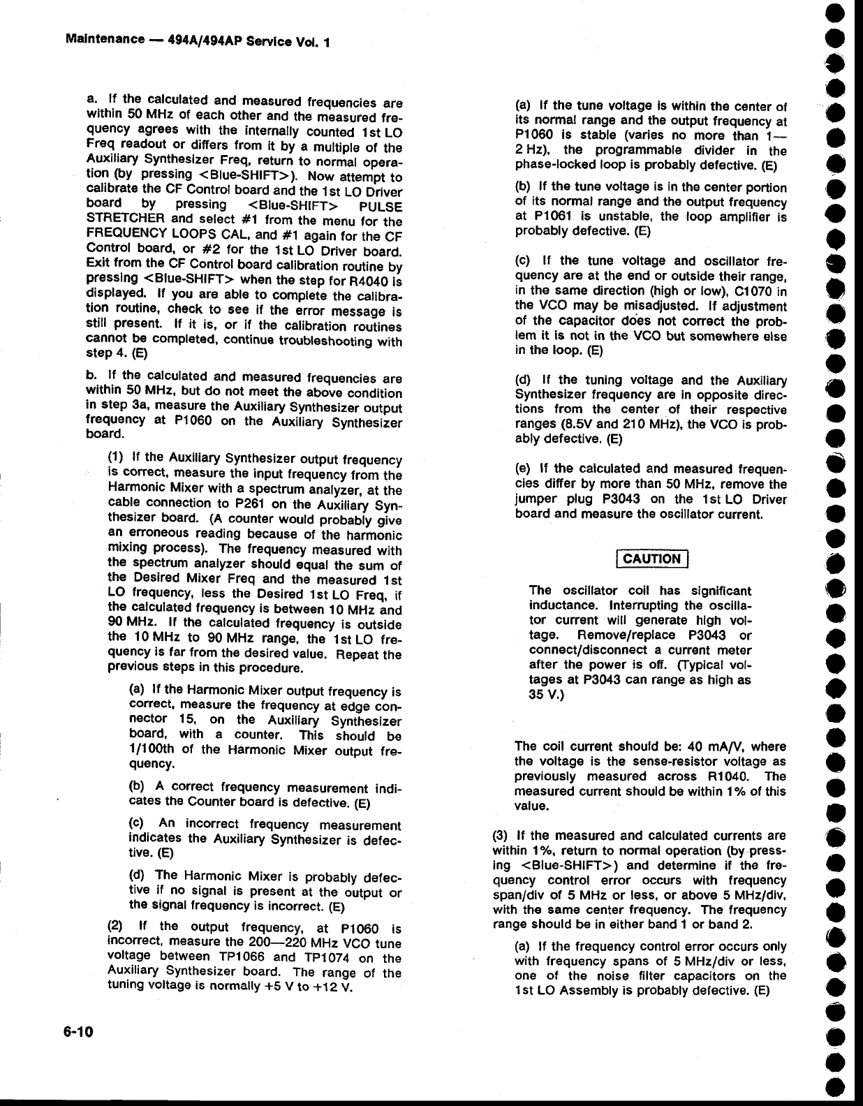
Mafntenance
- 494A1494Ap
Servtce
Vot.
1
a. lf the calculated
and measured
frequencies
are
within
50 MHz
of each
other
and
the
mbasured
fre_
quency agrees
with the internally
count€d
1st
LO
Freg readout
or differs from it by a multiple
of the
Auxiliary
Synthesizer
Freq,
r€turn
to normal
opera_
tion-
(by pressing
<Btue-SHtFT>).
Now
attempt
to
calibrate
the
CF
Control
board
and
the
1st
LO Driver
board by pressing <Btue-SHIFT> PULSE
STRETCHER
and select
#1 from
the menu
for the
FREQUENCY
LOOPS
CAL, and
#1 again
for the
CF
Control board. or #2 for the lst LO Driver board.
Exit from the CF Control
board calibration
routine
by
pressing
<Blue-SHtFT>
when
the step
for Ra040
ii
displayed.
lf you are able
to complete
the calibra-
tion routin€, check to gee if the error message
is
still present. lf it is, or if the calibration
routines
cannot be completed,
continue
troubleshooting
with
step 4. (E)
b. lf the calculat€d
and measured
frequencies
are
within
50 MHz,
but
do not
m€Et
the above
condition
in step
3a, measure
the Auxiliary
Synthesizer
output
frequency
at P1060 on the Auxiliary
Synthesizer
board.
0) lf the Auxitiary
Synthesizer
output
frequency
is coffect,
measure
the input
frequency
lrom the
Harmonic
Mixer
with a spectrum
analyier,
at the
cabte
connection
to p261 on ttre
euiitiary Syn_
thesizer board. (A counter
woutd probaOiy
give
an eroneous reading
because
of the harmonic
mixing
process).
The frequency
measured
with
the speetrum
analyzer
should
equal
the sum of
the Desired
Mixer Freq and the measured
1st
LO frequency,
less the Desired
lst LO Freq, if
the catculated
frequency
is between
10
MHz
and
90 MHz. lf the calculat€d
frequency
is outside
th€ 10
MHz to g0
MHz range,
the lst Lo fre_
quency
is far
from
the d€sired
value.
Repeat
the
previous
steps
in
this
procedure.
(a) lf the Harmonic
Mixer
output
frequency
is
correct.
measure
the frequency
at edge con_
nector 'l5, on the Auxillary synthesizer
board, with a countgr. This should be
1i100th
of the Harmonic
Mixer output fre_
quency.
(b) A correct
frequency
measurement
indi_
cates
the Counter
board
is defective.
(E)
(c) An incorrect frequency measurement
indicates
the Auxiliary
Synthesizer
is defec-
tive.
(E)
(d) The Harmonic
Mixer is probably
defec_
tive if no signal
is present
at the output
or
the signal
frequency
is incorrect.
{E)
(2) tf the output frequency, at p1060 is
incorrect,
measure
fie 200_220 MHz VCo tune
voltage between
Tp1066 and Tp1074 on the
Auxiliary
Synthesizer
board. The range
of the
tuning
voltage
is normally
+S
V to +12 V.
6-10
(a) lf the tune voltage is within
th€ center
of
its normal
range and the output
frequency
at
P1060 is stable (varies
no more than l-
2Hzl, the programmable
divider in the
phase-locked
loop is probably
defective.
(E)
(b) lf the
tune
voltage is
in
th€
center
portion
of its normal
range
and
the output
frequency
at P1061
is unstable, the loop amplifier
ii
probably
defective.
(E)
(c) lf the tune voltage and oscillator fre-
guency
are at the
end or outside
their
range,
in the same
dir€ction
(high
or low),
C1070 tn
the VCO
may
be misadjusted.
lf adjustment
of the capacitor do'es not conect the prob-
lem it is not in the VCO
but somewhere else
in
the loop.
(E)
(d) lf th€ tuning voltage
and the Auxitiary
Synthesizer frequency
are in opposite
direc-
tions from the c€nter of their respective
ranges
(8.5V
and 210
MHz),
the VCO is prob-
ably
defective.
(E)
{e) lf the calculated and
measured
frequen-
cies
difier
by more than
50 MHz, remove
the
jumper plug P3043 on the 1st
LO Driver
board
and
measure the oscillator current.
The oscillator coil has significant
inductance.
Interrupting the oscilla-
tor current will gen€rate
hlgh vol-
tage. Remove/replace
P3043 or
connect/disconnect a current meter
after the power is off. fiypical vol-
tages at P3043
can range
as high as
35
V.)
The coil current should
be: 40 mA/y, where
the voltag€ is the sense-resistor
voltage
as
previously measured across Rl040. The
measured current should
be within 1olo of this
value.
(3) lf the measured
and calculated
currents
are
within 17o. return to normal op€ration
(by press-
ing <Blue-SHIFT>) and determine if the fre-
quency control error occurs with frequency
span/div of 5 MHz or less, or above
5 MHz/div,
with the sam€ center
fr€qu€ncy.
The frequency
range should
be in either band 1 or band
2.
(a) lf the frequency control
error occurs
only
with frequency
spans
of 5 MHz/div or less,
one of the noise filter capacitors
on the
1st
LO Assembly
is probably
defective.
(E)
O
o
o
o
o
I
o
I
o
o
o
o
o
o
o
o
o
o
o
a
a
o
C
o
o
o
o
o
o
o
I
a
t
o
I
o
o
o
o
o
o
o
o
a
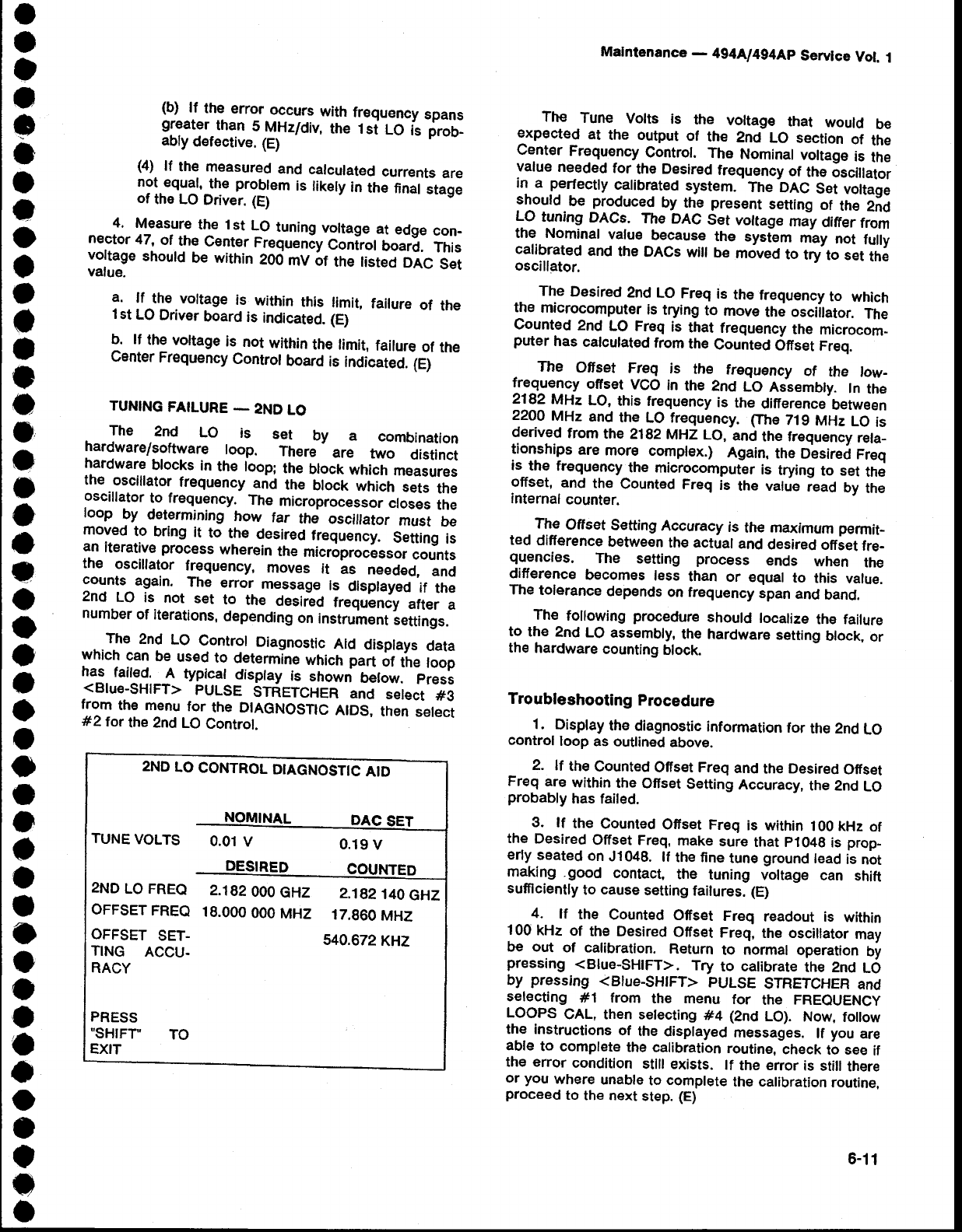
(b) lf the -e1o-r-9cnr: with frequency
spans
greater
than 5 MHz/div,
ttre t si t-O is iroO-
abty
defective.
(E)
(4) lf the measured
and calculated
currents
are
not
equal,
th€ problem
is likely
in the
final
stage
of the LO Driver.
(E)
4. Measure
the lst LO
tuning
voltage
at edge
con-
nector
47, of the Center
Frequeniy
Conirot
boarO.
Ttris
voltage
shoutd
be within
200
mV
6t tne tisteo
DAC
Set
value.
?. lffl".vottage is within
this timit,
faiture
of the
l st LO
Driver
board
is indicated.
(E)
b. tf th€ vottage
is not
within
the
limit,
failure
of the
Center
Frequency
Controt
board
is inOicateO.
6y
TUNING
FATLURE
- zND
LO
The 2nd LO is set by a combination
hardware/software loop. There are two distinct
hardware
blocks
in the loop;
the
block
which
measurEs
the..oscillator
frequency
anO
tne Uoct wfrictr
sets the
oscillator
to frequency.
The micropro""".o, closes
the
roop by d€termining
how far the oscillator
must be
moved
to bring
it to the desired
frequency.
setting
is
an iterative process
wherein
the
microprocesso,
counts
the oscillator
frequency,
moves it as needed,
and
counts
again. The error message
ls displayed
if the
2nd LO is not set to the Oesiid trequlncy after a
number
of iterations,
depending
on
instrument
lettings.
The 2nd LO Controt
Diagnostic
Aid displays
data
which can be used
to deternrine
which part ot t'tre
toop
has.
fait€d._11
typicat
disptay
is snown
below. press
<Blue-SHIFT> PULSE STRETCHER
and setect #3
from the menu
for the DIAGNOSTIC
AIDS,
then
select
#2tor the 2nd
LO
Control.
Malntenance
_ 4g4A/494Ap
Servlce
Vol. 1
The Tune Volts is the voltage that would be
expected at the output of the 2nd Lo section of the
Cent€r
Frequency
Control.
The Nominal
voltage
is the
value
needed
for the
Desired
frequency
of the
6scillator
in a perfecfly
catibrat€d
system.
-me beC Set
vonale
should
be produced
by the present
seuing
of the 2;d
LO tuning DACs. The DAC
Set vottage may ditrer
trom
the Nominal value because_
the system may not fully
calibrated
and
the
DACs
witf
be moved
to tryto set
th;
oscillator.
The
Desired
2nd
LO
Freq
is the
frequency
to which
the microcomputer
is trying
to move
the osciitator.
The
Counted
2nd LO Freq is that frequency
the microcom_
puter has calculated
from
the Counted
Ofset freq.
The Offset Freq is the frequency of the tow-
lr9^e-u9ncy
ofrset VGO
in the 2nd LO Asiembly. ln the
2182 MHz LO, this frequ€ncy
is the difference
between
22OA
MHz and the LO frequency. Ftre 719 MHz LO is
derived
from the Z1g2
MHZ LO,
-ani the frequency
reta-
tionships
are
more complex.) Again,
the
Desired
Freq
is--the
frequ€ncy
the microcomputlr is trying
to set the
offset,
and the Counted
Freq
is the value
iead by the
internal
counter.
.If-|j, Offset€etting Accuracy
is the maximum
permat_
ted difference
between
the actual
and
desired
otriet fre-
quencies. The setting process ends when the
difference
beeomes
less than or equal
to this value.
The
tolerance
depends
on frequency
span
and
band.
The following
procedure
should
localize
the failure
to the 2nd
LO
assembly,
the hardware
setting
block,
or
the
hardware
counting
block.
Troubleshooting Procedure
1. Display
the
diagnostic
information
for the
2nd
LO
control
loop as outlined
above.
2. lf the
Counted
Offset Freq
and
the
Desired
Offset
Freq
are
within
the
Offset
Setting
Accuracy,
the 2nd
LO
probably
has
failed.
3. lf the Counted
Offset Freq is within
100
kHz
of
the Desired
Offset Freq,
make
sure
that
p1049
is prop_
erly
seated
on
J1048.
lf the fine
tune
ground
lead
is not
making .good contact,
the tuning voltage can shift
sufflciently
to cause
setting
failures.
(E)
4. lf the Counted
Offset Freq readout is within
100
kHz of the Desired
Offset
Freq,
the oscillator
may
be out of calibration. Return to normal operation
by
pressing
<Blue-SHIFT>. Try to calibrate
the 2nd LO
by pressing <Blue-SHtFT>
PULSE
STRETCHER
and
selecting #1 from the menu for the FREQUENCY
LOOPS
GAL, then setecting
#4 {2nd
LO). Now,
foilow
the instructions
of the displayed
messages.
lf you
are
able
to complete
the
calibration
routine,
check
to see
if
the error condition
sfllt exists. lf the error
is stiil
there
or you
where
unable
to complete
the calibration
routine.
proceed
to the next
step.
(E)
2ND
LO
CONTROL
DIAGNOSTTC
A'-
TUNE
VOLTS O.O1
V0.19
V
2ND
LO FREQ 2.182
OOO
GHZ
OFFSET
FREQ 18.OOO
OOO
MHZ
OFFSET
SET.
TING ACCU.
RACY
2.182140
c4z
17.860
MHZ
540.672
KHZ
PRESS
"SHIFT'
EXIT TO
6-11
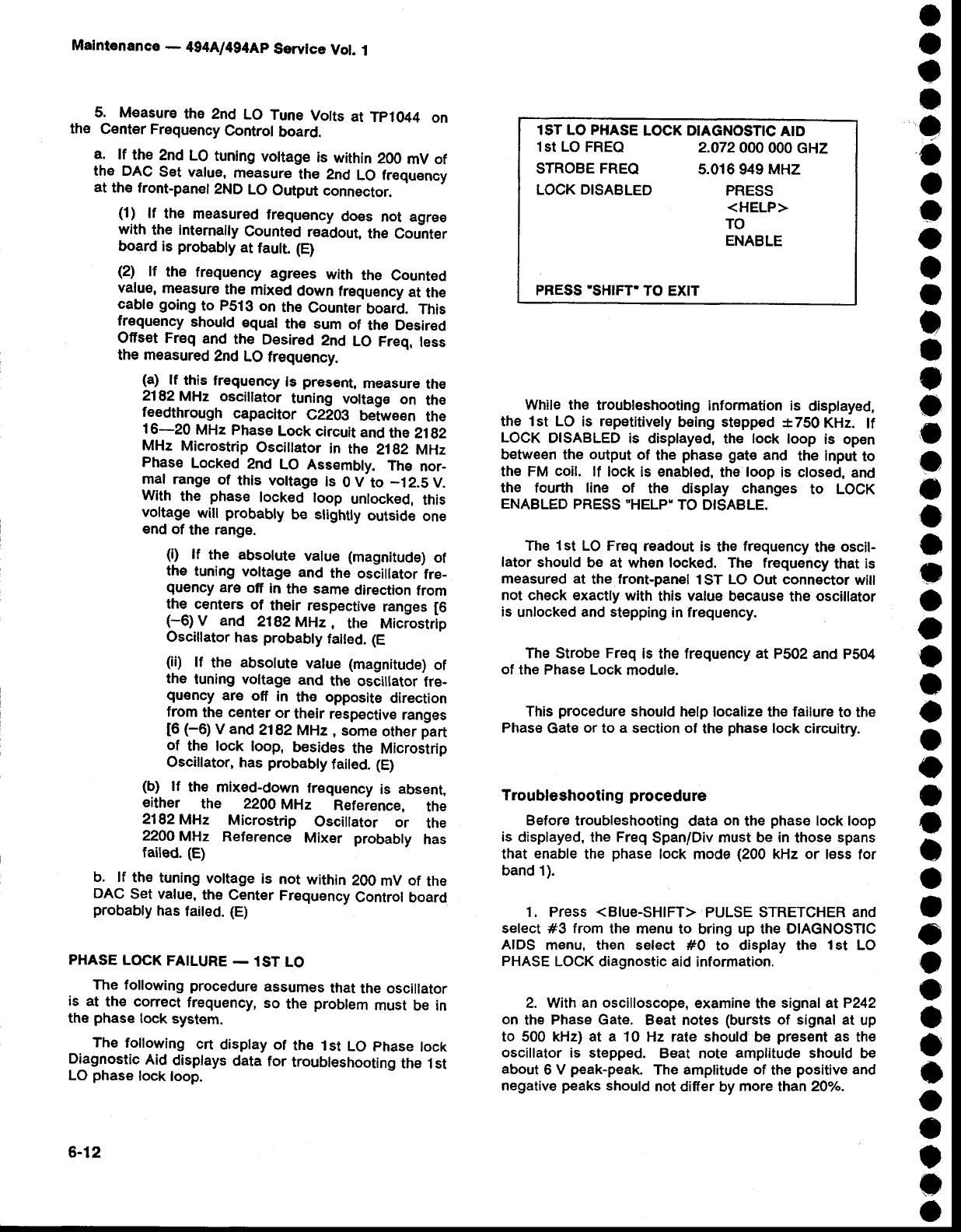
Malntenance
- 494A1494Ap
Servtce
Vol. 1
5. Measure
the 2nd LO Tune Volts at Tp1044 on
the Center Frequency
Control
board.
a. lf the 2nd LO tuning
vottage is within
200 mV of
the DAC
SEt value,
measure
the 2nd
LO frequency
at the front-panet
2ND
LO Output
connector.
(1) lf the measured
frequency
does not agree
with
the internally
counted
roadout.
the couhter
board is probabty
at fautt.
(E)
(2) lf the frequency
agrees with the Counted
value,
measur€
the mixed down frequency
at the
cable
going
to p513
on the Count€r
board. This
frequency
should
equal
the sum of th€ Desir€d
Offset Freq and the Desired
2nd LO Freq,
less
the measured
2nd LO frequency.
(a) lf this freguency
19
present,
measure
the
2182MHz oscillator tuning voltag€ on the
feedthrough capacitor CZaO} between the
16-20 MHz
phase
Lock
circuit
and
the
2tg2
MHz Microstrip
Osciltator
in the 21g2 MHz
Phase
Locked
2nd LO Assemblv.
The nor-
mal
range
of this
voltage
is 0V to -12.5V.
With the phase locked loop unlocked,
this
vottage
wiil probably be stighuy
outside
one
end of the range.
(0 tf the absolute
value (magnitude)
of
the tuning
voltage
and the oscillator
fre_
quency
are ofi in the same
direction
from
the centers of their respective
ranges
[6
{-6) V and 2182
MHz
, the Microstrip
Osciltator
has
probably
faited.
(E
(ii) tf th€ absotute
value (magnitude)
of
the tuning voltage and the oscillator
fre-
quency are off in the opposite direction
from
the center
or their
respective
ranges
16
(-6) V and
2i 82 MHz
, some
other
part
of the lock loop, besides
the Microstrip
Oscillator, has
probably
failed.
(E)
(b) lf the mixed-down
frequency
is absent,
either the 22OO
MHz Reference, the
2182MHz Microstrip Oscillator or the
22AA
MHz Reference Mixer probabty has
faited.
(E)
b. lf the tuning
vottage
is not within
200
mV
of the
DAC
Set
value,
the Center
Frequency
Control
board
probably
has
faited.
(E)
PHASE
LOCK
FAILURE
- 1ST
LO
The following procedure
assumes
that
the oscillator
is at the conect frequency,
so the probtem
must
be in
the phase
lock system.
The following crt display of th€ lst LO phase
lock
Diagnostic
Aid
displays
data
for troubteshooting
th€ 1st
LO
phase
lock
loop.
lST LO PHASE
LOCK DIAGNOSTIC
AID
lst LO FREQ 2.A72000
000 cHZ
STROBE
FREQ 5.016 949 MHZ
LOCK DISABLED PRESS
<HELP>
TO
ENABLE
PRESS'SHIFT'TO
EXIT
While the troubleshooting
information is displayed,
the lst Lo is repetitively
being
stepped
*750KH2. lf
LOCK
DISABLED
is display€d,
the lock loop is open
between the output
of the phase gat€
and the input
to
the FM coil. lf lock is enabled,
the loop is closed,
and
the fourth line of thE display changes to LocK
ENABLED
PRESS
"HELP"
TO
DISABLE.
The lst LO Freq
readout
is the
frequency
the
oscil-
lator should be at when locked. The frequency
that is
measured at the front-panel
1ST LO Out connector
will
not
check exactly with
this value
because
the
oscillator
is unlocked
and
stepping in frequency.
The Strobe
Freq
is the frequency
at P502 and
P504
of the Phase Lock
module.
This
procedure
should
help
localize the failure
to the
Phase
Gate
or
to a section of the
phase
lock
circuitry.
Troubleshooting procedure
Before troubleshooting
data
on
the
phase
lock loop
is displayed,
the
Freq
Span/Div
must be in those
spans
that enable
the phase
lock mode
(200
kHz or l€ss for
band 1).
1. Press
<BIue-SHIFT>
PULSE
STRETCHER
and
select #3 from
the menu to bring
up the
DlAGNosTlc
AIDS menu, then select #0 to display the 1st LO
PHASE
LOCK diagnostic aid
information.
2. With an
oscilloscope,
examine the
signal atP242
on the
Phase Gate. Beat notes
(bursts
of signal at up
to 500 kHz)
at a 10 Hz rate should'be
present
as th€
oscillator
is stepped. Beat note amplitude
should be
about
6 V peak-peak.
The
amplitude of the
positive
and
negative
peaks
should
not
differ by
more
than
2Oh.
6-12
a
o
I
o
)
o
t
o
o
I
o
)
a
o
o
|,
a
o
t
o
a
o
o
I
t
o
I
o
o
o
a
a
I
o
o
O
o
e
o
o
a
o
e
I
a. lf.b€at
notes
are present,
press
HELP
to enable
the lock. Check the- Error' Amplifiei output at
T?2O3T,
on th€ Error
Amplifier
OolrJln the prrase
Lock module. gutput signat
amptituOe'sfroufO
Oe
approximately 6 V peak-peak aho its frequency
should
be 10 Hz. fhe up anO
Oown-oui.t_r"ng"
:igngj:, on edge connectors
g and 10 oi tn" error.
Amplifier
board,
shoutd
be toggling
Oetween
0 V and
+5 V.
(1)..1f
there
is a signat
at Tp2O37
but
one
or both
or tne out-of-range
lines
is not
toggling,
the out-
of-range comparator on the frior- Amptifier
board, or the sensing
circuit on the phase Lock
Controt board, has probabty
failed. firis coutO
cause problems
in maintaining
lock but not in
acquiring lock. lf the instrument does not
acquire
lock. note the out-of_range
problem
and
continue
troubteshooting
with steF
gj.
(2) lf there is no signal at Tp20g7, the Error
Amplifier
has probabty
failed.
(E)
(3) ff there
is a signal
atTp2A}Z,
th€ switching
circuit that connects the output of the Error
Amplifier
to th€ FM coil of tne
i st LO has
prob_
ably
failed.
(E)
P lf b€at
notes
arg present,
but their
amplitude
is
::::_^T"l !:9 v (peak-peak),
or the amptitude
qrnerence
of the
positive
and
negative
sxcursions
is
more than 2AVo,
the phase GatJ is probably
defec-
tive. (E)
c. lf there are no beat notes, mEasure
the strobe
frequency,
at p504
on the phase
l_ocf
moOuie.
(1) lf the strobe
frequency
is the same
as the
readout
on
the
diagnostic
aiO
display,
it is possi_
ble,
but not probable,
that
the r it [o system
is
miscalibrated
and that th€ lst LO is near
tne
wrong harmonic
of the Auxiliary Synthesizer.
Press
<Blue-SHIFT>
to return
to'normat
opera-
tion and
look
at the calibrator
line
that
is
ctosest
in. frequency
to the frequency
(in Band 1) at
which the error occurs. lf the irequency
indi_
cated
for the
calibrator
line
is correci
(a
multiple
9t..
tlO MHz), the phase cate has proOa-Uty
failed.
lf the frequency
indicated
is incorrect,
attempt
to
calibrate
the 1st LO system
by pressing
<Blue-
SHIFT> PULSE
STRETCHER-
and sete-cting
#1
(FREQUENCY
LOOPS CAL), and tben #O
(OVERALL
SYSTEM)
from the rnenu. Exit from
the calibration
routine when the display for
R4040, on the CF.
_C*ontrol
board appears by
pressing
<Blue-SHIFT>. lf the calibration
can
not b€ completed,
or it does not rEsult
in the
correct frequency
indication
for the calibrator
rine,
troubleshoot
the lst LO system
using
the
procedure
under TUNTNG
FAIiURE _rst LO
error
message
step
3b.
(E)
Malntenance
- 4g4Ll4g4Ap
Service
Vol.
1
(2) lf there
is no strobe
signal,
check
for a sig-
nal on feedthrough
M, on the Strobe Driver
board
in
the Phase
Lock
module.
(a) lf there
is a signat,
the
Strobe
Driver
has
probably
faited.
(E)
(b) lf there is no signat,
the
Controiled
Oscit-
lator
has
probably
faited. (E)
(3) lf the frequency
of the strobe signal is
effoneous.
but is stable (within
1_2 Hz), in the
normal strobe range of 5.006477
MHz to
5.018868
MHz,
the programmabte
divider
in the
Synthesizer
has
probabty
faited. (E)
(4) lf the listed
Strobe
Freq
is betow
5.OOZ10O
MHz and
the actual
strobe
frequency
is slightly
above
th€
desired
frequency;
orabove
5.01g240
MHz and
the actual
strobe
frequency
is slightly
below the desired frequency,
attempt
to cali_
brate the Phase Lock Synthesizer. press
<BIue-SHIFT>
PULSE
STRETCHER
and
select
#1, then #5. lf you are able
to complete
the
calibration,
check
to see
if the error
message
is
still
present.
lf it is stilt
displayed,
or
the
calibra_
tion routine
could
not be completed,
proceed
to
th€ next step as if th€ strobe
frequency
was not
within
the above
range. (E)
(5) lf the listed
Strobe
Freq
is outside
the
range
in th.e
pr_ejgding
step, measure
the tune voltage
for the VCO,
at feedthrough
H on the Controll€d
Oscillator
board
in the
phase
Lock
module.
The
normal
range
is from 5.9 V to 11.3
V. With
the
loop unlocked,
the voltage
wiil probably
be near
or beyond
one end of the range.
(a) lf the voltage
is around
the
center
of the
range,
the loop filter and amplifier,
on the
Error
Amplifier
board,
are probably
at fault.
(E)
(b) lf the tuning vottage
and
the strobe
fre-
quency
are
displaced
from
the
center
of their
range (8.6
V and 5.013
MHz) in the same
direction,
the VCO is good and something
else
within
the loop
has faited.
(E)
(c) lf the tuning voltage
and
the strobe
fr€-
quency
are displaced
in opposite
directions
from
the center
of their range,
th€
VCO
has
probably
faited. (E)
6-13
Malntenance
- 4S4Al4g4Ap
Servtce
Vol.
1o
a
o
o
a
a
I
o
o
t
o
t
a
o
o
o
t
o
t
o
o
o
o
a
o
a
t
o
o
o
a
a
a
o
o
o
o
I
t
o
o
I
o
a
TRACE
MODES
Trace Mode provides information
on how the fre-
quency control system is working. lt is acc€ssed by
pressing <Blue-SHtFT> PULSE
STRETCHER.
menu
item
#7, then selecting
lst LO (menu
item
#1),2nd LO
(menu
item
#2} MARKER
(menu
item
#3),
or CORREG_
TION TIMER
(menu
item #4), gRD tF dOUrur (menu
item
#5),
or DISPLAY
RESULTS
(menu
item
#6).
Trace Mode 1, starts tracing the l st LO control
actions. Trace Mode 2, starts tracing
the 2nd LO con_
trol actions. Trace Mode g, starts
tracing
signal
counts.
Trace
Mode
4 starts
tracing marker
conection
cycles.
Information
from these
four trace modes
is stored in
RAM and can be disptayed by setecting
DtSpLAy
RESULTS
(menu
item
6) from
the
TRACE
MbDE menu.
This mode
disptays
up to 16 lines
of data
gathered
by
the trace modes.
Information
used
is obtained
only
wh€n
the
internal
frequency
correction
occurs.
Thihs correction is related to the drift rate
of the spectrum analyzer. The time
between corrections can be as long as
30
s.
To assure
information
is available,
change
th€ FREO SpAN/Dtv one position then
retum. This forces the correction
cycle to
occur.
For modes
1 and
2, the flrst field
of the
display indi-
cates which mode was active at the time the informa-
tion was
gathered.
The second
field
of th€
display
indi-
cates which attempt at tuning or correcting
the oscilla_
tor the data is for. The next lield contains
the tuning
DAG settings before a tune or conection took ptace.
The first three digits are the upper DAG settings, the
next
three dagits
the
lowEr
DAC
s€ttings.
The
next
field
contains
the DAc settings
after
the
tuning
or correction
was attempt€d. Again, the first three digits are the
upper DAC,
and the next three digits
the lower DAC
settings. The next field indicates the time delay
between setting
the DACS
to the new
values
and read-
ing
the resulting
frequency,
in units
of millisecond.
The
final field contains
the frequency
of th€ oscillator
in
question,
after
the tune or correction
attempt.
Actually,
the displayed frequency
is the beat
note
frequency
from
the auxiliary
mixer for the l st LO (in KHz), and the
16-20 MHz oscillator
frequency
for
the
2nd
LO.
For mode
3, the resulting
trace
display
consists
of
seven columns.
The
first column
is always
g. indicating
that the marker
is being traced. The second
column
gives
the iteration
number
of the
correction
cycle
which
the displayed line
describes.
The
third column
consists
of two lefters
and a number. The first
letter is p if the
6-14
data applies to the primary marker and S if the data
applies
to the secondary
marker. The second letter is
c if th€ oscillators are being counted at the marker
position
to determine
the marker
frequency,
or S if the
marker
position
is being synthesized
to maintain
a con-
stant
marker
frequency.
The
number
in this
column
is 1
if the 1st LO
is being counted at the
marker
and
2 if the
second
LO is being counted.
The fourth column
is the
hexadecimal setting of the marker DAC. The fifth
column
is the decimal digital storage
location
of the
mark€r.
The
sixth column
is the
oscillator
settling
time
in ms before
the count. The last column is the har-
monic mixer output frequency
in KHz for a 1st LO
count,
or the
16-20 MHz
VCO fr€quency
for a 2nd
LO
count
at the rnarker
position.
The
sequencE <Blue-SHIFT>
PULSE
STRETCHER,
#7, #0, terminates
trace
actions
and erases
the RAM
of alldata.
Alternate Frequency Display
The Alternate
Frequency
Display mode selects
an
alternate
frequency display instEad
of the
normal
Genter
Frequency
display. These alternate
frequencies
are
selected by pressing <Blue-SHtFT> PULSE
STRETCHER, selecling
menu item #0, and selecting
#0, #1, or #2 as indicat€d
by the
menu.
The normal
Center
Frequency
is displayed when
#0
is selected.
The
frequency
of the
1st
LO is
displayed
when
#1 is
selected.
This display is updat€d
each
time ths 1st
LO
frequency
is counted.
The frequency of the 2nd
LO is displayed
when
#2
is selected.
This display
is updated each
time the tre-
quency
of the
2nd
Lo is counted.
Auxiliary Synthesizer Control
The Auxiliary
Synthesizer Control can be turned
on
continuously, or turned
on only
during
correction
for
the
1st LO
tunes. This mode is toggled
(turned
on continu-
ously or during 1st LO corrections)
by pressing
<Blue-
SHIFT> PULSE
STRETCHER,
and selecting menu item
#4, A message will come
on screen indicating which
mode
the
Auxiliary
Synthesizer
is in.
Correction Disable/Enable
Correction
of the 1st and 2nd LO frequencies can
be disabled
or enabled
by pressing
<Blue-SHIFT>
10
dB/DlV or <Blue-SHIFT> PULSE
STRETCHER,
and
selecting
menu item #6. When corrections
are dis-
abled.
the oscillator frequencies
are counted but no
further
action is taken. This mode
can
be used
to moni-
tor the drift of the oscillators
by activating
the respec-
tive trace mode. When corrections are disabled.
the
1st
LO
cannot
be phase
locked!
CORRECTIVE
MAINTENANCE
o
o
o
o
o
o
I
o
o
o
)
)
I
t
o
t
I
o
C
o
t
o
o
o
t
o
o
o
o
o
o
o
t
o
a
o
o
C
o
o
J
o
I
o
Maintenance
- 494Al4g4fup
Service
Vof.
1
Corrective maintenance
consists of component
replacement
and instrument
repair. Speciat
tecnhiques
and procedures that may be iequirJj to-remove and
replace
assomblies
and/br "ompon"nis
in tnis instru-
msnt
are
described
here.
Handling Static Sensitive Components
Most semiconductor..types,
both separatety
and in
assembliEs,
are
susceptible
to damage
to statii charge,
see
Table
6-1
for voltage
levels.
WJrecommend
static
sensitive procedures
be implemented
for att
operations
involving
semiconductor
handling.
Obtalning Replacement parts
All electrical
and mechanical
parts are available
through your locat
Tektronix
Field
dffic; oi'r"pr"r"nt"-
tive. The Replaceabte
parts
rist
section
contains
infor-
mation
on how
to order
these
replacement
parts.
Some
components
that are heat sinked
to
the circuit board
extrusion
or module
wall,
are soldered
to the board
after the board
is
mounted in place. This is necessary to
avoid
cracking
the case
when
the
mounting
lgrew ls tightened. These
components
are
identified
by a note
on the
schematic
draw-
ilg. .Their part number appears with
chassis mounted componenis in the
Replaceable
Electrical
parts
list.
Parts orientation
and lead dress should
be dupli_
cated because some components are oriented to
reduce interaction between circuits or control circuit
characteristics.
Where
applicable,
an improved
part will b€ substi_
tuted.when
a replacement
is ordered. tf the change
is
complex, your local Field Office or representative
will
contact you concerning
the change. After repair,
the
circuits
may
need
recalibration.
Parts Repair and Return program
Assemblies
containing
hybrid
circuits
or substrates
in a semi-sealed
module,
and
complex
assemblies
such
as
ths 1st
LO,
829
MHz
conv€rter,
or phase
gate
ctetec-
tor, can be returned
to Tektronix
for repair
under
the
repair
and
return
program.
Tel(ronix iepair centers provide
,replacement
or
repair
service
on maior
assemblies
as well
as the
unit.
Return
the instrument
or assembly
to your local
Field
Office
for this seMce, or contact
your
l6cat
Field
Oftce
for repair
and exchange
rates.
Firmware Version and Error Message Readout
This feature provides readout of the firmware
ver_
sion
when
the power
on/off
is cycled. During
the initial
power-up
cycle,
the instrument
firmware
and
iront panel
firmwar€
versions
are displayed
on the crt for approxi_
mately
two seconds.
The Replaceabte
Electrical
parts
list section,
under
Memory
board
(A54),
lists
the ROM
devices and their Tektronix part' numbers
for each
firmware
version.
Whenever
an error occurs in an operational
routine,
an eror message
on screen describes
the nature of
the error. Status messages
or prompts
(see
Diagnosi-
tics part of this section),
are also displayed
when run-
ning
a diagnostic
test
or calibration proceiure.
Selected Components
A few components
that are selected
to meet
certain
parameters
such as temperature
compensation,
or to
center the range of some adjustable
component. The
selected components
are identified
as selectable
on
the circuit diagram
and in the Replaceable
Electrical
Parts
list. The
Replaceable
parts
list
description
for
the
component
gives
either
a nominal
vatue.
The
procedure
for selection
is explained
in the adjustment part of
recalibration procedure. Table 6-4 lists these com-
ponents,
their nominal
values, and
the criteria
for selec_
tion.
Replacing EPROM
or ROM Devtces
Firmware
for the microcomputer
is contained
in
ROM
packs
on
the Memory
and
GplB
boards.
Refer
to
the
Replaceable
Electrical
parts
list (vot.
2)
under these
assemblies
(A54
Memory
and A56 GplB) for the ver-
sions and integrated circuit part numbers. All
integrat€d
circuits are soldered
into sockets on the
board
to reduce
problems
that occur
due
to poor
con-
tact becaus€
of corrosion or loose pins. Refer to
replacing
Transistor
and Integrated
Circuit for pro-
cedure.
6-1s

Malntenance
- 494A1494Ap
Service
Vot.
1o
o
o
o
o
o
)
o
o
o
o
I
o
t
I
a
a
o
o
o
f
o
a
a
t
o
o
o
)
o
I
o
a
o
o
o
o
I
o
o
t
a
t
o
Table 6-4
SELECTED
COMPONENTS
t Number
422A1Rl070
422A1R2049
422A1R2070
422A1R2072
A46A1R1011
1Rl012
446A1Rl013
446A1 Rl014
A46A1
Rl015
446A1Rl010
1R1020
446A1Rl048
Rl049
446A1R1050
1Rl
A46A1Rl052
A46A1Rl053
A46A1Rl055
45045C1038
450A5C1048
450A2C1016
A50A2C1018
A50A2C1032
450A2C1024
Surface-Mounted Components
Surface-mounted
components are used in this
instrument. These
components
are mounted
on pads
on the circuit
board,
rather
than through
holes
in the
board. (ln some rare instances,
components
may be
mount€d on pads around through holes.) Lead
configurations
of
these
components
are
shown
in Figure
6-1.
The positive end of electrolytic capacitors is
identified
with a band. Other
capacitors
and resistors
have no
visible identification.
However, like
their
axial-
leaded
counterparts,
their
values
can
be measured
with
a meter.
Surface-mounted
semiconductor
devices
are sensi-
tive to static €lectricity
discharges,
and should be
treated as
outlined in
the
beginning of this section.
Selection Crlteria
Sets Reference Mixer
output
at 18
MHz
linearity of the 2nd
LO
sweep
Adjusts 2nd LO
tune range
Sets
2nd LO
sweep
Matched
for
temperature coefficient
to 5PPM/oC
Matched for temperature coefficient
to SPPM/"C
Match€d for t€mperature coefficient
to SPPM/oC
Matched for temperature coefiicient to SPPMI"C
Matched
for temperature coefiicient
to SPPM/"C
Matched
for
temperature
coefficient
to SPPM/oC
Move
C1041
frequency
adjustment range
Move
Cl042 frequency
adjustment range
FL1
024 inputloutput i mpedance match
3.3 pF-27 pF
3.3
pF-27 pF
3.3 pF-27 pF
.#
TRATT|3IION
#.
OIO€
E CATE
I
2
t
a
t
f
c
5
t- \
c
6-16
Figure
6-1. Surface-mounted
components
lead conliguration.
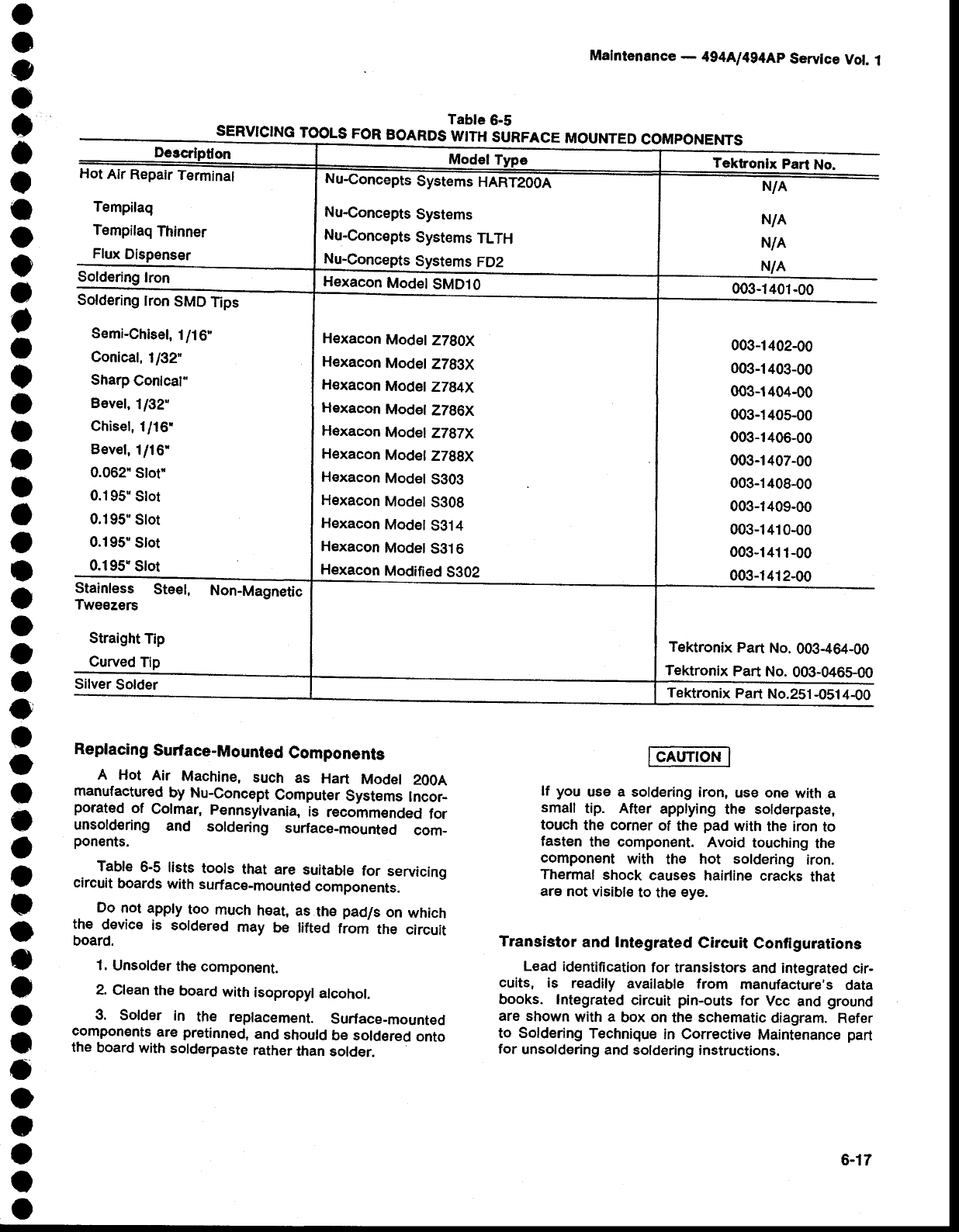
o
o
3
o
o
o
o
o
o
o
o
)
I
I
o
I
a
I
o
o
I
o
o
o
o
o
o
o
o
o
a
o
o
o
o
o
o
t
o
o
a
a
o
o
Mafntenance
- 494[l4g4Ap Servtce
Vot.
1
SERvIcING
TooLs
FoR
BoARD'Tffi3.i*,o"=
MouNTED
coMPoNENTs
Replacing Surface-Mounted Components
A Hot Air Machine,
such as Hart Model 200A
manufactured
by Nu-Concept
Computer
Systems
lncor_
porated
of Colmar,
pennsylvania,
is recommended
for
unsoldering and soldering surface-mounted
com-
ponents.
Table
6-5 lists tools that are suitable
for servicing
circuit
boards
with
surfac€-mouni€d
components.
. Do not apply
too much heat,
as th€ pad/s on which
the device
is soldered
may be lifted
fiom the circuit
board.
1.
Unsolder
the
component.
2.
Clean
the
board
with
isopropyl
alcohot.
3. Solder in the replacement. Surface-mountecl
components
are
pretinned,
and
shoutd
be soldered
onto
the
board
with
solderpaste
rather
than
solder.
lf you use a soldering
iron,
use one
with
a
small tip. After applying
th€ sotderpaste,
touch the corner
of the pad with the iron to
fasten
the component.
Avoid
touching
the
component with the hot soldering iron.
Thermal
shock
causes
hairline
cracks
that
are
not visible
to the
eye.
Transistor and Integrated Circuit Confi
gurations
Lead identification
for transistors and integrated
cir-
cuits, is readily available
from manufacture's
data
books. Integrat€d
circuit
pin-outs
for Vcc and
ground
are shown
with a box
on
the
schematic
diagram. Refer
to Soldering
Technique
in Corrective
Maintenance
part
for unsoldering
and
soldering instructions.
Model Type Tektronix Part
No.
Hor
Alr
Hepair
Terminal
Tempilaq
Tempilaq
Thinner
Flux
Dispenser
Soldering
lron
Nu-Concepts
Systems
HART2OOA
Nu-Concepts
Systems
Nu-Concepts
Systems
TLTH
Nu-Concepts
systems
FD2
N/A
N/A
N/A
N/A
Hexacon
Model
SMD1O 003-1401-00
uordertng
tron
SMD
Tips
Semi-Chisel,
1/16'
Conical,
1132'
Sharp
Contcat"
Bevel,
1/32"
Chisel,
1/16'
Bevel,
l/16'
0.062"
Stot"
0.195"
Slot
0.195"
Slot
0.195'Slot
0.195"
Stot
Hexacon
Modet
ZTAOX
Hexacon
Modet
ZTB}X
Hsxacon
Modet
ZI&4X
Hexacon
Model ZZ$6X
H€xacon
Model
ZZ|TX
Hexacon
Modet
ZT$BX
Hexacon
Model
5303
Hexacon
Model
S30g
Hexacon
Model
S314
Hexacon
Model
3316
Hexacon
Modified
3302
003-1402{0
003-1403-00
@3-1404-00
003-1405-00
003-140&00
003-1407-00
003-1408-00
003-1409-00
003-1410-00
003-141
1-00
003-1412-00
titainbss Steel, Non-Magnetic
Tweezers
Straight
Tip
Curved
Tip Tektronix
Part No.
003464-00
Tektronix
Part No.
003-046$.00
Tektronix
Part
No.251
-051
4-00
6-17
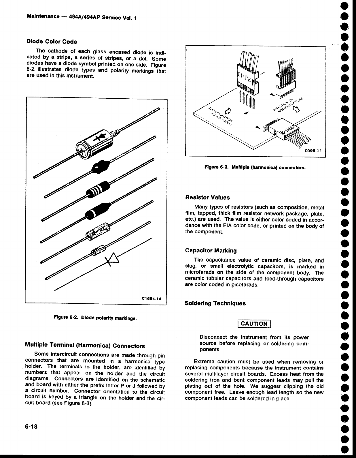
ct66.t-14
Figure
6-2. Diode polartty marklngs.
Maintenance
- 494A/494Ap
Servtce
Vot.
1
Diode
Color
Code
The cathode
of each glass encased
diode
is indi-
gated
by a stripe,
a series
of stripes,
or a dot. Some
diodes
have
a diode symbol
printed
on
one
side. Figure
6-2 illustrates
diode types Lnd potarity
markings'that
are
used
in
this
instrument.
Multiple Terminal (Harmonica) Connectors
Som€ int€rcircuit
connections
are made
through
pin
connectors that are mounted in a harmonica-
type
holder. The terminals
in the holder,
are identified
ty
numbers that appear on the holder and the circuit
diagrams. Connectors
are identified
on the schematic
and
board
with
either
the prefix
letter
p or
J followed
by
a circuit number. Connector
orientation
to the circuit
board
ls keyed
by a triangle
on the holder
and
the cir_
cuit
board
(see
Figure
6-3).
6-18
Flgure
6-3. Multpln (harmonlca)
conneciors.
Resistor Values
Many
types
of resistors (such
as composition,
metal
film,
tapped,
thick film resistor
network
package,
plate,
etc.) are used. The value
is either
color coded
in accor-
dance with the EIA color code,
or printed
on the body
of
the
component.
Capacitor Marking
The capacitance
value
of ceramic
disc, plate,
and
slug, or small electrolytic
capacitors,
is marked in
microfarads
on the side of the component
body. The
ceramic
tubular capacitors
and
feed-through
capacitors
are
color coded
in picofarads.
Soldering Techniques
Disconnect
the instrument
from its power
source
before
replacing
or soldering com-
ponents.
Extreme
caution must be used when removing or
replacing
components
because
the instrument
contains
several multilayer
circuit
boards. Excess heat from
the
soldering iron and bent
component
leads may pull
the
plating
out of the hole. We suggest clipping
the old
component
free. Leave
enough
lead length so the
new
component leads
can
be soldered
in place.
o
o
o
o
a
o
o
o
o
o
I
o
I
t
o
o
o
o
I
o
o
o
a
a
I
o
a
o
)
a
a
o
o
o
o
I
o
o
o
o
c
a
o
o
ffi.
-
\
(x)95-11

o
a
a
o
o
o
o
o
o
o
o
a
o
o
o
t
O
I
o
o
e
a
o
o
o
c
o
o
I
o
o
a
o
o
a
o
a
o
o
O
o
O
o
o
lf you desire
to remove
the component
l€ads,
use a
J.5 Y ol tess
pencil
type iron. Straigtrten-the
teads
on
me oacK
side
of the board;
then
when
the
sotder
melts,
gently puil the sotdered tead through the hote. A
desoldering
tool should be used to
-remove
the old
solder. Use
a desoldering
toot
that
has
a low build-up
of static
charge,
such
as SiMerstat
Soldapullt
desolder-
ing
tool,
when
unsoldering
integrated
circuiis
or transis_
tors.
Replacing the Square pin tor the
Multi-pin Connsctors
It is important
not to damage
or disturb
the ferrule
when removing
the old stub of a broken
pin. Tne ter_
rule is pressed
into the circuit
board
and provides
a
base
for soldering
the
pin
connector.
lf the broken
stub is long enough,
grasp
it with a
pair
of needle
nose
pliers,
appty
treatl
wiih
a small
sold-
ering
iron,
to the pin base of ine ferrute and
pull
the old
pin.
out. (Ihe pin is pressed
into
th€
terruie
so a firm
pull
is r€quired
to pult
it out.)
lf the broken
stub.is-too
short
to grasp
with
pliers,
use
a small
dowel
(0.029
inch
in
diameter;
clamped
in a
vise
to.push
the pin out of the ferrule
after
the solder
has
melted.
The old ferrule can be cleaned
by reheating
socket
and
placing
a sharp
object
such
as
a toothpicklr small
dowel lnto
the
hote. A O.Ogl
inch
driil
mounted
in a pin
vise
may
also
be used
to ream
the
solder
out ol the
old
ferrule.
- Ur." a pair of diagonal
cutters
to remove
the ferrule
from
the new
pin;
then
insert
the
pin
into
the otd
ferrule
and
solder
the
pin
to both
sides
oi the
ferrute.
. lf it-is,-necessary.to
bend
the new
pin,
grasp
the
base of the pin with needle_nose
pliirs and bend
against
the pressure
of ths pliErs
to avoid
breaking
the
board
around
the
ferrule,
Servicing the VR Module
The
VR
module
requires
mechanicat
support
when
it
is installed
on board
extenders.
Mechanical
support
is
provided
.
by moving
the mounting
plate at the upper
:'.qe of the modut€ (Figure 6_Anf
ti the bottom sicte.
This
allows
installation
of a mounting
screw
through
a
support
bracket
into the mounting
plate
screw
hole as
shown
in Figure
6-48. For bettei iupport, we recom-
mend using a second bracket on the other end.
Remove
the bracket,
turn it over and install
it so the
threaded
studs
are
below
the
module.
Maintenance
- 494AJ494Ap
Service
Vot.
1
A. Locetion
rnd position
of mounting plate.
VR
mounting
ptate
B, VR module on €rtender boards and secrred for rervicing.
5565-41
Figure
6.4. Serviclng
the VR
ass€mbly_
REPLACING
ASSEMBLIES
AND
SUBASSEMBLIES
Most assemblies
or sub-assemblies
in this instru-
ment
are easily
removed
and replaced. The
following
describes
procedures
for replacing
those assemblies
that require
special
attention. Top and bottom views
are shown
in Figures
6-5 and
6-6,
respectively.
These
illustrations
show
the location
and
identify
most assem-
blies
by
their
name
and
assembly
number.
6-19
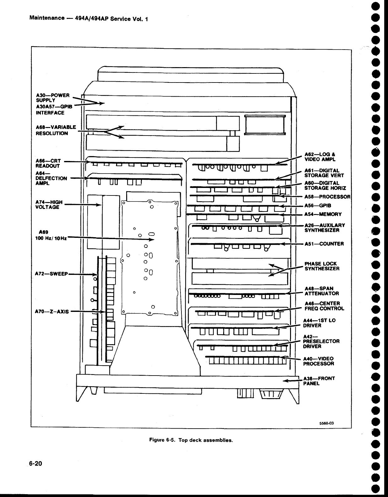
o
a
o
o
a
o
o
o
o
o
o
o
o
c
o
o
o
o
o
o
)
o
o
o
o
c
o
o
o
o
a
O
o
o
o
I
o
o
o
o
O
o
o
o
A30-POWER
St,PPLY
A30A57-GPIB
INTERFACE
A62-LOG &
VIOEO ATPL
A61_DIGITAL
STORAGE YERT
A6O-DIGITAL
STORAGE }IORIZ
As8-PROCESSOR
456_GPIB
A5'-MEMORY
A26_AUXILARY
SYNTHESIZER
A51_COUNTER
A/f0-SPAN
ATTENUATOR
A/16-CENTER
FREO COilTROL
PHASE LOCK
SYNTI{ESIZER
A{2-
PRESELECTOR
ORIVER
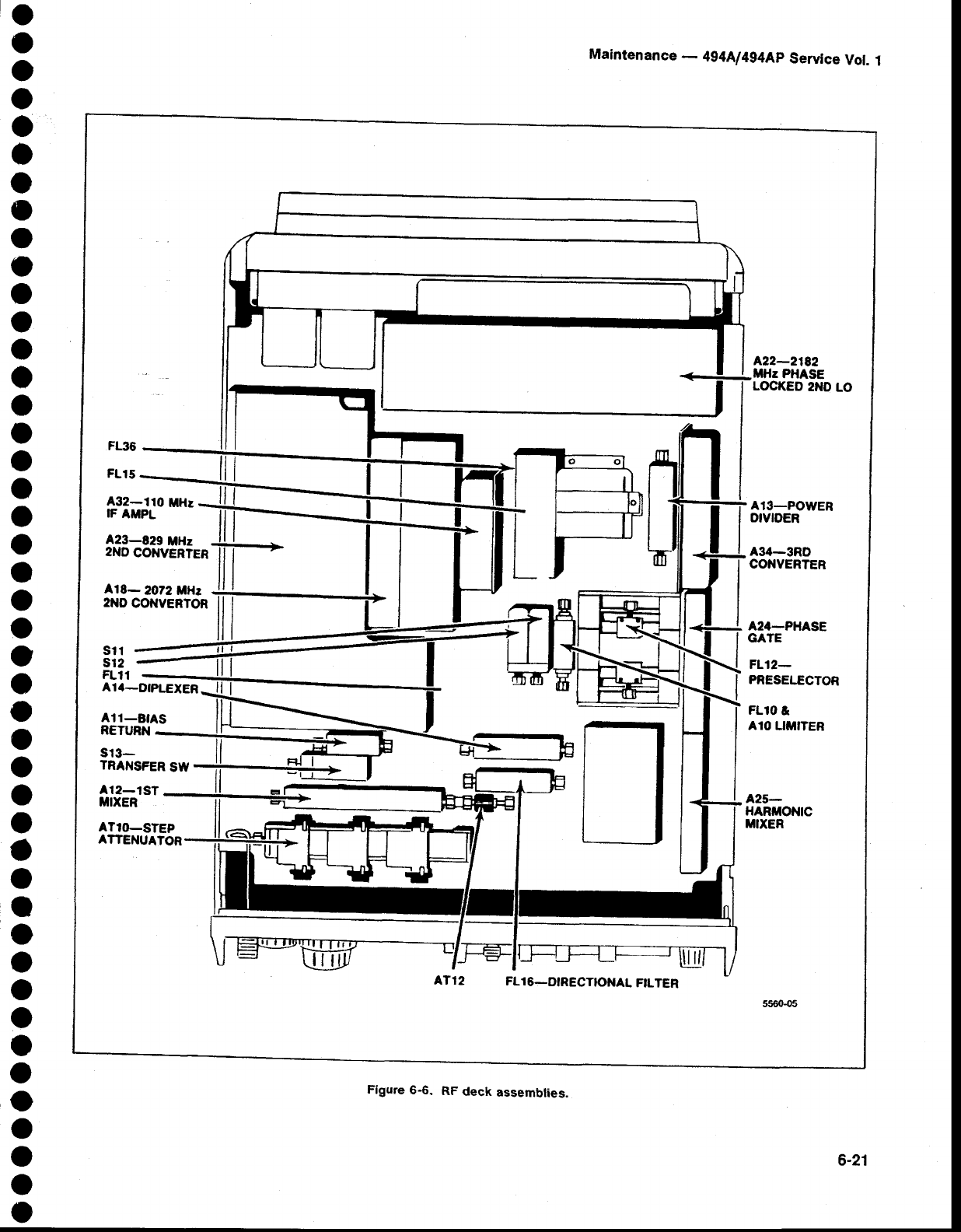
O
o
o
o
o
o
o
o
o
o
o
o
a
o
o
o
o
o
o
o
a
O
o
O
o
o
o
o
o
a
a
o
a
o
a
a
o
o
o
o
o
o
o
I
Maintenance
- 494Al4g4Ap
Service
Vot.
1
FL36
FL15
A32-110 ilHr
IF AMPL 413_POWER
OIVIDER
A23-E29 trtHz
2ND
CO}IVERTER
AlE- 2072 MH:
2ND
CONVERTOR
434-3RD
CONVERTER
A2{-PHASE
GATE
FL12_
PRESELECTOR
FL'O
&
A1O
LIMITER
s11
sl2
FL'1
A1'-DIPLEXER
All-B|AS
RETURN
sr3-
TRANSFER
SIV
il
II
lt
412-1ST
llrxER
ATI{'_STEP
ATTENUATOR
FL1
6_DIRECTIOI{AL FILTER
Figure 6-6. RF deck assemblies.
6-21
Mafntenance
- 494A1494Ap
Service
Vot. 1
Some circuit
boards and
assemblies
must
be
placed
on extenders
to access test points or adjustments.
Before
removing
these
boards
and assembli6s,
the air
bafie attached to the left siderail must also be
r€moved.
Turn
the
power off before
removing
an assembly.
Removing and Installing the GplB Board
The GPIB
board connects
to the GplB port on the
back
panel,
through
a GptB
Extend€r
board (A56A1),
a
ribbon cable (W560),
and a GplB Interface board
(A30A54 in the Power Suppty modute. The GptB
Extender
board edge connector
is clamp€d
to th€ con_
nector
on the GPIB
board by means
of a locking
key
that extends
through
the connector. When
the fly ii
turned,
so it faces inward,
the connector
is clamped.
To release
the connector,
so the GplB board can be
removed,
proceed
as follows:
1. Unscrew
the mounting
screws that hold the
metal shield over the GPIB, processor. and Digital
Storage
boards
and
remove
the shield.
2. Lift
th€ key
to the GptB
Extender
board
connec-
tor up so
it iust clears
the
board
and
turn
it gO
degrees,
so it faces
the rear
of the instrument.
This
will spread
the
connector
so the GPIB
board can now
be pull
from
the connector
on the
Mother
board.
3. Use a board
puller
to pull the GplB board free
from
the Mother
board.
lnstall the
board as tollows:
1. With
the key
tor the GplB Extender
board
con-
nector
turned so the connector
is spread
(top
of the key
facing
to the rear of the instrument),
slide the GplB
board
through
the guides
and onto the Mother
board
connector.
Ensure
that the
board
is well
seated.
2. Turn
the key 90 degrees
to lock
the connectors
of the GPIB Extender board and the GplB board
together. Push
the key
down
to its rest
position.
3. Re-install
the shield
over
the GplB, processor,
and
Digital
Storage
boards.
Removing or Replacing Semi-rigid
Coaxial
Cables
Performance
of the instrument
is easily
degraded if
these connectors
are
loose,
dirty,
or damaged.
The fol-
lowing
procedure
will
help ensure
that
the
connection
is
good
enough
to maintain
proper
performance.
1. Use a 5/1 6 inch
open-end
wrench
to loosen
or
tighten
the connectors. lt is good practice
to use a
second
wrench
to hold
the rigid
(receptacle)
portion
of
the connector
to prevent
bending
or twisting
the cable.
6-22
2. Ensure
that the plug and receptacle
are clean
and
free of any
foreign
matter.
3. Insert
the
plug
connector fully
into
the
receptacte
before screwing
th€ nut
on. Tighten
th€
connection
to g
in-lbs to ensure
that the connection
is tight. Do not
overtighten ('l5 to 20 in-lbs)
because
this can damage
the connector.
Replacing
lhe Dual Diode
Assembly
in the 1st Mixer
The diode subassembly
that houses
the Schottky
mixer diodes permits easy field replacement of the
diodes. The subassembly
is secured in place
with
four
0-80
screws.
An
8-32
threaded hole is provided
to facil-
itate insertion
and removal of the subassembly.
There
are three contact
points
located on
the
substrate
side
of
the subassembly.
Use
care
to ensure
proper
fit when
mounting and orienting
these contacts in the mixer
assembly. Insertion
and removal
of the subassembly
more
than twice is not recommended
due to th€ gold-
ribbon
attaching
technique
used in
fabrication.
' A tuning
screw is adjusted
to null a start spur
on
Band
1. This
tuning screw is mounted
through the
top
of the diode asssembly,
adjacent
to the 8-32 hole. lf
adjustment
of this screw
is warranted. care should
be
taken to not force the tuning
screw after it bottoms out
on
the
surface
of the
quartz-suspended
substrate.
The diode assembly is packaged
in a static-free
package.
Keep
the diode
subassembly in this
package
until ready to install. The following
should be used
when replacing
this
assembly.
The diodes are beam-lead devices,
mounted
on a quartz-suspended
substrate.
These diodes are extremely sensitive to
static electricity
discharge. Refer to the
caution note on static discharge
at the
beginning
of this section. Do not expose
the diode
assembly
to
RF fields.
1. Loosen and disconnect
the three
coaxial
cable
connections at the
1st
converter
assembly.
2. Remove
the two mounting
screws,
and remove
the
assembly
from the
instrument.
3. Remove
the four 0-80
screws that
hold the diode
subassembly
in the 1st Converter,
and insert
a 8-32
screws into
the threaded
hole
provided
in the
center of
the diode
assembly.
4. Lift the diode
assembly out
of the mixer
assem-
bly by
m€ans
of the 8-32
screw, then remove
the
screw.
o
o
o
o
o
o
o
o
o
o
o
o
o
o
o
o
o
a
o
o
o
o
o
O
o
O
o
o
o
o
I
O
o
o
o
O
o
o
o
o
o
o
o
o
o
o
o
o
o
o
o
o
o
o
o
o
o
o
o
o
o
o
o
o
o
o
a
o
o
o
o
o
o
o
o
o
o
o
o
o
o
o
o
o
o
o
o
o
5. Open
the
diode
package.
Use
a pair
of tweezers
to grasp
th€
diode
assembly
by its side,
and place
it on
a static-free
surface. Grasp
t-he
side of the'"rr"rOty
with^the
fingers.
Avoid
coniact
with
the
diodes. Insert
the 8-32
screw.
6, Orient
the diode
assembly
so the three
contact
tips are arigned
with their respictive contacts
in the
mixer;
then,
using
the index fingers
of both
hands
so
equal pressure
is applieO,
presJ
the subassembty
into
place.
7, Insert
the four mounting
screws,
then replace
and tighten
the three coaxial
ionnectois to g in-lbs.
Remount
the lst Conv€rter
assembly
Oy instatting
itre
two mounting
screws
that hold
ttre
aisembty
to th; RF
deck.
-. . 8. The Spectrum Analyzer may not meet the
flatness
specification
after the Duat
CIode
assembly
is
replaced. Refer
to MATNTENANCE
ADJUSTMENTS
in
this_ seetion
for a procedure
for adjusting
converter
bias
and
flatness.
Replacing the Crt
1. Remove
the snap_in
printed
bezel
and crt tight
filter.
. 2: Use an g/64 inch AllEn
wrench
to remove
the
four
bezel
screws,
unplug
and
remove
the inner
bezel.
3. Unsolder
the ground
wire from the front panel
casting
and unplug
the crt cables
at their respective
?oarg_
connections
(High Voltage module,
Deflection
Amplifier
board,
and
Z-Axis
UoarO;.
4. Slide
the
crt,
with
its shletd,
out
through
the
front
panel.
5. Remove
the
crt shield
as
follows:
a. Remove
the tube base cap and unplug
the
socket.
b. Remove
the
two side
screws
that
hold
th€
upper
shield
in
place,
then
remove
the shield.
c. Loosen
the
screws
that clamp
the
plastic
bracket
around
the crt, then remove
the bracket.
. 6. Jnstall
the plastic
bracket so the back on the
ctamp
is 5.07
inches
from the back of the cn socket
guide.
- 7. ReplacE
the crt shield plus
the socket
and
base
shield
by reversing
the
removal procedure.
The
finished
crt
^assembly
length.
with cap installed,
must equal
11.05
inches.
lf it
is
longer,
the assembly
may
short
cir_
cuit the Deflection
Amplifier
circuit boird when it is
installed.
. 8.. Place
_
the spectrum
analyzer
on its rear panel
then
loosen
the
four
crt blue
ptastic
mounting
blocks
on
the
front
casting
so
they
can
be readily
positioned
when
the crt is installed.
Maintenance
- 4g4Ll4g4Ap
Service
Vol. 1
9. lnstall
the crt with shield
assembly
through
the
front
panel;
seat
the wedges
on the siOe
of the crt,
into
the
blue
plastic
rnounting
blocks.
10. Position
the
cast bezel
and implosion
shield
in
place
to €nsure
that
there
is clearance
between
the
crt
face and the bezel, fl'he bezel must bottom on the
front
casting.)
It. is very important
that the four mounting
blocks are loose enough so the bezel
retaining
screws
can be tightened
without
the bezel
touching
the crt face. lf not the
crt or the
bezel
may crack
when
the
screws
are
tightened.
11. Remove
the bezel and tighten
the mounting
block
screws
evenly
in
a cross
pattem
to approximatel!
8 in-lbs. Make
sure
the crt stays
centereO
in tf,e Utui
plastic
mounting
blocks
as
the screws
are
tightened.
12. Replace
the bezel
and implosion
shield,
recon-
nect cables
to their respective
board
connectors,
and
resolder
the
ground
lead
to its terminal.
13. Replace
crt light
filter
and
snap-in
printed
bezel.
Repairing the Crt Trace Rotation Coil
The
trace
rotation
coil is part of the
crt assembly.
tf
the coil
is damaged
beyond
repair,
the crt with
the coil
must
be
replaced.
.lf the 'finish"
(red)
lead
is broken,
remove
the tape
and
unwind
one
or two tums so it can
be respliced
and
solder€d
to the
lead
wire. Rewind
and
retape.
.lf the "start"
(black)
lead is broken
and the lead is
too short
to re-splice,
atempt to fish
out
the
broken
end
so one or two turns can be unwound,
re-splice
and
solder
to the
lead;
then rewind
and
retape.
Front
Panel
Assembly Removat
It is not
necessary
to remove
the front
panel
assem-
bly to replace
any of the push buttons. (Refer
to
Replacing
Front Panel
pushbuttons,
that follows this
procedure.)
The crt is removed
with the front-panel
assembly,
1. Set
the instrument
upright on
its rear
panel,
then
unscrew
and remove
thg mounting
nuts and washers
for the RF INPUT,
EXT
MIXER,
lst Lo oUTPUT. and
2nd
LO
OUTPUT connectors.
2. Remove
the two screws
that hold
the
front
panel
to the RF
deck (center
and
left side).
6-23
Maintenance
- 4g4A/4g4Ap
Seruice
Vot.
1
- 3. Unplug
the CAL
OUT
coaxial
cabte
from
the
grd
Converter;
then disconnect
the five crt cables
from the
Z-Axis/RF Interface, High Voltage module, and
Deflection
Amplifier.
4. Looking
at the
top of the instrument,
remove
the
one screw
that
holds
th€
front panel
to the side
extru_
sion between
the crt and the right side
of the instru_
ment. Remove
the four
screws
that
hold
the
tront
panel
to the
side
rails.
5. Pull
the front
panel
up and
off
the
Mother
board.
Replace
the front panel
by reversing
th€ removal
procedure.
Front-Panel Board Removal
A replacement
Front panel board comes
with switches and controls for program-
mablo diffErent
versions
of the spectrum
analyzer. Before replacing an existing
board, remove
the switches
and controls
on
the new
board
that are not used
on
the par_
ticular
version
of the
instrument.
1. Remove
the front panel
assembly
as previously
described,
then
remove
all
the knobs.
2. Place
the front
panel
on its face
and
remove
the
eleven
circuit
board screws plus
the screw
that heat_
sinks and holds U6090
on the board. Note that the
screw
next
to
the
connector
plug
has
a fiber
washer.
3. To prevent
tosing
the grounding
rings or bush_
ings, between
the front panel
controls
and the front
panel
casting,
hold th€ circuit
board
against
the front
panel
casting
while
turning
the
complete
assembly
so it
r€sts on
the
base of the
crt
assembly.
4. Gently
lift the casting
from the circuit board.
Ensure
that
the grounding
rings
remain
on the shaft
of
all controls
as
the
casting
is removed.
Reverse
the r€moval procedure,
ensuring
that the
fiber
washer
is on the board
screw
next
to the connec_
tor plug. This
waEher
prevents
the
screw
from
shorting
a circuit
board run
to the front
panel
casting.
Replacing
Front Panel
pushbutton
Switches
Removal
of the
front panel
assembty
is not required
to replace
any pushbutton
switch.
The procedure
fol_
lows:
1. Remove
the front panel knobs. Loosen and
remove
nuts and washers
for the RF lNpUT,
EXTER_
NAL
MIXER,
and
the 1st
and
2nd
LO
connectors.
2. Remove the screw under the CENTER
FRE_
QUENCY
tuning
knob
that holds
the panel
to the
front
panel
casting.
3. Loosen
the black
screws
through the crt bezel
so the
panel
can be moved enough
to lift it off
the
cast-
ing.
4. Unplug
and
replace
the desired
switches.
Main
Power
To avoid
damage
to the Mother
board con-
nector J5041 and lnterface connector
J1034, during
removal
or installation of the
Power Supply module,
use the following
procedure.
1. Disconnect
the power cord and remove
the
instrument cover.
2. On the circuit board side of the instrument.
unplug
the coaxial
cable
connector
P620 from
the Log
and Video Amplifier
assembly. On the RF deck side
disconnect
th€ plug
for the
cable
to the Reference
Lock
assembly,
at the lower
right comer
of the
Power
Supply
module.
3. For
programmable
instruments, remove
the
cable
clamp
for the GPIB
interconnect
cable and
unplug P560
to the GPIB Extender
board.
4. Remove
the three
screws
that hold the power
module
to the RF deck flange
(bottom
right side),
then
remove
the four screws that hold the power supply
module
to the side rails.
5. With the instrument
RF deck on the near side,
pull the left side
of the power
module trom its side-rail
(no more than 1.5 inch). Now grasp both
sides
of the
module and lift to separate
the module from
the Mother
board.
Because
C6111 and C6101
discharge
very
slowly.
hazardous
potentials
exist
within
the
pow€r supply
for several
minutes
after
the
power switch is turned off. A relaxation
oscillator, formed
by C5113,
R5111,
and
DS51 12, indicate
the presence
of voltages
in the circuit until
the potential
across
th€
filter
capacitors
is below B0
V.
6. Loosen
and remove
the two screws that hold the
mounting bracket for P361
. Lift the cover off the
module
and unptug P3045
to the Fan Drive board.
The
power
supply should
now
be
accessible.
Supply Module
Removal
[eAUloNl
o
o
o
o
o
o
o
o
o
o
o
o
o
o
o
o
o
o
o
o
o
o
o
o
o
o
o
o
o
o
o
o
o
o
o
o
o
o
o
o
o
o
o
o
6-24
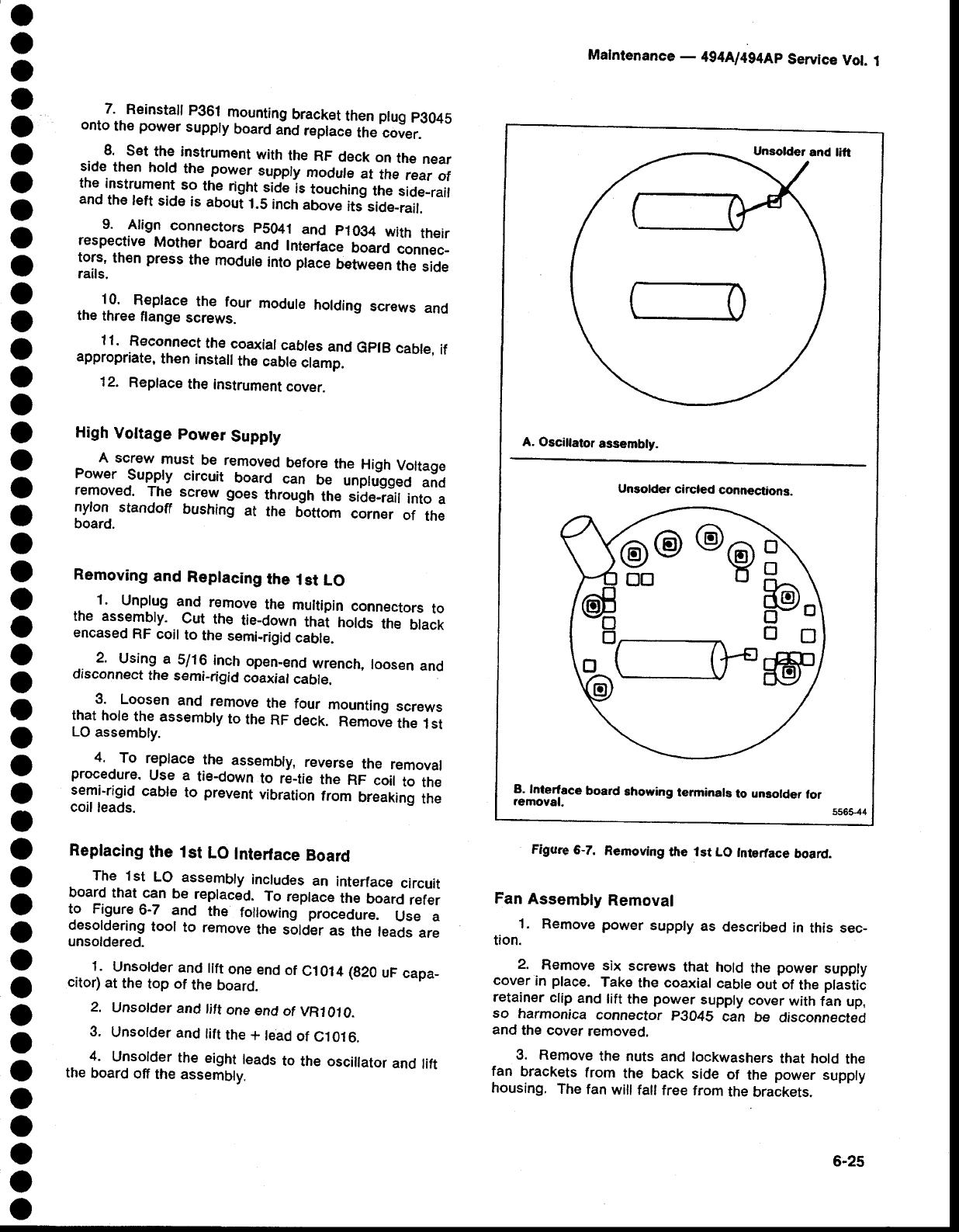
o
o
o
O
a
o
o
o
o
o
o
o
o
o
o
o
o
o
o
o
o
o
o
o
o
o
o
o
o
o
o
o
o
o
o
o
o
o
o
o
o
o
o
o
7. Reinstall
p361.
mounting
bracket
then
ptug
pg045
onto
th€
power
supply
board
anO
repacJ
the
cover.
8. Set
the instrument
with
the
RF
deck
on
the
near
side.
then hold the power supply
module
at the rear of
the
instrument
so the right
side
is
touctring
the
side_rait
and
the
teft
side
is aboui
1.5
inch
above
iti side-rait.
9. Align connectors
p5041
and p1034 with their
respective
Mother board
and Interface
board
connec-
tors'
then
press
the
modure
into
prace
beh^/een
the
side
rails.
10. Replace
the four module
holding
screws
and
the
thre€
flange
screws.
11. Reconnect
the.coaxial
cables
and
GplB
cable,
if
appropriate,
then
installthe
cable
clamp.
12. Replace
the
instrument
cover.
High Vottage power Suppty
A screw
must be removed
before
the High
Voltage
Power luqpty circuit board can Oe unplugged
and
removed.
The screw
goes
througt tt" iib"-rail into a
nylon standoff bushing
at the bottom corner of the
board.
Removing
and Replacing
the lst LO
. 1. Unplug
and remove
the multipin
connectors
to
the assembty.
Cut the tie_down
thai hoids the black
encased
RF
coil
to the
semi-rigid
cable.
.. 2. Using
a S/1
6 inch
open-end
wrench,
toosen
and
disconnect
the
semi-rigid
coaxial
cable.
3. Loosen
and remove
the four mounting
screws
that
hole
the assembly
to
the
RF
deck.
Remove
the
1st
LO
assembly.
4. To replace
the assembly,
reverse
the removal
procedure.
Use a tie_down
to ri-tie the RF coil
to the
semi-rigid
cable
to prevent
vibration
from breaking
the
coif
leads.
Replacing
the 1st LO Interface
Board
The 1st LO assembly
includes
an interface
circuit
board
that
^c1n
be reptaced.
To replace
the
board
refer
to Figure
6-7 and the following
procedure. Use a
desoldering
tool to remove
tne
sotOlr
as the teads
are
unsoldered.
1. Unsolder
and
tift
one_end
of
C1014
(g20
uF
capa_
citor)
at the
top of the
board
2. Unsolder
and
tift
one
end
of
VRl010.
3. Unsolder
and
lift
the
+ lead
of
C1016.
4. Unsolder
the eight
leads
to the oscillator
and
lift
the
board
off
the
assembly.
Malnfenance
- 4g4Ll4g4Ap
Service
Vot.
1
Figure
6-7. Removing
the lst LO Intertace
board.
Fan Assembly Removal
1. Remove
power
supply
as
described
in
this sec_
tion.
2. Remove
six screws
that hold
the power
supply
cover
in place.
Take
the coaxial
cable
out
of
the
plastic
retainer
clip
and
lift
the
power
supply
cover
with
fan up,
so harmonica
connector
pgO4S
can be disconnected
and
the cover
removed.
3. Remove
the nuts
and lockwashers
that hold
the
fan brackets
from the back side of the power
supply
housing.
The
fan
will
fall
free from
the
brackets.
A. Oscillator assembly.
Unsolder circled connections.
B. Interface board showing terminals to unsolder for
removal.
tr\
o\
pJ
trD
ff
@o
@@
DOU
6-25
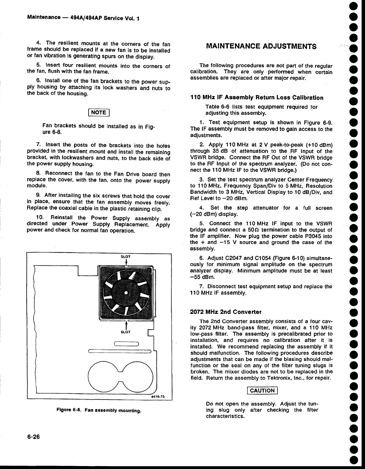
Fan
brackets
should
be installed
as in Fig-
ure
6-8.
7. Insert
the posts of the brackets
into the holes
provided
in the resilient
mount
and
install
the remaining
bracket, with
lockwashers
and
nuts,
to the
back
side
of
the
power
supply
housing.
8. Reconnect
the fan to the Fan Drive
board
then
replace
the cover,
with
the fan, onto
the power
supply
module.
9. After
installing
the six
screws
that hotd
the
cover
in place,
ensure
that the fan assembly
moves
freely.
Replace
the coaxial
cable
in
the
plastic
retaining
clip.
10. Reinstall the Power Supply assembly as
directed under Power Supply Replacement. Apply
power
and
check
for normal
fan
operation.
Maintenance
- 494A1494Ap
Servlce
Vol.
I
4. The resilient
mounts
at the corners
of the fan
frame
should
be replaced
if a new
fan is to be installed
or fan vibration
is
generating
spurs
on
the
display.
5. Insert
four resilient
mounts
into the corners
of
th€ fan, flush
with
the
fan
frame.
6. Install one
ol the
fan
brackets
to the
power
sup-
ply housing
by attaching
its lock washers
and nuts to
th€
back
of the housing.
MAINTENANCE
ADJUSTMENTS
The following procedures are not part of the regular
calibration. They are only performed when certain
assemblies
are replaced or after major repair.
110 MHz
lF Assembly Return Loss Calibration
Table
6-6 lists test equipment
required
for
adjusting this assembly.
1. Test equipment
setup is shown
in Flgure
6-9.
The lF
assembly
must
be
removsd
to gain
access
to the
adiustments.
2. Apply
110 MHz at 2V peak-to-peak
(+10
dBm)
through 35 dB of attenuation
to the RF Input of the
vswR bridge. connect the RF out of the
vswR bridge
to the
RF Input of the
spectrum analyzer. (Do
not
con-
nect
the 110 MHz
lF
to
the vswR bridge.)
3. Set
the
test spectrum
analyzer Center Frequency
to 110
MHz,
Frequency
Span/Div to 5 MHz, REsolution
Bandwidth
to 3 MHz, Vertical Display
to 10
dB/Div, and
Ref Levelto
-20 dBm.
4, Set the step attenuator for a full screen
(-20 dBm) display.
5. Connect the 110MHz lF input
to the vswR
bridge
and connect a 50O termination to the output of
the lF amplifier. Now plug
the power
cable
P3045
into
the + and -15 V source and ground
the case of the
assembly.
6. Adjust
C2047
and
Cl054 (Figure
6-10) simultane-
ously for minimuh signal
amplitude
on the spectrum
analyzer
display. Minimum
amplitude must
be at least
-55 dBm.
7. Disconnect
te6t
equipment setup and replace
the
110 MHz
lF
assembly.
2072MHz 2nd Converter
The
2nd
Converter assembly
consists of a four cav-
ity 2072
MHz band-pass filter,
mixer, and a 110 MHz
low-pass filter. The assembly is precalibrated prior
to
installation, and requires no calibration after it is
installed. We recommend
replacing the assembly
if it
should
malfunction. The following
procedures
describe
adjustments
that can be made
if the biasing
should mal-
function
or the seal on any of the
filter
tuning slugs
is
broken. The mixer diodes are not
to be replaced in the
field. Return the
assembly
to Tektronix, lnc., for repair.
Do not open the assembly. Adjust the tun-
ing slug only after checking the filter
characteristics.
o
o
o
o
a
o
o
o
o
o
o
o
o
o
o
O
o
o
o
o
o
o
o
o
o
o
o
o
o
o
o
o
o
o
O
o
o
O
O
o
o
o
o
o
6-26
Flgure
5{. Fan
assembty
mounting.
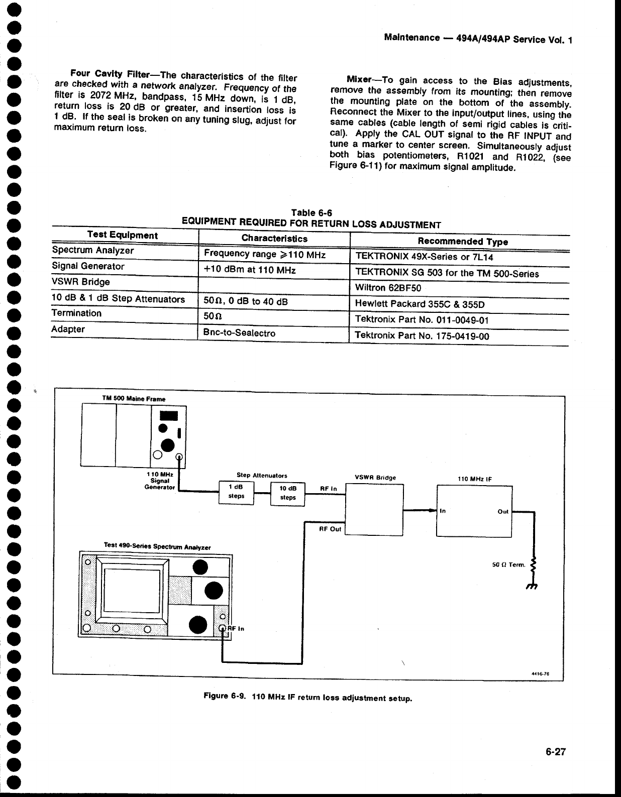
o
o
o
o
o
o
o
o
o
o
o
o
o
o
a
o
o
o
o
o
o
o
o
o
o
o
o
o
o
o
o
o
o
o
o
o
o
O
o
o
o
a
o
o
Four Cavlty Fllter-The characteristics
of the filter
are checked
with a network analyzer.
Freguency
of the
filter is 2A72MHz,
bandpass,
t-S
Ul-lz down, is 1
dB,
return
loss is 20
dB or greater,
and insertion
loss is
1
clB. lf the
seal
is broken
on
any
tuning
slug,
adjust
for
maximum
return
loss.
Malntenance
- 494A/494Ap
Service
Vol. 1
Mlxer*To gain access to the Bias adjustments,
rernove
the assembly
from its mounting;
then remove
the mounting ptate on the bottom of the assembly.
Reconnect
the Mixer
to the input/output
lines,
using
the
same
cables
(cable
length
of semi
rigid
cables
is iriti_
cal). Appty
the CAL
OUT signat
to the RF INpUT
and
tune
a rnarker
to center
scr€en, Simultaneously
adjust
99th bjas porentiometers,
R1021 and R1022,
liee
Figure
6-11)
for maximum
signal
amplitude.
Table
6-6
EOUIPMENT
REQUIRED
FOR
RETURN
LOSS
ADJUSTMENT
Test
Equlpment Recommended
Type
Spectrum
Analyzer TEKTRONIX
49X-Series
or 7L14
Signal
Generator TEKTRONIX
SG
503 for the TM
S0O-Series
VSWR
Bridge Wiltron
628F50
10
dB
& 1 dB
Step
Attenuators Hewlett
Packard
355C
&
g55D
Termination Tektronix
Part
No.
011-0049-01
Adapter Tektronix
Part
No.
175-0419-00
Tll 50O M.ine F.rme
Test fg0-S€ries Spoctrum
Anatyz€r
a{te76
Frequency
range
)110 MHz
+10
dBm
at
110
MHz
50O,
0 dB
to 40
dB
Figure 6-9. 110
MHz lF return
loss adjustment setup,
6-27
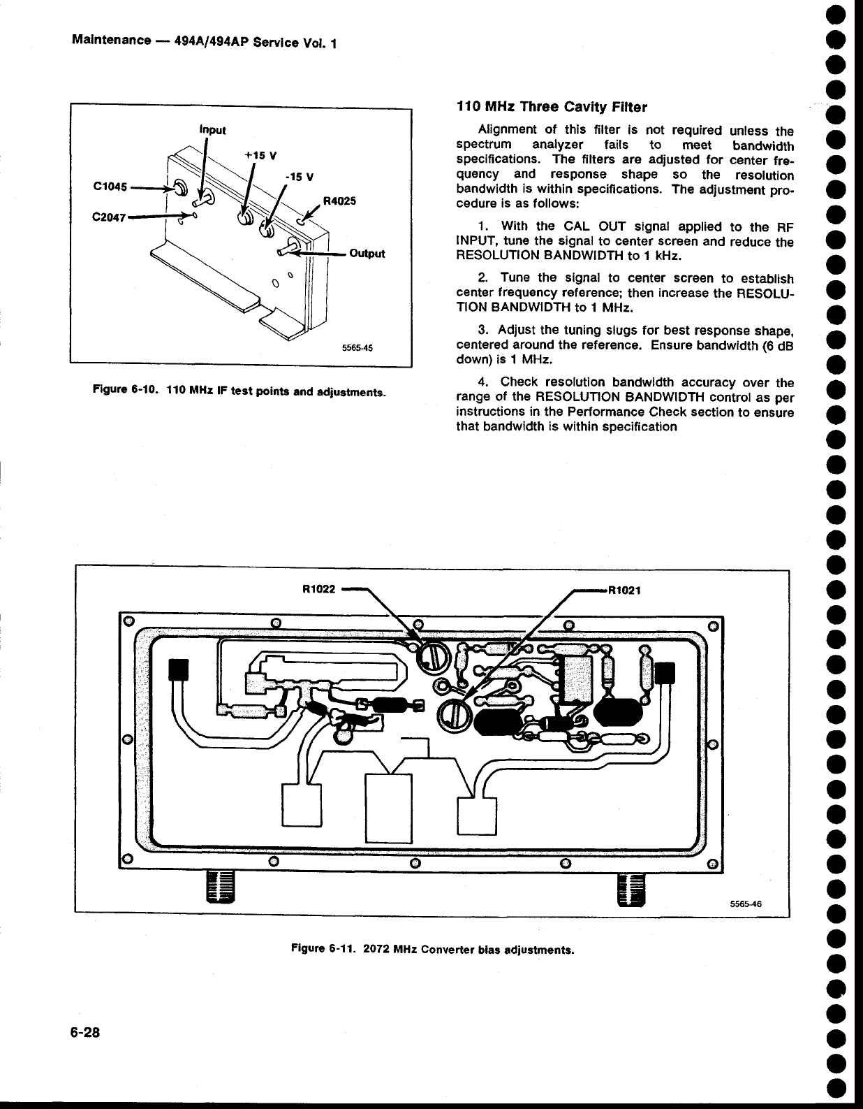
Mafntenance
- 494A1494Ap
Servtce
Vot.
1
Input
c1045
c2047
Flgure
6-10. 110
MHz
lF
test
poinb and
adiuetmenb.
110 MHz Three Cavity Filter
Alignment
of this filter is not required
unless
the
spectrum analyzer fails to meet bandwidth
specifications.
The filters are adiust€d
for center
fre-
quency and response shape so the resolution
bandwidth
is within
specifications.
The
adjustment pro-
cedure is as
follows:
1. With the cAL ouT signat
apptied
to the RF
INPUT,
tune
the signal
to center screen
and
reduce
the
RESOLUTION BANDWIDfi to 1 kHz.
2. Tune the signal to center screen
to establish
center frequency
reference;
then
increase
the RESOLU-
TION
BANDWIDTH
to 1 MHz.
3. Adjust
the
tuning
slugs
for best response
shape,
centered around
the
reference.
Ensure
bandwidth
(6
dB
down)
is 1 MHz.
4. Check resolution
bandwidth accuracy over the
range
of the RESoLUTIoN
BANDWIDTH controt
as per
instructions in
the Performance
Check
section
to ensure
that bandwidth
is within specifieation
o
o
o
O
o
o
a
o
o
o
o
o
o
o
o
a
o
O
o
o
o
o
o
o
o
o
a
o
o
o
O
o
o
o
o
O
o
o
o
o
o
o
o
o
6-28
Figure 6-11. 2O72
MHz Converter blas adiustments.
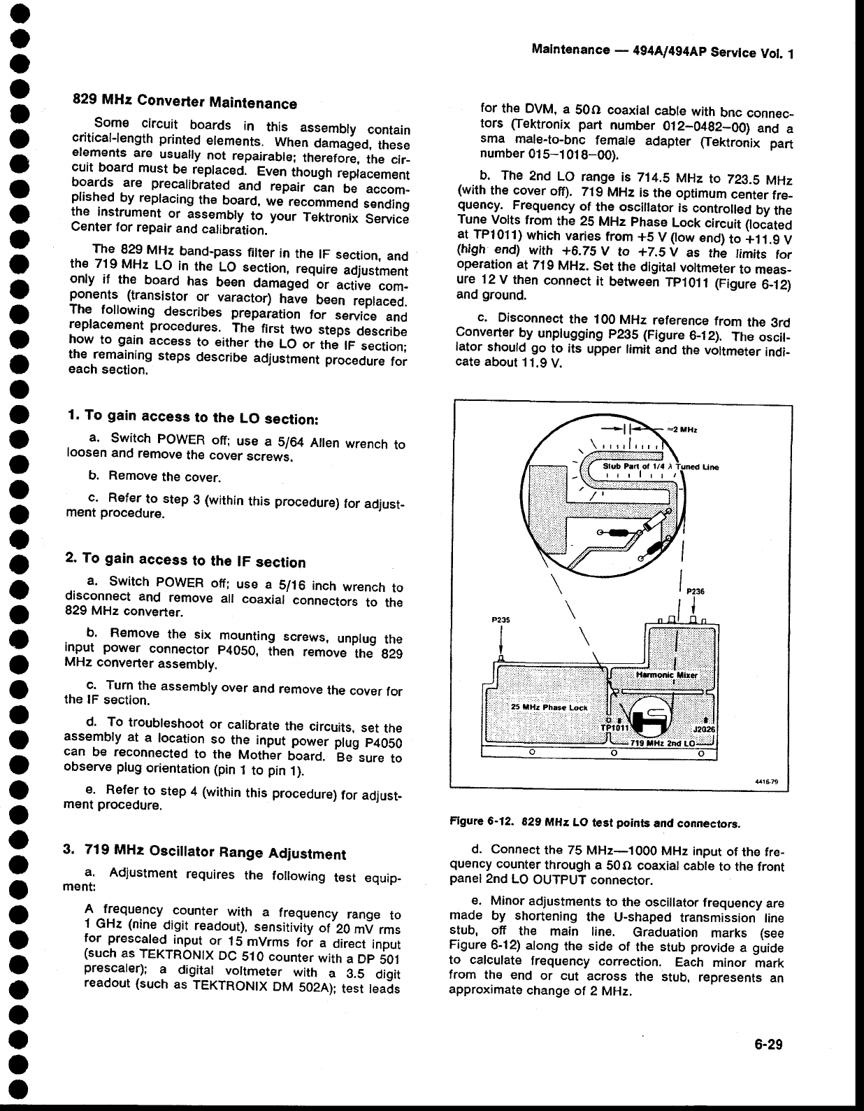
o
a
o
o
t
o
t
o
o
I
o
a
o
t
a
O
a
o
o
o
a
a
o
o
o
o
O
o
o
o
o
o
o
o
o
o
o
o
o
o
o
a
o
o
829 MHz Converler Maintenance
Some circuit boards in this assembly contain
critical-length
printed
elements.
When
damaged,
these
elements
are usually
not repairable;
therefore,
the cir_
cuit board
must
be replaced.
even
itroujfr
repfacement
bgards .are precalibrated and ,"p"i, "-"n be accom_
plish.ed.by
replacing
the
board,
we recommend
sending
the instrument
or assembly
to your Tekironix
Service
Center
for repair
and
calibrition.
-
The 829
MHz
band-pass
filter
in the lF section,
and
the 7'l9 MHz
LO in the
-Lo section,
require
adjustment
only if the board has been damaged'J, ""tiu" "o*-
ponents (transistor
or varactor)
hive been reptaced.
The following
describes
prepaiation
foi service
and
replacement
procedures.
The first two steps
describe
how to gain access
to either
the LO or the lF section;
the.remaining
st€ps
describe
adjustment
procedure
for
each
section.
1. To gain access to the LO section:
a. Switch
POWER
ofi; use a 5/64
Ailen
wrench
to
loosen
and
remove
the
cover
screws.
b. Remove
the cover.
c. Refer
to step
3 (within
this procedure)
for
adjust-
ment
procedure.
2. To gain access to the lF section
a. Switch
POWER
off; use a 5/16 inch
wrench
to
disconnect
and remove
all coaxial connectors
to the
829 MHz
converter.
b. Remove
the six mounting
screws,
unplug
the
input power connector
P4OSO,
ihen remove
the g2g
MHz
converter
assembly.
c. Turn
the
assembly
over
and
remove
the
cover
for
the lF
section.
d. To troubteshoot
or calibrate
the circuits,
set
the
assembly
at a location
so the input power
plug
p4050
can be reconnected
to the Mother
boarO.
Be sure
to
observe plug
orientation
(pin
1 to pin
1).
e. Refer
to step
4 (within
this procedure)
for adjust-
ment
procedure.
3. 719 MHz Osciilator
Range
Adjustment
a. Adjustment
requires
the foilowing
test equip-
ment:
| ^frequency
counter with a frequency
range to
1 GHz (nine
digit readout),
sensitivity
of 20
mV rms
for prescaled
input
or 15
mVrms
tor a direct
input
(such
as
TEKTRONIX
Dc 510 counter
with
a Dp
501
pres.calee;
a digital voltmeter with a g.5 digit
readout (such
as TEKTRONIX
DM 502A);
test teads
Maintenance
- 4g4N494Ap
Servtce
Vol.
1
for th€ DVM,
a 50O coaxial
cabte
with
bnc
connec_
tors ffektronix part number
012-04g2_00)
and a
sma male-to-bnc f_emale
adapter Cfektronix part
number
015-1018-O0).
b. The
2nd LO range
is 714.5
MHz
to 223.5
MHz
(with
the cover
off). 71g
MHz
is
the optimum
center
fre_
guen!{. .
Frequency
of the osciltator
is controlled
by
the
Tune
Volts
from
the 25
MHz
phase
Lock
circuit
ltoiateO
at
TPl011)
which
varies
from
+5
V
(low
end)
to +11.g
V
(high end) with +6.75
V to +2.5 V as the timits for
op€ration
at 719
MHz.
set the
digital
voltmeter
to meas_
ure 12
V then
connect
at
between
Tplolt (Figure
6-12)
and
ground.
c. Disconnect
the 100
MHz
reference
from
the
grd
Converter
by unplugging
p235
(Figure
6-12).
The
oscit_
lator
should
go to its upper
limit and
the
voltmeter
indi-
cate
about
1
1.9
V.
Figure
6-12.
829
MHz
LO
test
points
and connectors.
d. Connect
the 75
MHz-1 000 MHz input
of
the fre-
quency
counter
through
a 50O coaxial cable
to the front
panel
2nd
LO
OUTPUT
connector.
e. Minor
adjustments
to the
oscillator frequency
are
made
by shortening
the U-shaped
transmission
line
stub, off the main line. Graduation
marks (see
Figure
6-12)
along
the side
of the stub
provide
a guide
to calculate
frequency
correction. Each minor mark
from the end or cut across the stub, represents
an
approximate
change
ot 2 MHz.
6-29

Maintenance
- 494A1494Ap
Service
Vot.
1
_ Check
the freguency
by noting
the reading
on the
frequency
counter. lf above 729.900
MHz, the stub
must be lengthened.
Solder a bridge
across
the cut
"q r.e"!99\
frequency.
Nominal
frequency
for an
uncut
stub
is 710
MHz.
f. Shorten the line so the frequency
is near
723.500
MHz. For example:
The frequency
difference
between
the desired and thE actuat
divideci
Oy
Z
Unz,
equals
the number
of minor
divisions
from
thE line
end
for the new
cut. Make
a cut across
the
line and
check
that the new frequency
is between
723.100
MHz and
723.900
MHz.
Repeat
as necessary.
g. Cover
the 719
MHz
osciltator
cavity
with
the
g29
MHz Converter
cover, press down to ensure good
shielding,
and note the frequency readout of the
counter.
Frequency
should
fall within
723.600
MHz and
724.400
MHz.
h. Reconnectp2S4
(100
MHz)
andp237
(2i82
MHz)
and confirm
that phase
lock
is operating
by noting
thai
the voltage
on Tp1011
is between
O.7SV
and
7.5V.
This completes
the adjustment
of the 71gMHz Lo.
Replace
the cover
and reinstall
the g2g
MHz converter
assembly.
4. 829 lr/lHz
Coaxial
Band-pass
Fitter
Adjustment
This
procedure
is necessary
if the position
of one of the variable
capacitor
loops (tabs)
has been altered,
changing
the bandpass
characteristica
of the
filter.
a. Test
equipment
required:
Spectrum
analyzer
with tracking
generator
(such
as
a TEKTRONIX
49X-Series
Spectrum
Analyzer
with
TR 503
Tracking
Generator,
or 7L,t4
with i TR 502
Tracking
Generator);
Frequency
Counter (such
as a
TEKTRONIX
DC 510 Counter
with a Dp 501
pres_
caler);
and
a Beturn
Loss Bridge (such
as a Wiltron
Model62BF50.)
b. Unsolder
and reconnect
the jumper,
on the g2g
MHz
Amplifier
board,
to the
test peltola
jack
J1029
(see
Figure
6-13).
c. Connect
the spectrum
analyzer,
tracking
genera-
tor, and frequency
counter
together
as a system,
with
the frequency
counter connected
to the Auxiliary RF
Output of
the
tracking
generator
(see
Figure
6-14).
-
\
\
Figure 6-13. 829
MHz
ampllfier
test
iack
and
iumper.
d. Connect the spectrum
analyzerltracking
genera-
tor system through
the return
loss
bridge to the
Peltola
jack (J1029)
on the 829MHz amplifier
board {see
Figure
6-14).
Reconnect
P235
(100
MHz
reference
sig-
naf) and P2g7
(2182
MHz input)
to the LO
section
of the
converter.
Terminate
the 110 MHz Output
(J2 21
connector
with 50o, using a bnc-to
Sealectro
adapter
and 20
dB
bnc attenuator. Pull
the
lF SELEGT
line
high
by
switch-
ing
to
band 2
(1.7-5.5
GHz).
e. Set the test spectrum analyzer
Reference
Level
to -20
dBm,
Vertical
Display
mode
to 2 dBldiv, Resolu-
tion Bandwidth to 300
kHz, and Freq Span/Div to
20
MHz. Tune
the Center Frequency for a readout of
829.00 MHz
on
the frequency counter.
f. Adjust the 114 wavelength
lines in the filter in
sequence, starting
with
the
resonator
at the 829 1 MHz
input
(see
Figure 6-15),
Adjustment is made
by
shorting
the adjacent resonator
to ground
with a low inductance
conductor, such as a broad blade screwdriver,
then
bend
the loop
or tab of the respective
stub with
a non-
metallic
tuning tool to change
the series
capacitance
of
the resonator.
o
a
o
a
a
o
a
o
o
a
a
a
o
a
o
a
o
o
o
O
o
o
o
o
o
o
o
o
o
o
O
o
o
o
o
o
o
o
o
o
o
o
o
o
6-30
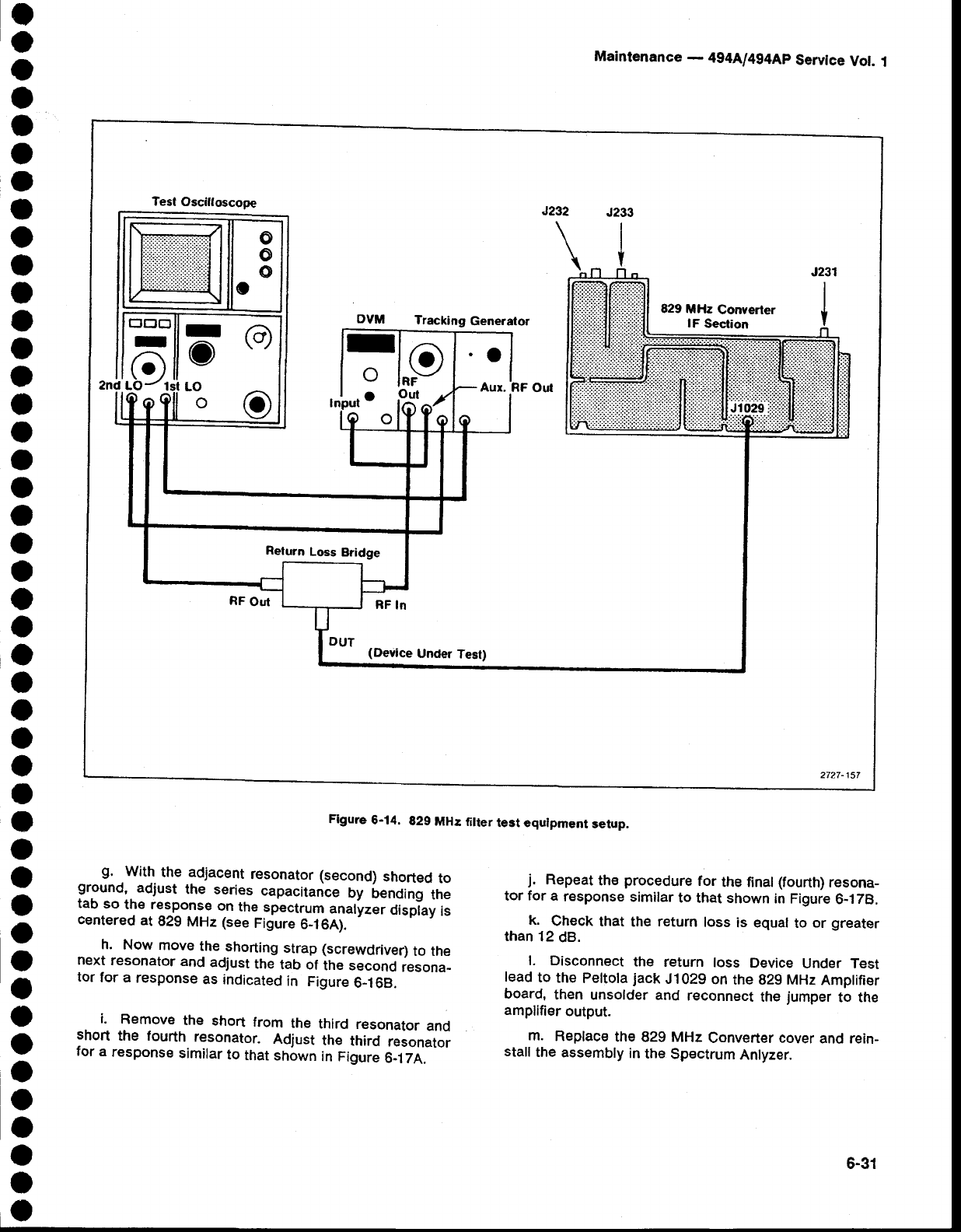
o
o
o
o
o
o
I
o
o
O
o
a
O
a
t
o
a
o
o
a
O
o
a
o
a
o
t
o
a
O
I
o
I
o
o
o
o
o
o
o
o
a
o
o
g. .With the adjacent resonator (second) shorted to
ground, adjust the series capacitance by benOing
tne
tab so the response on the_spectrum
analyzer
display
is
centered
at 829 MHz (see
Figure
6_16A). -
h. Now move the shorting strap (screwdriver)
to the
next resonator and adjust the tab of the second resona_
tor
for a response
as indicated
in Figure
OiOe.
i. Remove the short from the third resonator and
short the fourth resonator. Adjust the third resonator
for a response similar
to that snown in Figure 6-1
7A.
Flgure 6-14. 829 MH: filter test equlpment setup.
Maintenance
- 494[l4g4Ap Servlce
Vot.
I
j. Repeat
the
procedure
for the final
(fourth)
resona-
tor for
a response
similar
to that shown
in Figure
6-178.
k. Check
that the return
loss
is equal
to or greater
than
12
dB.
l. Disconnect
the return loss Device
Under Test
lead
to the
pettota
jack
J1029
on
the
g29
MHz
Amptifier
board,
then unsolder and r€connect
the
jumper
to the
amplifier
output.
m. Replace
the
829 MHz
Converter cover
and rein-
stall
the
assembly
in
the
Spectrum
Anlyzer.
o
o
o
o
Test Osciltoscope
Tracking Generator 829 MHz Converter
lF Section
J231
I
I
Y
Io
__^
alo
IRF
Out
.O
Aur.
(Device Under Test)
2727-157
Return Loss Bridge
6-31
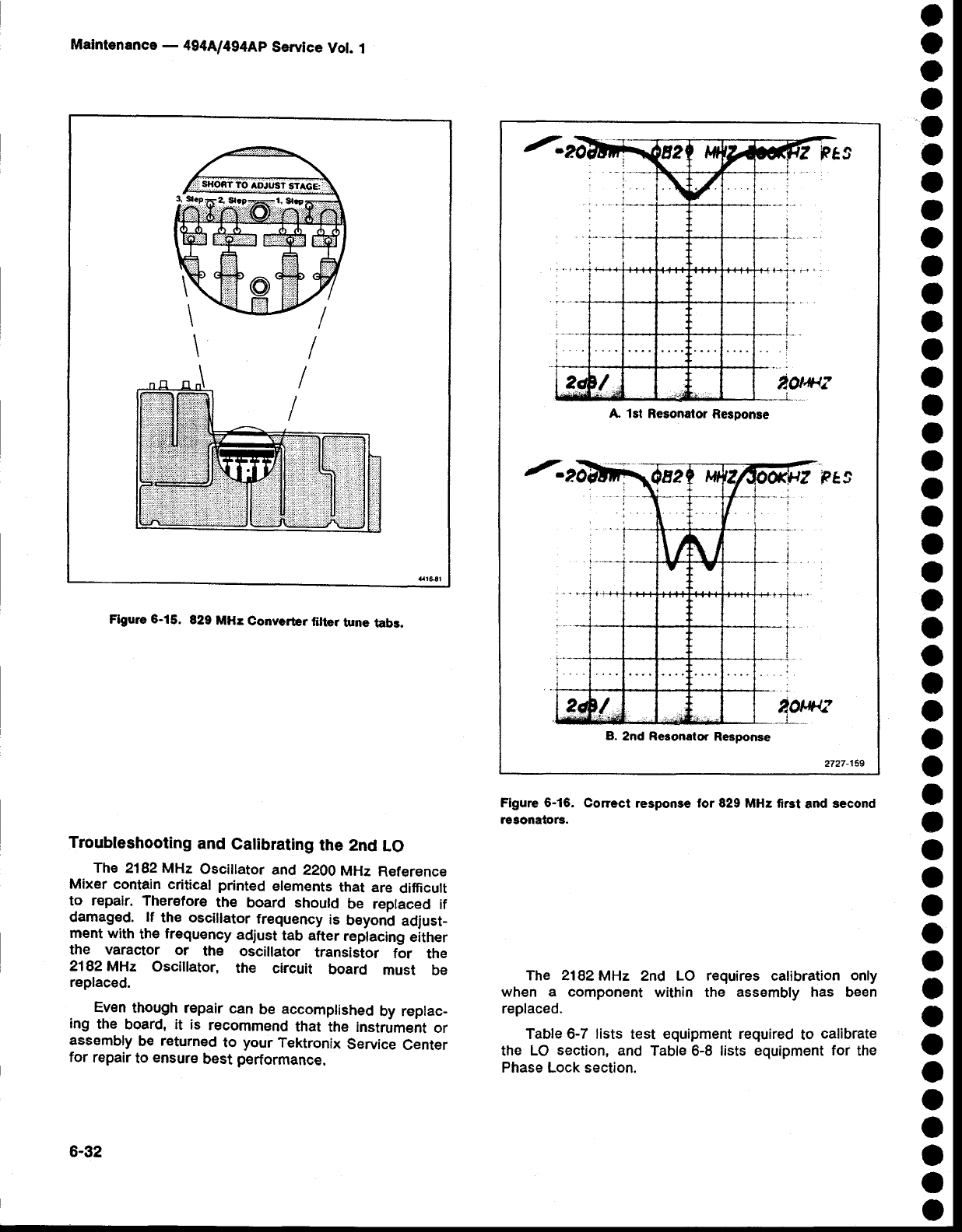
Malntenance
- 494A/4g4Ap
Service
Vol. 1
Flgure 6-'15. 829 MH: Converbr lilte. hlne tabs.
Troubleshooting and Calibrating the 2nd LO
The 2182 MHz Oscillator
and 2200
MHz Reference
Mixer
contain
critical
printed
elements
that are difficult
to repair. Therefore the board should be replaced if
damaged. lf the oscillator frequency
is beyond
adjust_
ment
with
the
frequ€ncy
adjust
tab
after
replacing
either
the varactor or the oscillator transistor for the
2182
MHz Oscillator, the circuit board must be
replaced.
Even
though repair
can be accomplished
by replac-
ing the board, it is recommend
that the instrument
or
assembly
be returnEd
to your
Tektronix
Service
Center
for repair
to ensure
best
performance.
Figure 6-16. Correct responee for 829 MHz
first and second
resonators.
The 2182MHz 2nd LO requires calibration
only
when a component
within the assembly has been
replaced.
Table 6-7 lists test equipment required
to calibrate
the LO section,
and Table 6-8 lists equipment
for the
Phase Lock section.
o
o
o
o
o
o
a
o
o
O
o
o
o
a
o
o
I
o
a
o
o
o
o
o
a
o
o
o
o
o
o
o
o
o
o
t
o
o
o
o
o
O
o
o
A. lsl Resonalor
Response
B. 2nd Regonator Response
Fe5
2727-159
6-42
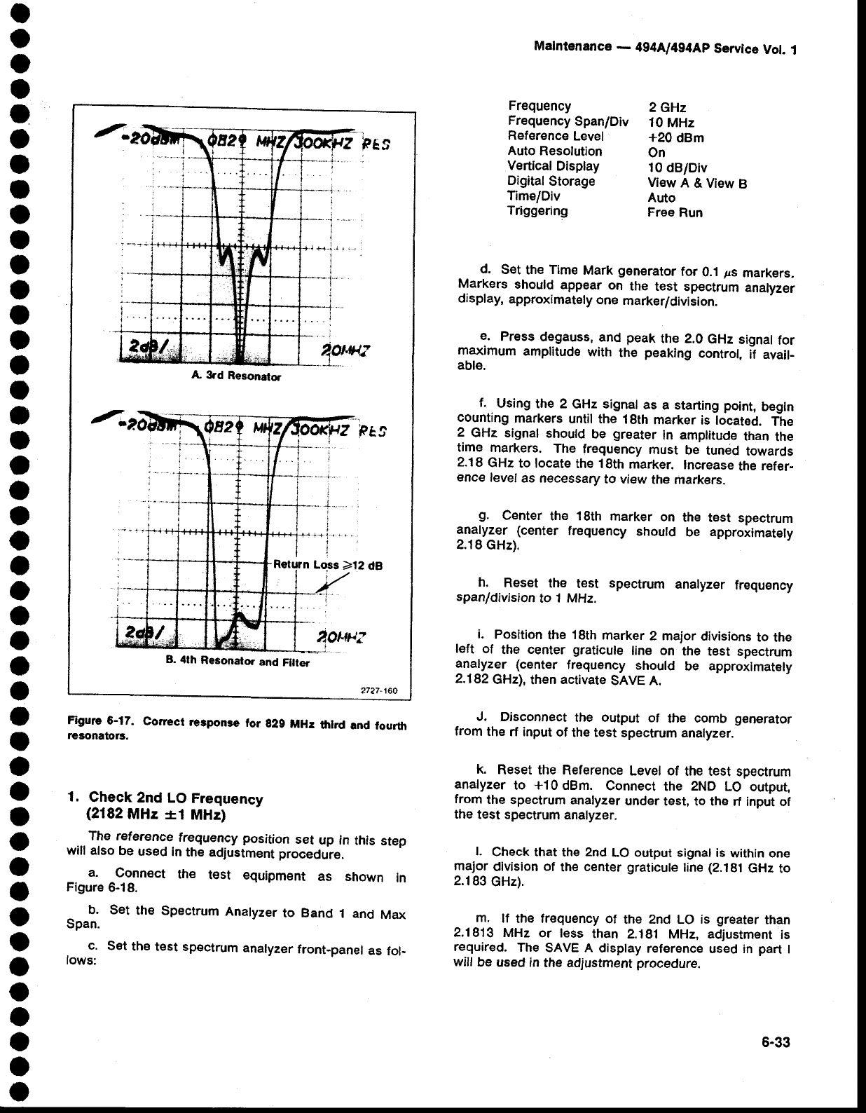
o
O
o
I
a
o
o
I
O
o
o
t
o
I
o
I
I
I
o
o
O
o
a
O
o
O
a
O
o
o
a
o
o
o
O
o
o
o
o
o
o
a
o
o
Malntenance
- 4g4A/4g4Ap
service
vot. 1
A 3rd Resonator
Retu?n
Lo-ss
>12 dA
B. 4th Resonator and Fllter
Figure
6-17. Corect re3ponse
tor g29 MHr tlrlrd and fourth
resonators.
d. Set
the
Time
Mark
generator
for 0.1
Fs
markers.
Markers
should
appear
on the test sp€ctrum
analyzer
display,
approximately
one
marker/division.
e. Press
degauss,
and peak
the 2.0
GHz
signal
for
maximum
amplitude
with the peaking
control,
if avail-
able.
f. Using
the 2 GHz signal
as a starting
point,
begln
counting
markers
until the 18th
marker
is located.
The
2 GHz signal
should
be greater
in amptitude
than
the
time markers. The frequency
must be tuned
towards
2.18
GHz
to locate
the 18th
marker.
Increase
the
refer-
ence
level
as necessary
to view
the markers.
S. Center
the 18th marker on the test spectrum
analyzer
(center frequency
should be approximately
2.18
GHz).
h. Reset the test spectrum analyzer
frequency
span/division
to 1 MHz.
i. Position
the 18th
marker
2 major
divisions
to the
left of the center graticule
line on the test spectrum
analyzer
(center frequency
should be approximately
2.182
GHz),
then
activate
SAVE A.
J. Disconnect
the output of the comb generator
from
the
rf input
of the test
spectrum analyzer.
k. Reset the Reference
Level of the test spectrum
analyzer
to +10 dBm. Connect
the 2ND LO output,
from
the
spectrum analyzer
under
test, to the
rf input of
the
test spectrum
analyzer.
l. Check that
the 2nd
LO output signal
is within one
major
division
of the
center graticule
line
(2.181
GHz
to
2.183
GHz).
m. lf the frequency
of the znd Lo is greater
than
2.1813
MHz or less
than 2.181
MHz,
adjustment
is
required.
The
SAVE A display
reference
used in part
I
will
be
used in
the adjustment
procedure.
Frequency
Frequency
Span/Div
Reference
Level
Auto
Resolution
Vertical
Display
Digital
Storage
TimelDiv
Triggering
2GHz
10
MHz
+20 dBm
On
10
dB/Div
ViewA&ViewB
Auto
Free
Run
1. Check 2nd LO Frequency
(2182
MHz *i MHz)
...
The reference
frequency
position
set up in this
step
will also
be
used
in
the
adiustrnent
procedure.
a. Connect the test equipment as shown in
Figure
6-18.
Set the Spectrum Analyzer to Band 1 and Max
Set the test spectrum analyzer
front-panel as fol-
b.
Span.
c,
lows:
6-33
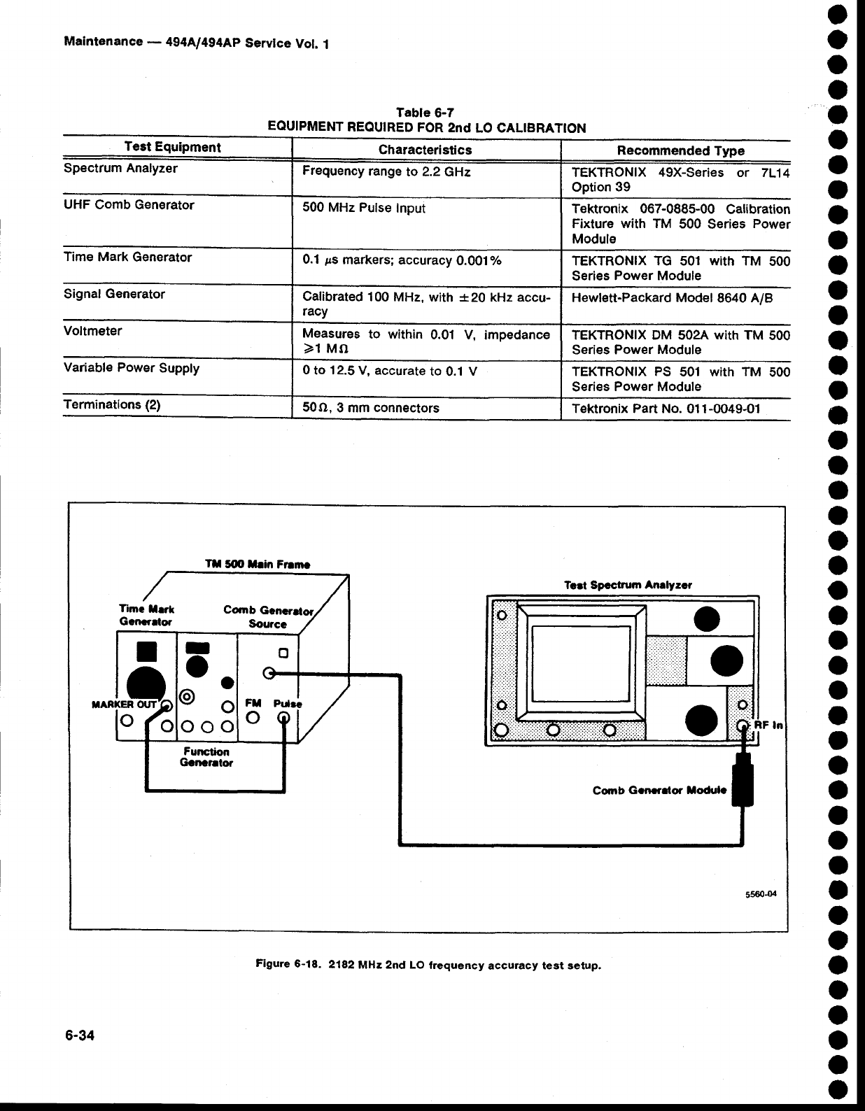
o
o
o
a
o
o
o
o
o
o
o
o
O
o
o
o
I
o
o
o
o
o
o
o
o
o
o
o
o
o
O
o
o
o
o
o
o
o
o
o
o
a
o
o
Maintenance - 494A/494Ap Servlce Vol. 1
Table 6-7
EQUIPMENT
REOUIRED
FOR
2nd LO CALTBRATTON
Test
Equipment Characteristics Recommended
Type
Spectrum Analyzer Frequency
range
to 2.2 GHz TEKTRONIX
49X-Series
or 7L'14
Option
39
UHF
Gomb Generator 500 MHz
Pulse
Input Tektronix 067-0885-00 Calibration
Fixture with TM 500 Series
Power
Module
Time Mark
Generator 0.1
,rs
markers; accuracy
0.001o/o TEKTRONIX TG 501 with TM 500
Series
Power Module
Signal Generator Calibrated
100 MHz.
with +20 kHz
accu-
racy Hewlett-Packard Model 8640 A/B
Voltmeter Measures
to within 0.01 V, impedance
>1
MO TEKTRONIX DM 502A
with
TM 500
Series Power
Module
Variable Power
Supply 0
to
12.5
V, accurate
to
0.1
VTEKTRONIX PS 501 with TM 500
Series
Power Module
Terminations (2) 50O,
3 mm
connectors T€ktronix
Part
No. 011-0049-01
Tt 5@ X.an Fr.m.
Tcrt Spcclnrm An.lyrct
Timc
trrt
Gcnetrlor Comb
Gcnc
Sourcc
Coorb Goneclor lodrlc
5560-{X
6-34
Figure 6-18. 2182
MHz 2nd LO frequency accuracy test setup.

o
o
o
a
I
o
o
I
O
o
o
O
O
o
I
o
a
I
a
a
o
o
a
o
o
I
o
O
I
o
a
O
I
o
a
a
o
o
O
o
o
o
o
o
Preparing the 2nd LO Assembly lor Adjustment
.. T_":!
_"guipment
setup
is shown
in
Figure
6-19. Turn
the POWER
off. Rernove
the cabinet
and place the
Spectrum
Analyzer_upside
Oown
io-ine nf Oect<
is
exposed. Use a 5/16 inch wrench to loosen and
remove
the two semi-rigid
cable connections
to the
assembly.
Remove
the flexible
coaxial
cable
connec_
tion
to
the't00
MHz
input.
Remove
the 14 screws that hotd the cover on the
mu-metaf section
and remov€
the cover. Unsolder
the
feads to feedthrough capacitors CZidS and CZ2O4.
fl'hese are the center two feedthrougfr
lerminals that
feed
through
the
circuit
board,
as
strovin
in'figure
O-iOj
Replace
the
cover
using
two or
three
screws
to hotd
the cover
in
place.
Remove the mounting screws for the 2nd LO
131e1OtV.
Carefuly
tift the 2ncr
LO assembty
from tnl
chassis
and turn it over so the machin€d
aluminum
housing
is up. Be sule that the pawer
input
"onn""-
tions remain
intact. place the ars"ruty on a flat sur-
I"9:: U1e
a 5/64 Ailen
wrench
to remove
the screws
holding
the
lid on the machined
atuminum
housing,
and
r".T9ug.
the tad,
exposing
the three
RF circuit boards
within
the osciffator
section.
Install
a 50O terminator
on the
21g2
MHz buffEred
output port,
p222,
(see
Figure
6_21).
2. Adjust 2nd LO Frequency
(2182 MHz *t MHz)
a. Connect the test equipment
as shown in
Figure
6-19.
b. Set the variable pow€r
supply
to 0 V. Connect
the
plus
posifive
(+)
terminat
to ttri'enO
LO housing
and
the.
ne-gative
(-) terminal
to the exposeO
Lno ot CZ2OI
and
L2031,
through
a 1 kO resistor.
c. Appty
a 100
MHz,
0_dBm
signal
from the signat
generator
to the 100
MHz Referenie
input port, p221.
(Frequency
must
be
within
20
kHz
of 10O
MHi.)
d. Connect
the test spectrum
analyzer
to the 21g2
MHz.
unbuffered
output port, p220. tni" is the test
spectrum
analyzer
with the reference
frequency
position
lr.fry- :gllp in step
1. Do
Nor
posinou
exy op
THE
CABLES
OVER
THE
2ND
LO
ASSEMBLY
OSCIL-
LATOR
SECTION
BECAUSE
THEY
CAN
AFFECT
THE
FREQUENCY
OF
THE
OSCILLATOR.
e. Bend
the
feedback
and
frequency
adjusting
tabs,
C1021 and C1922 (C and
D in Figure
O'-Ztiso
they
are
approximately
30 degrees
above
the board
surface.
- f. Apply power
to both
the Spectrum
Analyzer
and
the variable power supply. Set the voltage
output from
the variabte
powsr supply
to 5.0
V. Votiige on C2203
should
now
equal,
-S V and
a signal
strout-tO
appear
on
the
test spectrum
analyzer.
Maintenance
_ 4g4[l494Ap Servtce
Vot.
1
g. Check
for a voltage
of *10.0 V, r0.7 V across
c2023.
h. Check
Vbe
at Tplols (B in Figure
6-21).
tf Vbe
ls greater
than +0.9
V, push
the feeaback
adjustment
tab down
stightly
and
it tess
than
_0.9
V, tift
tha
tab. lf
Vbe
is greater
than
+O.g
V, replace
the microstrip
oscil-
lator
board. lf Vbe
is more negative
than
_1 V, check
th:9T circuitry. Adjust
tne iaO so Vbe is +0.15V,
t0.O5V at Tplois. Do not touch the feedback
tab
whilE
measuring
voltages.
i, Check
that the
2nd
LO
signal
(frequency)
is
within
9j'9- major division of the center Sratiiute tine
(2.181
GHz
to 2.18it
cHz). B,end
the freq-uency
adjust_
ment
tab c1022 (D In Figure
6_21)
to bring
the oscitiator
within tolerance. (Bend
the tab up tt increase
fre_
quency
and
down
to lower
frequency.)
j. lf unable
to bring
the oscillator
frequency
within
rry-e with the adjustment
tab, the frequency
of the
2182
MHz osciilator
can be brought
within range
of the
adiustmen-t
tab
by short€ning
a transmission
line stub (A
in Figure
6-21). Graduation
marks
along
the
side
of
the
stub provide
a guide
to calculate
trequency
corr€ction.
Each
minor
mark
from the end or cui across
the stub,
represents
an approximate
change
of 25
MHz.
k. Check
the frequency
by noting
the
t€st spectrum
analyzer
disptay. tf the
frequency
is too high,
ihe stub
must be lengthened
by soldering
a bridge
across
th€
cut. Recheck
the freguency. lf the frequency
is too
low,
the
stub
must
be shortened
l. Shorten the line so the frequency
is near
2200
MHz. For example: The freguency difference
between
the desired
and
tho actual
divideO
Oy eS
UH.,
equals
the number
of minor
divisions
from
the line
end
for the new
cut. Make
a cut across
thE line
and
check
that the new frequency
is near
2200
MHz. Repeat
as
necessary,
the use the adjustment
tab to bring the
oscillator
within
tolerance.
m. Check
2182MHz
output
pow€r.
Before making power measurements,
ensure
that the unused
port is t€rminated
into 50O. Unterminated ports
will degrade
both frequency
and
power
measurements.
(1) Check for 0 dBm +3 dB output power
at the
unbuffered
port, P220.
(2) Connect
the
test
spectrum
analyzer
to p222,
ter-
minate
P22O
in 50e, then
check
for an output
level
of +10 dBm *3 dB from
the
bufiered
port.
6-35

Maintenance
- 494A/4g4Ap
Servtce
Vot.
1
2lE2 }'/Hz tro||! Unbuttcrcd OrIput Porf
ffiffi
o@@@
@ 9o
Flgure 5-19. 2182 MHz Phase Locked 2nd LO adiustment letup.
t
o
a
I
o
o
o
o
o
a
o
a
o
a
o
o
I
I
o
o
I
a
a
o
o
o
I
o
o
t
a
t
I
a
I
t
o
o
o
I
o
o
t
I
Maintenance
- 4g4Al494Ap
Service
Vot.
1
c2201
TP
+12
V
ol ?o,il,-
.e:
,- zrfP2o3s-+o 5
r (2)--
r _rr r1l*rffi
Figure
6'20. 16-20 MHz
phase
Lock circuit test point
and
component
rocadons.
H222
21E2
tH: Bullercd Output port
2182 llHz MGrorlrip Olcitfatof
?zm Pi221
21E2
tHz t ntutfored Ou$ut port l(Xt lrHr ieErance fnpuf
0 d8m
2i200$HzReferencetircr XX$ElzRelersncs
Dlffercncc Frcqcncy
supplicr 2782ffi12 Tune
lnPut
A :Centcr trequoncy
tunang
!fub
9 :Bets,emitter voltage
telednt Tp1O15
C :Fcedback rdiu3lmcnt
teb
CtO2l
O -Ccnter trequency
edjurtrnent t b C1022
o F, qfo-
w
)LH-3
Flgure 6-21. 2182 MHz 2nd LO adiustment and test point tocations.

Mafnfenance
- 4g4Ll494Ap
Servtce
Vot.
1
Figure
6-22. Coaxial
test probe
construction
detaits.
3. Gheck the 2200 MHz Relerence Mixer
a. Use a probe, consisting
of a short length
of
semi-rigid
coaxial
cabte
with a dc block (see
Figure
6_
22), to connect the output of the reference mixer at
Q2204-to the input of the test spectrum analyzer.
Ground
the outer
shield
of the
coaxial
cable
againsi
the
2nd
LO housing.
b. Conftrm that the output signal frequency
is
18
MHz *1 MHz. Adjust the tab C1022
6ilure O_et1
for the 2182MHz
Microstrip
Osciilator,
to Lring
the 1ti
MHz
within
the
1 MHz
tolerance.
c. Confirm
that
th€ output
level
of the 1g
MHz
sig_
nal is approxirnately
-36 dBm. lf the level is below
-46 dBm, check the signat
levets
from the 2200
MHz
Reference
Mixer and the 2192
MHz Microstrip
oscilla-
tor (-28 dBm, *8 dB from the 22OO
MHz Reference
Mixer
and
+8 dBm,
*g dB from
the oscillator).
d. check
the 2192
MHz
tune range
(1) Vary the vottage
to the 21g2MHz tune line
between
0 V and -12.5 V and note the fr€quency
change at c22a4
(the
output
of
the
22oo
MHz
Refei_
ence
Mixer).
(2) The frequency
should
vary
between
20
MHz and
35 MHz as the tune line
voltage
is varied
between
0 V and
-12.5
V.
Reassembling the 2nd LO Assembly
1. Disconnect
and
remov€
the
connections from
the
variable
power
supply
and the
test
spectrum
analyzer,
2. Replace
the lid for the oscillator
housing
and
install
the 26 screws. Install the screws
loosely,
then
tighten
them starting
from
the
center
of the lid and
pro-
gress
along
the
edges
toward the
corners
to insure
that
no gaps exist between
the lid and the housing, Any
gaps will allow
RF leakage
that can produce
spurious
respons€s.
3. Reinstall
the assembly
on the RF
deck.
Remove
the 50O terminatlons and reconnect
the
cables. Use
a
5116 inch open-end
wrench to tighten
the semi-rigid
coaxial connectors
to 8 to 10 lnch-pounds.
4. Remove
the mu-metal lid and reconnect the
feads
to feedthrough
capacitors C22Og
and C2204,
on
the Phase Lock board (Figure
6-20). Replace the lid
and
install
the 14 screws. Tighten
the screws
from
the
center
toward the corners of the lid to prevent
gaps
between
the lid and the housing. Do not overtighten
because the screws are
easily stripped.
O
a
o
a
a
o
a
o
o
o
I
a
o
a
a
,
o
a
I
o
o
o
o
o
o
I
o
o
o
t
O
o
o
o
I
o
o
o
o
o
o
O
O
o
trc BLOC|(
\_r
CASLE ASSETBLY
6-38
6-39
o
O
o
a
O
o
O
t
o
I
o
I
o
I
I
t
o
I
a
a
o
a
a
o
o
a
o
o
I
I
a
a
I
O
o
a
o
o
a
o
a
o
o
I
Maintenance
_ 494A/494Ap
Service
Vot.
1
Tabte
6-g
EOUIPMET.IT
REOUTRED
FOR
CALTBRATING
THE
16-20]VtHz
pHASE
LOCK
C|RCU|T
Tesl fqulprng6l Characteristlcs Recommended Type
utgtrat v9tlmeter
Frequency
Counter
Time-Mark
Generator
Measures
to within 0.Ol V, impedance
>1Mo TEKTRONTX
TM S00-series
DM
501A,
DM
502A, or
DM
SO10
Frequency
to g0
MHz TEKTRONIX TM SO0-Series DC
503A,
DC
508A,
DC
509
y1ll9l output,
1 s to 1 ps; accuracy
0.001o/" TEKTRONIX
TG
501
servtce Kit Extend€r
Board Tektronix
Part No. 622-0g65-00
CENTER
FREOUENCY
CONTROL
SOARD
Oil EXTENDER
DIGITAL
VOLT
METER
TITE
OIGITAL TARX
COI'NTER GENERATOR
SPECTRUil ANALYZER
Flgure 6-23. 2182 MHr 2nd LO phase Lock adiu3tment setup.
Maintenance
- 494A/{g4Ap
Servtce
Vol. I
Troubleshooting and Galibrating the 16-20 MHz
Phase Lock Section
Replacing
oscillator
components
in this section
may
alter sweep
linearity
and the oscillator
frequency. Thi
following
checks
and calibration
aid in repairing
and
retuning
the assembly.
1. Preliminary
_ a. Test equipment
setup
is shown
in Figure
6-23.
Remove
and
install
the Center
Frequency
Control
board
on an extender
board.
b. Switch POWER
on and
set
the FREO
SPAN/D|V
to 1
MHz.
2. Check Voltages
- a. Check all input
voltages
at
the
feedthrough
capa_
cJtors
in the housing
wall. RefEr
to Figure
OZb
or ine
data printed
on the tid. The vottage
LEVEL
at the
sweep
and
tuns
input
lines
should
be 0 V +O.OS
V with
the
FREQ
SPAN/D|V
)500 kHz.
b. Switch
the POWER
off. Remove
the tid
frorn
the
mu-metal
housing
assembly
to gain
access
to internal
circuitry.
c. Switch
POWER
on,
then
check
the
internal
regu-
lated
voltages;
+12
V *0.4 V at C2201,
-12V *O.i V
at C2202, and +S.2
V *0.2S V at TplO109 (see
Figure
6-16).
Check
the
output
of the shaper
at
Tpl0gg
for a level
between
+0.9
V and
-0.3 V (0
V i0.g V).
3. Setting Center Frequency
a. Connect a frequency
counter
to Tp2O35
and
note
the frequency. tf the frequency
is within S0 kHz of
18
MHz no correction
is necessary; proceed
to part 4
(Setting
Tune Sensitivity
and nangay. tf outside
the
range
proceed
as
follows:
(1) Turn
POWER
off. Unsotder
and
remove
one end
of Shaper
Offset
resistor
R1070.
Unsolder
the wire
strap
between
T2092
and
T1091,
at the T1091
end.
and
lift
it free.
(2) Solder a flexible
wire
jumper
to the T2092
end;
then,
by means
of a a plastic
tuning
tool,
attach
the
free end to one of the three pads for T1091
and
note
the frequency
readout
of the counter.
ll this flexible wire touches ground whil€ the
circuit is operating, the supply regulators
can be damaged. The regulators are not
protected
against a short circuit.
(3) lf one of the pads provides
a frequency
that is
within
the range
of 17.5
MHz *0.2S MHz,
solder
the
wire strap to this pad. lf the frequ€ncy
is still out-
side the range,
movE the
jumper
to the other pad
for
T2092 and repeat the procedure. Frequency
must
equal
17.5
MHz +0.25
MHz.
b. Turn POWER
OFF. Replace
R1070 with a 10
turn
25 kO potentiometer
in series
with
a S ko resistor.
c. Turn POWER
on and
with the counter
connected
to TP2035, adjust th€ potentiometer
for a frequency
readout
of 18
MHz *50 kHz.
d. Turn POWER off, measure
the total resistance
valu6 and teplace R1070 with a lyo resistor
of thls
measured value. Switch
POWER
on and recheck
the
frequency to ensure that it is 18 MHz *50 kHz.
Disconnect
the
counter
from
TP2035.
4. Setting Tune Sensitivity and Range
a. Center
the Fine Tune adjustment
R4040,
on the
Center Frequency
Control
board
and
the
2nd LO
Sweep
adjustment Rl067, on the Span Attenuator board
(Figure
6-24).
b. Decrease
the FREQ
SPAN/D|V
to 200 kHz or
less. The 2nd
LO
is now in
the
center
of its
tune
range.
c. Press <Blue-SHIFT>
10
dB/DlV
to disabte
frs-
quency corrections. Press <Blue-SHIFT> PULSE
STRETCHER
and select item #0 (ALTERNATE
FRE-
QUENCY DfSPLAY),
then item #2 (znd LO FRE-
OUENCY DISPLAY).
Beadout will now indicate
the
2nd
LO
frequency.
d. Tune
the 2nd LO to one end of its range
where
the frequency readout
no longer changes. Note
the frE-
quency
and measure
the voltage
on the Tune
Line at
the input feed-through
capacitor
(Figure
6-20).
e. Tune
the 2nd LO to the other end of its range
and
again note
the frequency and
the
new
voltage
read-
ing.
f. Calculate
the frequency change
per vott (fre-
quency
range versus
voltage
range).
Frequency
change
per volt should equal 128.0 kHz *10o/o or range
between 115.2
kHz and 140.8 kHz.
g. lf the
frequency/volt change
is low, decrease
ihe
vafue of R2072
(Figure
6-20).
h. Press <BIue-SHIFT>
PULSE
STRETCHER
and
menu item #1. then select
the 2nd LO for calibration.
Perform
the procedure
that is called out for adjusting
the Fine Tune
Range R4040 and Fine
Tune Sensitivity
R3040
to calibrate
the
2nd LO
tuning range.
o
o
o
O
)
a
o
a
o
t
o
o
o
a
a
o
a
o
o
o
o
o
O
o
o
o
t
o
o
,
o
O
o
o
o
t
o
o
o
O
o
o
I
o
6-40

o
o
o
a
o
o
o
o
o
o
o
o
o
o
I
o
o
o
a
a
o
a
o
o
I
o
a
a
I
I
I
a
I
o
o
a
t
o
o
o
o
a
o
o
Maintenanco
- 4g4A/4g4Ap
Servlce
Vol.
1
Figure 6-24, Tune and Sweep Range adjustnents.
R404O
Fine
Tune
Ranee
-+!
CENTER
F
REOUE'{CY
COI{TROL
A. Location of R4040, Fine tune Renge.
)
B. Location ot R|O6Z.2nd LO Sweep.
Maintenance
- 494A/4g4Ap
Servlce
Vot.
1
5. Setting Sweep Range
a. Apply
5 ps time markers
from the Time
Mark
Generator
to the
RF tNpUT.
Set
the FREO
SPAN/D|V
to 500 kHz then back to 200 kHz to center
the 2nd LO
frequency.
b. Adjust the REF LEVEL to disptay
the 200
kHz
markers then center one of the markers with the
CENTER FREOUENCY
controt.
c. Adjust
the 2nd LO Sweep
R1O6Z,
on the Span
Attenuator
board (Figure
6241,
so the comb lines on
opposite
sides
of the screen,
are exactly
g major
divi_
sions
apart.
6. Check and Adjust Tune Linearity
a. With Frequency
Corrections
disabled
(see part
2), apply 5 ps markers
from a Time Mark Generator
to
thE
RF INPUT.
SEt thE FREQUENCY
tO 20
MHZ.
FREQ
SPAN/DIV
to 200
kHz and activate
AUTO RESOLN.
Adjust
th€ REF
LEVEL
so a comb
of 200
kHz markers
is
displayed.
b. Turn
the
CENTER
FREQUENCY
controt
count€r-
clockwise until the c€nter frequency
stops tuning,
decrease FREQ SPAN/D|V
to 50
kHz then tune tfre
CENTER FREQUENCY
up untit a marker
signal
is one
major division
from the left edge of the graticule. A
comb line
(or marker
signal)
should
appear
on or near
the first major division
in from the right sid€ of th€
scr€en.
c. lt the right marker is not exacily
g divisions
from
the left marker,
note
the €rror
to th€ nearest
0.5 minor
division.
d. Tum the CENTER
FREQUENCY
control ctock-
wise, to increase center frequency,
until the next
marker signal
is one divislon
in from
the lett edge and
again note thE spacing between
this marker and the
marker
near
the right
edge.
e. Continue
this process
of tuning
up in frequency
until the
center
frequency
stops
tuning, noting
the slgnil
spacing
at each
check
point.
f. lf the peak-to-peak
enor is 2.5 minor
divisions
(25
kHz) or l€ss,
the lin€arity
over
the center
2 MHz of
swEep is satisfactory;
if more,
the shaper
needs
adjust-
ment or repair.
g. Switch
the FREQ
SPAN/D|V
to 200
kHz,
tune to
the low end of the sweep
range
and note
the linearity
over the center
eight
divisions
of span,
then
tune to the
high
end
of the 2nd
LO range
and
again
note
the
linear-
ity. Peak-to-peak
deviation should not exceed 0.5
minor division.
h. lf the
shaper
needs
adjustm€nt
or
repair proceed
as follows:
o
o
o
o
o
o
o
t
o
a
o
t
o
O
o
I
o
o
o
a
a
o
o
o
a
o
a
o
o
t
t
o
o
o
o
a
t
o
a
o
o
a
o
a
6-42
(1) A shaper
diode or resistor
may be defective
if
the comb
line spacing
is consistent
for part of the
tuning range and 30 kHz or tnore off for the other
parts of the sweep. To test the diodes
for forward
conduction,
tune to the low end of the range and
short R2049
(Figure
6-20). The output of U1073A
(pin 1) should
equal
about
*3V. Ut0S9 diodes
B
through
G and U2059
diodes
A through
F should
ail
have
a 0.48 V forward drop. Use
a floating
or digital
voltmeter
to check the drop.
(21 Tum POWER off then temporarily replace
Shaper
resistor
R2049 with a 20 kO potentiometer.
Switch POWER on, and adjust the potentiometer
to
obtain the best overall linearity; decreasing
resls-
tance will decrease the spacing between
comb
lines
in the upper portion of the tune range and spread
the spacing
for the lower portion. Increasing
the
resistance
of R2049 will reverse
the effect. When
the correct setting is found,
turn POWER
off, meas-
ure
the resistance,
and replace with a fixed
resistor
of
the same or near the same
value.
i. Check the
tun€
sensitivity
and sweep
range
of the
2nd LO. Repeat
steps 4, 5,
and
6 if necessary.
7. Conclusion
a. Replace
the
housing
lid with its 14 screws.
b. Tighten
the screws
sequentially,
starting
from
the
center of the lid and
progressing
toward the
corners
to
prevent
gaps between the lid and the housing. Use
care
to not strip the screws as you
tighten
them.
c. This completes
the 2182 MHz
Phase
Locked 2nd
LO
calibration.
Refer to "Adjust
control
system" in Sec-
tion
5 for readjusting the system.
Troubleshooting Aids for the 2182 MHz Phase
Locked 2nd LO Assembly
lf the Phase Locked assembly
is in the
instrurnent,
set the FREQ
sPAN/Dlv to 500
kHz
or more so the 2nd
LO
is not sweot.
The difference frequency signal
(18
MHz) from the
2200 MHz Reference Mixer is amplified and fed to
P224. Nominally,
its amplitude
is -5 dBm into 50O.
P224 is convenient
for monitoring the 16-20 MHz
VCO. When
phase
lock
is operating, the difference
fre-
quency
exactly equals the frequency
of the vco. lf
phase
lock is not functioning
properly,
the difference
frequency signal will either disappear
completely
or
tune
to its range
limit
of -6 MHz or 30 MHz.
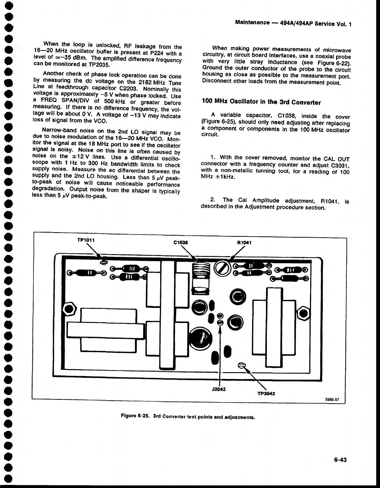
o
o
o
o
o
o
o
I
o
o
o
o
o
I
I
I
I
o
a
o
t
a
o
o
o
o
o
a
o
I
I
o
I
o
o
O
o
I
a
o
o
a
o
o
_ ^ wIT the foop is unlocked,
RF teakage
from the
16-20 MHz
osciilator
buffer
is present
.ip224 with
a
level
of --35 dBm. The-amplified
Omeience
frequency
can
be monitored
at Tp20gS.
Another
check of phase
lock operation
can be done
by measuring
the dc voltage on the 21g2
MHz Tune
Line at.feedthrough
capaciior C22Og.-ttominally
itris
voltage
is approximately
-5 V when phase
lock€d. Use
a FREQ SPAN/D|V of S00
kHz or greater before
measuring. lf there is no difference
freq-uency,
the vol-
tage
wilt
be about
0 V.-
l vottage
of _13
V may
indicate
loss
of signal
from
the
VCO.
Narrow-band
noise on the 2nd LO signal
may be
due
to noise
modulation
of ths 16_20 MiivCO. trton_
itor
the stgnat
at the tg MHz port
to """ ii ttre
oscittator
signal is noisy. Noise on this line is often caused by
noise on the *12V lines. Use a differentiat
oscillo_
scope
with 1 Hz to 300 Hz bandwidth
limits
to check
supply
noise. Measure
the ac Oifferentiat
Letween
the
supply
and
the 2nd LO housing.
Less
than
5 pV
peak-
to-peak of noise will cause noticeable performance
jeOradatign.
Output
noise
from
the shapel
is typicaily
less
than
5
pV
peak-to-peak.
Maintenance
_ 4g4N4g4Ap
service vot. I
. When making power m€asurem€nts
of microwave
circuitry,
at circuit
board
interfaces,
use a coaxial
probe
with v9ry litfle stray. inductance (see figure'O-ee1
Ground
the outer conductor of the pioUe
tolhe circuit
housing
as close
as possible
to the measurement
port.
Disconnect
other
loads
from
ths meaEurement
point.
100 MHz Oscillator in the 3rd Converter
A variable capacitor, C10gg, inside the cover
(Figure
6-25), should
only need actjusting
after reptacing
a.
component
or components
in the 100
MHz oscillatoi
circuit.
1. Wth the cover
removed,
monitor
the CAL OUT
connector
with a frequency
counter and adiust Cgoiil
,
with a non-metallic
tunning
tool, for a reading
of 100
MHz
rlkHz.
2. The Cat Amplitude adjustment,
Rl041, is
described
in the
Adjustment procedure
section.
1?8
TPttt4!
Flgure 6-25- 3rd Converter test poinb and adjustments.
6-43
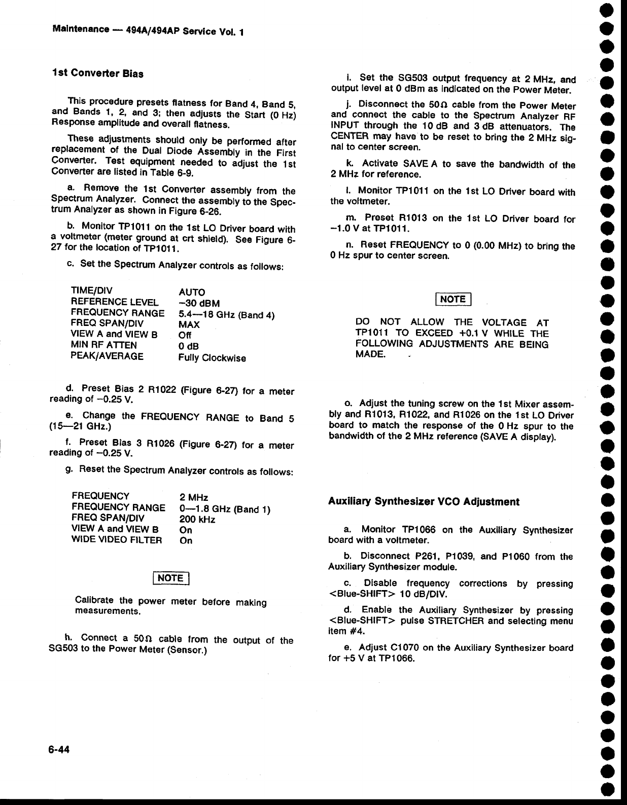
Malntenance
- 4g4A/4g4Ap
Servlce
Vol.
i
1st Converter
Bias
This
procedure
presets
flatness
for Band
4, Band
5,
and Bands
'1,
2, and 3,: then adjusts
the Start
(O
Hzi
Response
amplitude
and
overall
flatness.
These adjustments
should only be performed
after
replacem€nt
of the Dual Diode
Assem'bly
in the First
Converter.
Test equipment
needed
to adjust
the 1st
Converter
are
listed
in
Table
6-9.
a. Remove
the lst Converter
assembly
from the
Speetrum
Analyzer.
Connect
the assembly
t6 the Spec-
trum Analyzer
as
shown
in
Figure
G26.
b. Monitor
Tp1011
on the lst LO Driver
board
with
a_voltmeter (meter
ground
at crt shield). See Figure
6_
27
tor the
location
of
Tpl01
1.
c. Set
the
Spectrum
Analyzer
controls
as
follows:
i. Set the SG503 output
frequency
at 2 MHz,
and
output level
at 0 dBm
as indicated
on
the
power
Meter.
j. Disconnect
th€ 50O cable
from
the power
Meter
and connect
the cable to the Spectrum
Analyzer
RF
INPUT
through
the 10dB and
gdB attenuators.
The
CENTER may have
to be reset
to bring
the 2 MHz
sig-
nal
to center
screen.
k Activate SAVE A to save the bandwidth
of the
2 MHz for reference.
l. Monitor
TP1011
on the lst LO Driver
board
with
the
voltmeter.
m. Preset R1013
on the 1st LO DrivEr
board for
-1.0
V at
TP1011.
n. Reset
FREQUENCY
to 0 (0.00
MHz)
to bring
the
0 Hz
spur
to center
screen.
t
a
o
t
o
O
o
o
o
o
o
I
o
a
t
I
o
o
o
t
t
o
o
a
t
I
a
a
a
t
I
a
o
o
t
o
o
a
o
o
o
I
o
a
TIME/DtV
REFERENCE
LEVEL
FREQUENCY
RANGE
FREO
SPAN/D|V
VIEW
A and
VIEW
B
MIN
RF
ATTEN
PEAK/AVERAGE
AUTO
-30 dBM
5.4-18 GHz
(Band
4)
MAX
ofi
0dB
Fully
Glockwise
DO NOT ALLOW THE VOLTAGE AT
TPlOll TO EXCEED
+0.1
V WHILE
THE
FOLLOWING
ADJUSTMENTS
ARE BEING
MADE.
o. Adjust
the
tuning screw on
the 1st Mixer
assem-
bfy
and
R1013,
R1022,
and
Rl026 on
the 1st LO
Driver
board to match the response
of the 0 Hz spur to the
bandwidth of the 2 MHz reterence
(SAVE
A disptay).
Auxiliary Synthesizer VCO Adjustment
a. Monitor TP1066
on the Auxitiary
Synthesizer
board
with a voltmeter.
b. Disconnect
P261, P1039, and p1060 from the
Auxiliary
Synthesizer
module.
c. Disable frequency corrections by pressing
<Blue-SHIFT>
1
0 dB/DlV.
d. Enable the Auxiliary Synthesizer
by pressing
<Blue-SHIFT>
pulse
STRETCHER
and
selecting
menu
item
#4.
e. Adjust
Cl070 on the
Auxiliary Synthesizer board
for +5 V at TPl066.
d. Preset Bias 2 R1022
(Figure 6-271
tor a meter
reading of -0.25 V.
e. Change
the FREQUENCY
RANGE
to Band s
(15-21 GHz.)
f. Preset
Blas 3 R1026
(Figure
6_27)
for a meter
reading
of -0.25 V.
g. Reset
the
Spectrum
Analyzer
controls
as follows:
FREQUENCY 2MHz
FREOUENCY
RANGE 0-1.9 GHz
(Band
t)
FREO
SPAN/D|V 200
kHz
VIEW
A and
MEW
B On
WIDE
VIDEO
FILTEH on
Calibrate
the power meter before making
measurements.
h. Connect a 50O cable from the output of the
SG503
to the Power
Meter
(Sensor.)
6-44
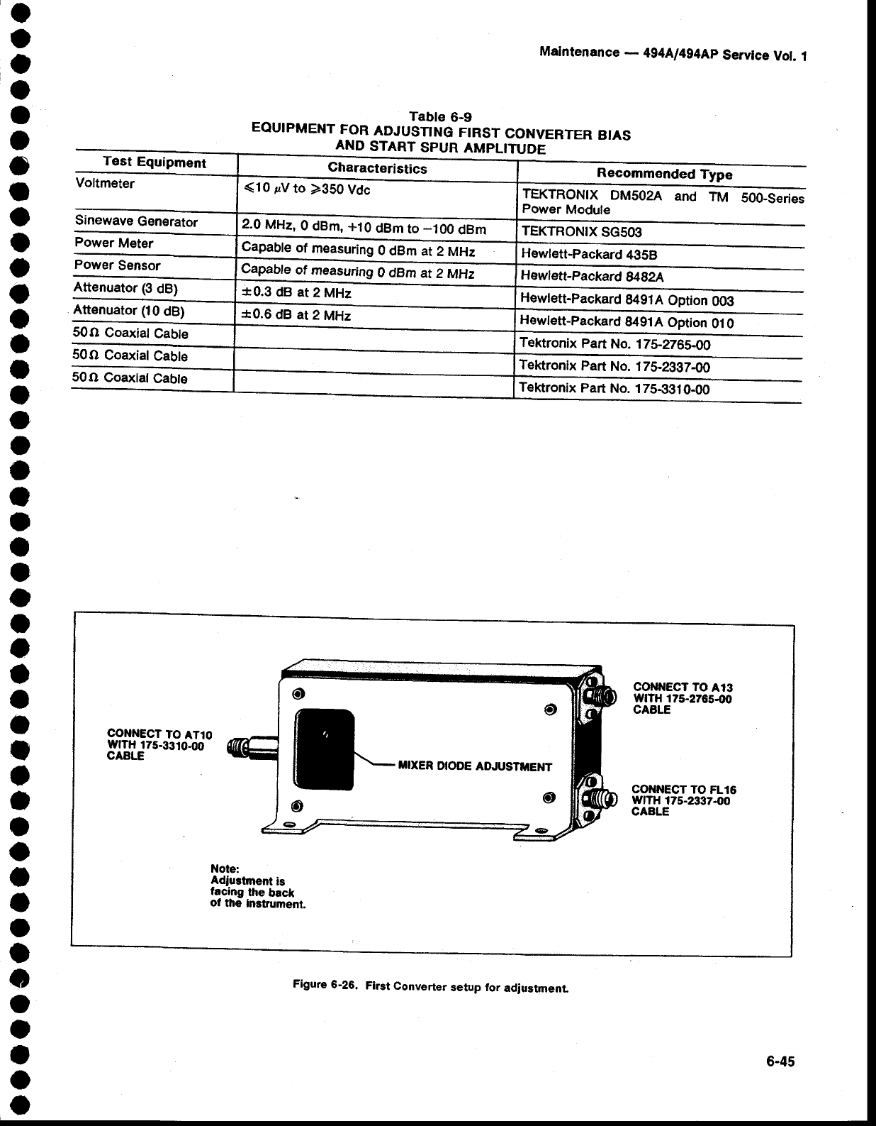
Malntenance
- 494A1494Ap
Servtce
Vol. 1
6-45
o
o
O
o
o
o
o
I
o
o
o
t
o
o
I
o
o
o
I
I
o
o
o
o
o
o
a
a
o
o
t
a
o
a
a
o
o
o
o
o
O
a
o
o
Table 6-9
EQUIPMENT FOR ADJUSTING FIRST CONVERTER BIAS
AND
START
SPUR
AMPLTTUDE
Test Equipment Characteristics Recommended Tvoe
vottm€ter
Sinewave
Gengrator
(10 pV
to )350 Vdc TEKTRONTX
DM502A and TM SO0_series
Power
Module
2.0
MHz,o
dBm,
+10
dBm
to
_100
dBm TEKTRONIX
SG5O3
Power
Meter
...-
Polrrer
Sensor
Attenuator
(3
dB)
Capable
of measuring
0 Ogm
it 2 t\,tt-tz Hewlett€ackard 4358
Capable
of measuring
0 dBm
at Z Unz Hewlett-Packard
8482A
*0.3 dB
at
2
MHz Hewlett-Packard
8491A
Option
003
H€wl€tt-Packard
8491A
Option
010
Tektronix
Part
No. 175-276$00
Attenuator
(10
dB) *0.6 dB at
2
MHz
50O
CoaxiatCabte
5U{}
CoaxiatCable
50O Coaxiat
Cabte Tektronix
Part No. 175-2ggT-W
Tektronix
Part
No.
17S€g1O-00
CONNECT
TO
A13
tvtTH 175-2765-d'
CABLE
CONNECT
TO
AT1O
wtTH
175-3310-d)
CAELE
CONNECT
TO
FL16
wfTH 17s-2337-fi'
CAELE
Nole:
Adiu3tnent is
facing the back
ot the instrumeni.
Figure 6-26. First Converter setup for adjustment
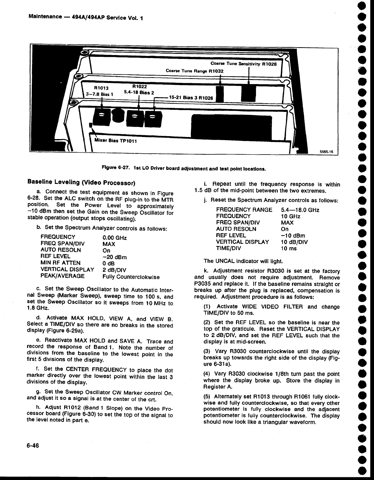
Maintenance - 4g4A/4g4Ap Servlce Vol. I
Flgure 5-27. 1st LO Ddyer board adjustment and test point locatlons.
o
o
o
o
o
a
o
t
o
o
o
o
o
o
I
t
o
o
o
I
o
o
o
o
o
o
a
a
o
t
t
I
o
o
o
O
o
o
)
o
o
I
o
o
Baseline Leveling (Video processor)
a. Connect
the test equipment
as shown
in Figure
6-28. Set
the
ALC switch
on
the
RF
ptug-in
to the
MTR
position. Set the power Levef to approximately
-10 dBm
thsn
set
the Gain
on the
Sweep
bscittator
foi
stable
operation
(output
stops
oscillating).
b. S€t
the
Spectrum
Analyzer
controls
as
follows:
FREOUENCY 0.00
GHz
FREQ
SPAN/D|V MAX
AUTO
RESOLN on
REF
LEVEL -20 dBm
MIN
RF ATTEN O
dB
VERT|CAL
DTSPLAY 2 dB/Dtv
PEAK/AVERAGE Fuily
Counterctokwise
c. Set
the Sweep
Oscillator
to the Automatic
Inter-
nal Sweep
(Marker
Sweep), sweep
time to 100 s, and
se! lhg Sweep
Oscillator
so it sweeps
from 10 MHz
to
1.8
GHz.
d. Activate
MAX HoLD, VIEW A, and VIEW B.
Select a TIME/DIV
so there
ar€
no breaks in the stored
display
(Figure
6-29a).
e. Reactivate
MAX HoLD and
SAVE
A. Trace
and
record
the response
of Band
1. Note the number
of
divisions
from the baseline
to the lowest
point in the
first
5 divisions
of the
disptay.
f. set the CENTER
FREQUENCY
to ptace
the dot
marker
directly
over the towest
point
within
the last o
divisions
of the
display.
-9. Set
the Sweep
Oscillator
CW
Marker
control
On,
ancl
adjust
it so
a signal
is at the cent€r
of the
crt.
h. Adjust
R1O12
(Band
1 Stope)
on the Video
pro-
cessor
board (Figure
6€0) to set
the
top of the
signalto
the level
noted
in part
e.
6-46
i. Repeat
until the frequency response
is within
1.5
dB of the mid-point
between
th€ h^/o extremes.
j. Reset
the Spectrum
Analyeer controls
as follows:
FREQUENCY
RANGE 5.4-18.0 GHz
FREQUENCY 10
GHz
FREQ
SPAN/DIV MAX
AUTO RESOLN ON
REF LEVEL -10 dBm
VERTTCAL
DTSPLAY 10 dB/DlV
TIME/DIV 10
ms
The
UNCAL indicator
will
light.
k. Adjustment
resistor
R3030 is set at the factory
and usually does not require adjustment. Remove
P3035 and
replace
it. lf the baseline
remains
straight
or
breaks
up after
the plug is replaced. compensation
is
required.
Adjustment
procedure
is
as follows:
(1) Activate wlDE vtDEo FTLTER
and change
TIME/DIV
to 50
ms.
(2) Set the REF
LEVEL so the basetine
is near
the
top of the graticule.
Reset
the
VERTICAL
DtspLAy
to 2 clB/Dlv, and set the REF LEVEL such
that the
display
is at mid-screen.
(3) Vary R3030 counterclockwise
until the display
breaks
up towards
the
right
side
of the display
(Fig-
ure
6-31a).
(4) Vary
R3030
clockwise
1/8th
tum past
the point
where the display
broke up. Store the display in
Register A.
(5) Alternately set
Rl013
through
Rl061 fully
clock-
wise and fully
counterclockwise,
so that every other
potentiometer
is fully clockwise and the adiacent
potentiometer
is fully
counterclockwise.
The
display
should
now look
like a
triangular waveform.
Coarse Tune Range R1032
3_Z.B
Etias
I 5.4-18.Bias
215-21
Bias 3 R1026
Mirer
Bias
Tptoll
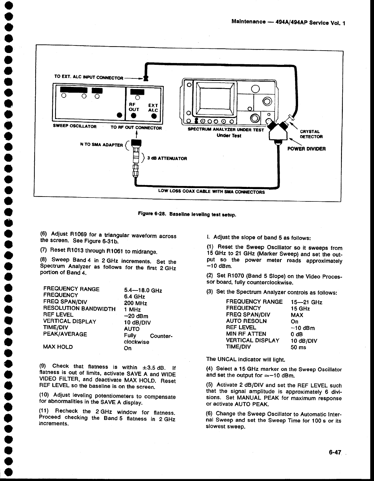
o
o
a
O
a
o
o
I
o
o
I
o
o
a
t
o
o
o
o
o
o
a
o
o
o
o
o
o
I
I
a
a
o
a
I
O
t
o
o
o
I
I
o
o
Figurc
6-28. Baseline
levefing
tert setup.
(6) Adjust R1069
for a triangular
waveform
across
the
screen.
See
Figure
6-g1b:
f/) Reset
Rl0tg through
Rl061 to midrange.
(8) Sweep Band
4 in 2 GHz increments.
Set the
Spectrum Analyzer as foltows for th€ first 2 GHz
portion
of Band
4.
l. Adjust
the
slop€
of band
5 as follows:
(1)
-Reset
the Sweep Oscillator
so it sweeps
from
15
GHz
to 21
GHz
(Marker
Sweepl
and
set
the out_
Plt 9o the power meter reads approximately
-10 dBm.
(2) Set R1070 (Band
5 Stope)
on
the Mdeo
proces-
sor
board,
fully
counterclockwise.
(3) Set
the Spectrum
Analyzer
controls
as
follows:
FREQUENCY
RANGE 15-2i GHz
FREQUENCY 15GHz
FREQ
SPAN/DIV MAX
AUTO
RESOLN On
REF
LEVEL -1OdBm
MIN
RF
ATTEN O dB
VERTICAL
DTSPLAY 10
dB/Dtv
TIMEID|V 50
ms
The
UNCAL
indicator
wiil
tight.
(4) Select
a 15
GHz
marker
on the
Sweep
Oscillator
and
set
the
output
for
--10 dBm.
(5) Activate
2 dBiDlV and
set
the
REF
LEVEL
such
that the signal amplitude
is approximatety
6 divi-
sions. Set MANUAL
PEAK
for maximum
response
or activate
AUTO
PEAK.
(6) Change
the
Sweep
Oscillator
to Automatic
Inter-
nal
Sweep
and
set the Sweep Time
for 100 s or its
slowest
sweep.
FREQUENCY
RANGE
FREQUENCY
FREQ
SPANiDtv
RESOLUNON
BANDWIDTH
REF
LEVEL
VERTICAL
DISPLAY
TrME/D|V
PEAK/AVERAGE
MAX
HOLD
5.4-18.0
GHz
6.4
GHz
200
MHz
1
MHz
-20 dBm
10
dBiDtv
AUTO
Fully Counter-
clockwise
On
(9) Check that flatness is within +g.S
dB. tf
flatness
is out of limits,
activate
SAVE
A and
WIDE
MDEO
FILTER,
and deactivate
MAX
HOLD. Reset
REF
LEVEL
so
the
baseline
is on
the
screen.
(10)
.Adjust-leveling
potEntiometers
to compensate
for abnormalities
in
tha
SAVE
A disptay.
(11) Recheck
the 2eHz window for flatness.
Proceed checking
the Band
5 flatness in 2 GHz
increments.
Maintenance
- 4g4Al4S4Ap
Servtce
Vot.
1
TO
EXT.
ALC lltPUT
COt{ftECTCn
-
F; IoIo
RF CXT
OUT AtC
ol oo
SWEEP OSCILLATOR TO RF OT'T COi.NECTOR
ISP€CTRUT AIIALYZER U}IDER IEST
lrndc? Tqtt (
{
LOW
LOSS
@AI CAaLE
W|TH
StA COr*ecroes
6-47
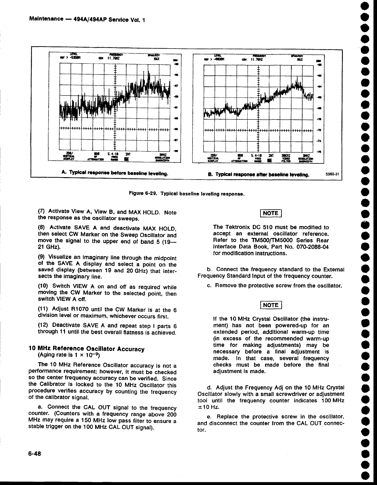
Malntenance
- 494A/494Ap
Servlce
Vol.
1
Figure
6-29. Typlcal basellne teveling response.
o
o
o
a
o
o
o
t
o
t
o
o
o
I
t
o
o
o
o
I
a
o
o
o
o
I
a
o
o
t
t
a
o
o
o
a
o
o
o
o
o
I
o
a
(7) Activate
View
A, View
B, and
MAX
HOLD. Note
the
response
as
th€
oscillator
sw€eps.
(8) Activate SAVE A and deactivate
MAX HOLD,
then select
CW Marker
on
the Sweep
Oscillator and
r_noye
the signal to the upper end of band S (19_
21 GHz).
(9) Msualize
an imaginary
tine
through
the midpoint
of th€ SAVE
A display
and select
a point on the
saved
display (between
t9 and 20
GHz)
that inter_
sects the
imaginary
line.
(10) Switch
VIEW
A on and off as required
white
rnoving
the CW Marker
to the s€lected
point,
then
switch MEW
A ofi.
(11) Adjust
R1070
until the CW Marker
is at the 6
division
level
or maximum,
whichEver
occurs
first.
(12) Deactivate
SAVE A and repeat
step I parts 6
through
11
until
the best
overall
flatness
is achieved.
10 MHr Reference Oscillator Accuracv
(Aging
rate
is 1 x 10-e)
The 10 MHz
Reference
Oscillator
accuracy
is not
a
performance
requirement;
however,
it must be checked
so th€ center
frequency
accuracy
can
be verified. Since
the Calibrator is tocked
to the 10 MHz Osciilator
this
procedure
verifies
accuracy
by counting
the frequency
of the
calibrator
signal.
a. connect
the cAL ouT signal
to the frequency
counter. (counters with a frequency
range above 20i)
MHz
may require
a 150
MHz low pass
filter
to €nsure
a
stable
trigger on
the 100
MHz
CAL
OUT signat).
6-48
The Tektronix DC 510 must be modified
to
accept an external oscillator reference.
Refer to the TM500ffM5000 Series Rear
Interface Data Book, Part No. 070-2088-04
f
or modification
instructions.
b. Connect
the frequency standard
to the Extemal
Frequency
Standard lnput
of
the
frequency
counter.
c. Remove
the
protective
screw
from
the oscillator.
lf the 10 MHz Crystal
Oscillator
(th€
instru-
ment) has not been powered-up for an
extended
period,
additional
warm-up
time
(in excess of the recommended warm-up
time tor making adjustments)
may be
necessary before a final adjustment is
made. ln that case, several frequency
checks must be made before the final
adjustment is made.
d. Adjust
the Frequency
Adj on the 10 MHz
Crystal
Oscillator
slowly
with a small
screwdriver
or adjustment
tool until the frequency
counter indicates 100
MHz
*10
Hz.
e. Replace
the protective
serew in the oscillator,
and
disconnect the count€r
from the CAL OUT
connec-
tor.
+
+
+ll ifl
Itd II
lh t,l['rtflru.d
fl ||' 't
VI[
!|'|n
I
'll I
ll
n
{
{
{t
{
{l
-
..-
4
-a
s.+tc ltrr
A TYptcrl roapoNc betore baceline
lcveting. B. Typlcrl rlrpo€e aftcr barcline lcvcling.
car ll-tqz
rl,,
rl. Arr' IJ,
$flh ft 'I
hhFr
at oE 5.
ruTrcr. t
n
-
-
I
-
-
-tt
-?l
-7a
-I
*tr
rD
t:!,la
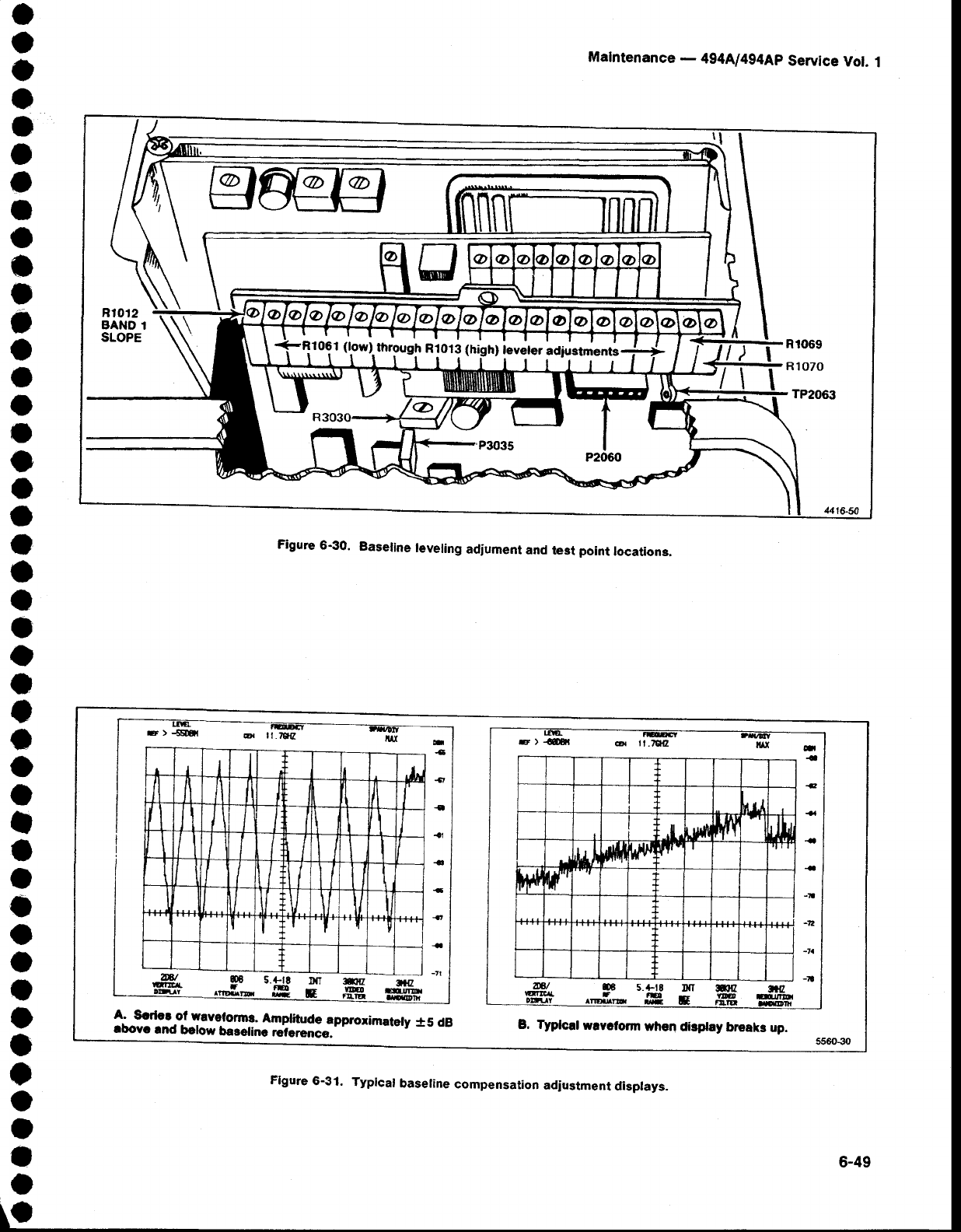
Malntenance
- 494A/4g4Ap
Service
Vot. 1
Figure
6-30. Easeline
leveling
adiument
and
test point locations.
o
o
a
o
t
o
t
o
o
o
I
a
o
a
o
o
o
o
a
o
o
a
a
o
I
I
I
o
o
t
o
a
a
o
o
I
I
I
t
a
I
a
a
I
106l (low) through R1013
(high) leyete, actiustments
It.
,l
tl
ll /1It
tt
tt I
n
'l
-f
I
I1
It
I
tt
U
.u. I
I'f
ltl
-s
{
{
at
<
-
4
{
-71
C
--
<
4
{
{
-il
-t2
.A
-n
F ) .ffl a il.ft1c MI
rrl
ilth
Jdl {tt ll,l
l.r tt'
IrlF' ril",'I 1-
t
Gs.
A- Scrler
ol waveforms.
Amplihrde
approximately
+5 dB
tbovc rnd below
baaeling
reterenc".-- B. Typlcal
wrvclorm when
dirsay bleaks
up.
Flgure 6-31. Typical basetine
compensation adjustrnent
displays.
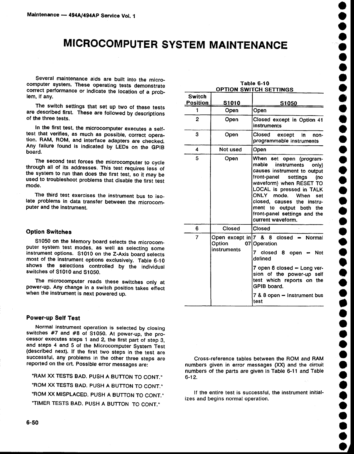
Maintenance
- 494A/4g4Ap
Servtce
Vot.
1a
o
a
a
o
I
I
a
o
e
o
a
o
o
o
o
o
o
a
t
o
o
o
o
o
t
a
o
o
,
t
a
a
o
o
o
o
o
t
o
O
I
o
o
MICROCOMPUTER
SYSTEM
MAINTENANCE
Several maintenance
aids are built
into the micro-
computer syst€m. Th€se operating tssts dEmonstrate
correct performance
or indicate
the location
of a prob_
lem,
if any.
The switch
settings
that set up two of these tests
are
described
first. These
are
followed
by
descriptions
of the
three
tests.
In the first
test,
the microcomputer
executes
a self_
test that verifies,
as much as possible,
correct
opera-
tion. RAM,
ROM,
and interface
adapters
are checked.
Any failure
found is indicated
by LEDs
on the GplB
board.
The second
test
forces
the microcornputer
to cycle
through all of its addresses.
This test requires
less of
the system
to run
than
does
the first
test,
so it may
be
used to troubleshoot
problems
that
disable
the first
test
mode.
The third
test exercises
the instrument
bus to iso_
late problems
in data
transfer
between
the microcom-
puter
and
the instrument.
Option Switches
S1
050 on the Memory
board
selects
the microcom-
puter system
test modes, as well as selecting
som€
instrument
options.
S1
010 on th€ Z-Axis
board selects
rnost ot the instrument
options
exclusively.
Table
6_10
shows the selections controlled by the individual
switches
of
51010 and
S1050.
The microcomputer
r€ads these switches
only at
power-up.
Any change
in a switch position
takes
effect
when
the instrument
is next
powered
up.
Power-up Sell Test
Normal instrument
operation
is selected
by closing
switches
#7 and #8 of Si050. At power-up,
the pro_
cessor
executes
steps
1 and
2, the first
part
of step
3,
and steps 4 and 5 of the Microcomputer
System
Test
(described
next).
lf the first two steps in the test are
successful,
any problems
in the other
three steps are
reported
on
the crt.
Possible
error
messages
are:
"RAM
XX TESTS
BAD.
PUSH
A BUTTON
TO
CONT.'
'ROM
XX TESTS
BAD.
PUSH
A BUTTON
TO
CONT."
"ROM
XX
MISPLACED.
PUSH
A BUTTON
TO
CONT."
TIMER TESTS
BAD.
PUSH
A BUTTON
TO
CONT."
6-50
Cross-reference
tables between the ROM
and
BAM
numbers
given in error messages
(XX)
and the circuit
numbers
of the parts
are
given
in Table
6-11
and
Table
6-12.
lf the
entire
test
is successful.
the
instrument initial-
izes and
begins
normal
operation.
Table 6-1O
SETTINGS
Switch
lesilist
1
s1010
Open
2Open Closed €xcept in Option 41
instruments
3Open Closed except in non-
programmable
instruments
4Not
used Open
5Open When set open (program-
mable instruments only)
causes instrument
to output
tront-panel settings (no
waveform) when
RESET
TO
LOCAL is pressed
in TALK
ONLY mode. When set
closed, causes the instru-
ment to output both the
front-panel
settings
and the
current waveform.
6Closed
'7 Open except
in
Option 07
instruments
7&Sclosed-Normal
Operation
7 closed I open Not
defined
7 open
8 closed
: Long ver-
sion of the power-up
self
test which reports on the
GPIB board.
7 & 8 open
- Instrument
bus
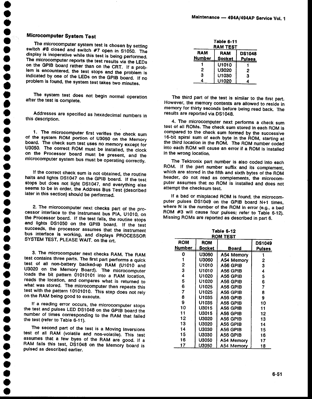
o
I
t
I
I
I
o
I
o
t
o
t
o
o
o
o
o
a
o
a
o
a
o
o
t
a
I
o
t
t
o
I
a
o
o
t
t
3
o
o
o
a
I
t
Microcomputer System Test
.The
microcomputer
system
test
is chosen
by setting
switch
#8 ctosed
and switch
#7 ogen
in S1O6O.
fni
display
is inoperative
while
this
test
is being performed.
The microcomputer
reports
th€
t€st results
via the LEDS
on the GplB board
rather
than on the GRT. lf a prob-
lem is encountered,
the test stops
and
the problem
is
indicat€d
by one of the LEDS
on
itre GptB Ooard. tf no
problem
is
found,
the
system
test
takes
two minutes.
, The system
test
_does
not begin
normal
operation
after
the
test
is complete.
.. . A.ddrelsgs
are
specified
as
hexadecimal
numbers
in
this
description.
l. The microcomputer
first veriftes
the check
sum
of the system
ROM portion
of U30S0
on the Memory
board. The
check
sum
test
uses
no
memory
except
for
U3050.
The correct
ROM
must
be instailed,
the clock
on the Processor
board must be present, and the
microcomputer
system
bus
must
be
operating
correctty.
tf the conect
check
sum
is not
obtained,
the routine
halts
and
lights
DS1047
on the
GplB board. lf the
test
stops but does not tight
DS1O47,
and everything
etse
seems
to be in order,
the
Address
Bus
Test (desiribeo
later
in
this section)
should
be
performed.
2. Tl'rg
microeomputer
next checks part of the pro_
cessor
interface
to the instrument
Uus'pln,
U1010,
on
the Processor
board. lf the
test
fails,
the routine
stops
and lights DS1050
on th€ GptB board. tf the test
succeeds,
the processor
assumes
that the instrument
bus interface
is working,
and displays
PROCESSOR
SYSTEM
TEST,
PLEASE
WA|T.
on the
trt.
3. The
microcomputer
next
checks
RAM.
The RAM
test contains
three parts.
The
first part performs
a quick
test of all non-battery
backed-up
RAM (U10.10
and
U3020 on th€ Memory Board). The microcomputer
loads the bit paftern
01010101
into a RAM tocation,
reads
the location,
and compares
what is returned
to
what
was
stored. The
microcomputer
then
repeats
this
test with
the
pattern
10101010.
This
step
does
not
rely
on
the RAM
being
good
to execute.
. lf a reading
error
occurs,
the microcomputer
stops
the
test and
pulses
LED
DSlO4g
on
the
GplB board
tire
number
of times
corresponding
to the RAM
that failed
the test
(refer
to Table
6-11).
The
second part of the test is a Moving
Inversions
test of all RAM (volatile
and non-volatile).
This test
assumes
that a few byes of the RAM are good. lf a
RAM faits
this test, DS1O4g
on the Memory
board is
pulsed
as
described
earlier.
Maintenance
- 4g4Ll4g4Ap
Service
Vot.
1
The third part of the test is similar
to the first part.
However,
the memory
contents
are
allowed
to reside
in
memory
for thirty seconds
before being
read
back. The
results
are
reported
via
DS104g.
4. The microcomputer
next performs
a check
sum
test of all
ROMs.
The
check
sum
stored
in each
ROM
is
compared
to the check
sum
formed
by the successive
16-bit
spirat
sum of each
byte in tne nOU, starting
at
the third location
in the ROM. The ROM
number
co-ded
into
each
ROM will
cause
an error
if a ROM
is installed
in
the wrong
location.
The Tektronix part number
is also coded into each
ROM. lf the part number
suffix and its complement,
which
are stored in th€
fifth and sixth bytes of the ROM
header,
do not read as complements,
the microcom-
puter
assumes
that no ROM
is installed
and
does
not
attempt
the checksum
test.
lf a bad or misplaced
ROM
is found,
the microcom_
puter pulses DS1049
on the GplB board N+1 times,
where
N is the number
of the
ROM
in error
(e,g.,
a bad
ROM #3 will cause
four pulses;
refer
to Table
Gi2).
Missing
ROMs
are
reported
as
described in
part
6.
Table
6-12
TEST
ROM
0
1
2
3
4
5
6
7
I
9
10
11
12
13
14
15
16
17
ROM
Saakct Board DSl049
u3060
u3060
u1010
u1010
u1020
u1020
ul025
u1025
ul035
ul035
u301
5
u301
5
u3020
u3020
u3030
u3030
u3050
u30s0
A54
Memory
A54 Memory
456
GPIB
456
GPIB
A56 GPIB
A56
GPIB
A56
GPIB
456
GPIB
456
GPIB
A56 GPIB
456 GPIB
456
GPIB
A56
GPIB
A56
GPIB
456
GPIB
456
GPIB
A54 Memory
A54 Memory
1
2
3
4
5
6
7
I
9
10
11
12
13
14
15
16
17
6-51
Tabfe 6-11
u1010
u3020
ul030
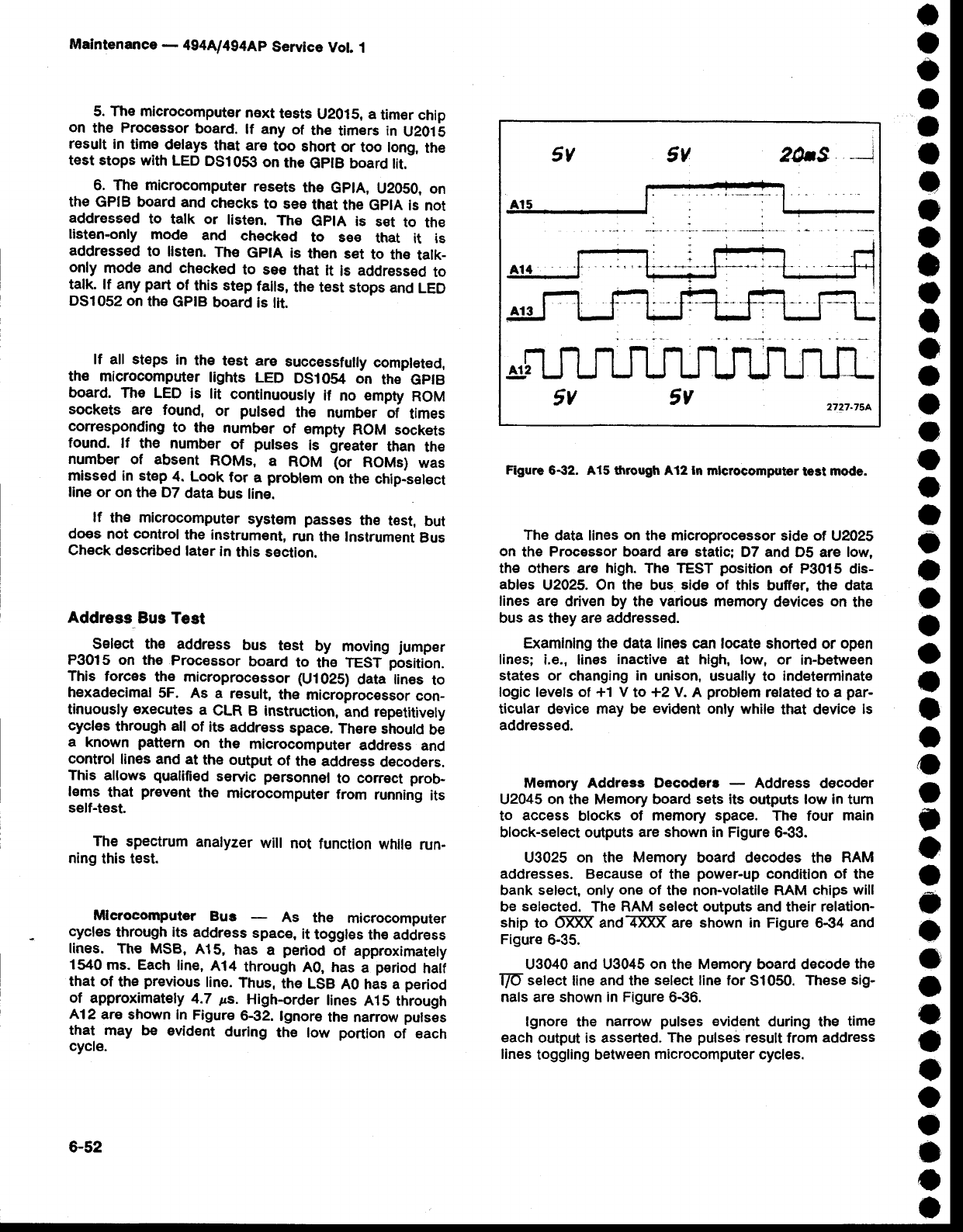
Maintenance
- 494A/494Ap
Service
Vot.
1
!. A" microcomput€r
next
tests
U2015, a timer chip
on th€ Procassor
board.
lf any of the timers
in U201b
result in timo d€lays
that ar€ too short or too long,
the
test stops
with LED
DS10Sg
on th€
GptB
board tit.
6. The microcomputer
resets the GplA, U2050,
on
the
GPIB board and
checks
to see
that
the GptA
is not
addressed
to talk or listen. The GplA is set to the
listen-only mode and checked to see that it is
addressed
to listen.
The GplA is then set to the talk_
only mode and checked to sEe that it is addressed
to
talk. lf any part of this step falls, the test stops
and
LED
DSl052 on
the
GPIB
board is ilt.
lf all steps in the test arE successfully
completEd,
the microcomputer
lights LED DS10S4 on the GptB
board. The LED is lit continuously
if no empty
ROM
sockets are found, or putsed the number of times
corresponding
to the number of empty RoM sockets
found. lf the number of pulses is greater
than the
number of absent ROMs, a ROM (or ROMs)
was
missed
in step 4. Look tor a problem
on the chip-s€lect
line
or on
the D7
data
bus line.
lf th€ microcomput€r
system
passes
the t€st, but
does not control
the instrum€flt,
run the lnstrument
Bus
Check
describ€d
tater
in
this section.
Address
Bus
Test
Select the address bus t€st by moving
jumper
P3015 on the Processor
board to th€ TEST
position.
This forces the microprocessor
(U1025)
data linss to
hexadecimal
5F. As a result, the microproc€ssor
con-
tinuously
executes
a CLR B instruction,
and rep€titively
cycles
through
all of itE
address
space.
There
should
bi
a known pattern on the microcomputer
address and
control lines and at th€ output of th€ address
decoders.
This allows qualified
servic personnel
to corr€ct prob-
l€ms that pr€vont the microcomputer
from running
its
self-t€st.
The spectrum
analyzer
will not function
while
run-
ning
this
test.
Mlerocomputer Bus As the microcomputer
cycles
through
its address
spac€,
it toggles
the address
lines. The MSB, A15, has a period of approximately
1540
ms. Each
line,
414 through
A0, has
a period
haif
that
of the
previous
line.
Thus,
the LSB
A0
has
a period
of approximately
4.7 ps. High-order
lines
A15 through
A12 ara shown in Figure
6€2. lgnore the narrow
pulses
that may be evident during the low portion of each
cycle.
Figure
6-32. A15 through
A12
ln
mlcrocomputor
test
node.
The data lines
on the microprocessor
side of U2025
on the Processor board are static; D7 and D5 are low,
the oth€rs
are high. The TEST
position
of P3015 dis-
ables U2025. On the bus eidE
of this buffer,
the data
lines are driven by the various memory
devices
on the
bus
as
they
are
addressed.
Examlnlng the data lines can locate
shorted or open
lines; i.e., lines inactive
at hlgh, low, or in-between
states or changing
in unison,
usually to indeterminate
logic lev€ts of +1 V to +2 V. A problem
r€lated
to a par-
ticular device may be evident
only while that device
is
addressed.
Memory Address Decoders
- Address decoder
U2045 on the Memory
board sets its outputs low in turn
to access blocks of memory space. The four main
block-select orrtputs
are shown in Figure
6-33.
U3025 on the Memory board decodes
the RAM
addresses. Because of the power-up
conditlon of the
bank
select, only one of the non-volatile RAM
chips will
be selected.
The RAM seleot outputs
and
their relation-
ship to 6-ffi andl{ffi are shown in Figure 6€4 and
Figure
6-35.
U3040
and
U3045
on the Memory
board decode
the
T/O-
select
line and th€
select line for S1050.
These
sig-
nals
are shown
in Figure
6€6.
lgnore the narrow
pulses
evident
during
the time
each
output is asserted.
The
pulses
result from
address
lines
toggling between
microcomputer
cycles.
a
o
o
t
I
o
o
I
o
I
I
I
o
o
o
o
o
o
o
o
a
o
I
o
o
I
a
o
o
I
o
a
c
o
o
o
O
e
o
o
o
o
o
o
6-52
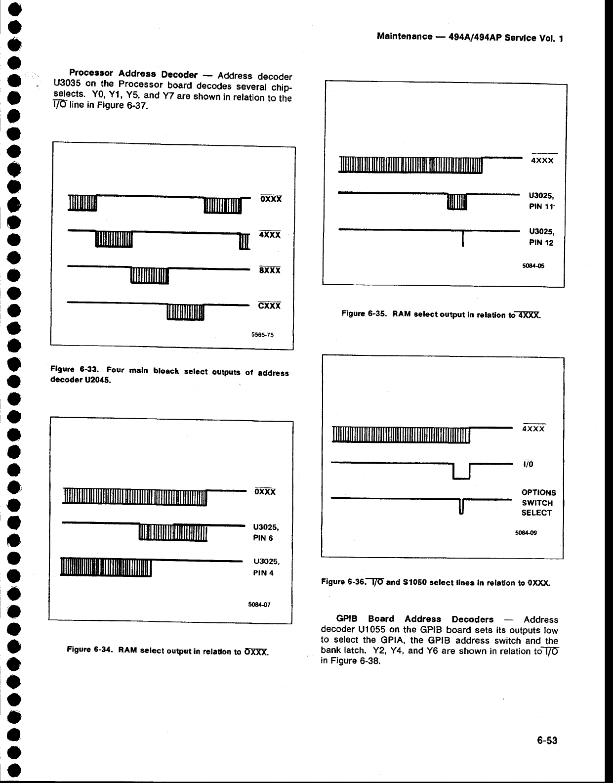
o
o
o
a
t
o
t
I
a
o
o
O
o
I
o
o
o
o
I
I
o
a
o
o
I
a
o
o
o
I
o
O
t
a
a
o
o
o
I
o
o
a
o
a
Processor Address Decoder _ Address decoder
U3035
on the processor
board
decodes
severd chip_
sel€cts.
Y0,
Y'1,
y5, and
y7 are
shown
in
relation
to the
T/6-line
in Figure
6-37.
Flgure 6-33. Four maln bloack select outputs ot address
decoder U20tf5.
Maintenance
- 494A1494Ap
Service
Vot.
.t
Figure
6-35. RAM
select
output in retation
to-llXXX.
Figure
6-36.-Ip and 51050
setect tines
In relation
to 0XXK
GP|B Board Address Decoders Address
decoder
U1055
on the GPIB
board sets its outputs
low
to select
the GPIA,
the GPIB address
switch and the
bank latch. Y2, Y4,
and YG
are shown
in relation
to-TO
in
Figure
6-38.
oxxx
Ixxr
SXXX
erxx
5565-75
----lMm
Itflu|ll
IilMU-
4XXX
lilfi-xilT;
I- u3025,
PIN
12
5S4{5
ililil1Iililt
fl
t
ilfi
il
ilil1ilililil
ilIIilililil1ilil1ilt
Iaxfr.
w
OPTIONS
swtTcH
SELECT
s@4-09
U
0xxx
u302s,
PIN
6
u3025,
PIN
4
5@lL07
Figure 6-34. RAM select ouhut in relailon to dXXX.
6-53
Instrument Bus Test
lf the microcomputer
performs the power-up self-
test, but fails to properly control the instrumeht,
the
instrument bus interface may be faulty. Select the
instrument
bus test by setting the option switch as
shown in Table
6-10.
The microcomputer
continuously
writes
to the instrument
bus in a repetitive
mannert
so
the
instrument
does
not operate normally.
The pattern on the instrument bus toggles DATA
VALID and POLL
and exercises
the address
and data
lines. The address
lines
change
when DATA
VALID
ls
low and the data lines change when DATA VALID
ls
high.
However, if an assembly on the bus is requesting
service because of the way it powered up, DBo-DB4
may continue
to change
after DATA
VALID
goes
low. In
this case, an assembly
or assemblies
may respond
to
the high stat€
of POLL and the changing
state
of AB7
and attempt
to report status.
The pattern
for the upper
address and
data
lines is
shown in Figure
6€9. From
address
or data
line
7 to
linE
0, each line changes
at twic€ the rate of the
previ-
ous lin€, resulting
In 128 cycles on
the LSB
lines. ThE
initial
pulse
on the upper
four data lines is not part of
the +2 pattgrn and is not repeated
on the lower four
data lines. lt is possible
to discover open
or shorted
lines by comparing
the patterns
to those
in Figure
6€9,
checking
that they +t. Look
for lines
that
stay high
or
low, change
together
or at wrong times in the pattern,
or go
to indeterminate
logic levels
(1
V to 2 V).
TROUBLESHOOTING
ON THE
INSTRUMENT
BUS
lnstrument Bus Data Transfers
There are two commands and queries provided
to
aid troubleshooting of circuit functions
controlled by the
instrument
bus. These
circuits
get
data
from
the
micro-
computer or respond
with data
for the microcomputer.
The ADDR
command
and ADDR
query
set and retum
the instrument bus address for the DATA command.
The DATA command
and DATA query set and return
data
on
the
instrument
bus.
Because
th€ DATA command
changes
the
status of internal
hardware,
its use may
prevent normal spectrum Analyzer opera-
tion. Incorrect
,settings
of some hardware
could
cause
instrument damage.
Maintenance
- 494A/494Ap
Servtce
Vol. 1
Chlp relectr Y0, Yl, Y5, and y7 In retadon
to
Flgure
G-38. Chlp
relects Y2,
y4, and
y6 in relation
tilll6.
o
I
o
o
I
o
I
I
O
o
o
I
o
o
o
o
o
o
I
o
e
o
o
o
a
a
a
o
I
I
o
t
I
o
o
o
o
o
o
o
o
a
o
o
Flgurc 6-37.
-rlo.
Clocks and Control
Llnes
- The 680g
clock
input
line should
be a square
wave
with a period
of approxi-
mately
0.293
ps. The
c 2 output on pin
37 shoutd
have
a period
of approximately
1.17;rs.
VMA,
RESET,
NMt,
and
R/W should
be high.
TFd instrument
bus
power
up.
uo
It|l woEm
Yr iffiI
Y5 (70XXl
Y7 offii
556UX)
[[I
t[I[
6-54
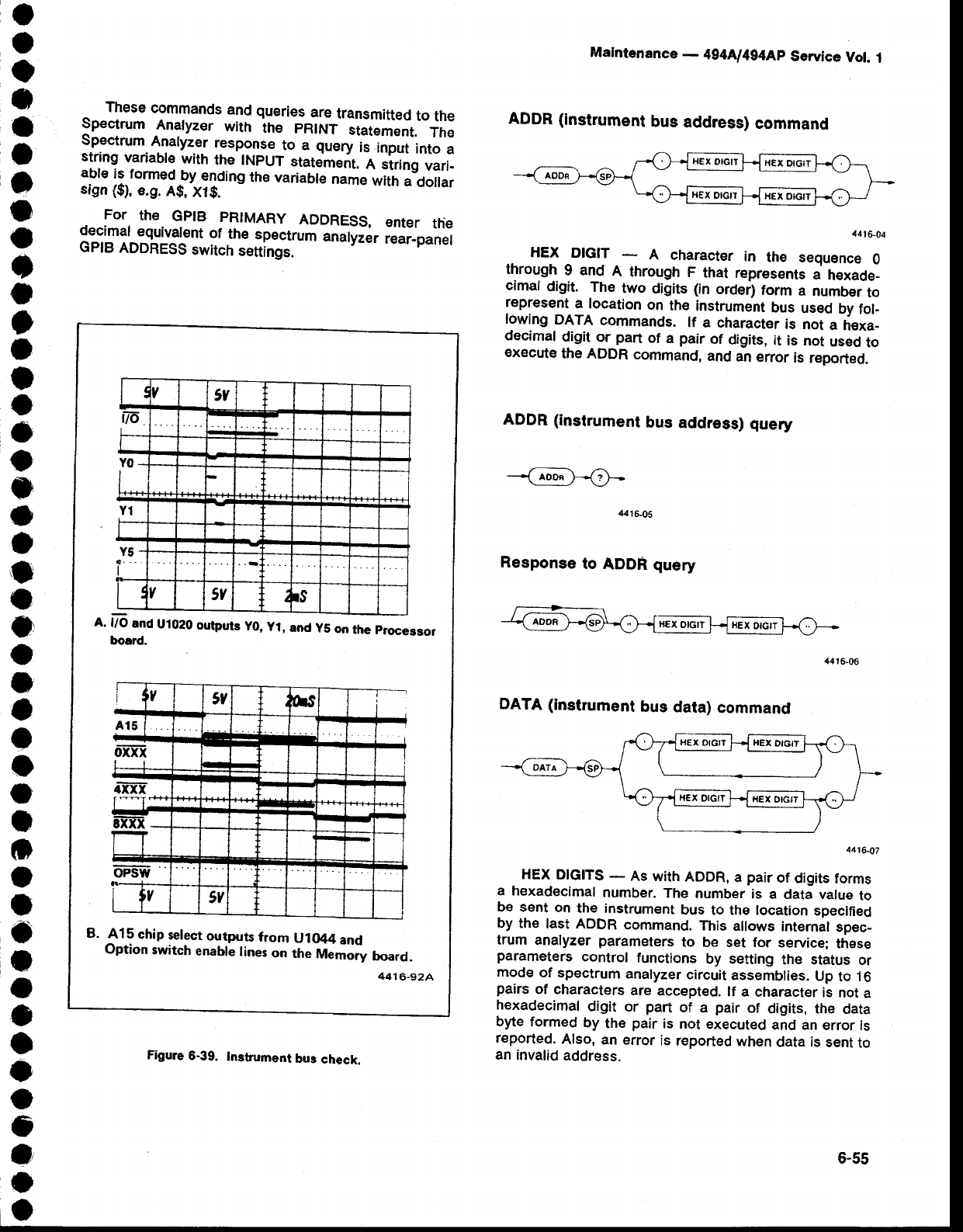
Malntenance
- 4g4N494Ap
Service
Vol.
1
ADDR
(instrument
bus
address)
command
These
commands
and queries
are transmitted
to the
!ryl*rn Anatyzer with ihe pRtNT st#ment. rne
upecrrum
Anatyzer
resp-onse
to a query
is input
into a
string
variable
with
the tNpUT
statement.
A string
vari-
able
is-formeclpV
endinO
th€
variable
name
with
a doilar
sign ($),
€.9.
A$,
Xt$.
FOr thE GPIB PRIMARY ADDRESS,
ENtEr
tIiE
9"_g'g"l equivalent
of the spectrr, "n"lyi"r rear-panel
GPIB
ADDRESS
switch
settings. '.'--'
B. 419 chip
select
outputs
from U1044
and
Uptton
switch
enable
lines
on the
Memory
board.
4416-92A
HEX DIGIT - A character
in the sequence
0
through
9 and A through
F that represents
a hexade_
cimal digit. The two digits (in ordei; torm a number
to
represent
a location
on the
instrument
bus
used
by fot_
lowing DATA commands. lf a character
is not a hexa-
decimal
digit
or part
of a pair
of digits,
it is not
used
to
€xecute
the ADDR
command,
and
an
error
is reported.
ADDR (instrument bus address) query
DATA (instrument
bus data)
command
HEX
DIGITS
- As
with
ADDR,
a pair
of digits
forms
a hexadecimal
number.
The number
is a data
value
to
b€ sent
on the instrument
bus to the location
specified
by the last ADDR
command.
This
allows
internal
spec-
trum analyzer
parameters
to be set for service:
these
parameters
control functions
by setting
the status
or
mode
of spectrum
analyzer
circuit
assemblies.
Up
to .16
pairs
of characters
are
accepted.
lf a character
is not
a
hexadecimal
digit or part of a pair of digits, the data
byte
formed
by the pair
is not
executed
and an
error
is
reported.
Also,
an error
is reported
when
data is sent
to
an
invalid
address.
Response
to ADDR
query
r_----{-a
6-55
Figure
6-39. Insfument bus
check.
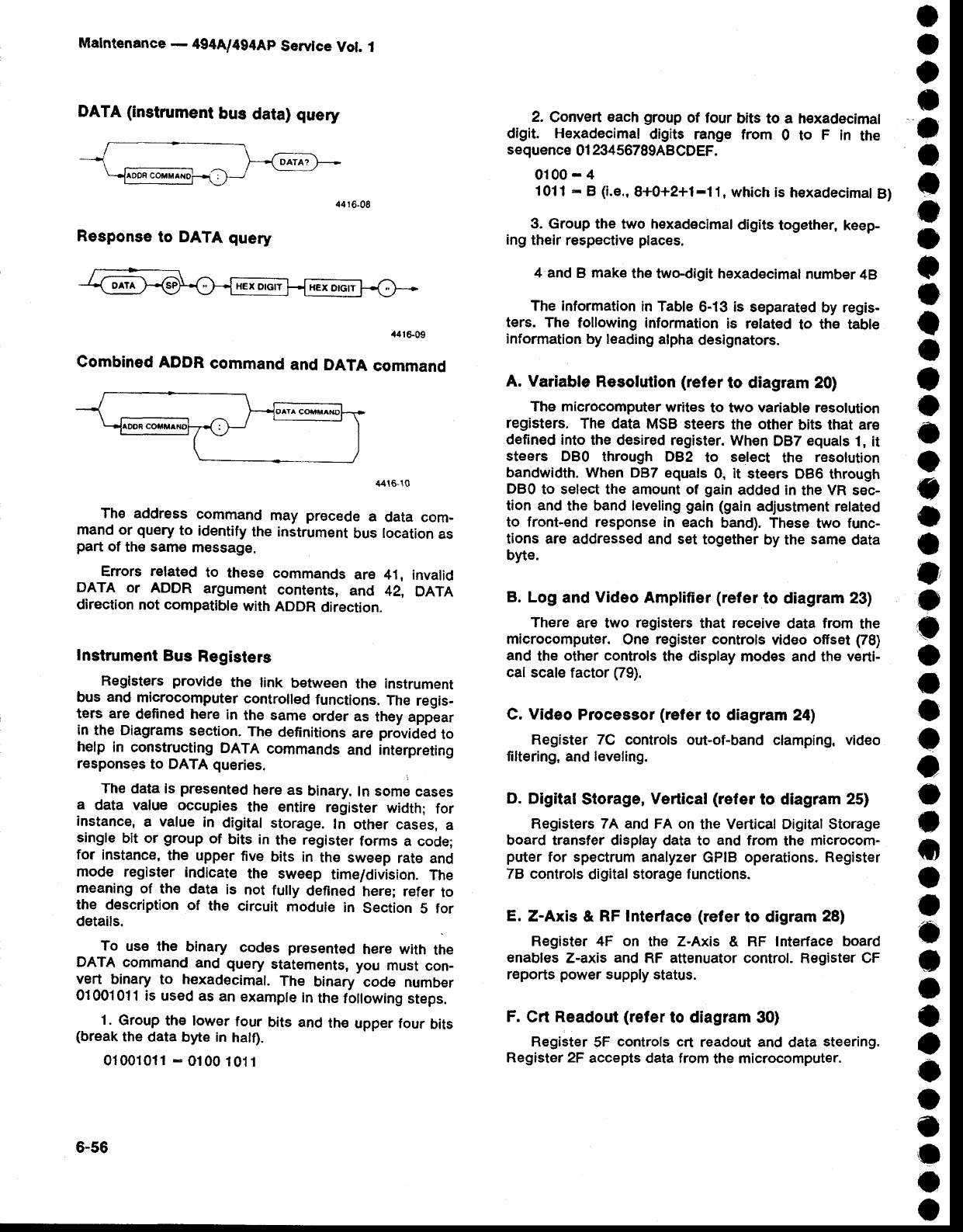
DATA
(instrument
bus
data)
query
l\ F--{ oaraz }-.-
\ -
:^p0RjdglE*tF'
4416-08
Response
to DATA
query
a4t$09
Combined
ADDR
command
and DATA
command
Malntenance
- 494Alttg4Ap
Service
Vol. I
The address
command
may precede
a data com-
mand or query
to identify
the instrument
bus
location
as
part of the same
m€ssage.
Enors related
to these commands
are 41
, invalid
DATA or ADDR argument
contents,
and 42, DATA
direction
not compatible
with
ADDR
direction.
Instrument
Bus
Registers
Registers
provide
the link between
the instrument
bus
and
microcomputer
controlled
functions.
The
regis-
ters are
defined here
in the same
order
as they
appear
in the Diagrams
section.
The
definitions
are provided
to
help in constructing
DATA
commands
and interpreting
responses
to DATA
queries.
The
data is presented
here as binary.
In some
cases
a data value occupies
the entire register
width; for
instance,
a value in digital storage.
tn other cases,
a
single
bit or group
of bits in the register
forms a code;
for instance,
the upper
five bits in the sweep
rate and
mode register indicate the sweep timeldivision.
The
meaning
of the data is not fully defined
here; ref€r
to
the d€scription
of the circuit module
in Section
5 for
details.
To use the binary codes presented
here with the
DATA
command
and query
statements,
you must
con-
vert_
binary to hexadecimal.
The binary
code number
01001011
i$ used
as
an
example
in
the
following
steps.
1. Group
the lower
four bits and
th€ upper four
bits
(break
the data
byte in half).
01001011
- 0100
1011
2. Convert
each
group
of four bits to a hexadecimal
digit. Hexadecimal
digits range from 0 to F in the
sequenc€
01
23456789A8CDEF.
0100
- 4
1011
- B (i.e..
8+0+2+1-11,
which is
hexadecimat
B)
3. Group the two hexadecimal
digits together, keep-
ing
their
respective
places.
4 and
B mak€
the two-digit
hexadecimal
number
48
The infornation
in Table
6-13
is separated
by regis-
ters. The following information
is related to the table
information
by leading
alpha
designators.
A. Variable Resolutlon (refer to diagram 20)
The microcomputer
writes to two variable
resolution
registers. The data MSB steers the other bits that are
defined
into
the desired register.
When
DB7
equals
1, it
steers DBo through DB2 to select the resolution
bandwidth. WhEn DB7
equals
0, it steers DB6
through
DBo
to select
the amount of gain
added in the
VR s€c-
tion and
the band
leveling
gain
(gain
adjustment
related
to front-end
response in each
band).
These two func-
tions are addressed and
set
together
by the
same
data
byte.
B. Log and Video Amplifier (refer to diagram 23)
There are two registers
that receive
data from the
microcomputer. One register controls vid€o offset (78)
and
the other controls
the display modes and the verti-
cal scale factor (79).
C. Video Processor (reler to diagram 24)
Register 7C controls out-of-band
clamping, video
fi
ltering,
and
leveling.
D. Digital Storage, Vertical (refer to diagram 25)
Registers 7A and FA on the V€rtical Digital Storage
board transfer
display data to and
from the microcom-
puter
for spectrum analyzer
GPIB operations.
Register
78 controls
digital
storage
functions.
E. Z-Axis & RF Interface (refer to digram 28)
Register
4F on the Z-Axis & RF Interface board
enables
Z-axis
and
RF attenuator control. Register CF
reports
power
supply status.
F. Crt Readout (refer to diagram 30)
Register
5F controls crt readout and
data
steering.
Register 2F
accepts data
from
the
microcomputer.
o
o
O
o
I
o
o
o
o
o
o
I
o
t
o
a
o
C
o
t
a
o
(l
o
a
o
o
o
o
)
o
o
o
o
t
o
o
o
a
a
C
o
o
o
6-56
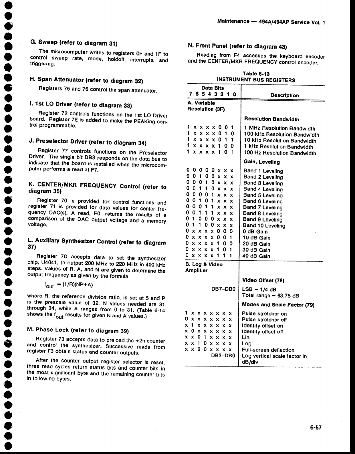
G. Sweep (refer to diagram 3l)
The microcomputer
writes
to registers
0F
and
1F
to
control sweep rate, mode. holdott, interrupts,
and
triggEring.
H. Span Attenuator (refer to diagram 32)
Registers
75
and
76
control
the
span
attenuator.
l. lst LO Driver (refer to diagram 33)
Register
72 controls
functions
on the 1st
LO Driver
board. Register
ZE
is added
to make
the
pEAKing
con-
trol
programmable.
J. Preselector Driver (refer to diagram 34)
Register
77 controls
functions
on the preselector
Driver. The
single
bit DB3
responds
on
the data
bus
to
indicats
that
the board
is instaileO
when
the microcom_
puter
performs
a read
at F7.
K CENTER/MKR
FREQUENCy
Controt (reter ro
diagram 35)
.R€gisjer
70 is provid€d
for control
functions
and
register
71 is provided
for data values
for center
fre_
quency
DAC(s).
A read, F0, returns
the results
of a
comparison
of the DAC
output
voltage
and
a memory
voltage.
L. Auxiliary Synthesizer Control (refer to diagram
371
Register
7D accepts data to set the synthesizer
chip,
U4041,
to output
200
MHz
to 220
MHz
in
400
kHz
steps.
Values
of R,
A, and
N are
given
to determine
the
output
frequency
as
given
by
the
formula
fout : (l/RXNP+A)
where
R, the reference
division
ratio,
is set
at 5 and
p
is the prescale
value of 32. N values
needed
are 3.1
through
34, while
A ranges
from 0 to 31. (fable 6_14
shows
the
fou, results
for given
N
and
A values.)
M. Phase
Lock (refer to diagram
39)
,Register
73
accepts
data
to preload
the
+2n
counter
and control the synthesizer.
Successive
reads from
register
F3 obtain
status
and
counter
outputs.
After the counter
output register
selector
is reset,
three read
cycles
return
status
bits and
counter
bits in
lhg To"l significant
byte
and
the remaining
counter
bits
in
following
bytes.
Maintenance
- 4g4Al4g4Ap
Servlce
Vol.
l
N. Front
Panel
(refer
to diagram
43)
Reading
from
F4 accesses
the keyboard
encoder
and
the
CENTER/MKR
FREQUENCy
controt
encoder.
Tabte
6-13
INSTRUMENT
BUS
REGISTERS
1xxxx001
1xxxx010
1xxxx011
1xxxx100
1xxxx101
Data
Bits
76543210
A. Variable
Resolution
{3F}
B.
Log
& Video
Ampllfier
Description
Resolution Bandwidth
I MHz Resolution
Bandwidth
100 kHz Resotution
Bandwidth
10 kHz Resolution
Bandwidth
1 kHz Resolution
Bandwidth
100 Hz Resolution
Bandwidth
Galn, Levellng
Band 1 Leveling
Band
2 Leveling
Band 3 Leveling
Band 4 Leveling
Band 5 Leveling
Band
6 Leveling
Band 7 Leveling
Band I Leveling
Band 9 Leveling
Band 10
Leveling
0 dB Gain
t0 dB Gain
20 dB Gain
30 dB Gain
40 dB Gain
Video Olfset
{78}
LSB
- 114
dB
Total range
- 63.75
dB
Modes
and
Scale
Factor
O9)
Pulse
stretcher
on
Pulse
stretcher
off
ldentify
offset on
ldentify
offset
off
Lin
Log
Full-screen
deflection
Log
vertical
scale
factor in
dB/div
00000xxx
00100xxx
00010xxx
00110xxx
00001xxx
00101xxx
00011xxx
00111xxx
01000xxx
01100xxx
0xxxx000
0xxxx001
0xxxx100
0xxxx101
0xxxx111
DB7-DBO
lxxxxxxx
0xxxxxxx
xlxxxxxx
x0xxxxxx
xx0lxxxx
xxl0xxxx
xx00xxxx
DB3-DBO
6-57
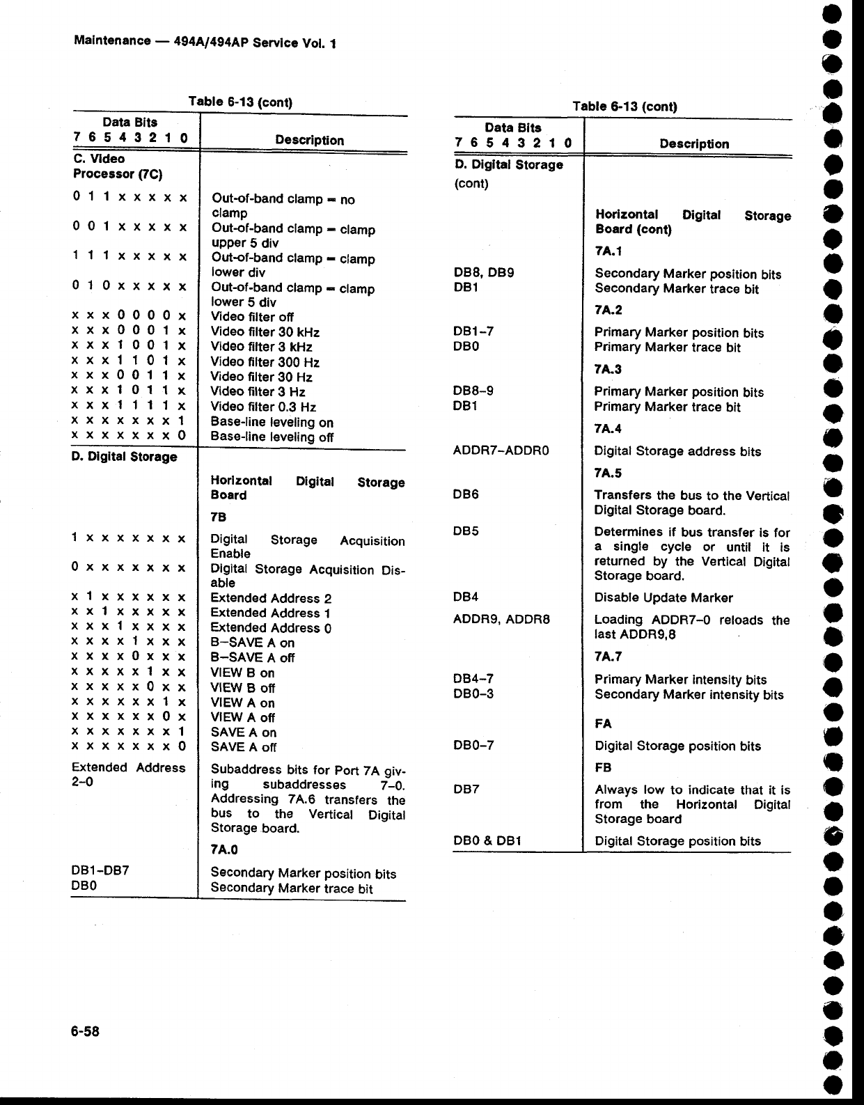
Maintenance
- 494A/494Ap
Service
Vot.
i
Table
6-13
(cont)
Data
Bits
76543210 Description
C. Vldeo
Processor (7C)
011xxxxx
001xxxxx
1l1xxxxx
010xxxxx
D. Dlgital
Storage
o
o
o
a
a
t
t
a
o
I
o
I
o
a
o
o
o
o
I
o
o
o
o
o
o
o
o
a
o
I
o
o
a
e
t
I
o
o
o
o
o
e
o
a
xxx0000x
xxx0001x
xxx1001x
xxx1101x
xxx0011x
xxx1011x
xxx1111x
xxxxxxxl
xxxxxxx0
l xxxxxxx
0xxxxxxx
xlxxxxxx
xxlxxxxx
xxxlxxxx
xxxxlxxx
xxxx0xxx
xxxxxlxx
xxxxx0xx
xxxxxxlx
xxxxxx0x
xxxxxxxl
xxxxxxx0
Extended
Address
2-O
DB1-DB7
DBO
Out-of-band
clamp
- ns
clamp
Out-of-band
clamp
- g;6rt
upper
5 div
Out-of-band
ctamp
- 66rO
lower
div
Out-of-band
clamp
- qlgmt
lower
5 div
Mdeo
filter off
Video
filter
30 kHz
Mdeo
filter
3 kHz
Video
filter
300 Hz
Video
filter
30 Hz
Mdeo
filter
3 Hz
Mdeo
filter
0.3 Hz
Base-line
leveling
on
Base-line
leveling
off
Horlzontal Digital Storage
Board
7B
Digital Storage Acquisition
Enable
Digital Storage Acquisition Dis-
abl€
Extended
Address 2
Extended
Address 1
Extended
Address 0
B-SAVE A on
B-SAVE A otr
VIEW
B on
VIEW
B off
VIEW
A on
VIEW
A off
SAVE
A on
SAVE
A off
Subaddress
bits for Port
7A giv-
ing subaddresses Z-0.
Addressing
7A.6 transfers
the
bus to the Vertical Digital
Storage
board.
7A.0
Secondary
Marker
position
bits
Secondary
Marker
trace
bit
Data
Bits
7654321
D.
Digital
Storage
(cont)
DB8, DBg
DB1
DBl-7
DBO
DB8_9
DB1
ADDRT-ADDRO
DB6
DB5
D84
ADDRg,
ADDRS
DB4-7
DBO-3
DBO-7
DBO
& DBl
Description
Horlzontal Digital Storage
Board
(cont)
7A.1
Secondary
Marker
position
bits
Secondary
Marker
trace
bit
7A.2
Primary
Marker
position
bits
Primary
Marker
trace bit
7A.3
Primary
Marker
position
bits
Primary
Marker
trace
bit
7A,.4
Digital
Storage
address
bits
7A.5
Transfers
the bus
to the Vertical
Digital
Storage board.
Determines
if bus transfer
is for
a single cycle or until it is
returned by the Vertical Digital
Storage board.
Disable
Update Marker
Loading
ADDRT-o reloads
th€
last
ADDR9.8
7A.7
Primary Marker
intensity
bits
Secondary
Marker
int€nsity
bits
FA
Digital Storage
position
bits
FB
Always low to indicate
that it is
from the Horizontal Digital
Storage board
Digital
Storage
position
bits
Table
S13 (cont)
6-58
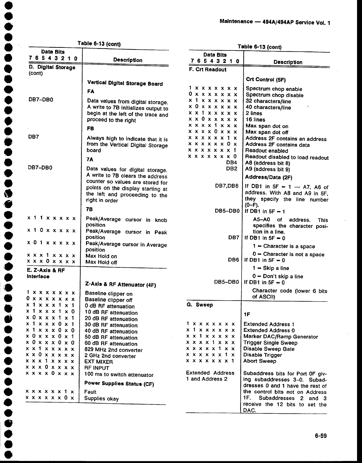
Data
Blts
76549210
D. Digital
Storage
(cont)
DB7-DBO
DB7-DBO
x1'lxxxxx
xl0xxxxx
x0lxxxxx
E. Z-Axls
& RF
Interfaee
Maintenance
- 494A^l494Ap
Service
Vot.
1
Table
&13 (cont)
Table
&13 {cont)
Deseription
Ver$cal
Digltal
Storage
Board
FA
Data
values
from
digital
storage.
A write
to 78 initializes
output
to
begin
at the left of the trace
and
proce€d
to the right
FB
Always
high
to indicate
that
it is
frorn
the Vertical
Digital
Storage
board
7A
Data
values
for digital
storage.
A write
to 78 clears
the
address
counter
so values
are
stored
for
points
on the
display
starting
at
the left and proceeding
to the
right
in
order
7B
Peak/Average
cursor in knob
position
Peak/Average
cursor in peak
position
Peak/Average
cursor
in Average
position
Max
Hold
on
Max
Hold
off
Z-Axis
& RF
Attenuator
{4F)
Baseline
clipper
on
Baseline
clipper
off
0 dB
RF
attenuation
10
dB
RF
attenuation
20
dB
RF attenuation
30
dB
RF
attenuation
40
dB
RF
attenuation
50
dB
RF
attenuation
60
dB
RF attenuation
829
MHz
2nd
converter
2 GHz
2nd
converter
EXT
MIXER
RF
INPUT
100
ms
to switch
attenuator
Power
Supplies
Status (CF)
Fault
Supplies
okay
lxxxxxxx
0xxxxxxx
xlxxxxxx
x0xxxxxx
xxlxxxxx
xx0xxxxx
xxxxlxxx
xxxx0xxx
xxxxxxlx
xxxxxxOx
xxxxxxxl
xxxxxxx0 D84
oB2
Data
Eits
76543210
F.
Crt Readout
DB7.DB6
DB5-DBO
D87
DBO
DB5-DBO
G. Sweep
Extended Address
1 and Address 2
Crt Controt
(5F)
Spectrum
chop
enable
Spectrum
chop
disable
32 characters/line
40
characters/line
2lines
16lines
Max
span
dot
on
Max span
dot ofr
Address
2F contains
an
address
Address
2F
contains
data
Readout
enabted
Reaclout
disabled
to load
readout
A8 (address
bit
8)
A9 (address
bit 9)
Address/Data
(2F)
lfDBlin5F-1-A7,A6of
address.
With
Ag and A9 in 5F,
they specify the line number
(0-F).
lf DBI
in5F-1
A5-40 of address. This
specifies
the character posi-
tion
in a
line.
lf
DBl
in5F-0
1 - Character
is a space
0 - Character
is not
a space
lf DBl
in5F-0
1-Skipaline
0: Don't
skip a tine
lf DBl
in
5F
:0
Character
code (lower
6 bits
of ASCII)
1F
Extended
Address
1
Extended
Address
0
Marker
DAC/Ramp
Generator
Trigger
Single
Sweep
Disable
Sweep
Gate
Disable
Trigger
Abort
Sweep
Subaddress
bits for Port
0F giv-
ing subaddresses
3-0. Subad-
dresses
0 and
t have
the
rest of
the control
bits not on Address
lF. Subaddresses
2 and 3
receive
the 12 bits to set the
DAC.
xxx'txxxx
xxx0xxxx
lxxxxxxx
xlxxxxxx
xxlxxxxx
xxxxlxxx
xxxxxlxx
xxxxxxlx
xxxxxxxl
lxxxxxxx
0xxxxxxx
x1xxx1x1
x1xxx1x0
x0xxx1x1
x1xxx0x1
x1xxx0x0
x0xxx0x1
x0xxx0x0
xxlxxxxx
xx0xxxxx
xxxlxxxx
xxx0xxxx
xxxxOxxx
xxxxxxlx
xxxxxx0x
6-59
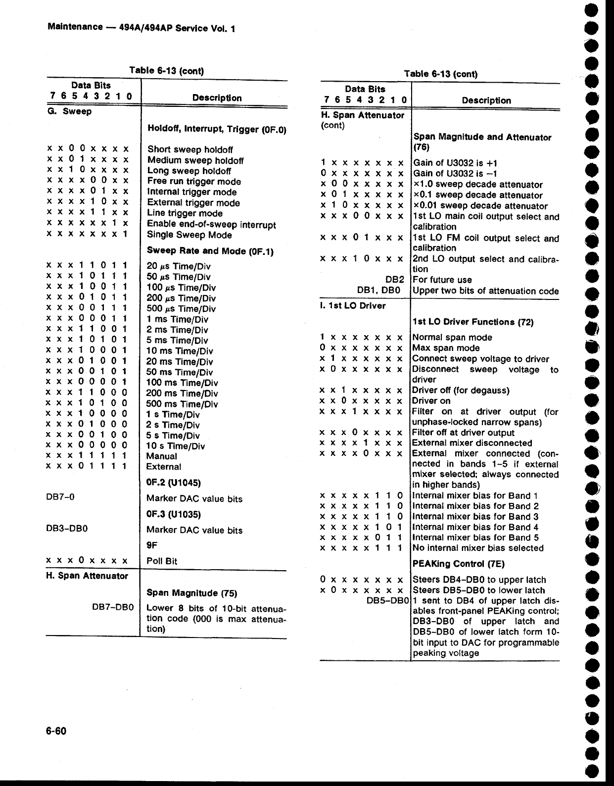
Table
6-13
{cont)
Malntenance
- 494A/4g4Ap
Servlce
Vol. 1
Data
Bits
76549210 Descriptlon
G. Sweep
I
o
o
o
I
o
)
t
o
o
a
o
o
o
o
I
o
I
o
3
a
o
o
o
C
o
o
o
o
a
o
o
o
o
o
o
o
a
a
O
o
o
t
o
xx00xxxx
xx0lxxxx
xxl0xxxx
xxxx00xx
xxxx0lxx
xxxxl0xx
xxxxllxx
xxxxxxlx
xxxxxxxl
0
0
0
0
0
0
1
1
xxx1101
xxx1O11
xxx1001
xxx0101
xxx0011
xxx0001
xxx1100
xxx1010
xxx1000
xxx0100
xxx0O10
xxx0000
xxx1100
xxx1010
xxx1000
xxx0100
xxx0010
xxx0000
xxx1111
xxx0111
Holdoff,
Interrupt,
Trigger (0F.0)
Short sweep
holdoff
Medium
sweep
holdofi
Long
sweep
holdoff
Free
run
trigger
mode
Internal
trigger
mode
Extemaltrigg€r
mode
Line
trigger
mod€
Enable
end-of-sweep
interrupt
Single
Sweep
Mode
Sweep
Rato
and
Mode (0F.1)
20
ps
Time/Div
50
ps
Time/Div
100
ps
Time/Div
200
ps Time/Div
500
ps
Time/Div
1 rns
Time/Div
2 ms Time/Div
5 ms
Time/Div
10
ms
Time/Div
20
ms
Time/Div
50
ms
Time/Div
100
ms
Time/Div
200
ms Time/Div
500
ms
Time/Div
1 s Time/Div
2 s Time/Div
5 s Time/Div
10
s Time/Div
Manual
External
0F.2 (U104s)
Marker
DAC
value
bits
0F.3
(U103s)
Marker
DAC
value
bits
9F
PollBit
DB7-O
DB3-DBO
xxx0xxxx
H.
Span
Attenuator
DB7-DBO
Data
Bits
76543210
H.
Span
Attenuator
(cont)
lxxxxxxx
0xxxxxxx
xO0xxxxx
x0lxxxxx
xl0xxxxx
xxx00xxx
xxx0lxxx
xxxl0xxx
DB2
DBl,
DBO
l. 1st
LO
Driver
0xxxxxxx
x0xxxxxx
DBs-DBO
Descrlption
Span Magnitude
and
Attenuator
(76)
of U3032
is +1
Gain
of U3032 is -1
x1,0
sweep
decade attenuator
x0.1
sweep
decade attenuator
x0.01
swe€p
decade attenuator
l st LO
main
coil output
select
and
calibration
1st LO FM coil output
select
and
calibration
2nd LO output
select
and
calibra-
tion
For
future
use
Upper
two bits
of attenuation
code
lst LO Driver Functions (72)
Normal
span
mode
span
mode
sweep
voltage
to driver
Disconnect sweep voltage to
driver
Driver
off
{for
degauss)
Driver
on
Filter on at driver output (for
unphase'locked
narrow
spans)
Filter off
at driver output
External
mixer
disconnected
External mixer connected (con-
nected in bands 1-5 if external
mixer selected; always
connected
in higher
bands)
Internal
mixer
bias
for Band
1
Internal
mixer
bias
for Band
2
Internal mixer
bias
for Band 3
Internal mixer
bias
for Band
4
lnternal
mixer
bias
for Band 5
No inlernal
mixer bias selected
PEAKing
Control(7E)
Steers DB4-DB0
to upper latch
Steers
DBs-DBo
to lower
latch
1 sent
to DB4 of upper
latch dis-
ables
front-panel PEAKing
control;
DB3-DB0 of upper latch and
DBS-DBO
of lower
latch form 10-
bit input
to DAC
for programmable
peaking
voltage
lxxxxxxx
0xxxxxxx
xlxxxxxx
x0xxxxxx
xxlxxxxx
xx0xxxxx
xxxlxxxx
xxx0xxxx
xxxxlxxx
xxxx0xxx
10
10
10
01
11
11
xxxxx
xxxxx
xxxxx
xxxxx
xxxxx0
xxxxxl
Span Magnitude (75)
Lower 8 bits of 10-bit attenua-
tion code (000 is max attenua-
tion)
Table 6-13
(cont)
6-60
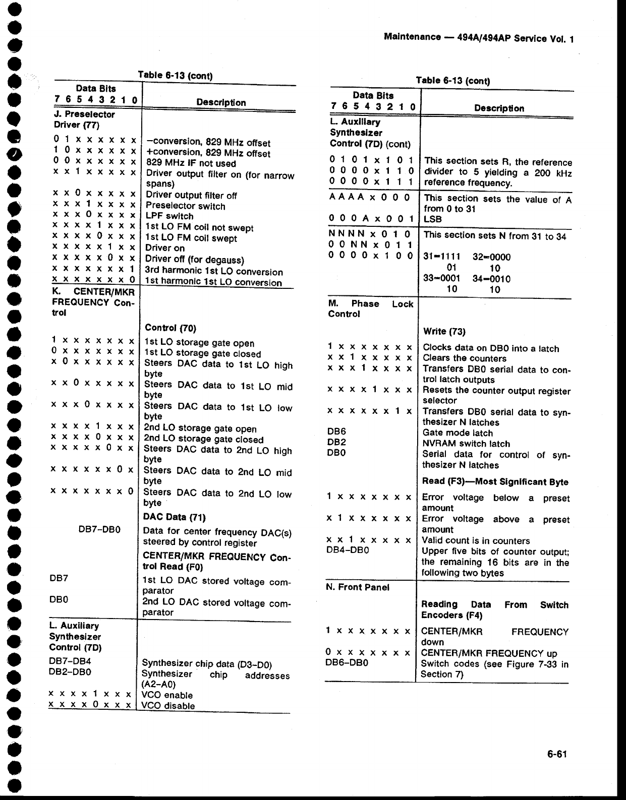
o
o
C
o
I
o
o
C
o
o
o
o
o
a
o
I
O
t
o
J
a
o
o
a
o
o
t
o
t
I
o
o
o
a
o
o
o
o
a
o
o
a
I
o
x
x
x
x
x
x
x
x
x
Data
Bits
7654321A
J. Preselector
Driver
(77)
0lxxxxxx
l0xxxxxx
00xxxxxx
xxlxxxxx
K. CENTER/MKR
FREQUENCY
Con-
trol
lxxxxxxx
0xxxxxxx
x0xxxxxx
xx0xxxxx
xxx0xxxx
xxxxxx0x
xxxxxxx0
DB7-DBO
D87
DBO
L. Auxiliary
Synthesizer
Control
(7D)
DB7-D84
DB2-DBO synthesizer
chip
data
(D3-D0)
Synthesizer chip addresses
x0
xx
xx
XX
xx
xx
xx
xx
xx
X
1
0
x
x
x
x
x
xxx
xxx
xxx
lxx
0xx
xlx
x0x
xxx
xxx
NNNN x 0 t 0
0 0 NN x 01 1
0000x100
X
x
x
x
x
x
x
1
Mafntenanca
- 494A1494Ap
Service
Vol.
1
Table
6-13
(contl
Table
6-13
(cont)
Descrlption
-conversion,
g2g
MHz
ofiset
+conversion,
829 MHz
offset
829
MHz
tF not
usEd
Driver
output filter on (for narrow
spans)
Driver
output
filter
off
Preselector
switch
LPF
switch
lst LO
FM
coil
not
swept
1st
LO
FM
coit
swept
Driver
on
Driver
ofi (for
degauss)
3rd
harmonic
1st
LO conversion
lst LO conversion
Control
(70)
1st
LO
storage
gate
open
1
st LO
storage
gate
closed
Steers
DAC
data to 1st LO high
byte
Steers
DAC data to ist LO mid
byte
Steers
DAC data to 1st LO low
byte
2nd
LO
storag€ gate
open
2nd
LO
storage gate
closed
steers DAC
data
to 2nd Lo high
byte
Steers
DAC
data to 2nd LO mid
byte
Steers
DAC data
to 2nd LO low
byte
DAC
Data (71)
Data
for center
frequency
DAC(s)
steered
by control
register
CENTER/MKR
FREQUENCy
Con-
trol Read (F0)
1st LO DAC
stored
voltage
com_
parator
2nd LO DAC
stored
voltage
com-
parator
Data
Bits
76543210
L Auxlllary
Syntheslzer
Control
(7D)
(cont)
0101x101
0000x110
0000x111
AAAA x 0 0 0
000Ax001
M. Phase Lock
Control
xxxxlxxx
xxxxxxlx
DB6
DB2
DBO
lxxxxxxx
xlxxxxxx
xxlxxxxx
DB4-DBO
N. Front Panel
lxxxxxxx
0xxxxxxx
DB6-DBO
DescripUon
This
section
sets
R,
the reference
divider
to 5 yietding
a 20O
kHz
reference
frequency.
This section
sets the value
of A
from
0 to 31
LSB
This
section
sets
N
from
3.1
to 34
31-1111 32-0000
01 .r0
33*0001 34-0010
10 10
Write
(73)
Glocks
data
on
DBo
into a tatch
Clears
the
counters
Transfers
DBO
serial
data
to con-
trol latch
outputs
Resets
the
counter
output
register
selector
Transfers
DBo
serial
data
to syn-
thesizer
N latches
Gate mode
latch
NVRAM
switch
latch
Serial data for control of syn-
thesizer N latches
Read
(F3)-Most Slgnlficant
Byte
Enor voltage below a preset
amount
Error voltage above a preset
amount
Valid
count
is
in
counters
Upper five bits of counter output;
the remaining
16 bits are in the
following
two
bytes
Reading Data
Encoders
(F4)
CENTER/MKR
down
From Swilch
FREQUENCY
CENTER/MKR
FREQUENCY
up
Switch
codes
(see
Figure 7-33
in
Section 7)
lxxxxxxx
xxlxxxxx
xxxlxxxx
xxxxlxxx
xxxx0xxx
xxxxx0xx
(A2-A0)
VCO
enable
xxxxlxxx
xxxx0xxx vco
6-6r
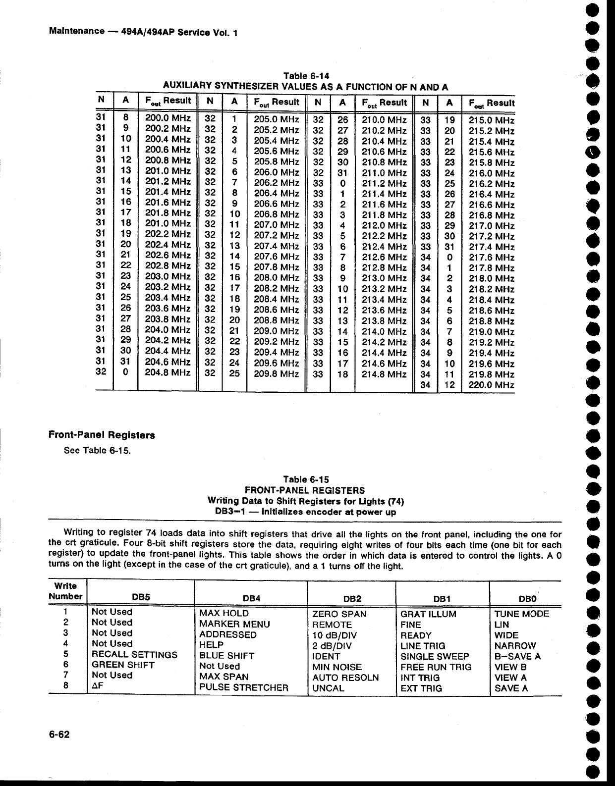
Malntsnance
- 494A/494Ap
Servlce
Vol.
l
Table
6-14
AUXILIARY
SYNTHESTZER
VALUES
AS A FUNCTION
OF N AND A
Front-Panel
Registers
See
Table 6-15.
Table
6-15
FRONT.PANEL
REGISTERS
Writing
Data
to Shift Registers
for Lights
fi4)
DB3-1 - Initiallzes
encoder
at power
up
Writing to register
74 loads
data into
shift
registers
that drive all the lights on
the front
panel,
including
the
one for
the crt graticule.
Four
8-bit
shift
registers
store
the data, requiring eight wlites of four
bits
each
time
(one
bit for
each
register)
to update
the front-panel
lights.
This
table
shows
the order
in which
data is enter€d to control
the lights.
A o
turns
on the light
(except
in
the
case
of the
crt graticule),
and
a 1 turns
off
the
light.
o
I
o
o
o
I
)
o
o
o
o
e
t
a
o
o
o
o
o
I
a
o
o
o
I
o
t
o
a
t
I
o
a
a
t
o
o
a
a
o
o
o
t
o
NAF*, Result NAFou, Result NAFou, Result NAFooi Result
31
31
31
31
31
31
31
g1
31
31
31
31
31
31
31
31
31
31
31
31
31
31
31
31
32
I
I
10
11
12
13
14
15
16
17
18
19
20
21
22
23
24
25
28
27
28
29
30
31
0
200.0
MHz
200.2
MHz
200.4
MHz
200.6
MHz
200.8
MHz
201.0
MHz
201.2
MHz
201.4 MHz
201.6
MHz
201.8
MHz
201.0
MHz
202.2MH2
202.4 MHz
202.6
MHz
202.8
MHz
203.0
MHz
2O3.2MHz
203.4
MHz
203.6
MHz
203.8
MHz
204.0
MHz
2O4.2MHz
204.4 MHz
204.6
MHz
204.8
MHz
92
32
32
32
32
32
32
32
32
32
32
92
32
32
32
32
32
92
32
32
32
32
32
32
32
1
2
3
4
5
6
7
I
9
10
11
12
13
14
15
16
17
18
19
20
21
22
29
24
25
205.0 MHz
205.2MH2
205.4
MHz
205.6
MHz
205.8
MHz
206.0
MHz
2O6.2MHz
206.4
MHz
206.6
MHz
206.8
MHz
207.0 MHz
207.2MH2
2O7.4MHz
207.6
MHz
207.8
MHz
208.0 MHz
208.2MH2
208.4 MHz
208.6
MHz
208.8
MHz
209.0 MHz
2O9.2MHz
209.4 MHz
209.6
MHz
209.8
MHz
32
92
32
32
32
32
33
33
33
33
33
33
33
33
33
33
33
33
33
33
33
33
33
33
33
26
27
28
29
30
31
0
1
2
3
4
c
6
7
I
9
10
11
12
13
14
15
16
17
18
210.0
MHz
210.2MH2
210.4
MHz
210.6
MHz
210.8 MHz
211.0 MHz
211.2MH2
211.4
MHz
211.6 MHz
211.8
MHz
212.0
MHz
212.2MH2
212.4 MHz
212.6 MHz
212.8MH2
213.0 MHz
213.2MH2
213.4 MHz
213.6
MHz
213.8
MHz
214.0
MHz
214.2MH2
214.4
MHz
214.6 MHz
214.8
MHz
33
33
33
33
33
33
33
33
33
33
33
33
33
34
34
g4
34
34
34
34
34
34
34
34
34
34
19
20
21
22
a
24
25
26
27
28
29
30
3l
0
1
2
3
4
5
6
7
I
9
10
11
12
215.0
MHz
215,2MH2
215.4 MHz
215.6
MHz
215.8
MHz
216.0
MHz
216.2MH2
216.4
MHz
216.6 MHz
216.8
MHz
217.0 MHz
217.2MH2
217.4 MHz
217.6
MHz
217.8MH2
218.0 MHz
218.2MH2
218.4
MHz
218.6
MHz
218.8 MHz
219.0
MHz
219.2MH2
219.4 MHz
219.6 MHz
219.8 MHz
220.0
MHz
Wrlte
Number DB5 DB4 DB2 DB1 DBO
1
2
3
4
5
6
7
I
Not Used
Not Used
Not Used
Not Used
RECALL SETTINGS
GREEN
SHIFT
Not Used
AF
MAX HOLD
MARKER
MENU
ADDRESSED
HELP
BLUE
SHIFT
Not Used
MAX SPAN
PULSE STRETCHER
ZERO
SPAN
REMOTE
10
dB/Drv
2
dB/DrV
IDENT
MIN
NOISE
AUTO
RESOLN
UNCAL
GRAT ILLUM
FINE
READY
LINE TRIG
SINGLE SWEEP
FREE
RUN
TRIG
INT TRIG
EXT TRIG
TUNE MODE
UN
WIDE
NARROW
B_SAVE A
VIEW B
VIEW A
SAVE A
6-62
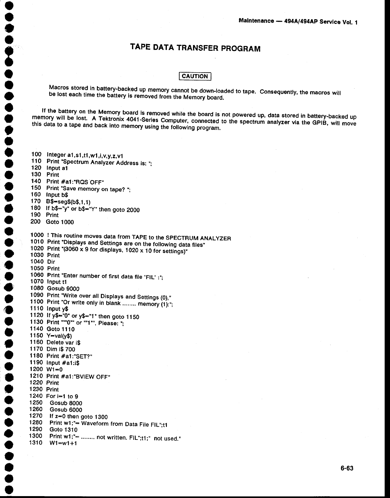
I
o
J
o
I
I
t
I
o
O
o
)
I
I
J
t
o
o
o
o
I
o
o
o
I
o
t
o
o
I
o
o
I
a
J
)
o
o
o
o
o
a
a
I
Maintenance
- 4g4ful4g4Ap
Service
Vol. 1
TAPE
DATA
TRANSFER
PROGRAM
Macros
stored
in battery-backed
up memory
cannot
be
down-loaded
to tape. consequenfly,
the macros
will
be lost each
time
the battery
is removed
from
ttre f_Aemory
UoarO.
lf the battery
on the Memory
board is removed
while
the board
is not.powered
up,
data
stor€d
in battery-backed
up
memory
will be lost' A Tektronix
4041'series
computer,
"onn""t"a to the spectrum
analyzer
via
the GplB, will move
this
data
to a
tape
and
back
into
memory
using
the
tottowing piogr"rn.
109 lntegeral
,sl
,tl,wl
,i,v,y,z,vl
119 Print
"Spectrum
Analyzer
Address
is:
,,;
PA lnput
al
130 Print
140 Print
#al:.ROS
OFF"
150 Print
"Save
memory
on
tape? ";
160 Input
b$
174 B$-seg$(b$,.t,1)
19q !j b$-"y"
or b$-',y,,
then
goto
2000
190 Print
20O Goto
1000
1000 ! This
routine
moves
data
from
TApE
to the
spEcrRUM ANALYZER
I919 !1"t "Disptays
and
Settings
are
on
the
foilowing
data fites"
1020 Print
*(3060
x 9 for displays,
1020
x t0 tor settiigsl; --
1030
Print
1040
Dir
1050
Print
1060
Print
"Enter
number
of
first
data
file,FlL,
:,,;
1070
Inputtl
1080 Gosub
9000
1090 Print
"Write
over
all
Displays
and
Settings
(0),,,
1100
Print'Or
write
only
in
b1ank........
memory
(1):,,;
1110
tnput y$
11?9 lf y$:"0' or
y$-,'1"
then
goto
1 1S0
1130 pfint
uuuO*"
Of
,,,,1 ,,,,,
pleasl: ,,:
1140
Goto
1110
1150
Y:vat(y$)
1 160 Detete
var
ig
1170
Dim
i$
700
1180
Print
#al:"SET?,,
1190
lnput
#al:i$
1200
w1-0
1210
Print
#ai:"BVtEW
OFF,'
1220 pilnt
1230
Print
124O
For
i:l to 9
1250 Gosub
8000
1260 Gosub
6000
1270 lf z-0 then
goto
I3O0
1280 Print
w1;': Waveform
from
Data
File
FtL';tl
1290 Goto
1310
1300 Print
w1
:n: ........
not
written.
FlL,,;tl;,,
not
used.,,
1310 Wl-w1+1
6-53
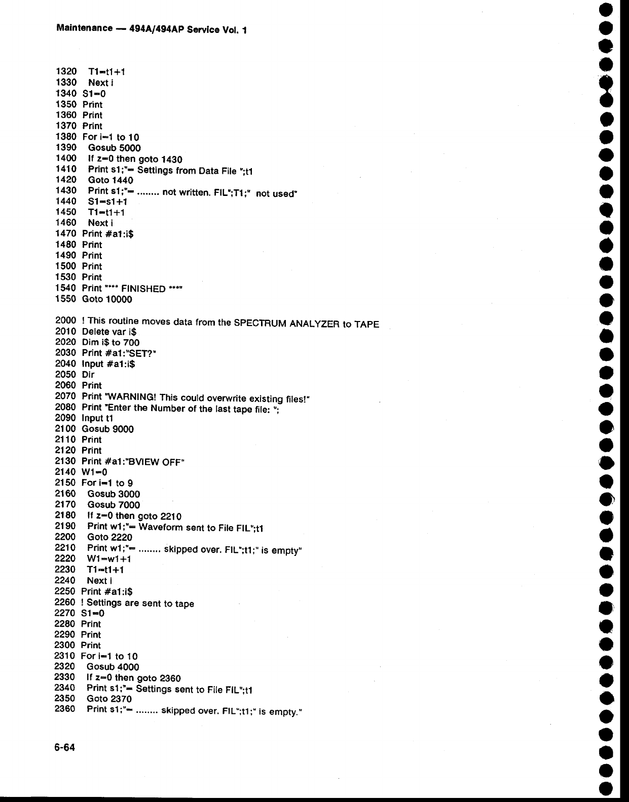
Maintenance
- 4g4[l4g4Ap Servlce
Vot.
1
1320 T1-t1+1
1330 Next
i
13a0
S1:0
1350
Print
1360
Print
1370
Print
1380
For i-1 to 10
1390 Gosub
5000
1400 lf z-0 then
goto
1400
1410 Print
s1;'- Settings
from
Data
File
";t1
1424 Goto 1440
14i10 Print
s1
;"-........
not
written.
FIL';TI;,.
not
used"
1440 S1-sl+1
1450 T1-t1+1
1460 Next
i
1470
Print
#al:i$
1480 Print
1490
Print
1500
Print
1530 Print
1540
Print
o*r
FINISHED
*rn
1550 Goto 10000
2000 !This routine
moves
data from
the
spEcrRUM ANALYZER
to TAPE
2010
Delete
var
i$
2020 Dim
i$
to 700
2030 Print
#at:"SET?"
2040
Input
#al:i$
2050 Dir
2060 Print
2070 Print'WARNING!
This could
overwrite
existing
files!"
2080 Print
'Enter
the Number
of the last
tape file:
',f
2090 Input
t1
2100 Gosub
9000
2110
Print
2120
Print
2130
Print #a1:"BVtEW
OFF,'
2140
W1:0
2150
For
i-l to g
2160 Gosub
3000
2170 Gosub
7000
2180 lf
z-0 then
goto
2210
21
90 Print
wl;': Waveform
sent
to File
FlL,,;tl
22A0 Goto2220
2210 Print
wl;":.,...... skipped
over.
FlL";t1;',
is
empty*
2224 Wl:w1f1
2230 T1-tl+1
2240 Next
i
2250 Print
#a1:i$
2260 | Settings
are
sent
to tape
2270 S1-o
2280 Print
2290 Print
2300 Print
2310
For i-1 to 10
2320 Gosub
4000
2330 lf z:0 then
goto
2360
2340 Print
sl;"- Settings
sent
to File FlL,,;tl
2350 Goto 2370
2360 Print
sl
;"- ........
skipped
over.
FlL";t1
;,'
is
empty.,'
6-64
o
o
e
o
o
a
o
o
o
o
o
a
t
a
o
I
o
o
a
O
a
o
a
o
o
o
I
o
t
a
t
o
o
t
e
o
o
a
o
o
o
a
o
o
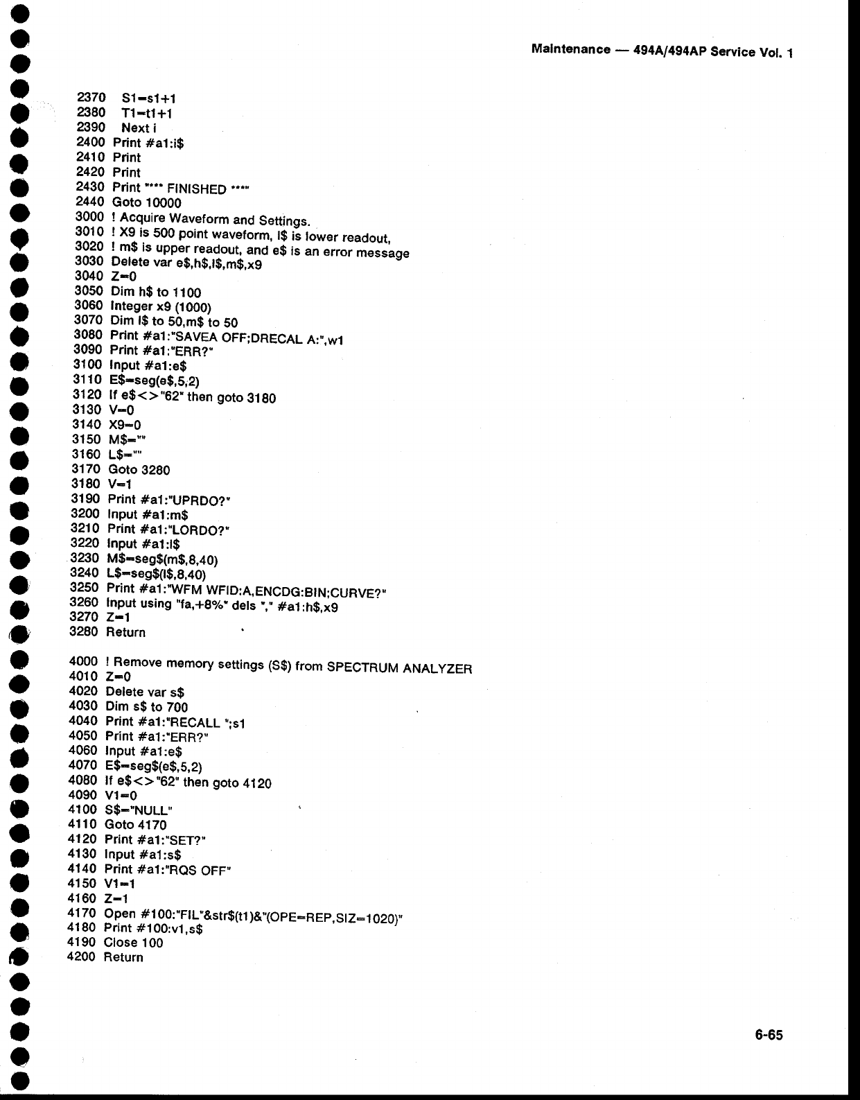
o
o
t
o
I
I
o
o
o
t
a
t
a
I
)
I
a
t
o
a
t
a
o
o
t
o
o
o
o
t
)
o
I
o
)
o
o
o
o
o
o
a
o
t
237A
2380
2390
2400
2410
2420
2$A
2440
3000
3010
3020
3030
3040
3050
3060
3070
3080
3090
3100
31
10
3120
3130
3140
3150
3160
3170
3180
31
90
3200
3210
3220
3230
3240
3250
3260
3270
3280
51-sl+1
T1-tl+1
Next
i
Print
#a1:i$
Print
Print
Print "...
FINISHED'.."
Goto 10000
! Acquire
Waveform
and
Settings.
i X?
i.r
500
point
waveform,
t$
G tower
readout,
lm$ is
upper
readout,
and
€g
is
an
er-i i"""ag"
Delete
var
eg,hg,lg,m$,x9
Z-O
Dim
h$
to
1100
Integer
x9 (1000)
Dim
l$
to So,m$
to 50
Print
#a1
:"SAVEA
OFF;DRECAL
A:",wl
Print
#al:"ERR?"
Input
#al:eg
E$*seg(e$,5;2)
lf
e$<>'62'then
goto
3190
v-0
X9:0
M$-""
L$*",'
Goto
3280
V-1
Print
#al:"UPRDO?"
lnput
#al:m$
Print
#al:"LORDO?'
Input
#a1:l$
M$-seg$(m$,8,40)
L$-seg$(l$,8,40)
PTint
#a1
:NVFM
WFID:A,ENCDG:BIN;CURVE?..
lnput
using "la,*Bo/o'dels
'," #al :h$,x9
Z-1
Return
Mafntenance
- 494A1494Ap
Service
Vot.
1
4000 ! Remove
memory
settings
(S$)
from
SPECTRUM
ANALYZER
4010
Z-0
4020 Delete
var
sg
4030 Dim
s$
to 700
4040
Print
#al :'RECALL,,:s1
4050
Print
#a1:.ERR?,
4060
Input
#al:eg
4070 E$-seg$(e$,S,2)
4080
lf e$<>'62" then
goto
4120
a090
V1:0
4100
S$-"NULL"
4110
Goto
4170
4120
Print
#al :,,SET?,'
4130
Input
#a1:s$
4140
Print
#al:"ReS
OFF"
4150
V1-1
4160
Z-1
41
70 Open #1
00:"FtL"&str$(r1)&'{opE:REp,stz_1
020),,
4180
Print
#100:v'l,s$
4190
Close 100
4200 Return
6-65
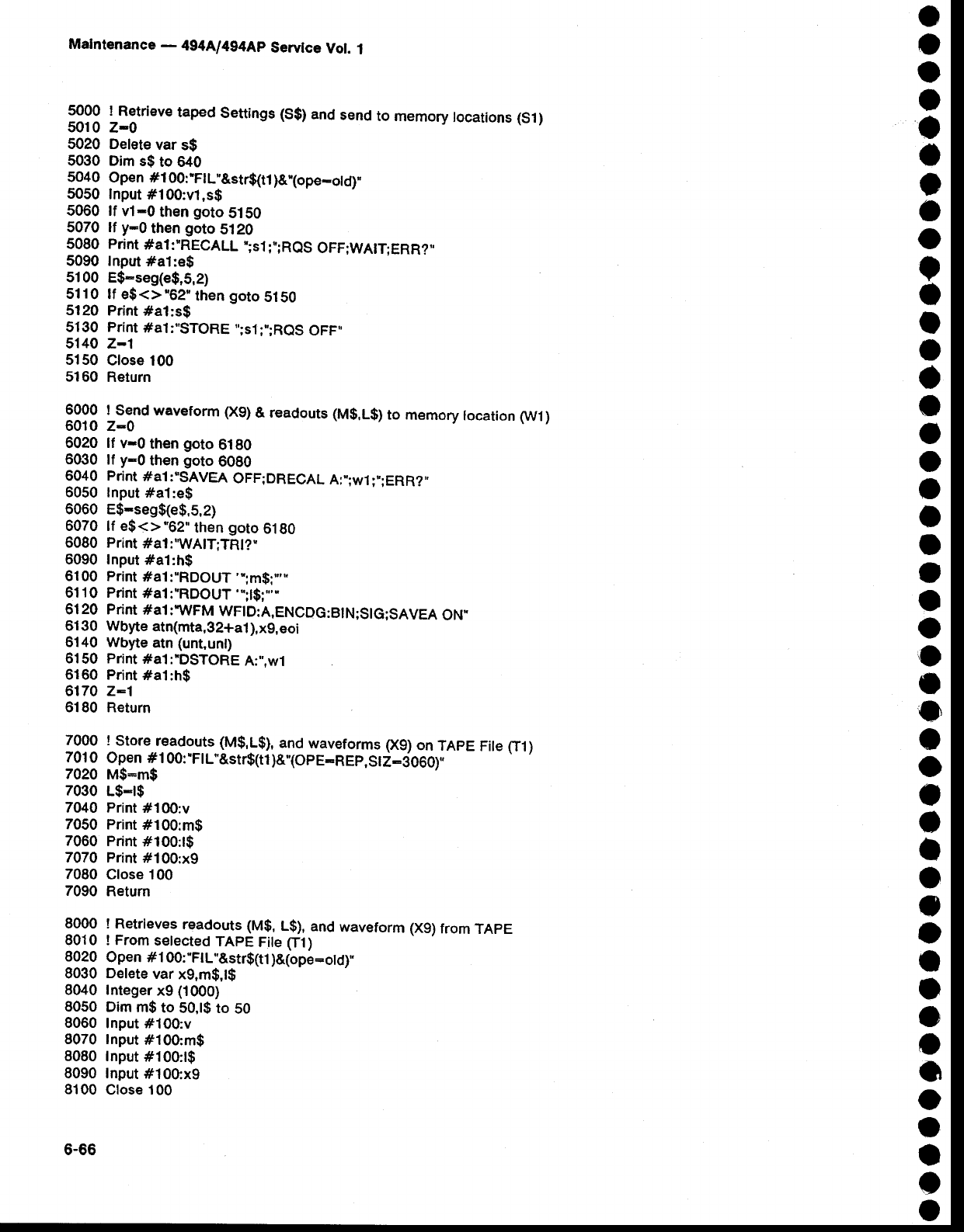
Malntenance
- 494[l4g4Ap Servtce
Vot.
1
5000 ! Retrieve
taped
settings (s$)
and
send
to memory
tocations (s1)
5010
Z-0
5020 Delete
var s$
5030 Dim
s$ to 6zt0
5040 Open #100:"FtL"&st6(t1)&'(ope-otd),,
5050
Input
#100:v1,s$
5060 lf v1-0 then
goto
SiSO
5070 lf Y-0 then
goto
5120
5080
Print
#a1:"RECALL
";s1
;,';ReS
OFF;WAIT;ERR?,
5090 Input
#al:e$
5100 E$:seg(e$,S,2)
5110
lf e$<>"62'then
goto
51S0
5120
Print
#a1:s$
5130
Print
#a1:"STORE
";s1;":ReS
OFF,,
5140 Z-1
5150
Close 100
5160
Return
6000 I Send waveform
(X9)
& readouts
(M$,L$)
to memory
tocation
(Wl)
6010
z:0
6020 lf v-0 then
goto
6180
6030 lf Y-0 then
goto 6080
6040
PriNt
#A1
:'SAVEA
OFF;DRECNL
A:";Wl;',;ERR?,,
6050 Input
#a1:e$
6060 E$-seg$(e$,5,2)
6070 lf e$<>"62"
then
goto
6190
6080 Print
#al:"WA|T:TR|?"
6090 Input
#a1:h$
6100 Print
#al :"RDOUT'";69.t';r,
61
10 Print
#a1:'RDOUT',,;l$;"'"
61
20 PriNt
#A1
:NVFM
WFID:A,ENCDG:BIN;SIG;SAVEA
ON-
6130 Wbyte
atn(mta,32+a1),x9,eoi
6140 Wbyte
atn
(unt,unt)
6150 Print
#a1:'DSTORE
A:...wl
6160 Print
#a1:h$
6i7a z-1
6180 Return
7000 ! Store
readouts (M$,L$),
and
waveforms
(X9)
on
TApE
Fite
(I1)
701
0 Open #1
00:'FtL"&strg(tl)&,IopE-REp,St2_doOO).
7020 M$:m$
7030 L$-t$
7040 Print
#100:v
7050 Print
#100:m$
7060 Print
#100:l$
7070 Print
#100:xg
7080
Close 100
7090 Return
8000 ! Retri€ves
readouts
(M$,
L$),
and
waveform
(X9)
from
TApE
8010 ! From
setected
TAPE
Fite
[r1)
8020 Open #1
00:"FtL"&strg(tl
)&(ope-otd)',
8030 Delete
var
x9,mg,tg
8040 lnteger
x9 (1000)
8050 Dim
m$
to SO,tg
to SO
8060
Input #100:v
8070 Input
#100:m$
8080
Input
#100:t$
8090 Input
#100:x9
8100
Close 100
6-66
o
o
o
I
a
o
)
o
o
?
t
I
t
o
o
o
o
o
a
O
a
O
o
o
I
o
a
o
o
o
I
o
f
I
I
o
o
o
o
o
o
a
t
o
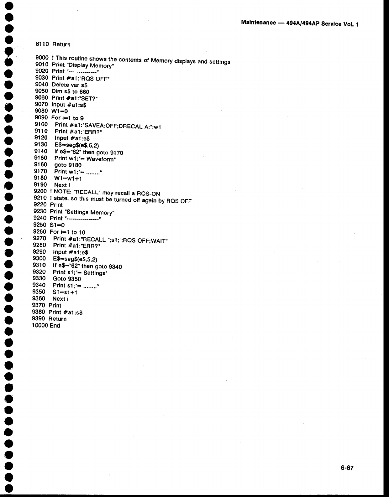
o
o
o
o
t
I
o
I
o
o
o
t
o
o
t
I
o
o
o
o
o
a
a
o
t
o
o
o
o
a
a
o
o
o
a
o
a
o
o
o
o
a
o
o
8110
Return
9000 ! This
routine
shows
the
contents
of Memory
disprays
and
settings
9010
Print
"Disptay
Memory',
9020 Print
9030
Print
#al:,'ReS
OFF'
9040 Delete
var
sg
9050 Dim
s$ to 660
9060 Print
#a1:"SET?'
9070
Input
#at:s$
9080
Wl-0
9090 For
i:t to 9
9100 Print
#at:,SAVEA:OFF;DRECAL
A:";w1
9110 Print
#al:"ERR?"
9120 Input
#a1:eg
9130 E$-s€gg(e$,5,2)
9140 if e$:"52' then
goto
9170
9150 Print
w1;"- Waveform"
9160 goto
9180
9170 Printwl;"*.........
9180 Wl:w1+1
9190 Next
i
9200 ! NOTE:
"RECALL"
may
recail
a RQS_ON
9210 ! state,
so
this
must
be
turned
otf
atain by
ReS
OFF
9220 Print
9230 Print "settings
Memory.'
9240 Print
9250
51-0
9260
For
i-l to 10
9270 Print
#a1:"RECALL',;st;',;ReS
OFF;WA|T,,
9280 Print
#al:,,ERR?"
9290 Input
#al:e$
9300 E$-seg$(e$,5,2)
9310 lf e$-'62" then
goto
9g4O
9320 Print
sl:"- Settings,,
9330 coto 9350
9340 Print
sl;"- ........'
9350 S1-sl+1
9360 Next
i
9370 Print
9380 Print
#a1:sg
9390 Return
10000
End
Maantenance
- I94Al4S4Ap
Service
Vol. 1
6-67

o
a
o
o
?
o
o
a
o
o
o
o
O
o
t
o
o
o
o
o
a
o
o
o
o
a
o
o
o
o
o
o
o
o
I
o
o
a
t
o
o
a
o
o

O
o
o
o
o
a
o
o
o
O
o
a
o
o
o
t
a
o
o
a
o
o
o
o
o
o
o
a
o
O
a
o
o
o
o
a
a
o
o
O
a
o
o
o
First, Second, and Third Converters
Swept-frequency
anatysis
is achieved
by a triple-
conversion
superheterodyne
technique. Each of 'the
three
frequency
converters
consists
of a rnixer,
a local
oscillator,
and
appropriate
filters. Only one
frequency
is
converted
in each mixer to pass through
bind_piss
filters
to the detector. This frequency
can
be changeO
by tuning
the local oscillator
trequency
in the first or
second
convErters.
The third converter
uses
the fixed
100
MHz calibrator
signal
as a stable
local oscillator.
An external
source
may
also
be used
as
a reference
for
the 100
MHz calibrator
and
third converter.
The first converter.
usually referred
to as the front
end,.
converts
the input signal frequency
to an inter-
mediate
frequency
(tF)
of either
g2g
MHz or ZO72
MHz,
depending
on which
band is in use. The internal
mixer
converts
signals
over the input range
of 10kHz to
21
GHz. External
mixers
may be used
for signals
into
the millimeter
wavelengths.
When
the internal
mixer
is
used,
a preselector
or low-pass
filter
is inserted
in the
signal path
to reduce
unwanted
signals
or images
and
spurious
responses.
One of two second converters is automatically
selected
for each band so the input fr6quency
range
does not overlap
the first lF frequency.
Each second
converter
has its own local oscillator (LO),
mixer,
and
filters.
Both
down-convert
the signal
to 110 MHz
which
is sent
to the
third
converter.
The
third
converter
amptifies
the
110
MHz
lF signal
and converts
it to the final intermediate
frequency
of
10
MHz. The third converter
passes
the signal
to the
Secton 7 - 494A1494Ap
Service,
Vot.
1
THEORY
OF
OPERATION
This
section
describes
the
spectrurn
analyzer
circuitry.
The
section
begins
with
a functional
description
of
the
maior
circuit
blocks' This
is
fotloweJ
6y'ror" detailed
descriptions
of the circuitry
within
each
block.
while
reading
these
descriptions,
refer
to the coresponding
block
or schematic
diagram
in volume
2 of the
service
Manual'
The
description'tittes
use
ir,e
oi"grar nam-es
and
numbers
for
easy
reference.
The Functional
Block
diagram,
located
at the front
of the Diagrams
section
in Volume
2. shows
how
the
major
sections
in the instrument
relate
andihe.paths_of
*o.1 r-"pr signals.
Block
diagrams
showing
more
L::*;ffi?#:llr:*tions rollow
ttre
Functiinat
Brock
oiagr;;. Gircuit
schematicliasrams
ror6w
the
Adjacent
to each
schematic
is a third
level
of block
diagram,
a circuit
board
parts
location
illustration,
and
cross-reference
look-up
tables.
The
third
level
block
diairam'snows
the function
of the Lornpon"nt"
shown
on
the
schematic'
The
parts
location
illustration
ano
tooi-uf t"or". aid
in finding
components
on either
the
schematic
or circuit
board.
FUNCTIONAL
DESCRI
PTION
What lt Does
The spectrum
analyzer
accepts
an electrical
signal
as its input
and displays
the signal,s
frequency
com_
nn:t:.9n a crt. Signats
can
beapptied
direcily
to the
RF
fNPUT
or
through
an
external
mixer.
The
display
of the input
signat
appears
on
the
crt as
a graph
where
the horizontal
axis
is'frequ€ncy
and
the
v.ertjcal
axis
is arnptitude.
The
disptay
can
be
ptotted,
i,
desired,
by connecting
a chart recorder
througn
rear_
panel
connectors.
The
display
can
also
be transmitted
digitally
via a |EEE
4gg
Geneiar
purpose
Interface
Bus
(GPIB)
to a GptB-compatible
ptotter.
The programmable
version
can be operated
either
T:H"lll.*jih front-panet
controts,
or remotety
via rhe
\rFtE
wtrn
an
easy_to_use
programming
language.
How lt Works
The Spectrum Analyzer operates as a swept,
narrow-band
receiver.
The
crt beam
moves
norizontatty
as a range
of frequencies
is spanned.
When a fre_
quency
component
of an input
signat
is detected,
the
beam
is
deflected
vertically
as
a fuiction
oi inprt power
at
that frequency.
Frequency
is measured
by
counting
the local
oscilla-
tor lrequencies
against
a reference.
Amplitude
is
meas-
ured by catibrating
the REFERENCE
LEVEL
and RF
attenuator.
A master
microcomputer
performs
control,
storage,
signal processing,
and communications
func_
tions.
7-1

Theory
of Operation
- 494A/494Ap
Service,
Vol. 1
main
lF section
for processing
and
detection.
lF Section
This section processes
the signal for frequency
resolution. Several functions are performed here:
bandwidth filtering, amplitude calibration
and loga-
rithmic conversion,
and
signal
detection.
The 10
MHz lF signal
is processed
through
one of
sev€ral
band-pass
filters
selected
by the RESoLUTIoN
BANDWIDTH
control. In the auto mode
the microcom_
puter
will sel€ct
the
best combination
of bandwidth
and
sw€ep
time for the
selected
span,
unless
overridden
by
the operator.
Weak
signals
can be amplified
by a set of switch-
able amplifiers
so the dynamic
display
range
(v€rtical
window) ls shifted up or down. The REFERENCE
LEVEL control selects
th€
gain
and
input
RF attenuation
to frame
this window
between
the reference
lev€l
at th€
top
of the display
screen
and
the bottom
of the display.
A leveling circuit
helps
provide
flat frequency
response
across
the range. The signal is amplified
by a loga-
rithmic amplifier
to produce
the
vertical
signal
calibrat€d
in dB/div.
The detector produces
a voltage that corresponds
to th€ input
signal
strength
in decibels.
The detector
output
is then sent
to the
vertical
channel
of the
display
section
to drive the vertical
axis of the crt and
display
the
signal.
Display Section
The display section
draws the signal on the crt
screen. Vertical deflection
of the beam (y axis) is
increased as th€ output of the amplitude
detector
increases.
The horizontal position
(X
axis)
of a signal
is
controlled by th€ frequency controt section and
corresponds
to the frequency
of the detected
signal.
The Z axis, or brightness,
is controlled
by th€ INTEN_
SITY
control
and
the Z axis
blanking
circuits.
(However,
marker
brightness
is actually
controlled
by stopping
the
digital storage
sweep
for a period of time to brighten
the spot.)
As the spectrum
analyzer
spans
from low to high
frequencies
the beam sweeps
from left
to right. When
the spectrum
analyzer
tunes
through
a signal
frequency,
a vertical
deflection
shows
the strength
of the signal.
The result is a signal
displayed
at a position
on the
span that corresponds
to its frequency,
or in other
words,
the display
shows
amplitude
as
a
function
of fre-
guency.
O
o
o
o
O
o
o
o
o
o
o
O
o
o
o
a
o
o
a
o
o
o
o
o
o
o
o
o
a
o
o
O
a
o
o
O
o
o
o
o
o
o
o
o
7-2
The video
amplifier
scales
the detector output
for
vertical
deflection
in dB/div or performs
a log/linear
conversion,
depending
on the vertical
display
mode.
The video processor provides additional bandwidth
filtering it either
the wide
or narrow
filter is selected.
The display
section also provides
crt readout
to
show control settings and measurement
data. This
readout
is based
on
data
from
the microcomputer
which
is reading
the settings of the front panel
controls
or
data
on
the instrum€nt
and
GPIB buses.
Digital
storage
circuits
provide
two functions;
they
provide a flicker-free
display at slow sweep rates,
and
they store the display
for later viewing. Up to nine
different displays
with their readouts can be stored in
the battery-powered
memory. The stored display
data
can then be transmitted through the IEEE-488
port to a
plotter,
or for programmable
instruments
to GPIB com-
patible
controllers or instruments.
Frequency
Control Section
The
spectrum
analyzer
sweeps through a frequency
range
that
is set by the frequency
control
section.
The
CENTER/MARKER FREQUENCY
control sets the fre-
quency
the
l st and
2nd local
oscillators.
The output of a sweep generator is scaled by a
span attenuator
to sw€ep
a range
or span
of frequen-
cies. The output of the span attenuator
drives the lst
LO for wide spans and the 2nd LO for narrow spans.
The output
sweep
also deflects the crt beam
across
the
horizontal axis as the local oscillators
ar€ swept so the
display
is a spectrum of power
versus frequency.
The frequency control section also tunes the
pr€selector
so it tracks the signal frequency
being
detected over
the
1.7
to 21 GHz range.
Counter and Phase Lock Section
The Counter,
Harmonic Mixer, and Auxiliary
Syn-
thesizer form the nucleus of the frequency control
hardware.
Both the
l st LO and 2nd
LO frequ€ncies are
controlled via the firmware-based control loop. Oata
from the Counter
is used as feedback
to control
the
oscillator
frequency. Accurate
signal frequency
meas-
urement
is possible
by counting
the frequency of the
3rd
lF.
The Phase Lock system stabilizes
the 1st Lo fre-
quency. This minimizes
display
jitter and increases
resolution.
o
o
o
o
o
o
o
o
o
o
o
o
o
o
o
o
o
o
o
o
o
o
o
o
o
o
o
o
o
o
o
o
o
o
o
o
o
o
o
o
o
o
o
o
Digital Control Section
Operational modes and internal functions of the
spectrum
analyzer
are selected
and controlled
directly
from
the front panel. The
modes
anO
tunctions
that
are
selected
are processed
and
activated
by the
instrument
master
microcomputer
which
tarks
and
iisten"
to ail cir_
cuits
over
the instrument
bus. ttre progiammable
ver_
sion can also be remotely
controlled
frim an external
controiler
through
the IEEE_4gg
(GplB)
connector.
This
connector
interfaces
to the instrument
microcomputer
through
the
GptB.
Front
panel
control
and sel€ctor
data
is processed
by a front panel
CpU that interrac""
*itt the master
microcomputer
over the instrument
bus. The master
microcomputer
receives
and
sends
all of its information
over the instrument
bus to th€ intemal
circuits. The
programmable
version communicates
with
other
instru-
m€nts
through
the
GplB connector.
The programmable
control
language
corresponds
to tront_panel
controfs.
Theory
of Operation
- 4g4A/4g4Ap
Servlce,
Vol.
.l
Power Supply Section
The power supply s€ction
provides
regulated
dc
power
and forced
air cooting
for all circuits
within
the
instrument.
The switching
suppty
is capabte
of provid-
ing regulated
voltages
over
a wide range of input
line
frequencies
and
voltages.
The
cooling
system
consists
of an intake
on the bottom
of the cise, air passages
within
the instrument,
a fan,
and a rear
panel
exhaust.
Air is routed
to all sEctions
of the instrument
in propor-
tion
to th€ heat
generated
by circuits
within
thoie sec-
tions. Internal
temperature
variations
are minimized
to
provide
reliable
operation.
Other Sections
Interconnections
between assemblies
are made
through
a common
Mother
board. Most circuit
board
assemblies
plug
into
the top side
of the Mother
board.
Assemblies
on the RF deck
are
connected
to the bot-
tom side
of the Mother
board
through
cables
and
con_
nectors.
7-3
Theory
of Operation
- 4g4Ll4g4Ap
Service,
Vot.
1
DETAILED
DESCRIPTION
The following
description
is arranged
by sections
or systems;
such
as lst Converter, 2nd
Converter,
etc.,
followed
by circuit
analysis
of the circuiis
within
that
section. Each system
or section
is introduced
with
a
description
of the system
using
the section
block
diagram
found
in
ihe oiagrams
section of the Service
Manual,
Volume
2. This
is followed
by
a description
of Lach
cireuit
board or miajor
circuit
within
the system.
The appropriate
block or schematic
diagram
number
is included
in the text h6adings
for each section
or
part.
1ST
CONVERTER
SECTTON
(Diagram
2)
The 1st Converter
consists
of the 0-60
dB step
Atenuator, PreseleCtor,
lst Mixer, .lSt LO, power
Divider,
Transfer
Switch,
2.OT2
GHz Directional
Filter.
Diplexer,
and two 4.5
GHz
Low-pass
Filters. Externai
circuits
that control
or drive
the assemblies
within
the
l st Conv€rter are: the preselector Driver, 1st LO
Driver,
Counter
and phase Loek system,
and the RF
Interface
board.
The 1st
Converter
converts
the
incoming
RF
signals
to the lst lF. lncoming
signals
are applied
through
a
calibrated
0-60 dB decade
attenuator
(AT10)
to a fitter
select switch (S12). Signats
in band t (t
O
k|-tz
to
1.8GHz)
route
through
a Limiter
(A10)
and 1.gGHz
Low-Pass
Filter (FLl0) to the .tst
Mixer (A12).
Signats
in bands
2 through
S (1.7
to 21
GHz)
route
through
a
tunable Preselector
(FL12) and a g dB Attenuator
(4T11)
to
the mixer.
The RF signals
mix with the output
from a tunable
localoscillator
(A16)
to generate
products
at one
of two
intermediate
frequencies,
depending
on the band
in
use.
The 1st Mixer output goes to Directional
Filter
FL16
through Transfer Switch S1B. The transfer switch
allows
input
from the EXTERNAL
MTXER
input,
except
in Option
07 and 08 instruments.
In Option
0Z anO
0g
instruments, the EXTERNAL MTXER capability is
deleted.
The EXTERNAL
MIXER
input
permits
an external
lF
source
(external
mixer)
to be connected
to the instru_
ment. The lF signals
from external
mixers
are routed
through
the Transfer
switch to the Directional
Filter.
This feature
allows much higher input frequencies
by
using
waveguide
mixers.
The direetional
filter separates
the 2OTZMHz
and
829
MHz intermediate
frequencies
for the 2072 MHz
2nd Converter
(A18)
or 829 MHz 2nd Gonverter
(A23).
The 2072 MHz lF is apptied
through
a 4.5
GHz Low_
Pass
Filter
(FLl1)
to the
2072
MHz 2nd
Converter.
The
829
MHz lF is fed through a Diptexer (A14)
and
another
4.5GHz
Low-Pass
Fitter (FL1S)
before
it is apptied
to
the 829 MHz
lF stages.
7-4
The spectrum
analyzer
uses two intermediate
fre-
guencies
(2472
MHz and 829 MHz)
to prevent
basetine
rise caused
by local
oscillator f€edthrough
and cross-
over of intermodulation
products. The 2072
MHz lF is
selected
for band I and for bands
5 and above. The
829 MHz lF is select€d
for bands
2-4.
RF Interface
Circuits
(Diagram
28)
The
RF interface
circuits receive
instruction
from
the
microcomputer
and produce
control
signals for the RF
Attenuator,
the Transfer Switch, and the lF Select.
These
RF control circuits
are located on
the Z-Axis/RF
Int€rface
board
(A70)
and their operation
is described
under
the
z-Axis
board
part
of th€
Display
section.
lst Converter
(Diagram
12)
RF Input
The
RF INPUT
50()
connector accepts
the
input
sig-
nals in bands 1 through 5. Higher frequencies
require
external waveguide mixers that use the EXTERNAL
MIXER input,
along with the
LO
outputs.
Option 07 instruments
have
a75A input
in place
of
the EXTERNAL
MIXER connector. Transfer
Switch S13
selects between
the 50O
and
75O inputs.
The RF input signal
goes through
a 0-60 dB Step
Attenuator
(AT10)
consisting of relay-controlled
10d8,
20 dB, and
30
dB sections. The relays are
actuated
by
control signals
from
the
RF Interface circuit.
Preselector
Circuits
Coaxial switches
31
1 and
512
are relays
that
select
either
the low-pass filter
(FLl0) and Limiter (A10)
or the
Preselector
and
3 dB attenuator
(AT11)
for the RF sig-
nal path. The relay coils are driven by circuitry on the
Preselector Driver
board. The low-pass
filter path is
used for band 1, and the Preselector
path
is used
for
bands 2
through
5.
a
o
o
o
o
o
o
o
o
o
o
o
o
o
o
o
o
o
o
o
o
o
o
o
o
o
o
o
o
o
o
o
o
o
O
o
o
o
o
o
o
o
o
o
o
o
o
o
o
o
o
o
o
o
o
o
o
o
o
O
o
o
o
o
o
o
o
a
o
o
o
o
o
o
a
o
O
o
o
o
o
o
o
o
o
o
o
o
_ The 2GHz Limit€r
(A10)
operates
from 100
kHz to
2 GHz. lt has
a linear
two-port
transfer
characteristic
of
unity (-1 dB) until
the input exceeds
+5 dBm. Above
this point, the internai detEctor OioOes
conduct,
reflecting
part of the RF input energy back to the
source..
A: lhe input
level rises,
the-Limiter
reflects
more
signal,.limiting
the amount
that can pass
through
the mixer,
thus protecting
the mixer
from being
over_
driven.
The 1.gGHz Low-pass
Fitter (FL10)
strips the
incoming
signal
of any frequen"y
cbmpon"nts
above
1.9 911.
and
passes
dtt
treiueniy
"olnion"nt.
o"ro*
1.8
GHz
to Fitter
Setector
swiicn
Si2.
The presetector
(FL12)
is a 1.7-1g
GHz yttrium_
lron-Garnet
(ylG)
filter
that
provides
nigh
setectivity
anO
y1S"-jl"qyency rejection. Tuning
c-urrent,
which is
near
500 mA at 21
GHz,
is provideJ
by the
preselector
Driver (A42) circuits. The presele"ior op"rates on
bands
2, g, 4, and
S. Because
the
preselector
is sensi-
tive
to output
toad
impedance,
a g dB Attenuator
(AT11)
is inserted
between
the
pr€s€lector
output
and
one
port
of the Fitter
Select
switch
to hetp
isotate
output
loading.
1st Mixer
The 1st Mixer
{A12)
circuit
consists
of a single
bal_
anced
mixer,
a coupler,
and
a g0o
phase
shifter.
A bal-
anced
mixer inherently
has less
conversion
loss
com_
Par€d to an unbalanced
mixer, and local oscillator
feedthrough
to ths RF port is minimized.
The locat
oscillator
input is split through a broad-band
multi-
section
coupler
whose
outpute
are equal
in power
but
9p deoqegs.
out of phase. an aOOiitonat
tiO
degree
phase
shift is cascaded
with the appropriate
signal
to
create a 180 degree
phase
difference
ttrat
is ipptied
across
a pair
of series-connected
Schottky
diodes.
The
result
is that
the
diodes
are
alternatety
switcned
on
and
off
as
the local
oscillator
cycles.
The node
between
the two diodes
is isotated
from
11"-,,1^"j !O ^ilpu. by about O0
dB so the RF input is
apptteo
to this node. The blocking
capacitor
at the
input connector
permits
broadband
signal
application
from
the
RF
port,
while
blocking
the
dc'diode
bias
from
g.etting.
to the RF port
and
the
ipectrum
analyzer
input.
Mixer
bias is supplied
from
the
ist LO Driver
board
via
the
829
MHz
lF circuits,
4.5
GHz
Filter,
Diplexet,
Direc_
tional
Filter,
and
Transfer
Switch.
Bias
return
is
through
assembly
A1
1
to
ground.
Excluding
losses
in the lF filtering
circuitry,
the fun_
dam€ntal
conversion
loss
of ths l st
-Conuener
is about
14
dB, and
the
third
harmonic
conversion
loss
is
about
24.d8. The.
Schottky
diodes
are mounted
in a mixer
suo-assembty
(A12A1)
so that they can be easily
replaced.
Theory
of Operation
- 4g4Al4g4Ap
Servtce,
Vot l
1st Local Oscillator
The lst LO (A16)
is a ytG (yttrium-tron-Gamet)
oscillator
that has a tuning range
of 2.072
to 6.4
GHz.
The oscillator
assembly
includes
the interface
circuit
board
that couples
operating
and
tuning
voltages
from
the l.st LO Driver, Span
Attenuator,
and Error
Amptifier
circuits
to the oscillator.
The
+15
Vl voltage
provides
operating
bias
for the
p,l"jl1!or.- The_
suppty is protected and iecoupted by
VRl
010,
Cl
0t
6, and
L1
01
1.
Th: s9c9nd
suppty,
+t S
t2:
is not used
in this instrument.
VRlolg anct
VR1019
clamp
transient
voltages
from the
tune
voltage
coil. lt
atso protects
the driving circuits
from the transients
induced
when
degaussing.
When
the FM coil is used
to sweep
the osciilator,
relay
K101S
closes
and couptes
C1d12
and C1014
across
the tune coil, The capacitors
tower
the noise
bandwidth
of the main
coil driving
circuit
while
the FM
coil is in operation. The heater provides temperature
stability.
Power
Divider
The
Power
Divider (A13)
splits
the
output
of the 1st
LO
(YlG
osciilator)
to isolate
the 1st
Mixei from
thg
tst
!O OUjP,qT .front-panet connector. Basicaily, the
Power
Divider
is two multi-section
directional
couplers
that are cascaded
to produce
two ports having
equal
power. The isolation
between
output
ports is 15
dg or
mors at the op€rating
frequency.
The power Divider
also
provides
an improved
load
to the local
oscillator.
Transfer Switch
The Transfer
Switch (S13)
is a three-port coaxial
relay that selects 1st lF signals
from either the 1st
Mixer
or from
the EXTERNAL
MIXER
input. This
allows
the
use of an
external
mixer
by by-passing
the
lst Con-
verter
circuitry. The function
is controlled
by circuitry
on the RF Interface
board. lt is autornatically
actuated
when
waveguide
bands
ars selected
or the front-panel
EXT
MIXER
push
button
is pressed.
ln Option
07 and
08 instruments,
the
external
mixer
capability
is detet€d. In those instruments,
W125
directly
connects
the 1st Mixer
output
to the Directional
Filter. In Option 07 instruments,
the transfer switch
selects
between
the 50O and 7SO inputs
to feed
the
Step Attenuator.
7-5
Theory
of Operation
- 4g4A/494Ap
Service,
Vot.
1
Directional Filter
The Directionat
Fitter
(FL10)
couptes
the 2072
MHz
signal
to the 2nd
Converter
via low-pass
and
band-pass
filters FLl1 and FL14. As mixing products iass
through
FL16,
they induce a selected
current into a
one-wavelength
distributed dng, which couples the
2072
MHz lF signat out to the tow-pass
fitter
FLl
t. The
remainder
of the intermodulation
products pass on
through since the ring is excited only with ZiOZZ l/r{z
signals. The bandwidth
of this Dirirctional
Fitter is
approximately
45
MHz. The unfiltered signals are
passed
on
to the Diplexer.
o
o
o
o
O
o
o
o
o
o
o
O
o
o
O
o
o
o
o
o
o
o
o
o
o
o
o
o
o
o
a
o
o
o
o
o
o
o
o
o
o
o
o
o
7-6
2072MHz lF Filters
The 2072 MHz signal, from the Directional
Fitter,
passes
through
a 4.5
GHz Low-Pass Filter
{FL11}.
The
signal
is then sent
through
a 15
MHz band-pass
filter
(FL14) which reiects intermodulation
products
either
side
of the
2072
MHz lF.
Diplexer and Filter
The Diplexer
(A14)
passes
the 829
MHz tF signal
from the mixer output
through a low-pass filter (FL15)
to
the 2nd Converter. The Diplexer
and Directional
Filter
provide a broadband impedance
match to the l st Mixer
lF port. This match contributes
to thE overall
flatn€ss
and
frequency response
of
the analyzer.
Theory
of Operafon - 4g4A/494Ap
Servlce,
Vot.
i
o
o
o
o
a
o
o
I
o
o
O
o
o
o
o
o
o
o
o
O
o
o
o
o
o
o
o
o
o
o
o
o
o
o
O
o
o
o
o
o
o
o
o
o
2ND
CONVERTER
SECTTON
(Diagram
g)
Two 2nd ConvErter
systgms
are used
in the spec_
trum analyzer.
One converts
207ZMHz
to 110
MHz
and
the
other
converts
g2g
MHz
to 110
MHz. The
con_
verter
used
is determined
by the frequency
band
being
conveted.
The lF selection
for each
banO is snown
in
Table
7-1
along
with
the band
frequency
range
and
the
local
oscillator
frequency
rangE.
two 2iO lFs are
used
by the analyzer
for the
following
reasons:
o lf the lst tF is inctuded
in the frequency
band
being
converted,
it is possible
for some
input
sig-
nals
to pass
un-converted
through
the
lst c6nvert6r
to the 2nd Converter,
appearing
at ttre
lst lF. The
resulting
spurious
signat
would cause
the baseline
level
on the screen
to rise and
obscure
real
signat.
Two 2nd converters
avoids the problem
by usiig a
1st
lF not
in
the
band
being
converted.
I With
two lF'S,
lF
feedthrough
in
band
2 and
higher
order
spurs
in
bands
3 and
4lan be eliminated.
. Because of the limited tuning range of the
719MHz LO, the lower
lF cannoibe used above
band 4.
Tabte
7-1
2ND
CONVERTER
IF
SELECTION
The 2072
MHz 2nd Converter
mixes
the 2072MHz
from the 1st
Converter
with the output
trom
a 21g2
MHz
phase-locked
2nd local oseillator.
This
local
oscillator
is swept
and
tuned over
a 4 MHz
range.
The
2A72MHz
input
tF signal
is passed
through
a four-cavity
band-
pass
filt€r
(FL14)
to ailow
onty
the
2OZ2MHz
.tsi
tf sig-
nal to pass through
a1d pr€vent
other signals,
gei-
erated within the 2nd Converter,
from getting back to
the lst Converter. A diode mixer -combines
the
2072MHz
lF input and the local oscillator
signats
to
generate
the 110MHz lF output
which
then passes
through
a 110
MHz fow-pass
fltter to reject any higher
order
signals
from
the mixer.
The 829
MHz 2nd Converter
uses
a phase-locked
voltage
controlled
oscillator
to produce
the Z1g
MHz
signal
that is mixed with the g29
MHz first tF signat.
The
swept
2182MHz
2nd Local
Oscillator
is usect
as a
reference
for the
phase
tocked
oscillator.
The
719
MHz
oscillator
can be disabled
upon command
from the
microcomputer
in the tF selection
process.
The
phase
lock circuit
maintains
a constant
relationship
between
the two local oscillators
as the 71
9 MHz oscillator
is
swept
and
tuned over
a 1.33
MHz
range.
A four section
coaxial
band-pass
filter is used before
the mixer to
exclude
any
RF signals
other
than
the d€slred
g29
MHz.
Again,
a diode
mixer
is used
to mix the
g29
MHz
input
and local oscillator
signals
to produce
the 110
MHz
second
lF
output.
Band Range 2nd LO Range lst lF
1
2
3
4
5
6
7
I
I
10
11
12
50
kHz-1.8
GHz
1.7-5.5
GHz
3.0-7.1
GHz
5.4-18.0
GHz
15.0-21.0
GHz
18.0-26
GHz
26-40.0
GHz
40.0-60.0
GHz
50.0-90.0
GHz
75-140.0
GHz
110-220
GHz
170-325
GHz
2182 r.2.25MHz
719 *0.75
MHz
719 *,0.75
MHz
719
*0.75
MHz
2182
x.2.25MHz
2182 *.2.25MH?
2182 *,2.25MH2
2182 *.2.25MHa
2182
*.2.25MH2
2182 *.2.25MH2
2182 *.2.25
MHz
2182
*.2.25MH2
2072MHz
829 MHz
829 MHz
829 MHz
2072MHz
2072MHz
2072MHz
2072MHz
2O72MHz
2072MHz
2072MHz
2072MHz
7-7
Theory
ot Operation
- 494A/4g4Ap
Servlce,
Vot.
1
o
o
o
O
o
o
o
o
o
O
o
a
o
o
o
a
o
o
o
o
o
o
o
o
o
o
o
o
o
a
o
o
o
o
o
o
o
o
o
o
o
o
o
o
Figure
7-1. Ctpsr section of a four-cavlty
filtee
Selection
between
the
two 2nd
lF signals
also
takes
place
within
the 829
MHz converter
system. A diode
switching
network
connects
the active
j10 MHz
2nd lF
signal
to the output
to drive
the
grd
Converter.
2472
MHz
2ND
CONVERTER
(Diagram
12)
The 2072
MHz 2nd Converter converts the
2O72MHz
signal output from the 1st Convener to
110 MHz
for eventual
application
to the
grd Converter.
The assembly
consists
of a four-cavity
filter
connected
to a narrow
band mixer through an external
cable,
a
110 MHz low-pass
filter,
and
a mixer-biasing
circuit.
Four-Cavity Filter
The four-cavity
filter (FL14)
is a low-loss
narrow-
band fifter
that only pass€s
lhe 2072
MHz IF signal
to
the mixer. Any other
frequencies
are
reflected
back
to
the lst Converter
and
terminated.
In addition.
the
filter
prevents
the converter
LO and mixer products
from
entering
the 1st
Converter.
This filter
has a 1
dB bandwidth of 15 MHz and
an
insertion
loss
of 1.2
dB. Each end resonator
ls capacity
coupled to external circuits through a coupling
hat
plugged
into a 3 millimeter
connector.
Intercavity
cou-
pling is provided by coupling loops that protrude
from
the machined filter
top. The
resonant
frequency of each
cavity is determined
primarily
by the depth of a gap in
the underside
of the filter top, and is fine
tuned
with a
tuning screw on the side of each cavity. All of the tight
machining
tolerances are confined
to the top. Thus,
the
main
cavity milling
need not be a high precision part.
When properly
tuned, using a network analyzer,
the
filter return
loss is greater
than 25
dB from either end
(in
a 50 ohms
system).
Figure
7-1 shows
a cross sec-
tional view of the filter, and Figure 7-2 shows the
equivalent
electrical
circuit.
Mixer Circuit
The mixer circuit consists of a single-balanced,
two-diode mixer, a bias circuit for th€ mixer, a delay
line, and
a 110 MHz low-pass filter.
COUPLING HAT COUPLING LOOP FREOUENCY DETERMINING
GAP
FILTE
JR
TOP
cAvrrYPosr+ l+
FtRsr
cAVrry INTER-cAVttt *ott"raoND cAvrry
2727-707A
7-8

o
o
o
a
o
o
o
a
a
a
o
o
o
o
a
o
o
o
a
o
o
o
o
o
a
o
O
o
o
o
o
o
O
o
o
o
o
o
o
o
o
o
o
o
Theory of Operaton - 4g4A/4g4Ap
Service,
Vol. .l
Figute
7-2. Equivalent
circuit
of the four-cavity
filter.
2072MHz RF from.the four-cavity
fitter (FL14)
enters
the mixer,
where it is switched
on anO
off at a
2.182MH2
rate by the the mixer diodes. Both mixer
diodes
are
tumed
on and off by the 2lg2 MHz
2nd LO
signal. The difierence
frequency
of 110
MHz is
separated
from
the other
mixer products
by
a low-pass
filter
for use as the tF output. Attnougn
th! diodes
are
connected
for opposite
polarity,
both
are tumed on at
the same
time because
of ths 1g0
degree phase
shift
delay.
line
in.
the input
path
to one of t[e diodes. Note
that
the
diodes
are
matched
and
must
be
replaced
as a
pair
lf one
fails.
At the output
of the mixer.
the two inductors
and
one capacitor
form a low-pass
filter
that passes
unat_
tenuated
110MHz
signat
to the g2gMtiz 2nd Con-
verter,
via
coaxial
connector
plg2. Dc_blocking
capaci-
tors at the three
inputs to the mixer,
keep
tne diode
bias from being applied
to the RF and locat
oscillator
lines.
The bias circuit, which consists of operational
amplifier
Ul014
and
the associated
components,
estab-
lishes
th€ bias for the mixer diodes
and atso provides
the means
for effectively
switching
thE mixer
oif lunder
control of the microcomputer).
When the mixer is
active,
each
diode
has approximately
2 mA of forward
bias. For
this
condition,
the tF SELEbT
signal
from
the
Z Axis/RF lnterface circuits lappti-eO
through
feedthrough
capacitor
C182)
is low. This causes
the
output
from U1014A
to be
at +14
V and
the output
from
U10148
to be
-14 V. Diodes
CR1O14
and
CR101g
are
thereby
reverse-biased.
Thus,
the series
resistances
of
potentiometer
R101
9 plus resistor
R1014,
and poten_
tiometer
Rl010 plus resistor
R1017,
provide
foruvard
bias
to the diodes. The
potentiometers
are set
to bal-
ance
the
bias
levels.
In op€ration where
the mixer
is not active,
the lF
SELECT
signal
is high. This
reverses
the states
of the
Ul0'14 outputs
and
foruvard-
biases
diodes
CRl014 and
CR1018. With these diodes conducting,
resistors
R1014,
R1016,
R1017,
and
R1018
form
two voltage
dividers
that set the reverse
bias,
to the mixer
diodes.
at 5 V. This effectively
turns
the mixer
off and attenu-
ates
the
110
MHz signal
by
about
55 dB.
Precision
External
Cabtes
The
external
cable
that
connects
the four-cavity
filter
output
to the mixer RF input
(W140)
and the external
cable
that connects
the 2nd
LO to the mixer
LO input
W222)
are
both
criticat
tength
cabtes.
RF INPUT
Q+r
h
j--"ou"'-'T'oo"---l RF OUTPUT
+Fo
I
lh
TUNING
SCREW
I
,
CAVITY 1CAVITY 2CAVITY 3CAV!TY 4
2727-1o2A
7-9
Theory of Operation
- 494A/494Ap
Servtce,
Vot.
1
Fllter to Mlxer RF Input Cable. Several products
and harmonics
of the local
oscillator
and RF input
fre-
quencies
will exit the mixer
via
the
RF
input
port
of th€
mixer. The image
(RF
input
minus
the
2nd
LO)
and
the
sum
(RF
input
plus
the
2nd
LO)
are
two significant pro_
ducts. There is enough
energy
in these
two signals
to
warrant
efforts
to r€cover
that
energy.
Onfy
the RF signal
at 2072
MHz can pass
through
the four-cavity
filter. Thus, any other signal frequeniy
that is applied
to th€ filter
(that
is, signils exiting
thi
mixer via the RF port) is reflected
back to the mixlr by
the
filter. lf the
cable
betweEn
the filter
and
the mixer
is
the
correct
length, the
most
slgnificant
reflected
signals
(i.e.,
the image and th€ sum)
can be returned
to the
mixer
in phase
and convert€d
into
additional
€nergy
at
the intermediate
frequency. This technique
is called
"image enhancement
mixing,,
and typically improves
conversion
loss by approximately
3 dB at the design
frequencies.
The image frequency,
in this instance,
is very
near
the RF frequency.
A very
sharp
cut-off
filter
is required
to pass
the RF,
yet refl€ct
the image. The four_cavity
filter
performs
this
function.
2nd LO lo Mlxer LO Input
Cable. The image
and
sum products
are also present
at the LO port of the
mixer.
These
signals
leave
the mixer
via the cable
to
the 2nd
LO and are reflectEd
back
to the mixer
by the
LO .The oscillators
resonator
appears
highly
reflective
to the
image
and sum
signals
because
it is tuned
to the
LO frequency.
Again,
the length
of the cable
from
the
LO to th€ mixer LO port is adjusted
so the lmage
and
sum signals are rEflected
back to the mixer, in the
proper phase, for re-conversion
to suppty
additional
energy
at
the lF frequency.
2182
MHz PHASE
LOCKED
2nd
LO
(Diagrams
13
and
i4)
The
2182
MHz
phase
locked
2nd
LO assembly
con_
tains a tunable
microwave
oscillator,
frequency
refer_
ence,
and phase
lock circuitry.
A two-section
housing
contains
the circuitry. Microwave
circuitry
is packaged
within
the machined aluminum portion
of the housing.
Low frequency
phase lock circuitry
is within
the mu-
metal
compartment,
In the
microwave
or LO
portion
of the assembly,
the
2182 MHz
Microstrip
Osciilator
g€nerates
2Ig2 MHz tor
the 2nd converters
and the 2nd LO internal
reference
circuitry. The 2200 MHz Reference
circuit receives
a
100 MHz drive signal from the grd convert€r
crystal
oscillator
and produces
100
MHz
harmonics.
The
i2nd
harmonic
or 2200
MHz is mixed
with 21g2MHz from
the microstrip
oscillator
in the 2Z0O
MHz Reference
7-10
Mixer circuit. The difference frequency
of 18 MHz is
then
fed
to the
phase
lock
side of the
module.
A phase/frequency
detector, on the 16-20
MHz
Phase Lock circuit board, compares the 18
MHz
difference
frequency
with a signal from a linearized
varactor tuned, 18MHz voltage controlled oscillator.
The det€ctor output tunes the 2182 MHz Microstrip
Oscillator such that the difference
frequency
exactly
matches
the
frequency
of the
18
MHz
reference
VCO.
Sweep
and tune signals
from the Span
Attenuator
and Cent€r Frequency
Control circuits tune
the 18
MHz
VCO. The output voltage from the phase/frequency
detector forces the Microstrip
Oscillator to tune the
same amount.
2182 MHz Microstrip Osciltator (Diagram 14)
This oscillator
consists
of a printed
1/2 wavelength
resonator driven by a common-emitt€r feedback
amplifier
(01021).
The base
of Q1021
is capacitivety
tapped into the resonator. The resonator
serves
as a
tuned phase
inv€rter and impedance
transformer, con-
nected
between
the base
and coll€ctor of Q1021
. Part
ot the base feedback capacitance
is provided
by a
bendable
tab (C'1021).
This allows line adjustment
of
the total feedback. This feedback RF signal is
detected,
by the base- emitter
junction
of Q1021,
to
produce
a change
in bias
voltage
that is related
to the
amount
of feedback. The base voltage can be moni-
tored at TP1015 with a high impedance voltmeter
without
significantly
disturbing the oscillator.
The dc collector
voltage
and current
for Q1 021 is
regulated by an activ€ feedback circuit containing
transistor
Q2021. Voltage at the
junction
of R2023 and
L2023
is a function of Ql021 collector
current.
This
vol-
tage is sensed
by Q2021,
which
alters the base current
to Q1 021 thereby regulating
the collector current and
maintaining
+10 Vdc on the resonator. Decoupling and
control
of bias loop dynamics are provided
by C2104.
Resistor
R201 6 swamps
the negative
base resistance
of Q102'l to provide
stabilization.
Resistor
R2015
pro-
tects th€ base-
emitter
junction
of Q1021
trom exc€s-
sive reverse
bias in
the
event
the
+12
V supply fails.
The oscillator
is tuned by varactor
diode CR1028,
connected
to one end of the resonator. Decoupling
for
the
varactor
is provided
by
the
low-pass elements
in
the
tune
fine. Bendable
tab C1022 can be used to fine tune
the
oscillator center
frequency.
Three output taps are coupled
to the resonator
through
printed
capacitors
under
the resonator. One
output
supplies 2182 MHz
through
a 6 dB attenuator
to
the Harmonic Mixer
in the 829
MHz
2nd
Converter.
The
other two output
taps coupl€ LO power
through
6 dB
attenuators
to buffer
amplifiers
Ql031
and Ql0'll. The
o
o
o
o
o
o
O
a
o
o
o
a
o
o
o
o
O
o
o
o
a
o
O
o
o
o
a
o
o
O
a
a
o
o
o
o
O
o
o
o
o
o
o
o
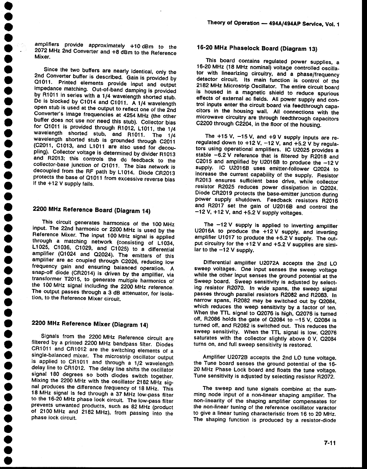
a
o
o
o
o
o
I
o
o
a
o
I
a
o
o
a
o
O
o
o
I
o
o
O
I
o
o
o
o
t
,
o
a
o
I
O
o
o
o
o
o
o
I
o
amplifiers provide approximatety
+10
dBm to the
2072
MHz
2nd
Converter
and +g dBm to the Reference
Mixer.
Sinc€
the
two buffers
are..nearly
identical,
only
the
2nd Converter
buffer
is described.
'Oain
is provicled
by
Q1011. printed elements
provide input and ortpui
imp:91199
matching..
Out-of-band
damping
is provided
by R1011
in series
with
a t/4 wavelengih
snorted
stub.
Dc is btocked
by
G1014
and
C101t. i t1+
wavetength
open
stub
is used
at
the output
to reflect
one
of
the
2;d
Converter's
image
freguencies
at 4ZS4
MHz (the
other
buffer
does
not
use
nor need
this stub). Collector
bias
for Q1011
is provided
through
Rtfiz; 11011,
the 1/4
wavelength
shorted stub. and R1011. The 114
wavetength
shorted
stub is grounded
through
C2Oi
1
(C2011,
Cl0lg, and L1011
aie also used
for decou-
pling).
Coilector
vottage
is determined
by
divider
R101g
and R2013;
this controts the dc te6dback
to the
collector-base junction
of eloll. The bias
network
is
decoupted
from
the RF path
by L1014. Diode
CR2013
protects
the
base
of el01 1
from
excessive
reverse
bias
if
the +12
V
suppty
fails.
2200 MHz Reference Board (Diagram t4)
_ Th," circuit generates
harmonics
of the 100MHz
input.
The
22nd
harmonic
or 2200
MHz
is used
by the
Reference
Mixer.
The input 100
MHz signal
ls apptieO
through
€^matching,network lconsistiig
of LiOg4,
L1025,
C1096,
C1029,
and Clb2S)
to i oinerential
amplifier (01024 and e2024). The €mitters
of this
ampfifier
are ac coupled
through C2026,
reducing
low
frequency gain and ensuring balanced
operation.
A
snap-ofr
diode (CR2014)
is driven
by the amplifier,
via
transforner
T201
5, to generate
muitipte
harmonics
of
the 100
MHz
signat
inctuding
the 22Ob
MHz
reference.
The output
passes
through
a 3 dB attenuator,
for isola-
tion,
to
the Reference
Mixer
circuit.
22A0
MHz Reference Mixer (Diagram i4)
Signals
from the 2200
MHz Reference
circuit
are
filtered
by a printed
22AO
MHz bandpass
nner. OioOei
CR1011
and
CR1012
are
the switching
elements
of a
single-balanced
mixer. The microstrip
Lscillator
output
is applied
to CR1011
and through
a 1/2 wavelength
deray rine
to
cRl012. The
deray
rine
shifti
the
osciilator
signal 180 degrees
so both diodes switch
together.
Mixing
the
2200
MHz
with the osciilator
Z1g2
Mfiz sig_
nal produces
the
difference
frequency
of 1g
MHz. This
18 MHz
signat
is fed
through
a 3Z
MHz
tow_pass
fitter
to th€ 16-20
MHz
phase
lock
circuit.
The
low-pass
filter
pley9lls llwanted products,
such
as 82 MHz (product
of 2100MHz
and 21g2
MHz),
from passing
into the
phase
lock
circuit.
Theory
of Opera{on - 4g4Ll4g4Ap
Servlce,
Vol. 1
16-20
MHz Phasetock
Board
(Diagram
13)
This board contains
regulated
pow€r supplies,
a
16-20
MHz
(18
MHz
nominal)
voltage
controlled
oscilla-
tor with linearizing
circuitry,
and a phase/frequency
detector
circuit. lts main function is control of thi
2182
MHz
Microstrip
Oscillator. Th€ entire
circuit
board
is housed in a magnetic
shield to reduce spurious
efiects
of external
ac fields. All power supply
and con-
trol inputs
enter thg circuit board via feedthrough
capa-
citors in the housing
wall. All connections
with the
1ic^loyave
circu_rlry
are through
feedthrough
capacitors
c2200
through c22a4.
in the floor
of the ho=using.
The
+15V, -lSV, and
+gV supply
inputs
are
re-
regulated
down
to +12V, -12V, and
*5.2 V by regula-
tors using operational
amplifiers.
lC U2O2S
prbvides
a
stable
-6.2 V reference
that is fittered
by R201g
and
C2015
and amptified
by U20t6B
to produte
the
-i2V
supply. fC U20168 uses emitter-foilower
e2024 to
increase
the current
capability
of the supply. Resistor
R2013
ensures sufficient
base drive, wiriie collector
resistor R2025 r€duces pow€r dissipation
in e2024.
Diode
CR2019
protects
the base-emitter
junction
during
power supply shutdown. Feedback
resistors R2016
and R2017
set the gain of U2O16B
and control
the
-12 V, +12
V, and
*5.2 V suppty
vottages.
..^-fE -12V suppty
is apptied
to inverting
amptifier
U2016A
to produce
the +12
V supply,
and inverting
amplifier
U1017
to produce
the +S.2
V suppty.
The
out-
put
circuitry
for the
+12V and
+5.2
V supplies
are
simi-
lar
to
the
-12 V
suppty.
Differential
ampliffer
V2072A
accepts
th6 2nd LO
sweep
voltages. One input
senses
the sweep
voltage
while
the other
input
senses
the
ground
potentiat
at the
Sweep
board. Sweep
sensitivity
is adjusted
by select-
ing resistor R2070. fn wide spans, the sweep signal
passes
through
parall€l
resistors
R2AE2 and R20g3.
ln
narrow spans, R2082 may be switched out by 02094,
which
reduces
the weep sensitivity
by a factor
of ten.
When
the TTL signat
to 02026 is high,
e2076 is
tumed
off,
R2086
holds
the gate
of e2094 to -lS V. e2094 is
turned
off, and
R2082
is switched
out. This
reduces
the
sweep
sensitivity.
When
the TTL signal
is low,
e2026
saturates
with the collector
stighfly
above
0 V, O20g4
turns
on, and
full
sweep
sensitivity
is restored.
Amplifier
U2072B
accepts
the 2nd
LO tune vottag€.
the Tune
board senses
the
ground
potential
of the 16-
20
MHz
Phase
Lock
board
and floats
the tune
voltage.
Tune
sensitivity
is adjusted
by selecting
resistor
R2Ol2.
The sweep and tune signals
combine
at the sum-
ming
node
input
of a non-linear
shaping
amplifier. The
non-linearity
of the shaping
amptifier
compensates
for
the non-linear
tuning
of the
reference
oscillator varactor
to give
a linear
tuning
characteristic
from 16
to 20 MHz,
The shaping
function
is produced
by a resistor-diode
7-11
Theory of Operation - 4g4ful4g4Ap Servlce, Vol. 1
afray in the feedback loop of inverting amplifier
ul073A.
All of the amptifier's
feedback
is through
R1072
when
the output swings
to the negative
limit. As th€
output voltage swings less negative,
it sequentially
passes
the tap-point
voltages
of a series of voltage
dividers
connected
b€tween
0 V (the
summing
node
at
pin 12)
and a negative
reference
s€t by e1047. lf the
ot
tput becomes
positive
with
respect
to a given
divider
tap, a corresponding
diode in U2059 forward
biases
and
connects
the output
to the
tap,
which
creates
addi-
tional feedback
through
one leg of the divider
to the
summing
node. This causes
R2051,
then R2052,
then
R2053
(as so on through
R20S6)
to be connected
in
parallel
with R1072 as the amptitier
output becomes
le$s negativs. This progressively
increases
the feed-
back,
which
causes
the
gain
of Ul073A
to decrease.
Another
series
of dividers
connected
between
the
amplifier's output and a negative
vottage reference.
causes
the diodes
in U1059
to sequ€ntlalty
conduct
as
the output becomes
more positive. Resistors
R2O6O,
then
R2061,
then R2062
(as
so on through
R206S)
are
sequentially added in parallel
with the existing
feed-
back. Soft diode turn-on
characteristics
and a large
number of breakpoints
result
in smooth
gain changes.
The nonlinear
amplifier's
voltage-gain
characteristic
is
controlled
by the shaper
reference
voltage,
which
is set
by R2049. Altering
R2049
wiil make
the breakpoints
either closer
together
or further
apart;
in practice,
this
resistor
is sel€cted
to correct
the
tolerance variations
of
th€
18 MHz
VCO
varactor.
The fomrard drop of the shaper diodes gives
Ul073A an offset voltage. Temperature
correction
diodes CR1086,
CR1087,
and CR1OBB correct
this
ofiset over a wide temperature
range by summing
a
co.rection voltage
through
R1074. These
diodes also
compensate for the lack of s€ries
diode drop across
R1072 and eliminate
offsets
at the summing
input of
Ul0738. Selecting
R1070
provides
fine adjustment
of
the
VCO's
center
frequency.
lC U107gB
is an inverting
amplifier
that increases
the shaper
output
voltage
swing
to a level
that can control
the varactor
of the 1g MHz
vco.
A differential
amplifier with weil-defined
timiting
characteristics
is used for the 1g
MHz VCo. Emitter
degeneration is Lsed
to control
loop
gain. Transistors
02096 and Q2087
form the differentiat
pair of transis-
tors, with the emitters coupled through C2091.
Transformer T2092 provides ac feedback for the
collector-base
junction
of 02096 and also creates
the
maiority
of the resonator
inductance.
The
total resona-
tor inductance may
b€ adjusted
by trying
different com-
binations
of connections
between
taps on inductor
Tl 091
and
transformer
T2092.
These
taps allow coarse
adiustment of the VCO
center
frequency.
The
capacitor
of the resonator is varactor
CR1089.
Capacitor
C10gg
7-12
complet€s the resonator ac path and acts as a dc
bloc( which
allows
a bias voltage
to be impressed
on
the varactor. Resistor R2092 and capacitor C2090
damp the 02096 collector, which prevents high-
trequency
instability in the oscillator.
Translstor
Q2087
provides
a bufiered
oscillator output.
A discrete two-stage amplifier provides an unsa-
turated voltage gain of approximat€ly
43 dB for thg
18MHz signal lrom the 22A0
MHz Reference
Mixer
board. Transistor Q1041 ls the common-emitter
first
stage while Q1042 and Q1043 form the difierential
second stage. Th€ differential stage limits the output
swing to 0.8
V to prev€nt over- driving the following
ECL circuitry. Dc bias
is malntained
by Q1041, which
has dc collsctor-base feedback via R1O46 and the
Rl043/R1048 vdtage divider. Transistor Q1043
receives its base
bias through R1042. Each
transistor
operates
with 5 mA of quiescent
current.
ECL line receivers
U2041D
and
U20418 amplify and
bufier
the
18 MHz
signals from
the Reference Mixer and
the VCO, respectively.
These two signals are then
applied to the phase/frequency
detector for com-
parison.
A pair of ECL D-type flip-flops, U2031A and
U20318,
comprise the phase/frequency
detector. The
flip-flops drive a common reset lins with a wired-AND
output. The clock input of u20318 is driven
with
the
signal from the 18MHz VCO,
and
the clock
input of
U20314
is
driven
with
the
signalfrom
the
18 MHz
signal
from
the Referenee
Mixer.
Both flip-flops are configured
to r€set together
whenever
both
are set. lf they are
clocked
with signals
that exactly match in trequency and phase,
then both
flip-flops set simultaneously and then almost immedi-
ately reset. lf the R€ference Mixer signal has a slight
phase lead, U2031A will remain set longer than
U20318. lf the Reference
Mixer signal has a slight
phase
lag,
U20318
will set
first
and
remain set the long-
est. The signal that has
the phase
lead will cause
the
associated flipflop to be set a grgater p€rcentag€
of
time than
the lagging flip-flop. lf there
is a frequency
difference between
the two inputs,
the flip-flop with
th€
higher input frequency
will
be set more of the time than
the other flip-flop, The ratio between
the filtered output
signals
of the two flip-flops
indicates whether the
Refer-
ence Mixer signal
leads,
lags; or differs
in frequency
from
the
18 MHz
VCO signal.
The outputs
of the flip-flops
are low-pass filtered by
Cl031 and C1028
and applied
to differential
amplifier
U1031. U1031
compares
the outputs
of the flip-flops
and produces
an output
that controls the tuning
of the
2182MHz microstrip
oscillator. The phase-lock
loop
bandwidth is controlled by R1026,
C1029,
Rl027,
and
C1026. The gain slope
breaks to -l2dB/octave for
frequencies
betow
16 kHz. Resistors R1033 and
R1034
o
o
o
a
I
o
o
a
o
a
o
a
o
o
o
o
o
o
o
o
a
o
o
a
o
o
O
o
a
t
a
o
o
o
O
o
o
O
o
o
o
o
o
O
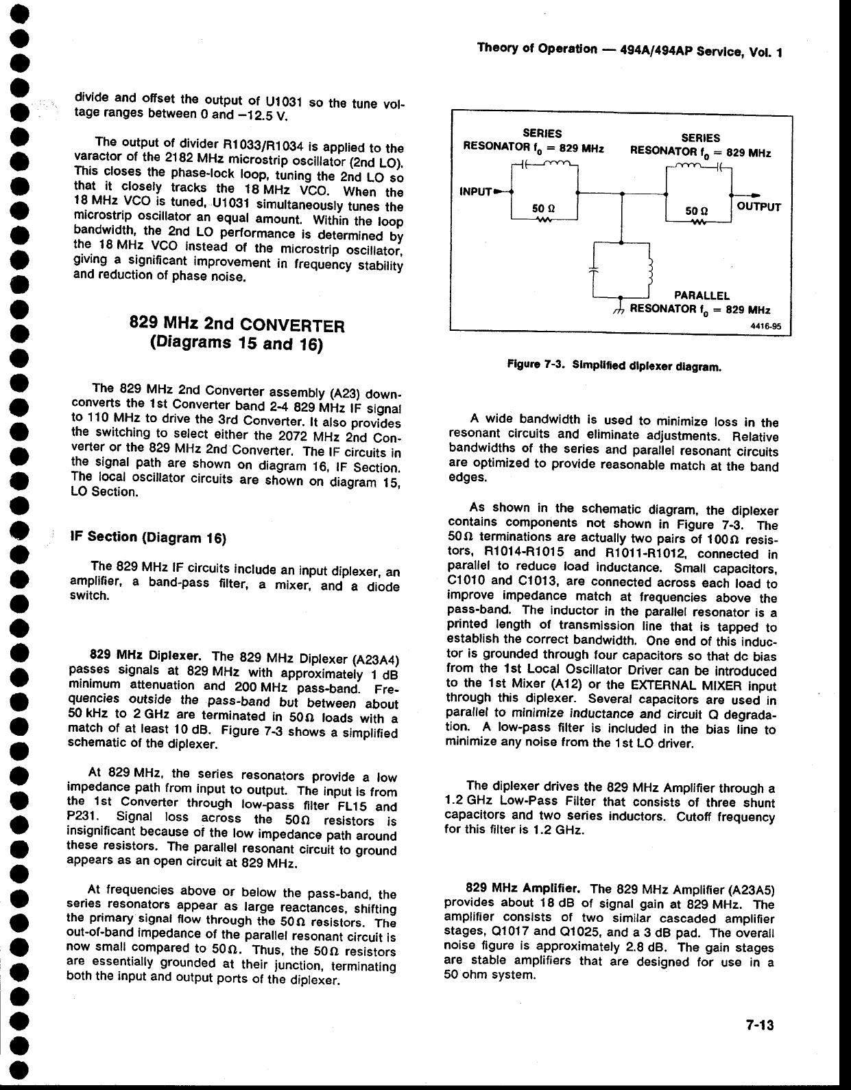
o
a
o
a
O
o
o
I
a
o
t
I
o
o
o
o
a
o
O
a
o
o
O
o
a
o
o
o
o
o
t
a
I
a
O
a
o
o
o
I
o
o
o
o
divide
and offset
lhe output
of U1031
so the
tune
vol-
tage
ranges
between
0 and
-12.5 V.
The
output
of divid-er
Rl0gg/R1Og4
is apptied
to the
varactor
of the
2192
MHz
microstrip
oscillaior
(2nd
LO).
This
closes
the phase-lock
toop,
tuning
if," ZnO
LO so
!l"l-j! 9t9JrV
tracks
the IB'MHZ
vto. when
the
18
MHz
VCO
is tuned,
Ul0gt simuttaneousty
tun€s
the
microstrip
oscillator
an equal
amount. Within
the toop
bandwidth,
the 2nd LO performance
is OeiermineO
Uy
the 18
MHz VCO instead
of the microstrip
osciilator,
giving
a significant
imprwement
in frequency
stabitity
and
reduction
of phase
noise.
829
MHz
2nd
CONVERTER
(Diagrams
15
and 16)
The
829
MHz
2nd
ConvErter
assembty
(A23)
down-
converts
the lst Converter
band
2-4
g2g
irtHz
lF signal
to 110
MHz
to drive
the
3rd Gonverter.
lt also
provides
the switching
to select
either
the 2Ot2
MAz
2nd Con-
verter
or the
829
MHz
2nd
Converter.
The
lF circuits
in
the signal
path
are shown
on diagram
16, tF Section.
The local
oscillator
circuits
are sh-own
on diagram
15,
LO
Section.
lF Section
(Diagram
16)
The
829
MHz
lF circuits
include
an
input
diplexer,
an
amplifier,
a band-pass
filter, a mixer, and a diode
switch.
Theory
of Operation
- 4g4[l4g4Ap Servtce,
Vot.
1
Flgure
7-3. Stmpllfied
dlplexer
diagram.
A wide bandwidth
is used
to minimiz€
loss in the
resonant
circuits
and eliminate
adjustments.
Relative
bandwidths
of the series
and parailel
resonant
circuits
are optimized
to provide
reasonable
match
at the band
edgEs.
As shown
in the schematic
diagram,
the diplexer
contains
components
not shown in Figure
7-3. The
50o terminations
are actually
two pairs
bt i00O resis_
tors, Rl014-R1015
and Ri011-Ri0t2, connect€d
in
parallel
to reduce
load inductance.
Small capacitors,
C1010 and C1013,
are connected
across
each
load
to
improve
impedance
match at frequencies
above the
pass-band.
The inductor
in the parallel
resonator
is a
printed l€ngth
of transmission
line that is tapped to
establish
the correct
bandwidth.
one end
of this induc-
tor is grounded
through
four
capacitors
so that
dc bias
from the lst Local
Oscillator
Driver
can be introduced
to the lst Mixer (A12)
or the EXTERNAL
MIXER
input
through
this diplexer. Severat
capacitors
are used in
paraflel
to minimize
inductance
and circuit
e degrada-
tion. A low-pass
filter is included
in the bias line to
minimize
any
noise
from
the
1st LO
driver.
The
diplexer
drives
the
829
MHz
Amptifier
through
a
1.2GHz
Low-Pass
Filter
that consists
of three shunt
capacitors
and two series
inductors.
Cutoff frequency
for
this filter is
1.2 GHz.
829 MHz Amplitier. The 829 MHz Amptifier
(A2SA5)
provides about 18 dB of signal gain at g2g MHz. The
amplifier consists of two similar cascaded amplifler
stages, Q1017
and Q1025,
and a 3 dB pad. The overall
noise figure is approximately 2.8 dB. The gain stages
are stable amplifiers that are designed for use in a
50 ohm system.
829
MHz Diptexer_.-
The 829 MHz Diptexer
(A23A4)
passes
signats
at 929
MHz with approximateiy
f Ofi
rninimum
attenuation
and 200
MHz' pass-band. Fre-
quencies outside the pass-band but betvyeen
about
50 kHz to 2 GHz are terminated
in 50O loads
with a
match
of at least
10
dB. Figure
Z-3
shows
a simplified
schematic
of the
diplexer.
At 829
MHz, the series
resonators
provide
a low
irnpedance path
from
input
to output. fnl input
is from
the 1st Converter
through low_pass
filter FL.l
5 and
P231. Signal loss across the SOO resistors is
insignificant
because
of the
low impedance
path
around
these r€sistors.
The
paraltet
resonant
circu'lt
to ground
appears
as an
open
circuit
at 929
MHz.
At frequencies
above
or below the pass-band,
the
s.eries.
r€sonators
app€ar
as large
reaciances,
shifting
the
primary
signal
flow
through
the
50O r€sistors.
The
out-of-band
impedance
of the
parallel
resonant
circuit
is
now
small
compared
to S0O. Thus,
the 50O resistors
are.
essentially
grounded
at their
junction,
terminating
both
the input
and
output
ports
of the
diplexer.
SERIES
RESONATOR
fo : 829
MHz SERIES
RESONATOR
lo = 829 MHz
500 OUTPUT
PARALLEL
RESONATOR
fo : 829 MHz
44.t695
7-13
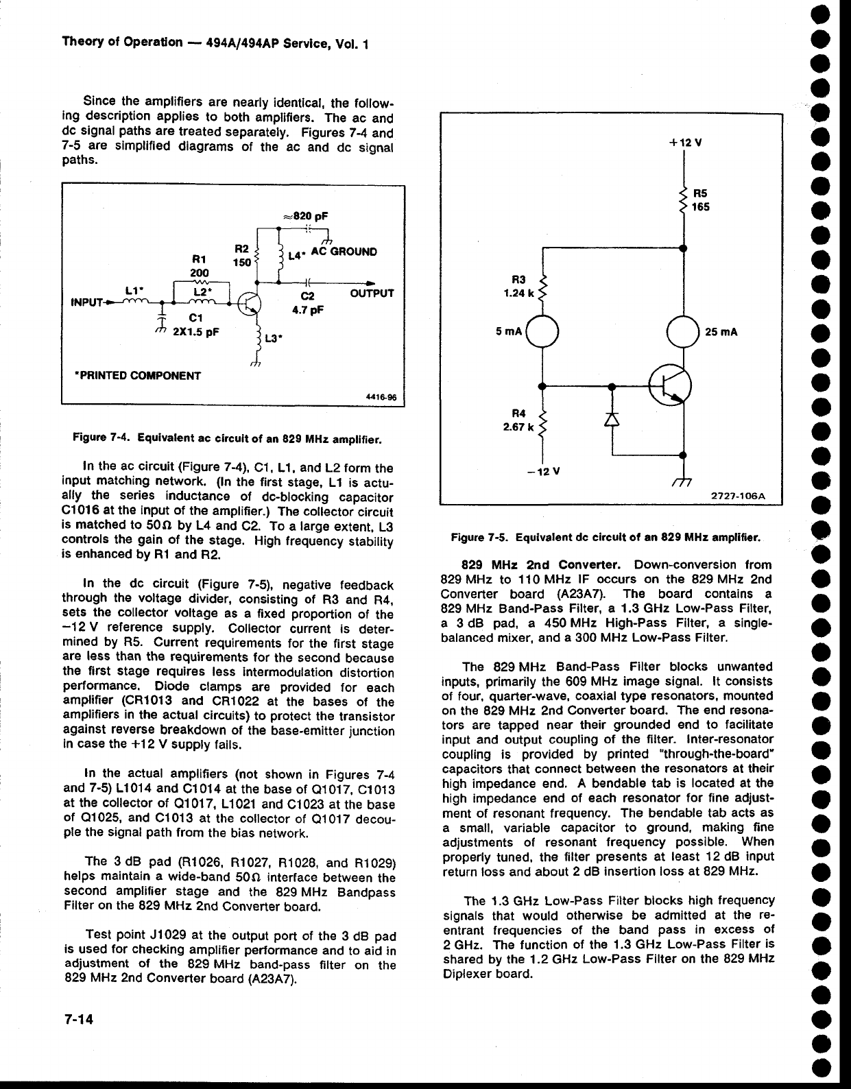
Theory of Operaton - 494A/4g4Ap
Service,
Vol. 1
Since
the amplifiers
are nearly
identical,
the follow-
ing description
applies
to both amptifiers.
The ac and
dc signal
paths
are
treated
separat€ly.
Figures
74 and
7-5 are simplified
diagrams
of the ac and dc signal
paths.
=
'PRINTED COMPONENT
Figure 7-4. Equivalent ac circuit of an B2g MH: amptifier.
f n
th€ ac circuit (Figure
7-41,
C1, L1,
and
L2 form
the
input
matching
network. (tn
the first
stag€,
L1 is actu-
ally the series inductance
of dc-blocking capacitor
cl016 at
the input of the amplifier.)
The coilector
circuit
is matched
to 50o by L4 and
c2. To a large
extent,
L3
controls
the gain
of the stage. High frequency
stability
is enhanced
by Rl and
R2.
In the dc circuit (Figure
7-5), negative feedback
through the voltage
divider,
consisting of RO
and R4,
sets the collector
voltage
as a fixed
proportion
of the
-12 V reference
supply. Collector
current is deter-
mined by R5. Current
requirements
for the first stage
are less
than the requirements
for the second
because
the first stage
requires
less intermodulation
distortion
performance. Diode clamps are provided for each
amplifier
(CR1013
and CR1022 at the bases of the
amplifiers
in
the actual
circuits)
to protect
the
transistor
against
reverse
breakdown
of the base-emitter
junction
in
case
the +12
V suppty
faits.
In the actual
amplifiers
(not shown in Figures
7-4
and 7-5)
Ll 014
and
Cl 01
4 at the
base of e1
01
7,
Cl 0.t
g
at the collector
of Q1017, L1021
and
Cl023
at
the
base
of Q'1025, and
Cl013 at the
collector
of Q1017
decou-
ple
the
signal
path
from
the
bias network.
The 3 dB pad (R1026,
R1027,
R102B,
and R1029)
helps maintain a wide-band
50O interface
between
the
second amplifier
stage and the 829 MHz Bandpass
Filter
on
the
829
MHz
2nd
Converter
board.
Test
point
J1029 at the output
port of the 3 dB pac,
is used
for checking
amplifier
performance
and
to aid
in
adjustrnent
of the 929 MHz band-pass
lilter on the
829 MHz 2nd
Converter
board
(A2347).
7-14
+12
V
2?27-1A6A
Figure 7-5. Equivalent dc circult ot an 829 MHz
amplifiee
829 MHz 2nd Converter. Down-conversion lrom
829 MHz to 110 MHz lF occurs on the 829 MHz 2nd
Converter board (A23A7). The board contains a
829
MHz
Band-Pass
Filter, a 1.3 GHz Low-Pass Filter,
a 3 dB pad, a 450
MHz High-Pass Filter, a single-
balanced mixer,
and
a 300
MHz Low-Pass
Filter.
The 829 MHz Band-Pass Filter blocks unwanted
inputs,
primarily
the 609
MHz image
signal. lt consists
of four, quarter-wave,
coaxial type resonators, mounted
on the 829 MHz 2nd
Converter
board. The
end
resona-
tors are tapped near their grounded
end to facilitate
input and output coupling
of the filter. lnter-resonator
coupling is provided by printed "through-the-board"
capacitors
that
connect b€tween
the resonators
at
their
high
impedance end. A bendable tab is located at the
high impedance end of each resonator
for fine
adjust-
ment of resonant frequency.
The bendable tab acts
as
a small, variable capacitor
to ground, making fine
adjustments of resonant
frequency possible. When
properly
tuned, the filter
presents
at least
12
dB input
return loss and
about
2
dB
insertion loss at
829 MHz.
The
1.3
GHz Low-Pass
Filter
blocks
high trequency
signals
that would otherwase
be admitted
at the re'
entrant frequencies
of the band pass in excess of
2
GHz. The function
of the
1.3 GHz Low-Pass
Filter
is
shared by the 1.2
GHz
Low-Pass
Filter on
the 829
MHz
Diplexer board.
o
o
o
o
O
a
o
a
o
a
o
a
o
o
o
o
o
o
o
o
a
o
o
o
a
o
o
o
t
o
o
o
O
o
O
o
o
o
o
a
a
o
o
o
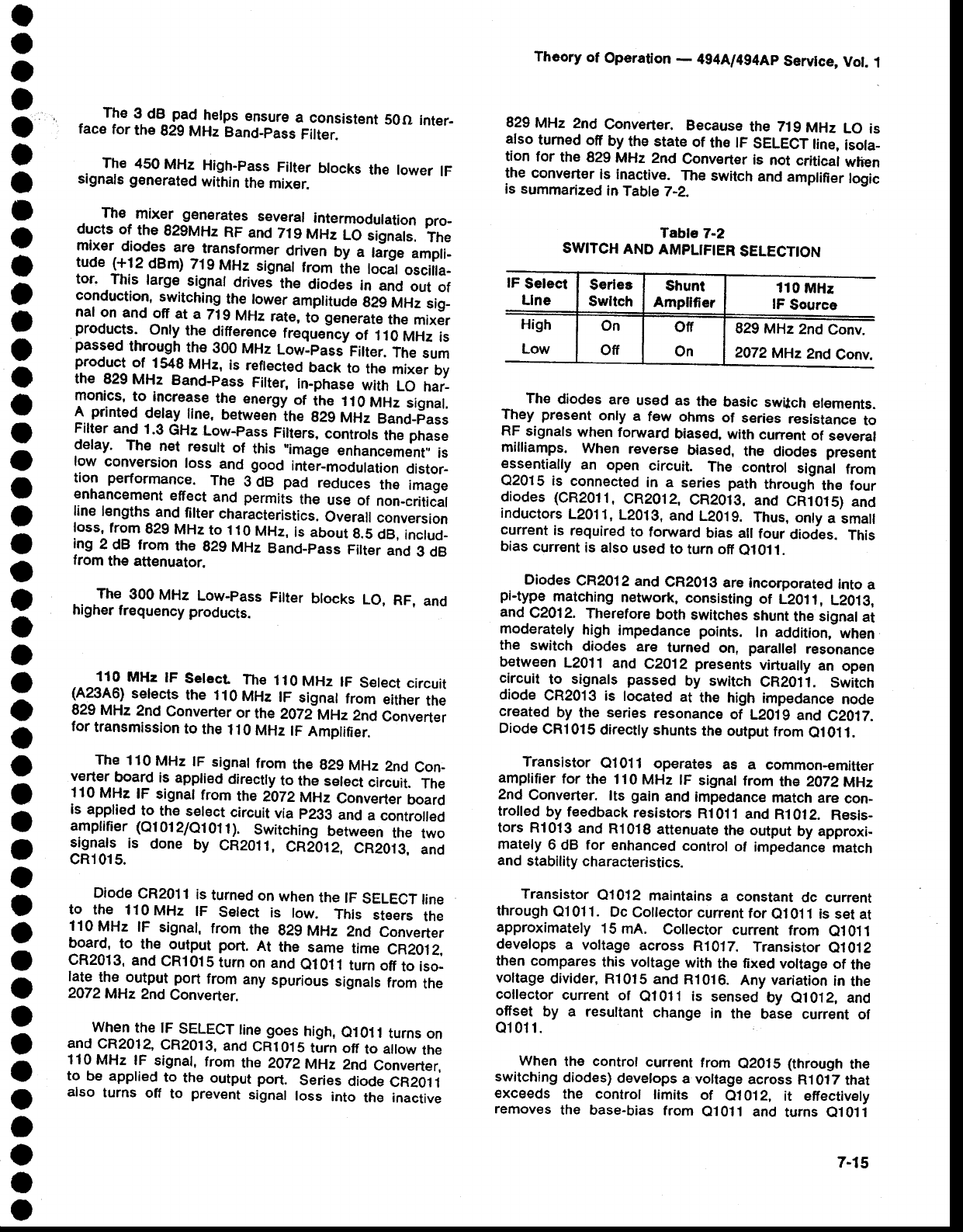
o
a
o
a
o
o
O
I
I
a
a
t
o
O
a
o
o
o
t
a
o
a
O
a
a
o
o
o
t
o
O
o
t
o
o
a
o
a
o
o
o
o
o
o
_ The
3 dB pad helps
ensure
a consistent
5Oo inter-
face
for
the
829
MHz
Band-pass
Filter.
. T!" 450
MHz High-pass
Filter
btocks
the tower
lF
signals generated
within
the
mixer.
. The mixer generates several intermodulation
pro-
ducts
of the 829MHz
RF
and
71g
MHz LO
signats.
The
mixer
diodes
are transformer
driven
Oy
a targe
ampli-
tucre
{+12dBm) 719
MHz signar
trom t'he
rocit osciita-
tor. .This large
signal
driveJ
the diodei in and out of
conduction,
switchinglhe.lower
amplitude
g29
MHz
sig_
nal
on and
off at a 71
g MHz
rate,
to generate
the
mixer
producJ:: Onty
the difference
trequeicy
of 110
MHz
is
passed
through
the
A00
MHz
Low-pasj filter. The
sum
product
of 1548
MHz,
is reflected
back
to th€
mixer
by
the 829
MHz Band-pass
Filter,
in-phase
with LO har-
monics,
to increase
the energy
of ine 110
MHz signal.
A..printed
de-lay
line,
Uetween
itre S2g
MHz Band_pass
Filter
and 1.3
GHz
Low-pass
Filters,
"ontrot"
the
phase
delay, The net rssult of this ,'image
enhancem€nt,,
is
low conversion
loss and good intJr-modulation
distor-
tion performance.
The O
dB pad reduces
the image
enhancement
effect
and permits
the use of non-critical
line
lengths
and
filter
characteristics.
Overall
conversion
loss,
from
829
MHz
to 1.10
MHz,
is
about
g.5
dB,
includ-
ing 2 dB from the 929
MHz
Band-pass
Fitter
and
g dB
from the attenuator.
The 300
MHz Low-pass
Filter btocks
LO, RF,
and
higher
frequency
products.
110
MHz
lF Select The
110
MHz
lF Select
circuit
{1?3161
selects
the 110
MHz tF signat
from either
the
829
MHz
2nd
Converter
or the 2OlZ-UAz2nd
Converter
for
transmission
to
the
110
MHz
tF
Amptifier.
The
110
MHz
tF
signat
from
the
929
MHz
2nd
Con_
y919r-boa( is apptied
direcfly
to thE select
circuit.
The
1'f 0 MHz lF signal
from
the iaZZu{z Convert€r
board
is applied
to the
select
circuit
via
p233
and
a controiled
amplifier
(Ot012/Oi011).
Switching
between
the two
lgft:_ is done by CR2011,
CRtOt2, CR2013,
and
cR1015.
Diode
CR2011
is
turned
on
when
the
tF
SELECT
line
to the 110MHz lF SElect
is low. Thls steers
the
110
MHz lF signal,
from
the g29
MHz 2nd Converter
1119:-to the_output port. At the same
time CR2012,
CR2013,
and
CR't01S
turn
on
and
el011 turn
off
to iso-
lalg_the
output
port
from
any
spurious
signals
from
the
2072
MHz 2nd
Converter.
When
the lF
SELECT
tine
goes
high,
etOtl turns
on
and
CR2012,
CR201g,
and
CBl01S
tirn otr
to ailow
the
110
MHz
lF signal,
from
the 2O72MHz
2nd
Converter,
to be apptied
to the output port. Series
diode
CR2011
also turns off to prevent
signal
loss into th€ inactive
Theory
of Operation
- 4g4[l4g4Ap SeMce, Vot.
1
829
MHz 2nd Converter.
Because
the 7l
g MHz LO is
also
turned
off
by
the state
of the
lF sELECT
line,
isola_
tion for the 829 MHz 2nd Converter
is nol critical
wlien
the
converter
is inactive.
The
switch
and
amplifier
logic
is summarized
in
Table
Z-2.
Tabte
Z-2
SWITCH
AND
AMPLIFIER
SELECTION
lF Select
Llne Serles
Swltch Shunt
Ampllfier 110
MHz
lF Source
High
Low
On
otr otr
On
829 MHz
2nd
Conv.
2O72MHz
2nd Conv.
The diodes
are used
as the basic
switch
el€ments.
They present
only a few ohms
of series
resistance
to
RF
signals
when fonrvard
biased,
with
current
of several
milliamps. When reverse
biased,
the diodEs
present
€s_sentially
an open circuit. The control signal from
0201
5 is connected
in a series
path
through
the four
diodes (CR2011,
CR2012,
CR201g,
anO
CAtOtSl
anC
inductors
L2011,
L2019,
and
L2019.
Thus,
only
a small
current
is required
to fonarard
bias all
four
diodes. This
bias
current
is also
used
to turn off
el01 1.
Diodes
CR2012
and
CR2013
are
incorporat€d
into
a
pi+!pj_
matching
network,
consisting
of L2011,
L2O1O,
and
C2012.
Therefore
both switches
shunt
the signal
at
moderately
high impedance points. In addition,
when
the switch diodes are turned on, parallel
resonance
between
L2011
and CzAl2 presents
virtually
an open
circuit to signals passed by switch CR2O11.
Switch
diode CR2013 is tocated
at th€ high impedance
node
created
by the series
resonance
of L2019
and C2017.
Diode
CRl015
direcily
shunts
the output
from
el01
l.
Transistor
Q101
1 operates
as a common-ernitter
ampfifier
for the 110
MHz tF signat
from
the 20Z2MHz
2nd
Converter.
lts gain
and
impedance
match
are
con-
trolled
by feedback
resistors
R101i
and
Rl012. Resis-
tors R1013
and R1018
attenuate
the
output
by approxi-
mately
6 dB for enhanced
control
of impedance
match
and
stability
characteristics.
Transistor
Q1012
maintains
a constant
dc current
through
01011.
Dc
Coilector current
for
01011 is
set at
approximately
15
mA. Collector
current
from e1011
develops
a voltage
across
Rl017. Transistor
el012
then compares
this voltage
with
the
fixed
voltage
of the
voltage
divider, Rl015
and
R1016.
Any variation
in
the
collector
current of Ql 01
1 is sensed
by e101
2, and
ofiset by a resultant
change
in the base curent of
Q1011
When
th€ control
current
from e2015 (through
the
switching
diodes)
develops
a voltage
across
Rl017 that
exceeds the control limits of 01 01 2, it effectively
removes
the base-bias
from e101 i and turns el 01 I
7-15
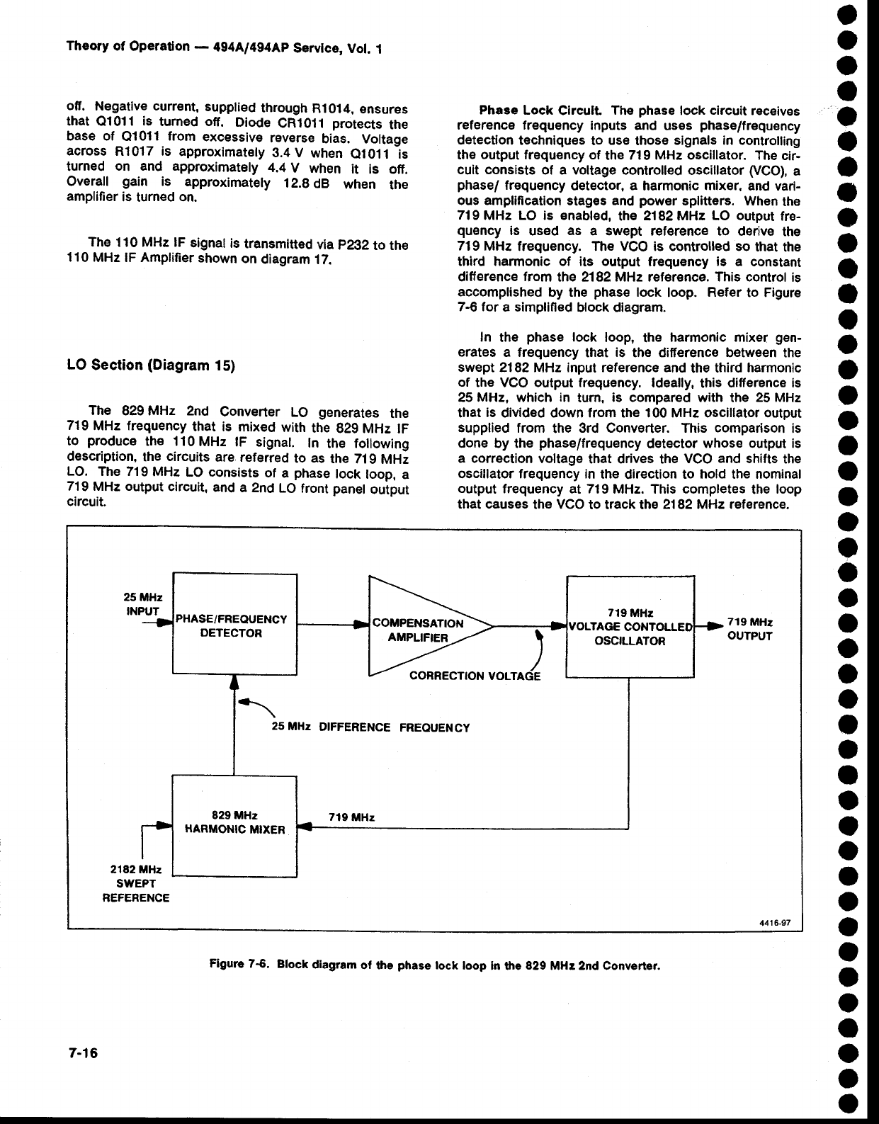
Theory
of Opera$on
- 4944/4g4Ap
Servtce,
Vol. I
off. Negative current.
supplied
through
Rl014,
€nsures
that Q1011 is turned off. Diode
CRt011 protects
the
base of 0101 1 from excessive
reverse
bias. Voltage
across
R1017 is approximately
9.4 V when
e1011 ls
turned on and approximately
4.4V when it is off.
Overall gain is approximately
12.9
dB when the
amplilier
is turned
on.
The
110 MHz lF signal
is
transmitted
via
p2g2
to the
110
MHz lF Amplifier
shown
on
diagram
17.
LO Section
(Diagram'15)
The 829 MHz 2nd Converter LO generates
the
719
MHz frequency
that is mixed
with
the 929 MHz tF
to produce
th€ 110MHz lF signat. ln the following
description,
the
circuits
are referred
to as the 71
g MHz
LO. The 719MHz
LO consists
of a phase
lock
loop,
a
719 MHz output
circuit,
and
a 2nd
LO front paneloutput
circuit.
Phase
Lock
Circult The
phase
lock
circuit
receives
reference frequency
inputs
and uses phase/frequency
detection
techniques
to use
those
signals in controlling
the
output
frequency of the
719 MHz oscillator. The
cir-
cuit consists of a voltage
controlled oscillator (VCO),
a
phase/
frequency
detector,
a harmonic
mixer,
and vari-
ous amplification
stag€s
and
power
splitters.
When
the
719
MHz LO is enabled,
the 2182MHz
LO output
fr€-
quency is used as a swept r€f€rence to d€rive
the
719 MHz frequency. The VCO is controlled so that the
third harmonic of its output frequency is a constant
difference
from the 2182MHz reference. This control
is
accomplished
by the phase
lock loop. Refer
to Figure
7-6 for a simplified
block diagram.
In the phase lock loop, the harmonic
mixer gen-
erates
a frequency
that is the difierence between
the
swept 2182
MHz input reference and
the third harmonic
of the VGO
output frequency.
ldeally,
this difference is
25 MH4 which in tum. is compared
with the 25
MHz
that
is divided down from the 100 MHz oscillator output
supplied
from the 3rd Converter. This comparison
is
done by the phase/frequency
det€ctor
whose output is
a correction
voltage
that drives the
VCO
and shifts
the
oscillator frequency in the direction
to hold the nominal
output
frequency at 719
MHz. This completes
the loop
that
causes the vco to track the
2182 MHz reference.
t
t
o
a
o
o
a
I
o
o
o
o
o
o
O
O
o
o
o
O
o
o
o
o
o
o
o
o
a
a
a
o
o
o
I
o
o
o
o
o
a
O
a
o
PHASE/FREOUENCY
DETECTOR COMPENSATION
AMPLIFIER OSCILLATOR
25
MHz DIFFERENCE
FREOUENCY
829 MHz
HARMONIC
MIXER
7-16
Figure
7$. Block
diagram
of the phase
tock
loop
in the
829
MHe 2nd Converter.
o
a
o
I
o
I
t
t
o
o
I
t
o
o
o
o
o
t
o
a
o
o
o
O
a
o
o
o
t
a
o
a
t
o
a
o
I
o
a
o
o
a
o
o
Because
the
grd harmonic
of 719
MHz is locked
to
the 2182MHz reference,
the tuning range ot tne
719
MHz
osciilator
is onty
one
third
oithe tuning
range
of the reference.
Since.th:
rgnge
is
4 MHz,
ttre
ringe-ot
the
719
MHz
osciilator
is 71g
Jt.gg trlnz.
'
The 719
MHz VCO (O20i4) uses a Cotpitts
configuration,
with a printed
circuit quarter-wavelength
transmission
line resonator,
to achieve
high specir"t
purity
and
good
thermat
stability.
Correction
voliage
is
applied
to varactor
ctiode
CRldlt (which
is connected
at the midpoint
of the transmission
line resonator)
to
vary ths r€sonant
frequency
of the transmission
jine
ov€r a 1.5
MHz
range.
A tunable
transmission
line
(atso
printed)
adjacent
to the printed
resonator
compensates
for variations
in component
tolerances
and resonator
dimensions-
This
adjustable
transmission
line
is cut,
at
factory
calibration,
to the correct length
for proper
VGO
operation.
A scale
with
minor
divisions
every
iMHz is
printed
next
to th€ adjustabre
line
to aid in caribration.
The
output
from
the oscillator
is extract€d
near
one
end
of the quarter-wavelength
line through two printed
inductors
and applied
to output amplitiers
through
a
power
splitter.
The
719MHz
VCO
is enabted
or disabted,
under
microprocessor
control,
dependent
upon
the frequency
band.
being anatyzed,
by
the
tF
SELECT
line. When
this
lin€ is low, e201 7 is cut off, which turns e201
6 otr.
This, in turn, cuts off transistor
e8015 (which
is the
current source for oscillator
transistor
e20t+;, tnus
disabling
the
719
MHz
oscillator.
From
the oscillator,
the *6 dBm 719
MHz output
signal
is applied,
throu-gh
a power
divider
consisting
of
resistors
Rl021, Rl022, and Rl02O, to tsolation
amplifier
Q1021. From the other side of this power
9iut9gr,
the signat
is apptied
to an output amptifier
(02021)
for transmission
to the 929 MHz
2nd
Converter
Mixer circuit. A second isolation
amplifier
(OgO21),
Il.e^n!i911
in
configuration,
provides
isotation
between
the
719
MHz
oscillator
output
and
any
undesired
Harmonic
Mixer
products.
The
829 MHz
Harmonic
Mixer
produces
not
only
the
required
25MHz
difference
frequency,
but also many
higher
order intermodulation
proOucts.
Two of these
frequencies,
744
MHz and 6g4
MHz, are 25
MHz
from
the 719
MHz oscillator frequency. The isolation
amplifiers,
01021
and
e3021,
provid6
sufficient
attenua_
tion in the reverse
direction
to prevent
these
products
from getting
into
the 829 MHz
mixer
to produie spuri_
ous
signals.
To provide
maximum
reverse
attenuation
in each
amplifier
circuit,
external
RF feedback
is kept to a
m,inimum.
An output
matching
LC network,
consisting
of capacitor
C1025
plus
a printed
inductor
for
e1021,
and
capacitor
C3021
plus
a printed
inductor
for e3021,
presents
an
optimum
load
impedance
to the collector
of
Theory
of Operation
- 4g4ful4g4Ap
Servlce,
Vol. 1
each
transistor
to allow
maximum
power
transfer
to the
attenuator
that precedes
the harmonic
mixer. An input
LC matching
network consisting
of capacitors
Ct0'23,
919?,plus a printed
inductor
for al02i and
capacitors
C3023,
CgA22,
ptus
a printed
inductor
for e302i, estab_
lishes
the
50 ohm
input
impedance
to each
transistor.
A 3 dB attenuator
consisting
of resistors
R3021,
R3022, R2021,
and R3023, at the output of isoiation
amplifier Q3021, provides a non- rehective
source
impedance
to the mixer. Without
the attenuator.
mixer
conversion
loss
could
vary
from
unit
to unit.
The 829
MHz Harmonic
Mixer,
consisting
of diode
CR2021,
inductor L2A14,
and a half-wavelength
(at
2182
MHzl transrnission
line, produces thE difference
frequency
between
the third harmonic
of the 719
MHz
9:9,11?tol
frequency (nominalty
2157
MHz) and the
2182
MHz reference frequency. Note that the
2182MHz sfgnal
is supplied
trom tfre 21g2MHz
2nd
Local
Oscillator
through
coaxial
connector
p237
and
the
power divider,
consisting
of resistors
R1021,
R1029,
and
R1022.
to a 112
wavelength
transmission
line. The
VCO input
to the mixer switchEs
diode CR2021
at a
719
MHz
rate, The
2182MHz
reference
acts
as
the
RF
and is applied
to the diode
from the
transmission
line.
The resultant 25
MHz int€rmediate frequency is
diplexed
from
the mixer
through
th€ 1OO
MHz tow-pass
filter
consisting
of capacitor
C3014
and inductor
L{jfi4.
(Diode
CR2021 is mounted
on printed
circuit
board
cut_
outs to relieve any nec€ssity
of bending
the diode
leads. Lead bending
may fracture the diode case.)
fnductor
L2014
provides
a bias
return
path
to allow
the
diode
to switch
at a 719
MHz rate.
From the 829 MHz Harmonic
Mixer, the signal
is
applied
through
the above
mentioned
low-pass
filter
to
cascaded amplifiers Ul053 and Ui0448. These
amplifiers
boost
the €2 dBm mixer
output
signal
to a
level appropriate
to drive
the phase/frequency
detector.
lC amplifier
(U1053)
contains
two differential
amplifiers
in cascade; amplifier
lC U1044 contains only one
differential amplifier
and acts as a bufier. When
the
loop is first acquiring
lock, such as at power-on,
the
nominal
25
MHz lF may be as high
as 34 MHz. Two
stages
of amplification
are
necessary
to ensure
enough
gain tor the phase/frequency
detector
to drive
the lF
back
to 25
MHz;
the
buffer is necessary
to provide
ECL
levels
to the
detector.
The
second
input
to ths phase/frequency
detector
is
the 100
MHz signal,
from
the reference
oscillator
in
the
3rd Converter,
via two amptifier
stag€s,
U1022A
and
U10228, and a divide-by-four
circuit, U1036A
and
U10368. The 100MHz signat
is divided
down
to a
25
MHz reference for application to the
phase/frequency
detector.
Two stages
of amplification
are
used
to isolate
the 100
MHz
reference
bus
from
sig-
nals
generated
in the
local
oscillator
section
of the 2nd
Converter. This
stable
25
MHz reference
signal
is used
7-17
Theory of Operaton - 4g4A/4g4Ap
Service,
Vol.
1
to lock the difference
trequency
from th€ Harmonic
Mixer
to 25
MHz.
The phase/frequency
detector output
is a voltage
that is proportional
to the
phase
difierence
between
the
25
MHz refer€nce
and the lF signal from
the g29
MHz
Harmonic
Mixer. This
correction
voltage
is
then applied
to the
719
MHz
VCO
to lock
it to the
reference.
The detector
circuit consists
of two D-type
flip-flops,
U2U7A and U2047B,
and a differentiat
ariiptifiei
stage
used
as
a NAND-gate
(U1044A).
The 25
MHz
referenie
signal, from the frequency
divider, is apptied
to the
cfock input
of flip-flop
U204tA;
the
nominat
25
MHz
sig-
nal
from
the
829
MHz Harmonic
Mixer is applied
to the
clock input
of flip-flop
V204ZB.
The
rising
€dg€
of the
input
signal
to each
flip-flop
causes
the e(bar)
outputs
to return to the low level only after both flip-flops
have
been
clocked.
lf the
frequency
out
of the g2g
MHz Harmonic
Mixer
is below 25 MHz,
or if its phase
lags
that of the 25
MHz
reference,
the Q(bar)
output of ftip-flop
U2047A
witl
remain
high
longer
than
the a (ba0
output
ot u20478.
lf the frequency
out of the Harmonic
Mixer is above
25 MHz,
or if its phase
leads,
the opposite
will occur.
When the two flip-flops
are clocked
at the same
fre-
quency
and
phase,
the two outputs
will be high
for the
sam€
amount
of time. The e(bar)
outputs
are
applied
to a compensation
or differential
amplifier
U3059,
that
determines which
output
is high
for
the
longer
time.
Compensation
amplifier
Ug05g
provides
part
of the
loop gain to ensure that the 719 MHz oscillator
will
track the sweep
of the 2192
MHz reference
oscillator.
The compensation amplifier also limits the loop
bandwidth to 100
kHz
to make
certain
that the loop
wilf
not oscillate.
Note
the
differential
inputs
to the
amplifier
each include
a low-pass RC filter to attenuate
the
undesired high frequency clock pulses from the
phase/frequency
detector.
The nominal swing of the U3053 output is from
+12V to -12V. Since the compensation
amptifier
is
capable of considerably
more output than is needed
to
control
the oscillator,
a voltage
divider is used
to limit
the output
and reduce amplifier related
noise. This
vol-
tage divider, consisting
of resistors R2053, R2054,
R3051, and
R3052, reduces
the
possible
*12V swing
to +5 V to +12 V, as reguired by varactor diode
CR1011. Nominalvoltage
swing in a locked condition
is
+6.75 to +7.5 V. Thus, dependent
upon whether the
Harmonic
Mixer
frequency
is above or below 25
MHz,
the correction voltage swing,
applied
to diode CR1011,
is more than nominal
to correct
the oscillator
frequency.
2nd Local Oscillator Oupuf Circult A portion of
each
2nd
LO
output signal is sent to the
front panel
2nd
LO OUT connector. This output provides
signal for
external
accessory
equipment,
such
as a tracking
gen-
erator. Each
local oseillator
(719
MHz and 2182 MHz)
output is applied through power dividers to a power
combiner
for application
to th€
2nd LO
OUT
connector.
The 719 MHz
oscillator
frequency
is applied
from a
power
splitter
(R3027,
R3028, R3029)
through
a 1
GHz
fow-pass filter
(C3025,
C2024, C1023. C1021
, and
three
printed inductors),
to the power combiner (R2024,
R2025,
R2026),
and the front panel 2nd LO OUTPUT.
The 2182 MHz oscillator signal is applied
through a
power
splitter
(R1021,
R1022, R1023), a 2.2
GHz
band-
pass
filter
(consisting
of coupled
1/4 wavelength
printed
lines)
to the power divider (R2024,
R2025, R2026)
and
the front
panel
2nd LO OUTPUT.
Both 2nd local oscillator signals,
2182MHz
and
719MHz, are present at the front panel when the
829
MHz
2nd
Converter
is selected.
719 MHz
Output Clrcult The 719 MHz 2nd Local
Oscillator signal is applied is applied
through divider
resistors R2021, R2023, and R2A24 to isolation
amplilier
Q2021. 02021 boosts th€ signal level from
about
0 dBm
to +12
dBm to drive the 829
MHz mixer.
The output
of the amplifier includes a 3 dB attenuator
(consisting
of resistors
R2027, R2028,
and R2029),
to
ensur€ a 50
ohms non-r€flective
source impedance.
The signal level at test
point J2026
is
typically
-6 dBm.
o
o
o
o
t
a
t
a
o
a
o
I
o
o
o
O
o
o
o
o
a
a
o
o
o
o
o
O
t
,
a
O
o
o
o
o
a
a
o
o
a
o
o
o
7-18

o
o
o
t
o
o
o
I
o
O
o
I
o
o
a
o
o
a
t
o
o
o
o
o
o
o
a
o
I
o
I
o
t
o
o
o
o
I
o
o
I
o
t
a
Theory
of Operation
_ 4g4Al4g4Ap
Service,
Vol. 1
3RD
CONVERTER
(Diagram
4)
The
1t0MHz tF Amptifier
(A32)
and
3rd Converter
(A34)
down converts
the ttO MHz ouiput
signat
from
the
2nd
Converter
to 10
MHz
for the
VariaUie
Resolution
circuits. A 100
MHz crystat
controlled
oscillator
pro-
vides.the
third
LO signal.
This
oscillator
is
phase
locked
to either
a precise
internal
10MHz reference
or an
external
1,
Z,
5, or 10
MHz
reference.
The
100
MHz
LO
signar
is applied
to the mixer
and
is oistriouteo
through
output
amplifiers
to many
other
circuits
throughout
t6e
instrument
as a reference
signal.
The
100
MFz signal
and
its harmonics
are also
available
for external
use
at
the front-panel
CAL OUT
connector
for irequency
anO
100
MHz
amplitude
calibration.
.
The 110
MHz signal is amplified
in a three_stage
gain
btock
and
apptied
through
a band_pais
fitter
and
a
low-pass
fitter. From the toiv_pass
fil6r, the signal
is
applied
to the converter,
which
consists
of a mixer,
an
oscillator,
and
various
output
amplifiers.
110
MHz
tF
AMpLtFtER
(Diagram
17)
-lnitial gain for the analyzer
is provided by the
110
MHz lF Amplifier. Thi; gain compensates
for
conversion
losses
in the thre€
mixers.
Typical
gain
for
the amptifier
is 2t dB. The amplifie,
"onjirts of three
stages
of amplification
and
an attenuator.
The
first
two
mixers
in the RF syst€m
ofier no high_frequency
gain;
therefore,
it is important
that this ariptifiei
exhibit
low
noise characteristics.
lt must atso be relatively
free
from
third-order
intermodulation
distortion.
. Signal
input
is applied
through
an
impedance
rnatch-
ing
b.and-pass
fitter
(L2044
anO
CSZS)
to'a
parailel
tuned
circuit. The
signal
is injected
into
the
paraltet-tuned
cir_
cuit
through
a tap in the inductor
and
taken
out at the
high
impedance
side
through
variable
capacitor
f;2A47.
Inductive input provides for "onu"riion to high
impedance
within
the tuned
circuit;
the extra capacltor
on the output provides
for conversion
back
to 50 ohms
l.Iil_"]:_I!: pr'.m."ry.
tuning capacitor,
C325, adjusts
tn€ resonant
point; the output capacitor, C20C7,
is
adjust€d
in combination
with
bSZS
t6r good
impedance
match
at 110MHz. This is done
wiih a return
loss
bridge. The
nominal
return
loss
is 35
dB. The
e of the
input
filter
is approximately
20.
- From
the input
fitter,
the signat
is applied
to e4053,
which is the first stage of impliRcaiion. This is a
broad-band
feedback
amplifier
to provide
good input
and output impedance
and controlied
gain. All feed-
919! is through reactive componenti (transformer
T3054),
not
resistive
cornponents.
Thus,
the
impedance
and gain can be controlled
without
significant
noise
problems.
.. The second amplifier
stage, e40g7, is essentially
the same
as the first,
with
oniy minor
bias
differences.
Gain through
each of these itages is approximately
9
dB. The
output
is applied
through
a 3 dB attenuator,
to..preserve
the impedance
figure,
to the bridged
.T;
adjustable
attenuator.
The
3 dB attenuator
consists
of
resistors
R2039,
R2038,
and
R2043.
From
the 3 dB attenuator,
the signal
is capacitively
goupled
through C2Ogl
to the aOyustabte
attenuator.
This attenuator
uses two ptN diodes, CR3030
and
CR1029,
in the mode
when
the resistance
to RF
signal
lolv is c_ontrolled
by the current
through
the diodes.
Refer
to Figure
T-7
to aid
in understandirig
tt e foflowing
description.
f f resistor
R1 in Figure
7-T
were
set
to infinite
resis_
tance
and resistor
R2 were
set to zero resistance,
the
RF signal path
would
be through
R2
to ground,
to pro-
duce infinite
signal
attenuation.
lf resistor
Rl were
set
to zero resistance
and resistor
R2 were set to infinite
resistance,
the RF signal path
would be through
Rl to
th€ load,
to produce
almost
no attenuation.
This,
basi-
cally,
is.how
the adjustable
attenuator
operates,
except
that resistors
R1 and RZ are actually
plN diodes
and
the RF path resistance
through
theie diodes
is con-
trolled
by the current
through
the diodes
in an inverse
proportion
(higher
current
results
in less resistance
to
RF).
Figute 7-7. Bridged 'T' attenuator equlvalent clrcuit
Resistors R3035 and R20gO on the detail€d
schematic
diagram establish a constant current of
approximately
2 mA from
the
15
V supply
to the diodes.
This
current
is divided
according
to the bias
on the
diodes.
The
bias, in
turn,
is established
by
gain
adjust-
ment
R1015,
from
the
+15
V suppty.
lf Rl015 is set
low
(near
ground),
diode
CR30g0
is reverse
biased
and
the
2 mA flows
through
diode
CR1
029. This routes
the RF
signaf
through
resistors
R2092
and R3029
and capaci_
tor C2029, with the impedance characteristics
of
7-1
9
Theory
of Operaton - 494A/4gdAp
Service,
Vot.
1
CRl029
added
for maximum
attenuation.
lf Rl01
5 is set higher
(nearer
+i 5
V),
diode
CR3030
is forward biased and starts to conduct. Since the
2 mA supply
current
is relatively
constant,
this subtracts
from
the current
through
CRl02g. Thus,
the impedance
of the diodes is relatively
constant,
which
results
in a
good impedance
match over a broad range. The RF
signal path is determined
by the exact amount
of
curent through
CR3030;
part of the RF signal
path
is
through CR3030
to th€ output amptifier
ind part is
through R2032 and diode CRlO2g to ground. This
results
in reduced
signal
attenuation.
lf R1015
is set to the
positive
timit,
the entire
2 mA
flows through CR3030. This routes the RF signal
through CR3030 (which exhibits titil€ resistance
with
high current)
to the output amplifier
with almost no
att€nuation.
Cl-he
insertion
loss is
approximately
I dB.)
_From
the adiustable
attenuator,
the
signal
is applied
to the linal
amplifier
09018. This
stage
ts a broad'-6and
feedback
amplifier
that supplies
relatively
substantial
output
current
and
exhibits
good
intermodulation
distor_
tion
performance.
This
is provided
primarily
through
the
large curr^ent
.capacity,
by negative
feedback
thiough
resistor
R3014,
and
emitter
degeneration
through
resls-
tor R4029. These
resistors
are sized
to provide
a r€a-
sonably good impedance
match
at 110
MHz. Nominal
gain
of the
stage
is 13
dB.
With Gain potentiomet€r
Ri0i5 set for maximum
gain (least
attenuation),
the gain of the 110MHz
tF
Amplifier
is approximatety
26dB to 27d8. R.t01S
is
normally
adjusted
for
total
gain
of 21
dB.
Th€
output
signal
from
the
110
MHz
tF
Amplifier
is
applied
through
the 110
MHz
band-pass
fitter
FL36
and
low-pass
filter
FL37
to the
3rd Converter.
110
MHz
FTLTERS
(Diagram
17)
The 110
MHz
band-pass
fitter
(FLg6)
determin€s
the
widest
resolution
bandwidth
of the analyzer,
provides
i-I1g-g-
rejection to prevent the mixer fiom producing
10
MHz
outputs
from
input
signals
of 90 MHz,
and
also
limits
the
noise
spectrum
that appears
at th€
1O
MHz
lF
circuits. The low-pass
filter
(FL3Z)
that follows
turther
reduces
harmonics
and
spurs from
the 2nd
Converters.
Both filters
are
sealed
units
with
no internal
servicing.
The
band-pass
filter
consists
of four helical
resona-
tors that are tuned
with multi-turn
trimmer
capacitors.
For purposes
of impedance
matching,
the fittei
is sym_
metrical.
Adjustment
of the filter for minimurn
attenuation
is
performed
by setting
the trimmer
capacitors.
Insertion
loss is approximately
4 dB to 4.5
dB. From
this filter.
the 110 MHz signal
is applied
to the separate
low-pass
filter. There is no adjustment for the low-pass filter.
The signal
then
feeds
the 3rd
Converter
board.
3rd
CONVERTER
(Diagram
17)
The 3rd Gonverter consists of a 100
MHz crystat
oscillator
and a mixer. lt outputs
th€ 3rd lF of 10
MHz,
for the Variable
Resolution
(VR)
circuits, and a stable
100
MHz reference
for other circuits
within
th€ instru-
ment.
100
MHz Oscillator
A Colpitts
oscillator
is formed by Q2038,
yg03g,
L1041,
C1038, and related compon€nts.
Y3038
is a
100
MHz crystal that op€rates in a series resonant
mode in
the
fEedback
loop
of the
oscillator.
The oscilla-
tor output couples through C2042 to differential
amplitier
4204402441. The two separate
outputs
of
approximately
2V peak-to-peak
amplitude
go to three
hybrids
(mixer
U3051,
distribution
amplifier
U30il1. and
cafibrator
U2022) on the 3rd Converter
board.
lnductor
L3041,
varactor diode CR3039, and crystal
Y3038
form a series resonator
that tunes th€ oscillator
approximately
*1 kHz. The RPL VOLTS
TUNE tine
varies
from 0V to +12V, changing
CR3039's
capacL
tance
to phase
lock
the oscillator
to the
Reference
Lock
source. RPL
GND is tied to ground
in the Reference
Lock module.
Mixer
At mixEr
U3051, 100 MHz enters
on pin 2 and is
amplified
to drive
a ring diode
mixer. 110 MHz enters
on pin
10 and
is mixed with
the
100 MHz
to yield
mixing
products
at 10
MHz and 90
MHz. The 1O MHz signal
pass€s
through a low-pass
filter
and
is sent
to the
Vari-
able Resolution Input circuat,
while the unwanted
90 MHz signal
is terminated
within the mixer,
Distribution Amplilier
U3031 distributes
a 100
MHz signal to other
modules
in the instrument.
The input
level on pin 2 is
typically
2 V peak-to-peak,
while the output level is
0 dBm into a 50
ohm
load.
o
o
o
o
o
o
a
o
o
t
o
a
o
o
O
o
a
a
o
o
o
a
o
o
o
o
o
o
t
o
a
o
a
o
I
o
o
a
o
o
o
o
o
o
7-20
a
o
o
I
o
I
o
I
o
o
o
I
o
o
o
O
a
a
o
o
o
O
o
o
o
o
a
o
I
o
a
o
I
a
O
o
o
o
a
o
I
a
I
a
Calibrator
u2022
and related
components
regulat€
a 100
MHz
signat
to -20dBm for the
front-panet
ill bUf connec_
tor. VRI
0S1
serves
as an aecurate
6.2
V reference,
which
is divided
to approximately
1.e
V anO
applied
to
pin
6 of U2022.
The
exact
tevet
ii set
by
R1041
the
Cal
Level
adjustmsnt.
The 100
MHz signal_
enters pin 1 and passes
through
a pin diode
variable
attenuator.
The signal
is
th€n amptified
and
passed
through
a low-pass
fitter
to
remove
any
harmonics.
The
signal
then
enters
a peak
detector-
and comparator
wnere the peak amplitude
of
the 100
MHz
signal
is compared
to the 1.2
V reference
on pin 6. An operational
amplifier
then adiusts the
att€nuation
level
of the
pin
dlode
to maintain
a constant
signat
level.
The
outqq of this
operationai
ampliRer
can
be measured
on Tp301l. A small fortion of the
1^0-0
MHz signal is attenuated tnrou'gh RzO.ll to
-20dBm. R1021
and R1022
suppfy
Uia-s-current
to the
p€ak detector
circuits. fne vottale on pins 7 and g
should
typicaily
be +5 V.
c2023, C2011,
and related components
form a
high-pass
filter
to allow
harmonics
of iOO
Mn. to pass
through
to the
front
panet.
The
nna resutt
is a calibra-
tor signal
rich
in harmonics
with an accurate
100
MHz
amplitude.
In Option
0Z instrum€nts,
the CAL
OUT
signal
goes
thr:ugh a set
of-relay
switches.
tn 50O moOe,
the out_
put goes straight
to the CAL OUT
connector. In the
750.mode,
the output
is routed
through
a 50O_to-ZsO
matching pad
and
the
output
is +ZO
Og-mV.
REFERENCE
LOCK
(Diagram
S0)
The Reference
Lock module (A36)
consists of a
".tlblg 10
MHz crystat osciilator
'(A3erc), reference
detector, frequency .synchronizer,
phaie/frequency
detector,
and
tune
window
detector. Eittrer
tne
internal
10
MHz
reference
or an
external
1,2,5,
or 10
MHz
refer-
ence
frequency
is routed
through
the
reference
detector
1o-^tlg -frequency
synchronizer.
The local oscillator,s
100
MHz output
is divided
by 100
and apptied
to one
inp.ut
-of
a pha.se/frequency
dbtector
wtrich'tompares
it
with the i MHz reference
frequency. Th€ resultant
error signal is amplified
by the tune amplifier and
applied,
as a corrective
voltage,
to the voltage
con_
trolled
3rd LO.
Theory
of Operation
- 4g4Ll4g4Ap
Service,
Vot.
1
External Reference Detector
_ Buffer
amplilier
02014
converts
Extemal
Reference
signals,
within
the range
of -iS dBm
to +15
dBm,
into
TTL compatible
level. When
an ext€mal
signal,
within
!!e tgvet rangE, is apptied,
it triggers muttivibrator
U20468.
.
The output of U2046B
enaOles
ext€rnat
signat
control
NAND gate U20g2D,
and disables
the inte-rnal
signal
control gate
U2032A.
lt also
disables
the internal
10
MHz referEnce
osciltator
by
turning
el0g1 on,
which
biases
Q1033 off,
and
r€moves
the
+5 V" supply
for
the
osciltator.
The output
of U20468, pin 9i is sent
to the
processor, on the EXT REF line, to indicate that an
external
reference
frequency
is in use. During
a diag_
nostic
test,
the microprocessor
can
also
pult
the
INTEi_
NAL
SHUT-DOWN
line
down
to turn
the lnternat
Refer-
ence
Oscillator
off and
check
for loop
unlock. lJ2Og2B
gates
either
the 10
MHz
from
the internal gate
u2o32A,
or the external
reference
from ltZOgZD,
to ihe frequency
synchronizer
U2046A.
Frequency Synchronizer
Multivibrator
U2046A,
synchronizes
its 1
MHz output
with any of the allowed
input frsquencies
by edge_
triggering
the time-out period. The I MHz ouiput
fre-
quency
is set by the timing
components
R2039,
c2o3g,
and
adjustment
R2042.
With
a 10
MHz signat
applied
to
U2046A,
adjustrnent
RZO4Z
is set for a lrrs period,
with
65 ns between
the falling
edge
at Tp2046
and
the
next
falling
edge
at
Tpl044.
Phase/Frequency Detector
The 100
MHz from the 3rd Local Oscillator
is
clivided
by 100 and converted
to a TTL level
by pres-
caler U2020. The I MHz from U2020,
is fed to the
clock
input
of D-type
flip-flop
U1O44A.
The
1 MHz
from
U2946A,
is applied
to the
clock input
of D-type
flip-flop
U10448. The two ftip-flops
and NAND
gaie UZOO2C,
form the Phase/Frequency
Detector. R1Og4,
Rl0gS,
and
C1037, along
with it's counterpart,
on the output
of
U1044A,
form
a low-pass
averaging
filter for the outputs
of the flip-flops. When
the two input
frequencies
are
equal
and
in phase,
the
composite
output of the averag-
ing
filter
is +2.5
Vdc.
7-21
Theory of Opera0on
- 4g4[l4g4Ap Servlce,
Vot.
1
Tune
Amplilier
.. Thg FET-input
operationat
amptifier
(Ui034) takes
the output of the phasefrequency
d€tector,
amplifies
tJre
gqgr and supplies an appropriate
tune vottage
to
the 1O0
MHz voltage controlled
oscillator. The tun€
ampliller,
with feedback
components
c1031, c1o3g,
Rl028,
and
Rl029, determine
the toop
transfer
charac-
teristics. The toop dc gain is very high which
takes
advantagg
of the high accuracy
of tire internal
or exter-
nal
references.
The
loop
ac
aain
(determined
by
ClOgl)
rolls off
very
quickly
so any
phase
noise,
on
an
external
reference
signal,
is
not
amplified.
Lock Detector
U1012 is used as a tune volts window detector.
R1013,
R1012,
and
R1011
set the upper
threshotd
at
11
V6s,
and
the
lower
threshold
at
2 Vo". As long
as
the
tune volts stays
within
these
limits,
d trigtr
output
tells
the processor
that the 3rd Lo loop is locked. A low
output
from
Ul012, indicates
that
the reference
oscilta_
tor frequency
is beyond
the Ord LO's
tune
range. This
REF
LOCK
status line,
along
with the othEr
two proc€s_
sor interface
lines,
is routed through thE Swe€p
board
for processor interrupt generation. The processor
r€ads the lines and displays
their status on th€ crt
r€adout.
t
o
O
o
o
a
a
I
a
o
o
I
a
o
o
o
o
t
O
a
o
a
o
o
o
o
o
o
a
,
o
o
o
a
t
o
o
a
t
o
o
o
o
o
7-22
o
a
o
I
o
o
I
I
o
o
a
I
I
o
I
I
I
I
t
o
a
o
o
o
o
o
o
o
a
I
e
a
t
o
o
t
I
I
o
o
o
o
o
o
Theory
of Operation
- 4g4ful4g4Ap
Servlce,
Vot.
i
Table
7-3
BANDWIDTH
SELECTION
Bandwidth DBO DBl DB2
3 MHz
t MHz
100
kHz
10
kHz
1 kHz
100
Hz
10
Hz
1
1
0
1
0
1
0
00
11
10
10
0'l
01
11
Filters are selected by diode switching. Series and
shunt diodes are at the input and output of each filter,
The instrument
allows only one filter to be selected at a
lF SECTTON
(Diagram
S)
The lF section
receives
the lO MHz lF signal
from
the 3rd converter,
establis_hes
the system
resolution,
levels
the gain
across
the frequency
i"ng., logarithmi_
cally
arnplifies
the
signal,
and
Oetecis
the-signai
to pro_
duce
the video
output
to the
Display
"""itn.
- System bandwidth resolution
is selectable
from
3 MHz to 10
Hz. This s.etection
is pe;orm€d by the
Variable
Resotution
circuits
and is "6niiot"O over the
instrument
bus. Generally,
two sets
oi Riters
ar€
used
to establish
each
bandwidth.
A uano-pasi
filter
is also
included
at
the circuits
output.
Significant gain
is al.s:
prgvided
by severat
stages
of
amplification
within
the
Variable
Resoiution-circuit
block.
Other
gain steps are also provided
by-switching
gain
blocks
in or out of tle^ signal
path.
ffiese gain
blocks
provide
-10, +10, *20, or +dOdB
ot aOOitionat
gain
when
switched
in
combination.
..Logarithmic
amplification
of the signal
is required
to
calibrate
the
graticule
in dB/division.
-Tt
i. i" performed
!y :.."y".n stage
amptifier
t-hat
proOuces
Ln output pro-
portional
to the logarithm
of the
input. thus, tne
screen
displacement
can be selectable
tor ttre amount of
change
per division,
and can Ue projortional
to the
input level
.change.
For exampl"i
irilt" 10dB/div
display mode, each division
of
'displar"r.nt on the
screen represents
a signal level change of 10
dB
regardress
of whether
it is at the top or 50ttom
of the
screen.
The
detector
follows
the
logarithmic
amplifier
to pro-
9t"9 " positive-going
output
silnat
that
is
apptieO
to the
display
section
as
the
V|DEO
signat.
Variabfe
Resolution
(Diagrams
19,
19,104;Id,'and 21)
The Variabte
Resotution
(VR)
assembty
(A6g)
and
the 10
Hzl100
Hz Bandpass Firter aiiJmOty inOSy
establish
the resolution
bandwidth
and provide
ipproxi_
Ta.tely
41
dB of system
gain. The Vi assembiy
con-
sists of two sets of filters plus gain stages. The
1.0 Hl100 Hz Bandpass
Fitter
issem-Oty
acts
as
part
of
the VR
circu.its,
but
is physicaily
in a seiarate
assembty.
Since
the input to the VR circuits
'is nominalty
at
-35-dBm and
the Log Amptifier
input
,"quir"" *6 dBm
for full screen,
the VR circuits
mi.,.t prduiOe
the gain
difference.
The VR suppties
30
dB oi aOJifionat
lain
and.
10dB of gain reduction
for alt verticat
disptay
modes.
Physically,
the VR assembly contains two sub-
assemblies
that connect
together
and plug onto the
instrument
Mother
board. The input
"ir",lit-i
are
in one
sub-assembly
and the output
circuits
and digital
inter-
face are in the other. Each
of the sub-assemblies
con-
sists
of boards
that plug onto a four_layer
VR Mother
board
with a ground
plane
on both outside
layers. Only
pow€r supply and control voltages
travel through th6
VR
Mother
board. All signat
coniections
are
by
joaxial
cable.
VR Input (Diagram 19)
The
VR Input
circuit
receives
the
_3S
dBm I0 MHz
signal
from the Ard Mixer through
J6g3. This signal
goes
through
an
amplifier
and
an
attenuator.
The signal is applied to broadband feedback
amplifier
01029, which is biased
for a large output
current
(approximately
50 mA) to reduce
intermodula-
I_o-1 I:t:ni9n. This performance
is provided primarily
through
the large
current
capacity
by negative
feedbaci
through
resistor R1025 and by emittei degeneration
resistor
R1023.
A 6 dB attenuator
at the output
of amplifier
elo2g
provides
a clean
50
ohm output
to the lst Filter
Select
circuit.
1st Filter
Setect (Diagram
t9)
The 1st Filter
Select
circuit
operates
with the 2nd
Filter
Select
circuit
through
banks
of switched
filters
to
set
the overall
system
bandwidth.
Data
bits
0, 1, and
2
from the data bus are applied
to decimal
decoder
lC
U4035 (it provides
a low signal
on the appropriate
out-
put pin
to enable
the selected
filter).
Bandwidth
setec-
tions
are 10
Hz to 1 MHz in decade steps,
and
3 MHz.
The data bits select a bandwidth
filtei according
to
Table
7€.
7-23
Theory ol Operation
- 494A/494Ap
Sewice,
Vot. 1
time. When a filter is selected,
the series
diodes
are
biased on and the shunt diodes
are biased off. The
diode conditions
are opposite
for the filters
that are not
selected.
Since
the switching
operation
is
th€ same
for
all ftlters,
the following
description
for the 100
kHz
filter
selection applies
to all filters.
When the 100 kHz filter is sel€cted,
line 2 from
U4035 will be low. This tums on switching
transistors
Q3015 and
Q3055.
With
input
switch
03015
turned on,
the current path is through R4012,
R4010, L4010,
CR3013,
L3015,
R3015,
and e3015. This current
is
determined
the resistors
in this series
circuit.
The vol-
tage drop across the resistors
is enough
to turn the
seraes
diode
on and reverse
bias
shunt
diode
CR3012.
The same case exists for the lilter output switch.
03055. SEries resistors
establish
the current
to for-
ward
bias CR3063
and
reverse
bias
CR3062.
Therefore
the signal
from the VR Input
circuit,
via
jumper
B, is applied
through
the sel€cted
tilter
to the
10 dB Gain Steps circuit via jumper
K. Nominal
loss
through
the lilter circuit is approximately
6 dB, with
slight variations among
the filt€rs. The
1st
Filter
Select
output level
is nominally
-25 dBm. Any difference
in
gain
between the filters
is compensated
for later
in the
2nd Filter
Select circuits.
In the
non-selected
filter
sections,
the input and
out-
put switch
transistors
are
tumed
off
by
the
high
outputs
from
decimal decoder
U4035. The
collectors
are
pulled
toward
-15V through
the resistors
that forward
bias
th€ shunt diodes in the input and output. Since one
filter is always selected,
the voltage
drop across
the
common
input and output resistors
back biases
the
series
diodes.
A filter
is not used
in
the 3 MHz
section
because
the
wide bandwidth filtering
takes ptace
in the 110 MHz
filters
between the znd and
3rd ConvertErs. Instead
of
a filter, a 6 dB attenuator
is contained
in the 3 MHz
selection circuit. This
attenuator
helps
match the lEvels
of the various
bandwidths
by simulating
the insertion
loss of
the
other sections.
The 1
MHz filter section
consists
of a pi attenuator
and an LC band-pass
filter. The attenuator
adjusts
to
match
the
level of the 3 MHz
section.
Gain
is adjusted
for both bandwidths in
the 2nd
Filter
Select
circuit.
The 100
kHz filter is a doubte-tuned
LC circuit
designed for a good
time-domain
response shape.
The
filter is tun€d
with composite
variable
capacitors
con-
sisting of small air variables paralleled
with switched
fixed capacitors. A third variable
capacitor
may be
adjusted
to establish
the
desired
bandwidth. For
Option
07 instruments,
a similar 300 kHz filter replac€s
the
100 kHz filter.
The 10 kHz filter uses a pair of two-pole monolithic
crystal filters that ar€ interconnected
by variable
shunt
capacitor C2030. Input and outprrt impedances
are
matched with broadband transformers T2025 and
T3040. A 3 dB pi attenuator is included at the filter
input to help
match
the loss
of the other sections.
The 1 kHz resolution
filter consists of a single
two-
pole monolithic
crystal filter, matched
to the 50
ohm
impedance with broadband transformers T2035 and
T2040. A 2 dB attenuator is also included at the filter
input
to h€lp match
the
loss of the oth€r filters.
The loHzfiAA Hz filter, A69, is contained in a
separate assembly with switching
done on this board.
One set of switching
transistors
enables
thE
filter
path
when either
the
100 Hz
or 10 Hz bandwidth
is selected.
Another switch selects between
the two bandwidths.
Decimal
decoder
U4035
selects
100 Hz bandwidth by
pulling output 5 (pin 6) low, and selects 10 Hz
bandwidth
with output 6 (pin 4. The filter path is
selected
when
either
output 5 or 6 are
low.
Diode
pair CR1030 turns on 01025 at the input
to
forurrard
bias diode CR1011.
Diode
pair CR4055
tums
on Q4050
at the output
to fonilard
bias
diode CR4061.
Diodes
pairs
in CR1012
and
CR1020
provide
limiter
and
clamp action at the filter input
to remove
RF excursions
caused
by the
dc switching.
The filter
has
a bandwidth
of 100 Hz when
its input
port is low (-15V) and 10Hz when high
(+15\4.
Transistor
Q1027
does
the
switching. When
100H2 is
selected. output
5 (pin
6) of decoder U4035
is low and
output
6 is high. This turns transistor Q1025
on, for-
ward biasing CR1011
and reverse biasing CR101O.
This applies the lF signal to the filter input. This
also
biases 01027 off, placing
-15 V at the filter input
to
select
the 100
Hz bandwidth.
(04040
also switches the
output,
but is not effective in this instrument
since
A69
only requires
switching at
the
input).
When output 6 of U4035
is low and output 5 is high,
Q1027
and Q4040
are on in addition to Q1025
and
04050. This selects the
filter
path
and applies
*15 V
to
the input and output
ports, switching
the tilter
to the
10 Hz mode.
100 Hz and 10 Hz Bandpass Filter
(Diagram
19A)
The 100
Hz
and
10
Hz bandwidths
are
provided
by a
dual-bandwidth
filtering assembly
(A69). The signal
is
converted from
10 MHz
down
to the
250 kHz
center fre-
quency of the filter. Filtering at 250
kHz makes
the
bandwidth a much higher
percentage
of the
filter
center
frequency
than
if filtered
at 10
MHz. The
ltltered
signal
is
then
converted back
up
to 10 MHz.
t
o
o
o
o
a
o
I
o
t
o
I
t
o
a
O
o
a
o
O
a
o
a
o
o
o
o
o
t
t
o
I
a
o
t
o
O
a
I
o
o
o
o
o
7-24

a
o
t
a
t
O
o
I
o
o
o
I
o
o
t
o
a
a
a
o
o
o
o
O
o
a
I
o
a
I
I
a
o
o
o
I
o
I
o
o
o
a
a
I
- -. The.assembly
consists
of four
subassemblies:
1st
Mix-er (A69A't),
Bandpass Fitter (A69A2),
2nd Mixer
(A69A9), and Local Osciilator (A69i4). These
subass€mblies
are on individual
ciriuit boards con-
tained in shielded
compartments
within
a metal
cas€
mounted
above
th€ crt.
lst Mlrer. The lst Mixer (A6gA1)
is the input
mixer. lt converts the l0 MHz lF signal down to
250 kHz. An input
filter
reduces
the signil skirts
before
going
to the
mixer. The
buffered
9.ZS
i4Hz
Local
Oscil-
lator (LO)
mixes with lhe 19
MHz signat,
producing
the
250
kHz
mixer
output
that
drives
ttre
-bandpass
filter.
- The input signal
consists
of the 10
MHz lF signal
with
a dc control
signal
also
riding
on the
line. Ttre
Oc
control
signal
selects
the 10
Hz or 100
Hz lilter. The
10
MHz signal couples through a capacitor and
transformer
to feed the input filter. The dc control
sig-
nal feeds
through
a resistor and capacitor
to isolate
ttie
10Ir4Hz
signal
and provide
a clean
dc signal
to the filter
switches
on
the
Bandpass
Fitter
board
(469A2).
Input
filter
Y2025
is a monolithic
second-order
cry-
stal fflt€r
with a i kHz bandwidth. The tilter limits
tarje
signals
outside the bandpass
before they enter the
mixer. This reduces th€ intermodulation
Oistortion
(lMD)
in the circuit. The l0 MHz
signal
driv€s
the fitter
at about
-20 dBm
signat
levet.
The filter
drives
high
level
mixer
USO20,
built
from
a
monolithic
ring of MOSFET
switches. Differentiat
pair
05020 and Q5025
buffers the g.7S
MHz LO signal
and
drives
the mixer
at the LO input. The buffer
provides
opposite
polarity
high
amplitude
square
waves
to drive
the mixer
differential
LO inputs. The
square
wave
helps
provide
low mixer
lMD. A potentiomet€r
adjusts
rnixer
bias
to help provide
low IMD and low mixer insertion
loss. The
adjustment
is made
for best conversion
gain.
The main
power
supplies
also
enter
this
board.
The
117V power
suppty
is re-regutated
to +1S
V to avoid
loading
the existing
+.1S
V suppty. The _1
5 V suppty
acts as the reference
supply
for th€ +1S
V regutaior
which
consists
of US010B,
e5010,
and
eS015.
hesis-
tors R5125
and R5'l27
act as a voltage
divider
to set
the output
voltage.
Bandpass
Fitter.
The 250
kHz signat
produced
by
the previous mixer is filtered and
-ampiified
in the
Bandpass
Filter
board (A69A2).
The filter consists
of
thr€e nearly
identical
stages. Bandwidth
is changed
from 10
Hz to 100
Hz with transistor
switches
in each
ijaS.". The
control
signal
for this
switching
comes
from
the lst Mixer
board
(A69Al).
Theory
of Operalion
- 4g4A/lg4Ap Service,
Vol. 1
The filtEr
sections
consist
of crystals
in series
with
the signal path. Each crystal is driven from a low
impedance
source. Resistive
loading then sets the
bandwidth
of each section.
Ttre switihing transistors
connect
smaller
resistors
in parallel
with the filter
load
resistors
to reduce
the bandwidth.
Each
crystal
is embedded
in a balanced
network.
The balancE
adjustment
compensates
for the effects
of
crystal
parallel
capacitance.
This improves
fitter
stop-
band attenuation
and
shape
symmetry.
each
stage
alio
contains
a variable
capacitor
in series
with the Lrystal
to provide a fine frequency
adjustment with a tuning
range
of about 15 Hz tor each
stage.
_ lach amplifier
consists
of a feedback
circuit
using
a
JFET and a PNP, providing
voltage gain of about
trio.
The
stage
is completed
by driving
an
emitter
follower
to
provide
the low output
impedance
neEded
to drive
the
next
crystal
or the
output
mixer
(2nct
Mixer).
The
vatues
of the f€edback
resistor
and the input
resistors
deter_
mine
the
stage
gain.
The 250 kHz signal
from the mixer drives
a smatl
attenuator
and the transformer
Tgoi
6. The attenuator
terminates
the mixer and transformers.
The balanced
output from T3016
contains
crystal y2o2o and the Fre_
guency
adjust
capacitors
on one side
and
the Balance
adjustment
capacitor
on the other side. Load resistor
R4163
terminates
the crystal network When 10Hz
bandwidth
is selected,
Q4159
turns on, ptacing
R9162
in parallel
with load resistor
R4l69. This raises
the e
and
reduces
the bandwidth.
lt also increase
the
inser-
tion loss,
so Q21 59 also
switches
on, placing
R3162
in
parallel
with R4027
to increase
the gain
and overcome
the added
insertion
loss.
Series
network
R2145 and C2150
provide
positive
feedback
for the amplifier.
This looks
inductive
and
so
compensates
for the capacitance
an
the impedance
seen
at the amplifier
input. Capacitor
Cg14g,
across
feedback
resistor R3160,
rolls ofr the amplifier
gain
above
250
kHz
to prevent
10 Mhz
feedthrough.
Emitter
follower
Q4145
provides
a low impedance
drive
for
the next
filter stage.
The
second
stag€
filter
uses
Q4140 to invert
the sig-
nal
for Balance
adjustment
C4045. Other
than that,
the
operation
of this stage
is identical
to the
first. The
third
stage
is identical
to the second.
2nd Mker. The 2nd Mixer (A694A)
converts
the
filtered
signal
trom 250 kHz back up to 10 MHz. The
mixer
in this circuit
is a MOSFET
ring
(U5022)
like
that
used
in
the 1st Mixer
stage. Less
LO
voltage
is needed
because
IMD requirements
are less stringent
in this
stage. A potentiometer
adjusts
mixer gate bias. The
adjustment
is made
for best conversion gain.
7-25
Theory of Operation
- 494A/494Ap
Servlce,
Vol. 1
After mixing,
the l0MHz output
signal
is fittered
with a second monotithic
crystat fitter (y2020). This
filter is important
to the
system
operation.
Without
it, a
large
signal
at 9.75
MHz
woutd
be present
in the
wide_
band
VR amplifiers
that
foltow.
Local Osclllator. The Local Oscillator
assembly
(469A4)
provides
the 9.75
MHz square
wave
LO signali
needed
for mixing. This is derived
from a 19.S MHz
9ry_sFl
oscillator by using a duat D-type flip-flop in
divide-by-two
circuits. Since both sections are avail_
able,
one is used for each
mixer. This
provides
excel-
lent isolataon.
One output
drives
the buffer amptifier
to
!he.11 Mixer
(A69At),
and
the other
dir€cfly
drives
the
2nd Mixer (A69A3).
A +5 V regutator
on this board
powers
the flip-flops.
10 dB Gain Steps (Diagram 20)
The 10
dB Gain
Steps circuit
provides
system
gain,
a 10 Hz gain
adiustment,
a 10
dB switchabti gain
itep,
and the front-panel
overall
gain (AMpL CAL) control.
The circuit consists
of three stages
of amplification.
The nominal
input
signal level
from
the 1st Filter
Select
carcuit is -25 dBm for a resolution bandwidth of
100 kHz. (All
levels
listed
in this description
relate
to
the
100
kHz resolution.)
The input signat is apptied through impedance
transformer T4019
to the first
amplifier
stage
consisting
of a differential
pair,
0301
6 and
e2027,
driving emitter
follower
01036. The signal
feeds
back
to the base of
Q2027 through
divider
R2034
and R20S1.
Signat outpui
resistor R2035
presents
approximatety
S0 ohms output
impedance
to the next
stage.
Gain
of th€ input
stage
is the same
for all
resolution
bandwidths €xcept
10H2. When
10Hz is selected,
Q2015
connects
10
Hz Level control
R2025
and R3029
across
R2031.
Tle lst stage
output
drives common
emitter
stage
02043. Gain of this stage
changes
by +10
dB when
Q4039
is switched
on. Data
bit 0 froni the gain
steps
decoder
circuit on the VR Mother
board #2 {A6gA2)
controls
this galn step. When
the bit is high,
emitter
resistor
R2048
sets
the stage
gain. When
low.
e40gg
saturates and
shunts
R2049
with
R3039
and
10
dB Gain
adjustment
R3035. This increases
the stage
gain by
10 dB.
The output of Q2043
drives
the input
of the third
amplifier
stage. This stage operates
the same
as the
first stage except
the gain is adjustable
by the front
panel AMPL CAL screwdriver
control. plN diode
CR1053
and resistor
R1056
shunt
resistor
Ft1060
to
7-26
control the gain of this stage. The AMPL CAL control
biases CR1053. The amount of current through the
diode
determines
its high-frequency resistance.
As the
current through the diode increases.
the resistance
decreases
and the gain of the stage
increases.
Gain
range is approximately
14
dB.
Output
impedance
of the
stage is 50 ohms
as set
by
resistor
R1064. Nominal
output level
is -1 dBm for a
full screen display. This level may be as high as
+9 dBm when
MIN NOISE
is active. In the MtN
NOTSE
mode, '10
dB of att€nuation
is removed from the instru-
ment input step attenuator.
vR Input signals
are
higher.
H€nce,
10 dB of gain
is removed from
th€
VR.
20 dB Gain Steps Circuit (Diagram 20)
This circuit provides gains of -8 dB, +2 dB,
+12 dB, and +22 dB in precise
10
dB steps. The
nomi-
nal -1 dBm input is supplied
through
pin P from the
10
dB Gain Steps circuit. This signal is applied
to a
chain of three
amplifiers,
each using emitter
degenera-
tion. A change of the emitter resistance
changes
the
amplifier
gain. The
gain
step
decoder
on
the
VR Mother
board #2 supplies
the switching signals
that
s€lect
the
amplifier
gain. These
amplifters
are similar
to the
10
dB
Gain Step amplifier previously described. On this
board, the first two amplifiers are cascaded for the
20 dB step and the third amplifier
provides
the addi-
tional 10
dB step.
The nominal
gain of the compl€te circuit is -8 dB,
with th€ gain steps switched
off. This provides
a nomi-
nal
-9 dBm
output. In this
condition. control
pins
V and
Y are
high, biasing Q2018,
Q204{ and
Q1062 off.
For the 20 dB gain step.
02018
and
Q2042 turn
on
(pin
V is low), increasing
the gain of the first two
ampf
ifiers
by 10 dB each, for a 2O dB
gain
step. Poten-
tiometer A2029 (20
dB Gain) adjusts the first stage
(O1025)
gain
shift while
the second
stage
(Q1035)
gain
shift is fixed at about
+10 dB. The adjustment
allows
setting
the
gain
step
to exactly +20
dB.
For the 10
dB step, pin Y is low,
saturating
Q1062.
This raises
the gain of the third amplifier
(Q1043)
by
10
dB, as
set
by
R2060.
Gain
of the 20 dB and 10
dB gain
step circuits is
controff ed by data bits 0, 1, and 2. Data
is latched
on
the output of decoder U3017
on the VR Mother board
#2. When the bits are high. transistor
04035, 03035,
and Q4037
switch on. The resultant
low out turns
on
the respective
gain step circuit. Table
74 shows
the
state
of bits
2, 1,
and
0 and
the
gain
shifts obtained.
The output
signal from the 20
dB Gain Steps
circuit
is applied
through
a coaxial
cable
to the
VR Band Level-
ing circuit.
o
o
o
o
o
a
I
I
o
o
o
I
o
o
o
o
o
t
I
o
a
o
O
o
O
o
o
o
,
t
I
I
o
o
o
o
o
o
D
o
O
O
t
a
a
a
o
a
a
t
I
t
o
o
o
I
o
O
t
o
o
I
t
o
I
o
o
a
o
o
o
o
I
o
O
a
t
o
o
a
o
I
a
o
O
o
a
t
Theory of Operatlon - 4g4Al4S4Ap Servlce, Vol. 1
Table 7-4
GAIN STEP
COMBINATIONS
Band
Leveting
Circuit (Diagram
20)
- The
two amplifiers,
in the Variable
Resolution
Band
Leveling
circuit,
conect
gain
variations
through
the front
end. These band-to-band
variations
are due to the
different
modulation
products
out of the lst Converter
and
losses
through
the
preselector.
Nominal
signal
input tevel for band 1 at 100
kHz
resolution,
in the Min Distortion
mode,
is _12
dBm.
This
decreases
sorne
for the higher
bands. The
output
level
is about
-2 dBm. This output
level
is kept con_
stant by using the microcomputer
to adjust the
amplification
through
this
circuit
for each
banct.
The
two amplifier
stages
on this
board
are
similar
to
llre 10
dB gain steps circuits. A stage
consists
of a
three-transistor
circuit using a diffeiential
pair con-
nected
to an
emitter-follower.
The
gain
is controlled
by
altering
the
feedback
network.
.The first
stage
(e2015,
e2019,
and
e1025)
has a
gain range
of 13.5
dB by controiling
the bias of ptN
diode
CR2021
in
the feedback
loop. Bias
for this
diode
depend-s
on-
a voltage
divider
network
consisting
of an
array
of variabla
resistors
on the VR Mother board
#2,
468A2,
with
the
divider
network
setected
by the micro-
computer.
. Jh" second.stage
(e1031,
e1o3g, and e1041)
is
similar,.
except
the
gain
change
is a one
step
change
of
approximately
12.5
dB. This gain step occurs in the
higlrel
bands
(4
through
i1). tf required,
gain
change
is
activated
by the microcomputer
through
user-selected
diodes and
transistor
e2046.
The spectrum
analyzer
is normally
calibrated
with
the band 1 gain
control
resistor
set for rninimum
gain.
Gain is then
added
as required
for the
higher
bands.
Data
bits 3 through
6 select
gain
for each
-banO
selec-
tion.
The output
from this board
is applied
through
con_
nector
EE
to the
2nd
Filter
Select
circuit.
VR Mother Boards {Diagram 18)
The circuits on the VR Mother boards provide
address
and data
decoding,
band
leveling
control,
and
plwer supply
and
control
signal
interfacing
to the
other
VR
boards. The
VR
Mother
board
#1 (A6SA|)
provides
decoupled
power
supplies
and
interface
lines
to the VR
Input (A6849),
lst Fitter Setect
(A68A4),
10
dB Gain
Steps
(A68A5),
and
20
dB
Gain
Steps
(A6gA6)
boards.
The VR Mother board #2 (A6gA2)
provides
address
and data
decoding
and gain controf
for the Band
Levef-
ing circuit. The VR Mother
board
#2 provides
power
supply voltages and control
lines to the VR Mother
board #1 (A68A1),
Band Leveting (A68AZ),
2nd Fitter
Select
(468A8),
and
the
VR
post
Amptifier
(A6gA9).
Address and data valid lines
from the instrument
address
bus are applied
to address
decoder
U4O2Z.
Data
bit 7 is applied
to the
decoder,s
select
input A as
a supplemental
address
bit. This bit selects
either
an
address to latch data for th€ resolution
bandwidth
selection
or an address
to latch data for gain step
selection
and
band identification.
Data
latches
u3010 and
u3017
monitor
the data
bus
at the sel€cted
address. Latch
u3010 stores
the filtEr
s€lect
data that controls
th€ lst and 2nd Filter
Select
circuits.
U3017 latches the gain selection and band
identification
data. Latched
data
bits
0, 1,
and 2
(output
pins
2, 5, and 6) switch
transistors
e4095, e3035,
and
Q4037 to control
the
gain
switching
circuits
in
the 1O
dB
and 20
dB Gain
Step circuits
through
VR Mother
board
#1.
The output
on pins 15, 16, 19, and 12 ol U3017
(corresponding
to data bits
3,
4, 5, and
6) are apptied
to
band decoder U3023,
an op€n collector
decoder. lf
band
1 is selected,
pin
1 of u3023
goes
low and if band
2 is selected
pin 2 goes
low, etc. This output in con-
junction with a 7.5
V reference
source (provided
by
operational amplifier U30388 and driver transistor
03036)
produces
a voltage at the output of a opera-
tional amplifier,
U3038A. This
voltage is indicative
of
the gain that must be set for each band so the level
remains
constant
at
the output
for all
bands.
Galn Required Data Biis 468A5
Pin
N
(10
dB)
468A6
210Pin
V (20
dB) Pin
Y
(10
ru ots
20
dB
30 dB
40
dB
0
1
1
1
0
0
0
1
1
0
1
1
0
1
0
0
1
0
0
0
1
1
1
0
7-27
Theory
of Operation
- 49{A/4g4Ap
Service,
Vol. I
The
output
of u3038A is apptied
through
edge
con-
nector
pin BB to the
gain
control
plN diode
in the Band
Leveling
circuit. For example;
when
band 1 is selected
(U3023 pin 1 low), current through
Band 1 Gain
poten-
tiometer,
R2031,
and the emitter
of e3036 sets the vol-
tage
through R2033
to the
summing
input
of operational
amplifier U3038A. The increas€d output of U303gA
increases
the current
through
band levEling
plN diode
CR2021 and increases
the gain of the stage according
to the setting
of Band
1 Gain
pot€ntiometer
R2031.
In
similar fashaon, the other potentiometers
(R9034,
R3030,
R3019,3A22,R3024,
R3026,
R3032,
R302g,
and
R3028)
allow
adjustment
of the current
for each of the
other
bands.
An additional
diode
may
be added
to each
decoder
output,
for bands
4 through
10,
to transmit
the
low.
via
edge
connector
pin
OD,
to the
gain
control
transistor,
in
the Band Leveling
circuit,
and increase
the gain
more
lor these
bands. These
diodes
are CR3022,
CR3O23,
CR3024,
CR3025,
CR3031,
CRg027,
and CR3026. tf
needed
these diodes are installed
during instrument
calibration.
The
+5 V regulator
circuit,
U9041, supplies
a noise-
free +5 V source
for the VR system. This ls required
because of noise
in
the
+5 V main
supply.
2nd Filter Select Circuits (Diagram 2l)
Circuits on the 2nd Fitter Setect board (46gAg)
operate
in conjunction
with
the circuits
on the lst Filter
Select board (A68A4) to set the overall systern
bandwidth. Banks
ol filters
are
select€d
under
the mas-
ter microcomput€r
control. Data bits 0, 1, and 2, lrom
the data bus, are applied
to decimal
decoder
U9070
(which
outputs
a low on th€ appropriate
output
pin to
enable
th€ selected
filter). Bandwidth
selections
are
10 Hz
to 1 MHz
in
decade steps,
plus
3 MHz.
Filter selection is accomplished as previously
described
for the 1st Filter
Select circuit
except for the
3 MHz,
1 MHz,
and
100 Hzl10
Hz
selections.
The input
signal,
from
the Band
Leveling
circuit via
jumper
EE, is routed
through
the selected
filter to the
Post
VR Amplifier
circuit,
via jumper
JJ. Nominal loss
through
the filter
circuit
is approximately
12dB, with
internal adiustment compensation for variations
between the filters. The output level is nominally
-12 dBm.
The filter
for each
bandwidth ranges
lrom no
filter
at
all to a temperature compensated
crystal filter. An
important difference
between the i st and 2nd filter
select
circuits
is the
addition
of a gain
adjustment
in all
except
the 100
kHz circuit. This
adjusts
the amount of
att€nuation
through
the other filters and matches
the
output
level
to that
of the 100
kHz filter. since
the
Band
7-28
Leveling circuit furnishes
compensation
gain
to obtain
equal
signal levels for all bands,
this adjustment
com-
pensates
for variations
between the filters.
The 3 MHz and 1 MHz bandwidth
signals
use the
same path through this board. No filter is required
here, becauso
of filtering
in previous
stages. When
€ither 3 MHz or 1 MHz is selected,
the signal
goes
through a simple attenuator with a gain control for
matching levels with
th€
other
sections. Pins
2 and
9 of
U3070 are tied
together to select
the
3 MHz/l MHz
path
for either
bandwidth.
The 100
kHz filter is a double-tuned
LC circuit
designed for a good
tima-domain response shape.
The
filter is tuned
with composite variable capacitors
con-
sisting of small air variables
paralleled
with switched
fixed capacitors. A third variable capacitor may be
adiusted
lo establish
the
desired bandwidth. For
Option
07 instruments, a similar
300 kHz filter replaces
the
100 kHz filter.
The 10
kHz
filter
uses
a two-pole monolithic crystal
filter. The impedances at the input and output are
matched
to 50 ohm by T5047 and T7050. An attenuator
that contains
Gain
adjustment
R3039 is included at the
filter input
for filter variation compensation.
The
1
kHz filter
is also a two-pole
monolithic
crystal
with impedance matching transformers
T40/,4 and
T:7043. A Gain adjustment
is also part of th€ attenua-
tor.
The 100 Hzll0 Hz filter is a temperature-
comp€nsated high-Q crystal filtsr. The actual filter
bandwidth
is about 200 Hz. This filter augments
the
filter in the 1st Filter
Select
circuit
and reduces noise
produced
in the
intervening stages. Freq
Adjust R4025,
in a voltage
divider
circuit,
sets
the
center frequency of
th€
crystal filter.
The 100Hzl10Hz
path
is selected
by Q2020
and
08035
through
diodes cRl017 and cR8016 on
the
input
and output
respectively.
when 10
Hz is selected,
pin
7
of U3070
goes
low
turning
on Q2020
and
Q8035.
When
100H2 is selected,
pin 6 of U3070
fonarard
biases
cR3068, thus
enabling
the
path.
Gain control
R3015 adjusts
the 100
Hz level. The
10
Hz level is set by a control on the 10
dB Gain Steps
board
(A68A5),
as previously
described.
Post VR Amplifier Circuit (Diagram 21)
The Post VR Amplifier
circuit
provides
the
final
VFt
system
gain
to bring the signal
to the
requir€d
+6 dBm
output level
and provides
the final band-pass
filtering.
The
circuit consists of two stag€s of gain
followed by
a
filter.
o
o
a
o
'o
I
o
o
o
o
o
I
I
o
o
o
o
I
o
o
o
a
t
o
a
a
o
O
o
t
o
a
o
o
I
I
o
a
o
o
o
I
o
a
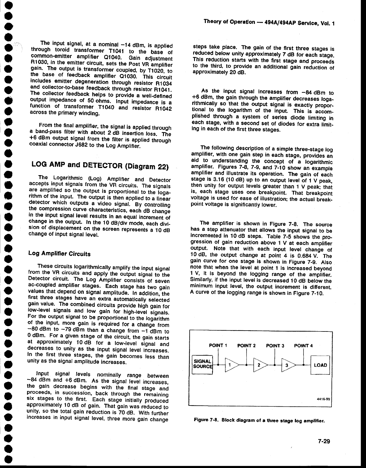
o
a
o
o
o
t
o
o
o
o
o
I
I
o
I
o
I
o
t
o
t
o
o
a
t
a
o
o
I
o
o
a
I
o
)
a
o
o
o
o
o
a
a
a
.. fn9 input
signat.
at a nominal
_14 dBm,
is applied
through toroid transformer T1041 to the Oaii of
common-emitter
amplifier el040. Gain adjustment
Rl0i!0, in the emitter
circuit.
sets
the
posi Vn impfin"i
gain. The
output
is transformer
coupled,
by Tt0i0, to
the base of feedback
amptifier
OiOSO.
ihis circuit
include.s
emitt€r
d€generation
through
resistor
RlOg4
and collector-to-base
feedback
throulh resistor
Rl041.
The collector
feedback
helps
to prorid" a well-deftned
output impedance
of 50
ohms. input impedance
is a
function of transformer
T1040 ana relistor R1042
across
the
primary
winding.
. Fro.m
the
final
amplifier,
the-signal
is apptied
through
a band-pass
filter with about 2 O-e insert
on toss. The
*6 dBm output
signat
from th€ fitter
is afptied
through
coaxial
connector
J6g2
to the
Log
Amplinii.
LOc AMp
and
DETECTOR
(Diagram
22)
The Logarithmic (Log) Amptifier and Detector
accepts
input
signals
from the Vi circuits.
The
signals
are amplified
so the output
is proportional
to the
1-oga-
rithm
of the input.
The
output
ii ttren
applied
to a linear
detector
which
outputs
a video signal. By controlling
the compression
curve_
characteristi-c",
"""h OB
ctranfE
in th€
input
signal
level
r€sutts
in an
equal
increment
of
change
in
the output. In the 10
clBldiv
mode,
each
divi-
sion
of displacement
on the screen
represents
a 10
dB
change
of input
signal
level.
Log Amplifier Circuits
, Tlgr". circuits
togarithmicaily
amptify
the
input
signat
from
the VR
circuits
and apply
the output
signal
to-the
Detector
circuit. The Log'Amplifier
consists
of seven
ac-coupled
amplifier
stages. Each
stage
has
two gain
values
that
depend
on signal
amplitude.-
In
additionlhe
first three stag€s have an extra automatically
sel€cted
gain
value.
The
combined
circuits
provide
high gain
for
lowJevel
signals
and low gain for high-level
-ignals.
For.the,output
signal
to be ploportional
to the log;ithm
of the_input,
more
gain is reguired
for a chang-e
from
-80 dBm to -79 dBm than a change
from _1 dBm to
0 dBm. For
a given
stage
of the cir:cuit,
the
gain
starts
at approximately
l0 dB for a low{evel signal and
decreases
to unity
as the input signal
level
increases.
In
_the
first three
stages,
the gain becomes
tess
than
unity as
th€ signal
amplitude
increases.
^ _lnput signaf levels nominalfy range between
-84 dBm and *6 dBm. As the signat
tev-et
increases.
the gain decrease
begins with the final stage and
proc€eds,
in succession,_back
through
the remaining
six stages
to the first. Each stage
initially produced
approximately
10
dB of gain. That
gain
was
reduced
to
unity, so
the
total
gain
reduction
is Z0
dB. With
further
increases
in input
signaf
level,
three
more
gain
change
Theory
of Operadon
- 4g4A/4g4Ap
Service,
Vol.
1
st€ps take place. The gain of th€ first three stages
is
reduced.
betow
unity
approximately
7 dB for each
itage.
This reduction
starts with the first stage and procee-ds
to the third, to provide
an additionat
gain reduction
of
approximatety
20
dB.
- As the Input signal increases
from _g4 dBm to
19 d?r, the
gain
through
the
amptifier
decreases
toga_
rithmically
so that the output signal is exactly propor-
tional to the logarithm of the input. This ii accom-
plished
through
a system
of seiies diode limiting
in
each stage,
with a second
set of diodes for extra timit-
ing in each
of the first
three stages.
The
following
description
of a simple
three-stage
log
amplifier,
with one gain step in each
stage, proviOls
ai
aid -to understanding
the concept of a logarithmic
ampfifier.
Figures
7-g,
T-9,
and
7-10
show
an example
amplifier
and
illustrat€
its operation.
The gain
of each
stage
is.3.16
(10d8)
up
to an
output
level-of
1V peak,
then
unity
for output
tevets
greater
than
t V peafi tnai
is,.
each stage uses one breakpoint.
That breakpoint
voltage
is used for ease
of illustration;
the actual
break-
point
voltage
is significanfly
lower.
The amplifier
is shown in Figure 7-g. The source
has
a step
att€nuator
that allows
the
input
signal
to be
incremented
in 10
dB steps. Table
7-5 shows
the pro-
gression
of gain
reduction
above
1
V at each ampiifier
output. Note that with each input level change
of
10
dB, the output
change
at point
4 is 0.694
V. The
gain
curv€
for one stage
is shown
in Figure
7-9. Also
note
that
when
the
level
at point
1 is increased
beyond
1.V, it is beyond
the togging
range
of the ampiifier.
Similarly,
if th€ input
level is
decreased
10
dB betow
the
minimum
inpul level,
the output
increment
is different.
A curve
of
the logging
range
is shown
in Figure
7-10.
POINT
1 POINT
2 POINT
3 POINT 4
44 16-99
Flgure 7{. Block diagram of a tfrree stage log ampllfier.
7-29
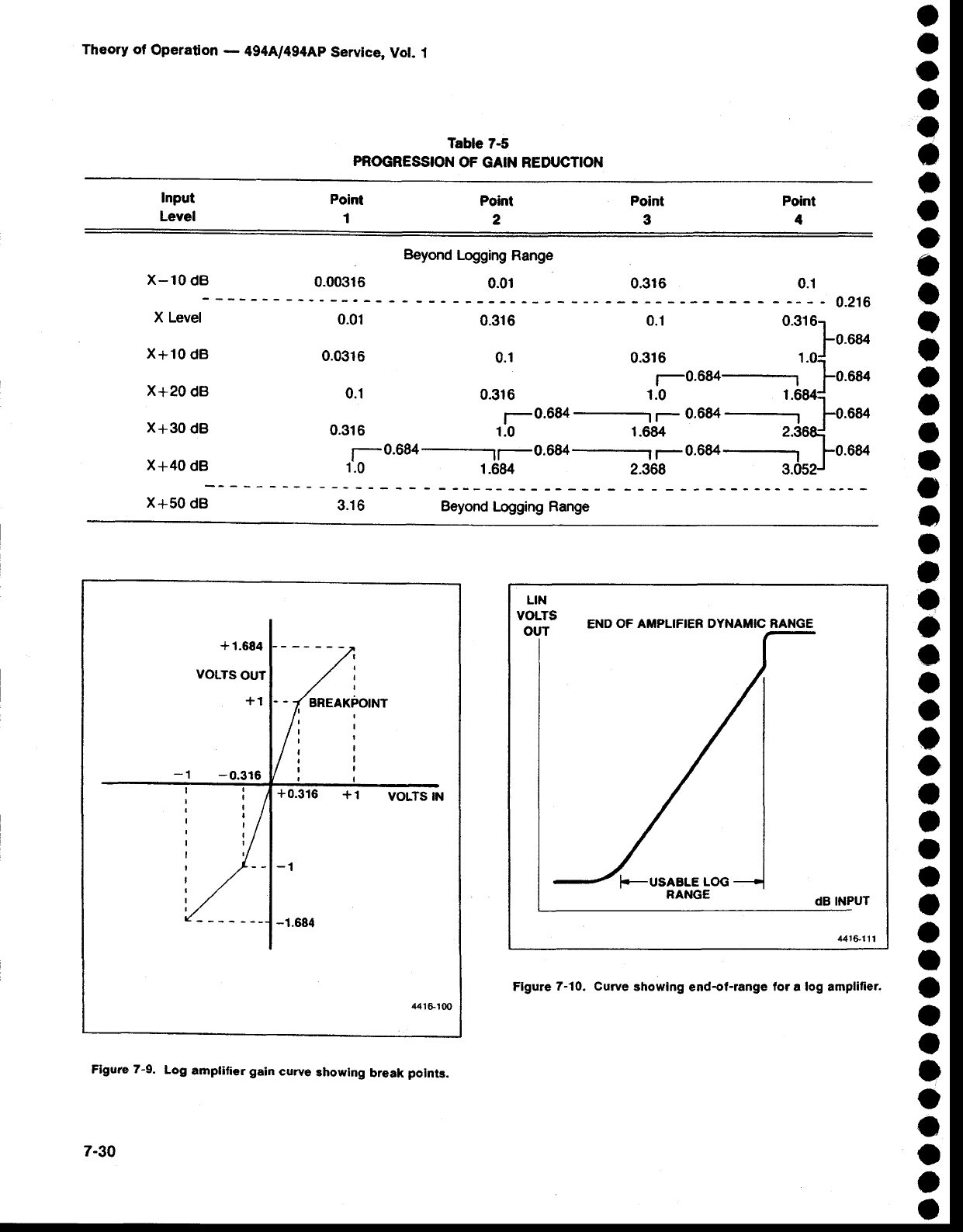
Theory of Operation
- 494A1494Ap
Servlce,
Vot. 1
Table
7-5
PROGRESSION
OF
GAIN REDUCTION
Input
Level Point
1
0.01
0.0316
0.1
0.316
Point
2
0.316
0.1
0.316
Point
3
Poinl
4
Beyond
Logging
Range
x-10 dB 0.00316 0.01 0.316 0.1
- - 0'216
X Level
X+10
dB
X+20
dB
x+30
dB
x+40
dB
0.1
0.316
0.316
1-0.684-1
1.0 1.€
r-0.684 1- 0.684-_-1
1.0 1.684
l_ 0.68a
___r 1_ 0.684
=__1 1_ 0.684
1.0 1.684 2.368
X+50
dB 3.16 Beyond
Logging Range
o
o
o
o
o
,
o
o
o
o
o
t
I
o
o
o
o
o
o
I
t
a
o
o
o
a
o
o
a
,
o
I
t
o
I
o
O
o
I
o
o
o
,
O
Figure 7-10. Curve showing end-ol-range for a log amplifier.
Figure
7-9. Log amplifaer gain curye rhowlng break polnts.
LIN
VOLTS
OUT END
OF AMPLIFIER DYNAMIC RANGE
44r&100
7-30
o
o
o
I
a'
a
o
I
o
a
o
I
o
o
o
a
o
o
t
,
I
o
o
I
a
I
)
o
I
o
a
o
I
o
t
I
O
I
a
o
o
o
o
o
. The 10
MHz
input
signal
from
the
VR
circuits
drives
input
preamptifier
e2075,
in th€ tog lmftiner circuits
on A62A1.
-
The input preamptifier
ir"nsier" the S0O
input signal
to the high_impedance
input of the first
amplifier
stage. The input signal is ilso apptied
to
transistor
01 07S,
a common-base
amplifier
that acts
as
a bufier
to supply
the
l0 MHz
lF signat
to the
rear_panel
connector.
.. Frgm the input preamplitier,
the signat
is apptied
through
seven
cascaded
stages
each
cinsisting'ot an
emitter follower driving a common base amptifier.
Resistors
between
the
emitter
follower
and
the common
base
sections
determine
the gain. Diodes
switch
vari-
ous resitors
in or out of the
circuit
to vary
the
gain
for
different
input levels. All of the "t"g"J are similar,
except
that the first three
stages
"ontaii an extra
set of
diodes for an
additional
gain
itep.
All stages
have maximum
gain for low amplitude
input
signals.
As the
input
amptitude
increases,
the last
stage
switches
to a lower
gain. For
further
increases
in
input
amplitude,
additional
stages
decrease
gain back
to -the first stage. Then the second set of gain-
switching
diodes
switches
into the first, second,
and
third
stag€s
to reduce
the
gain
for
the
larggst
signals.
Typically,
when
the
input
levelto
the emitter
follower
in th€ last stage
is less
than
60
mV peak-to-peak,
the
transistor
conducts
enough
to maintain
fonrvard
bias
on
series
limiting
diodes. The 10
MHz signat
path
at that
level
is through
both
diodes,
a capacitjr,
ani a resistor
network
to the
common
base
section
of
ihe stage.
The
gain
.of the stage under
these conditions
is ipproxi-
mately
10
dB.
- As the input
signal
voltage
increases,
more
current
llows through
the left diod€
to increase
the reverse
bias
of the right
diode. This
sharply
reduces
the
stage
gain
to unity. The
signal
current
then
flows
only
in
the
lower
path
around
the
diodes.
This
change
takes
ptace
during
the positive-going
portion
of each
cycte. tne opposite
occurs
during
the negative_going
pdrtion
of the signal
above the minimum
input level. As the input signal
increases
beyond
the
point
at which
the
gain
of the final
stage
decreases
to unity,
the
same
sequince
occurs
in
the
preceding
stage.
and
in
succession,
back
to the
first
stage.
Theory
of Operailon
- 4g4Ll4g4Ap
Servtce,
Vot. l
Signal
levels
above
this point activate
the second
tier of gain reduction
in the first three stages. These
stages each incorporate a second set of diodes that
r€duces
the gain by another
7 dB. In the first tier of
gain reduction.
reduction started at the last stage and
proceeded
to the first;
in the second
tier,
the reduction
starts
at the first stage
and proceeds
to the
third.
In the first three stages,
the lower
diodes
are for-
ward biased untit the second tier of gain reduction.
With a further increase
in input signai
level,
limiting
occurs
in
the same
manner
as previously
described
and
results in less than unity gain through the stage
(approximatety 112r. The one-two-th6e reducrion
sequence
is established
by the values
of the pull_down
resistors
at
the
cathodes
of the diode
pairs.
Detector Circuit
This circuit
demodulates
the 10 MHz
output
of the
Log Amplifier,
producing
the VIDEO
signal
that drives
the Video
Amplifier
circuits.
The
detectoi
consists
of an
operational
amplifier
with a diode
detector
in the feed_
back path. A low-pass
filter at the output,
shown
on
diagram
23,
filters
the RF
from
the
dEtectlO
signal.
The operational
amplifiEr
is madE
up of common
emitt€r
amplifier
01012 and a differential
amplitier
that
consists
of Q2010
and e20l8. The
summing
node
for
the n€gative
input is the base of e1012 (the positive
input
is
at the
grounded
emitt€r
of el012).
The differential
amptifier's
high impedance
output
allows
it to rapidly
change
during
the
period
when
both
detector
diodes are effectively
open circuited;
that is,
when
the output
is near
0 V. When
neither
diode
is con-
ducting,
it is necessary
that the output
change
rapicfly
through
that
zone.
Figure 7-11 shows a simptified ac-equivalent
schematic
diagram
of the
detector circuit.
Two
detector
diodes are used, but only the negative
half cycle is
taken as the
output. Ac coupling
is used
on both sides
of the detector diodes to prevent ternperature
coefficient
effects of the operational
amplifier from
affecting
the
detector
output.
The detector
output signal
is applied
to the Video
Amplifier. A low-pass filter shown on the foilowing
diagram
compl€tes
the detector
by filtering
the remain-
ing
RF.
7-31
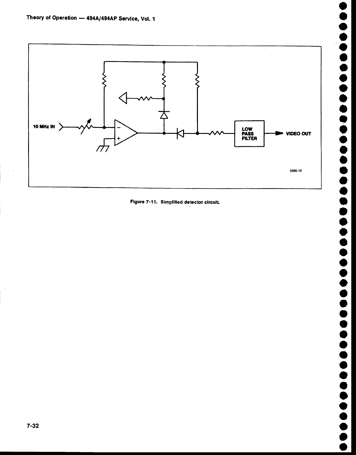
o
I
o
o
o
o
o
o
o
o
I
a
I
o
o
I
I
a
a
a
t
t
o
I
o
o
o
o
o
o
a
o
a
a
o
a
o
t
o
o
a
a
o
o
Theory of Operation
- 4g{A/494Ap
Servtce,
Vol. 1
I
I
o
a
a
t
o
t
o
a
o
I
o
o
o
a
I
t
o
a
I
o
o
I
o
o
I
o
t
o
o
o
I
o
I
o
o
I
o
o
a
o
o
o
Theory
of Operation
- 4g4ful4g4Ap
Servtce,
Vot.
I
DISPLAY
SECTTON
(Diagram
6)
FUNCTIONAL
DESCRT
PTION
The display
section
consists
of the following
major
blocks:
o Video
Amplifier
o Mdeo
Processor
. Digital
Storage
o Deflection
Amplifiers
. Z-Axis
r CRT
Readout
.
The
Video
Amplifier processes
the detected
lF sig_
nal through appropriate
amplifiers
for log and tineir
displays,
and provides pulse stretching for narrow
pulsed
signals.
The Video processor provides band leveling
to
corr€ct
front-end
unflatness
through
the bands,
video
filtering
for noise averaging,
out_;f_band
blanking
to
clamp
the display
to the basetine
when the sweep
is
outside
the range of the selected band, and video
marker
capability
for use
with
a
TV
sideband
adapter.
. Tl" Digitat
Storage
digitizes
th€ video and sweep
signals
and stores
the data
in memory. Stored
data
is
thsn converted
to analog signals for ttre Deflection
Amplifier
and
Z-Axis
circuits.
The
Deflection
Amplifier provides
the drive
voltages
for the cRT. This includes vertical and horizontal
deflection
signals
as well as readout
characters
from
the CRT
Readout
board.
The Z-Axis circuits
receive
and decode
data
from
the microcomputer;
accept control levels ,rom the
front-panel
beam
controls
and generate
unblanking
sig_
nals
to control
the display
appearance,
brightnessl
aid
focus;
detect
power
failure;
monitor
the inJtrument
vol_
tage
supplies;
and
record
the
elapsed
operating
time.
The CRT Readout circuits generate the
alphanumeric
characters
for the
display.
VIDEO
AMpLtFtER
(Diagram
23)
Video signals, from the log amplifier and ctetector
in
the lF section, are received by the Video Amplifier. In
the logarithmic mode, the signals are amplified linearly
and
applied
to the Video
processor. In the linear
mode,
exponential amplification converts the logarithmic aain
characteristic
to lin€ar
function.
In either
mode,
base_
line
compensation
from
the Vid€o
processor
is applied
to the video
signal
to compensate
for any
unflatness
in
the front-end
response.
The
pulse
stretcir
circuit
at the
output
of the Video
Amplifier
atters
narrow pulses
so
data can be acquired
and disptayed
by the Digital
Storage
logic. Signal
amplitude
offset
ciicuits provide
display offset
for the
"ldentify,,mode
operation.
Log Mode Circuits
The log mode circuits
process
the VIDEO
signal
from
the
Log
Amplifier,
and
they add
ofrset
for selecting
that segrnent of the log amplifier gain curve to be
displayed.
The
circuits
also
select
screen
display
gain
steps
from
1
dB/div
to 15
dB/div.
The detected
VIDEO
signat,
the VTDEO
I correction
signal, an offset signal, and reference
current are
summed
at th€ input
to operational
amptifier
U4050.
A
lowpass filter removes l0 MHz from the detected
VIDEO
signal.
The VTDEO
I signat
is adjusted
on the
Video Processor
board (A40) as compensation
for
front-end
unflatness.
The signal
is equal
and opposite
in amplitude
to the unflatness.
Th€ lnput Ref Level
adjustment,
Rl
012, sets the reference
level. Signal
9{"9t is supplied
by digitaf-to-anatog
converter (DAC)
us1
60.
The DAC
converts
the microcomputer
commands
to
an offset signal
that selects
the location
on the log
amplifier
curve tor the disptay
(see Figure
7-12). In
dB/div or log display
modes,
a change
in th6 Vertical
POSITION
control produces
an effect after the log
amplifier
that is the sam€ as a signal level or gain
change
before
the log amplifier. Instead
of using a
large amount
of linear gain before
the log amplifier,
the
output of the DAC effectivety
ofisets ths disptay
up or
down along
the log curve. This offs€t produces
the
same
effect
as varying
the
pOSITION
control
except
the
display
position
does
not change,
only
the signal
level
required
to reach
the reference
level changes.
This
process
allows
the linear
gain
to change while
the top of the screen
is kept
constant,
and
it must also
allow
any 16
dB segment (in
th€ 2 dB/div mode)
to be
displayed.
Nominally,
the log amplifier
operates
with
+6 dBm equivalent
reference
level at the top of the
screen.
The output
ol U4050 is
equivatent
to 20 mV/dB. Futl
screen
is 2.2
V, as set by lnput
Reference
Level
poten-
tiometer R1012.
From
U4050
the
signal
feeds
the log
mode
gain
circuil
and
the lin€ar
mode
gain
circuit. The
digital control
circuit
selects
between
th€
log and linear
mode
circuits.
7-33
Theory of Operaton - 494[l4g4Ap Servlce,
Vol. 1
Figure 7-12. Selecdon ol display positlon on lhe log scale.
Log mode
amplifier
U4030 tinearty
amptifies
the sig-
nal. (fhe log conversion
took place
in the
Log
Amp
cir-
cuit.) At 2.2 V input,
the output
of amptifier
U40S0 is
0 V. This
is the only
voltage
at which
the feedback
cir-
cuit switching
network
resistors
of amplifier
U4030 can
be switched
withont
changing
the output
voltage.
The
switching
network
is
described
later
in this
discussion.
When
the log mode is selected,
the output
signal
from U4030 is applied
through
FET
e5035 to the output
amplifier. Output Reference Level potentiometer
Rl030, in the input
circuit
to U5030,
adjusts
the
output
level for a full screen display after Input Reference
Level
potentiometer
R1012
is set for no change
in the
output of U4030
when
switching
between
the 10
dB/div
and 2 dBldiv modes.
The gain
switching
network
switches resistors
in or
out of the fe€dback
path
of amplifier
U4090.
The net-
work consists
of Q4035,
e4090, e4155, and e4150,
and
associated
resistors.
The FET switches (controlled
by data bits
0, 1,
2, and
3 from
the instrument
data
bus)
switch
in feedback
resistors
lor U4030
in combinations
determined
by
the
four
data
bits.
Linear Mode Circuits
The linear
mode
circuits
accept
the logarithmically
scaled
output
from U4050
and rescale
the signal
level
to linear values. Since
the input
signals
are logarithmi-
cally scaled,
the signal
level
is exponentiated
to operate
the system
in the linear
mod€. High
gain
is required
at
the top of the screen
and low gain
is required
at the
bottom
of the screen
to offset
the characteristics
of the
Log Amplifier
circuits.
7-34
In th€ linear
mode, FET switch
Q5150
is on. ena-
bling the linear mode signal
path; and Q5035
is off,
disabling the log mode path. The output from
preamplifier
U4050
is also applied
to linear mode
opera-
tional
amplifier
U4070,
with a successive
resistor
net-
work switched into the feedback path. From this
amplifier,
the output signal is applied through FET
Q5150 to the summing
node at the input of output
amplifier
U5030.
With a *6 dBm input
to th€
Vid€o Amplifier,
the
out-
put of U4070 is 0 V. This is the level
that represents
the
top ot the screen. At that level,
the foedback
path
is only through resistors R4118
and R5112.
Diode
CR4125
and R41 22 are only activa
when needed
to limit
negative excursions. The other feedback resistors
(switch
transistor emitt€r r€sistors)
ar€ not in the
path,
because the switch transistors
are biased off by the
divider network at the
transistor bases.
As the display
moves
away from full screen,
th€ out-
put voltage of U4070 increases and turns transistor
O4120 on. This places
R4124 in parallel
with
the
tixed
feedback
resistors, thus
reducing
the gain. As the
vol-
tage output increases,
transistors 04125, Q4065. and
04060 start to conduct in sequence,
adding their
emitter resistors across the feedback path. This
effectively reduces the gain of U4070 exponentially.
The transistor
characteristics
smooth
the step transi-
tions, producing a smooth exponential
gain curve.
Diode
CR41
'l
5 provides
ternperature
compensation
for
the switching
transistors.
The Lin Mode Balance con'
trol, R1025, sets the U4070
output
level
to match
the
log mode output.
Pulse Stretch Circuit
The pulse stretch circuit consists of FET switch
Q5026 and the associated components. When the
pulse
stretch mode is not sglect€d
{data bit 7 on the
instrum€nt
data bus is low),
pin 13 of U4020C
pulls
down to -1 5 V, and Q5026 biases off. This removes
C5024
from
the
circuit
and also supplies sufficient nega-
tive bias to keep
CR5025
fonvard biased. With
CR5025
on, the feedback loop for U5030, through
Q5025
and
R5033 is closed so the signal output will fall as fast as
its rise.
when the pulse
stretch
mode is selected
(data
bit
7
high),
the open collector
output of u4020c (pin
13) is
allowed
to float. This turns Q5026
on which completes
the path
for C5024 to ground. During
signal rise
time,
C5024
charges
through the low impedance
of CR5025.
The feedback
path
for U5030
is still closed which
pro-
vides a fast
rise time.
When
the output of U5030
begins to fall, CR5025
turns
off and
the signal
fall
time is now a function
of the
RC
time constant
of R5031 and
C5024.
since the
f€ed-
* *10 dBm
TH|S 16
dB
SEGMENT
LIN
ouT 80 dB Total MAY BE MOVED
TO ANY POSITION
ON LOG
CURVE
dB IN 4416-1
t3
back loop
for U5030
is now
open. Diode
CR5035
turns
on
to prevent
U5090
from
slewing
too
far
negative.
ldentily Circuit
This circuit provides a vertical offset on alternate
lllcg: t9 help
identify
truE and
fatse
signats.
When
the
'ldentify"
feature
is in op€ration,
it allolvs
the operator
to distinguish
between
responses
that result
from sig-
nals
at.
the desired
spectrum
analyzer
input
trequenjy
(true signals)
and those that are produced
by'othe?
spurious
or harmonic
conversions
(false
signats;.
fatse
signals
shift
horizontally
on alternate
trac6s
while
true
signals
remain
in
position.
The horizontal
offset
is accomplished
elsewhere
in
the
instrument
by moving
the 1st
and
2nd
LO
frequency
an equal
and opposite
amount,
related
to the ist LO
harmonic
used,
or by moving
the lst LO twice
the lF
divided
by the harmonic
number
(N),
on every
other
sweep. The result is that any conversion
pioducts
causing
a false
response
will shift a significant
amount
horizontally
on
the
display
while
true
signals
will
remain
close
to each
other.
The identify
offset
circuit
described
here
shifts
the
alternate
or'ldentify"
sweep
vefiically
as a further
aid
to
identify
th€ true signals.
The
microiomputer
sets
DB6
high
during
'ldentify"
sweep
so the
open
collector
out-
put
of U4160A (pin
1)
goes
from
-15V to open.
This
remov€s
the current
normalty
flowing
in R51
54, R51
SS,
and R5158
from the summing
node of U5030 and
causes
a shift
in
the VIDEO
il output
lev€t.
Theory of OperaUon
- 494A1494Ap
Service,
Vot.
I
vtDEo
PROCESSOR
(D|AGRAM
24)
The Video Processor performs four functions.
The
ftrst is compensation
for flatness
variations
in front-end
response.
The second
is vldeo filtering,
which provides
the selection
of six video
bandwidths (90
kHz,
O kHz,
300
Hz, 30 Hz. 3 Hz, and 0.3
Hz) under control
of the
instrument
microcomputer.
The
third function
is out-of-
band
blanking, which
blanks
th€ upp€r and
lower
ends
of the local oscillator
swept frequ€ncy
range
to provide
a selected
window
for the
display. This
function
is also
controlled by the microcomputer.
The fourth is the
capability
to genErate
a negative-going
ditch marker
on
the video display for interfacing
with a 1405
TV Side-
band
Adapter.
Interface with 1405
TV Sideband Adapter
The TEKTRONIX
1405
W Sideband
Adapter
is a
specialized
tracking
generator
that is used with the
Spectrum Analyzer
to analyze
the response
of a televi-
sion transmission
system. The Spectrum Analyzer
monitors
the
RF output
of the
transmitter while
the side-
band adapter
drives
the
video
input
of the
system.
The
video
input
may
be at the
transmitter site,
the
head
end
of th€ studio-transrnitter
link, or the video
switcher
in
the studio. ThE
sideband
adapter
must
be connect€d
to
the lst LO of the Spectrum
Analyzer
by a short
length
of coaxial
cable.
Th€ system in Figure
7-13
depicts a TV
transmitter
operating on Channel 10 with a video carrier at
193.25 MHz. The sideband
adapter
is tuned
to Channet
10. The Spectrum
Analyzer
is tuned to 195.25
MHz
with a span setting
of 1 MHz/Div
(for purposes
of iilus-
tration,
the
sweep
is assumed
to be
halted at
the
center
frequency
of the
analyzer).
The sideband adapter
applies
a2MHz signal
to the
AM modulator
of the
video
transmitter. Th€ modulator
produces
a lower sideband
at 191 .25 MHz, a carrier
at
193.25
MHz, and an upper sideband
at 195.25
MHz.
This signal
is amplified,
filtered,
and combined with
the
FM aural signal. The
composite signal
is sensed
by a
RF pickup
and applied
to th€ RF Input
ot the Spectrum
Analyzer.
The 1st Converter
appli€s
the composite
signal to
the 'l
st mixer. The composite
signal
is mixed with a
2.26725
GHz
signal
from
the
1st LO, forming
three
pro-
ducts. The subsequent
stages of the analyzer accept
onfy
the 2.072
GHz
product
and reject
the
rest. For fre-
quencies
used
in this example,
the
accepted
product
is
the difference between
the 1st LO and
the upper
side-
band
of the
TV
signal.
Digital Control Circuit
The digital
control
circuit
provides
the control
sig_
nals
that select
the various
Video
Amplifier
functioni.
Addresses
78 and 79 are
decoded
by U6160
and sent
through
inverter
U6170
as clock
or enabling
signals
for
gain
latch
u5010
and
mode
tatch
u4010.
Gain latch
lc u5010
is an g-bit
latch
that suppties
command
data to the 8-bit DAC,
USl
60,
to offset
the
Log
Amplifier
output
signat.
Mode
tatch
U4O1O
is an
8_
bit latch
that supplies
command
data
through
the
com-
parators
in U4020 and
U4160
to select
the resistors
in
the dB/div switching
circuit
and
to sel€ct
identify, pulse
stretch,
and log
or linear
mode.
7-35
Theory
of Operaton - 4g4Al4g4Ap
Service,
Vol. I
Figure
7-13. Functonal dlagram
rhowing the Spectrum
Anafyzcr
and 1405
TV Sldcband
Ad.picr System.
The product is converted twic€ more, amplifi€d,
liltered,
log amplified,
and
detected.
This
detectdO
sig-
nal is applied
either
directly
to the video
amplifiers
of
the crt or
to digital storage.
The Spectrum
Anatyzer
lst LO signat
is applied
to
the RF mixer of the sideband adapter. The
2.26525
GHz signal
from the tunable
LO is subtract€d
from the 2.26725
GHz signal trom the Spectrum
Analyzer
LO,
yielding
a ZMHz product.
This
video
fre-
quency
signal
is conditioned
with
sync
and
blanking
sig_
nals and applied to the video input of the T\/
transmitt€r.
When
the
Spectrum
Analyzer
is sweeping,
the video
signal
starts at 3 MHz, lalls to 0 Hz, and rises up to
7 MHz. During
this intervat,
the analyzer
displays
the
lower
sideband
as it moves
toward
the
carrier,
diiplays
the carrier,
and
then
displays
the upper sideband
mov_
ing
away
from
the carrier. Since
the
Spectrum Anatyzer
and 1405
TV Sideband
Adapter
system is similar
io a
tracking
generator
system,
it rejects
nolse and
uncorre-
lated
signal. This allows
normal
in-service
use of the
transmitter
by adding
a tow tevel (1
to 3 tRE
units) cw
signal
to the video
or by using
fuil levets with a ilTS
inserter.
7-36
The sideband adapter can lnsert
frequency markers
at preselected
deviations from the carrier frequency.
Six selectablo
crystal oscillators
have their outputs
mixed with
video
signal and
applied
to a Z-Axis circuit.
This circuit
produces
two n€gative
pulses
as the video
signal sweeps
through tho crystal oscillator
frequency.
These pulses are applied to the spectrum analyzer
mark€r input, whers they appear on the crt as two
notch€s on either side of th€ marker frequency. The
sidEband
adapter allows the width and depth of th€
notches
to be adjusted with the width and
Intensity con-
trols.
Video Marker
The Z-Axis signal
from the 1405
Sideband
Adapter
connects to the MARKER input on the spectrum
analyz€r rear panel. This negative-going signal flows
through the Accessories and Mother boards to the
Video Processor
board. Here, the signal
drives
the
ernitter
of Q4060
and
turns the
transistor
on,
pulling
the
VIDEO
OUT line down. This produc€s
a notch in the
video
signal of the display to signify
the
location of the
marker
on
the display.
RF ln 'l
95.25 MHz/Uppsr Sdeband
t93 25 MHz/Cars
19t.25 MHzIL@d Sirebad
LOAO
trA8X€R/VtO€O
rcll
-2.5 6lt
Oisglay MaA6 h
ffi
rffi
Z-Ax6 o(rl
i\r o.TsMHr
i\o- r.zsMHr
i\\o* sprre
i\o- 3.5s
MHz
i\-..rsMHz
i\'o- 4.75
MHz
!@_f9sEs9Ll9l
Ert. l.Voui
5(n+fi
?.26525
GHz
lst lF + fV Carrs
ToVid@Pcq
a
o
I
o
o
o
o
o
o
t
o
I
a
o
o
o
I
o
a
a
I
o
o
o
o
o
I
o
I
o
o
o
I
a
?
o
O
o
a
o
o
o
I
a
Video Leveling
. -A^mjnor
slope
in frequency
response,
caused
by
the
1.86
GHz
low-pass
filter in the front end, is corr€cted
with band
I Slope adjustment
R1012.
Wiren
operatng
in band
1, contacts
6 and
7 of U3025
are
closed;
therJ
forq a portion
of the PRESELECTOR
DRTVE
signat
is
applied
to the VIDEO
I output signal,
providiig the
ofiset necessary
to correct
slope
difference.
Theory of Operaton - 4g4AJ4g4Ap
Service,
Vol. 1
From
the
normalizer,
the output
is applied
through
a
jumper
switch
to buffer
amptifier
U2OS5B,
which
his a
gain of five, then to offs€t amplifier U2OSsA. This
amplifier
has
a gain
of two, but
its
primary
purpose
is
to
offset
the 0 to +5 V (normal),
0 to -5 V-(invert),
buffer
output
to the levels
required
by th€ Log Amplifier
cir-
cuits.
The range
required
by the Log Amplifier
is O
to
. J-0
V. The output voltage
is a seriss of linear
interpo_
lations
of th€ voltag€
betwe€n
adjacent
trimming
reiis_
tors at the outprrts of the normalizer. Compensation
adjustment
R1065
sets
corect interpolation.
Jumper
ptug
p2060
setects
the input
side
of buffer
amplifi€r
U20558 and proper
ofiset vottage
for U2055A.
This provides
the means
to invert
the buffer output
dur_
ing the instrument
adjustment procedure.
The adjust-
ment procedure
is described
in that section
of this
manual.
As previously
noted, only
band 4 requires
significant
compensaflon.
Selection
of band 4 is indicated
by data
bit
0 switching
to a 1 (see
the Lev€ling
tabte at tire
top
right
_corner
of Diagram
24). When
DBO
is a 1, pins
b
and
2 ot switch U201
5 are connected,
and the output
from offset amplifier
U205SA
is supplied
out as the
VIDEO
I signat.
Minor compensation
is required
for Band 1, to
correct
a minor
slope caused
by the 1.8
GHz
low-pass
filter
and 2 GHz limiter. When
pins
6 and 7 of switch
U3025
are connected,
the
PRESELECTOR
DRTVE
signal
is ofrset
by R4023
and R4011
and Band
Stope
adjust-
ment R1
01
2 to provide an attenuated
negative-going
ramp
to the VIDEO
I output
line.
Switch
Ug02S is con-
trolled by inverter 04025. O402S
is activated
by data
bit 6 going
low. As shown
in the Video
Blanking
table
on
the schematic
diagram,
DB6 is 1 except
when
Band
1
is selected.
Video Leveler
Circuits
. Mdeo leveling
comp€nsates
for analyzer
front-end
microwave
circuit characteristics
that cause unflat
response.
ln
band 4 (5.4
GHz
to 1g
GHz). Since
band 4
is a multiplied
band, any unflatness
is ac"entuatecl.
Leveling
is
accomplished
through
programmable
pertur-
bation
of the
disptay
basetine
[trai
is opposate
in direc_
tion to the flatness
error. As the signai power output
decreases,
the
baseline
rises
an equil amount
to com_
pensate,
and as power output
increases,
the baseline
falls
an
equal
amount.
.The
perturbation
is produced
by
a normalizer
integrated
-circuit
that produces
19 evenly
spaced
valu€s
of the input voltage,
with each valui
corrected
to compensate
for unflatness.
The PRESELECTOR
DRTVE
signat
from the tst LO
driver
circuits
is applied
to a translation
circuit
that con-
sists
of two current
drivers
(U3O45A
and
hatf
of e303g,
plus U30458 and the other half of e303g). The
PRESELECTOR
DRIVE signat is direcfly r€tated in
amplitude
to displayed
analyzer
frequency.
The
nominal
+1
0V to -10V gxcursion voltage versus frequency
9urve1
in maximum
span,
relates
to the
full bandwidth.
This 20
V maximurn
excursion
is scaled
to a precise
current
(from
1 mA at +10
v to o current
at _10
v) that
is applied
to the normalizer
lC to generate
the baieline
perturbation.
Actual
signal
scaling
is done by current
driver
U3045A/Agmg.
The outpui signat
is apptied
to
the normalizer
SWp lN input, pin 5 of U20g9. The
second current driver, Ug04SB/Og03g,
generates a
2 mA reference
current
for the normalizer]
Horizontal
Freq
adiustment
Rl069, in
the input
translation
circuits,
shifts
the 19 evenly
spaced
points
up or down in fre-
quency
to compensate
tor unflatness.
Normalizer
lC U2039
operates
as
a shaper
and
con-
tains 19
transistors
that
turn on and off in sequence
as
the current
input
to pin 5 decreases
from 1 rnA to 0.
Each collector
is connected
to a potentiometer
that
allows
output
trimming. potentiometer
R1061
is active
with
no current,
and
R1013
is acfive
at I mA. The
trim_
ming operation
is described
later.
Video Filter Gircuits
Video filtering provides
selection
of onE of six
bandwidths,
under
microcomputer
control.
As shown in
the
Vid€o Filter
table
on Diagram
24,
data its 1 through
4 select
any of six bandwidths:
30
kHz,
3 kHz,
300 Hz,
30 Hz, 3 Hz, and 0.3H2. Either
wide or nanow-band
filtering
is selected
at the front panel
(Wide
band is
defined
as 1/30th of the selected
resolution
bandwidth
and narrow is defined
as 1/30fth of the resolution
bandwidth).
The microcomputer
makes
the selection,
based on such
factors
as sweep
rate and total
disper-
sion. With no video
filtering
(all data bits are 0), the
video system
bandwidth
is
500
kHz.
7-37
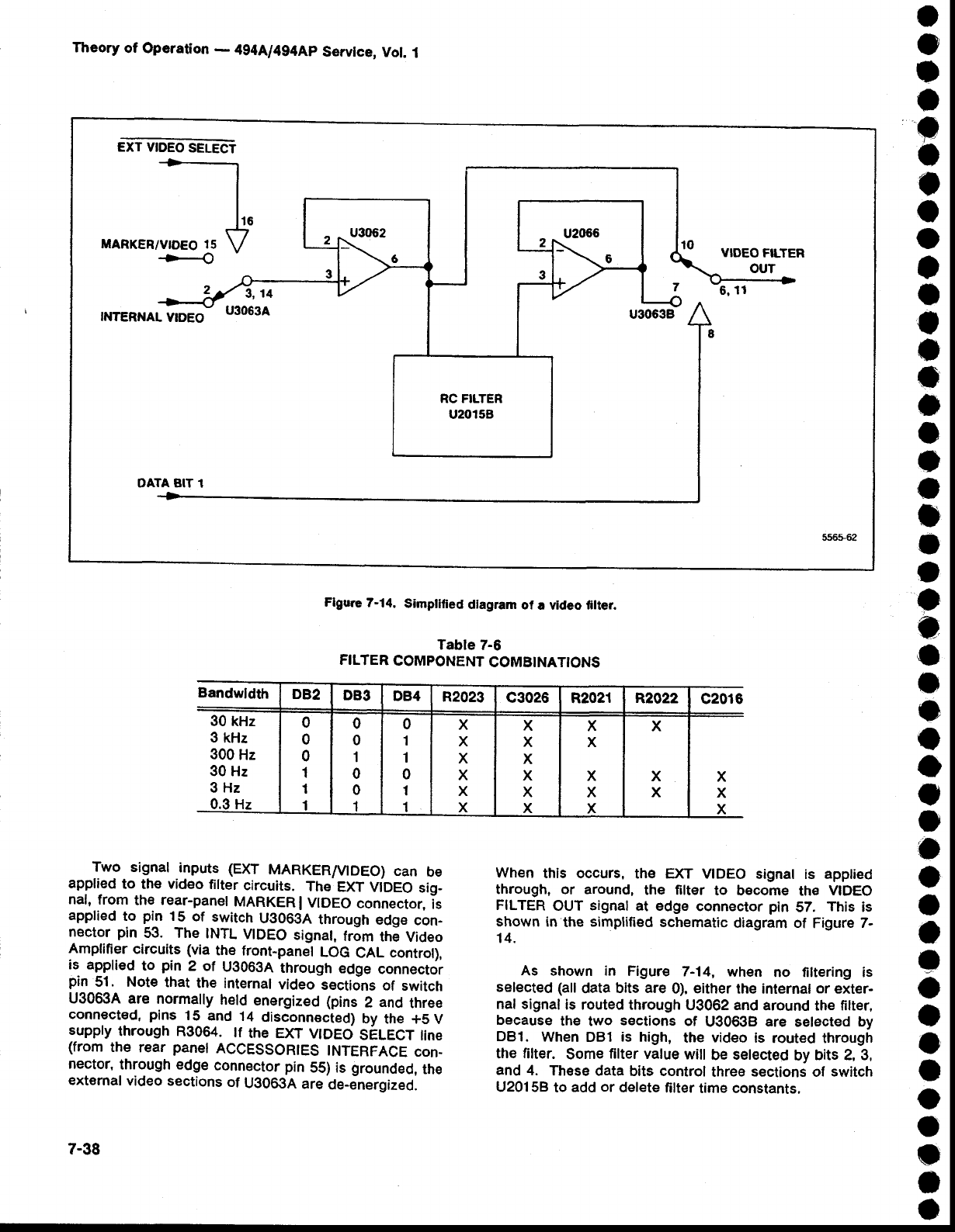
EXT VIDEO
SELECT
MARKER/VIDEO
15 VIDEO
FILTER
OUT
6,
11
INTERNAL
VIDEO
OATA BIT 1
RC FILTER
u20158
Theory
of Operation
- 4g4A/4g4Ap
Servtce,
Vol. 1
o
o
I
a
e
I
f
o
o
t
t
o
o
o
o
o
o
a
o
a
t
o
o
'l
o
o
a
o
o
o
o
o
a
o
I
o
o
J
I
O
o
o
I
t
Flgure 7-14. Simplllied diagram of a video filter.
Tabte
7-6
FILTER
COMPONENT
COMBINATIONS
Two signal inputs (EXT
MARKER/V|DEO)
can be
applied
to the video
filter
circuits.
ThE
EXT
ViOeO
sig-
nal, from
the rear-panel
MARKER
I VIDEO
connector.
is
applied
to pin 15 of switch
U306gA
through
edge
con_
nector
pin 53. The INTL
VTDEO
signal,
from
the
Video
Amplifier
circuits
(via
the
front-panel
LOG
CAL
control),
is applied
to pin 2 of U3063A
through
edge
connector
pin 51. Note
that the internal
video
sectidns
of switch
U30634
are normally
held
energized (pins
2 and
three
connected,
pins
15 and
14
disconnected)
by the +5V
suppry
through
R3064. tf the EXT vtDEo sELECT
tine
(from
the rear panel
ACCESSORIES
TNTERFACE
con-
nector,
through edge
connector
pin
55)
is grounded,
the
external
video sections
of UO063A
are
de-energized.
7-38
Wh€n this occurs, the EXT VIDEO signal is applied
through, or around,
the filter to becorne
th€ VIDEO
FILTER
OUT
signal
at edge connector
pin 57. This is
shown in the simplified
schematic
diagram of Figure
7-
14.
As shown in Figure 7-14, when no tiltering is
selected
(all
data
bits are
0),
either
the internal
or
exter-
nal signal
is routed through
U3062 and
around
the
filter,
because
the two sections
of U30638
are selected by
DBl. When
DB1
is high, the video
is routed through
the filter. Some
filter
value
will be setected
by bits 2, 3,
and
4. These
data bits control
three
sections
of switch
U20158
to add
or delete
filter
time constants.
Bandwldth DB2 DB3 DB4 R2023 c3026 R2021 R2022 c2016
30
kHz
3 kHz
300
Hz
30 Hz
3Hz
0.3 Hz
0
0
0
1
I
1
0
0
1
0
0
1
0
't
1
0
1
1
X
X
X
X
X
X
X
x
X
X
X
X
X
X
x
x
X
X
X
xX
X
The
filter
consists
of resistors R2O2g,
RZOZ1,
R2022
and capacitors
C3026
and C2016,
"onn""t"O between
U3062
and
U2066.
Tabte
7-6
lists
itre
tiiiei components
in thE
circuit
for each
of the
six
OanOwiOttrs.
Data
bits
2,
1: "1! 4 are
apptied
to switch
U2O15B
(pi-ns
B, 16,
and
9) which selects
the components.
frorir U2OOOB,
the
signal is routed through contacts Z ana
6 of switch
!9.qpp to. edge
connector
pin
57
as
th€
VtoEO
FILTER
OUT
signal.
Video Blanking
The
video
btanking
circuits
allow
selective
blanking
9l_!h" lower and upper ends of the locat osciilator
range. Selective
blanking
is required
because
the
local
oscillatgr
sw€eps
the fuli span-regardless
ot the
band
IT,r-.:,].P.,:9:?
s_y:tem
is
desisn;c
to
"tr""tiu"ry
op"n
a.otsptay
window
only
during
the
time
for display.
Data
bits 5, 6, and 7, under coritrol of the
-*iiro"orput"r,
select
the appropriate
amosnt
of display
for
eacn
end.
.
Video
blanking
and
the PRESELECTOR
DRTVE
sig_
nal (which
provides
frequency
information,
in voltag-e
rorm) are located on the ViOeo processor board.
::1,:h_ yg.0g3.
incorporates a disabte function rhat,
wnen provicted
a tow input,
opens
all switch
s€ctions
regardless
of individual
section input. This feature
allows the VTDEO
FTLTER
OUT signat
to be easity
blanked
at wiil.
The disable
function
is controlled
by a combination
of outputs from comparators
U30154 anO UgolsB.
I11ttlq.these comparators
are
from the PRESELEC_
TOR.
DRIVE
signal
and a combination
of vottage
divid-
ers
that
are
switch
selected
under
control
of dai=a
bits
5,
5, and 7. The
PRESELECT_OR
DRTVE
signat
is applied
from edge connector
pin 54 through
OiiiJer
resistors
R4013
and
R4012
to the
inverting
iriput
oi UgOtSR,
anO
through
divider
resistors
R4014
inO'Ra0tito the
non_
inverting
input
of U3O15B.
These
dividers
rectuce
the
excursion
of the drivE.signal
from
(+10V
to _10V)
to
(2.5
V to -2.S
V),
which
is the maxlmum
input
tevet
to
the comparators.
Input
to the non-inverting
input
of U3015A
is from
divider
resistors
R9011,
RgOl
d and selected
r€sistor
R4015.
The
inctusion
of R4015
is controlted
by DB7
through pins
2 and
3 of U9025.
The
junction
of divider
resistors
R3011
and Rg0l2 is connected
to ground
through
R401S
for
band
2.
Input
to the
inverting
input
of Ug01
58 is from
divider
resistors
R4018,
R4012,
and selected
resistor
RgO2g.
The inclusion
of 83023 is controlleO
Oy
OeO
through
pins
10 and
tl of U3025.
The
junction
oi Rg0t anO
R3012
is connected
to +S
V ttrr6ugn
RO0rS
when
it is
selected.
This switching
arrangement
of negative
and
positive levels for comparisbn with the reduced
PRESELECTOR
DRIVE
signat
enabtes
the iop and
bot_
Theory
of Operation
- 494Al4g4Ap
Service,
Vot.
i
tom
extr€mes
of the frequency
excursion
to be
blanked.
The blanking
is activated
by the disable
function
of
switch U3063,
which is controlled
by the microcom-
puter.
DlclTAL
STORAGE
(Diagrams
25 and
26)
The Digitat
Storage
circuits provide
the abitity
to
store and process
a signal
before
displaying
it. fnis
allows flicker-free
displays,
Even
at tire'stow swesp
rates required for narrow resolution bandwidth
meaj-
urements.
Digitizing
the signal
also allows
signal pro-
cessing
and
marker generation.
.- - Th-"
processing
includes
detecting
peak
amplitudes
(Max.Hold),
storing
a signat (Save
A),'subtracting
one
signal from another (B-Save A), signal averiging
(Averaging),
and signal
comparison
(View
A anO
Vei
g)t These operations use two memory banks to
independently
store
two complete
signals
tirat
are
Each
digitized
at 500 points
across the
lweep. Therefore,
two signals
may be observed
simultaneousty
or pro-
cessed
in separate
ways.
The markers are used in a variety of ways. There
ar€ two waveform markers
that th€ user sets for vari-
ous measurements.
In addition, an update mad<er
shows
where
the actual
sweep
is with reierence
to the
refreshed
display.l
Four
instrument
bus
addresses
are associatgd
with
Digital Storage. Addresses 7A and lB are write
addresses.
FA and
FB
are read. These
addresses
are
shared by both the Horizontal
and Vertical Digital
Storage circuits. Logic on the Horizontal Oilitat
Storage
board controls
which set is activo. 7A onlne
Horizontal
Digital
Storaga
board is further
subdivideO
into I subaddresses
by 3 bits in address
ZB on that
board. Address
tables
in the
circuit
descriptions
for
the
appropriate
boards
show
details
of the Digital
Storage
addresses
In the Max Hold mode, the highest
amplitude
at
each
of the 1000
points
in successive
sweeps
is
stored
and
displayed.
ln the
Save A mod€,
a signal
is stored
in
one memory
for later
examination,
and is not updated.
In the B-Save A mode,
the A signal
is stored
and
not
updated,
then arithmeticaily
subtracted
from
the B sig_
nal, which is stored, but continually
updated. tn ttre
averaging
mode,
the display
area
is divided
by a hor_
izontal cursor. Signals above the cursor are peak
cletect€d
and displayed,
and signals
below the curcor
are averaged.
ln the View
A and View B modes,
the
contents
of the selected
memory or memories
are
displayed.
_89t9_are als"-rid* rnarkers lhat may be fed to the ,ear-panel
MA8KER I VIDEO input These video mdrkers are from an exliernal
source, and are not part of the digital storage system. See the
vroeo processor description for more informaiion about the video
matkers.
7-39
Theory
of Operation
- 4g4A/4g4Ap
Service,
Vol. 1
Graphical
presentation
of mathematic
functions
or
experimental
data is common.
one such graph
has a
single
Y value
for each
X value.
An alternaie
presenta_
tion of the data in this graph
would
be a table
simply
listing the
x coordinate
values
along
with a correspond-
ing Y value
for each X value.
To further simpliiy
the
graph, if the first X value and the spacing beiween X
values
were known (all spaces
assumed
equal),
the
two-column
table could
be reduced
to a single
column
with
the X value
implied
by
the
position
of the
y value
in
the
column.
This
is the essence
of cligital storage
_ to
convert a vertical
analog
voltagg
(y coordinate
value)
to
a biiary number
and insert
that number
in a stored
table. Th€ location
of the y value
in the table
is deter-
mined
by the
analog
sweep
voltage (X
coordlnate
value)
binary conversion.
Once a s6t of binary numbers
thai
rspresent
values
across a waveform
is stored
to cr€ate
a table, the waveform
can be recreated
at any time by
conversion
of the
table
vatues
(y)
and
positions
(X)
baci<
to analog voltages
that represent
amplitude
and
sweep
positions.
The digital storage
system
uses a Tabte
A and a
Table
B. Table
B is updated
every
sweep.
Tabte
A is
also changed
unless the Save A mode is selected.
There are
500 A values
and
500 B values.
The
spacing
between values
is the same
throughout
both
tables,
but
the starting
point
for Tabte
B is shifted
stighfly
so that
when
both tables
are
read,
thE readout
values
are
inter-
laced.
When
the signals are recreated,
the contents
of
either Table
A or Table B can be displayed,
or both
tables A and
B can
be
displayed.
tf both
Tables
A and
B
are
to be displayed,
and
thg Save
A mode is selected.
the contents
of both Table A and Table B are drawn,
each
display in its own trace. lf the Save A mode
is not
selected,
the contents
of both Table
A and Table
B are
displayed on one trace, with 1000 value positions
across
the screen.
A third
trace option
is also
available.
In the
B-Save A mode,
the
displayed
values
are
those
that r€sult
from an arithm€tic
op€ration
and are the
difference
between
the contents
of
Table
A and
Table
B
for each
X value
of anatog
sweep
voltage.
Since
a signal
waveform
is continuous
and
a table
has discr€t€ X values,
an algorithm
determines
the y
value
to be stored
for a particular
X valus.
This
allows
the operator
to select
one
of two methods
to determine
Y values;
peak
or average.
The
y analog
voltage
is con-
tinuously
sampled,
with the sampling
rate dep€ndent
upon
sweep
speed.
For each
X value,
there are
always
at least two samples,
and
there
may
be as many as
217
samples. From
this set of samples,
either
the largest
sample
value (peak
value)
or the mean
of all the sam_
ples
(average
value)
can
be s€l€cted.
Selection
between
pgak ancl averag€ ls controlled by the front-panel
PEAK/AVERAGE
control,
which
sets a dc level
that is
eompared
with
the analog
vertical
input
to produce
the
PEAK/AVG
logic
signat.
When
the input
signat
is below
7-40
the level
selected
by the front-panel
control,
the signal
is averaged; when
the input
is above
that level,
the
peak
signal
is displayed.
The
dc level
appears
on
the
display
as a positionable
horizontal
line. This line is created
when
the dc level is switched
to the analog
output line
during the cursor cycle
by the CURSOR logic
control
signal.
Superimposed on the cursor line is an intensified
spot called
the update
marker,
which indicates
the X
value at which new Y values
are being computed
for
display
update. The update mark€r
is formed
when
the
analog
sw€ep input
is compared
to the display analog
X
output.
When the
two are
the same value,
the sweep
is
forced
to pause,
which
increases
the
marker
intensity at
that
point.
Two custom
integrated
circuits
are th€ heart
of the
digital storage circuits.
Th€ v€rtical
control
lC contains
the vertical
acquisition
and display logic,
peak
detec-
tion, signal
averaging, Z-Axis
blanking, and special Y-
value
processing
circuits.
The horizontal
control
lC con-
tains the horizontal acquisition
address counter,
hor,
izontal
display counter, 10-bit
RAM address
multiplexer,
and a system control matrix. Th6 other digital storage
control circuits consist of two 8-bit digital-to-analog
converters,
two 1O-bit
digital-to'analog conv€rters,
one
10-bit latch, 8K bits of random
access memory,
and
various auxiliary circuits.
Timing is controlled
by OZ
ctock pulses
(at 1 MHz) from the Processor
board to
the Horizontal Digital
Storage
board.
Vertical Section (Diagram 25)
The Vertical Control lG block diagram
is shown in
Figure
7-15. The
vertical
analog voltage
is converted
to
a Y binary value by an 8-bit successive
approximation
register. Nine clock cycles are required
for each Y
conversion.
After the conversion
has taken
place,
the
successive approximation register produces the
negative-going
SYNC
signal. Most functions
on both
th€ vertical and
horizontal
control
lCs arE synchronized
by this signal. On the negative-going
transition
of
SYNC, the successive
approximation
register is reset to
10 00 00 00 (binary)
and the next conversion
cycle
begins. Incoming data
bits ar€ latched into
the
register
on th€ negative-going clock
transition.
From
the
regis-
ter, the output data is applied
to the peak and the
averaging
circuits.
The averaging
circuit
consists
of three
groups
of
cir-
cuits;
those that
accumulate
all
the
Y values for a given
X value into
a grand
total (called
the
numerator),
thos€
that count the number of samples
that make
up the
numerator (this total is called the denominator),
and
those
that subtract
and shift
to divide.
o
o
I
o
a
o
t
o
o
o
o
o
I
I
o
t
o
t
e
I
a
o
I
a
o
o
o
o
t
o
o
o
o
o
I
o
I
C
I
o
t
T
o
I
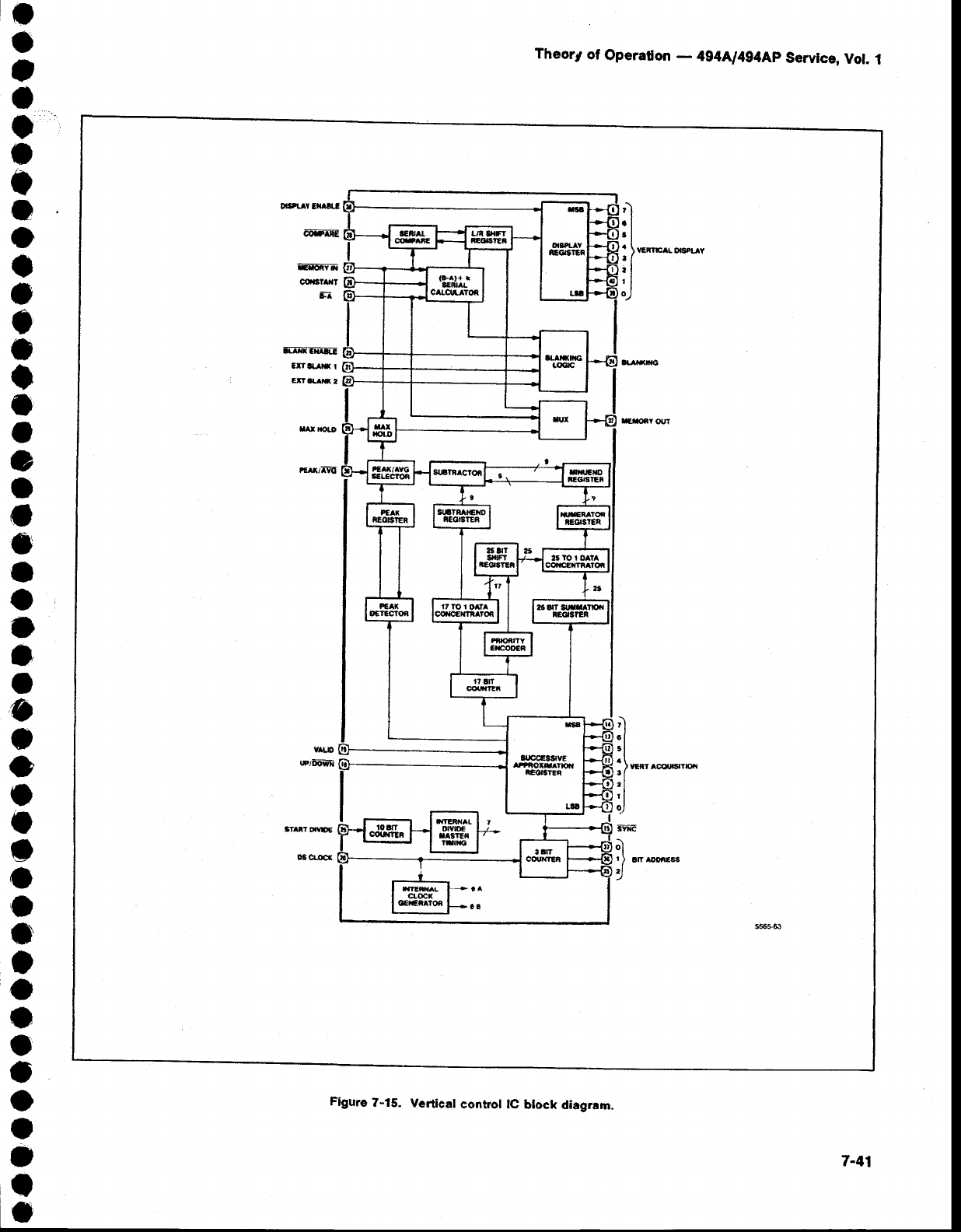
n
I
.l
"l
I )"t*^.ocr-t
rl
'l
o)
__l_,
I rEmal t+t^
I cfocr( I
IqECR^ron
FoD
Theory
of Operadon
- 4g4N4g4Ap
Servtce,
Vot.l
o
a
.
o
I
o
I
o
o
o
o
o
t
t
o
I
a
t
o
c
a
o
)
)
O
e
o
o
o
I
o
o
o
o
t
o
o
o
a
o
o
t
I
o
Figure ?-15. V.rtical confol lC block diagram,
Theory of Operation
- 4g4Ll4g4Ap
Servlce,
Vot.
1
As each
new Y value
is converted.
it is added
to the
eight
least significant
bits of th€ numerator.
Each
carry
from the most significant
bit of this addition
is counted
by a 17-bit
ripple
counter.
The contents
of this counter
and the 8-bit
sum are
cascaded
to form a 25-bit grand
total.
Each
time a new
sample
is added
to the numera-
tor, another
17-bit
ripple
counter
is incremented
to pro-
duce the denominator.
A division cycle
starts
when
the horizontal
control
lC
(on the Horizontal
Digital storage board) detects a
change in ths x value.
At that tim€ it generates
th€ sT
DIV
(start
divide) signal.
On
receiving
this
signal,
and
in
synchronization
with the SYNC signal,
verticat
control
lC U2030
does five
things
(refer
to Figure
7-15):
1. Latch€s
the current
numerator
in a 25-bit
latch
(25-to-1
data concentrator)
and latches
the denomi-
nator in a 17-bit
latch (17-to-1
data concentrator).
2. Clears
the numerator
adder
circuits
(25-bit
sum-
mation
register).
3. Performs
a 17-bit
priority
encode
on the denomi-
nator and loads
a 1 in the appropriate
cell of the
25-bit
shift
register.
4. Loads the latched
nurnerator
and d€nominator
serially
into the divide
circuit (subtractor)
using
the
contents
of the
25-bit
shift
register
as a mask.
5. Clears the denominator
ripple counter
(1
Z-bit
counter)
to zero.
Ten clock
periods
are required
to load
the numera-
tor and denominator
into the divide
circuit.
The cycle
starts
on a SYNC
pulse.
The lirst bit of the quotient
is
available shortly
aft€r
the first clock
pulse
that follows
the
next
SYNC
pulse.
Division
is performed
by
repeated
subtract and shift
operations.
Th€
quotient
is arrived
at
serially with
the most
significant
bit first.
Since onty
g-bit
accuracy is required,
with the priority
encoder
output
used
as a mask,
the
divider circuit
is loaded
with
the g
most significant
bits of the denominator
and the 16
most significant
bits of the numerator. (Ripple
borrow
for a 17-bit
by 25-bit
subtractor
woutd
be so tong
that
it
would be
impractical.)
The peak
circuit
consists
of a peak
detector and
an
8-bit
peak
shift
register.
In operation,
the
previous
peak
Y value from
the last
set
of samples
is still
stored
in
the
peak
shift register
at the start
of a conversion
cycle.
At
that time, the peak
detector,
which is a serial
compare
circuit,
is set
to the state
that
qu€stions
whether
the
old
or new number is larger.
Each
bit of the new
value
is
then compared
with the corresponding
bit of the old
value,
most significant
bit first.
When
one
value is
found
to be larger,
a flipJlop
is set and
the smaller
number
is
gated
out
of the
shilt
register.
The start
divide logic sig-
nal being
true then forces
the peak
detector
to select
7-42
the new value and ignore
the
number
in the
shift
regis-
ter.
The peak/average
selector. a multiplexer, selects
either the peak or average value to b€ routed to the
memories under conrol ot the PK/AVG signal. The
selector
output
is routed
through the Max Hold circuit.
which
functions
like
the p€ak
detector.
When
the MAX
HOLD signal
is high,
the value
that is routed
to the out-
put multiplexer is the larger of two values:
the current
memory value at the subject X coordinate or the
previously-selected
peak
or average
value.
Timing
to set up the divide operation
and clear
the
numerator,
denominator,
and peak
circuit
is controlled
by a 1O-stage
countEr. Taps are
taken
from appropriate
sfages
to develop the necessary clear
and
latch
timing
puls€s.
All data
enters
and
leaves
th€
mgmory
serially. Data
read from memory
enters an 8-bit shift register
and,
timed by the SYNC
signal,
is transferred
to the
vertical
display output
latch (display
register). The same
shift
register
is used for other purposes,
so the DSPL
EN
(display
enable) signal
prevents
non-display information
from being
transferred to the
output
latches.
An
exam-
ple
of data
moving
through this shift register
is sEen
in
the B-Save A display mode. The A value is first read
lrom memory and stored in the shift register. As the B
value
is read, the subtraction is done
serially
and
the
answ€r
is applied to the shift register.
Since the sub-
traction must
be perforrned
with
the
least signiticant
bit
first, a set of exclusive-OR
gates
change
the order of
extracting B lrom memory.
The shift register
direction
is
reversed
to present th€ most signiftcant
bit to the
proper
display
latch. The shift register output is also
applied
to the
output multiplexer.
In subtraction,
the operation
performed
by
the
serial
calculator
is not merely B minus A. The actual expres-
sion implemented is (B-A) + K, where K is a serial
input external
constant
specified
by the user.
This
per-
mits zero to be placed anywhere
on the screen. To
avoid confusion
when
(B-A) + K results in an off-screen
position,
the subtractor blanks the display.
(Ihe sub-
tractor
examines the carry
bit and
borrow
bit when
the
most
significant
bit is calculated. lf either bit is a 1, the
screen is blanked.)
When
the Save
A mode is not selected
and
both
A
and B are being displayed,
maximum resolution
is
obtained
(1000
points
across
the display).
lf this display
includEs a very
narrow
pulse,
it is possible
that
the top
of the
pulse
is only
as wide as a single X coordinate.
lf
this maximum
value
were in
the
B Table and
the
Save
A
rnode was selected
and B turned
off,
there
would be
an
apparent
drop
in amplitude. So,
when
the Save
A mode
is selected, a special
set of circuits in U2030
compares
all A and B values that have
the same X value,
and
stores
the larger
in Table A. The B value is read
and
t
o
)
o
t
t
I
o
o
o
o
o
I
I
a
o
o
I
o
I
o
o
o
a
o
o
I
o
I
t
o
o
o
o
o
o
I
D
o
o
o
a
t
o
stored
in the
display
shift
register.
Then,
as
th€
A value
is- read.
it is cornpared
with
the B value
and
the larger
of the two is loaded into the disptay
shift regisier.
Finally,
the number
in the shift registei
is writte; into
memory._
This operation
is performed
once each
time
that
th€
save
A mode
is selected.
Vertical
control lC U2090
contains
a 3-bit synchro_
nous
counter
that id€ntifies
the specific
bit of in g,bit
vertical
value
that is to be read from memory
or written
into
memory.
This
is
the
only
memory
addressing
that
is
performed
by U2030.
All other
addrdssing
is performed
!y tne horizontat
control
lC (on the Hoiizontat
Digital
Storage
board).
Dlgltzlng Clrcults. The input vertical
signat,
VtD
FLTR
OUT, coupled
through
edge
connector pin 60 is
applied
through
buffer
U3040
to sampte
and hoid
switch
U2040C.
U2040C
is controiled
by frip-flop
U10108.
U10108
generates
the sample puise,
and is enabled
9uljng
the ctock
cycte
after tne
iast approximation,
as
indicated
by
the
least
significant
bit trom
the
successive
approximation
register
in U2030.
The switched
sample
is then applied
through
buffer
U1045
to a summing
junc_
tion. At this point the output current
from Oigitifto-
analog
converter
Ug02S,
that is supplied
from the suc_
cessive
approximation
register
in Ui03O,
is subtracted
from
the sample
current.
The
difference
current
is then
fpRlieO
thr-o-ugh comparator
U2O3SB
and synchronizing
flip-flop,
y:2027A,
to pin 18 of U2030
as th; UpiDowti
slOnal.
The binary
equivatent
of the input sample
is
sfiectively
produced
by the combination
of the succes-
sive approximation
register,
the digital_to-analog
con_
verter,
and
the
sample
and
hold
circuit.
Address Decoding. The address decode logic
accepts inputs from the address bus and trom the
address
control
logic on the Horizontal
Digital
Storage
board,
producing
the control
signals
for read
and
wri-te
operations:
CONT W
(control
write)
DATA
W (data
write)
DATA R (data
read)
The
control
write
signal gates
the
control
word
from
the data bus into control register
UZOZ'
to generate
mode
control
signals.
This
control
word
consists
of one
bit, 04, that
represents
the front-panel
MAX
HOLD
func-
tion.
lf output
Q5 is low, a peak
operation
is forced;
if
output
Q5 is high
and e6 is low, an average
operation
is forced.
The data read and data write signals
are
applied
to the interface
logic to control
memory
read
and
write
operations.
Theory of Operatlon
- 494A/4g4Ap
Servlce,
Vol. I
Interface
Logic.
The interface
logic,
in general,
per-
forms
control and interface
functions
between
the active
data
circuits in the vertical
and
horizontal
sections
and
the rest of the instrument.
lt allows
the microcomputer
to control
the storage
system
functions
and to access
the
digital
storage
memory.
lt also
contains
th€
circuitry
for serial-to-parallel
and parallel-to-serial
conv€rsion.
(l'he microcomputer
uses parallel
transfer;
the digital
:lollSe memory uses seriat transfer.) Shift regaster
U4020
reads
data from memory
to the data bus. Regis-
ter U2025 stores information from the data bus for
transfer to memory. Multiplexer
U40i
5 does the
parallel-to-serial
conversion
and
applies
the
data
output
to gate
U30248, which
acts
as a buffer
to supply
eitirer
the multiplexer
output
or the MEM
OUT
(memory
out_
put)
signal
from
U2030
to the memory
as
the DSDa
(digi-
tal storagE
data Input)
data
train.
The interface
circuit group on the Vertical
Digital
Storage board is the handshake
togic that works with
the horizontal
control
circuits
to access
th€
mernory and
to determine
when to increment
the memory
address
counter.
In either
a data read
or data write operation
(when th€ corresponding
signal goes high), flip-flop
U30208
is triggered. This reteases
the BUS REe (bus
request)
line
to allow
that signal
to go high
and signats
the horizontal
control circuit that memory
access
is
required.
When th€ horizontal
circuits recognize
the
request.
thos€
circuits
pull
the BUS
REO
line low
at the
same
time
that SYNC is low.
The interface
logic
detects
the BUS
REQ
and
SYNC low
condition
through
U201SA,
U20158,
U3010A, and U3015A,
and produces
the tow
BUS GRANT signal
to indicate
memory
access.
The
BUS
GRANT signal
then enables
shift
register
U4020
to
shift
data from
memory
or enable
register
Ul02l . BUS
GRANT also enables
multipl€xer
U401S
to Ehlft
data
to
memory
as indicated
by the DATA
R and
DATA W tines.
At the end of a data read cycle, gates U2010B and
U4030C
produce
the INCR
ADRS (increment
address)
signal
to increment
the
address
register
in the horizon-
tal circuits.
Maximum Hold.
As described
previously,
when
the
Max
Hold
mode
is selected,
the signal
from
e4 of con-
trof
register
V2428
causes
th€ circuits
in Ul023 to com-
pare
the binary
equivalent
of th€ input
signal for
a giv€n
X value
with
the
information
in memory
for that
same
X
value.
This causes
the larger
value
of the two to be
stored
in memory. The signal
from
04, in combination
with
the VALID signal from
the horizontal
circuits,
pro-
duces the MAX HOLD command
to U2090 through
inverter
U4030E
and
gate
U4040A.
Constant Circuit As described previously,
in the B
minus A operation,
a constant
is
used. This
constant is
selected
internally with
switch
3101
5, This switch,
in
7-43
Theory of Operation
- 494A1494Ap
Service,
Vot.
1
combination
with multiptexer
U2020,
suppties
the
CON-
STANT data to U2030. Muttiptexer
U2A2O
is, in turn,
controlled
by address
bits 0, 1, and 2 to provide
the
proper
constant
data
bit to u2030.
Output Clrcults. From the U2030
verticat
display
register,
the parallel
data output is applied
to 6-Oit
digital-to-analog
converter
U1035.
The
convefter
output
is then applied
to the output storage/cursor
switch,
U20408,
through
a vector
generator
that
consists
of an
integrator
(Ul040 and
Cl03S) with an associated
feed-
back loop sample-and-hotd
circuit.
Integrator
Ul040 has
a time constant that provides
a ramp to tast between
the existing sampl€ and the new sample (that is,
between sync
pulses).
Circuits U2M0A and U2045 and capacitor
C204S
make
up
a sample-and-hold
circuit
with
U2045 acting
as
an output buffer. From U2045, the output current
through resistor R1036 subtracts from the digitat-to-
analog converter
output current
to modify the slop€ of
the output ramp.
The output of the vector g€nerator
is
then applied
to switch
U20408.
U20408,
controlted
by
the MKR (marker)
signal
from the horizontal
section,
selects
between
the recreated
video signal
from
u1040
and a dc (Peak/Average)
level from buffer U304S,
to be
sent out as the v€rtical
signat.
The
dc level
is displayed
only during rotrace
as the PEAK/AVEBAGE
cursor.
Peak/Average Level Circults. The buffered
PEAK/AVG LEVEL
signal,
from U3045,
is compared
with the sampled
Video
Fitter
Out signat,
from U1045,
by comparator
u2035A.
The output of u2035A
is a high
(1) if the video Fitter
out signal is greater
than the
PEAK/AVG
LEVEL,
or tow if it is tess.
This output
com-
mands
U2030, via U4040C and U4040D,
to send
peak
or average
data
to the output.
U40408,
C, and D are
used if the instrument
is under
GPIB control
to select
one of three possible
modes;
peak,
Average,
or front
panel
control knob.
Horizontal
Section (Diagram
26)
Figure 7-16 is a block diagram
for the Horizontal
Control lC U5020. The
horizontal
analog
vottage
is con-
verted
to a current
table value
through
a 1O-bit
tracking
analog-to-digital converter (adc), which consists of
up/down interlock and 1O-bit up/down counter in
U5020, and external
10-bit
digital-to-analog
converter
(clac)
U4040.
As the sweep
movss right, the counter
Increments;
as the sweep retraces. the counter decrements.
Each
time the
counter
increments,
it generates
a new
X coor-
dinate value
(the dac input) and a ST DIV (start ctivide)
signal to start the storage cycle. The increment
clock is
the SYNC
signal,
and
th€ decrement
clock is the basic
digital
storage clock divided
by two. When
the Save
A
mode
is selected,
the counter
skips every
other
binary
nUmber, so only
B coordinates
appsar
as addresses.
A state machine provides the horizontal syst€m
intelligence.
This
circuit
determines
which
trace to write
on the screen,
determines
when
to switch from read to
write, generates
the B-A coordination signals for verti-
cal control lC (on th€ Vsrtical Digital Storage board),
controls the g-bit display counter incrementing,
and
proc€sses
requests for the memory bus.
When an
external
device
€lects
to read from or write
to m€mory,
it allows
the BUs REQ
(bus
r€quest) signal
to go high to request permission
from the state
machine.
When
the time becomes
available,
the state
machine
pulls
the BUS REQ line low, which signals
the
start of a request
cycle,
For
the next eight clock
cycles,
the internal multlpl€xer
output lines are in th6 high-
impedance
(open)
tri-stats
modE.
The combination of the up/down interlock, 10-bit
up/down
regist€r,
9-bit display
counter,
and horizontal
display multipl€xer
constitute thg primary
circuits
that
either write to or read from m€mory. To generate
X
values to be written into memory, the circuits convert
the sweep voltage
to binary
form. These circuits also
count the sync cycles to cause the external logic to
read stored data from m€mory and produce a vertical
signal
(Y
value)
for each
corresponding
X value.
During acquisition cycles, the 10-bit up/down
counter, controlled
by the up/down
interloclq
operates
in a loop
with the external
10-bit
digital-to-analog
con-
verter. This allows
the counter to acquire
the
equivalent
(X value) of a sample
section
of the sw€ep
voltag€.
From
the
counter,
the 10-bit
output is applied to the 10-
bit up/down
register. During
display cycles. the g-bit
display counter counts sync pulses
to acquire the x
value. Either the 1o-bit
up/down
register output
or the
display
register
output is applied
to the
horizontal
multi-
plexer under control of the SELECT
signal from the
State Machine. From the multiplex€r,
th€ output is
applied
to ths m€morles
as an address.
o
a
o
?
I
o
)
o
o
t
I
I
I
o
o
o
o
o
o
o
o
o
C
a
o
o
o
o
o
o
t
o
)
o
I
o
I
o
o
o
o
t
I
I
7-44
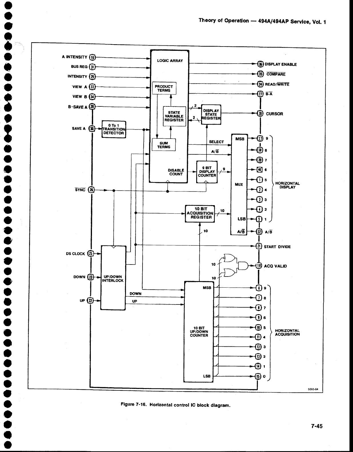
Theory
of Operafon - 494A/4g4Ap
Servlce,
Vol.
1
o
a
a
o
:
3
a
o
o
I
a
)
?
3
o
o
o
o
o
o
o
o
a
o
o
o
I
o
t
I
t
o
I
o
a
a
a
o
a
o
o
a
o
o
A INTENSITY
BUS
REG
INTENSITY
VIEW A
vtEw I
B-SAVE A
SAVE
A
1O BIT
UP/DOTYN
COUNTER
Theory
of Operation
- 494A/4g4Ap
Service,
Vol.
.l
Marker
lC. Marker
lC U9020
performs
several
func_
tions
on
the Horizontal
Digital
Storage
board:
In conjunction
with Horizontal
Digitat storage tc
U5020, it cr€ates
the
two waveform
markers
and
the
update marker.
Controls the processor
addresses
assigned
to digi-
taf
storage
-7A,78, FA,
and FB.
Creates
the fast-retrace
blanking
pulse
DSBLANK.
Takes control
of the address
lines to the display
RAM when
the microprocessor
accesses
the digit;l
storage
data.
To create
the
waveform
marker,
it monitors
the hor_
izontal
display
bits, HD0-9,
and
the
CURS and
B-A sig-
nals. When
these
lines
indicate
the
display has
reached
a point
that matches
on of hffo
points
previously
stored
in the lC by the microprocessor,
the lC sets
A INTEN_
SITY high, causing
U5020
to repeatedly
disptay
the
same
point
until
A INTENStry goes
low again
(which
it
does after a number
of DS ENBL cycles previously
stored
in
the lC by
the
microprocessor).
The update marker is initiated
by a comparator
detecting
that
the analog
sweep
and
the disptay
sweep
have crossed
as explained
elsewhere.
U3O2O
detecti
this event
on the CSLFS
line. lf the VALID tine
is high
when
this
occurs,
U3020 sets
INTENSITy
high,
causlng
U5020
to repeatedly
disptay
the same
point
untit 15
DS
ENBL
cycles
have
passed,
Then
INTENS|TY
goes
tow
again.
U3020
monitors
HD9 to generate
the DS BLANK
pulse. When
HD9
goes
from high
to low and
the
CUR-
SOR
line is low,
U3020 sets
DS
BLANK
high
for one
DS
ENABLE
cycle.
When
the microprocessor
wants
to read
valu€s
from
or write
data
to the waveform
memory,
it first
sends
a
starting
address
to u3020. circuitry on the vertical
Digital
storage
board
(A61A1)
controts
the
BUs GRANT
line which indicates
when U3020
can actually
access
the digital
storage
RAM without
disturbing
the disptay.
When
BUS
GRANT
goes
tow,
U9020
(instead
of U5020)
drives
HD0-9.
The Vertical
Digital
Storage
board also
generates
an
INCR
ADRS
(lncrement
Address)
pulse for each BUS
GRANT cycle. U3020 increments
the
address
that
it witl
assert
on HD0-9
by one
for each
INCR
ADRS
pulse.
The microprocessor
loads an initial address
and the
address register
outputs
are
applied
to tri-state
buffers.
Then,
the 10 bits of address
from the counters
are
butfered.
Those signals
are multiplexed
onto the HD
(horizontal
display)
lines
and
R/W
(read/write)
line
to the
memories.
These buffers are enabled
only during
the
bus grant portion
of the cycle
for display
of memory
7-46
data. At all other
times, horizontal control circuit
U5020
outputs
control the HD lines
to det€rmine
the memory
address
for update
of memory
data.
U3020 controls and subdivides the addresses
assigned
to digital
storage. The Vgrtical
Digital
Storage
board
responds
to addresses 7A,78, and FA. The Hor-
izontal
Digital
Storage
board
responds
to addresses
7A,
78, FA, and
FB. The DV
(Data
Valid)
line
(which
ctocks
data to or frorn th€ microprocessor
from
th€ instrument
data bus)
goes
to U3020, which sends
a controlled
ver-
sion of this line, VDV,
to the Vertical
Digital
Storage
board. When the addresses
on the Vertical
Digital
Storage board are to be addressed,
this line
is active
and none of the addresses on the Horizontal
Digital
Storage
board are affected. When
the addresses
on
the Horizontal board
are to be accessed.
VDV ls held
low by
U3020 regardless
of DV.
Address 7A
on
the Horizontal
board is further subdi-
vided
into 7A.0
through
74.7 by three bits
of 78 on
the
Horizontal
Digital Storage board. Access to these
addresses
is passed
between the two boards by
U3020.
Reading from address
FB will give
access
to the Hor-
izontal board regardless of which previously
had
acc€ss. Sending
the bits to 78 on the Horizontal
board
to access
7A.6
(DB6-4- 110) will pass
access
to the
Vertical
board. Sending
D86,5-11 to 7A.5 of the
Hor-
izontal board will also pass accesE
to the V€rtical
board. Sending
DB6,5-10 to 7A.5 of the Horizontal
board
will pass
access to the Vertical board,
but only
for one
DV cycle.
Tracking Digital-to-Analog
Converter. The 10-bit
digital-to-analog
converter operates as part
of the
loop
that acquires a binary
equivalent of th€ swP (sweep)
input signal from the Sweep
board. Gonverter U4040
accepts
the output from the 10-bit
up/down
counter of
U5020
and converts that output
to an analog current.
The analog current is then subtracted
from the SWP
signal (which is applied at edge connector
pin 60
through
buffer U40298).
The result of this
subtraction is
supplied
to up and down comparators in U3050.
This
creates
the UP
or DOWN signal,
as
appropriate,
to con-
trol the
count
direction
of the 1o-bit
up/down
counter
in
U5020. The counter then counts in the appropriate
direction, which changes
the digital-to-analog
converter
output
to reflect
the
proper
value.
Update
Marker Circults. These
circuits
create a cur-
sor to show
the present
update
location while a digital
storage
display refreshes.
The cursor is made by
stop-
ping
the
sweep for a short
period,
allowing the
crt
phos-
phors
to brighten
at that spot. This occurs
at each
of
o
o
a
o
a
o
t
o
o
o
t
a
?
o
o
o
o
e
t
t
a
o
o
o
a
a
O
o
o
a
I
o
o
o
a
o
a
a
o
o
O
t
o
o
o
o
o
t
o
t
t
o
o
a
:
t
o
o
o
I
a
o
3
a
o
a
o
a
t
o
o
o
o
o
o
o
I
o
a
o
o
o
o
o
a
o
o
o
the 500
digital
storage
sweep positions.
The
resulting
clisplay
appears
as a bright dot sweeping
across
the
crt,
rising
and
falling
with
the
signat.
The basic circuits
consist of a set of latches,
a
digital-to-analog
convert€r,
a compar"toi,
" pulse
gen_
erator,
and control
circuitry.
The Horizontat
Disptay
[iD)
data represents
thE ligital equivatent
ot the pi"ieni
update
position.
The latches cipture the data, and the
digital-to-analog
converter
{dac) converts it, creating
the analog horizontal
deflection signat. When the
swe€p
voltage
reaches-
the dac level,-the
sw€ep
stops
for a longer period
of time, and therefore
the crt is
brighter,
than at other sweep positions.
On the next
sweep,
the HD data increments
to the next position,
rnoving
the
cursor
along
the
sweep.
... Th" DSPL
EN (Disptay
Enabte)
signal
ctocks
the
HD
(Horizontat
Oata)
signats
into
latctres'Ul020
and
U2O3O.
The
tatch
outputs
drive
U2020,
a 1O_bit
oilitat+o_anatog
converter.
The
converter's
output
currenidrives
operai
tional amplifier
U4029A, producing
,a voltage called
HORIZ
StG.
When
a digitat
storagJsignat
is
disptayed,
HORIZ
SIG
drives
the
horizontat
O-eReciion
nmpliiier.
. Also,
U196-O
compares
HORIZ
StG
to
the
sweep
vol-
tage from U40Z9B. The comparator
output drives the
"Updat€
lnt€nsity.
input
on the Marker
tC, U30eO.
*re
tularker
tC Aenerates
" l-6_-g!it
putse,
ctocied
by DSpL
5N..Ll"_-ri:'.!g
edge
of U3O2O';
output
putse
produces
the INTENSITy
signal
that temporaiily
prevents
count-
ing by the g-bit display counter
'in u5020. This
effectively
stops
the
beam
for a short
time
ancl
causes
a
bright. spot (cursor)
on the trace to indicate
the horizon-
tal
point
being
updated.
Fast
Retace Blanking.
Between
the display
of the
B memory
contents
and display
of the
A m€mory
con-
tents, a fast
retrace
occurs,
This
retrace,
unlike
the one
that tollows the A memory display (cursor),
is not
required
to be seen and is blanke;. This is accom-
plished_
by btanking
control
flip_flop
U10148,
which
is
controll€d
by the most significant
bit of the rnemory
address
and
the DSPL
EN
signat
during
a marker
cycte.
. . Mernoriea.
Integrated
circuits
U1026
and
U2026
pro-
vide 8k bits of random
access
m€mory
for storage
of
tfie 1000
data
points
used
In
the digitalitorage
system.
Addressing
during
bus
transfer
of iremory
data
is con-
trolfed
by address
tri-state
buffers Ul}dg and U1016
and by horizontal
control lC U2095
during memory
update.
Theory
of Operaton - 4g4[l4g4fup
Service,
Vol. 1
DEFLECTION
AMpLtFtERS
(Diagram
27)
Refer
to the btock
diagram
adjacent
to Diagram
27
as well as the schematic
diagram. The Deflection
Amplifier
receives
vertical
signal
information
from the
vertical
section
of Digital
Storage
or the
Mdeo
proces_
sor, and horizontal
or sweep
voltage
from
the horizontal
section
of Digital
Storage
or the Sweep
board. Readout
data for the display comes from the crt Readout
cir-
cuits. Th€ output of the D€fl€ction
Amplifier
drives
the
crt deflection
plates. The amplifiers
contain
the switch-
ing circuits
necessary
to perform
th€ setection
functions
and they also contain
the amplifier
stages
needed
to
produce
the
deftection
plate
drive
signats.
Horizontal Section
Signal tines
HORTZONTAL
StcNAL (from
the
digitat
storage circuits through edge connector pin ag) -and
SWEEP (trom
the Sweep
circuit
through
edge
connector
pin
51) are applied
to switch
lC UZOSSA.
UZ0SS.
unOer
control
of the STORAGE
OFF signal (from
the digital
storage
circuits
through edge
connector
pin
7),
setects
either
the HORIZONTAL
STGNAL
or SWEEp
input.
The
SWEEP
signat
is setected
wh€n
the
STORAGE
bff tine
is floating
or putted
high. The
HORTZONTAL
STGNAL
is
selected
when
the line
is pulled
low. Resistive
divider
R7051
and R7081 reduces
the selected
signal
from
1 V/div
to 0.5
V/div. UZIT! buffers
the selectLd
signat.
It goes
out
to the HORIZ
OUT
rear-panel
connector
via
edge connector pin 48. UZoZ3
applies
the signat
to
switch
U70558. The HORTZ
R/O signat,
lrom the Crt
Readout
circuits,
is also applied
to U7OS5B.
The R/O
OFF signal, from the Crt Readout circuits selects
between
th€s€
two signals.
When
R/O
OFF is floating
or pulled high, the switch transmits
the signal
from
buffer
U7073
to the
shaper.
When
the
line is pulled
low,
it selects
the
HORTZONTAL
R/O
signal.
U70558
applies
the signal
to a shaper
network
to
comp€nsate
tor non-linearity
in the crt deflection
characteristics.
This network consists of resistors
R5059,
R5058,
R5057,
RS062,
R4061,
and
R4059,
ptus
diodes
CR1012,
CR4051,
CR4OS8,
and
CR4056. The
HORIZONTAL
POSIT|ON
vottage,
from the front panet
via edge
connector
pin 47, through resistor
R6032,
is
applied
to the shaper
circuit
so the shape
correction
factor
relates
to the crt deflection.
The shaped signal is then applied through
preamplifier
U2060
to the deftection
amplifier
circuits.
Horiz
Gain
adjustment
Rl0S5,
calibrates
th€ amount
of
gain
compensation
required
for proper
deflection
sensi-
tivity.
The horizontal
d€flection
amplitier
consists
of two
circuits
similar
to each
other,
one for each
horizontal
deflection
plate. One circuit
is an inverting
amplifier,
the
other
operates
in-phase.
Inputs
to e4oggA of the
invert-
7-47
Theory
of Operation
- 494A/494Ap
Servlce,
Vol. 1
ing sid€
ar€ through
the parallel
combination
of resis-
tors R4049
and
R4048
and
capacitor
C4057.
The series
connection
of resistor R4049
and variable
capacitor
C4057
provides
high-frequency
respons€ compensation.
Capacitor
C2A7 controls
high-frequency
feedback.
Input to the non-inverting
side is through
resistor
R5029
to the base of Q4025A.
R4019 and RS035
set
the dc level for the feedback
loop to the base ol
040258. Variable
capacitor
C5021
provides
adjustment
to set transient
gain. High-frequency
feedback
is con-
trolled
by capacitor
C3021.
Gain
of each
amplifier
section
is approximately
20.
(Horizontal
deflection sensitivity
of the crt is approxi-
matefy
21.3Vldiv per side.) Each section is singte-
ended
and incorporates
a gain-
degenerated
dual
pNp
transistor at the input
side
(for
temperature
compensa-
tion)
connected
as a differential
amplifier.
For
example,
Q40388 of the right deflection
amplifier
drives
emitter
follower
Q4047.
Signals with a low rate of change
drive
the output
transistor
through R5037
and
p3033.
As
the
rate
of rise
increases,
the drop across
R5037 increases
and when
it reaches
0.6 V, either
Q4035 or Q4042
are
biased on.
These
transistors
provide
the high
cunent
drive
for the
output
transistors. when the signal
rate of change
is
low, Q1043
drives the crt d€flection
plate
and e1o4g
provides
bias current for the amplifier. As the rate of
rise increases,
C3039
couples
the
signal
to the base of
Q1049. Q1049 provides the positive
drive to the
deflection
plate,
and
01043
provides
the negative
drive.
Each output
transistor
can
provide
a 200 V excursion
in
approximately
1 ps.
The
horizontal
amplifiers
operate with
approximately
1 mA ol bias
current
in the output
stage, as set by the
current
through resistor
R3031,
R1052, and R1049
at
the base
and emitter
of Q1049. Cunent
through resis-
tor R3031 also provides
the current
for the input
stage,
04038A/040388. Emitter follower e4042, operates at
approximately
2.5 mA. Resistors
R104S and R1034.
in
the emitter circuit
of Q1049 and
el043, degenerate
the
output stage for fast steps. Current
from the -15 V
source
through resistor
R4033,
sets the output
operat-
ing level.
Feedback
resistor
R3045 sets
this output
level
at approximately
142
V.
Operation
of the right-hand
(inverting)
section is
basically
the same
as th€ teft-hand (non-inverting)
sec-
tion.
Vertical Section
VIDEO
FILTER
OUT, from
the
Video
processor,
and
VERTICAL
SIGNAL,
from
the Digitalstorage,
are
routed
through switch lC U6055A, under control of the
STORAGE
OFF signal
from the Digitat
Storage
board.
7-48
Note that the vlDEo FILTER
ouT signal
ls bufiered
by
lC U7065 to prevent
a change
in load transients
from
aff€cting
th€ signal level. A high on the STORAGE
OFF
line
selects
the buffered
VIDEO
FILTER OUT signal,
and
a low selects
the VERTICAL
SIGNAL. U6065
inverts
the selected
signal and clamps
it to ground. Both
the
VIDEO
FILTER
OUT ANd
thE VERTICAL
S]GNAL
ArE
specified
at 0.5
V/div
with
0
V for the baseline and
posi-
tive voltages above
the
baseline.
The signal is re-inverted and offset by bufier U6073
so center
screen represents 0 V. Buffer
U6073
supplies
a sample of this cent€red
signal
to the rear-panel
VERT
OUT
connector
via edge connector
pin 46. The output
of U6073
is also applied
through
switch
U60558, when
the R/O OFF line is high,
to the vertical shaper
circuit.
When R/O
OFF
line is low,
the VERTICAL R/O
signal is
applied
to th€
shaper.
The vertical
section
shaper
(R4062,
R4065, R4067,
R4069, R4064, and CR4063, CR4064, plus the
preamplifier
U20621operates
the
same
as
the
horizontal
section. Q4078 limits positive
Excursions
to approxi-
mately one
division
above the top of the
scr€en
to pro-
tect the
output stages
from
being
overdriven.
The
vertical
output
stages are similar
to the
horizon-
tal stages, with the €xception of higher bias current.
Current
flow of approximately
1 mA, through resistors
R3089
and R3098,
produces
approximately
5 mA in the
output stag€s. To correct for the increased current in
the dual input stage transistors, Q408il and Q4101,
resistors R5081 and R5099
are lower value than
their
counterparts R5041 and R5027 in the horizontal
amplifier.
U6024 compares
the signal
level from the baseline
clamp, U6065,
with a reference l€vel set by divider
R7032/R7034.
This produces
the CLIP signal for the
Z-Axis
interfac€ circuits. When the
VIDEO FILTER
OUT
signal is rnore negative than the reference level
(approximately
1 division
above baseline),
it pulls
the
CLIP
line low.
R7021
pulls
the CLIP
line high if the sig-
nal
is more
positive
than
th€
reference level.
Z-AXIS AND
RF INTERFACE
(DTAGRAM
28)
The Z-Axis and RF Interface board
contains the
RF
interface circuits,
crt Z-axis drive
circuits,
power
moni-
tor circuits, and a timer that measures
operational
hours. This board provides
beam intensity
(nominally
from
the front panel),
baseline
clipping. and
unblanking
logic for the signals
or readout data. Unblanking
logic
comes from the Sweep board, the Crt Readout,
the
Deflection Amplifiers,
and the Digital
Storage.
The RF
Interface
circuits
receive data
from the microcomputer
that
controls
the
RF Attenuation, transfer
switch,
and lF
selection. A power
fail circuit on the board detects
any
o
o
a
?
o
I
a
o
o
)
a
o
t
o
o
o
I
I
I
o
o
a
o
a
o
o
t
o
a
o
I
o
a
o
I
o
o
o
I
o
o
o
o
o
o
o
o
o
o
o
o
o
o
o
a
o
o
o
o
o
a
o
a
o
o
o
o
o
o
o
o
o
o
O
o
a
I
o
a
o
O
a
o
o
a
a
?
O
change
in input
power
frequency
or power
supply
vol-
tage and notifies
the microcomputer.'
en etapiid time
meter is also located
on the board to give a indication
of total instrument
operating
time.
RF lhterface Circuits
The
RF interface
includes
the digital
control
circuits
that receive
the addr€ss
and instruition data from the
microcomputer
and
decode
it to control
the RF
Attenua-
tor, Transfer
Switch,
and
lF selection.
The
power
sup-
plies
.
that are required to drive the att€nuator and
switches
are
also
includ€d.
Address decoder U2045
latches the data at the
input of U3O46
whenever
the microcomputer
selects
address
4F. Table
7-7 lists the purpose'of
each
data
line
from the buffer.
Theory
of Opera{on - 494Ll4g4Ap
Servtce,
Vot.
1
the unblanking
gates, which furnish
cuffent to the Z_
Axis drive
amplifier
to drive
the crt control
grid.
The Z-Axis Drive Amplifier is an operational
amplifier
that consists
of transistors
e3047,
e4125,
and
04065. and retated
components.
R1OS0
is the input
resistance
for the amplifier,
and
R2066
is the
feedback
lej;is-tor.
The output is ctamped
by diodes CR3059
and
CR3066
to protect
the amptifier
from
transient
surges
in
case of crt arcing. The amplifier
is driven Oy two
sources,
exclusive
of each
other;
U203gBpzA42-drives
llt_e^^Tplifi€r during readout disptay periods, and
U2038A|O2O44
drives_ the amptifier' during sweep
display
periods. U2039
is an AND-NOR
gate
that pro_
vides_th€
logic
to one input
of NAND
gaie U2O38A
to
turn Q2044 on or off. The R/O OFF
line and the output
of U2039 must both be high for U203gA
to fumish
current
to Q2044.
Table
7€ lists th€ conditions
under
which
U2039
wiff
output
a high
to U2oggA.
Table 7-7
RF INTERFACE
LINES Table
7-8
U2039
TRUTH
TABLE
o1
Q2
o3
Q4
o5
Q6
o7
Purpose
Enables
10
dB
attenuator
No
connection
Enables
30
dB
attenuator
baseli
Enables
current
drivers
e2O2S
and
e302g
Enables
transfer
switch
driver
9.:1.""F _829
MHz
tF (high
state)
or 2022
MHz
lF (tow
state)
Enables 20 dB attenuator
U3046
output
(line
Q8)
CLIP
Z-Axis
Blank
Storage
Ofi
SWP
GATE
Gonditlon
000111000
When Q4 of U3046
goes tow, e2025 and e302g
conduct. This raises the Vcc of attenuator
drivers
U3034,
U3029,
and U30Og
to +16V for approximatety
100 ms to energize
the attenuator
solenoi'ds.
A diode
protects each attenuator
driver output line lrom the
inductive
voltage
surge
that occurs when the solenoids
change
stat€.
The
Transfer
Switch
operation
depends
on the out_
put of O302S/O9024. The e5 ouiput of U3046 is
applied to the input of operational
amptifier
U4O2g,
which
drives
differentiat
amptifier
O2025/O3O24.
When
Q5 goes high, Q3025
is biased
on and the Transfer
Switch
selects
the external
mixer. When
e5 goes
low,
Q3024 is bias€d
on, and
the
internat
mixer
is selected.
Diodes CR3018
and CR3017
protect the transistors
from voltage
spikes
induced
when
the Transfer
Switch
changes
state.
Z-Axis Circuits
The Z-Axis circuits provide
the drive
currents
and
bias voltage
to operate
the crt. They consist
of the
intensity
control logic cireuits,
which control
the crt
bearn current
for normal
signat
display
operations,
and
Only the combinations
shown
in Table 7-g plus a
high on
the RIO
OFF
tine
wiil
gate
a tow out
of U203gA.
When
the U2038A
output
is low, emitter
current
is fur-
nished to Q2044, which in turn furnishes current
through
R2051
(the
input
resistance
of the Z-Axis
drive
amplifier)
to Q3047.
U20g4B
is a single-shot
muttivibra-
tor that produces
a 3 micros pulse
to blank the crt
beam during
trace return,
between
readout
and signal
display.
The
other
source
of input
current
to the Z-Axis
drive
amplifier
is Q2042. This transistor
is turned on by
U20388
when
R/O
UNBLANK
is high and
R/O
OFF ia
low.
Ql028 is the current source for divider
Rl030iR1025
that establishes
the operating
point for
0.2042 and Q2044, which s€ts the intensity level.
Diodes
CR1045 and CR1
043, connected
from
the base
ot Q2042 and Q2044
to the emitter
ot eZ02Z,
timit the
dtsplay intensity.
These
diodes
prevent
the bases
from
going
more
positive
than
approximatety
0.6 v above
the
emitter voltage
of Q2022. This circuit,
which includes
lnt Limit
adjustment
Rl027, sets
the maximum
current
for both
Q2042
and
Q2055.
011
111
100
110
0
1
0
0
0
0
1
0
1
000
111
001
10r
000
7-49
Theory of Operation
- 4g4[l4g4Ap Servtce,
Vot.
1
Transistors
Q1017
and Q1015
provide
curr€nt
for
the trace rotation coil. Trace Rotation adjustment
Rl021 sets
the current
so the
displayed
trace
is aligned
with the graticule.
Power-Fail Detector
This
circuit
detects
an instrument
power
failure
and
transmits
th€
information
to the
processor
and
Memory
boards. The LINE TRIGGER
signat
from the powei
Supply board
through
edge
connector
pin
60 is supplied
to Q2011.
Q2011
buffers
the signat and
appties
lt to the
anput
of retriggerabte
on€-shot U20g4A. U2034A
per-
forms as a missing-pulse detector to generate a
power-fail
signal
through
O30l
l to notify
the processor
and Memory
boards
if more than two 60 Hz cycles are
dropp€d. To avoid
an undefined
state,
the output
from
U2034A is latched
tow
by
U2051.
Under normat
operat-
ing conditions,
the POWER-FAIL
signal from e3011 is
high.
Power-Supply Monitor
This circuit
detects
if one
or more of the
instrument
power
supplies
have
failed. Each voltage
supply
in the
instrument
is fed into
thick film
resistor
network
RgOSl,
which balances
th€ currents
to provide
a null output
(approximately
1
Vdc). Any line change
of more than
*,25oh
drives
the input to window comparator
U3OSI
beyond its *200 mV
threshold
and
generates
a low out-
put. 02059 and Q2067
drive the duat
tight emitting
diode DS1062
to provide
visual indication
of power-
supply status (grEen
indicates
normal operation
and
red
indicates a fault
condition).
The
output
of U3051 is also
fed to tri-state
buffer
U3052. After instrument
power up
or if a failure
is detected,
the microprocessor
will poll
address
CF to determine
power-supply
status over the
data bus.
Options Switch
Switch
S1010 works with switch S1050
on the
Memory
board
(A54)
to configure
the
firmware
for use in
various instruments
and
options. Settings
are
noted
on
the schematic
diagram. U3052
places
the switch
data
on the instrument
data bus at pow€r-up
as described
above
for th€ Power-Supply
Monitor.
Timer
An
electromechanical
timer,
Ml019,
is calibrated
for
a duration of 5000 op€rating hours. The current
through R1015
and
the
timer causes
the
copper
band
to
progress
along
the scale.
HTGH,VOLTAGE
SUPPLY
(D|AGRAM
29)
The High'Voltage
Supply furnlshes
the -3860 V crt
bias and 6.3 Vac filam€nt
voltage to the crt cathode,
and provides
dc restoration
for the Z-AXIS
DRIVE
sig-
nal. Th€ supply
consists
of four main
circuits:
1. The high-voltage
oscillator
circuit produces
the
crt filament
voltage and the 2@ vac that is stepped
up
and applied
to the
voltage
doubler circuit.
2. The voltage doubler circuit rectifies and filters
the high voltage for application
to the crt cathode.
3. The high-voltage regulator circuit samples
the
high voltage and regulates the op€ration of the
high-voltage
oscillator.
4. The Z-Axis clipper and rectifier circuits
couple
the
z-Axls DRIVE
signal to the
crt control
grid.
High-Voltage Oscillator
This circuit consists of transistor 01073,
transformer
T2065.
and associated components.
The
approximately
200
Vac, oscillator output is coupled
across T2065,
where it is stepped
up for application
to
the voltage
doubler,
and stepped
down for application
to the
crt
filament.
Voltage Doubler
The voltage
doubler
consists of CR4041, CR4035,
C4027,
C5021, C4024,
R3038, and R1039. The output
of the doubler is taken ofi the anode of CR4035
and
applied
to the
crt cathode
through the
filter consisting of
R3038,
R1039,
and C4024. Reference
voltage
for the
regulator is also taken off the end of R1039. R1039
keeps the filament
at
the
same
potential
as
the
cathode.
High-Voltage Regulator
This circuit consists of amplifier
U4083
and sur-
rounding components. The high voltage is applied
through
a voltage
divider
that consists of R1017B
and
R1017C. This voltage divider
is connected through
R1042
to +15 V. The sample
of the
high voltage
at pin
U is applied through
R4075
to the input
of comparator
U4083.
The correction
signal, in the
form of dc
drive,
is
applied as bias to Ql073
to set
the
oscillator current.
o
o
o
o
o
o
o
o
o
o
o
o
o
o
o
o
a
o
o
o
o
o
o
O
o
o
o
o
o
o
O
I
a
o
o
o
a
o
I
o
o
a
o
o
7-50
o
o
o
o
o
o
o
o
o
o
o
o
?
o
o
o
a
o
o
o
o
o
o
o
o
o
o
o
o
o
o
o
O
o
O
o
a
o
o
o
o
o
o
o
CR4078
and
CR40Z at the input
to U4ogil, protect
the input against
excessive
voltage excursions.
The
high-voftage
osciilator is protected
-Oy
enfteft RgOTg,
(d ?/
and
R4074
in case
the +i00 V suppi should
fait.
Nor_
mally,
CR1037
is back biased.
ti tne +t00V is not
present,
CR1037
conducts
and clamps
the input
nega_
tive;
the output
of U4093
swings
negative
ancl
e1073
remains
cut off. This circuit ensurei that e1073 witl
be.gin
to oscillate
only
after
the 100
V supply
r€aches
a
voltage
sufficient
to sustain
oscillation.
ChiOzZ (in
the
regulator
output circuit)
protects
the base ot OtOZg
from
excessive
negative
voltage.
Z-Axis Clipper
This circuit
consists
of diodes
CR1056
and
CR1046,
plus^associated
components.
The 22iyac trom pin i
of T2065
is coupted
through
C1O5g
and R104g
to the
junction
of GR1046
and CR.I0S6.
The regutator
circuit,
that consists
of VR1041,
R2050,
R2O4d,
and e204g
holds
the cathode
of CR1046
at approximatety
*100 V
to 143,V,
depending
on the setting
of R2040. CR1O46
and CR1056
ctip the incoming
2llyac. R2040
is
adjusted
to completely
cut-off
the crt with
Z-Axis
DRIVE
at minimum.
The
voltage
that passes
the clipper
circuit
is
coupled
through
Cl091 to the
Z-Axis
rectifier.
_ The clipped Z-AX|S DRTVE
signal is rectified
by
CR2044
and CR2046,
which are
1ne principte
com-
ponents
of the second section
of the Z-Axis circuit.
The
rectified
voltage
is then
fed to the grid of th€ crt.
Cl041 couples
the fast changes
of drive-voltage
to the
gl griO
to .speed
up the response
of the grid circuit.
Th€ crt ^gri^d ^is protected from high_voltage
arcs by
neons
DS20S2,
DS2054,
anO
D$2057. RlO43
protect;
CR2046
and CR2044,_
respectively,
from high-vottage
surges
if the crt should
arc.
cRT READOUT
(D|AGRAM
30)
The Crt Readout
assembly
stores readout
charac-
ters and generates
deflection
and Z-Axis signals
to
display
those
characters.
tt also
handles
the
frequency
dot marker
display.
Both
characters
and
frequency
dot
displays
are
time-shared
with
the spectrum
trace.
Generating
Readout
Crt readout
is handled
by sequential
logic,
clocked
at 3.41 MHz, supptied
by the piocessor Loard. The
readout
circuitry
(Figur€
7-17)
is composed
of the fol_
lowing
€lements.
1. Readout
On Timing _ RAM for character
storage.
Theory
of Operation
- 494A/4g4Ap
Servlce,
Vol.
1
2. Character
Count€r
- to acc€ss
the RAM and
control
the scan.
3. Character
Generator
- to unblank
the crt
b€am.
4, DIA
Converters
- to deflect
the crt beam.
5. Instrument
Bus Interface
- to store characters
and control the display. A more detailed block
drawing is provided
adjacent
to Diagram
30.
Forty characters
can be displayed
per line,
with
up
to sixteen
lines selected.
Normally,
up to three
lines
are displayed
while simultan€ousty
displaying
the
spec-
trum. When
over three lines
are to be displayed,
the
spectrum display is disabled to keep the readout
refresh
rate above
60 Hz.
Readout-On/Olf
Timlng. Characters
are written
one
at a time. This allows
a portion
of the spectrum
to b€
drawn between each character. Th€ character duty
cycle
is between
10%
and 257"
because
it varies
with
the character
drawn.
The
time
sharing
between
charac-
ter writing
and spectrum
display
is pseudorandom
to
reduce
the effect
of gaps in the spectrum
display
by
moving
them on
the trace.
The readout-off
time is set to 140
ps by one-shot
multivibrator
Ul055 (Figure 7-18). Ftip-flop
UtO41B
asserts
GEN RUNNING
after
ul055 tim€s
out, altowing
a character
to be drawn. After a character
is written.
ROW
0 COL 0 resets
the flip-flop,
which
clocks
off
time
one-shot
U1055. The ON control
bit must
have
been
asserted by the microcomput€r
to get readout
(as
described
under Instrument
Bus Interface
later
in this
section).
lf BLANK
(MSB
of
the
character
data)
is not set,
the
GEN RUNNTNG
flip-flop
unasserts
R/o oFF through
oR
gate U20448;
this switches
the readout
deflection
sig-
nals for the deflection amplifier
inputs (Diagram
271.
BLANK can be set by the microcomputer
to load a
space
into
the character
RAM so the readout
does not
use
time
for the
spectrum
trace
to scan
a blank charac-
ter.
Character Scan.
Although
the 8678
character
g€n-
erator
lC, U2048,
is often
used in raster
scans,
in this
application
it is used
to write complete
characters, as
shown
in Figure
7-1
9. A character
is drawn
as a pat-
tern of dots in an 8 x I matrix
wherE
the top row and
first three
columns
are blank. These
blank dots
allow
for beam retrace and spacing. The idle position
between characters
is indicated
on
the
figure.
7-51
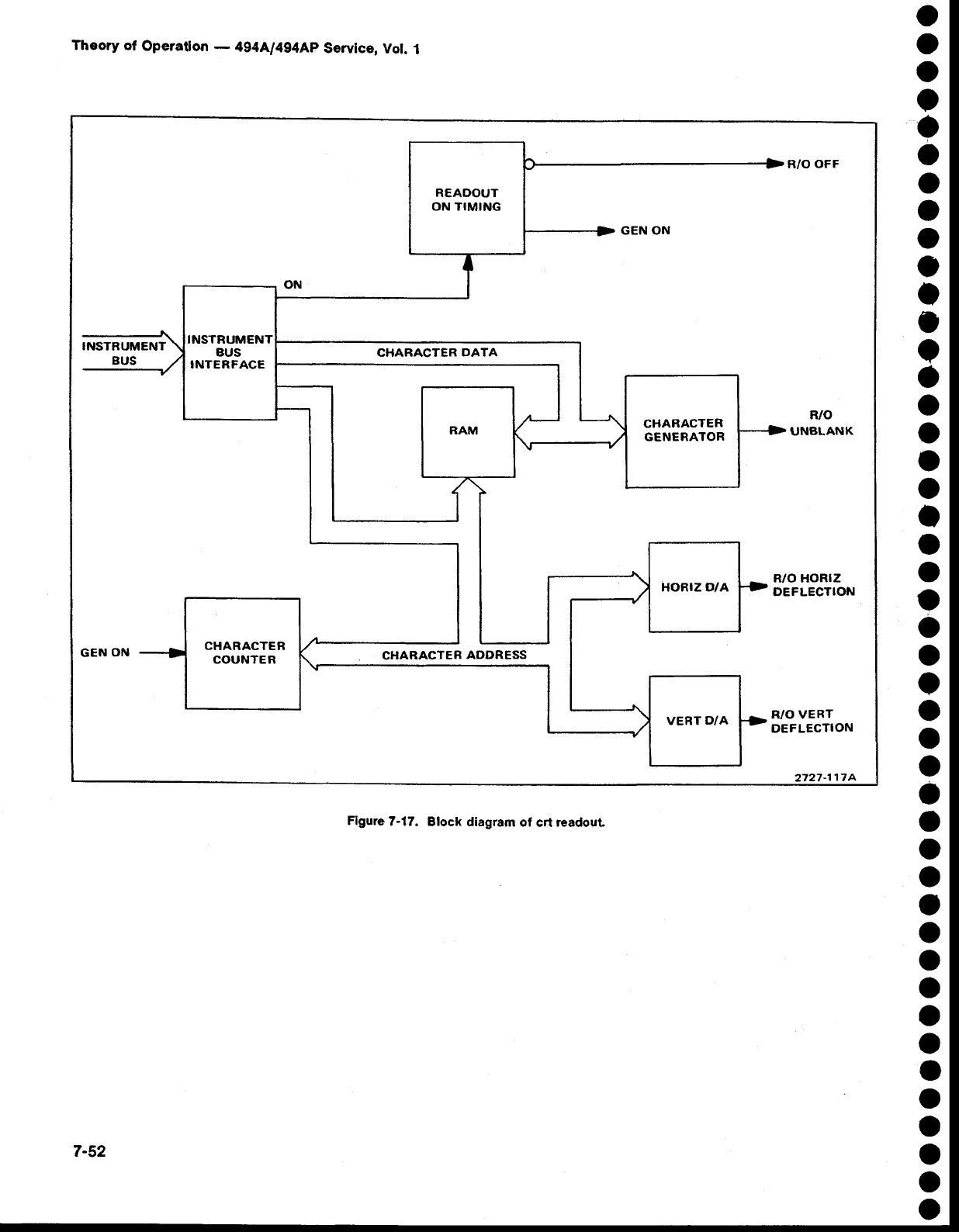
Theory of Operatlon - 4g4A/4g4Ap Service, Vol. I
READOUT
ON TIMING
CHARACTER
GENERATOR
CHARACTER
COUNTER
INSTRUMENT
BUS
R/O HORIZ
DEFLECTION
Flgure
7-17. Block diagram
ot crt
readout.
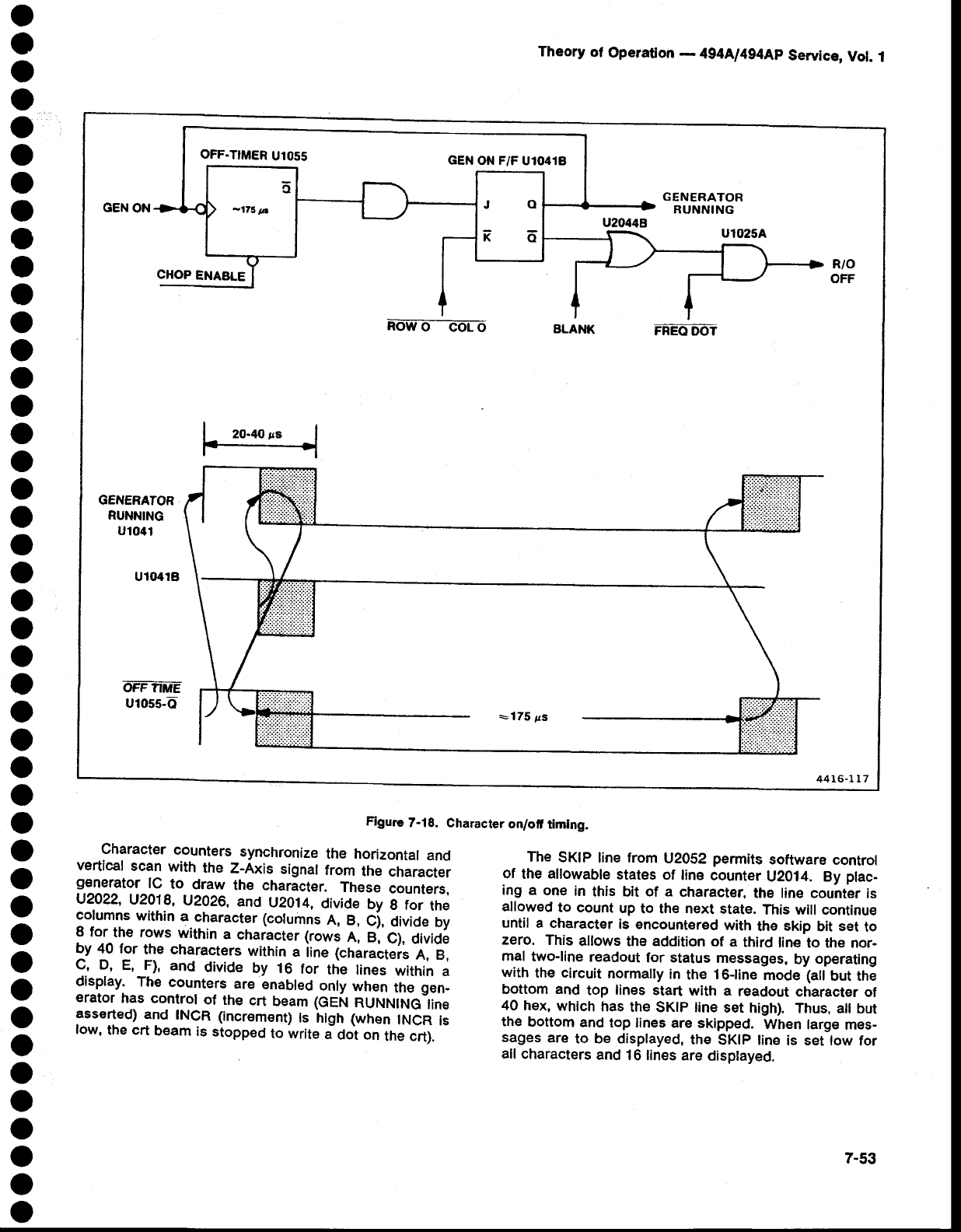
o
o
o
o
o
o
o
o
o
o
o
o
o
o
o
o
o
o
o
o
o
o
o
o
o
o
o
o
o
o
o
o
o
o
o
o
o
o
o
o
o
o
o
o
Theory
of Operation
- 4g4Ll4g4Ap
Service,
Vot.
l
Figure
7-18.
Character
on/of timlng.
Character
counters
synchronize
the horizontal
and
vertical
scan
with the Z-Axis
signal
from
the character
g€nerator
lC to draw the character.
These
counters,
U2022,
U2018,
U2026,
and U2014,
divide
by g for the
columns
within
a character
(columns
A, B, Ci, divide
by
8 for the rows
within
a chaiacter
lrows
A, e, C1,
OiuiO.
by 40 for the characters
within
a iine
lcharacters
A, B,
C, D, E, F), and divide
by 16 lor the lines
within
a
display.
The counters_
are enabled
only
when
the gen-
erator
has control
of the crt beam (GEil
RUNNING-line
asserted)
and INCR
{increment)
ls htgh (when
INCR
ls
low,
the crt beam
is stopped
to write
JOoi on
the crt).
The SKIP line from V2OS2
permits software
control
of the
allowable
states
of line
counter
U2014. By plac-
ing a one in this bit of a character,
the line
count€r
is
allowed
to count
up
to the next
state.
This will continue
until a character
is €ncountered
with
ths skip
bit set
to
zero. This
allows
the
addition
of a third
line
to the nor-
mal
two-line
readout
for status
messages,
by operating
with
the circuit
normaily
in the 16-line
mode
(all
but the
bottom and top lines start with a readout
character
of
40 hex,
which
has
the
SKIP line
set high).
Thus, all
but
th€
bottom
and
top lines
are
skipped.
When
large
mes-
sages
are to be displayed,
the SKlp line
is set low for
all
characters
and
16
lines are
displayed.
oFF-T'MER
U1055 cEN ON F/F U1041A
GEN
ON
R/O
OFF
FREO
DOT
I zo-co
u" I
lF-€,|
GENERATOR
RUNN!NG
u1041
u1(MrB
oFFTME
u1055-d
44t6-Lt7
7-53
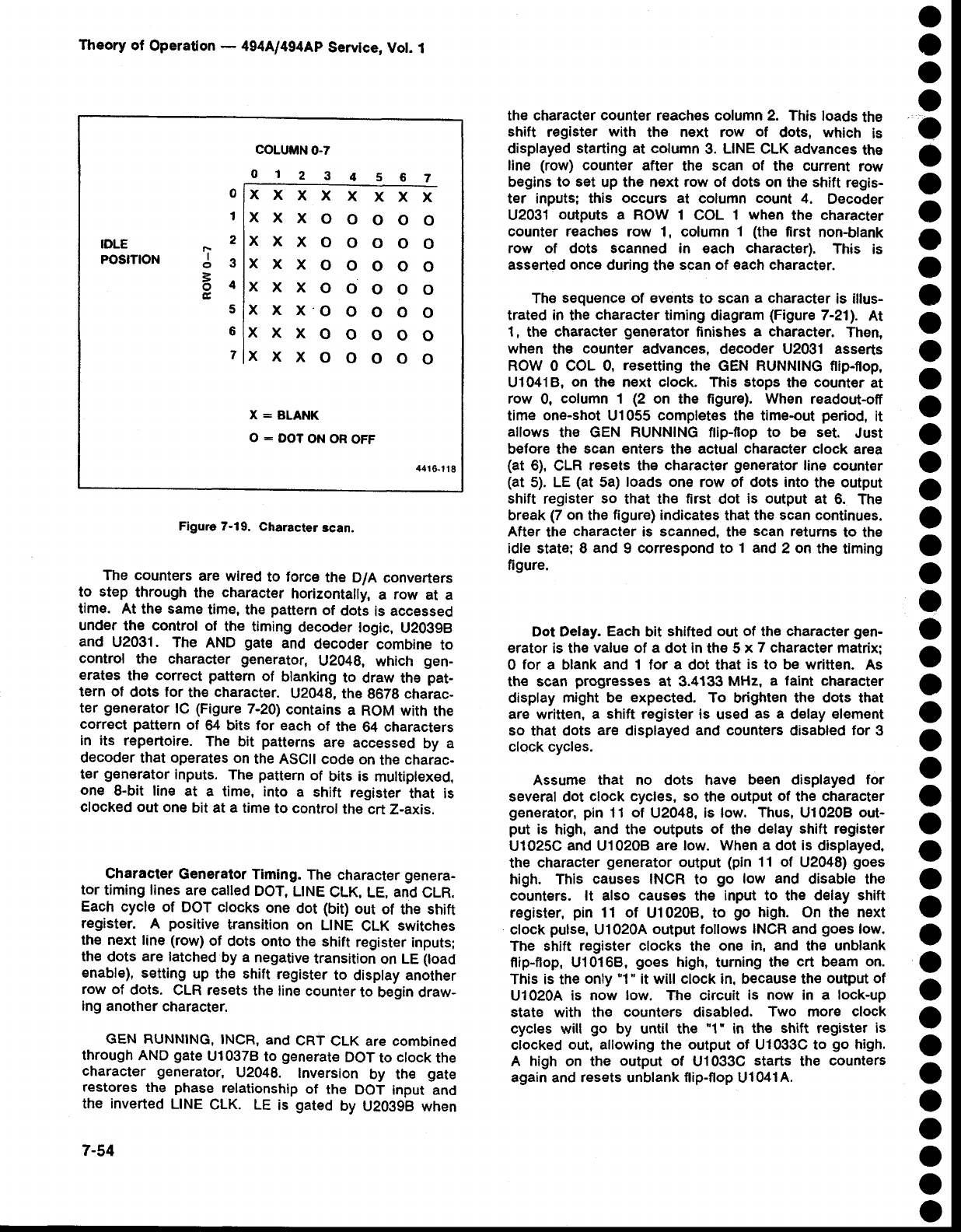
Theory
of Operation
- 494A/494Ap
Service,
Vot.
1
Figure 7-19. Charaeter
scan.
The counters
are wired
to torce
the D/A converters
to step through
the character
horizontally,
a row at a
time. At the
same
time, the
pattern
of dots
is accessed
under
the control
of the timing
decoder
logic,
U2O39B
and U2031. The AND gate and decoder
combine
to
controf the character
generator,
U2048,
which gen-
erates the correct pattern
of blanking
to draw th€ pat-
tern of dots for thE
character.
U2048,
the
8679 charac-
ter generator
lC (Figure
7-20)
contains
a ROM with
the
correct pattern
of il bits for each
of the 64 characters
in its repertoire.
The bit patterns
are accessed
by a
decoder
that operates on
the ASCII
code
on
the
charac-
ter generator
inputs.
The
pattern
of bits is multiplexed,
one 8-bit line at a time, into a shift register
that is
clocked out
one
bit
at a time
to control
the
crt Z-axis.
Character
Generator Timing.
The
character
genera-
tor timing lines are
called
DOT,
L|NE
CLK,
LE.
and
CLR.
Each
cycle of DOT ctocks
one
dot (bio
out of the shift
register. A positive
transition
on LINE CLK switches
the next line (row)
of dots onto
the shift
register
inputs;
the
dots are
latched
by
a negative
transition
on LE
(load
enable),
setting
up the shift
register
to display another
row
of dots. CLR resets
the
line counter
to begin draw-
ing
another
character.
GEN RUNNING,
INCR,
and
CRT
CLK are combined
through
AND
gate
Ul0378
to generate
DoT
to clock
the
character generator,
U2048. lnversion
by the gate
restores
the phase
relationship
of the DOT
input and
the inverted
L|NE
cLK. LE is gated
by u203gB when
7-54
the character
counter
reaches column 2. This
loads
the
shift register with the next row of dots, which is
displayed
starting at column
3. LINE
CLK
advances
the
line (row) counter after th€ scan of the current row
begins to set up the next row of dots on
the
shift
regis-
ter inputs; this occurs at column count 4. Decoder
U2031
orrtputs
a ROW 1 COL 1 when the character
counter reaches
row 1, column
1 (the first non-blank
row of dots scanned in each character). This is
asserted once during
the
scan of each character.
The
sequence of events
to scan
a character
is illus-
trated in the
character
timing
diagram
(Figure
7-211.
At
1, the character
generator
ftnishes
a character. Then,
when the counter
advances, decoder U2031 asserts
ROW 0 COL 0, resetting
the GEN RUNNING flip-flop,
U10418,
on the n€xt clock. Thig
stops
th€ count€r
at
row 0, column
1 (2 on the figure). When
readout-ofi
time one-shot
Ul055 completes
lh€ time-out
period,
it
allows the GEN RUNNING ftip-flop to b€ set. Just
before the scan enters the actual character clock area
(at 6),
CLR
resets
the character
generator
line
count€r
(at 5). LE (at 5a) loads one row of dots into the output
shift register so that the first dot is output
at 6. The
break
(7
on
the
figure) indicates
that
the
scan continues.
After
the character
is scanned,
the scan
r€tums
to the
idle state; I and
9 correspond to 1 and
2 on the timing
figure.
Dot Delay. Each
bit shifted
out of the character
gen-
erator
is the
value of a dot
in
ths 5 x 7 character
matrix:
0 for a blank
and 1 lor a dot that is to be written. As
ths scan
progresses
at 3.4133
MHz,
a laint character
display
might be expected. To brighten
the dots that
are written,
a shift register
is used
as a delay
element
so that
dots are displayed
and counters
disabled
for 3
clock cycles.
Assume that no dots have b€en displayed
for
several
dot clock cycles, so the
output
of the
character
generator, pin 11 of U2048, is low. Thus,
U1020B
out-
put is high,
and the outputs of the delay
shift register
U1025C
and
U10208
are low. When a dot
is displayed,
the character
generator
output
(pin
11 of U2048)
goes
high. This causes INCR to go low and disable the
counters. lt also causes the input to the delay shift
register,
pin 11 of U10208, to go high. On the next
clock
pulse,
U10204
output follows
INCR
and
goes
low.
The shift register clocks the one in, and the unblank
f,ip-flop, U10168,
goes high, turning
the crt beam
on.
This is the
only
'1" it will clock in, because th€
output of
U1020A is now low. ThE circuit is now in a lock-up
state with the counters disabled. Two more clock
cycles will go by until the "f in the shift register is
clocked
out, allowing
the output of U1033C to go high.
A high on the output of U1033C
starts
the counters
again and resets unblank flip-flop
Ul041A.
o
o
o
o
o
o
o
o
o
o
o
o
o
o
o
o
o
o
o
o
o
o
o
o
o
o
o
o
o
o
o
o
o
o
o
o
o
o
o
o
o
o
o
o
IDLE
POStTtON
0
1
2
J3
84
E5
6
7
COLUMN
0.7
01234567
xxxxxxxx
xxxooooo
xxxooooo
xxxooooo
xxxooooo
x x x.o o o o o
xxxooooo
xxxooooo
X: BLANK
O : DOT ON OR OFF
44r
Gl18
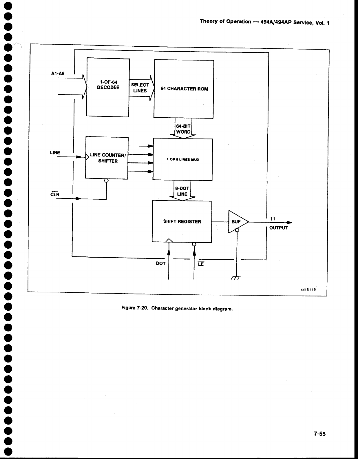
1-OF-64
DECODER 54 CHARACTER
ROM
LINE
COUNTER/
SHIFTER
SHIFT
REGISTER
Theory of Operation
- 4g4[l4g4Ap Servlce,
Vol.
1
Flgure
7-20. Character
generator
block diagram.
o
o
o
o
o
o
o
o
o
o
o
o
o
o
o
o
o
o
o
o
o
o
o
o
o
o
o
o
o
o
o
O
o
o
o
o
o
o
o
o
o
o
o
o
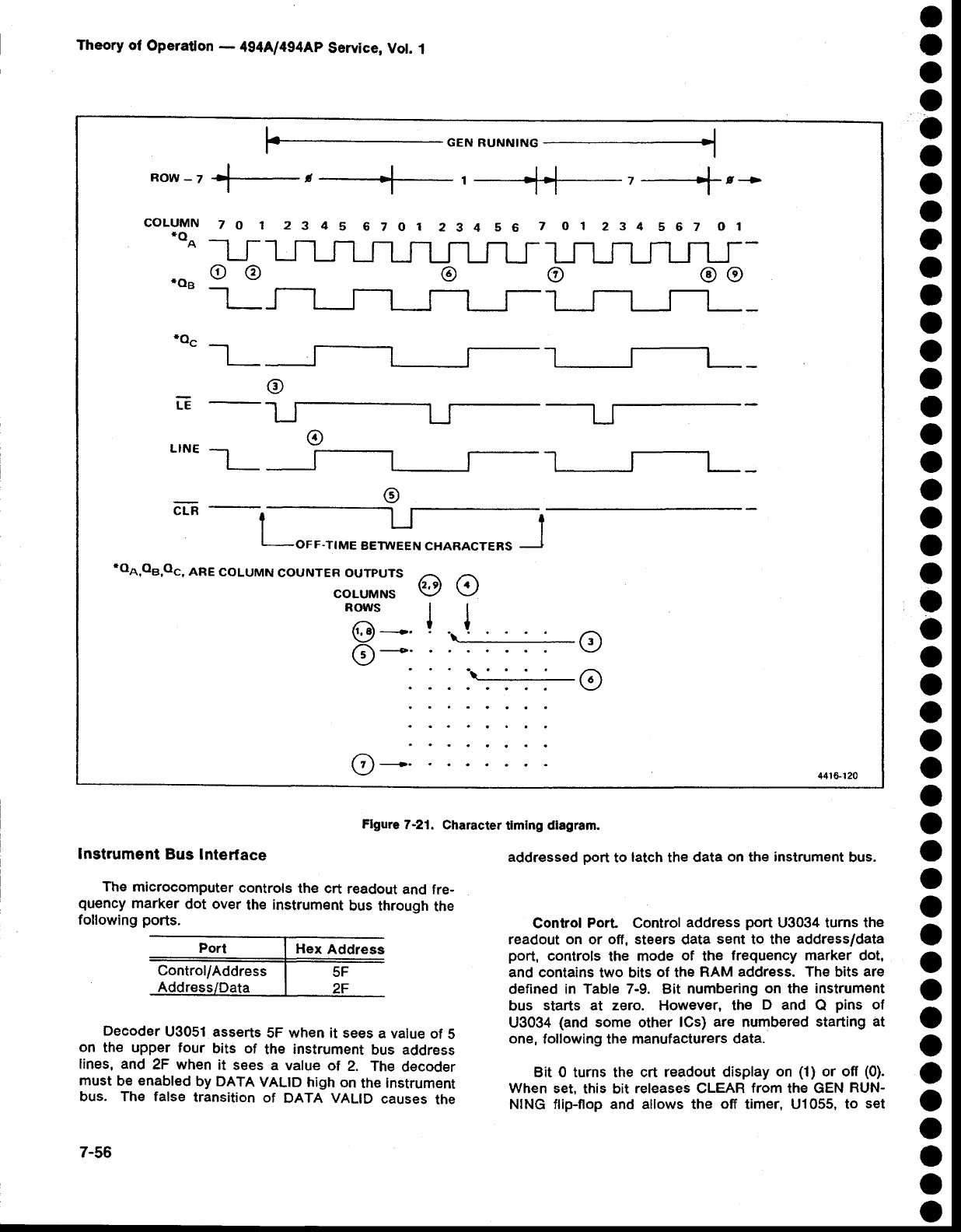
Theory of Operatlon
- 4g4A/494Ap
Service, Vot.
1
Flgure
7-21. Character
timing dlagram.
o
o
o
o
o
o
o
o
o
o
o
o
o
o
O
o
o
o
o
o
o
o
o
o
o
o
o
o
o
o
o
o
O
o
o
o
o
o
o
o
o
o
o
o
lnstrument Bus Interface
The
microcomputer
controls
the crt readout
and
fre-
quency
marker
dot over
the
instrument
bus through
the
following
ports.
Decoder
U3051
asserts
5F when it sees
a value
of 5
on the upper four bits of the instrument
bus address
lines, and 2F when
it sees
a value
of 2. The
decoder
must
be
enabled
by DATA
VALID high
on
the
instrument
bus. The false transition
of DATA VALID
causes
the
7-56
addressed
port
to latch the data
on
the
instrument
bus.
Conlrol
Port Control
address
port
U3034 turns the
readout on or off, steers
data
sent
to the address/data
port, controls
the mode
of the frequency marker
dot,
and contains
two bits
of the
RAM
address.
The bits
are
defined
in Table 7-9. Bit numbering
on the instrument
bus starts al zero. However, the D and Q pins of
U3034
(and
some other
lCs) are numbered
starting at
one,
following th€ manufacturers
data.
Bit 0 turns the crt readout
display on (1)
or off (0).
When
set, this bit releases CLEAR
from
the GEN
RUN-
NING flip-flop and allows the off timer, U1055,
to set
+GENRUNNIN
CoLUMN
to 1 2345 6zor 234 s6 7 or 234 562 ol
*oo ---'l r -1
LJ ru-
*oe
o @ @ o oo
-a_ m_
o
LE r-
o
L'NE-L- n-
@
roA,oB,oc,
ARE
coLUMN
couNTER
ourpurs @o
COLUMNS
ROWS | |
tl
@ +' ! '.1-:--------
A ---o.
Y/ ' '\i__:_'__' o
o
(7)---.
441S120
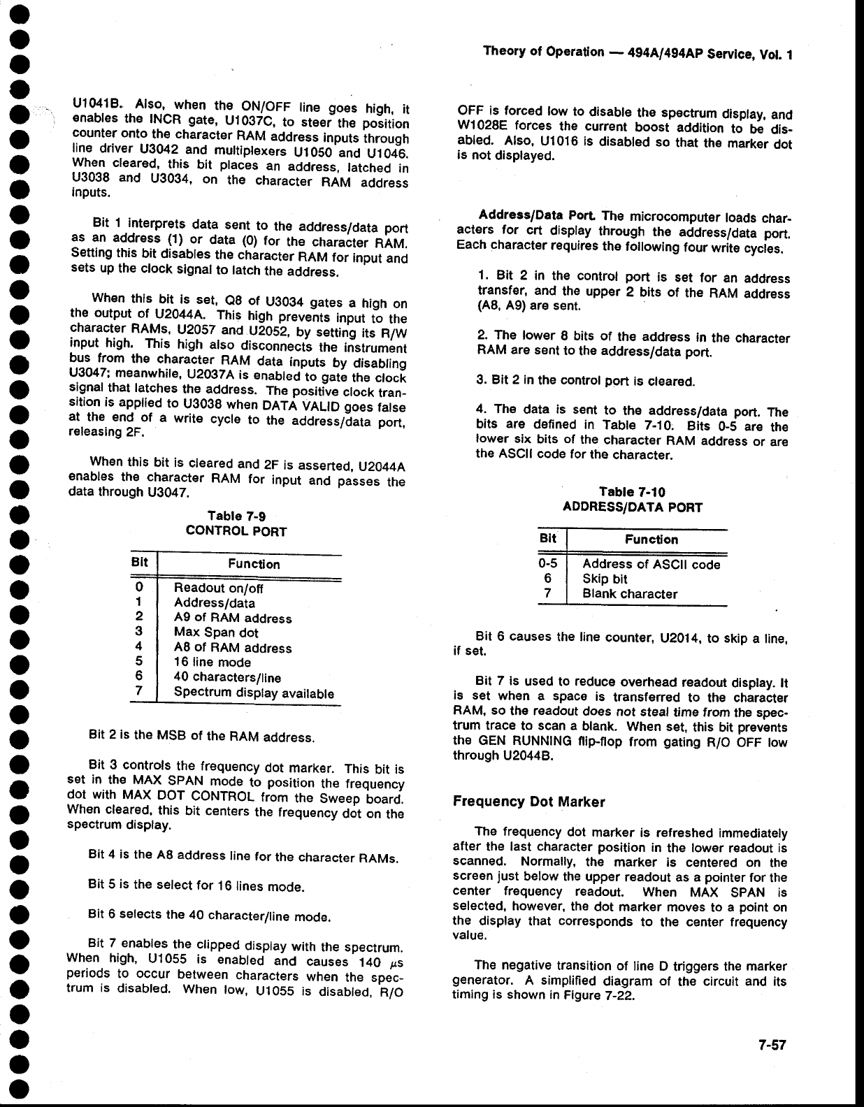
o
o
o
o
o
o
o
o
o
o
a
o
o
o
o
O
o
o
o
o
o
o
o
o
o
o
o
o
O
o
o
o
o
a
a
o
o
o
o
o
o
o
a
o
U10418.
Also, when
th€ ON/OFF
tine
goes high,
it
€nables
the |NCR
gate,
UlOgTC,
to steer-the
poiition
counter
onto
the character
RAM
address
inputs
through
fine
driver
U3042
and muttiptexers
UI050
and
U1046.
When
cleared,
this bit places
an address,
latched
in
U3038 and U3034, on the character
RAM address
inputs.
Bit 1 interprets
data sent
to the address/data
port
as an address
(1) or data (0)
for the character
RAM.
Setting
this
bit
disabtes
the character
RAM
for input
and
sets
up
the clock
signal
to latch
the address.
When
this bit is set, eg of U0034
gates
a high
on
the output
ot U2044A.--This
high preue-nts
input
to the
character
RAMs,
U20SZ
and U2052,
by setting
its R/W
input
high. This high atso
disconnecti
the instrument
bus from the character
RAM data inputs
by disabling
U3047;
meanwhile,
U2O}ZA
is enabled
to gate
the ctock
signal
that latches
the address.
The
positive
clock
tran-
sition
is apptied
to U3039
when
DATA
VALID goes
fatse
at the end of a writ€ cycle
to the addressldata
port,
releasing
2F.
When
this
bit is cleared
and
2F
is asserted,
U2O44A
enables
the character
RAM for input and passes
the
data
through
U3047.
Theory
of Operation
- 4g4[l4g4Ap Service,
Vol.
1
OFF is forced
low to disable
the sp€ctrum
display,
and
W1028E
forces
the current
boost addition
to be dis-
abled. Also,
U1016 is disabled
so that
the marker
dot
is not
displayed.
Address/Data
port The microcomputer
loads
char-
acters for crt display
through
the address/data
port.
Each character
requires
the
following
four
write
cycies.
1. Bit 2 in the control port is set for an address
transfer, and
th€ upper
2 bits of the RAM
address
(A8,
A9)
are sent.
2. The lower
I bits of the address
in the character
RAM
are sent
to
the
address/data
port.
3. Bit 2 in
the
control
port
is cleared.
4. The data is sent to the address/data
port. The
bits are defined
in Table 7-10; Bits 0-5 are the
lower
six bits of the
character
RAM
address
or are
the ASCII
code
for
the
character.
Table
7-10
ADDRESS/DATA
PORT
Function
Address of ASCII code
Skip
bit
Blank character
Bit 6 causes
the line
counter,
U2014,
to skip
a line,
if set.
Bit 7 is used to reduce
overhead
readout
display. lt
is set when a space
is transferred
to the character
RAM,
so the readout
does not steal
time frorn
the
spec-
trum trace
to scan a blank. When
set,
this bit
prevents
the GEN
RUNNTNG
flitrflop from gating
R/o oFF tow
through
U2O44B.
Frequency
Dot Marker
The frequency
dot marker
is refreshed
immediately
after
the last character position
in the lower
readout
is
scanned. Normally,
the marker is centered on the
screen
just
below
the upper
readout as a pointer
for
the
center frequency readout. When MAX SPAN is
selected,
however,
the
dot marker
moves
to a point
on
the display
that corresponds
to the center fr€quency
value.
The
negative
transition
of line
D triggers
the marker
generator.
A simplified
diagram
of the circuit and its
timing is shown
in Figure
7-22.
0
1
2
3
4
5
o
7
Table
7-9
CONTROL
PORT
Function
Readout on/off
Address/data
A9 of RAM address
Max Span dot
A8 of RAM
address
16
line
mode
40 characters/line
Spectrum display
available
Bit
2
is
the MSB
of
the
RAM
address.
Bit 3 controls
the frequency
dot marker. This
bit is
set in the MAX SpAN^m9de
to position
the frequency
dot with MAX
DoT CONTROL
from the Sweep
boarci
When
cleared,
this bit centers
the frequency
dot on the
spectrum
display.
Bit
4 is
the Ag
address
line
for
the character
RAMs.
Bit
5
is
the select
for
16 lines
mode.
Bit
6 selects
the
40 character/line
mode.
Bit 7 enables
the ctipped
display
with
the spectrum.
When
high,
U1055
is enabled
and causes.t40
ps
periods
to occur between
characters
when the spec_
trum is disabled.
When
low, U.l 05S is disabled.
R/O
7-57
Theory of Operaton - 494A/494Ap
Servicg Vot.
1
U1016A
delays
the
marker
dot to allow
retrace
white
gating DOT INV low to set up th€ disptay. DOT
tNV
afiects
th€ readout
deflection
outputs in the fottowing
ways.
1. The horizontal
output is connected
either to
ground,
for a center-scr€en
dot, or MAX
DOT
CON-
TROL,
for a max span pointer. MAX DOT
CON-
TROL is proportional to the center-frequency
readout offset from the center of the frequency
range.
2. The U10258 output goes tow during
the dot
interval
to cause
0301
I to insert an offset
current
Into th6 vertical
output, to shift th€ dot position
down
on the screEn.
3. R/O OFF is gat€d low to switch the d€flection
amplifier
inputs
from the Trace Mode
to the Readout
Mode, using the marker dot horizontal
and vertical
signals.
When the r€trac€ one-shot tim€s out aft€r about
5.9
ps, it's Q line triggers the unblanking one-shot
u10168,
which sets
R/o UNBLANK high for 5ps, via
DISPLAY MKR DOT through
U1G}7A. This refreshes
the
dot. DISPLAY
MKR DOT also holds DOT
INWL low
through
CRl013,
until the dot marker is drawn. Rl015
and G1011
slow the rise of DOT INTVL
to prevent
a
spurious
signal through the
'diode
AND'gate.
o
o
o
o
?
a
o
o
o
o
o
o
o
o
o
o
o
o
o
o
o
t
o
o
o
o
o
o
o
o
o
a
o
o
o
o
o
o
o
o
o
O
o
o
7-58
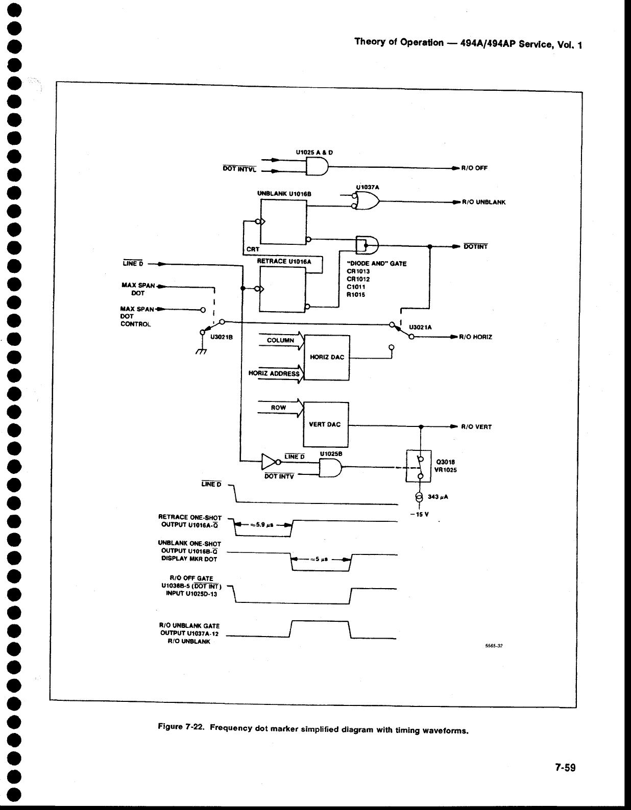
o
o
o
o
o
a
o
o
o
o
a
O
o
o
o
O
o
a
o
o
o
o
o
o
o
o
O
o
t
a
o
O
O
o
I
o
O
o
o
o
o
a
O
o
Theory
of Opera$on
- 494[l4g4Ap Servtce,
Vol. 1
Flgwe 7-22. Frequency dot ma.ker simprified diagram with timing waveforms.
___r- r
Fimvf +--i_-R/ooFF
"^foT*---r I
lla.x SPAN+------{ ,
.Dro{r€ Al{o" GAIE
cFr013
c81012
ct01 r
R1015
R€tn^cEoil€-sHor -r -tg'
ouTPururorse.O
F=s.grr
utraLANX
O|{E_SHOT
outpw urorea.o=
olSPlAY
lrr(R
DoT F=s rr
R/O OfF GATE
urorcas
166.Fifr?1
INPUT
U1O25D..I3
R/O UNBTANK GATE
ot TPUI u1037^-r2
n/o ur€LAXX
Theory of Operaton - 494A/494Ap
Service,
Vol. 1
The Frequency
Control section performs
the tuning
and scan
function
for the preselector,
l st LO, and 2nd
LO. lt also provides the sweep voltage for the
deflection amplifiers
in the Display
section
so the crt
display
is coincident
with the frequency
scan and
tun-
ing. This
section
contains
the following
major circuits.
Sweep
Circuits
on the Sweep
board
accept
trigger
inputs
from
line,
internal and
external
sources,
and
the normal
free-run
mode
of operation.
They
also
receive
external
horizontal and manual
sweep
inputs. The circuits
pro-
duce a PEN
LIFT
signal
for ehart
recorder
applications,
a SWEEP GATE signat for crt disptay btanking, a
SWEEP signalto drive
the crt beam across
the
horizon-
tal axis and drive
the horizontal portion
of the digital
storage
circuit.
plus
a ramp (OSC
SWEEP)
that is fed
through
the Span Attenuator
to the preselector
Driver.
the 1st LO
Driver,
and
the 2nd
LO.
Span Attenuator
This circuit attenuates
the ramp
signal as required,
to swe€p
the
frequency
of the
'lst and 2nd
tocal
oscilla-
tors, and tune the Preselector
so it tracks the center
frequency.
Center Frequency
Control
The Center
Frequency
Control
circuit
provides
a tun-
ing voltage
for the 1st and
2nd
Local
Oscillator circuits
that results in a linear
center
frequency
change as the
front panel
FREOUENCY
control
is changed.
The cir-
cuit is directly controlled
by the microcomputer,
so
remote control of the frequency
is possible,
by way of
the cPlB rear-panel
connector.
The COARSE TUNE
VOLTS
signal
from
this circuit
is applied
to the 1st LO
Driver circuits for summing
with the SPAN
signal
to
drive
the lst LO. The FINE
TUNE
VOLTS
signat is
applied
to the Preselector
Driver
for summing
with
the
lF Offset voltages, and
to the 2182
MHz
phase
Locked
2nd LO circuit for summing
with the 2nd LO SWEEP
signal.
l st LO Driver
The
1st LO Driver
performs
the following:
o Combines the COARSE
TUNE
VOLTS signat
with
the sPAN
signal
and
outputs
a current
to drive the
1st LO.
. Produces the tuning and sweeping
signal for the
Preselector Driver
circuits.
I Produces the mixer
bias
voltages.
o Produces a reference
voltage
that is used in both
the
1st
LO
Driver circuit and
the
Pres€l€ctor
driver.
o Produces a supply voltage for
the 1st LO.
Preselector Driver
The Preselector
Driver combines
the FINE TUNE
VOLTS
signal,
from the Center
Frequency
Control
board
with the PRESELECTOR
DRIVE signal and the SPAN
VOLTS
signal lrom the l st LO Driver.
This combined
signal is offset, to compensate lor the selected
l st lF,
then shaped so the Preselector tracks
with the lst or
2nd Lo as it is tuned by the output current. The
Preselector
Driver also drives the Filter
Select
switch
that selects either the Preselector or the Low-pass
Filter, depending
on
the
frequency
band
selected.
SWEEP
(Diagram
31)
The circuits on the Sweep board (A72)
provide
the
ramp voltage that drives the horizontal deflection
amplifier,
the l st LO Driver, the Preselector
Driver,
the
2nd LO, and
a voltage
used
to align
the
frequency
con-
trol system with the digital storage
marker
positions.
The sweep
board also provides
signals
for the Z-Axis
circuitry, an external
plotter pen,
and digilal storage.
The major
circuits on the
Sweep board
are:
o Sweep
Generator
. Trigg€r
Circuits
. Sweep
Control
o DigitalControl
o Marker
DAC
The sweep generator generates
the voltage
ramp
that drives the Deflection Amplifiers,
Digital Storage,
Preselector,
and the
swept oscillators.
The trigger
circuits
proc€ss
and multiplex the three
trigger
signals.
The sweep control circuit generates
the SWEEP
GATE
and PEN LIFT signals
and
determin€s
the
holdoff
time tor the sweep
generator.
FREQUENCY
CONTROL
SECTION
(Diagram
7)
o
o
o
o
a
o
O
o
o
a
o
o
o
a
o
o
o
o
o
O
o
t
o
a
o
o
o
o
o
a
o
o
O
o
o
o
o
o
o
o
o
o
o
o
7-60
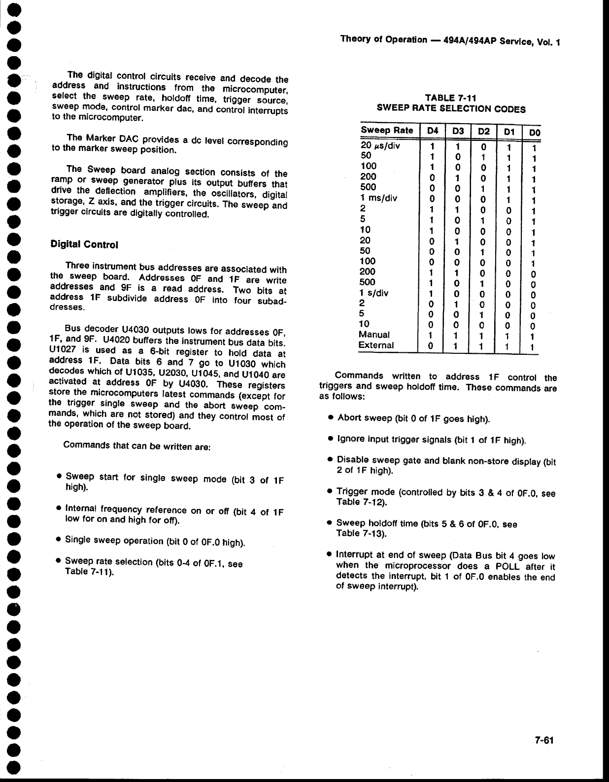
o
o
a
o
o
I
o
o
o
a
I
o
o
t
o
I
o
o
o
a
o
o
o
o
o
o
o
o
I
o
o
o
a
o
o
o
O
o
o
o
a
o
o
o
The
digital
control
circuits
receive
and decode
the
address and instructions from the microcomputer,
select the
.
sweep rate, holdoff time, trigger sourcer
sweep
mode,
control
marker
dac, and
cont?it
interrupts
to the
microcomputer.
.^.I"_I:rIT. DAC
provides
a dc levet
corresponding
ro
tne marker
sweep
position.
The Sweep board analog section consists of the
?Ip 9r sweep
generator
ptus tts output
buff€rs
that
drive the deflection amplifiers,
the osclllators,
digital
storag€,
Z axis,
and
the
trigger
circuits.
The
sweep
and
trigger circuits
are
digitally
controlled.
Digital Control
- Three
instrument
bus
addresses
are
associated
with
th€ sweep board. Addresses
0F and 1F are write
addresses
and 9F is a read address. Two bits at
addr€ss lF subdivide
address 0F into four subad-
dresses.
Bus
decoder
U40gO
outputs
lows
for addresses
0F,
1F,
and
9F. U4020
bufiers
the instrument
bus
data
bits.
U1027
is used as a 6-bit register
to hotd data at
address
lF. Data bits 6 and 7 go to U1030
which
decod€s
which
of Ui03S,
U2O3O,
UiO+S,
and
Ul040 ar€
activated
at addr€ss
0F by U4Og0.
ThesE
registers
store
the microcomputers
latest
commands
lexc-pt for
the trigger single sweep and the abort sweep com_
mands,
which
are not stored)
and
they
control
most of
the op€ration
of the sweep
board.
Commands
that
can be written
arE:
o sweep start for singte
sweep mode
(bit 3 of lF
high).
o Intemal
frequency
reference
on or off (bit
4 of lF
tow
for
on
and
high
for ofr).
o Single
sweep
operation
(bit
0 of 0F.0
high).
o Sweep
rate
selection
(bits
0-4
of 0F.1. see
Table
7-11).
Theory ol Operation
- 4g4[l4g4Ap Servtce,
Vol.
.t
TABLE 7.11
SWEEP
RATE SELECTION
CODES
Commands written to address 1F control the
triggers
and sweep
holdoff
time. These
commands
are
as
follows:
. Abort
sweep (bit
0 of tF goes
high).
o lgnore
input
trigger
signals (bit
1 of 1F high).
o 9islble sweep
gate
and
btank non-store
disptay
(bit
2 of 1F
high).
o Trigger
rnode
(controiled
by bits
g & 4 of 0F.0,
see
Table
212).
. Sweep
holdoff
tim€
(bits
5 & 6 of 0F.0, see
Table 7-13).
. Interrupt
at end
of sweep
(Data
Bus bit 4 goes
low
when the microprocessor
does a pOLL after it
detects
the interrupt,
bit 1 of 0F.0 enables
the end
of sweep
interrupt).
Sweep Rate D4 D3 D2 D1 DO
20
ssldiv
50
100
200
500
1 ms/div
2
5
10
2A
50
100
200
500
1 s/div
2
5
10
Manual
External
1
1
1
0
0
0
1
1
1
0
0
0
1
1
1
0
0
0
1
0
1
0
0
1
0
0
1
0
0
1
0
0
1
0
0
1
0
0
1
1
0
1
0
0
1
0
0
1
0
0
1
0
0
1
0
0
1
0
1
1
1
1
1
1
1
1
0
0
0
0
0
0
0
0
0
0
0
0
1
1
1
1
1
1
1
1
1
1
1
I
1
1
0
0
0
0
0
0
1
'l
7-61
Theory
of Operation
- 494A/494Ap
Service,
Vol. 1
Tabte
7-12
TRIGGER
SELECTION
MODES
Trigger
Mode
Free
run
Internal
Ext€rnal
Line
Table
Z-13
SWEEP
HOLDOFF
SELECTION
Sweep Holdoff
Short
Medium
Long
Sweep Generator
The
sweep
generator
is an integrator
circuit
consist-
ing of operational
amplifier
U10S5 with one fixed and
two switchable
capacitors
in the feedback
circuit. Fixed
capacitor
C1061 is used for the faster sweep rat€s.
The other
two capacitors,
C1065 or C1062,
are added
to change the time constant when either e2069 or
Q2064 are switched
on by comparators
U1060A or
U2050A. These comparators
are driven by register
U2030,
which interfaces
to the instrument
bus. For
manual sweep
operation,
02060 is turned
on and the
integrator
becomes
an amplifier.
Multiplexer U3060 connects timing resistors
between
a -12 volt referenc€,
out of UO050B, and
the
input
to integrator
U2060.
Data
bits D2,
Dg, and
D4 of
address
0F.1 drive
the sElect
inputs
of the multiplexer.
The voltage reference
of -10 volts out of U4055
is
boosted to -12 volts
by
U30S0B.
A voltage
divider sets
the
non-inverting
input
of U1055
to -g volts. Therefore,
there is about 4 volts
difference
across
the timing resis-
tors. The timing
current
through
the resistors
varies
over
two decades such
that 1/l is proportional
to a 2-5-
10 sequence.
Switching in feedback
capacitors
C1065
and
C2060
each changes
the
sweep
rate by a factor of .l
00
times.
Sweep Accuracy adjustment,
R1062,
compensates
for
differences in timing voltage
or timing circuit
values.
The
timing
capacitors
ar€ match€d
so that one
adjust-
ment compensates
for small
variations
in each set.
Trigger Circuits
The sweep
circuit can be triggersd
by an extemally
applied
signal, the int€rnal
video filter slgnal, or from
the power
line. Each
trigger signal is converted
to TTL
level
and then
applied
to trigger multiplexer
U2026,
part
of the trigger control circuit. The trigg€r control circuit
selects th€ desired triggering signal and triggering
mode or rejects
th€ trigger to let the sweep circuit free
run, be manually
controlled,
or let the external sweep
mode
be used.
An external
trigger signal applied
to the external
HORIZrrRIG connector
is converted
to TTL level by
02030. CR2030
limits any voltag€ surges
that may be
on
the
line. Line trigger signals,
from
the
power
supply.
are applied through comparator U3025A
to the multi-
plexer. Video
Filtsr
Out
signals
from
the
Video Proces-
sor board are buffered
by Q4037
and
converted
to TTL
level
by
03030. Both
the external and video
trigger sig-
nals are applied to multiplexer
U2026 through
Schmitt
trigger inverters in
U1015C.
Under
control of the data (D2 ancl
D3) from register
Ul035 (at
extended address
O
of address
0F),
the
multi-
plexer
sel€ots the
trigger
signal and
passes
it to flip-flop
Ul0168.
After
retrace and holdoff
time, Ul0168 allows
a trigger to pass through V2026 and U2020C
to r€set
the Sweep
State
Control
flipflop U1025. When U1025
is reset
the
integrator starts a n€w
sweep.
Sweep Output Circuits
The sweep ramp from the integrator is applied
through
buffer
amplifiers,
U3045
and
U4050,
and a bus
on the Mother
board
to the Deflection Amplifiers,
Span
Attenuator,
and Digital
Storage board.
The sweep out of
U3045
is an
11 volt
peak-to-peak
ramp centered
around
0 voft. The sweep out of u4050 is a 22 volt peak-to-
peak
ramp for the
oscillators.
The sweep signal also drives pen-lift
comparator
U3010A
and the end-of-sweep comparator
U30108.
The threshold
for the pen-lift
comparator
is +7.4 volts.
The threshold
for the end-of-sweep
comparator
is +8
volts. The sweep ramp, from the integrator,
starts at
-8 volts and
rises
towards
+8 volts. When the signal
reaches
+7.4 volts, th€ p€n lift comparator
toggles.
This output is gated
through u30158 and the pen lift
signal
goes hlgh. When
the sweep ramp reaches
+8
volt, the end-of-sweep comparator,
U301 08, toggles.
The resultant
low output
is applied
through U1015A
to
become
the
EOS
(end-of-sweep)
signal.
o
o
O
o
o
o
O
o
o
o
a
o
o
a
o
o
o
a
o
o
o
o
o
O
o
o
o
o
o
t
o
o
o
O
o
o
o
o
o
o
o
o
o
o
7-62

o
o
a
o
a
o
o
o
o
O
o
o
o
a
a
o
a
o
I
o
o
o
o
t
o
o
a
o
O
I
o
a
O
o
o
o
o
o
o
o
o
o
o
o
Marker DAC
The Marker DAC circuit provides a dc level
corresponding
to the marker sweep position. This
occurs during retrace.
allowing
osciliators
to operate
long
enough
for the counter
to get an accurate
reading
gJ the marker position. The processor
loads
twelve
bits
to Marker
DAC
UlO47. Thls
dc level
reptaces
the
swe€p
ramp
during
th€
during
the
retrace
time
when
the
swe€p
is inactive.
The
Marker
circuits
on
the
Horizontal
Digital
Storage board reads the dc voltage
and recon-
verts
to digital
to feed the processor.
ihe processor
compares
these bits to the location
of the marker
in
digitar
storage
and
adjusts
the
Marker
DAC
bits untir
the
digitized
voltage
matches
the
marker position.
U1047
is a 12-bit
DAC. The 12 bits come
frorn
registers
Ul040 and
Ul045, the address
0F
second
and
third
extended
address
registers.
The
DAC
produces
a
current output, which U2040 converts
to a voltage.
U2045
sums
an offset
voltage, giving
a voltage
range
of
about
*9 volts. This
voltage
range
is greater
than
the
range
of the sweep
ramp. This
fact,
and
the DAC
hav-
ing
twelve
bits
guarantee
that there
will be a twetve
bit
number
for the DAC
for each
of the 1000
digital
storage
points.
Sweep Control
U1025A
is the Sweep
State
Control
flip-flop.
When
reseti
the high
at the
Q(bar)
output
turns
off
FET
01062
and allows
-the
integrator
capacitors
to charge.
When
the
sweep
state control
ftip_flop
is set,
by a iow
on pin
4, its
Q(bar)
goes
low. This
switches
the
output
of corn_
parator U10608 so its output turns e1062 on and
9j:!!lln"" the timing
capacitors.
The
e(bar)
output
of
U1025A connects
to pin 5 of Ut017A so this low
switches
the output pin 6 to its high
impedance
state
(its
output
is open
coltector).
The
Q outpui
of U1025A
is
high. Both
U10t6A
and U,t0168
wheie previousty
set
when the Q output was low. This staris lhe holdoff
cycle
or retrace
time
which
is described
in
detail
further
on.
The
Sweep
State
Controt-flip.flop
Ul025A,
is set by
a low out of NOR gate U2O20A
when
either
the EOS
{end-of-sweep)
or the ABORT SWEEP
tines
go high.
ABORT
SWEEP
is gen€rated
when
a 1 is written
to b0
at address
1F. The
Sweep
Control
flip-flop
is reset
by
either
a trigger
signal
from multiplexer
V2026
or a hioh
on the MNL or EXT SWp line. The microcorputlr
writes
to bits D2
and
D3
at subaddress
1 of address
0F
for
the manual
or external
sweep
mode.
Theory
of Operation
- 4g4Al4g4Ap
Service,
Vot.
.l
Trigger Control
A sweep
is initiated
by the microcomputer,
in single
sweep
or manual
mode as noted abov€, or by one of
three trigg€r signats
selected
by
the multiplexei
U2020.
Oata
bits D2 and D3 at addrEss
0F.0
select
the input
trigger signals and rout€ tham to the clock input of
U10168.
During
swe6p
time
thg flipf,op
U10168
is
set
by a low on
th€
Q
output
of U1025A.
The high on the Q(bar) output
of u1025A is atso
applied
through an inverter buffer in U1O17A.
The
resultant
low out discharges
holdoff
capacitor
C3032
at
the input
to u30258. The output
of u30258 is tow so
the output of NAND gate u1020D is high. Ftip-flop
U10168
requires
a high-to-low
transition
to ctock
any
input
through.
Since
lt is high, incoming
trigg€r
signati
will
have
no efiect
on
the circuit.
At the end of sweep, the e(bar) output of U1025A
goes low. This s\witches
the output
of U1017A
to its
high
impedance
state and
tha holdoff
capacitor,
CgOg2,
starts to charge towards +15 volts through RgO30.
When it reaches +5 volts the comparator output
switches
high. This, along with a high on pin 13 of
NAND
gate
U1020D,
causes
the output
to go low and
the
high-to-low
transition
clocks
U2026 so the incoming
lrigger signal
can now clock U10168
and produce
;
high
at the
Q(bar)
output. This
is gated
through
UZO26
to the input ot u2020c, so the output
of the NoR gate
will now reset the Sweep State Control flip-flop,
U1025A,
and start
a new sweep.
In the free-run
mode
the multiplexer
U2026, selects
the +5 volts
on pin 5. This
high is clocked
through
to
the sweep state control flip-flop immediatety
after
retrace.
fncoming
trigger signals
are ignored
and the
sweep
runs
automatically.
In single
sweep
mode
the sweep circuit
cannot
be
re-triggered
until
it is armed
by the
microcomputer.
Bit
D0
is set
high
at subaddress
0 of address
0F
(U1095-6).
This appears
as a high on pin 2 of U4010A. Since
U1016A
has been
set by the previous
sweepr
the two
highs
at the input
produce
a low at pin 13 of Ul020D.
Therefore,
incoming
triggers are
disabted. The sweep
is
now
in an
idle
state and
cannot
run until
the microcom-
puter
arms
the
trigger
circuit
again.
This is done
by
set_
ting bit D3 high
at address
lF, which
produces
a high
out of U1026
pin 3 and clocks
flip-flop
Ut0t6A. The
resultant
low
at pin
1 of u4010A forces
a high at pin
11
of U1020D, and
arms
the trigger
circuit. Thus
a signal
can
now trigger
the sweep circuit
and
the
singte
sweep
cycle
repeats.
7-63
Theory
of Operatlon
- 4g4A/4g4Ap
Service, Vol.
1
Sweep Holdofr
During
retrac€,
the sweep must b€ held off long
enough
for the timing capacitors
in the integrator
to
discharge
and
the circuit
to stabilize.
To prevent
flicker,
the holdotf
period
must
vary as sweep
tim€ changes.
U30258 and
three
timing
capacitors (C3027,
C3030, Lnd
C3032)
plus
a resistor (R3030)
form
the
hotdoff
circuit.
During
sweep
time pin 5 of U1017A is high.
This
pulls
pin 6 low and discharges
Cg0g2. During
retrace,
pin 6 is released
and the timing capacitors
start to
charge. When they reach *5 V comparator Ug025B
toggles and its output goes
high. This, along
with
th€
high
on pin 13 of the NAND
gate
U102OD,
provides
the
clock
pulse
for U2026
to pass
a trigger signat
through
to the Sweep
state
controt,
u1025.
lnterface Circuits
ln addition
to the sweep
circuits,
there are circuits
that interface between the microcomputer
and the
Reference
Lock modul€.
These circuits generate
an
interrupt
(SER
REO)
when a change
of status in the
Reference
Lock modute
occurst
respond
to the POLL
routine, and provide
data so the microcomputer
can
monitor the status
of the Relerence
Lock module.
To determine
the status of the Reference
Lock
module, the microcomput€r
reads
the status
of bits 0
and 1 (DBo & DBl) of the data bus at address
9F.
These two bits connect through tri-state buffers in
u4015C to th€ |NTL REF and (REF
LOCK)(bar)
tines
from the R€f€rence
Lock
module.
The
INTL
REF
line is
high when the internal
rEference
is used and low for
extemal referenc€. The {REF
LocK}(bar) goes high
when the 3rd LO is not locked to the frequency
refer-
ence
and low
when
it is locked.
When
address
9F is read, U2O1Z
is enabled
and
latches
the (|NTL REF)(bar)
and REF LOCK signals.
Thus,
the
bits
on pins
1,2,
and
5,6, of the
exclusive-nor
gates
in U2015
match
each
other. The open-collector
outputs are wired together,
so when the outputs
are
high, inverter
U10178
applies
a
low
to the clock
input
of
flip-flop
U2025A.
When
a change
in status
occurs,
one
of the bits to the exclusive-nor
gates
(pin 1 or pin 5)
changes. There
is now
a difrerence
between
the
present
status and the previous
status,
stored
in U201 7. One
output
of U2015
now switches
low and a low-to-high
transition
occurs on the clock pin of U2025A. This
triggers
an interrupt
and causes
the microcomputer
to
inquire about
the new status. Reading
the new status
activates
the latch and resets
the circuit. Transistor
Q3015,
driven
by bit D4
at address
1F,
turns
the INTL
REF
(internal
reference)
on
or off.
The Interrupt and
Service Request
circuit
gensrat€s
the instrument
bus interrupts
and responds
to the sub-
s€quent
poll routine from the microcomputer.
There
are
two sources of an interrupt from the sweep board,
either an EOS (end-of- sweep) has occurr€d or a
change of status of the reference
lock module is
detect€d. When
an EOS
occurs, and
provlded
the EOS
Interrupt Enable bit is high, the flip-flop
U1010A is
clocked and its Q(bar)
goes low. This produces
a high
out of u1020B
which
turns
Q4032
on
to pullthe instru-
ment bus line SER REQ (servic€ request)
low and
forces an interrupt.
The microcomputer response
to an interrupt
is with
a poll routine, lt first writes FF to the instrument
address
bus. The Sweep
board address
decoders
nor-
mally
r€spond
only
to addresses
0F,
lF, and
9F, but
the
interrupt
circuit detects when
bit 7 of the address
bus
(AB7) goes high.
The microcomputer
rais€s
the POLL
line and reads
the instrument
data bus.
The output
of
U2010A
goes low. This. anded with the low out of
U10104,
generates
a high
to turn 03020
on and
pull
bit
DB4 of the instrument
bus low. When the microcom-
puter
reads a low on bit DB4 it lowers
the POLL
line
and writes 7F on the instrum€nt
bus. Again, none
of
the
other
decoders respond. However,
bit
7 (AB7)
of
the
address
is pulled
low. The microcomputer now
writes a
word to the data
bus with all bits sxcept
bit DB4
high.
This acknowledges
the interrupt. The microcomputor
now
raises
the
POLL line again
and
since
both
inputs
to
U20108
are high,
the output of the
gate goes
low. The
POLL line is then
pulled
low and
the
low-to-high
transi-
tion clocks
the
low
on
the D input
of U10108 through
to
reset
u1010A.
lts Q output
then
sets
u10108.
04032
is cut off, the interrupt
is removed, and the circuit
is
now ready
for another EOS.
A change-of-status in the reference
lock module
causes a low-to-high
transition
on the clock input of
u2025A
to latch the Q (pin
5) output high and
the o(bar)
output
low. This low is gated
through U10208 to turn
04032
on, and
pull
SER
REQ
line low. When
the
micro-
computer responds, by writing FF
and
raising
the
POLL
line, U2010A
output goes low, however,
at this time
U202OB output
goes high,
because
of the
low on
pin
6
of U2025A. This turns 03025 on and bit DB7 on the
instrument
bus goes low. The microcomputer
reads
this and pulls
the
POLL
line low. Address 7F
is
written
on the address bus and the POLL
line is raised. This
lorces U2010B to output
a low and th€ POLL line
again
goes low to toggle
U20258. The low Q output
resets
U2025A to remove
th€ interrupt or SER
REQ. At the
same
time U2O25B
is reset
and the circuit is ready to
repeat
the
sequence.
o
o
a
o
a
o
t
o
o
a
a
o
o
o
o
a
o
o
o
o
o
o
o
a
o
o
o
o
o
I
o
o
o
a
O
o
a
a
o
o
o
o
o
o
7-64
o
o
a
o
I
O
I
a
o
o
a
o
o
I
a
I
O
o
I
a
o
o
I
a
a
o
O
O
o
I
o
o
I
O
o
a
a
o
o
o
o
a
o
o
SPAN
ATTENUATOR
(Diagram
32)
The span Attenuator selects the appropriate
attenuation
factor for the incoming
swe€p signal,
to
establish
the
frequency
span.
The
span
Attenuator
con_
s-ists
of digital control circuits, which receive
and
decode
the address
and instructions
from the micro-
comput€n
the input amplifters,
which perform
noise
reduction
and signal
inversion
on the inioming
sweep
signal;
th€
digitat,to-analog
converter,
which
attenuates
the sweep signat
to the desired amplitude
for driving
the l st LO Driver
and preselector
Driver
circuits;
ani
the decade
attenuator,
which
provides
three
decades
of
attenuation
for
the output
signals
Digital Control
Decoder
US025
decodes
the address
information
from
the address
bus and
sends
a low signal
to either
of the two tatches,
u1025 (address
75) or u2015
(gddress
76),
when
a latch
is addressed
anO
ttre
Oltl
VALID lin€ rnoves
high. (Th€ data is stored in the
latches
on the.trailing
edge
of the
DATA
vALtD
signat.)
Logic buffer
U4015
reduces
loading
of the data bus.
Latch U1025
stor€s
data
that contr;ls th€ eight
least
significant
digits
of the span
att€nuation
factor. Latch
U2015 stores
data
that
controls
the
two most
significant
digits of the span
attenuation
factor,
and
other
functions
on the board. When a span attenuation factor is
selected,
the microcomputer
selects
an address
and
pJlcg_s
the first byte of the data on the bus.
The DATA
VALID
signal
causes
the
data
to b€ stored
in
one
of the
two latches.
Then
the
second
address
is called
and
the
next byt6 is stored in the other latch. The block
diagram illustrates
the
significance
of each
bit in
tabtes
near
the affected
circuit.
A logic
1 represents
the
more
positive
of two levels
or high state, and a logic 0
represents
the
more
negative
of two levels
or
low
state.
Input Section
The sweep signal and its ground reference
are
applied
to differential
input
buffer
U3036.
Any
signats
or
noise induced
in the
two signal
transmission
paths
are
canceled
by
this
stage.
. The following
stage consists of amplifier
UgO32,
plus switching
transistors
e2025, O2O2S:
and e2023.
D.ifferent
rnixing
modes
require
the
2nd
LO frequency
to
either
increase
or decrease
to increase
the signat
ire_
quency.
Thus,
this circuit
is a unity
gain
amplifier
that
can be changed
from inverting
to non-inverting,
under
bus
control.
When
line
eg of latch
U2O1S
is low-,
A2O2g
conducts
and its collector moves positive
to about
+5 V. This in turn causes
both O2C'2S
and e202g to
conduct. Pin 3 of Ug0g2
is effectivety
grounded,
the
sw€ep
signal
is applied
through
R3029
to the
summing
node of the
amplifier,
and
the
gain
of the stage
is
_1. I
Theory
of Opera0on
- 4g4Al4g4Ap
Servlce,
Vol. 1
fine
Q8 is high. O2O2g
do€s not conduct
and
the voltage
at its collector
fails
to nearty
-1S V. Neither
e2025
n6r
Q2028 are now in conduction,
so the sw€ep
signal
is
applied
to pin 3 of U3032. and pin 2 is disconnlcted.
Now,
the
gain
of the
stage
is +i.
Digital-To-Analog Converter
The
magnitude
of the sweep
signal
is
determined
by
the
desired
frequency
span,
band,
and
option
InstalleA
in the instrument. The microcomputer
calculates
the
proper
magnitud€
for each
combination,
and
sends
the
appropriate codes to the data latches,
which in turn
control the attenuation factor of the digital_to-analog
convefter. This stage consists of converter tJ1042,
ampfifier
U2A42,
and a complementary
pair, e2052 and
Q3056,
that form th€ output current
buffer.
Figure
7-23
iilustrates
a simptified
two-bit
digitat-to-
analog
conv€rter.
The
circuit
works
by current
division.
SincE
the summing
node of the amplifier
is at ground
potential,
the magnitud€
of th€ currEnt
through
a resis-
tor is not aff€cted
by the position
of the switch
that
selects
that resistor. For example,
when
switch
51 is at
position
B, the current
is shunted
to ground. When
51
is at position
A, the current
through Rl becomes
part
of
the total output current. Thus, the output curr€nt can
be 0, 1/4, ll2, or 314
of thg total cunent available.
Because
of the resistance
ratios,
th€ ratio
of th€ output
voltage
to thg input voltags
equals
th€ ratio of the out-
put to the total curren!(Vo,r,/Vin
- lout/lour).
In this 2-bit
converteri
there
are 22 or 4 output
values
posslble.
In
th€ actual
lo-bit converter,
there arc 21o or 1024 output
values.
fn converter U10/'2, each internal
resistance
is
switched
in or out by a CMOS FET
(internat
to the
dev-
ice). The
CMOS
inputs
are
each
protEcted
by a series
input
r€sistor. Since
the sweep
signal is applied
to th€
Vref input, V1042 serves as a digitally controlled
attenuator
for the
sweep
signal.
The attenuated
sweep
signal from
V1042 is applied
to U2042,
an operational
amptifier. lt in lurn drives an
output
current
buffer, consisting
of complementary
pair
42062 and Q3056. The pair is biased to produce a
standing
current
of about
10 mA in the absEnce of an
applied
signal. This eliminates
crossover
distortion of
the output
signal.
Diodes
CR2051,
CR2053,
CR1051, and
CR1049
pro-
vide
temperature
stabilization
for the
bias current in the
stage. When
high current
is passing
through
the pair,
diodes
CR1056 and CR1061 clamp
the voltage
across
the emitter
resistors
to reduce
voltage
drop.
7-65
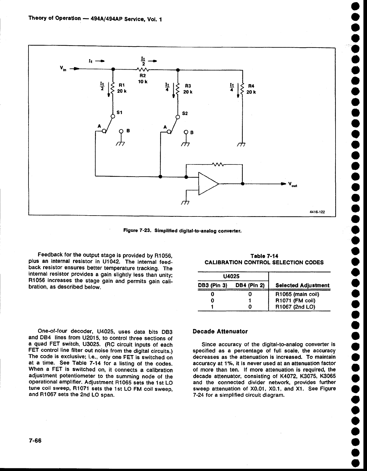
Theory ol Operaton - 4g4A/494Ap
Service,
Vot.
1
R2
Rl 1ok t, I
20k . I
s1
4114122
Flgure 7-23. Simplified digital-to-analog convertGr,
o
o
o
o
I
a
o
o
o
o
o
o
o
o
o
)
a
o
I
t
o
o
o
a
o
o
o
o
I
I
o
o
o
o
o
o
o
o
a
o
o
o
o
o
Feedback for the output
stage
is provided
by R1056,
plus an internal resistor
in U1042. The internal
feed-
back resistor
ensures
better
temperature
tracking. The
internal
resistor
provides
a gain
slightly
less
than
unity;
R1056 increases
the stage
gain
and permits
gain
caii-
bration,
as described
below.
One-of-four
decoder, U4025,
uses data bits DBg
and DB4 lines from
U2015,
to control
three sections
of
a quad FET switch,
U3025. (RC
circuit
inputs
of each
FET control line
filter
out noise
from
the
digital
circuits.)
The
code
is exclusive;
i.e.,
only
one FET
is switched
on
at a time. See Table 7-14 lor a listing
of the codes.
When
a FET is switched
on, it connects
a calibration
adjustment
potentiometer
to the summing
node of the
operational amplifier.
Adiustment
Rl065 sets
the 1st LO
tune
coil
swE€p,
R1071
sets
th€
1st
LO
FM coil
sw€€p,
and
R't
067
sets
the 2nd
LO span.
Table 7-14
CALIBRATION CONTROL
SELECTION CODES
Decade Attenuator
Since accuracy
of the digital-to-analog
converter is
specified
as a p€rcentage
of full scale,
the accuracy
decreases as the attenuation is increased.
To maintain
accuracy at'l./o, it is never
used
at an att€nuation
factor
of more than ten. lf more attenuation is required, the
decade
attenuator. consisting ol K4072, K3075,
K3065
and the connected divider network,
provides
further
swe€p
attenuation
of X0.01
, X0.1,
and Xl . See
Figure
7-24
tor a simplified circuit
diagram.
R1065
(main
coil)
Rl071
(FM
coil)
R1067
(2nd
LO)
7-66
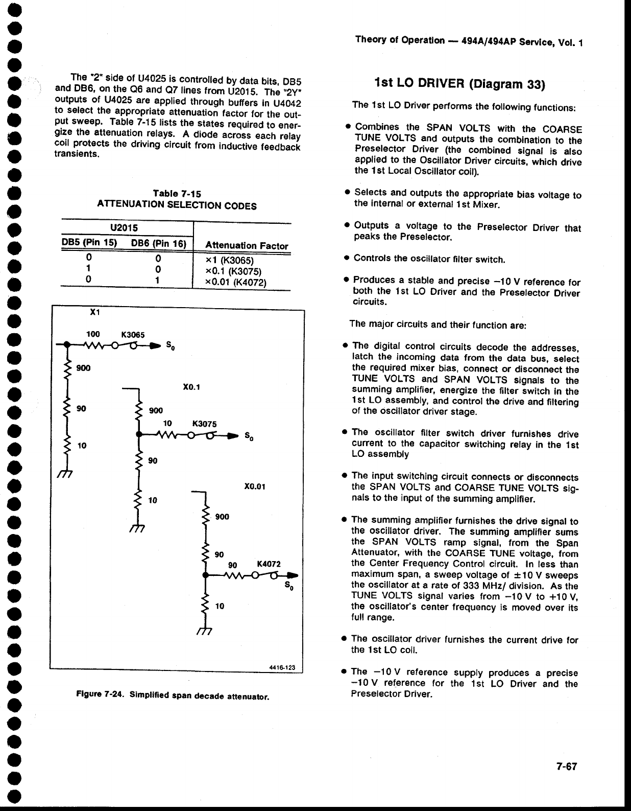
o
O
I
o
o
o
o
o
o
a
a
a
o
o
t
a
o
I
a
a
I
o
o
a
a
o
o
a
a
a
t
I
o
a
o
o
O
o
o
o
o
o
o
I
The
2" side
of U4025
is
contro[ed
by
data
bits,
DBS
and
DB6,
on
the
e6 and
e7lines trom
deotS. The
,,2y,
outputs of U4025
are applied
through buffers
in u4042
to select
the appropriate
attenuation
factor
for the out-
put
sweep. Table
7-1S
lists
the stat€s
required
to sner_
gize
the attenuation
relays. A diode
across
each
relay
coil
protects
the ddung circuit
from inductive
feedback
transients.
Tabte
7-15
ATTENUATION
SELECTION
CODES
Theory of Operation
- 494Al4g4Ap
Servtce,
Vot.
1
1st LO DRTVER
(Diagram
33)
The
1st
LO Driver performs
the following
functions:
o combines the spAN voLTs with the coARSE
TUNE
VOLTS
and outputs
the combination
to the
Preselector
Driver (the combined
signal is also
applied
to the Oscillator
Driver
circuits,
which
drive
the 1st Local
Osciilator
coit).
. Selects
and outputs
the
appropriate
bias voltage
to
the
internal
or
external
1st
Mixer.
o Outputs
a voltage
to the preselector
Driver
that
peaks
the Preselector.
o Controls
the
oscillator
lilter
switch.
o Produces
a stabte
and
precise
-10 V reference
for
both the 1st LO Driver
and the preselector
Driver
circuits.
The
major
circuits
and
their function
are:
o The digilal
control
circuits
decode
the addresses,
latch
the incoming
data from th€ data bus, select
the required
mixer
bias,
connect
or disconnect
the
TUNE VOLTS and SPAN VOLTS
signats
to the
summing
amplifier,
energize
the filter switch
in the
l st LO assembly,
and control
the drive
and
filtering
of the
oscillator
driver stage.
o The oscillator
filter switch driver furnishes
drive
current
to the capacitor
switching
relay
in the 1st
LO assembly
o The input
switching
circuit
connects
or disconnocts
the SPAN
voLTS and
COARSE
TUNE
VOLTS
sig_
nals
to the input
of the summing
amplifier.
. The
summing
amplifier
furnishes
the drive signal
to
the oscillator
driver. The summing
amptifier
sums
the SPAN VOLTS ramp signal, from the Span
Attenuator,
with the coARSE TUNE voltage,
from
the Center Frequency
Control circuit. In less
than
maximum
span,
a sweep
voltage
of *10V sweeps
the
oscillator
at a rate
of 333 MHz/
division. As the
TUNE
VOLTS
signal
varies
from
-10V to +10V,
the oscillator's
center
frequency
is moved
over its
full range.
o The oscillator
driver
furnishes
the current
drive
for
the
1st
LO
coil.
o The -1 0 V reference
supply produces
a precise
-10V re[erence
for the 1st LO Driver and the
Preselector
Driver.
xl (K3065)
x0.1
(K3075)
x0.01
(K4072)
x1
100 K3065
441&r23
x0.01
Flgwe 7
-2,4. Simplifi ed span decade attenuator.
7-67
Theory
of Operafon - 494ful4g4Ap
Servtce,
Vot.
1
r The mixer bias circuit produces
and outputs
the
required
bias voltages
for the 1st
Mixer.
. The programmable
bias circuit provides
peaking
voltage for the
Preselector
or external
mixers
bias
voltage
based on data supplied
by the microcom-
puter.
Digital Control
The
digitat control
circuit
controls
the
osciilator
span
volts, the 1st Mixer bias, and programmabte
bias.
Decoder U4034 output 1 (pin 14) goes low when
the
input address is 72 and output
Z {gin
T) goes
tow for
address 7E. When
output
1 goes
high,
data is clocked
or latched into U4017,
and when output
7 goes high
data
is latched
into
U4024
or tJ4022,
depending
on the
status of data
bits DB6
and
DB7.
Data
for U4017 eonsists
of control
codes for the
oscillator drive circuits and the switches in U1016,
which select
l st Mixer
bias or the
bias set
by
the
front-
panel MANUAL PEAKING
control. The codes are
described in Table
7-16.
Oata at address 7E tor U4022 and U4024 drives
DAC
U3022
and
is converted
to an
analog
signal
which
provides
the
Programmable
Bias.
Input Switching
lf the main coil of the oscillator
is not
to be swept,
DBO
goes
low at address
72. This
cuts off e3029,
de-
energizes K3034,
and disconnects
the SPAN VOLTS
signal to the summing
amptitier. Diode
CR303t pro-
tects 03028 from the inductive
leedback
surges
that
occur at turn-off.
7-68
Oscillator Filter Switch Driver
When
DBO
is low,
relay K3034
is de-energized and
02029 is biased
on which
drives a capacitor
switching
relay on
the 1st
LO Interface
board. The
capacitors
are
switched
acroEs the main coil, when it is not being
swept,
to lilter
noise riding
on
the tuning current.
capa-
citor C2025
provides
a gradual
decay
of current
through
the r€lay
aft€r power
is turned off.
Summing Amplifler
Amplifier U2032 and the compl€mentary
pair of
translstors, 02035 and 02039, plus related com-
ponents, comprise an operational amplifier. The
COURSE
TUNE VOLTS ANd
thE SPAN VOLTS ArE
summed
at the input
to u2032. The feedback
resistor,
for the
operational amplifier, is Rl038. The input
resis-
tance
is R2O27
for the COARSE TUNE VOLTS signal
and R20{}1
for the SPAN VOLTS signals.
(R2030
is
switched across R2031
, as mentioned
previously,
to
increase stage
gain
for maximum span operation.) The
output of the summing amplifier,
which can swing
from
-10 V to +10
V, is applied
to the Preselector
Driver
cir-
cuits and
to the
Video Processor
board.
Oscillator Driver
The output
of the summing
amplifier also
drives
the
input
to the oscillator driver
stage
when FET Q2040
is
switched on. The oscillator
drivEr stage consists
of
active components Q2045,
U2043, Q3047,
and Q352.
The input resistance
consists
of R2041, the
1st
LO
Sen-
sitivity adjustment
R1031,
plus R2043. The feedback
resistance is R2042.
The arnplifier
bonverts a voltage input into a cunent
drive
for the l st LO
tuning
coil
by
controlling
th€
voltage
across current
sens€ resistor R1040, which is in s€ries
with the oscillator tune
coil. 03047 assures that Q352
base
current remains within the
oscillator
tuning
coil
cir-
cuit. Q2040
is biased
on except when
the oscillator
is
degaussed.
The summing
amplifier
output is applied
through the 1st LO Sensitivity
adjustment R1031
and
summed with an offset
voltage set by the 1st LO Offset
adjustment R1032
at the input
to the preamplifier stage
02045. Adjustments
Rl031 and Rl032 match
the
oscil-
lator driver stage to the oscillator characteristics,
R1032 adds offset to the input of the preamplifier
to
place
the oscillator
at center operating frequency
when
the
amplifier
input
is at 0
V.
02045
is a low-noise, matched, dual transistor.
The
feedback
path
through
R3040 and R2042
sets
the vol-
tage across a four-terminal resistor R1040. This
vol-
tage
sets
the current through
the resistor which
is also
emitter current for driver transistor Q352. The 1st LO
Sensitivity
adjustment
Fll031, sets the voltage
gain of
o
a
o
o
a
o
o
o
o
o
I
o
o
o
a
a
o
a
I
o
a
o
o
o
o
o
o
o
o
o
o
a
I
o
t
o
o
o
o
o
o
O
o
O
lnput
iiqnal
Table 7-16
U4017
OUTPUT
LINES
State
DBO
DB1
DB2
DB3
DB4
DB5
DB6
DB7
Bias
1 off
Bias
2 off
Bias
3 off
MANUAL
PEAK off
Not
Used
Driver
input off
Span
Volts
line on,
oscillator
filt€r off
Not
Used
Bias 1
on
Bias
2
on
Bias
3 on
MANUAL
PEAK
on
Not
Used
Driver
input
on
Span Volts
line
off,
oscillator
filter
on
Not
Used
a
o
a
o
I
I
o
o
O
o
I
o
o
o
o
a
a
o
o
o
t
t
o
a
a
o
I
o
a
a
o
o
I
o
o
I
a
o
o
o
a
a
I
o
the amplifier.
This
in turn,
changes
the current
drive
to
the oscillator
coil.
Reference Supply
- .,
Preamplifier
e2052 plus
amptifie
r lJ20S2
and
emitter
follower
Q2051
, are
the
active
compon€nts
of th€
_1
O V
I-ej9fl"":.uppty. Bias for one sid'E
of 02052 is set by
VR1055.
The
other
side.is
set
by
the
_10
V
Adj
R1Og4.
Any change
in the suppty
is amiltiRed
by e20S2
wnicn
changes
the drive
to the pass
transistoi
eZOSt
*nicf,
compensates
for the change. The diode network
across the bas€-emitter junction limits the emitter
current
to about
30
mA, protecting
the transistor
from
damage.
Mixer Bias
Driver
The
mixer
bias
driver
circuit,
which
consists
of quad
IET switch U1016, amptifier
Ul025A, and buffer
O202VA1A28,
plus associated
circuitry,
furnishes
the
required
bias
current (up
to 20
mA)
to ttre t st Mixer
cir-
cuit. The
bias voltage
varies
from
+1 V to _1 V for the
internal
mixer,
and
from
+1 V to -2.25 V
for an
external
mixer. External mixer bias voltage range can be
changed
to -1 to +2.25V by moving
the strap
J2014
from
+12
V
to
the
-12V suppty.
Mixer
bias
is selected,
by the
data
out
of U4017
to
the quad FET switch U1016,
and fed to the inverting
input
of u1025A. The
output
of u1025A
drives
the
base
9f^ 1_Rair of complementary
transistors
e102g and
Q2025
which
provide
the 1st
-ti4ixer
Bias
voltage.
When
any of the D0 to D3 lines from u4017
go tow, the
respective
switch within U1016
closes anld
connects
olg.9!11" Bias
adjustment
potentiometers
or the
output
pj.
^U:_0-18
(the programmabte
bias
tine)
to the input
of
u1025A.
When
the D3 output
of U4017 goes low, U1016
selects
the Programmable
Bias line
ls the 1st Mixer
Bias
source.
This
occurs
when
External
Mixer
mode
is
gelectgd.
The programmable
Bias is set by the data
loaded
into
DAC
U9022
!y the
microcomputei
or by
the
front panel MANUAL pEAK controt. The MAhiUAL
PEAK
control
is connect€d
to the
input
of U201g
when
the DB4
and
DB7
inputs
to U4OZ4 go low
at address
7E
and
turn
Q3019 on. When
MANUAL
pEAK
is setected,
the DAC
output
is set
for O V.
Programmable
Bias
When the microcomputer
sends address 7E to
decoder
U4034,
pin
7 (output
7) goes
low. At the end
of
deta: output
cycle,
data
is clocked
into
either
1J4024
or
Ua032,
depending
on which
latch
is enabled
by DB6
or
DB7. This
data is then
converted
to an analog
current
Theory
of Operatlon
- 4g4Al4g4Ap
Servlce,
Vol. 1
by U3022
which is thE current
sourc€
for operational
amplifier
U2018.
The
resistance
between
outprrt
termi-
nals 16,
2, and 15 of U3022
is th€ input
resistance
for
operationat
amptifier
U2019. R2022
is the feedback
resistance.
The
output
of U20lg is a bias
voltage
that
is fed, via the Programmable
Bias line,
to either
the
Presel€ctor
Driver
board
where it is summed
with
the
drive voltage for the preselector; or, it is fed through
U1016/U1025A,
and e1028/e2025
to the 829Mfr2
Diplexer,
then through
the Transfer
Switch
on the RF
deck
to the External
Mixer port.
PRESELECTOR
DRIVER
(Diagram
34)
The Preselector provides RF input selectivity
between 7.7 and 21 GHz. This selectivity reducei
spurious responses
over this frequency
range. The
Preselector
Driver supplies
the drive iurrent to the
Pr€selector
coil (shown
on Diagram
12) to tun6 the
Preselector.
lt also
furnishes
a voltage
that is propor_
t]o_B! t9 frequency change through the rear-panel
ACCESSORIES
connector
for an external
preselecior,
if
used. The circuit also operates
the filter select
relay
that selects
either
the pr€selector
or Low-pass
Filtei.
The
major circuits
and
their
functions
are:
. The digital control circuit, which stores and
decodes
the data
from the microcomputer
and
con-
trols
the
other
circuits
within
the
preselector
Driver.
The
digitat
controt
circuit
appties
the
spAN voLTS
signal
to the oscillator
voltage
processor
when
FM
coil spans are selected,
selects
the gain of the
oscillator
voltage
processor,
turns off
the
drive
sig_
nal
to lhe
curr€nt
driver
for degauss cycles
or
when
the preselector
is not in use, selects
the lF offset
voltages to be combined with the FINE TUNE
VOLTS
signaf,
adds
noise
filtering
at the
driver
out-
put when
th€ preselector
is not being swept,
and
controls
the filter select
switch.
r The oscillator
voltage processor,
which
attgnuates
and offsets
the input
signal
for application
to the
summing
amplifi€r.
o The lF offset
stage,
which
applies
an
offset
voltage
to the summing
amplifier.
.This offset
is propor-
tional
to the 1st lF frequency
in use, including
the
effects
of fine
tuning
frequency
changes
of the 2nd
Local
Oscillator.
e The summing amplifier. which combines the
effective
oscillator
frequency
voltage
and the lF
Offset
voltage
to drive
the tracking
adjustment cir-
cu,ts.
7-69
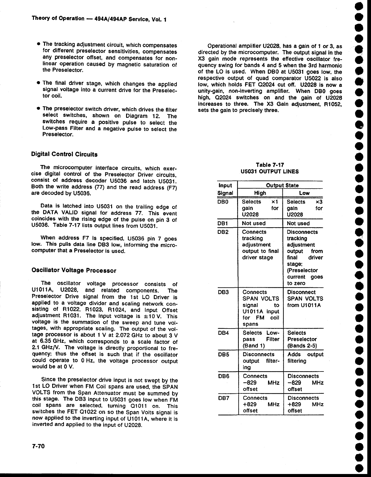
Theory
of Operaton - 4g4A/4g4Ap
Servtce,
Vol. 1
o The
tracking
adjustment
circuit,
which
compensates
for different
preselector
sensitivities,
compensat€s
any pres€lector
offset,
and compensates
for non-
linear operation
caused
by magnetic
saturation
of
the Preselector.
r The final driver stage,
which changes
the applied
signal
voltage
into
a current
drive for the
preselec-
tor coil.
e The
preselector
switch
driver,
which
drives
the filter
sElect switch€s, shown on Diagram 12. The
switches require a positive putse to select the
Low-pass
Filter
and a n€gativg
pulse
to select
the
PresElector.
Digital Control Circuits
The microcomputer
interface
circuits,
which exer-
cis€ digital control
of the preselector
Driver
circuits,
consist of address
decoder US0g6 and latch U5O3l.
Both the write address
(27)
and the read address (F7)
are decoded
by
U5036.
Data is latched
into u5031 on the trailing
edge of
the DATA VALID signal for address 77. This event
coincides
with the rising
edge
of th€ pulse
on pin
3 of
U5036.
Table
7-17
tists
output
tines
from
U5Og1.
When address
F7 is specified,
US0g6
pin 7 goes
low. This pulls
data line
DB3 low,
informing
the micro-
computer
that a Preselector
is used.
Oscillator Voltage Processor
The oscillator voltage processor consists of
Ul011A, U2028, and retated components. The
Preselector
Drive signal from the 1st LO Driver is
applied
to a voltage
divider and scaling
network
con-
sisting of Rl022, Rl023. R1024,
and lnput Offset
adjustment
R1031.
The input
vottage
is *10V. This
voltage is the summation
of the sweep and tune vol-
tages,
with appropriate
scaling. The output
of the vol-
tage processor
is about 1 V at 2.A72
GHz to about g V
at 6-35
GHz, which corresponds
to a scale factor of
2.1 GHz/V. The voltage
is directly
proportional
to fre-
quency;
thus the offset is such that if the oscillator
could operate to 0 Hz, the voltage
processor
output
would
be
at 0 V.
Since the
preselector
drive
input
is not
swept
by the
1st LO Driver
when
FM Coil spans
are
used,
tfre
SpnN
VOLTS from the Span
Attenuator
must be summed
by
this
stage. The
DB3
input
to u5031
goes
low
when
FM
coil spans are selected,
turning 0101 1 on. This
switches the FET
01022
on so
the
Span
Volts
signal is
now
applied
to the inverting
input
of
U1011A, where it is
inverted and applied
to the
input
ol lJ21Zg.
7,70
Operational
amplifier
U2028,
has
a gain
of 1
or
3, as
directed by
the
microcomputer.
The output
signal in
the
X3 gain mode represents the effective
oscillator fre-
quency
swing
for bands
4 and
5 when
the 3rd harmonic
of the LO is used. When
DBo at U5031
goes
tow,
the
respective output of quad comparator
u5022 is also
low, which holds FET c.2024 cut ofi. V2028 is now a
unity-gain, non-inverting amplifier. When DBO goes
high, O2024 switches on and the gain of U2028
increases
to three. The X3 Gain adjustment,
R1052,
sets
the
gain
to precisely
three.
Table 7-17
U5031 OUTPUT LINES
o
O
o
o
e
o
o
I
o
o
I
e
o
o
o
a
o
a
o
a
o
a
o
o
o
o
o
a
o
O
I
I
o
o
o
o
a
o
o
o
o
o
I
o
Input
liqnal High Low
DBO Selects x1
gain for
u2028
Selects
gain
u2028
x3
for
DB1 Not used Not
used
DB2 Gonnects
tracking
adjustment
output to final
driver
stage
Disconnects
tracking
adjustment
output from
final driver
stage;
(Preselector
currerit goes
to zero
DB3 Connects
SPAN
VOLTS
signal to
Ul011A
input
for FM coil
spans
Disconnect
SPAN
VOLTS
from
Ul011A
D84 Selects
pass
(Band
1)
Low-
Filter Selects
Preselector
(Bands
2-5)
DB5 Disconnects
output filter-
ing
Adds output
filtering
DB6 Connects
-829 MHz
off set
Disconnects
-829 MHz
offset
DB7 Connects
+829 MHz
offset
Disconnects
+829 MHz
offset
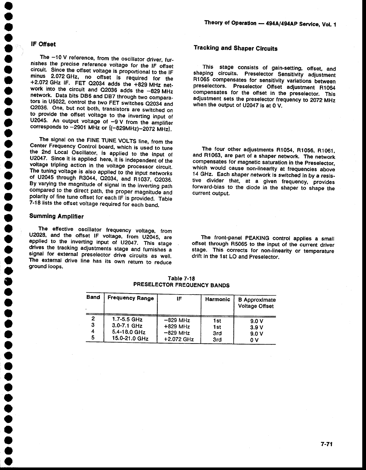
I
o
I
o
a
o
o
o
o
o
o
,
o
o
o
I
o
o
o
I
t
o
e
o
o
O
I
o
a
a
I
I
o
a
I
I
I
o
o
o
a
I
a
o
lF Ofiset
The
-10 V reference,
from the oscillator
driver,
fur_
nishes the precise reference
vo,tage for the lF offset
circuit. Since
the
offset
voltage
is pioportionat
to the lF
mings 2.072
GHz, no ottset id requireo for the
+2.072
GHz tF. FET 02094 adds th€ *829 MHz net-
work into the circuit and e2036 adds the _829
MHz
nehi/ork.
Data
bits DB6
and
DB7
through
two compara-
tors in U5022,
control the two FET
swirches
e203i and
02036. One,
but not both,
transistorb
are
switched
on
to provide
the offset voltage
to the inverting
input
of
U2045. An output voltage
of _-9
V from the amplifier
corresponds
to -2901 MHz
or (_0esnHzy_zot2MHzl.
_ The
signat
on the FINE
TUNE
VOLTS
tine,
from
the
Center
Frequency
Control
board,
which
is used
to tune
the 2nd Locat Oscillator,
is appli€d
to the input of
U2O47.
Since
it is apptied
here,-ii
is independent
of the
voltage
tripling
action in the voltage processor
circuit.
T!:.lulilg voltage
is atso
applied
to the
input
networks
of U2045
through
R9044,
O2Og4,
and R1037,
02096.
By varying
the
magnitude
of signal
in the inverting
path
compared
to the direct
path,
the
proper
magnitudl
and
polarity
of fine
tune offset
for each
lF is provided.
Table
7-18
lists
the offset
voltage
required
for Lach
band.
Summing Amplifier
The effective oscillator frequency voltage, from
U2028, and the offset tF voltage, tiom U2b+5, are
appfied
to the inverting
input of U2C/T. This stage
drives
the tracking
adjustments
stage
and furnishes
a
signal
for external preselector
drivl circuits as well.
The external
drive line has its own r€turn
to reduce
ground
loops.
Theory of Opera0on
- 4g4\l4g4Ap Servlce,
Vot.
I
Tracking and Shaper Circuits
This stage consists of gain-setting,
offset, and
shaping circuits. preselector
Sensitiviiy
adjustment
R1065
compensates
for sensitivity
variations
betwe€n
preselectors. Preselector
Offset adjustment
R10O4
compensates
for the offsst in the presel€ctor.
This
adjustment
sets
th€
preselector
frequency
to 2OTZMHz
when
the output
ot LJaO4T
is at O V.
The four oth€r
adiustments
R1054,
R1056,
R1061,
and Rl 063, are part of a shaper
network. The network
compensates
for magnetic
saturation
in
the
pr€selEctor,
which would cause
non-linearity
at frequencies
above
.1.4
GHz. Each shaper
network
is switched
in by a resis-
tive divider that, at a given frequency, provides
forward-bias
to the diode in the shap€r
to shape
tne
current
output.
The front-panel
pEAKING
control
applies
a small
offset through R5065
to the input of the current driver
stage. This corrects
for nonjinearity
or temperature
drift
in
the l st LO
and
preselector.
Tabte
T-18
PRESELECTOR
FREOUENCY
BANDS
Band Frequency
Range IF Harmonlc B Approximate
Voltage
Offset
2
3
4
5
1.7-5.5
GHz
3.0-7.1
GHz
5.4-18.0
GHz
15.0-21.0
GHz
-829 MHz
+829
MHz
-829 MHz
+2.472
GHz
1st
1st
3rd
3rd
9.0
v
3.9 V
9.0
v
0v
7-71
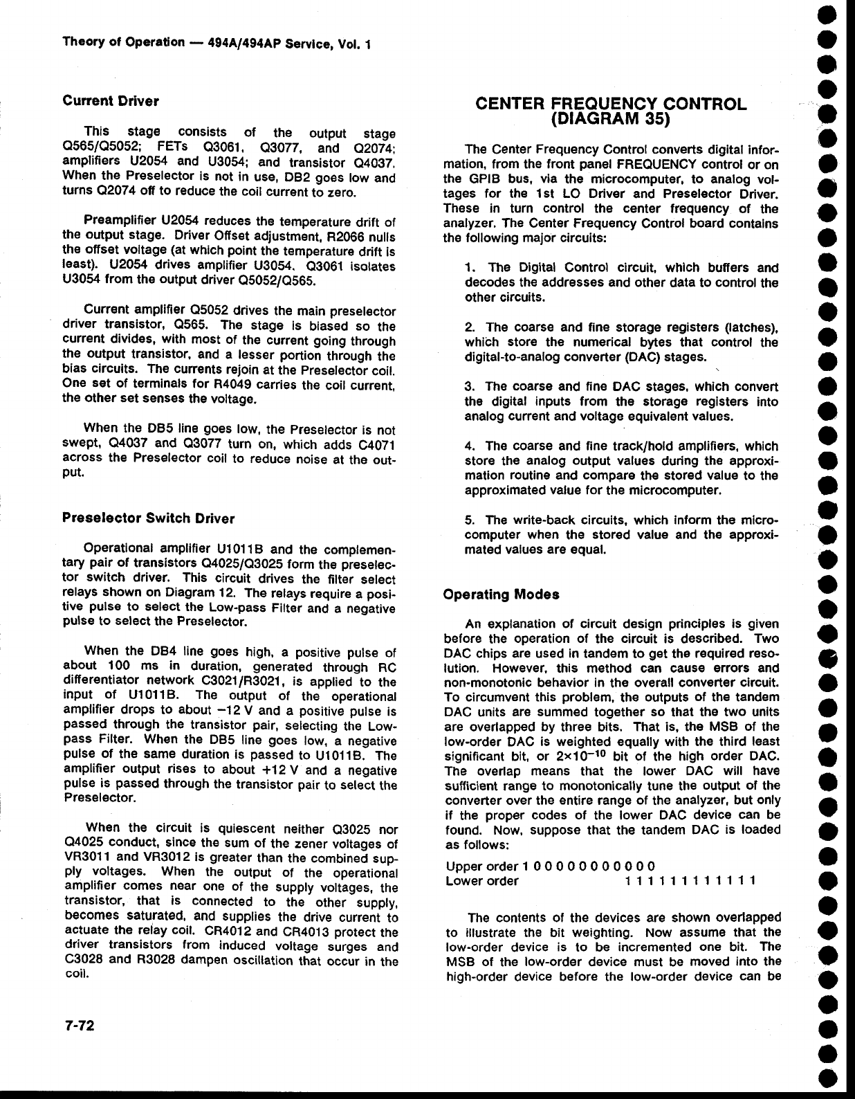
Theory of Operation
- 494A/494Ap
Servlce, Vol.
1
Current Driver
This stag€ consists of the output stage
0565/05052; FETs Q3061, eg077, and e2074:
amplifiers
U205,4 and U3054;
and transistor
e4097.
When
the Preselector
is not
in use,
DB2
goes
low and
turns Q2074 ofi to reduce
the coil current
to zero.
Preamplifier
U2054
reduces
the temperature
drift of
the output
stage. Driver
Ofiset adjustment,
R2066 nuils
the
offset
voltage
(at
which
point
the
temperature
drift is
feast). U2054 drives amptifier
U9054. A9061 isotates
U3054 from the output
driver
Q5052/O565.
Gurrent amplifier
Q5052
drives
the main
preselector
driver transistor,
Q565. The stage ls biased so the
current
divides,
with most
of the current
going
through
the output
transistor. and a lesser
portion
through
the
bias
circuits. Th€ curr€nts
rejoin
at
the
preselector
coil.
One set of terminals tor R4049
carries
the coit
current.
the other
set senses
the voltage.
When
th€ DB5 line
goes
low,
the preselector
is not
swept, Q4037 and Q3077
turn on, which
adds
C4071
across
the Preselector
coil
to reduce
noise
at the out-
put.
Preselector Switch Driver
Operational
amplifier
U10118
and
the complemen-
tary pair of transistors
Q4025/4302S
form th€ preselec-
tor switch driver. This circuit drives the filter select
relays shown
on Diagram
12. The
relays
require
a posi-
tive pulse
to select
the Low-pass
Filter
and
a negative
pulse
to select
the
Preselector.
When
the DB4 line goes high, a positive pulse
of
about 100 ms in duration, generat€d
through RC
differ€ntiator
network
C3021/R302'1,
is apptied
to the
input of ul0118. The output of the operational
amplifier
drops
to about
-12 V and a positive
pulse
is
passed
through
the transistor
pair,
selecting
the Low-
pass Filter. When
the DB5 line goes low, a negative
pulse
of the same
duration
is passed
to U10118. The
amplifier
output ris6s to about
*12 V and a negative
pulse
is passed
through
the transistor
pair
to select
the
Preselector.
When the circuit is quiescent
neither
e3025 nor
04025 conduct,
since
the sum
of the zener
voltages ot
VR3011
and
VR3012
is greater
than
the combined
sup-
ply voltages. When the output of the operational
amplifier
comes near one of the supply
voltages,
the
transistor, that is connected
to the other supply,
becomes
saturat€d,
and supplies
the drive current
to
actuate
the reiay coil. CR4012
and
CR4013
protect
the
driver transistors
from induced voltage surges and
C3028 and R3028
dampen
oscillation
that occur in the
coil.
7-72
CENTER FREOUENCY
CONTROL
(DIAGRAM
35)
The Center
Frequency
Control
converts
digital infor-
mation, from the front panel
FREOUENCY
control or on
the GPIB bus, via the microcomput€r,
to analog
vol-
tages for the 1st LO Driver and Preselector
Driver.
These in turn control the center frequency
of the
analyzer.
The Center Frequency
Gontrol
board contains
ths tollowing major circuits:
1. Tha Digital Control circuit, which buffers and
decodes the
addresses
and other
data to control
the
other circuits.
2. The coars€ and fine storage registers (latch€s),
whibh store the numerical bytes that control the
digital-to-analog
converter
(DAC)
stages. .
3. The coarse and fin€ DAC stages, which convert
the digital inputs from the storage registers into
analog curent and voltage
equivalent
values.
4. The coarse
and fine
track/hold
amplifiers, which
stor€
the analog output
values
during th€ approxi-
mation
routine
and compare
the stored
value
to the
approximated value for the microcomputer.
5. The
write-back
circuits.
which
inform
the micro-
computer when the stored value and th€ approxi-
mat€d valu€s
are
equal.
Operating
Modes
An explanation
of circuit
design
principles
is giv€n
before
the operation of the circuit is described. Two
DAC chips are used in
tandem to get
the
required reso-
lution. However, this method can cause errors and
non-monotonic behavior in the overall converter
circuit.
To circumvent this problem,
the outputs
of the tandem
DAC
units
are summed
together
so that the two units
are overlapped
by three bits. That is, the MSB of the
low-order
DAC
is weighted equally with the third least
significant
bit, or 2x10-to bit of the high order DAC.
The overlap means that the lower DAC will have
sufficient
range
to monotonically
tune the output of the
converter over the
entire
range
of the
analyzer, but
only
if the proper
codes of the lower DAC device
can be
found. Now,
suppose
that the tandem
DAC is loaded
as follows:
Upper order
1 0 0 0 0 0 0 0 0 0 0 0
Lower order 111111111111
The contents ol the devices are shown overlapped
to illustrate the bit weighting. Now assum€ that the
low-order device is to be incremented one bit. The
MSB of the low-order device must be moved into the
high-order device before the low-order device can be
t
o
o
O
I
o
o
o
o
o
I
o
o
o
a
a
a
a
o
I
I
o
o
o
o
o
3
o
o
,
o
I
o
o
a
o
a
o
o
o
o
I
o
t
I
o
o
O
a
o
o
t
o
o
I
,
o
o
o
o
a
t
t
o
I
o
a
o
o
O
a
o
a
I
o
I
o
O
t
O
I
o
o
o
o
o
I
o
lf the high-order
device operated
with no overatl
linearity
inaccuracy,
the operation
would now be com-
plet€ and the low-order incrementing
could occur.
However,
th€ DAC
device
can vary byine LSB
of the
correct
value. Figure 7-25 illustrltei a graptr
of the
b€st and worst case output. Not€, that-even
in the
worst case, the output may move onty once every
two
or three state changes,_but
the outpuf
is always
mono_
tonic
and within
one LSB of the correct
value.
incremented.
Thus,
the
two must
appear
as
follows:
Upperorder
1
0
0 00 0
O
O
O 1
0 O
Lower
order 01'l 111111111
Theory
of Operation
- 4g4Ll4g4Ap
Servlce,
Vol. 1
the basic clrcuit. Whil€ the circuit opgrates
in this
mod€,
the
amplifier
tracks
the DAC
stage
and
sends
the
voltage
out
to the
tuning circuits.
When the transfer
of bits from the lowgr to the
upper
DAC ls required,
the microcomputer
commancls
the circuit to shift to the hold mode. Th€ command
comes
through
the decoder
to shut
off the disconnect
stage.
and
the
preamplifier
output
is disconnected
from
the integrator. Th€ integrator holds th€ voltage that
was previously
at the output
for comparison,
and the
approximation
cycle
begins.
The microcomput€r
resets the low-order
DAC to
zero. Then,
th€
highest
order
bit in the low-order
DAC
is set to one,
and th€ circuit
is queried
to find if the
DAC
output
and integrator
output
is
greater
or less
than
required. lf less. the microcomput€r
loads the next
lower
bit in addition
and
queries
the
circuit
once
more.
This
process
goes
on until
the
two
values
are
the same.
Had
th€
microcomputer
found
that
the DAC
output
was
greater
than
the integrator
output
at the
first
inquiry,
it
would
have
set
the
highest
ordEr
bit
to zero and
loaded
the second-order
bit into
the low-order
DAC.
then con-
tinued
to load successively
lower
order
bits,
one at a
time,
until
the circuit
signaled
that
the comparison
had
reversed.
By this
process,
which
is known
as the suc_
cessive approximation method, the circuit finally
reaches
the
point
where
the outputs
are €qual,
and
th6
microcomputer
commands
the circuit
to shift back
to
the
track
mode.
Digital
Control
The digital control
circuits
consist
of buffer U4Og5,
address
decoder
U4045, steering
register
U4025, and
the steering
gates
(U4015A,
U40158,
U401SD,
U4O6OA.
U4060B,
and
U4060D). Because
of the
large amount
of
data that must
pass
through
these
circuits, a steering
register
that
has a separate
address
is used.
The
steering
byte, is clocked
into
U402S
at addr€ss
70. The
outputs
are applied
to the steering
gates,
and
the circuit
waits
for the next
byte.
The microcomputer
then furnishes
the first byte ol
data
to be sent
to the low-order.
fine-tune,
DAC via
the
storage
register.
Latch u3015 and
part
of U3025
form
one storage
register
for the low-order,
fine-tune DAC.
The
byte
is clocked
into
the
register
by the
coincidence
of low states
at the inputs of the steering
gate
(u4015A
or U401
5B);
one from the st€ering
byte
and the other
from ADDRESS
71 signal,
which
is used to clock
the
steered
data bytes into the correct
register.
This con-
tinues
until seven
bytes of data have
b€en
clocked into
the
register.
including
the
steering
byte.
Figure Z-2S. DAC Varlance graph.
ff, In the example
shown
previously,
th€ high-order
device is at point A in Figure
7-25, incrementing
the
device to point B has no effect on the output. lf the
MSB
of the low-order
device
is set
to zero,
as
shown
in
the first example,
the combined
output will actually
de.crease-
Ordinarily,
the
Center
Frequency
Control
cir-
cuit
can
increment
and
decrement
whenever
the micro_
computer
commands
without going through
a special
routine. However,
as just described,
some
microcom-
puter
adjustment
is necessary
to compensate
for the
disparity
that
usually
occurs
between
the
low-order
and
high-order
DAC
units.
The first operating
mode is the tracking mode,
where the preamplifier
and integrator
are connected
together
by the disconnect
stage, and the entire
unit
acts as an operational
amplifier.
Figure
Z_26
illustrates
t-
--;
il WORST-CASE
OUTPUT
-r-]*-
BEST.CASE
OUTPUT
Mr6.124
7.73
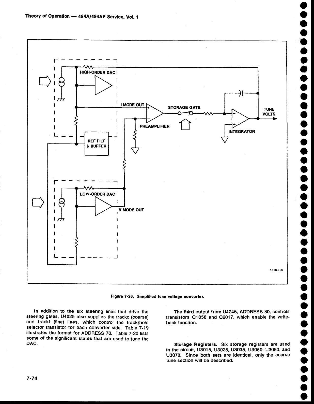
Theory
of Operaton - 494[l4g4Ap Servlce,
Vot. 1
Figure
7-26. Simplilied
tune voltage converler.
a
o
o
o
I
a
t
o
o
a
I
I
o
O
o
o
o
O
a
t
o
o
o
a
o
o
I
o
a
,
o
a
a
o
o
o
o
o
o
o
o
I
a
o
In addition
to ihe six steering lines
that drive the
steering
gates,
U4025 also
supplies
the
trackc
(coarse)
and trackf (fine)
lines, which control the track/hold
selector
transistor for each
converter
side. Tabte 7-1 9
illustrates
the format
for ADDRESS
70. Table
7-20
tists
some
of the
significant
states
that are used
to tune the
DAC.
The third output from U4045,
ADDRESS
80,
controls
transistors 01058 and O2017.
which enable the write-
back function.
Slorage
Reglsters. Six storage
registers
are used
in the
circuit, U3015,
U3025, U3035, U3050,
U3060,
and
U3070. Since both sets are identical, only the coarse
tune
section will be described.
I
I
I
I ruooeour
Dl
PREAiIPLIFIER
INTEGRATOR
V MODE
OUT
'141&126
7-74
I
o
a
o
a
a
o
o
o
O
I
t
o
o
I
o
o
o
a
a
t
o
a
o
a
C
I
o
I
o
o
I
I
e
a
o
I
o
o
o
o
o
a
o
.Data
from U4035,
the data
buffer,
is clocked
into
the
registers
each
time
a difierent
tune
voltage
is required.
U3050
feeds
the
lowest
eight
bits
to thE
liw-order
DAC,
u2055; U3070
teeds
the higlgs1
eight
bits of the high-
order
DAC,
U2060.
Registei
U3060ieeOs
the
remaining
bits of both
units.
Theory
of Operaton - 4g4ful4g4Ap
Servlce,
Vol. 1
Each
side
of the converter
has
two DACS
summed
log€ther
to produce
an output
of approximately
*10 v.
The DACs
ar€ programmable
curreni generatois
driving
the preamplifier-integrator
circuit. ttre higtr-orOer
DAd
provides
0 to 2 mA of current to the circuit
via the
buffer,
while
the low-order
DAC
provides
approximately
+2.5 mV
at the inverting
input
of the
pr€amdifier.
fn6
prearnplifier
then drives the integrator via the storage
gate.
An isolated ground system for each half of the cir-
cuit minimizes
susceptibility
to noise
and €xtraneous
signals. This is because
the convefiers provide
the dc
voltages
that
tune
the oscillators.
Track/Hold Amptifter
. The amplifier
consists
of high_order
DAC U2O6O,
low-order DAC U20S5, buffer U2O5O,
preamptifier
Ul065,
storage
gate
01065.
and
integrator
|J21TA.
. -The
circuit
output
is required
to tung approximately
*10 V for the fuil-scale
range
of U2060.
ialnen
U2060
is off and
the output
of u2050
is at 0 v, the +10
v out-
put level is set by 1 mA of curr€nt
through
R1055,
and
the combination
ot R1092,
R1053,
anct R1070. When
u2060
is fuily
on,
and
output
of u2050 is at +10
v. the
-10 V output
level
is set by 2 mA of current
through
R1052,
less the I mA constanfly
flowing in R10S5.
Full-scale gain
is adjusted
by R1032.
Resistors
RlOS2,
R'|
053, and R1055 are matched for temperature
coefficient
to minimize
output
voltage
drift as a function
of temperature.
DBO
DB1
DB2
D83
DB4
DB5
DB6
DB7
Tabte
7-19
ADDRESS
70
FORMATS
Fine
Tune
low
byte
enable
Fine
Tune
middle
byte
enable
Flne
Tune
high
byte
enable
Fine
Tune
hold
Coarse
Tune
low byts enabfe
Coarse
Tune
middle
byte
enable
Goarse
Tune
high
byte
enable
Coarse
Tune
hold
Dlgital-To-Analog Converters. Since both the
coarse and fine tune circuits operate similarly,
only the
coarse
tune section of the board will be discussed
here.
Figure
7-26 is a functional
block diagram
of the circuit.
Tabte
Z-20
DAC
TUNING
CODES
Polnt
Positive
full
range
Mid-range
Negative
full-range
Results
Enables
all latches,
track
mode
Loads
zeros
into
all
positions
of both DACs
Enables
all
latches,
track
mode
Loads zeros into all positions of both DACs
Enables
high byte latch, track mode
Loads 80 into DACs. Midrange value
Enables
all latches,
track mode
Loads FF into all positions of both DACS
7-75
Theory
of Operalion
- 4g4A/4g4Ap
Service,
Vol. 1
Low-order DAC U2055 tunes approximately
+2.5mV at pin
1. and its gain
is adjusted
by R1O2S.
l!e^ gain
oj p-r_elmplifier
U1065
is set at approximatety
10,000
by Rl056 and
the
5O combination
of R2O59
ana
R2060.
The combination
of CR1056,
CRlO58,
RlO54,
and R1059 limits
th€ gain of U1065 when the output
exceeds
approximately
0.7
V in either
direction.
Write-Back Circuit
This
circuit
consists
of comparator
Ul055 and
ena-
bling transistor Q1058. When
it is necessary
to do a
carry
between the
low-
and
high-order
DACs,
the circuit
is put into the hold
mode
by turning
ofr
Q1065.
U2060
is incremented one
bit and
U2055 is reset to all zeroEs_
The output of u1065 is now at something other
than
0 V. The purpose of th6 following
approximation
rou-
tine is to get output
of U1065 as close
to 0 V as possi-
ble before
switching
the circuit back into
track rnode
by
tuming on Ql065. Comparator
Ul055 det€cts
whether
the output of U1065 is above
or below
coarse
tune
ground. The
instrument
rnicrocomputer
begins to exer-
cise
th€ low-order DAC bits one at a time
from
MSB
to
LSB. After each
bit is turned
on, U1055
ls enabted
by
turning off Q1058. lf U1055 detects
that the output
of
u1065 has crossed
0v, that bit is turned
ofr and
the
next lower
bit is turned
on. This continues
through
all
12 bits and when completed,
th€ output of U1065
should
be close
to 0V. Transistor
Q1065
can
now
be
turned back on without
causing
excessive
jumping
of
the
signal on
the screen.
-10 V Reterence Buffer
The
circuit uses
the
voltage
reference developed on
the 1st LO Driver
board
as a reference for the DACs.
Differential amplifier
U20/5 receives
the -10 V refer-
ence and -1 0 V reference retum, and removes
eny
common-mode signals present. Resistor pairs
Rl048/R1049 and Rl050/R1051
are matched
for tem-
perature
coefficient
to minimize reference voltage
drift
over
temperature.
a
o
I
o
a
o
o
o
o
t
I
o
o
o
o
a
o
o
o
a
o
I
I
o
o
c
o
a
o
t
o
o
t
o
a
o
o
o
o
o
o
o
o
o
U1065
is connected
to integrator
U2OT0
via
storage
gate
Q1065,
which
is on in the track mode. Transistor
01065 is turned off any time a DAC
is being
tuned
to
allow
the DAc output
to settle
before
tuning
the
output
of U2070. lt is also
turned
off during
the interval
when
a carry from the low-order DAC to the high_order
DAC
occurs. Transistor Ql065 is controlled by e1061.
When
Q1061 is on,
CR1064
is reverse-biased-
The
vol-
tage at the gate of e1065, which is developed
by
R1064,
R1065,
R1067,
and R1066,
is near O
V ana
Q1065 conducts. When
e1061 is off, voltage
to pinch
off
Q'l065
is apptied
through
R1062
and
CR.t
064.
v2070
tracks
the
output
of U1065 when
the circuit
is
in the
track mode
and serves
as the inverting
amplifier
in ths fe€dback
system
shown
in Figure
7-26. Normally
the incoming signal is routed through R2067. T;
improve
tl.e slewing
rate
of the integrator,
CRI
067 and
CR1069
conduct and connect R1O6g
across R2067
when
input
signals
over
1 V are
present.
7-76
I
o
a
o
o
a
o
o
o
o
o
)
o
o
o
a
a
I
t
I
I
o
o
t
o
o
I
o
I
o
o
o
o
e
o
o
I
o
o
o
o
a
o
o
Theory
of Operation
- 4g4ful4g4Ap
Service,
Vot.
1
100 MHz reference
signal
from th€ grd Converter,
is
divided
down
to 25
MHz, on
the
Synthesizer
board,
and
applied
as the reference
signal
to the mixer
on the
Offset Mixer
board. The 25
MHz
signal
is also
applied
as a clock signal
to +N counter
circuits,
on the
'Syn-
thesizer
board,
which output
a frequency
(depending
on
the +N number from th€ processor) tieiween g2lHz
and 94 kHz. This signat is apptiect to the
phase/frequency
detector
on the Offset
Mixer board.
where it is compar€d to tho lF output (difierence
between
th€ 25 MHz reference
and the autput
trom the
VCO
(voltage
controlled
oscillator)
and any difierence
is
output
as an
€rror
voltage
to the Enor
Amplifier.
The VCO operates between 25.032
MHz and
25.094
MHz, depending
on th€ driv€ from the Error
Amplifier.
This signal
is apptied
to thg RF input
of the
mixer on th€ Offset
Mixer board,
where
it mixes
with
the 25 MHz reference
frequency. The difference
fre-
quency,
which
is between
32kHz and
94 kHz,
is
applied
t1 thj phase/frequency
detector
and compared
to the
+N frequency. lf the two signals are edge and fre_
qugngy
coincident,
phase
lock occurs. lf they
do not
coincide,
an error
signal
is generated,
passed
through
the Error
Amplifier,
and
apptied
to the VCO
to shift
the
oscillator
frequency
until
it is phase
locked. This
evolu-
tion typically
lasts
for only a few milliseconds,
so the
inner
loop
phase
lock
is essentially
instantaneous.
The_ outer loop,
which includes
the inner loop cir-
cuits (Offset
Mixer,
Error
Amplifier,
and VCO) consists
of the Strobe
Driver,
phase
GatE,
Error
Amplifier,
and
1st LO. (fhe Harmonic
Mixer, Auxiliary
Synthesizer,
and Counter, are a part of the operation,
but are not
considered
a part
of
the
foop.)
The signal between 2S.0gZ
MHz and 25.094
MHz
from
the VCO
is
applied
to the Strobe
Driver where
it is
divided
by five, filtered,
and sent to the phase
Gate
Detector
as a strobe signal
between
5.006
MHz and
5.01
9 MHz. This
strobe generates
line
spectra
that
are
egually
spaced approximately
S
MHz over the spec-
trum. At about
the 400th line, which corresponds
to
2 GHz, assuming
that the l st LO is tuned to a fre-
quency
near 2 GHz, one of these lines (at about
the
400th
line)
will be within
2.5MHz of the 1st LO fre-
quency. The Phase
Gate
Detector will then
output
an
enor signal that is proportional
to the dilference
between
the lst LO frequency
and
that of the nearest
strobe line, if that difference
frequency
is less than
approximately
1 MHz.
For phase-lock
acquisition,
the microcomputer
cal-
culates
the strobe
frequency
required
for the desired
l st LO frequency.
The strobe is set to this lrequency
and the lst LO is set to the required
harmonic of the
strobe. The outer
loop is closed,
and the microcom-
couNTER
and
PHASE
LocK
sEciloN (Diagram
g)
FUNCTIONAL
DESCRI
PTION
This section consists of a Counter,
phase Lock
assembly,
phase Gate,
Harmonic
Mixer,
and Auxiliary
Synthesizer.
The Counter,
Harmonic
Mixer,
and
Auxili-
ary
Synthesizer,
form the
nucleus
of the frequency
con-
trol hardware
for the instrument.
Both
the lst LO and
2nd
LO frequencies
are
controlled
via
a firmware
based
control
loop that uses
data
from the Counter
as feed-
back
to control
oscillator
frequency.
The
10
MHz
lF is
also
counted
to accurately
calculate
signal
frequency.
The
phase
Lock
assembly
stabilizes
the t st LO fre-
guency.
lt consists
of an
outer
and
inner
loop.
_ --l!g- inner loop uses the subharmonic
of the
100
MHz reference
frequency,
from the 3rd Converter,
to mix
with
the output
from
a 2i.Og2to
25.095
VCO
and
compares
this lF difference
with
a +N number
(between
32 kHz 3nd 94 kHz) set by the processor.
Any devia-
tion is detected
by a phase/frequency
detector
whose
output
enor voltage
is used
to pull
the VCO
frequency
and
phase
into
lock
with
the
inner
loop
reference.
_ . The
_outer
toop
consists
of the
inner
loop,
a Strob€
Driver,
Phase
Gate Detector,
Error
Amplifier,
and th€
1st
LO. The
frequency
of the inner
loop
VCO
is divided
down and
applied
as a strobe
putse
to the phase
Gate
Detector.
This
strobe.pulse
contains
energy
at frequen-
cies equally
spaced
throughout
the specirum. One
of
these frequencies
wiil be within
2.5
Mi{z of th€ l st LO
lrequency
at
the other
input
to the
phase
Gate
Detector.
The Phase
Gate Detector
outputs
an error signal
pro-
portional
to the difference
between
the nearest
strobe
and
th€
lst LO
frequency.
This
error
signal
is amplified
and
filtered
by
the Error
Amplifier
and
aiptieO
to the
FM
coil of the 1st LO to pull it into trequency
and phase
lock
with
th€ strobe.
The Harmonic
Mixer mixes the 1st LO freguency
and a harmonic
of a synthesize
d 200-2ZA
MHz
'signal
from
the.
Auxiliary
Synthesizer.
The
exact
frequency
of
the synthesizer
signal is a function
of the +N factor
from the processor. The Harmonic
Mixer output
is a
signal
within
the 10 to g0
MHz range. This signat
is
divided
in the Auxitiary
Synthesizei
and sent to the
Counter. The microcomputer
looks at the resultant
count
and decides
which
way to move
the 1st LO to
bring it to ths
correct
frequency.
Phase
Lock Assembly
. As previously
stated,
the phase
lock system
con_
sists
of two frequency
servo
loops,
called
the outer
loop
and inn€r loop. In the inner loop operation, the
7-77
Theory of Operation
- 4g4A/4g4Ap
Service,
Vol. l
puter tunes the l st LO frequency
through
the following
sequence;
up 750 kHz,
down
i.5 MHz,
up
1.5 MHz,
ani
down
750
kHz.
During
one
of these
yirmware
searches,'
the lst LO frequency
passes
through
the strobe
har-
monic frequency
and
th€
loop
acquires
lock.
Any frequency
difference
between
the strobs
signal
and
the 1st
LO
will
generate
a low frequency
conection
voltage. This correction
voltage is filtered by the F(s)
amplifier,
then
used
to drive
the oscillator
FM
ioilto puti
the oscillator
frequency
back
to the strobe position.
tf
th€ lst LO drifts beyond
the error voltage range
of the
F(s) amplifier,
comparators
on the Error
Amplifier
board,
that monitor the error voltage,
wilt interrupt
the micro-
computer
and
indicate
the
direction
of drlft. The
micro-
computer
then
tunes
th€
center Frequency
control cir-
cuits
to null out any
FM coil current
in thL phase
tock
loop.
Frequency Control
The 21
-bit
counter
and
its associated
control
circui-
try,
on the Counter
board,
plus
the
Harmonic
Mixer
and
Auxiliary Synthesizer,
form the frequency control
hardware nucleus for the spectrum analyzer. A
firmware-based
control loop, that uses data from the
counter
as feedback
on the oscillator
frequency,
con-
trols both
the lst LO and
the
2nd
LO frequenciel.
tne
l0MHz lF is also
counted
by the Counter
to d€termine
the input
signal
frequency
to th€
analyzer.
A mix down
counting
scheme
is used
to count
the
lst LO frequ€ncy,
which varies between
2 GHz and
6 GHz. 'fhe 2O0-220
MHz output from the Auxiliary
Synthesizer
is positioned
so one of the signal harmon-
ics is approximately
45
MHz above the lst LO fre_
quency. This output drives
the LO input to the Har-
monic
Mixer,
the
1st
LO
drives
the
RF
input.
One
of the
lF outputs
from
th€ Harmonic
Mixer is within
the 10
to
80
MHz
range (approximatety
45 MHz). This
tF signal
is
passed
through
a 10-80
MHz band-pass
filt€r,
divided
by 100,
then counted
by the
Counter.
Since
the
proces-
sor knows the Synthesizer
frequency,
the l st LO fre-
quency
can
be calculated
if the processor
knows
which
harmonic
of the Synthesizer
frequency
was used to
generate
th€
lF frequency
being
counted.
The harmonic
of the Synthesizer
frequency
is calculated
from
the 1st
LO tuning
DAC
(digital-to-analog
converter)
code, since
it indicates
the 1st LO frequency
to within approxi-
mately *10 MHz.
Counting
the znd LO frequency
is much simpler.
The controllable
16-20
MHz
VCO
in the 2nd
LO
assem-
bly determines
the frequency
of the 2nd LO;
therefore,
the 2nd LO frequency
is calculated
by direcily counting
the 16-20
MHz signat. The 2nd LO frequenty
is then
calculated
from
this frequency.
Confolling fte O3clllator Frequency. The fre-
quency control loop is only closed between swesps.
After the completion of each sweep, the processor
switches
the span/div
to zero and
then
counts
the lst
LO and the 2nd Lo frequencies.
tf they
ar€ not at the
frequency
required
to generate
the displayed
cEnter
tre-
quency,
they ar6 set to the correcl frequency
by repeat-
ing
the process
(i.e.,
the DACs
are changed
to tune
the
LO,
the LO
is counted,
€tc.).
In the single swsep
mode,
the
oscillator
frequencies
ar€ corrected
after each single-swe€p actuataon.
and
before
th€ sweep
starts. In the manual sweep
mode,
or
other non-rscurring sw€eps, the oscillators ars
corrected
at p€riodic
intervals.
Counting the lF. In addition
to counting
thE fre-
quency
of the
1st and
2nd
LO, the 10 MHz lF is counted
when
the
Counter
mode
is actuated;
thus, the incoming
signal frequency can be calculated
from the frequency
conversion
equation for the analyzer. The 1st LO is
actually
phase
locked before
the 2nd LO and lF are
counted, in
order
to reduce
FMing
in
the
lF signal.
This
allows very accurate signal counting, even in wide
spans.
HARMONIC
MIXER
(Diagram
36)
The Harmonic Mixer combines
a portion
of the 2-
6 GHz 1st LO signal with harmonics of the 200-
220 MHz refersnce
signal
from
the
Auxiliary
Synthesizer
to provide
an output signal in the 10-80 MHz range.
This signal is amplified
and returned
to the Auxiliary
Synthesizer where
it is counted
to get
an
exact compu-
tation of the oscillator
frequency.
The Harmonic Mixer
consists
of a directional
coupler, an input
amplifier,
the
mixer, and an output amplifier.
all on a hybrid circuit.
Figure
7-27 is a functional
block diagram
of the Har-
monic
Mixer.
Input signal level, from the lst LO to dirgctional
coupler
A2541,
is a about +10 dBm. The
coupling ratio
is 1O
dB, th€refore, the coupler
will delaver
about l mW
(0
dBm) to the RF input of the harmonic
mixer. The
through-port
contributes about
0.5
dB of loss for the
2-
6
GHz
signal.
The 200-220 MHz reference signal, at a level of
about 10 mW from the Auxiliary Synthesizer, is
amplified
to a level of about
100 mW (+20dBm) by a
difier€ntial amplitier Ql and
Q2. Resistor R27 couples
the emitters together and
the
current
is set by R13 and
Rl4. Output
is transformer coupled
to the input of the
mixer. Input signal level to the amplifier
is +7 dBm
minimum.
7-78

I
t
a
o
o
a
a
t
o
o
o
t
I
o
o
o
a
o
o
I
o
o
o
o
o
o
o
o
o
t
a
o
I
o
a
I
t
I
t
o
I
o
a
o
Theory
of OperaUon
- 494Al4g4Ap
Servtce,
Vot.
1
Output
Amplifier
LO AIIPLIFIER
4416-200
Flgute 7-27. Slmplified schematic of harmoolc mixer.
Two
additional
directional
couplers
are
used
to cou-
?f..lh" 1-9c!. signat
into
the
mixer
circuit.
A power
ll,ll"l,lll .12,
Rsl sptits
the sisnar
into
two paths.
FFcn
stgnat
(approximately
_6 dBm each)
is then
cou_
pled through
these
coupleis to ttre mixer. Tfre
ttrroujtr
ports
are
terminated
in 50 ohms. Thus
the
2-6
GHz
iig-
nal is coupted
into the mixer Oinerentiatty
at a power
level
of
about
-16 dBm.
The 200-220
MHz reference
signal
is also coupled
differentially
into the mixer circuit,
since
the output
ot
::11^.j:jlT,
r1_
is:pptied across
*," uJ terminatins
restsrors
R4 and R5. The level
of this signal
is higi
enough
to drive
the snap_off
diode
into its-
operational
region. Harmonics
of this 2@-Z2O
Mnz silna mix
with
th.e.
?-6
GHz signal
to generate
numerouJ
lF products
:vhich.ar:
detected
by diodes
CR2
and
CR3
ano
fed
to
rne
output
amplifier.
The
output
amplifier
is a two stage
common-emitter
cascade
amplifier
with dc couplinj between
stages.
The standing
curr€nt
through
ttre
sjconO
stage
(e4) is
higher
than in the first stlge (a3) to provide
better
power
and intermodulation
performance.
Th€
amplifier
is designed
for a 10 to gO
nl|Hz
response. Signals
above
80Jr4Hz
are rejected
by a tow-pass
filter
in the
Auxillary
synthesizer.
Output
level
of signals
in
the
10_
99 Yt-rltg.e is
typicalty
-20
dBm
ror
inpri
sisnat
tev-
els as
described.
AUXILIARY
SYNTHES|ZER
(Diagram
37)
The Auxiliary
Synthesizer
is part of the spectrum
analyzeis Direct Frequency
Readout (DFR)
systern.
This,
along
with
a harmonic
mixer,
counter
circuiti,
sup-
porting
filters
and
amplifiers,
and
appropriate
firmware,
make
up the DFR. The DFR provides
th€ ,neans
tor
measuring
and determining
the frequency
of all
oscilta-
tors and
the center
of the lF, so the cenier
screen
fre-
quency
is always known.
Since
the lF signal
can be
counted,
this allows
direct frequency
measurement
of
any signal applied
to the input port of thE spectrum
analyzer.
A functional
block
diagram
of a simple
or basic syn-
thesizer
is shown
in Figure
7-2g. The
VCO frequency
is
divided
by "N"
in a programmable
down-counter
which
outputs
a-pulse
every
Nth input putse. This
frequency
along with a frequency
reference
is then fed-
to i
phase/frequency
detector. The difference
between
the
two signals
is filtered
and
fed back
as a control
voltage
to the
VCO
to phase
lock
the oscillator
to the r€ference.
VCO frequency is related to the reference by,
Fret
- NFrer_
As N is changed,
the VCO
trequency
will
change
by Frer
for each
step in N. This produces
out_
puts
separated
by Fr"r.
To get
closely
spaced
channels,
in tuning the VCO,
the reference
frequency
must be
relatively
low.
7-79

Theory of Operation
- 4g4A/494Ap
Service,
Vol. 1
PHASE/FREO
DETECTOR
fr:t,orF:NF,
Figure
7-28. Block diagram
of a baslc syntheelzer.
Phase/Freq
DETECTOR
mOD
CONTROL
F,n : (NP + A) Frct
o
a
t
o
I
o
o
o
o
o
t
o
o
o
o
o
o
o
o
I
o
o
o
a
o
o
o
o
o
a
C
a
o
a
o
I
o
a
o
O
o
a
o
O
Figure 7-29. Basic block diagram of a +N syntheeizer with a variable modulue prescaler.
This
synthesizer
uses
a variable
modulus
prescater
to divide
the
VCO
frequency
before
is processeO
by
the
"+N"
counter,
such
as shown
in Figure
7-29. The
vari_
able.
modulus
prescaler
is iontroilej by
a moclulus
con_
trol input. When
the
line
is high
tne
pr6scater
is
a divide
by P+l and
when
the
tine
is l6w
the
division
cnange"
to
P. A common
type of.
pre.scaler
is a *1g1li. A cy:crc
of
system
op€ration
starts
with
all programmable
counters
loqOe!.1n9
*OV to count. The'var]able
modutus pres-
caler
initiaily
divides
by
p+1.
Two programmable
dividers
are
used
with
this sys-
te-T,
qoth
triggered
by the prescaler
output. One
is a
+N, yith N being
a relatively
large
numbei,
tne otner
is
a "+A",
where
A is a small
numOlr. One
possible
state
includes
A - 0.
. The operation
of this system
is as foilows. The
lower
case letters
represent
variables,
the upper
case
!:,:t:,r"^pr-"sent
the
programmed
values.
At the
begin_
ntng
of
-th€ cycle,
p-p1l , a_A, and n_N. After p+1
pulses
from the VCO,
one pulse
is applied
to the "a,,
and *n' counters
and ,,n,,'decr"".e
by 1
!3
- t-1, n
- N-1). This
continues
untita
_ 0 at
which
time
the modulus
control
line
changes
state
and
p _ p
while n - N-A. The counting co-ntinues
until n _ O.
Both the nno
and "a,'
counters
now return
to the pro-
grammed
condition.
The
total
number
of pulses
applied
from
thE
VCO
is:
Theory
of Operailon
- 4g4Al494Ap
Service,
Vot.
1
- The
VCO
output
is split
by
a resistive power
divid€r.
One output drives transistor U2O5g,
w'trictr providei
f7 lAm of signat
output
to the Harmonic
Mixer. This
device
is biased
to a 20
mA collector
current
by
transis-
tor
Q2055.
The other
VCO
output
drives
a low gain amflifier,
Q2049,
which
is biased
by transistor
ozdst. Heiative
feedback,
in the form of emitter
degeneration
and
lhunt
current
feedback,
sets
and
stabilizes
the
gain
to ensure
stability
with
regards
to spurious
oscillations.
The
out_
put of Q2049,
to drive
the variabte
modulus
prescaler
is
0 dBm. The variabte
modulus prescaler
tj3ost, is a
+92133
tC that features
an ECL input
with a TTL or
CMOS
compatible
output.
. The major circuit of the synthesizer
is U4041,
a
large-scale-integration
CMOS
device,
which
is used
for
frequency synthesis apptications
with a variable
modulus
prescaler.
The
device
contains
three
program-
mable
counters;
a +N, a modulus
control
counter +A,
and
a reference
divider
that
divides
an
input
from
a cry-
stal controlled
source or other reference
trequency
down
to a desired
frequency.
This
device
has
a speeO
comparable
to TTL. lt also
contains
a phase-frequency
detector
which
drives
an external
toop
filter. U+Oit wiit
accept
data for N,
A, and
R inputs
from
a
4-bit
data
bus
while
a 3-bit address
bus sel€cts
the information
to be
loaded.
Data
containEd
on instrument
bus lines
DB4
to
DB7
is loaded
when
the enable
line
goes
high. Address
information
is contained
on instrument
bus lines
DB0,
DB1, and DB2. The appropriate
g2 latches
are also
contained
within
this lC.
-The output from ths phase/frequency
detector in
U404'l is a chaln
of puls€
signals
at the ieterence
fre-
quency. The pulses contain both ac and dc com_
ponents. The ac part of the signal
causes
reference
sidebands
to appear
on the VCO
output.
These
side_
bands
are
suppressed
by
two active
loop
filters
consist_
ing ol U2040A
and U204OB. The
detector
outputs,
CR
and.
dv, which are similar
but with reversed potaritrj,
apply differentialty
to the input of U204OA. Stight
differences
in
pulse
width
between
the
two outputs gin-
erate
a dc voltage.
This
is further
filtered
by an active
low-pass
filter,
U20408,
to suppress
frequencies
above
20 kHz. Then
it is applied
to the varactor
diode
CR2O6g
in
the
200-220
MHz
VCO.
U2MOA
is an
integrator
with
a series
resistor
added
to the feedback
capacitor.
This controts
the slope
of
the loop
gain
at gain
crossover.
To provide
additional
suppression
of the reference
sidebands,
an RC active
two pole
filter,
U20408,
is added. Cutoff
frequency
is
about 20 kHz. The loop fitter (U2040A)
anct
the VCO
providB
the dominant
poles
that determine
th€ system
response,
A damping
factor near unity provides
the
stability.
Additional
filtering
in
the
form
of passive
com-
ponents, with a high frequency
cutoff, are added
between
the output
of U203gB
and
the varactor
diode
Ntotar
- (p+l)A + p(N-A)
: A + pN
Both N and A are programmable
such that
F,"o
] (A
+_PN)Frer.
This leads-to a possible
channel
spacing
of Fr"y,
obtained
by
changing
A by 1.
A functional
block,
diagram
of the Auxiliary
Syn-
thesizer
is shown adjacent
to the schematic
in the
diagrams
section.
The
VCO
(02071)
is configured
in a
Colpitts
oscillator
circuit
with ttre lnductance
as a three
turn air core
coil
with
feedback
provided
by C2072
and
C2071. Coarse
tuning is accomptistreO
witn C1O7O,
while
the voltage
control
of the frequency
comes
from
the varactor
diode,
CR2O68.
This
diode
jrovides
a fre_
quency
shift of over 30 MHz from a voitage
swing
of
+5V to +11
V, which
is ampte
overtap
torine 20MHz
tuning range, The output power of the oscillator
is
0 dBm
into
50O. The
oscillator
is biased
so it can
be
turnecf
off and
on
rapidly.
The VCO is turned off by turning
e2076 on. In
operation,
the synth€sizer
is iurned
off during
periods
when
information
is presented
on the CRT. Synthesis
and counting
is done during retrace
time to prevent
possible
interference
on the display
from any radiated
energy
from
the synthesizer.
7-81
Theory
of Operaton - 4g4Ll4g4Ap
Service,
Vol. 1
CR2068.
CR1065
provides
a clamp
to prevent
a control
line voltage
less than 5 V. Capacitor
C1070
sets the
low end of the control
voltage
to about
6 V. Range
of
the control voltage, over the 20A-Z2O
MHz VCO
,ing",
is about
*6 V to +11
V.
The off/on status of the VCO
is controiled
by U4074
which is activated
by D3
from
the data
bus. The value
is latched
in U4074
and
its output
turns
e2076
off
or on.
The
output
also
controls
the sensitivity
of divider
U5015.
During
the period
when
the VCO
is 6tr anO
there
is no
input signal,
the divider
sensitivity
is lowered
so stray
signals
wlll not activate
the divider. This is done by
turning
05027 on and
puiling
input
pin
6 of U501S
tow.
The 100MHz signal
from the grd Conv€rter
is
applied through a resistive power splitter to divider
U2017 and
to buffer amptifier
el015. The
1 MHz
output
from the divider,
U2A1T.
is further
divided
by 5 within
the synthesizer
lC, to b€come
the 200
kHz reference
frequency
for the synthesizer.
The
amplifier
e1015
has
negative
fEedback
for gain
stabilization.
lts output
sig-
nal
is
applied
to the counter
board.
The 10-80
MHz signal
from the harmonic
mixer is
passed
through a 7-pole low-pass
filter with g0
MHz
cutofi. The signal is then amptified
by U4021
with a
broad
band
gain
of about
24
dB.
COUNTER
BOARD
(Diagram
38)
The
Counter
board
circuits
and
function
are:
1) The
address
decoder
which
receives
and decod€s
th6 talk
and listen commands
for the microcomput€r.
2) The
service
request
circuits
that
sense
an
impending
loss
of
lst LO phase
lock and sends
a service
request
to the
microcomputer. lt then cancels the request when
directed
by the microcomputer.
3) The data bufiers
transmit
data to and from the microcomputer.
4) The
input amplifiers
and
multiplexer
amplify
input
signals
up
to TTL levels
and then
select
which
of the inpui
signals
is to b€ counted. 5) The +2n counter divideJ the
selected
input signal
by some
power
of 2 as determined
by the
microcomputer.
6)
The
21-bit
counter
counts
at a
100MHz rate for a given
number
of cycles
of the
selected input
signal.
Address Decoder
The addresses from the microcomputer are
decoded
by address
decoder
U2040.
The counter
cir_
cuits
hav€
both a talk address,
where
the counter-buffer
circuits
are instructed
to talk on the data bus, and a
fisten addr€ss,
where
UgA24
is directed
to receive
data
from the data bus. The talk address
is Fg;
the listen
address
is 73.
Service Request Circuits
The service
request circuits
consist
of multiplexer
U3040, latch
U30488, and associated
circuitry.
This
cir-
cuitry
alerts
the microcomputer
in
the
event
that
the
lst
LO has
drifted too far. The UP and DOWN
signals
from
the window comparator
(located
on the Error Amplifier
board) drive NOR
gate
U3010C. Both
signals
are also
sent to U3034,
where
their status
can be read
by the
microcomputer.
When one of these signals
is high, it
indicates
that the Error Amplifier
is approaching
its
operating limits and the microcomputer
should actjust
the lst LO frequency so the Error
Amplifier returns
to
th€ c€nter of its range.
A high
at either input
of u3010c
produces a negative
transltion that ls inverted
by
U3046C.
C2050
pulls
th€ set input
of U3048B
high for
approximately 10 ps. The Q output of U30488
then
goes high, causing 04052 to pull the SR (seMce
request)
line low.
The Q-not output of u30488 puils
the G.|
and G2
inputs of multiplexer
U3040
low, enabling
both sides.
This device allows
Q4034 and U3O48B
to respond
to
inquiries
by the microcomputer
to determine
which
address requested
service. The microcomputer
ini-
tiates
the polling
routine, which pulls
the POLL
signal
and AB7 high,
then interrogates
each
data bus linE
in
succession
to determine which
address requ€sted
ser-
vice; i.e., which
data
line
is low. To do this,
the Yl out-
put
of U3040
(pin
7) is set
high, which
causes
Q.4034
to
pull the DBz line low. To affirm which address
requested service,
the microcomputer
now causes
th€
AB7 address line to move low, which,
via thE
Y2 line
from U3040
(pin
9), clocks U30488 to the reset
state as
the
microcomputer
holds
data
bus
line 2low, This can-
cels
the service request
because it cuts off Q4052
per-
mits its output
to move high. In addition,
the comple-
ment output
of u30488 moves
high, which
disables
the
inputs
to U3040. This
brings
the service
request
circui-
try back
to its
original
state.
Data Buffers
The data buffers consist
of u3024,
u3034,
u3030,
and U2026. U3024
is the listen
buffer. When address
decoder
U2040
is addressed
by the microcomputer
to
listen, it enables
U3024,
which passes
on the buffered
data to the other circuits in the Counter board. The
function of each
data bit is as follows:
DB0-This line carries
the serial
data that selects
which input signal is to be counted and what n
numbers
to use in the r-2n
counter. This data is
foaded into shift register U1022. DBO also carries
the
data
for the +N counter in the Phase
Lock
Syn-
thesizer
circuits.
7-82
DBl-ThE N LATCH
signat
for the lst LO
phase
tock
is sent
on
this
line.
DB2-Reserved
for
future
apptications.
DB3-This lin€ resets
the buffer sequencer
at the
outsEt
of a
talk
cycle
for
the counters.
DB4-This
tine (CONTROL
LATCH)
tatches
a conrrot
word into the output buffers ot VZOZS
on the Error
Amplifier
board.
DBS-This
signal
clears
all
the
counter
stages
in
the
counter- buffer circuits in preparation
,or a count
sequence.
DB6-This
line
tatches
the
N
data
in
Ul022.
DB7-This line
is used
as a clock
to step
data
into
U1422
and
U304gA,
and
for the
data
sent
in
the
1st
LO phase
tock. R3012
and
G2010
act as
a delay
to
provjde
adequate
setup
tim€
for the
data
prior
to the
clock
signal
arriving.
Buffers U3094, UgOgO,
and U2026 are the tatk
buffers
that send data to the microcornputer.
UgOl
g
and
-U2030A
make
up a step-enabler
that enables
the
talk bufrers
one
at a time when
requested
by
the
micro-
computer.
Input Ampliflers and Multiptexer
, Q1018
brings
the
-5 dBm,
16
MHz
to 20
MHz
signal
f.r9T-tl9 2nd LO up to TTL tevets. U2010
divides
the
16-20
MHz by 32 and 256 before
it sends
it to mutti-
plexer
Ul018. U2056
amptifies
the _50
dBm, 10
MHz
lF. L2056
anct
C2056
act as a 10
MHz bandpass
fitter
on th€ input
of u2056. R3056 provides
current
to the
open_
collector
output of U2056.
C3OS2
couples
the
!!^UHz signat
into U4056.
U4056
acts as a dlvide-by-
128
counter.
The
signat
then
goes
to U101g.
All-oth€r
input
signals
are
at TTL
levels
and
are
con-
nected
direcfly
to U101g.
The
ouput
of U3010A
is con_
nected
to U1018
so that
the clock
can be counted
for
diagnostic purposes.
UlO1g
selects
one
of its inputs
according
to the
data
in U1022.
+2n Counter
The
output
of U1019
goes
into
a series
of dividers
made up of U1050
and U2050A. Various
outputs
of
these dividers ar€ connected
to multiplexer
Ul046 to
give
a
+2n
counterwhere
n
- 1,2,
a,6,
g,
i0,11,
ori2
(n is sel€cted
by the data
stored
in U1022).
A strobe
input
to U1046
disables
the multiplexer
when pulled
high.
Theory
of Operation
- 4g4A/4g4Ap
SeMce, Vol. 1
21-Bit Counter
The 21-bit
counter
counts
the 1OO
MHz reference
frequency
to give
a mgasursrnent
of the time required
to complete
a given
number
of cycles
of the selected
input signal. The counter itself consists of UlGlg,
U2018,
U1028,
and U2034. Ul0gg is an ECL
divider.
Q1034 and
Q1044
are ECL-Io-TTL
translators
for the +2
and
+4, respectively.
The
+4 go€s
to U20lg where
it is
countgd
with TTL dividers.
and the divider
chain
contin_
ues through
U2034. The output of each stage goes to
an output buffer so the rnicrocomputer
can read th€
final number
of counts. Therefore,
the microcomputer
measures
the
time
period
during
which
the
counter
was
enabfed.
The counter
is €nabted
by U20508 and
rJ2046
for a ^time
period equal
to eight cycles of the output of
the
+2n
counter.
At the start of a count, the microcomputer
selects
the input
signal
to be counted
and sets
ttre
'n' number
for thE -r2n
counter. The COUNT/RESET
tine
is then
pulled high to reset alt of the countErs. U2046A
is
preset
with
Q in
the high
$tate,
which
disables
the
21_bit
counter. The COUNT/RESET
tine then goes high to
start th€ measur€ment
process, Th€ output
of U1046
goes
to U20508
where
it is further
divided
down. On
the first rising
edge
at pin 11 of U20508,
Q of u2046A
goes low to start the 21-bit counter. on the eighth
count of u20508, u2046A steps back to its original
state,
which
stops
the
21-bit counter.
At the same
tirne,
U20468
pulls
the strobe
to the
+2n
counter
high
to stop
any
further
counts
in U20508. The
microcomputer
can
now
read
the VALID
COUNT
line
to determine
when
the
count procEss
is completEd,
and
then read
the
data
that
is stored
in
the 21-bit
counter.
PHASE
LOCK
SYNTHESIZER
(Diagrams
39
and
40)
The Phase Lock Synthesizer provides
frequency
control
and
stability
for the lst local
oscillator.
The cir-
cuit consists
of the Synthesizer
and phase Lock cir-
cuits. The Phase Lock assembly
includes
the Error
Amplifier, Offset Mixer, Controll€d Oscillator, and
Strobe Driver. The Phase Gate Detector
(shown
on
diagam
36) is also
part
of the
phase
lock ciruitry.
Synthesizer (Diagram 39)
The Synthesizer
uses the 100
MHz reference
fre-
quency
from
the 3rd Converter
to generate
the
25 MHz
reference
frequency
for
the
Offset
Mixer and
the
+N fre-
quency
(determined
by the N number
from the proces-
sor) for the phase/frequency
detector in the Offset
Mixer. The
+N
frequency
is within
the 32 kHz
to 94 kHz
range.
7-83
Theory
of Operaton
- 4g4[l4g4Ap Service,
Vol. 1
The
Synthesizer
can
be divided
into
three
functional
blocks: the 100
MHz divider,
the SO MHz divider,
and
the -+N
counter.
The 100MHz divider
consists
of flip-flop
UgOgOA
and
transistors
Q3040 and
e3041. The
100
MHz
signal
from the 3rd Converter
stags is applied
to the clock
input of u3030A. u30308 furnishes
a stable bias
source
for the U3030A
clock
input. The
signal
from
pin
3 of U3030A
is apptied
through
O3O4O
to UtO+Og,
ine
50 MHz divider. The
50
MHz signal
trom
the e output
is applied
through
buffer
amplifier
e3041 to PSOO
{not
used in this instrument).
The two transistors provide
ECL
to TTL
level
shifting.
The
50
MHz
divider
consists
of the flip-flop
U10408.
The
5O
MHz
signat
from
e3040
drives
the ctock
input
of
Ul0408, which
divides
the signat
to 25 MHz. The sig_
nal from th€ Q output
is sent to the Offset
Mixer cir_
cuits. The complement
signal is apptied
to the +N
counter.
The r-N counter
consists of shift regist€r/latch€s
U2020 and
U2030;
counters
U2010,
U1O2O,
and
U1030;
and
flip-flop
U1040A.
The
circuit
is controiled
by three
signals
from
the microcomputer
via
the
Counter
board.
The output of the +N counter
is the +N fr€quency,
which
is applied
to the
phase/frequency
detector
in the
Offset
Mixer.
The
three counters
connect
to form
a 12-bit
counter,
overflowlng
after a count of 4095. When phase
lock
operation
is selected,
the microcomputer
sends
serial
data
and a data
clock
to load
a number
into
the latches.
The number
ranges
from 3300 to ggg0,
so the count
remaining
until the counters
overflow
is from 265 to
795. The 25
MHz
counter
clock
is divided
by the count
remaining
to produce
the +N frequency. At power-up
and other
times when
not phase
locked,
the counter
is
allowed
to count
to 4095
for a 6 kHz
output.
When
the number
is loaded,
the N LATCH
signat
transfers
the number
from the input
shift registers
to
the output
latches
ot u202Q
and
U2030,
preserting
the
count€rs.
Once loaded,
the counters
count
at a 25
MHz
rate
to accumulate
the remaining
number
of digits until
they are full. The carry
output
of U1030 (pin 15)
then
moves
high
and U1040A changes
state. This reloads
the
counter
stages
with
a new
number
for
another
count
cycle. The carry output
of U1030
is again
simultane_
ously
set low so the next cycle
of the 25
MHz signal
clocks
Ul040A
back
to th€
reset
condition.
The
output
of U1040A
is a series
of posltive
pulses
that range
in period
from 10ps to 31
&s which is
equivalent
to 94
kHz to 32
kHz.
This signat
is sent to
7-84
the phase/frequency
d€tector in the Offset Mixer for
comparison
with th€ difisrence
frequency
generated
in
the
mixer
circuit.
Phase Lock (Diagram 40)
The Phase Lock
circuits lock
the lst LO,
using
the
Synthesizer as a reterence.
The circuits
shown
on
this
diagram include the Ofiset Mixer (A50A3, Error
Amplifier (A50A4), Controlled Osciilator (A50AS),
and
Strobe Driver
(A50A2).
The
lst LO
(A16)
and
the Phase
Gate Detector
(A24)
are also maior parts of the phase
lock circuitry.
Offset Mixer. The Offset Mixer (A50A3)
circuits
mix
the synthesizer
and VCO
outputs and compare
phase
and frequency
with th€ divid€-by-N frequency
from
the
synthesizer.
The resulting
error
signal
drives
the inner
loop amplifier
on
the Error Amplifier
board
(A50A4).
The circuits
consist of a ring
diode mixer,
differential
amplifier,
and
phase/frequency
detector.
For
this expla-
nation.
assume
that the Controlled Oscillator
(VCO)
fre-
quency
is at 25.06 MHz and the +N signal
is 50 kHz.
The 25.06 MHz
signal from
the
VGO enters
the
board
at
pin N of the Offset Mixer assembly. The signal
drives
the base of transistor Q2021
which drives transformer
T2010. The transformer
output connects across the
ring diode mixer. The 25 MHz reference
frequency
is
applied at pin K of the Offset Mixer and coupled
through T1010
to the ring diode
mixer. The four fre-
quency
components are picked
ofr at th€ cent€r
tap of
T2010.
A low-pass filter
pass€s
the 60 kHz difrerence
frequency
and blocks the two fundamental
frequencies
and
their
sum.
Transformer
T2030 couples
the 60
kHz signal
to
differential pair Q1020 and 01030. Then Ql040
amplities
the signal
to TTL levels and applies it to the
clock input of flip-flop U10508, part of the
phase/f
requency
detector.
The phase/frequency
detector
consists of flip-flops
Ul050A and
U10508, NAND
gate
U20508,
and inverter
U2050A. Now, if the loop had bEen locked, the two
flip-flop clock input signals would have been edge-
coincident. Pin 4 and 5 inputs of U20508
would have
moved
high and after the signal at TP1058
goes
low,
the NAND
gate would have reset both flip-flops. This
results in a series of pulses
of equal amplitude and
width
from each of the
flip-nops
which,
when applied to
the Error Amplifier,
would
not shift the
frequency
of the
vco.
However, in this example the +N signal is 50 kHz
and the difference frequency from Q1 040 is 60 kHz.
Thus,
Ql 040's
output
leads the +N signal. In this
case,
o
a
o
o
o
o
o
e
o
o
o
C
o
o
o
o
o
a
I
o
a
o
e
o
o
o
o
o
o
o
o
o
o
o
o
t
o
o
a
o
O
o
o
o
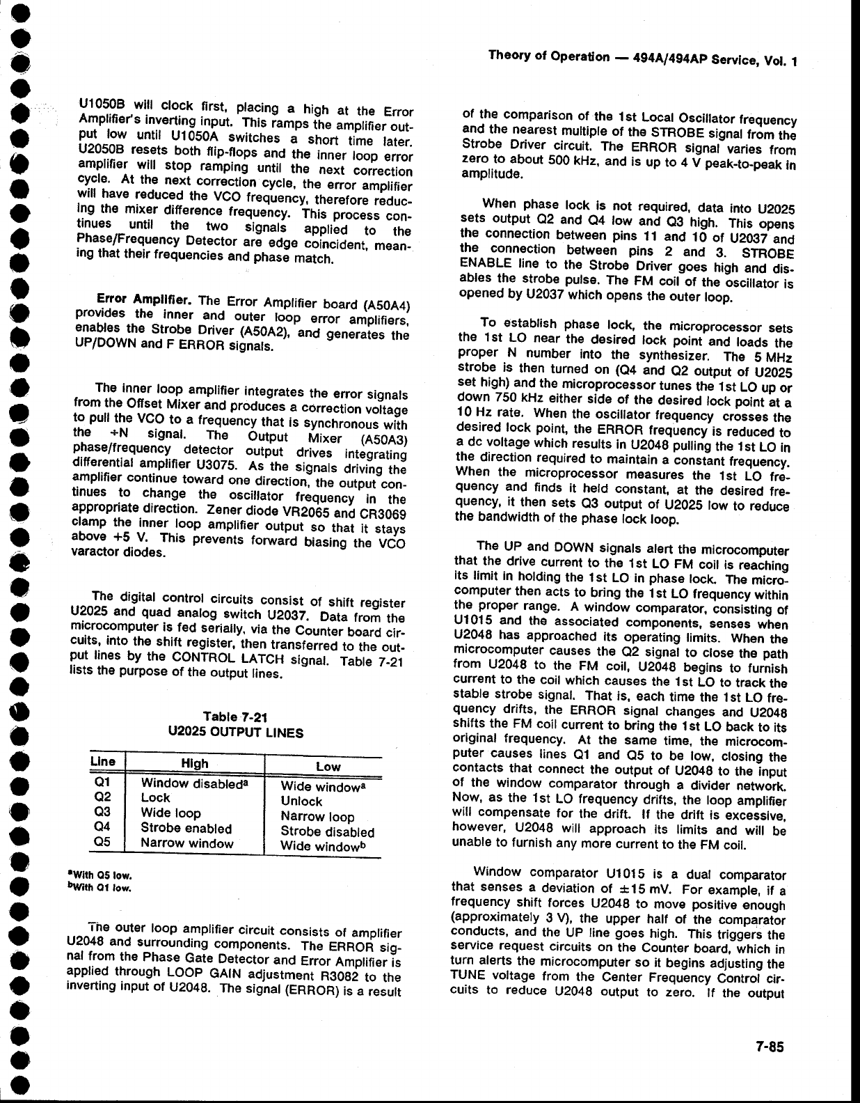
U10508
witt ctock first, placing
a high at the Error
Amptifier,s
inverting
input. This
iamps
it," "*ptiR", ort-
put low untit U1050A switches d "iiort time tater.
U20508
resets
both
flip-flops
anO
tne inner
toop
error
amprifier
wiil stop rampin! untir the next correction
cycle. At the next col-1clion cycle, the error amplifier
will have
reduced
the VCO
freqfuency,
it "i"for reduc-
ing the mixer
difference
frequen.y. fnl.-proceEs
con-
tinues untit the two signati appfilO to the
lh".:"/F.r."q.uency
Detector
ar6 eOge
"6ilcioent, mean-
ing
that
their
frequencies
and
ptras6
,"i"t.
Error
Ampilfier.
The.Eror Amptifier
boarct
(A50A4)
provides
the inner 3F oglgl robp error amptifiErs,
enables
the Strobe
Driver
(A5OA2),'and
generates
the
UP/DOWN
and
F ERROR
signals.
, The
inn-er
loop amplifier
integrates
the error
signals
from
the
Offset
Mixer and
produJes
a cJriection
vottage
to pull
the VCO
to a frequency
that
is synchronous
with
t!" -r-[rl signat. Th€ Output f"rii", (A5OA3)
phasefrequency
dete-cJor
output drives integrating
diff€r.entiat
amptifier
U3075. As the signais
driving
the
amplifier
continue
toward
one
directionl
the
output
con_
tinues !o change the oscillator frequency in the
appropriate
direction.
Zener
diode
VR2O6S
and
CRgO6g
glamp
tl: jgel loon amptifier
output
io $,"t it stays
abovg +5..
V. This prevents tonrrard biasing th€ VCO
varactor
diodes.
. - _4. digital
control
circuits
consist
of shift register
U2025
and quad
anatog
switch U2Og7.
Data
trom
the
microcomput.r
is fed
seriaily.
via
th€
counter
board
cir-
cuits,
into.the.shiftregister,
then
transfer;; to the out-
put fines
by the CONTROL
LATCH
signat. Tabte
T-21
lists
the
purpose
of the output
lines.
rWith OS low.
bwit ot tow.
..-^fl" outer
loop
amplifier
circuit
consists
of amplifier
U2048
and
surrounding
components.
The ERROd
sig_
nal
from
the
phase
Gate
Detector
and Error
Amplifier
is
applied
through
LOOP
GAIN
adjustment
R0082
to the
inverting
input
of U2O4g.
The
signal
(ERROR)
is a result
Theory
of Operation
- 4g4ful4g4Ap
Service,
Vol. 1
of the comparison
of th€ 1st Local
Oscillator
frequency
and
the
nearest
muttiple
of th€
STROBE
signat
trdm
tn6
Strobe Driver
circuit.
The ERROR
signat
varies
from
zero to about S00
kHz,
and is up to 4 V peakto-peak
in
amplitud€.
When
phase
lock is not required,
data
into U2OZ'
sets output
e2 and
e4 tow and e3 high. This
op"ni
the connection
between
pins 11 and ld of U20g7and
the connection
between pins 2 and 3. STROBE
ENABLE
tine
to th€ Strob€
Driver goes high
and dis-
ables
the strobe
pulse.
The FM coil
of the oscillator
is
opened
by U2A37
which
opens
the outer
toop.
.. lo establish
phase
lock, th€ microproc€ssor
sets
the lst LO near
the d€sired
lock point
and loads
the
proper N number
into the synthesizer.
The S MHz
strobe is then turned on (e4 and e2 output ot U2025
set high)
and
the
microprocessor
tunes
the 1st
LO
up or
down
750
kHz
either
side
of the
desired
tock
point
Lt a
10
Hz rate. When
the oscillator
frequency
crosses
the
desired
lock
point,
the
ERROR
frequency'is
reduced
to
a dc voltage
which
resutts
in U204g
puiling
the 1st
LO
in
th_e
direction
required
to maintain
a consiant
frequency.
When the microprocessor
measures
the lst LO fr€-
quency
and finds
it hetd
constant,
at the desired
fre_
quencyr
it then
sets
Q3 output
ot u2025low to reduce
the
bandwidth
of the
phase
tock
toop.
The
UP and
DOWN
signats
alert
th€
microcomputer
that the drive
current
to th€ 1st Lo FM coil
is reaining
its limit
in holding
the
1st LO in phase
lock The
microl
computer
then acts
to bring
the 1st
LO
frequency
within
llt:-?pper range. A window
comparator,
ionsiittng ot
U1015
and thg associated
components,
sens€s
when
U2048
has approached
its operating
limits. When
the
microcomputer
causes
the e2 signai
to close
the path
from U2048
to the FM coil, U2O4g
begins
to fumish
current
to the
coil
which
causes
the
1st
LO
to track
the
stable
strobe
signal.
That
is, each
time
the 1st
Lo fre_
quency
drifts, the ERROR
signal
changes
and U204g
shifts
the FM
coil
cunent
to bring
th€ lst LO
back
to its
original
frequency.
At the same
time, the microcom-
puter causes
lines
el and e5 to be low, closing
the
contacts
that connect
the output
of u204g
to the input
of the window
comparator
through
a divider network.
Now,
as the l st LO frequency
drifts,
the loop
amplifier
will compensate
for the drift. lf the drift is excessive,
however,
V2048
will approach
its limits and wiil be
unable
to furnish
any
more
current
to the FM
coil.
_ Window comparator
U101S
is a dual comparator
that senses
a deviation
of *15 mV. For example,
if a
frequency
shift forces
U2049
to move
positive
enough
(approximately
3 V),
the upper half of the comparator
conducts,
and
the Up line
goes
high. This
triggers
the
service
request
circuits
on the Counter
board.
which
in
turn alerts
the
microcomputer
so it begins adjusting
the
TUNE
voltage
from the Center
Frequency
iontroi cir-
cuits to reduce U204A output to zero. lf the output
Tabte
7-21
U2025
OUTPUT
LINES
Llne
Q1
Q2
Q3
Q4
Q5
Low
Wide
windowa
Unlock
Narrow
loop
Strobe
disabled
Wide
windowb
Window
disabteda
Lock
Wide
loop
Strobe
enabled
Narrow
window
7-85
Theory
of Operation
- 4g4[l494fup
Servlce,
Vol. 1
drifts
negative,
the other
half of UlO.l5 conducts,
caus_
ing
reverse
action
to occur.
- Normally,
the
input
signal
to the
window
comparator
is attenuat€d
by R2040,
which reduces
the voltage
applied
to U101S
to 0.9% of the output
from U204-g.
This allows
U2048
to drift up
and down
without
immedi-
ately triggering
either comparator.
when R2043
is in
the circuit,
it is called
,'wide
window,'operation.
When
phase
lock is de-selected,
the microcomputer
selects
narrow window (which bypasses R2049). The Center
Frequency
Controt
circuit is then instiucted
by the
microcomputer
to move
the 1st LO frequency
uniit
tne
window
comparator
indicates
that the FM
coil
current
is
near zero. This prevents
the lst LO frequency
from
shifting
too far from
the lock point
when
phase
lock is
canceled.
The F ERROR
signal
is used
by the
Counter
board
(A51)
for diagnostics
so that the microcomputer
can
determine
the relationship
between
.t
st LO irequency
and the strob€
line.
The F ERROR
signal
is generatei
from
thE
outer
loop
ERROR
signal
from
the
phase
Gate
Detector (A24). The circuit
consists
of an active
low-
pass
filter U2065
and Schmitt
trigger
U1Og5.
This cir-
cuit ftlters
and squares
the incoming
ERROR
signal.
The ERROR
signat
is apptied
through
CZO67
to an nC
500 kHz
low-pass
filter
and
amptifier
U2O6S.
After
fitter-
ing, the signal
is applied
through
Enor Count
Break_
point
adjustment
Rl061 to the input of u1035,
a schmitt
trigger circuit. The squared output signal is then
applied
to circuits
on
the
Counter
board.
The STROBE
ENABLE
signat
enabtes
the strobe
generator
in the Strobe Driver circuit (ASOA2).
Shift
register
U2025
reads
the instrument
bus latch
on the
counter board (A51)
to determine
the status of the
STROBE
ENABLE
signat. O20gO
inverts
the signat
and
converts
it to TTL
level
to drive
the
strobe
generator.
controlted
oscillator
(vcol. The controiled
oscilla-
tor (VCO) is a voltage-controlled
crystal oscillator
whose
frequency
is controlled
by
the
output
of the Error
Ampllfier. The oscillator generates
a reference
signal
that as
used
to stabilize
the lst LO frequency.
Refel
to
the block diagram
adjacent
to Diagram
40 for a func_
tional
description
of this
part.
The control
voltage
from the Error Amplifier,
which
is a function
of th€ difierence
between
the microcom-
puter controlled +N signal and the Offset Mixer
difference
frequency,
is applied
to the
VCO
on
the
Con-
trolled Oscillator
board to regulate
its frequency
of
operation.
The circuit
has
two outputs:
the first,
which
is part
of the
inner
loop
of the
phase
lock
circuits,
is fed
to the Offset Mixer, where it is used to derive the
difference
frequency
that is compared
against
the +N
signal. The second
output,
which
is part of the outer
loop, is led to the Strobe Driver
circuits.
where it is
7-86
divided
down to becomE
th€ STROBE
signal
that is
compared
against
the l st LO signal
in
the phase
Gate.
The VCO consists of five major circuits,
four of
which
are
connected in a positive
feedback
loop
to sus-
tain oscillation.
These circuits
ar€
the resonator
stage,
the differential
amplifier,
the bandpass
lilter,
the isola-
tion amplifier,
and the output amplifier.
The resonator
stage operates at a frequency ot 2S.OS2MHZ
to
25.094
MHz. Th€ output signal
from the resonator
is
applied
to the input of a differential
amplifier
which
drives
the output amplifier
and
the
bandpass
filter. The
output from the output amplifier
is fed to the Offset
Mixer and the Strobe Driver.
The bandpass
filter strips
the signal of any spurii €ither
side of csnter
frequency
and feeds th€ signal to the isolation
amplifier. This
stage
furnishes
the positive
feedback
drive
to the
reso-
nator stage and isolates the bandpass
filter from the
resonator
stage.
The resonator stage consists of crystal y1012,
varactor
diodes
CR1011
ancl
CRl012,
and r€lated
com-
ponents. The stage operates within the frequency
range of 25.032
MHz
to 25.094
MHz,
which is
controil€d
by the voltage applied
to varactor
diodes
CR1011
and
cRl0l2. Feedback energy
for sustaining
oscillations
comes from
the
isolation
amplifier
by way of coil
Ll025.
The resonator output signal is applied to a
differential
amplifier
Q2033
and
Q2041. The
Q2033
side
drives
the output amplifier and serves
to isolate
the out-
put
load from
the feedback
loop. Gain from
this side is
less than one. The signal
is fed from the collector
of
Q2041, following
amplification,
to the band-pass filter.
The band-pass filter consists of passive com-
ponents,
and
is used
to strip
the
signal
of any frequency
components
more than about 40
kHz away from the
center operating frequency, which is approximately
25.06
MHz. Capacitors C1041 and
C1042 ar€ adjusted
at th€ factory
to set the bandwidth and cent€r
the fre-
quency
of the filter.
The isolation amptifier,
01028, is a common-base
configuration,
in order to match
the impedance
of the
filter to the resonator. Output current from the stage
furnishes
positive
feedback for
the
resonator.
The
output
amplifier. consisting of transistors Q2025
and
Q2026, is connected as a differential amplifier with
02026 driving
one side
of the Offset
Mixer and Q2025
driving
the input
of the
Strobe Driver circuit, for
eventual
application
to the
Phase
Gate
circuits.
Strobe
Drlver
Clrcult. The Strobe Driver circuit
con-
sists
of counter
U1022,
bandpass filter FL2064, sourc€
follower
02091
, and AND
gates
U1091A
and
U10918.
o
I
o
o
o
o
o
a
o
I
o
o
o
a
o
o
o
e
o
o
a
o
o
o
o
o
o
o
o
o
t
o
o
o
o
I
O
o
o
o
o
o
o
o
...Ttg V_CO
output
!g apptied
to the ctock
input
of
divide-by-s
counter
UaZZ. 'The STROBE'er.raeLe
fin"
frgm
tlte Error
Amplifier
permits
the
counter
to operate
when the line is low and is the means
by wnich
the
microcomputer
can turn the strobe pufsed on or off.
The .counter
output couples throug'h
an- impedance
matching
network
consisting
of Ce0i0, f_iOar,
C2Ogg,
and
C1032,
to the input
of blndpass
ntier
fLzOO+.
fne
1Tp"g11g"^
matching
circuit
raises
the
tine
impedance
to
about
8200
ohms.
Theory
ol Opera{on
- 4g4Al4S4Ap
Servtce,
Vol. 1
The output of the fitter
drives
another
impedance
matching
network
for the
gat€
input
of e2091. The
out-
put of Q2091
drives
two buffer
amplifiers
Ut091A
and
U10918. Ul0918 drives
the phase
Gate
circuitry.
and
Ul091A is reserved
for future
applications.
Capicitors
Cl032 and
C2105 ar€
s_elected
to provide
maximum
sig_
nal
amplitude
at TP20BZ.
7-87
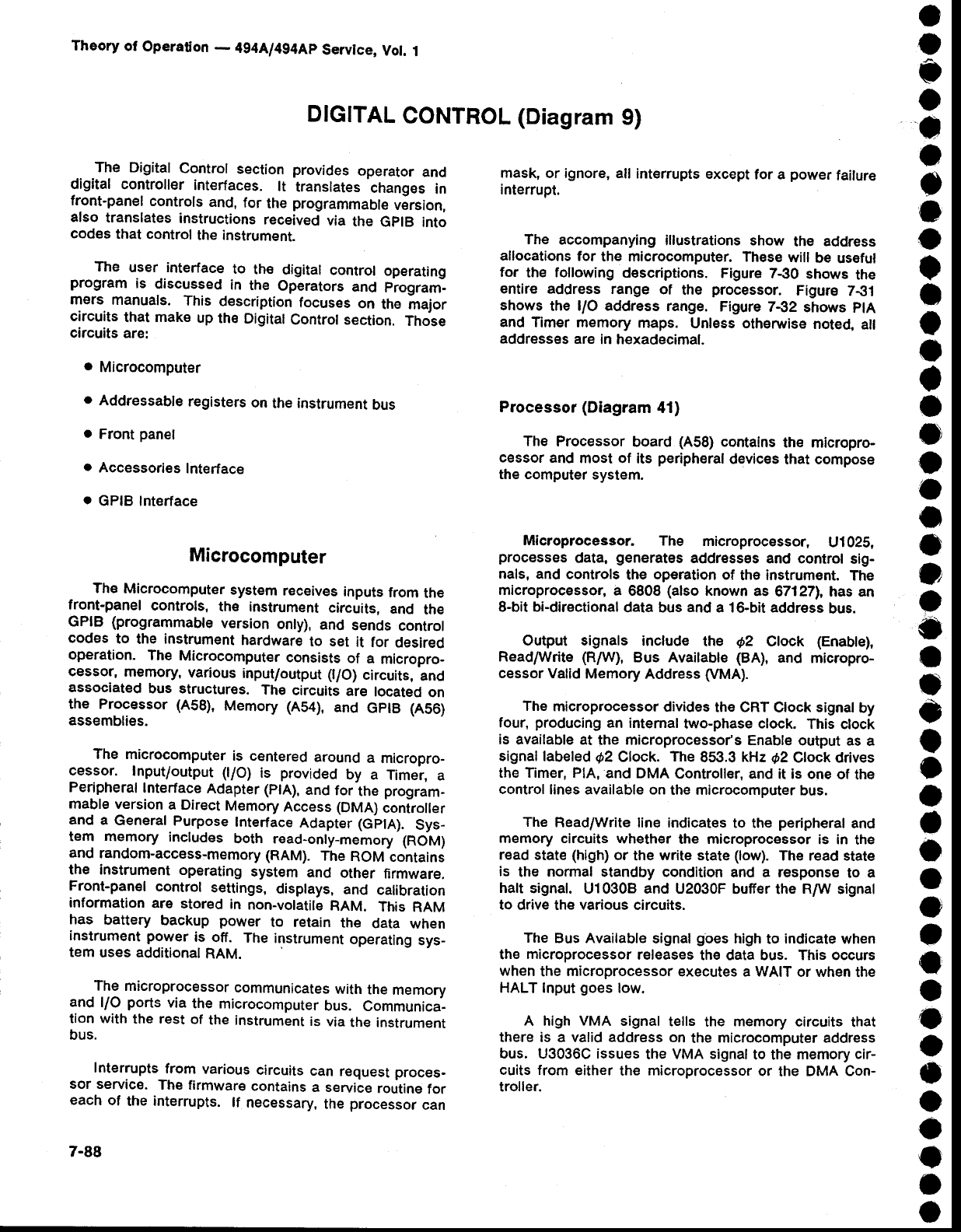
DIGITAL
CONTROL (Diagram
9)
The Digital
Control
section provides
operator
and
digital controller
interfaces. lt translates
changes
in
front-panel
controls
and,
for the
programmable
version,
also translates
instructions
received
via the GplB into
codes
that control
the
instrument.
The user interface
to th€ digital
control
operating
program
is discussed
in the Operators
and program-
mers manuals.
This description
focuses
on the rnajor
circuits
that
make
up
th€
Digital
Control
section.
Those
circuits
are:
. Microcomputer
o Addressable
registers
on
the instrument
bus
. Front
panel
o Accessories
Interface
o GPIB Interface
Microcomputer
ThE
Microcomputer
system
receives
inputs
from
the
front-panel
controls,
the instrument
circuits,
and the
GPIB (programmable
version
onty),
and sends
control
codes
to the instrument
hardware
to set it for desired
operation.
The Microcomputer
consists
of a micropro_
cessor,
memory,
various
input/output
(l/O)
circuits,
and
associated
bus structures.
The
circuits
are located
on
the Processor (A58),
Memory
(A54),
and GptB (A56)
assemblies.
The microcomputer
is centered
around
a micropro-
cessor. Input/output
(l/O) is provided
by a Timer,
a
Peripheral
Interface
Adapter
(plA),
and
for the
program-
mable version
a Direct
Memory
Access (DMA)
ioniroller
and a General
Purpose
lnterface
Adapter
(GFIA).
Sys_
tem memory includes
both read-only-memory
(ROM)
and
random-dcc€sS:rn€mory
(RAM).
The
ROM
contains
the instrument
operating
syst€m
and other firmware.
Front-pan€l
control s€ttings,
displays,
and calibration
information
are stored
in non-volatile
RAM. This
RAM
has battery backup power to retain the data when
instrument
power
is off. The
instrument
operating
sys_
tem
uses additionat
RAM.
The
microprocessor
communicates
with
the
memory
and l/O ports
via
the microcomputer
bus. Communica-
tion with
the rest
of
the
instrument
is
via
the instrument
bus.
Interrupts
from various
circuits
can
request
proces-
sor service.
The firmware
contains
a service
routine
for
each
of the interrupts.
lf necessary,
the
processor
can
7-88
Theory
of Operation
- 494[l4g4Ap Service,
Vot.
1
mask,
or ignore, all interrupts
except
for
a power
failure
interrupt.
The accompanying
illustrations show the address
allocations
for the microcomputer.
These
will be useful
for the following
descriptions.
Figure
7€0 shows
the
entire address range of the processor. Figure
7-31
shows
th€ l/O address
range. Figure
7€2 shows
plA
and Timer memory
maps. Unless othewyise
noted,
all
addresses
are
in hexadecimal.
Processor
(Diagram
41)
The Processor
board (A58)
contains
the micropro-
cessor
and
most of its peripheral
devices
that compose
thE computer
system.
Microprocessor. The microprocessor, Ul025,
processes
datai generates
addresses
and control
sig-
nals,
and
controls
the operation
of the instrument.
The
microprocessor,
a 6808
(also
known
as 671271, has an
8-bit bi-directional
data
bus
and
a 16-bit address
bus.
Output signals include the 02 Clock (Enable),
ReadfA/rite (R/W), Bus Available (BA), and micropro-
cessor Valid
Memory
Address
(VMA).
The
microprocessor
divides
the CRT
Clock
signal
by
four,
producing
an intemal
two-phase
clock. This
clock
is available at the microprocessor's
Enable
output as
a
signal
f abeled
d2 Clock. The
853.3
kHz
02 Clock drives
the Timer, PlA,
and DMA
Controller,
and it is one
of the
control
lines available on
the microcomputer
bus.
The Read/Write
line indicates
to the peripheral
and
memory circuits
wheth€r
the microproc€ssor
is in the
r€ad
state
(high)
or the write state
(low). The read state
is the normal
standby condition
and a response
to a
halt signal. U10308 and U2030F
buffer the R/W
signal
to drive the various circuits.
The
Bus Available
signal
goes
high
to indicate
when
the microprocessor
releases
th€ data bus. This occurs
when
the microprocessor
executes a WAIT
or when
the
HALT lnput
goes
low.
A high VMA signal tells the memory
circuits
that
the,re is a valid address on
the microcomputer address
bus. U3036C
issues
the VMA signal
to the
memory
cir-
cuits from either
the microprocessor
or the DMA Con-
troller.
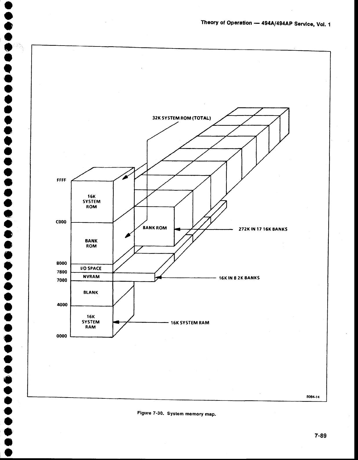
Theory
of Operation
- 4g4Ll4g4Ap
Servlce,
Vol. 1
o
o
o
o
o
o
I
o
o
o
I
t
o
o
o
o
o
t
o
a
o
o
3
O
o
t
t
o
I
o
o
o
o
I
t
o
o
o
a
o
o
)
o
o
8000
7800
7000
4000
0000
Figure 7-30. System memory map-
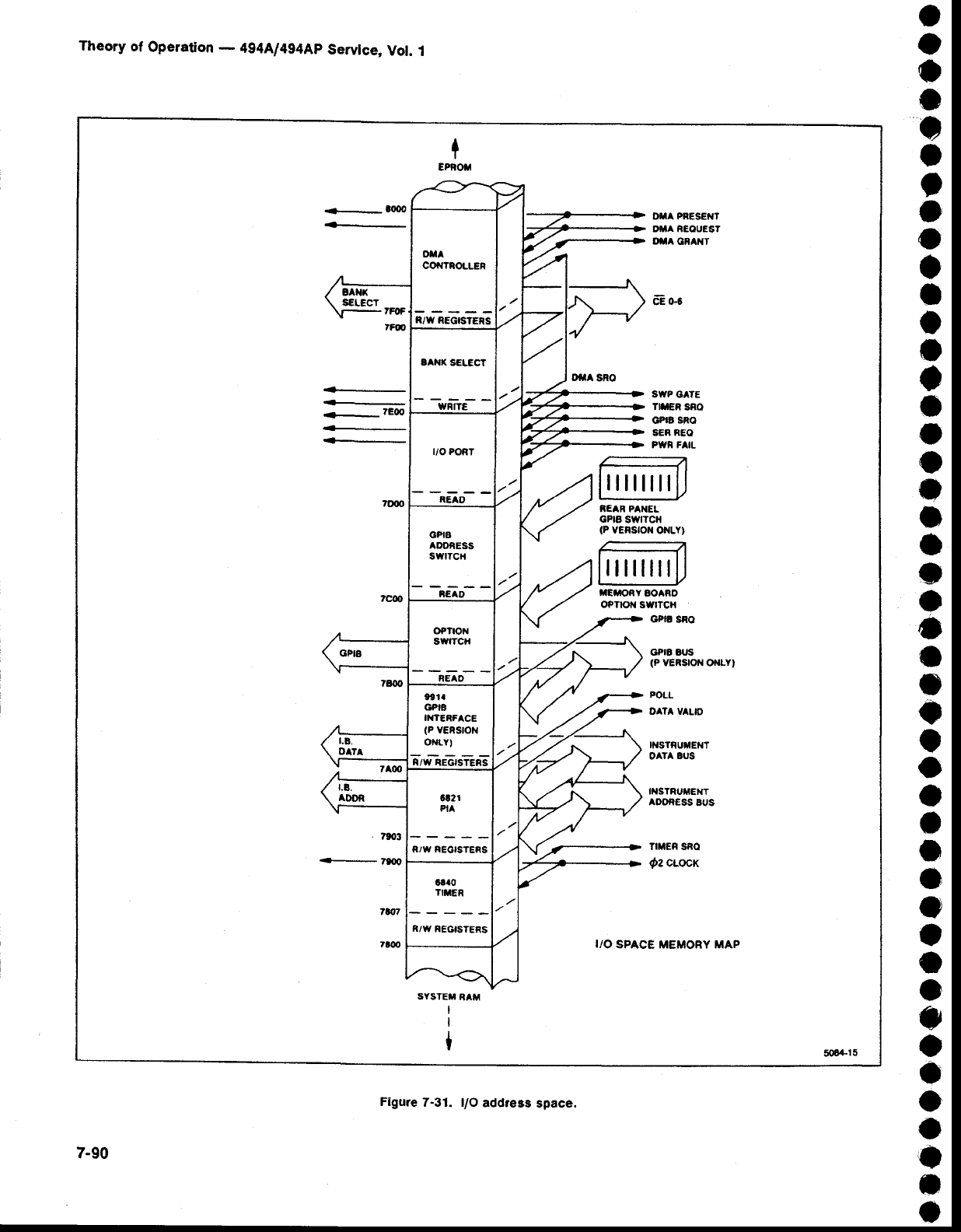
Theory
of Operation
- 494A/494Ap
Servlce,
Vol. 1
DTA PFESENT
DT REOUEST
ilA GRANT
feoc
SWP CATE
TMER
sNO
oPrg sRo
SER RgO
PWR FAIL
lililililll
NEAR PANEL
GP|a SIVITCH
(P VERStOfl
ONLYI
-__ ,-7
Llllllull,l
ITISTRUTE'{T
oATA 8US
INSTRUTIEilT
AOOfi€SS
aus
TIMEN SRO
02 CLocK
I/O SPACE MEMORY MAP
+
EPnoti
SYSTET fiA'U
I
I
I
?
+-
-- 7E@
+--+
+---
Figure
7-31. UO
addr€ss
space.
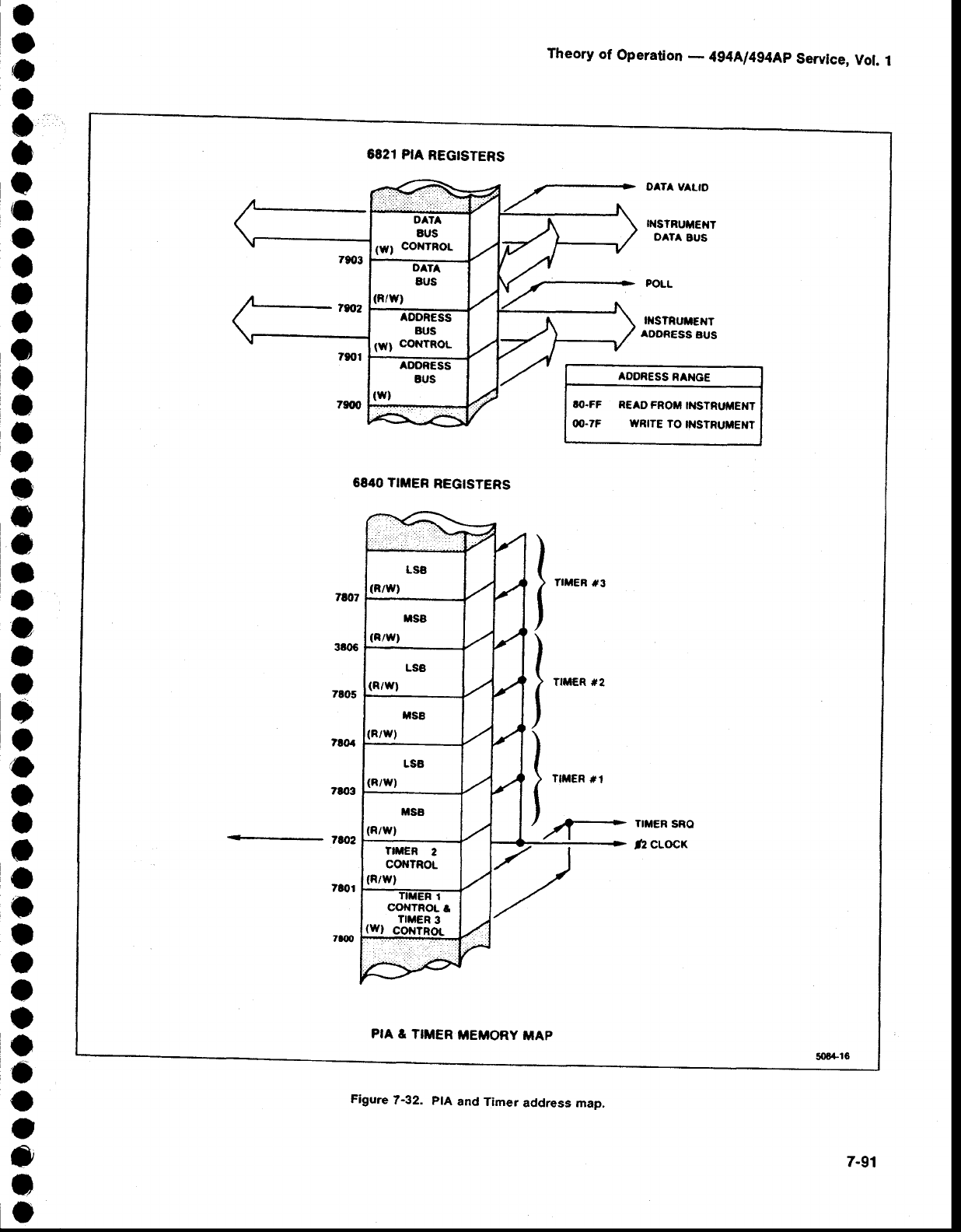
o
o
o
o
o
o
a
o
o
a
I
o
o
I
a
o
t
o
o
o
O
a
o
a
o
t
o
o
o
I
o
o
o
I
o
o
t
o
a
o
o
c
o
I
Theory
of Operation
- 4g4hl4g4Ap
Service,
Vol.
1
Figure 7-32. PIA and Timer address map,
6821
PIA
REGTSTERS
OATA VALID
0{sTRUt|€XT
D^TA AUS
POLL
II{STRUTIENT
AOOR€SS
BUS
AODRESS
RANGE
!O.FF N€ADFROT'NSTRUilEilT
(n-7F WR|TE
TO tilSTRUit€ltT
6840 TIMER
REGISTERS
PIA
& TIMER
T'EMORY
iIAP
7903
7CUl

Theory of Operation
- 494A/4g4Ap
Service,
Vol. 1
Clock. This circuit
generates
the clock
signat
that
drives
the microprocessor,
the GplA transceivdr
on the
GPIB board
(A56),
and
the character generator
circuitry
on
the
CRT
Readout
board (A66A1).
Y1030,
Q2035,
and e1030 form a clock
circuit
that
oscillates
at 3.4133
MHz. e2095 and y1030 form a
Colpitts
oscillator
and el030 buffers
the output, giving
a TTL compatibte
ctock signat. This signat
is turtnei
buffered by
U2030A
forming
th€ crt clock
signat.
Mlcrocomputer
Bus. Microcomputer
communica-
tion with memory
and l/O is via
the microcomputer
bus.
The bus consists
of eight data tines (D0-Dti),
sixteen
address
lines
(A0-A15),
the RESET
tine,
the
VMA (Vatid
Memory Address)
tine.
the Read/Write
(R/W)
tine,
and
the
62 Clock.
The data lines connect from the microprocessor
through bi-directional
buffer VZ02S. The Read/Write
line controls
data direction
through
the buffer, When
the microprocessor
releases
the address
bus,
the Bus
Available
line
(BA)
disables
the
data
bus
buffers
through
U3036A. Jumper
P3015
is a test jumper
that ailows
disabling the data buffer and forcing
a CLR
B instruc-
tion to the microprocessor. Diodes CR2O20
and
CR2025
pull
data
tines
MDS and MD7
tow,
issuing
the
CLR B instruction.
The address
lines
connect
from
the microprocessor
through buffers
U3030 and U302S. These
buffers
are
disabled when the DMA Controller is granted the
address
bus. Then
the addresses
come
from
the
DMA
Controller,
U1020,
through
DMA address
buffers
U1015
and U1024.
U1015 is a bi-directionat
bufier,
allowing
the
microprocessor
to address
the
DMA
Controiler.
The RESET
signal
is a function
of the
power
Failure
circuit. When
a power
failure
is sensed,
the
RESET
sig_
nal resets the
Timer,
PlA, DMA Controlter.
and
circuits
on the Memory
(A54)
and cptB (A56)
boards, The
Power
Fail circuit
is discussed
in more
detail
later. The
VMA, R/W, and 02 Ctock signats
have atready
been
described.
Address
Decoder. AU303S
decodes
the
addresses
for the l/O circuits
on this board. When
the micropro-
cessor
selects
an address
in the range
of 7g00-7FFF.
the l/O line from the Memory board (A54)
goes low,
enabling U3035. The decoder then subdivides
the
address range to select each circuit. Figure 7-3.1
shows
the
UO
address
map. Each circuit
uses
only
one
or a lew addresses
within
its range.
7-92
Tlmer. The
Timer
circuit,
U2015, is a 6840
program-
mable
timer used by the microprocessor
to generate
variable
time
delays. The
processor programs
an
inter-
val into
the timer. When
the interval
passes,
the
Timer
generates
an interrupt
fl-imer
SRA). The
{2 Clock syn-
chronizes the Timer with the microprocessor. An
address
in the
timer range selects
the Timer. Address
bits A0-A2 select
internal Timer
registers,
count€rs,
and
latches. When the ReadfAlrite (RfA/) line is low, the
Timer accepts
data
input from the data
bus. When
the
line is high,
the Timer puts its data on the data bus.
See
a 6840
data sheet tor additional details. The Timer
addressing is
mapped in Figure 7€2.
PIA and Instrument Bue. The microcomputer
com-
municates with the instrument
through the lnstrument
Bus.
The
6821 PlA,
U1010,
interfaces
the
DigitalControl
circuits
to the Instrument
Bus. This
bus contains
eight
data lines
(DBO-DB7),
eight address lines (AB0-A84,
the DATA
VALID
line,
the
Service
Request
(SER
REQ or
SR) line, and
the
POLL line, allthrough
the PlA.
The PIA
receives Read/'li/rite,
02 Clock,
and RESET
control signals
from the microprocessor. Figure
7-32
shows the
PIA
address
map.
The
address
lines are buffered by U3015. The data
lines are buffered
by bi-directional
buffer U3010. The
buffer is gated on when data is valid. The most
significant address
bit selects data direction so
that
half
of the address
space is for writing
to the instrument,
and half is for reading from the instrument. The PIA
CB2
port
(U1010
pin
19)
goes
low when
the data on
the
lnstrument Bus is valid. Resistor-capacitor circuits
delay the DATA
VALID signal to the Instrument
Bus.
assuring
the proper
timing
relationship with the other
Instrument
Bus signals.
The
PIA issues
the POLL and DATA
VALIO
(or
DV)
signals in response
to a service request from the
hardware on
the
Instrument Bus. The requesting circuit
responds
to the POLL signal on the Instrument
Data
Bus.
The Internal
Control
(INTL
CONT)
signal comes from
the
Accessories
Interface assembly
(A30A76).
This sig-
nal is normally high
unless
external
control
through
the
ACCESSORIES connector is desired. When
low,
the
Bus
Enable
signal
goes
high,
disabling
the address
and
data buffers
and the DATA VALID
and POLL outputs.
The Bus
Enable
jumper,
P3010, may be
removed
to
dis-
able
the
Instrument Bus for test
purposes.
DMA
Controller.
When the instrument
transfers
data
through
the GPIB
interface,
the DMA Controller,
Ul020,
sets up direct
transfers between
system RAM and the
a
o
a
a
a
a
o
o
a
o
o
I
o
o
a
I
)
o
o
o
o
,
o
I
o
o
t
o
I
I
I
a
o
o
o
o
o
o
o
o
a
o
I
o
GPIA
interface
circuit
on th€ GptB
board (A56). (Ihis
only
occurs
on
the
programmable
version.)
Before each transf€r, the microprocessor
loads
U1020
with the starting
address
of the RAM
data
and
the number
of data
bytes
to be
transferred.
When
the
GPIA interface
circuit requires
data,
it pulls the DMA
Request
line, pin 4 of pl03S,
low. This
iauses U1O30C
to set U1020's
Transferfiequest
input
high,
requesting
a byte. ln rEturn,
the DMA Controller
ienOs a DIUA
request
to the processor,s
HALT
input, pulling
it low.
This also
disables
any
maskabte
interrupt
iequest
to tne
processor. With HALT
low, the microprocessor
com-
pletes
its currenily
executing
Instruction
and
then
stops,
signals
that
the bus is avaitabte
(sets
the BA tine
high),
tri-states
its data bus, and
sets
itself
in the Read
stlte
(RflrV
line
high).
The BA signal
disables
the
rnicroprocessor
address
bufrers,
U3030
and
U302S,
and
enables
DMA
Controller
access
to the address
bus via buffer
U1024
and tran_
sceiver
U1015. lt also gives
bus
control
to the DMA
Controller.
The
least
significant
address
lines
are
inter-
faced
to Ul020 through
a transceiver
because
the pro-
cessor
uses
addresses
A0 through
A4 to address
the
setup
registers
in
the
DMA
controller.
The DMA Controller
sets th€ address,
VMA, and
ReadfA/rite
(RflrV)
lines
to caus€
the RAM
to plac€
the
proper byte on the data bus. Because
U10b0 is an
open-collector
gate, there is no conflict
between
the
microprocessor
and the DMA
Controller
over the R/W
line.
The DMA
Controiler
Transfer
Strobe
tIxSTB)
output
goes
low
giving
the
DMA
GRANT
signalto
tne
eFte fir_
cuit on the GPIB board. This infoims
the circuit
that
data is coming.
After
the
transfer
is completed,
UlO20
raises
the HALT line,
and normal processor
operation
resumes.
Ground
from
the
GplB
board
connects
through
pin
2
of P1035 as a signal that the processor
and GplB
boards are connected. lf the GplB board is not
present,
such
as
for
test
purposesr
U10gSB
pin
12
goes
low. This
disables
the DMA
request.
Interrupt Processing. The microprocessor
uses
both
maskable
and non-maskable
interrupts.
The
non_
rnaskable
interrupt
is used
only
for sensing
power-fail.
The maskable interrupt is used to seise circuits
requesting
service.
Although
these
interrupts
may be
rnasked
by
the processor,
they are
enabled
most
of the
time. These
interrupts
can
be requested
bv circuits
on
the Instrument
Bus, the GplB board,
the DMA
con-
troller,
or the Timer. The
instrument
firmware
contains
Theory
of Operation
- 494A/4g4Ap
Servlce,
Vol, I
service
routines
for each
of the
interrupts.
The maskable interrupts are sensed at the
microprocessor's
Interrupt
Request
(lRQ)
input. Gate
u2036 sets IRQ low if it senses
any of the int€rrupt
lines
low. The
Input
port buffer
U3O2O
places
the inter-
rupt infornation
and
swe€p
anformation
on
the data
bus.
This allows
the microproc€ssor
to read the int€rrupt
status.
lf the interupt is from circuits
on the Instrument
Bus, the microprocessor
executes
a poll routine
to
determine
the
exact cause
of the interrupt.
The Instru-
ment Bus circuits
interrupt
the microprocessor
by pul_
ling the Service
Request
(SER REO or SR) tine
tow.
The microprocessor
responds
by placing
address
FF
on
the Instrument
Bus and setting
the OATA
VALID
anct
POLL signals high. This causes the circuit that
requested
service
to pull
one of the
data
lines
low.
Each circuit
is assigned
a different
line,
as
shown
in
Table
7-22. lt is possible
that more than one circuit
requ€sts
service
at th€ same
time. In that case.
more
than
one
data line
will
be low.
The microprocessor
reads
the data lines
to deter_
mine
the interrupting
circuit
or circuits. tt then writes
the coresponding
bit pattern
to the
data
bus whil€
the
address
lines
are
set
to ZF and
DATA
VALID
and
pOLL
are both high. When
an interrupting
circuit
receives
a
low on its assigned
data line with the address
lines,
DATA
VALID.
and POLL
set as described,
it rgsets
its
internal
interrupt
latch
and releases
the
Service Request
(sets
sER
REQ
or
SR high).
Table 7-22
POLL
BITS
0
Not Used
Not Used
Not Used
End of Sweep
FREQUENCY
knob
Phase Lock
Not
Used
Front Panel
The
non-maskable
interrupt
signals
power
loss. Cir-
cuitry on the Z-Axis
assembly
(A70)
senses
power
loss
and
sets
the
PWR
FAIL
line
low. This causes
an inter-
rupt and starts
the microprocessor's power
fail
routine.
Wh€n PWR FAIL goes low, e2030 turns on and
C2030
begins
to discharge
through
Rl032. tf the
tine
stays
low until
C2030
discharges,
the RESET
line
goes
low
and
the
microprocessor
res€ts
itself. As part
of its
power fail routing,
the microprocessor
monitors
the
PWR
FAIL, along
with
other interupts, through
U9020.
Bit 7
Bit
6
Bit
5
Bit
4
Bit
3
Bit
2
Bit
1
7-93
Theory of Operation
- 494Al4g4Ap
Service,
Vol. 1
lf the PwR FAIL
line returns
to a high state
before
the
microprocessor
is reset, the microprocessor
does a
power-up initialization
to ensure that the instrument
operation will not be affected
by a temporary
power
loss.
This power
fail
sequence
can
be disabled
by remov-
ing
jumper
W2035. This
may
prevent
lalse
resets
when
operating
the instrument
on noisy power. However,
power-down
settings
will
not
be stored.
Memory (Diagram 42)
The M€mory
board
(A54)
contains
some
of the
ROM
and all of the RAM
used
by the microprocessor.
There
are 64Kr bytes
of ROM
in two g2K byte EpROMs
and
32K bytes of RAM in four 8K byte RAMs. Battery
backup power is supplied
for 16K of the RAM. The
board also contains
the Options switch, which sets
some instrument operations
and selects
processor
test
modes. Additional
ROM
is located
on the
GplB board
(As6),
Address Decoders.
The address
decoding
circuits
rnonitor
the
microcomputer
bus to enable circuits
on
the
board. Decoder
U2045
is the main address
decoder,
selecting four
16K-byte
blocks
of address
space:
0000€FFF for RAM
4000-7FFF for NVRAM
and t/O
8000-BFFF for Bank ROM
C000-FFFF for system
ROM
The upper half of U2045
decodes
the non-volatile
RAM
and l/O space. The lower half decodes
th€ system
RAM and
the ROM space. The
OZ
Clock signal
ctocks
the lower
half of U2045
to assure
proper
memory
tim-
ing.
The system
RAM address space
is the 16K bytes
from 0000€FFF. The 2K space from 7000-77FF
is
switched b€tween eight 2K banks of the 16K non-
volatile RAM.
The system
RAM
address space
is divided
between
two 8K RAMs, U101O
and U3020.
The lower
half of
U2045, U3030C, and U3030D
enabte
U1010 for the
address
space
between
0000
and 1FFF.
The
lower half
of U2045 and the upper half of U3025 decode
addresses from
2000€FFF.
This enables
U3020.
The non-volatile
RAM
is bank
switched
into
eight 2K
banks
addressed from
7000
throughTTFF.
This
allows
more
rnemory
than the processor
can
directly
address.
At address
7E00,
the bank select circuit
on the GplB
board (456)
enables
tatch
U4020. The tatch
hotds
the
lx-m;o24-
7-94
RAM bank number from bits D+D7 of the microcom-
puter
data bus.
LatchEd
bit D7.
tne
62 and
the
7000 address
enable
from the upper
half of decoder U3025 drive the lower
haff
of U3025
for the 7OA0-77FF addr€ss space. lf D7
is low,
U1030 is
enablEd; if hlgh,
Ul020
is enabled.
The
other
two bank
select bits,
D5 and
D6, directly drive
two
address
lines,
creating four banks in each of the 8K
RAMs.
The l/O space is decoded
by the upper half of
U2045, U3040,
and U3045. The upper
half of U2045
enables
U3040
for addresses from 7000-7FFF.
U3040
then decodes the
7800-7FFF
address tor Options circuit
and other
l/O space. This llne
is sent
off the board
as
the l/O signal. The Options
circuit is addressed at
7800
by U3045.
ROM address decoding
is performed
by the lower
half of U2045, data bit D4, some
gates,
and the bank
select circuits on the GPIB board
(A56). Half of ROM
U3050
is addressed
as bank
ROM
from address
8000
through
7FFF. The
other half
of U3050
is systern
ROM
addressed at C000 through FFFF. The bank ROM
address space is shared
with 16 other ROM banks.
Latch U4020
stores data bit D4 at address
7E00
{Bank
enable). When that bit is high, and when ths ROM
banks
are addressed, U3050
is selected. The latched
bit enables
U3050
through
U3030D.
For system ROM
addresses,
thg CXXX enable through U3030C and
U3030D,
and through U2040C
and U2040D
enables
u3050.
U3060
is selected
as banks 0 and 1 by the bank
select circuit on the ROM Banks and
GPIB
board
(A56).
The upper
and lower addresses are selected by data bit
D0 latch€d
by uao20 at address
7E00.
RAM. The RAM is divided
into systern
RAM and
non-volatile RAM. The
microcomputer uses the system
RAM for interim data storage while the instrument
is
operatang. The non-volatile
RAM stores changeable
data
such as waveforms,
readouts, and front-panel
set-
ups. The non-volatile
data is backed up by battery
power
when the
instrument
is not operating.
U1010 and U3020 form th€ main system RAM.
Each
lC contains 8K bytes
of RAM,
making
16K
bytes
totalsystem
RAM.
U1020
and U1030
form the battery-backed-up
non'
volatile RAM. When
the instrument
is operating,
these
RAMs are powered
by the +5 volt supply. When
the
instrument is not operating, the RAMs
are powered by
a
o
I
o
o
a
t
O
o
a
I
o
o
o
o
o
a
o
I
t
a
o
a
a
o
I
o
o
a
o
I
o
o
o
o
o
a
o
o
o
o
o
I
o
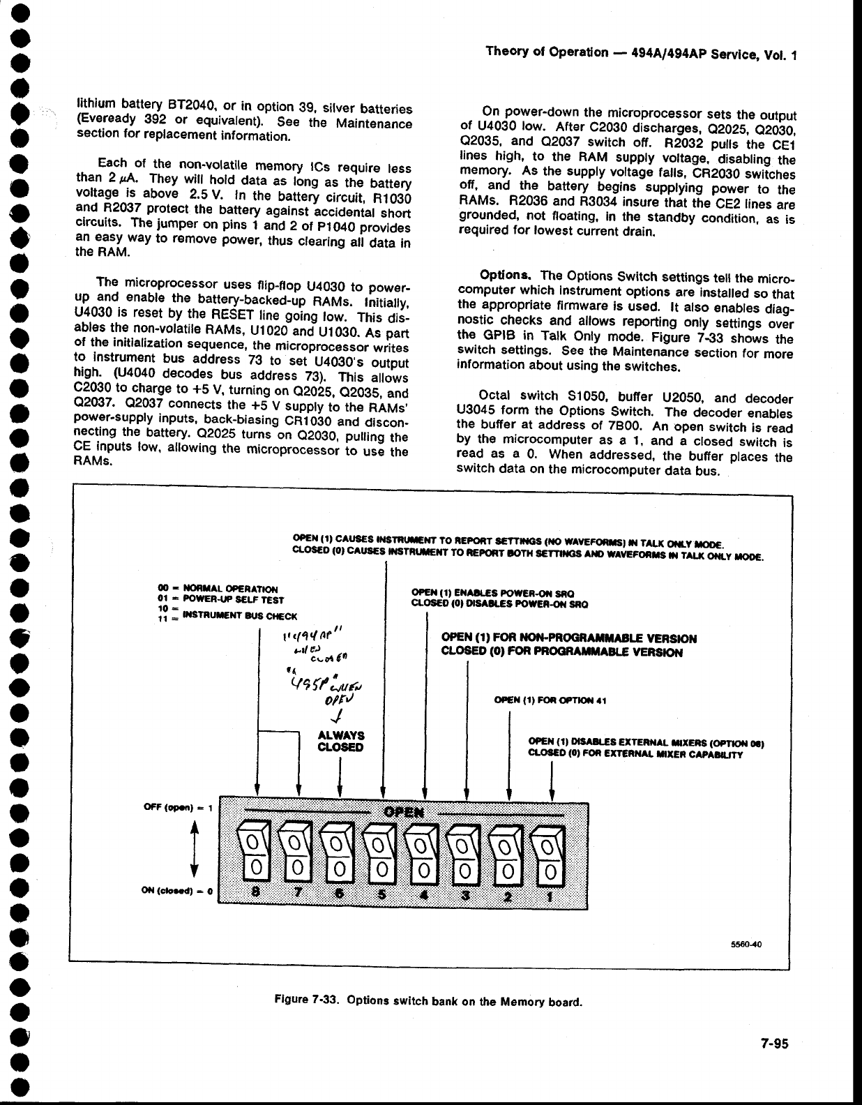
o
a
o
a
o
a
t
I
o
o
I
t
o
o
a
I
)
o
a
o
t
a
o
a
o
C
t
o
t
o
t
o
o
a
a
a
t
o
o
o
o
o
o
o
lithium
battery
8T2040,
or in option 3g, silver batteries
(Eveready
392 or equivalent).
See the Maintenance
section
for replacement
information.
Each
ol the non-volatile
memory
lcs require
less
than 2 rl. They wiil hold.
data as tong as the battery
voltage
is above 2.SV. In the batte{ circuit,
RIO3O
and R2037
protect
the battery
against;ccidental
short
circuits.
The
jumper
on
pins
i anO
e of p1040
provides
an easy
way
to rernove
power,
thus clearing
ali data in
the RAM.
The microprocessor
uses
ftip-flop
U4O3O
to power-
up and enabte
the battery-backed-up
RAMs. tnitiatty,
U4.030.is
reset
by the RESET
tine
goiog
tow. This
dis_
ables
the
non-volatit€
RAMs,
U1020
and-U1030.
As part
of the
_initialization
sequence,
the
microprocessor
writes
to instrument
bus address
73 to set U40gO,s
output
high. (U4040
decodes
bus address
73). This ailows
q?qq to^c-harge
to +5 V. turning
on e20i5. e2035, and
Q2CX!7.
Q2037
connects
the +5 V suppty
to th€ RAMS,
power-supply
inputs,
back-biasing
CRf03O
and
discon-
llcling the battery.
e202S
turns
on e2OgO,
puuing
the
CE inputs
low,
allowing
the micropro"e"soi
to use the
RAMs.
Theory of Operation
- 4g4Al4g4Ap
Service,
Vol.
1
On power-down
the microprocessor
sets
the
output
of U4030 low. After C2090
discharges,
e2O2S,
O20bO,
02035, and Q2037 switch off. R2Og2
puils the CE1
lines high, to the RAM suppty
vottage,
disabting
the
memory. As the suppty
vottags
fails,
CR2030
swiiches
9{, -and_
the battery begins supptying power to the
RAMs. R2036
and
R3034
insure
that
the-CE2
tines
are
grounded,
not floating,
in the standby condition,
as is
required
for lowest
current
drain.
Options. The Options
Switch settings
tell the micro-
cornputer
which
Instrument
options
are instaled
so
that
the appropriate
firmware
is used. lt also
enables
diag-
nostic checks
and allows
reporting
only settings
ovir
the GPIB in Tatk Only mode.
Figure
7€B shows
the
switch
settings.
See the
Maintenance
section
for more
information
about
using
the switches.
Octat switch S1050,
bufer U2050,
and decoder
U3045
form the Options
Switch. The decoder
enables
the buffer
at address
of 7800. An open
switch
is read
by the microcomputer
as a 1, and a closed
switch
is
read as a 0. When
addressed,
the buffer
places
the
switch
data
on
the microcomputer
data
bus.
OFEX (1' CAUS€S OISTRLn|CTT
TO IEPORT sG'T|r{CS (XC'
WAVEFOiT' il TALX OitV rcOG.
cLos€o
{ol
cAUs€S
fisrRrtrErr ro iEFroRr
tor}r sdrrnrcs ero wevrroers n-iirr.x oi{_y
roo€.
O - r|(tiIAL OPERATTX{
ot - ProwER.ttP
s€LF
tEst
ff : n sr"rrcrr qrs
crccr
O?EX (1) EXAa €3 P'OUER-OIa
SAO
c|'os€O
(Ol
OtsAlrEs
FowEi-or sno
1t
<114 A?tt
"{ 'lunr
6o
oPEN
(1' FOR ilOil-pROcRAfltAErE yERs|OX
CLOSED
(Ol
FOn PnOORAm|ABTE
yERsptil
oPEX (r) FOR
OFTtOil al
oPEn (1) O|S ILCS €ITERilAL nXEiS (Opnofl 6t
c|.oSco (0, FoR ETTGRilaL nxER cap auw
OFF (oporl : l
t
I
Oil (cb..dt - O
Flgure
7.33. Options
switch
bank on tha Memory
board.
7-95
Theory of Operation
- 4g4[l4g4Ap
Servlce,
Vot.
1
ROM.
The
ROM in this instrument
is located
on
this
board and on
th€
ROM Banks
& GptB
board
(A56).
The
ROM
consists of system
ROM
containing
the
instrument
operating
system
and
the program
RoM containing
the
various
measurements
routines
and
crt messages.
The
system
ROM is always
accessible,
while
the program
ROM is bank
switched
as necessary.
Bank
switching
allows expanded memory within a limited address
space. The system
ROM
and
part
of the bank-switched
ROM are located
on this board. The remaining
bank-
switched ROM and the p6n1 switching
circuitry
are
located
on
the
GP|B
board (A56).
The ROM lCs are 32K-by-B
bit erasable program-
mable read-only-memories
with fifteen addrees
lines
ancl
eight data lines. Each
contain
32K bytes
of data.
Normally,
the
ROMs
are
not
erased
or re-piogrammed.
U3050 includes
the system
ROM and one bank of
th€ bank-switched
ROM. The
ROM
frorn
C000-FFFF
is
the system ROM, always
accessible
from any ol the
bank ROMs. The ROM from 8000-FFFF
is a ROM
bank. U2040C
and U2040D ailow both the g0O0
and
C000
address
selection
lines
from LJ2O4S
to select
the
same
physical
ROM. The two halves
are selected
by
address bit A14. For addresses
C000-FFFF,
A14 i;
high. This address range is also enabled
through
U3030C and
U3030D.
For the bank addrEsses,
9000-BFFF,
A14 is low.
Data bit D4 must be high when stored at the bank
sefect address,
7E00.
by tatch U4020. This enables
U3050
through
U3030D.
U3060 comprises
ROM
banks
0 and 1. This lC is
:?le_cleq_lvhen
the processor addresses
the range
8000-BFFF and when the CEO
signat
from the GptB
board
(A56)
is active (low). Selection
between
banks 0
g."q
1 is done by
the
bank.select
bit latched from
D0
by
U4420.
This latch
is enabted
when
the BANK
signat
(ai
address
7E00)
goes
tow from
the
GptB
OoarO
1A56).
ROM
Banks and GP|B
(Diagram
43)
The GPIB board (A56) contains most of the
instrument's
bank-switch€d
ROM and the
General
pur-
pose
Interface
Bus
(GPIB)
circuits. The GptB
Interface
boarcl
{A30A5f connects
the instrument
to the GptB
(IEEE
Std 488
bus). On
the non-programmabte
version
of the instrurnent,
this output is only used to drive a
plotter.
' Address Decoder.
Decoder
U1O5S,
gated
by the
d2
Clock, is addressed
at 7800 by the t/O line from the
Memory
board (A54). Address lines Ag-A10 produce
enable
signals
for starting
addresses
as
follows:
7-96
7400
for
the
9914A GPIA
7C00
for
th€
GPIB
Switch
Data
Buffer
7E00
for
the
ROM Bank
Select Enable
Bank Selector. Bank switching expands the
addressing
capabilities of the microcomputer.
The
Bank
Selector circuit
allows addressing
272K
of ROM
in
seventeen
16K banks. Each ROM
lC holds
two banks
in its 32K bytes
of memory. Banks
0, 1, and 16 are
located on th€ Memory
board (A54). Banks 2 through
15
are located
on
this
board.
Latch u2044 reads th€ data bus at address 7E00.
8it D4 selects
between
the
first sixt€en
ROM
banks
and
th6 seventeenth
ROM bank (located on the Memory
board). When high, bit D4 enables U3050 on the
Memory
board
(A54).
When low, bit D4 enabtes
U1O40
on
this board.
When
the lower ROM banks are selected,
bit D0
selects even and odd banks by driving the most
significant
address line
on each ROM lC. When D0 is
low, the lower addresses
in each ROM
are selected.
These
are the even
bank
numbers. When
D0 is high.
the
upper
(odd
bank) addresses are selected.
Bits Dl through D4 drive decoder
U1040. Bit D4
enables
the decoder, and bits Dl through
D3 provide
the
chip
enable signals
for the ROMs. When
a bank is
selectEd,
it is addressed
in the 8000 through BFFF
range. lf another
bank is selected, new
data
is written
to the Bank
Selector.
Table 7-23 lists
the ROM
set€c-
tion
data
for the
lower sixteen
banks.
The light-emitting-diodes
(LEDs)
on U1040's
chip
enable outputs are diagnostic
indacators. When the
instrument
is placed in a self-diagnostic
mode, the
LEDs signal
results of the tests. See
the Maintenance
section for further
information.
Bank ROMs. The bank
ROMs
contain mosl of the
firmware.
This
includes
functions such as control
pro-
grarns,
rneasurement
routines, and crt messages
{with
alternate languages
if installed).
The memory lCs are 27256 32K-by-8
bit erasable
programmable
ROMs. They each have 15 address
lines,
I data
lines,
a chip
enable line, an
output
enable
line,
and a program
voltage
line. Normally,
the ROMs
will not be erased or re-programmed.
a
t
o
o
o
o
a
o
o
a
I
t
o
o
I
a
t
o
t
I
a
a
o
a
o
I
a
o
o
)
o
o
o
a
o
o
o
o
o
o
O
o
o
o
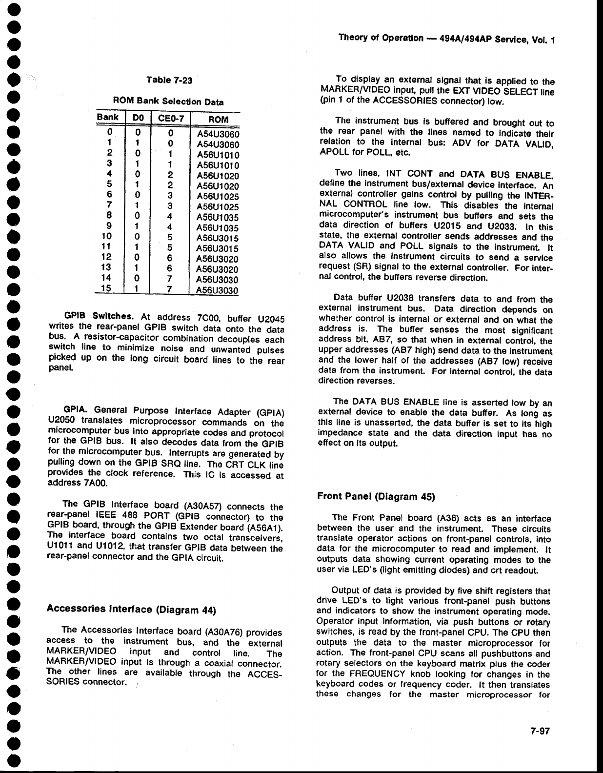
o
o
o
o
o
o
o
o
o
a
a
o
o
o
o
o
o
a
o
,
o
o
o
o
o
t
o
o
I
o
a
o
I
o
o
a
a
I
o
o
o
a
o
o
Accessories lnterface (Diagram
44)
The Accessories
lnterface
board
(A90A76)
provides
access to the instrument bus, and the external
MARKER/VIDEO
input and controt tine. The
MARKERIVIDEO
input is through
a coaxial
connector.
The other lines are availabls
through the ACCES_
SORIES connector.
Theory
of Operatlon
- 4g4ful494Ap
Servlce,
Vol.
1
Iq display
an Externat
signal
that is applied
to the
MARKEF/V|DEO
input,
putt
the
EXT
vtDEo SEtect tine
(pin
1 of the
ACCESSORTES
connector)
tow.
The instrument
bus is buffered and brought
out
to
the rear panel
with the lines named
to indacate
their
relation
to the internat
bus: ADV for DATA VALID.
APOLL
for POLL.
etc.
Two lines, tNT CONT and DATA BUS ENABLE.
define
th€ instrument
bus/external
device
lnterface.
An
external
controller gains
control
by pulling
the INTER-
NAL CONTROL
line tow. This disabtes
th€ internal
microcomputer's
instrument
bus buffers
and sets th€
data direction
of buffers
U201S and U2033. In this
state,
the external
controller
sends
addresses
and
the
DATA
VALID
and pOLL signals
to the instrurnent.
lt
also allows
th€ instrument
circuits
to s€nd a service
request
(SR)
signal
to the external
controller.
For inter-
nal control,
the
buffers reverse
direction.
Data
buffer
U2038
transfers
data to and from the
external
instrument
bus. Data direction
depends
on
whether
control
is internal
or external
and
on what
the
address is. The buffer senses the most significant
address
bit, AB7,
so that when
in external
control.
the
upper
addresses
(AB7
high)
send
data to the instrument
and th€ lower
half of the addresses (AB7
low)
receive
data
from
the instrument.
For internal
control,
thE
data
direction
reverses.
The DATA
BUS ENABLE
line
is asserted
low
by an
external
device
to €nable
the data buffer. As long as
this line
i$ unasserted,
the
data buffer
is set to its high
impedance
state and the data dirEction
inout
has no
effect
on
its
output.
Front Panel (Diagram 45)
The Front Panel board (A38) acts as an interface
between
the user and the instrument.
These circuits
translate operator
actions
on front-panel
controls,
into
data
for the microcomputer
to read
and implement.
lt
outputs
data showing
current
operating
modes
to the
user
via
LED's
(light
emitting
diodes) and crt readout.
Output
of data is provided
by five
shift registers
that
drive LED'S
to light various
front-panel push buttons
and indicators
to show
the instrument
operating
mode.
Operator
input information,
via push buttons or rotary
switches,
is read
by
the front-panet
CpU. The
CpU then
outputs the data to the master microprocessor
for
action. Th€ front-panel
CPU
scans
all pushbuttons
and
rotary selectors
on the keyboard
matrix
plus
the
coder
for the FREQUENCY
knob looking
for changes in the
keyboard codes
or frequency coder. lt then
translates
these changes for the master microprocessor for
Tabte
7-23
ROM
Bank
Selection
Data
Bank DO cE0-7 ROM
0
1
2
3
4
5
6
7
I
9
10
11
12
13
14
15
0
1
o
1
0
1
0
1
0
1
0
1
0
1
0
1
0
0
1
1
2
2
3
3
4
4
5
5
6
6
7
7
454U3060
454U3060
456U1010
456U1010
456Ur020
456U1020
456U1025
456U1025
456U1035
As6Ul
035
456U301
5
A56U301
5
456U3020
456U3020
A56U3030
456U3030
GPIB Swltches. At address 7C00, buffe r u2O4E
writes
the rear-panel
GplB switch
data onto the data
bus.
.A.resistor-capacitor
combination
decouples
each
switch line to minimize
noise and unwanted
pulses
picked
up on the long circuit board
lines
to th6 rear
panel.
GPIA. Generat
purpose Interface
Adapter
(GplA)
U2050 translates microprocessor
commands
on the
microcomputer
bus into appropriate
codEs
and protocol
for the GPIB
bus. lt also
decodes
data
from
the GplB
for the
microcomputer
bus._ lnterrupts
are
generated
by
pulling
down
on the
GptB SRe line. fne Cnf CLK
tini
provides
the clock reference. This lC is accessed
at
address
7A00.
The GPIB Interface
board (A30A57)
connects
the
r€ar-panel
IEEE 488 PORT (GptB connector)
to the
G.PIB.
board,
through
the GptB
Extender
UoarO
(nSOet;.
The interface
board contains
two octal transceiveri,
Ul011 and
U1012,
that
transfer
GptB
data
between
the
rear-panel
connector
and
the
GplA circuit.
7-97
Theory of Operaton - 4g4[l4g4Ap Servtce,
Vot. 1
appropriate
action. Th€
following
is a description
of the
hardware and a brief
description
of the software
used
bythe front
panel
CPU.
Potentiometers.
The following controls or adjust-
ments
generate
analog
signals
used
by other
functions
of the instrument. These controls are non-
programmable.
INTENSITY
is an input
to th€ Z-Axis/RF
Interface
board
to control
trace brightness.
PEAK/AVERAGE
is a digitat storage input that
causes
signals
to be either peak detected
above
or
averaged
below
a displayed
cursor
lane
that
tracks
this
control.
MANUAL
SCAN
sweeps
the spectrum
or display in
manual
sweep
mode.
POSITION centers the horizontal and vertical
deflection
on
the crt.
LOG/AMPL
CAL varies
the video signal
level
prior
to the Video Processor
board and adjusts
10
MHz lF
gain
to calibrate
the
log
display.
OuFut Mode Shift Registers
and LED'. As previ-
ously
described,
LEDs
mounted
behind
a pushbutton
or
below front-panel
labels
indicate
the mod€ of operation.
Some versions
of the
spectrum
analyzer
may
not
use
all
indicators; for example,
the non-programmable
versions
do not have a RESET
TO
LOCAL
button,
The LEDs are driven by shift registers (U5O4S,
U6081, U6028, U6045. and U1049) that reside at
address
74
(hex)
on
the instrument
bus. The
shift
regis-
t€rs that drive
the LEDs
are
reloaded
each
time
a LED
changes
state. The master microprocessor
changes
the appropriate
bit in the LED code then reloads
all
registers. The shift register U60gl that drives the
GRAT ILLUM
LED also controls
the voltage
regulator
U6090,
which provides
power
for the graiicule-lights,
DSl0t1
and DSl013.
Proeessor.
The
CPU is an
874i self-contained
g-bit
microprocessor
with on-chip
EPROM
and RAM. Refer
to Intel
UPI Users
manual
for a complete
description
of
the this microprocessor (lntel
8741).
The
lC has
a self-contained
clock
and
a timer. The
clock uses a 6 MHz crystal,
y3030, as the resonator.
The timer functions
either
as a programmable
timer
or
counter.
7-98
The CPU
has
two input/output
ports. Port
plGplT
is input
only
and
P20-P27
in an input/output
port. Each
port is 8-bits wide. In addition, the CPU has an 8-bit
data port (D0-D7)
called
the output buffer, which
tatks
to
the master
microprocessor. In this application
all data
is output only with U4030 being a buffer between
lhe
GPU
and the instrurnent
bus. Infoffnation
that the cPU
wishes
to relay
to the master microprocessor,
is loaded
into
a latch
connected
to the output
buffer
U4030. The
master microprocessor
accesses
the CPU by pulling
address F4, out of decoder U6024, low to activate
the
output
bufier and enable
U4030
so data
is passed
onto
the instrument
bus.
The CPU is reset by the master
microprocessor.
When DB3 is selected for more
than 10 ms (same
as
writing 08 at address 74)
C1016 charges
and U1024A
output
resets
the CPU.
Scanning the Keyboard. The front-panel
keyboard
is arranged in a matrix of 4 rows of I columns
and
6
rows of 7 columns
(see
Table
7-24). The
RESOLUTION
BANDWTDTH, SPAN/D|V, T|ME/D|V, MIN RF
ATTEN
dB, and REFERENCE
LEVEL selectors are
rotary switches where
each contact occupies
a position
in the keyboard switch matrix. The TIME/D|V and
MIN
RF ATTEN a(e position dependent. The master
microprocessor
notes
the
current s€tting of these
selec-
tors by noting which contacts are closed.
When a
change is made
the
master
microprocessor
notes which
direction the selector was moved
by noting
the relative
position
of the current contact
closure
with
the
previous
setting. Pull
up resistors, within
R2041
plus
R2044, on
each column of the row currently
being
read,
will pull
that column high
if the switch is open. The
basic
algo-
rithm
of scanning is to pull
one row at a time
down
and
note which columns have
a 1 or 0. Port one.
Pl
0-P17
(pins 27€4), read the columns. Part of port two (pins
21-241 are responsible
for activating
the
rows. Basically
the process
consist of pulling
one row at a time down
to E logic 0 and then reading all the columns. lt a
switch contact
is open
it reads
a "1
" and if it is closed it
reads
a "0'.
Since
there are 10 rows to scan
and only 4 pins
(P2O-P231available
at the number
2 port,
the
output
is
multiplexed
through U4021
and U5021.
These lC's are
open collector output, TTL compatible
multiplexers.
They
decode data
out of P2O, P21, P22, and P23
(pins
21-241
and their output pulls the appropriate row of
keys
down.
Due to the characteristics
of the switch
matrix. if
two keys,
in any
row or column are closed, and
a third
is closed so three corners of a rectangle are esta-
blished in the key matrix,
the CPU will see a phantom
closure at the fourth corner. For example;
if Y6/X3,
Y6/X7
are
closed, and
then
Y3lX7
is closed,
the
CPU
o
o
o
o
o
o
o
a
o
a
I
o
t
)
t
o
o
o
o
o
o
O
o
o
I
I
o
o
a
o
o
o
a
o
O
I
a
a
I
o
o
a
o
o
O
o
o
o
o
o
o
o
o
o
o
a
o
o
o
o
o
o
o
o
O
o
o
o
o
O
)
o
a
o
o
o
t
o
o
o
o
o
O
o
o
o
o
o
will see
a phantom
closure
at y2lxg as
it scans
the
key
matrix. To suppress
these piantom key closures,
diodes have
been added
in series
with the RESOLU-
noN BANDWTDTH,
MtN RF ATTEN,
SpAN/D|V,
and
gerta]l other
keys in column
6 and
7 of the k'ey
matrix.
In addition,
an €rror
detection
algorithm
is used
in the
CPU
to eliminate
additional
ptraniom
key
closures
that
might occur.
_ scanntng the FREoUENCy
controt coder. The
FREQUENCy
control
contains
a pair
of phototransistors
that
outpul
a gray
code
through
Ut024Ei
and
U1024C
to
P27.
and p26 (pins
37 and
36; ot the CpU. This gray
code
signifies
the direction
the
control
is
turned.
Ou-rini
a scan
cycle,
the GpU looks
at th€ status
of the FRE-
QUENCY
control
code
and if it detEcts
a change,
the
CPU
performs
a shift
and
exclusive,OR
operation
which
derives
the correct
code
to output
ouer
ihe instrument
bus
to the master
processor
to tell
it which
direction
to
tune
the center
frequency.
Outputting
the Correct Code. The remaining
two
bits.out of port 2 (pZ4
and p25)
drive
the appropriate
hardware
and initiate
an SRe on the instrument
bus.
When th€ SER REe line is pulled
down,
the master
microprocessor
will service
either
the keyboard
or th€
fre-quency
coder. The
front
panet
CpU
(Uir0gg)
initiates
a SRQ
by putting
down
p24 or p2S. A tow
out ot pZ4
(pin 35) wilt initiate a keyboard
SRe. The master
microprocessor
will
now
service
the request
by reading
the keyboard
data in output
buffer
U4$b. A low out
ol
P25 (pin
36) initiates
a FREQUENCy
controt
SRe and
causes the master microprocessor
to service the
request
by reading
the frequency
code in the output
buffer.
A low
out
ot p24
is inverted
by U2020C
so it clocks
the flip-flop
Ug013B. The resultint low on the e(bar)
output puils the sER REQ tine down. (Refer
to thg
instrument
bus POLL sequence
described
under the
master microprocessor
description
for the service
request sequence.)
The master microprocessor
now
raises both the POLL tine and ABZ. This is gated
through
u4014A
as
a low
to DBo
on
the instrument
bus.
The master
microprocessor
reads
the bus
and sees
a
low on DB0. This indicates
that a keyboard
interrupt
has
occurred
and
it must
read
the
new
kevboard
code.
The master
proeessor
first clears
the interrupt
by pul-
ling
AB7
and
then
the
POLL
tine
tow. DBO
now
goes
high. The master
microprocessor
now writes
a 0 to
DBo,
the same
as it read,
and
raises
the
pOLL
line.
This clocks
U3013A
and
resets
Ug0138
which
removes
the SRQ(bar).
The
instrument
processor
now
reads
the
data in the output
buffer,
U4Og0,
at address
F4. The
front panel
CPU now recognizes
that its output
buffer
has
been read
and
it resets
p24to
a 1. lt is
now ready
Theory
of Operation
- 4g4[l4g4Ap Service,
Vol. 1
for
another
cycle.
A similar
process
occurs
when
p25 (pin
36) of the
CPU
is p_u!l9d
low by a FREQUENCy
coder
inteirupt.
A
!9y on P25 is propagated
through
UZ02OB,
U20t3A,
U20138, and
U4014C;
onty
this
time
DB3
is invotved
in
the pofl. U2020A and U40148
decode a low on AB7
and
high on POLL
tine
to ctock
U20t3A and
3013A.
soltware. The algorithm
that the cpu follows con_
sists
of a main
scan
routine,
which
is an endless
toop,
and four subroutines
that can be called. One su6_
routine
runs
the on-chip
timer
that
is used
to debounce
the keys, Another
subroutine
reads
the frequency
knob
coder and derives th€ proper code to output io tne
master
processor.
The
third
subroutine
reads
the key_
board and stores the address
of all keys that weie
closed. The fourth subroutine
looks at the keycode
from the key addresses
that were
stored,
and
outputs
the key codes andlor frequency
code for the master
processor. There are also a number
of checks
and
tests
that
have
to be
done in
each
routine in addition
to
the obvious
tasks.
Main Scan Routine. There are two types of scan;
the
first
is made
after
a reset.
the second
type
consists
of the following
scans;
the keyboard,
frequency
coder,
and
the output
data. During
the first
scan,
data in the
GPU is initialized.
The
CpU reserves
part
of its RAM
to
store
and remember
all key and
frequency
knob
coder
settings.
During all scans,
the
CpU reads
the
frequency
code and each row of keys on the keyboard.
lt com-
pares
what it read
to that stored
in RAM
and
if there
is
a difference,
the CPU
calls
the appropriate
subroutine
for either
the keyboard
or the frequency coder knob.
After a complete scan,
the CPU checks
to see if new
information
needs to be output to the instrument
pro-
cessor, lf it does
the CPU calls
up the
output
subrou-
tine.
Prior
to the first scan,
after
reset.
the CpU puts
all
1's (highs) into its keyboard memory. This
corresponds
to op€n
keys.
On the ftrst
scan,
the CpU
will note five apparent
closures
due to the TIME/DIV,
MtN RF ATTEN, SPAN/D|V, RESOLUTION
BANDWIDTH,
and REFERENCE
LEVEL selectors.
These
closures are
noted and
output
to the master
pro-
cessor. Because
the master
processor
memory
knows
the
position
of each
selector
to close
a key,
the
proces-
sor calls these the power-up
settings. When
a front
panel
knob changes
position
the master
processor
can
determine
which
direction
the
knob
changed and what
it
must
do to respond
to the change. A complete
scan,
without
detecting any
key
closures
takes
about
800 us,
7-99
Theory
of Operaton - 494[l4g4Ap Service,
Vot.
1
Keyboard Check Subroutine.
This subroutine
is
called
when
the main
scan
routine
detects
a change
in
the keyboard
matrix
which occurs
when
a key
opens
or
closes. A key opening
usually
signifies
that an action
has been
completed,
whereas
a closure
indicates
that
an operation
or action
is requested
by the user;
there-
fore,
the two are treated
differently
by the
cpu.
Because
mechanical
keys
tend
to bounce
when
they
open
or close,
the subroutine
must
debounce
each
key
change.
To debounce,
the
subroutine
calls
up the
timel
subroutine.
This sets a number
into the internal
timer
and starts
it running.
When
the
timer has
timed out,
in
about a millisecond,
the keyboard subroutine
again
scans
the row and compares
this scan with the scan
before
the
debounce
check. lf the scan
does
not com_
pare, the routine assumes
the key change was a
bounce or glitch,
and
it returns
to the main
scan
routine.
lf it does compare,
the routine
then recognizes
that a
key state
has changed
The routine
then checks
to see if this is the first
scan
that looked
for a key
change
after
it has outputted
previous
information
to the master
processor. lf it is
the first pass
then the routine
causes
the CpU to re_
scan
the
full
keyboard
matrix
to ensure
that
th€re
is not
a phantom
key closure. lf this is the second
or subse-
quent
pass
and
an actual
key
change has
occurred,
the
routine
then notes
if the key
change
was an opening
or
closure.
lf the change was an opening
the CpU memory
is
updated
to the fact that the key is open. lf a closure
has occurred,
the routine
will then check the column
that
has
the
closure
and
output
a new key
address
onto
the output stack. This addr€ss
consists
of the key's
row and colsmn
location.
After outputting
the address,
the subroutine
returns
to scanning
the remainder
of the
keyboard
matrix.
Frequency
Coder
Subroutine
Check. This subrou-
tine is called when the main scan routine detects
a
change
in the frequency
coder switch. Like the key-
board subroutine,
this routine
also debounces
the fre-
quency
coder
switch
after
every change
to ensure
that
the switch
code has
changed:
lf a real
change
is noted,
the routine
proceeds
to determine
the direction
of the
change.
The frequency
knob
outputs
a two-bit
code
with only
one bit at a time changing as the
control
is rotated. The
direction the knob is rotated is determined
by the
pro-
perty
of a gray
code,
generated
by an exclusive-OR
log-
ical operation
within the CPU. The previous
state
of
one bit is compared
with
the current
state of the other
bit. Down {counterclockwise
rotation)
yields unequal
inputs, whila
up (clockwise
rotation
) yields
the oppo-
site. The bit that indicates
direction
is inserted
as the
MSB for the frequency
coder byte. This byte is then
loaded into the output stack. The subroutine
then
returns
to the
main
scan
routine.
Output Subroutine. After each scani the CPU
checks its output register
to see if any information
needs
to be output. lf it needs to be
output,
th€
output
subroutine is called
up; if not,
another
scan is start€d.
The output subroutine
checks a number
of things
before
it outputs any
information
to the
output
register.
lt first
determines if the
CPU
is on its first or initial scan
after
a
reset. The first
scan will contain more
than
one closure.
All of these
closures
must be
output
before
it continues.
On
all scans
that
follow,
the
routine looks
for more
than
one closure
by checking
the numbEr
of entries into
the
output stack. lf more than one closure has been
entered,
the output
routine aborts. This eliminates
out-
putting
phantom
key
closures.
The routine
is now ready to output
information.
lt
pulls
a key address from
the
output stack
and
looks
up
the
code from
a look-up
table
in
RoM. This key code
is
loaded into the data port or output buffer. The
appropriate
poft P24 or P25
( pins
35 & 36)
is pulled
low. The routine continuously
reads the frequency
coder
and
updates
its memory
while it is waiting
for
the
rnaster
processor
to read
the data in the output
buffer.
Once the data has been
read, P24
or P25 goes
high
and the subroutine starts
to check
the output stack
for
more key closures. When
the output stack is empty,
the first scan
flag is rescinded and
the cPU returns
to
its main scanning routine.
a
o
o
O
o
o
o
o
o
o
o
o
o
o
o
a
o
o
O
o
o
o
o
o
o
o
e
o
o
o
o
O
o
o
o
o
o
O
o
o
o
o
o
o
7-100
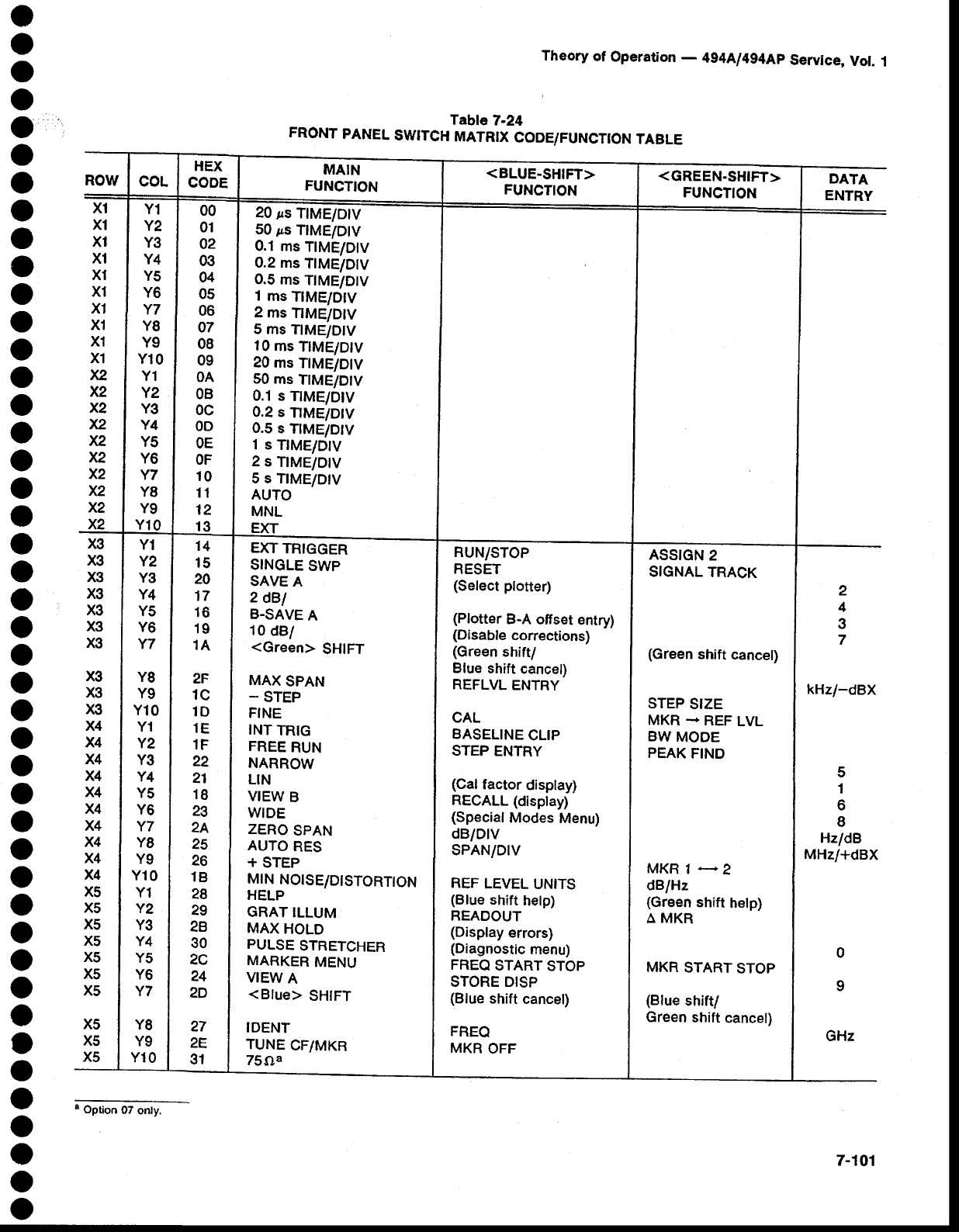
Theory
of Operation
- 494A1494Ap
Sewice, Vot.
.t
DATA
ENTRY
kHz/-dBX
5
1
6
I
HzldB
MHz/+dBX
ROW
o
o
o
o
o
o
o
o
o
o
o
o
o
o
o
o
o
o
o
o
o
o
o
o
o
o
o
o
o
o
o
o
o
o
o
o
a
o
o
o
o
o
o
o
2
4
3
7
X1
X1
X1
x1
X1
X1
X1
xl
x1
X1
,<2
,<2
x2
x2
><2
x2
x2
)<2
x2
x3
x3
x3
x3
x3
x3
X3
x3
X3
x3
x4
x4
X4
x4
x4
x4
X4
x4
x4
x4
X5
X5
x5
X5
X5
x5
x5
X5
x5
X5
Table
7-24
FRONT
PANEL
SWTTCH
MATRTX
CODE/FUNCT|ON
TABLE
Y1
Y2
Y3
Y4
Y5
Y6
Y7
Y8
Y9
Yl0
Y1
Y2
Y3
Y4
Y5
Y6
Y7
Y8
Y9
00
01
02
03
04
05
06
07
08
09
OA
OB
0c
OD
OE
OF
10
11
12
13
20
ps
TIME/DIV
50
ps
TIME/DIV
0.1
ms
TIME/D|V
0.2
ms
TIME/DIV
0.5
ms
TtME/D|V
1 ms
TIME/D|V
2 ms
T|ME/D|V
5 ms TIMEID|V
10
ms
TIME/D|V
20
ms
TIMEID|V
50
ms
TIME/DIV
0.1 s TIME/D|V
0.2 s TIME/DIV
0.5
s TIME/DIV
1 s nME/DtV
2 s TIME/O|V
5 s TIME/D|V
AUTO
MNL
EXT
Y1
Y2
Y3
Y4
Y5
Y6
Y7
Y8
Y9
Yl0
Y1
Y2
Y3
Y4
Y5
Y6
Y7
Y8
Y9
Y10
Y1
Y2
Y3
Y4
Y5
Y6
Y7
Y8
Y9
Yl0
2F
1C
1D
1E
1F
u
21
18
29
2A
25
26
1B
28
29
28
30
2C
24
20
27
2E
31
EXT
TRIGGER
SINGLE
SWP
SAVE
A
2 dBl
B-SAVE
A
10
dB/
<Green>
SHIFT
MAX
SPAN
- STEP
FINE
INT
TRIG
FREE
RUN
NARROW
LIN
VIEW
B
WIDE
ZERO
SPAN
AUTO
RES
+ STEP
MrN
NOTSE/DISTORT|ON
HELP
GRAT
ILLUM
MAX
HOLD
PULSE
STRETCHER
MARKER
MENU
VIEW
A
<Blue>
SHTFT
IDENT
TUNE
CF/MKR
75f,}a
RUN/STOP
RESET
(Select
plotter)
(Plotter
B-A
offset entry)
(Disable
corrections)
(Green
shift/
Blue
shift
cancel)
REFLVL
ENTRY
CAL
BASELINE
CLIP
STEP
ENTRY
(Cal
factor
display)
RECALL (display)
(Special
Modes
Menu)
dB/Dtv
SPANiDTV
REF
LEVEL
UNITS
(Blue
shift
help)
READOUT
(Display
errors)
(Diagnostic
menu)
FREQ
START
STOP
STORE DISP
(Blue
shift
cancel)
FREQ
MKR
OFF
ASSIGN
2
SIGNAL
TRACK
(Green
shift
cancel)
STEP
SIZE
MKR
* REF
LVL
BW
MODE
PEAK
FIND
MKR
1
+2
dBlHz
(Green
shift
hetp)
A MKR
MKR
START
STOP
(Blue
shift/
Green shift
cancel)
e Option 07 onty.
7-101
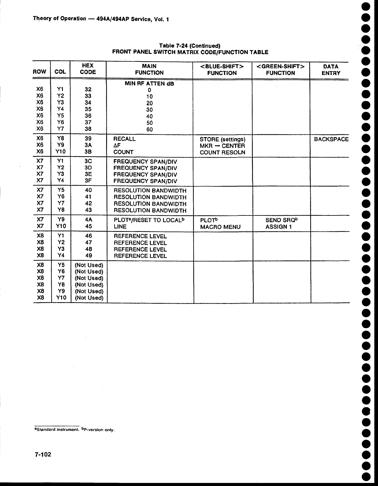
ROW coL HEX
CODE MAIN
FUNCTION <BLUE.SHIFT>
FUNCTION <GREEN.SHIFT>
FUNCTION DATA
ENTRY
X6
X6
X6
X6
X6
X6
X6
Y1
Y2
Y3
Y4
Y5
Y6
Y7
32
33
34
35
36
37
38
MIN RF ATTEN
dB
0
10
20
30
40
50
60
X6
X6
x6
Y8
Y9
Yl0
39
3A
3B
RECALL
AF
COUNT
STORE
(settings)
MKR
- CENTER
COUNT RESOLN
BACKSPACE
x7
x7
x7
x7
Y1
Y2
Y3
Y4
3C
3D
3E
3F
FREQUENCY
SPAN/D|V
FREOUENCY
SPAN/D|V
FREOUENCY
SPAN/D|V
FREOUENCY
SPAN/DIV
x7
x7
x7
x7
Y5
Y6
Y7
Y8
40
41
42
43
RESOLUTION
BANDWIDTH
RESOLUTION
BANDWIDTH
RESOLUTION
BANDWIDTH
RESOLUTION
BANDWIDTH
x7
K7 Y9
Y10 4A
45 PLOTa/RESET
TO LOCALb
LINE PLOTb
MACRO
MENU SEND SROb
ASSIGN
1
x8
X8
x8
x8
Y1
Y2
Y3
Y4
46
47
48
49
REFERENCE
LEVEL
REFERENCE
LEVEL
REFERENCE
LEVEL
REFERENCE
LEVEL
x8
x8
x8
x8
x8
x8
Y5
Y6
Y7
Y8
Y9
Yl0
(Not
Used)
(Not
Usecl)
(Not
Used)
(Not
Used)
(Not
Used)
(Not
Used)
Theory
of Operatlon
- 494A1494Ap
Service,
Vol.
1
astandard instrument. bP-version only.
7-102
Table 7-24
(Continued)
FRONT
PANEL
SWTTCH
MATRTX
CODE/FUNCT|ON
TABLE
o
o
o
o
o
o
o
o
o
o
o
o
o
o
o
o
o
o
O
o
o
o
o
o
o
O
o
o
o
o
o
o
o
o
o
o
o
a
o
o
o
o
o
o
Theory
of Operation
- 4g4A/494Ap
Servlce,
Vol. 1
o
o
O
o
o
o
o
o
o
O
o
o
o
o
o
o
o
o
o
O
o
o
o
o
o
o
o
o
o
o
a
o
O
o
o
o
o
o
o
o
o
o
o
o
POWER
SUppLy
(Diagram
10)
The Main power
Supply
furnishes
all the regulated
voltages
for the spectrum
analyzer,
exc€pt
the crt high-
voltage
:uppty. The high-efficiency
desiin of the Main
Power Supply reduces total weight ind conserves
en_ergy.
The power
supply
circuits
lre divided
into
th€
primary
circuits
and the iecondary
and fan drive
cir-
cuits.
primary
Circuits
(Diagram
46)
. .ft" power
supply
primary
circuits
consist
of the
fol_
rowing:
the rine
input
circuit,
wnicn
rectifies
and firters
the incoming
line
voltage;
and
the inverter,
which
drives
the
primary
of the
power
transformer.
Line Input Circuits
_^ Power
is applied
through
tine
filter
FLg0l
, line
Fuse
F301,
. and through FLgb2 (for additional normal
mode/common
mode EMt fittering)
to POWER
switch
5300. The
power
is
then
sent
thro-ugh
line
s€lector
con-
nector J1091. The line filter plevents power-line
interference
from entering
the
power
supply,
and
it also
prevents
internally-generated
signals
from
radiating
out
the
power
cord.
Line
selector
switch
S302
allows
instrument
opera_
tion
trom
€ither
a lSV nominal
or 230V nominal
line
voltage
sourcg. With
S3O2
is in
the
115
V position,
pins
1 and
2 of p1091
are
connected
to the
input power,
and
rectifi€rs
CR3096
and.
CR4094
operate'in ionjunction
with
energy
storage
filter
capacitors
C6101
and
C6111
as
a full-wave
doubleq
thus,
the
voltage
across
the
two
9lqacllol: is the peak_to_peak
vatue
oJ
the
line
vottage.
With
S302 in the 290
V position,
pins
2 and
3 of p1091
are
connected
to the
input powerand
CR3096,
CR4O95,
CR3098,
and CR4094
operate
as a bridge
rectifier.
As
a-
result,
the output
voltage
appliecl
to the inverter
is
about
the same
for 1lS V or 23b-V
operation.
Because
G6011
and
C610.t
discharge
very
slowly,
hazardous
potentials
exist
wiihin
tne
power
supply
for several
minutes
after
the
POWER
switch
is turned
off. A relaxation
oscillator
formed by C51 lg, R5l
11, and
DS51
12,
indicates
the presence
of voltages
in the circuit until
the potential
across
ihe
filtor
capacitors
is below
g0
V.
Thermistors
RT209g
and
RT2097
limit
current
surge
at turn on. After
the instrument
warms
up,
the
current
demand
drops. The
increase
in
temperature
decreases
the resistance
value
of the thermistors
so they have
minimum
affect
on
the circuit.
Thermal
cutout
switch
S2109
opens
if thE interior
of
the instrurnent
reaches
109"C
to prevent
overheating
in
case
the cooling
fan
fails.
E1094 and E2095 are surge voltage
protectors.
When
the line selector
switch
is in the 115
V position,
only
E1094
is connected
across
the
line
input.
it a peak
voltage surge in €xcess of 230
V occuis across the
input,
or if the
instrument
is accidentally
connected
to a
230
V source, E1094
will break down and demand
enough
current
to open
the line
fuse. When
the
instru-
ment
is operated
with
the line
selector
at 230v,
E1094
and
E2095
operate
in series
to protect
the
input
against
line
surges
of approximately
460
V peak.
, The voltage for the line trigger is taken across
CR3096. This 48
Hz to 440
Hz vottage
drives
optical
isolator
U5043. The
pulsating
5 V output
is ac coupled,
then sent both to the Sw€ep
circuit
to provide
instru,
ment
triggering
at ths line
frequencios
and
to th€
Z-Axis
board
for the
Power-Fail
Detector
circuit.
Inverter Circuit
The inverter
consists
of a multivibrator
that pro_
duces
a rectangular
shaped
signal
to drive
the ramp
generator
and
th€ inverter
logic
circuits.
The
ramp
gen-
erator produces a low-level sawtooth ramp that is
applied
to the primary
regulator
circuit. The inverter
logic
circuits
control
the
duty
cycle
of the inverter
driver
and the inverter
output stage. The primary
regulator
circuit
compares
the +l 7 V supply
output
with
a refer-
ence voltag€,
then
gates
the inverter
logic
circuits
off
and on to control the inverter duty cycle and the
effective
primary voltage. The inverter
driver stage
amplifies
the signal
from the inverter
logie
circuit
and
drives
the output
stage, The output
stage
consists
of
two power
switching
transistors
that drive the
primary
of main power
transformer
T4021. The primary
ovei-
current
sense
and soft
start
circuits
add
protection.
Multivibrator.
U6059, a low-power
S55 tirner,
is a
multivibrator
that operates
at approximately
66 kHz
and
90-7-"-
duty cycle. Oscillator
frequency
is adjusted
by
R6061.
The rectangutar-shaped
output
signat
is appliei
through
R6052
to the
primary
of T6044
in
the
ramp
gen-
erator and
atso
directty
to u6053,
u6063A,
u60638, and
u6069.
7-103
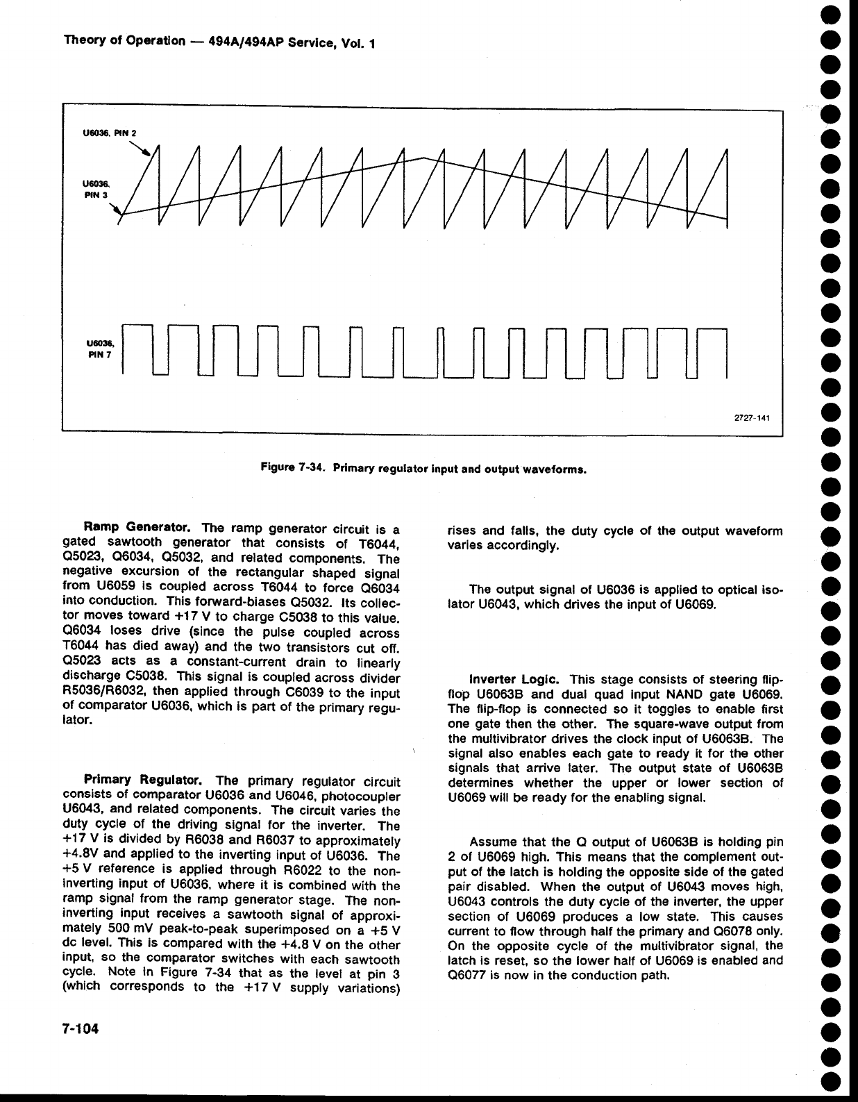
Theory
of Operaton - 494A/494Ap
Servtce,
Vot.
1
u$36. PrN
2
u603A
PIN 3
u6036,
P|l{ 7
Figure
7-34, Primary
.egutator
Input
and output waveforms.
a
o
o
O
o
o
o
a
o
o
o
o
o
o
o
a
o
o
o
o
o
o
o
o
o
o
o
O
o
o
a
o
o
o
o
o
O
o
o
o
o
o
a
o
Ramp Generator.
The ramp generator
circuit is a
gated sawtooth generator that consists of T6044.
Q5023, Q6034,
Q5032,
and related
components.
The
negative
excursion
of the rectangular
shaped signal
from U6059 is coupled across T6044 to force e6094
into conduction.
This
foruvard-biases
e5032. lts coll€c-
tor moves
toward +17
V to charge
Csogg
to this
value.
06034 loses drive (since the pulse coupled across
T6044
has died away)
and the two transistors
cut off.
05023 acts as a constant-cunent
drain to linearly
discharge
C5038.
This
signal
is coupled
across
divider
R5036/R6032,
then apptied
through
C6Og9
to the input
of comparator
U6036,
which
is part
of the
primary
regu-
lator.
Prlmary Regulator. The primary regulator
circuit
consists
of comparator
U6036
and
U6046,
photocoupler
U6043,
and related
components.
The circuit
varies
the
duty cycle of the driving
signal for the inverter. The
+17
y is divided
by R6038
and R6097
to approximatety
+4.8V
and apptied
to the inverting
input
of U6036.
Thi
+5 V reference
is apptied
through R6022
to the non-
inverting input
of u6036,
where
it is combined
with the
ramp signal
from the ramp generator
stage. The non-
inverting
input receives
a sawtooth
signal
of approxi-
mately
500 mV peak-to-peak
superimposed
on a +S
V
dc level.
This
is compared
with the +4.9
V on the other
input, so the comparator
switches
with each
sawtooth
cycle. Note in Figure
7-34 that as the level at pin g
(which corresponds
to the +I7 V supply variations)
7-104
rises
and falls, the duty cyele
of th€ output waveform
varies accordingly.
The output
signal of U6036
is applied
to optical
iso-
lator
u6043, which
drives the input
of u6069,
lnverter
Loglc. This stage consists of steering flip-
flop U6063B
and dual quad input
NAND
gate U6069.
The flip-flop
is connected so it toggl€s
to enable first
one gate
then the other. The sguare-wavg
output
from
the multivibrator
drives
the
clock
input
of U60638. The
signal also enables
each
gate
to ready it for the other
signals
that arrive later. The output
state of U60638
determines whether the upper or lower section of
U6069
will
be
ready for the
enabling signal.
Assume
that the Q output
of U60638
is holding
pin
2 of U6069 high. This means
that the
complement out-
put
of the
latch is holding
the
opposite
side of the
gated
pair disabled.
When the output of U6043
moves high,
U6043
controls
the duty
cycle of the
inverter, the upper
section
of U6069
produces
a low state. This causes
current
to flow
through
half
the
primary
and Q6078
only.
On the opposite cycle of the multivibrator
signal, the
latch is reset, so the lower half of U6069
is enabled
and
Q6077 is now in
the
conduction
path.
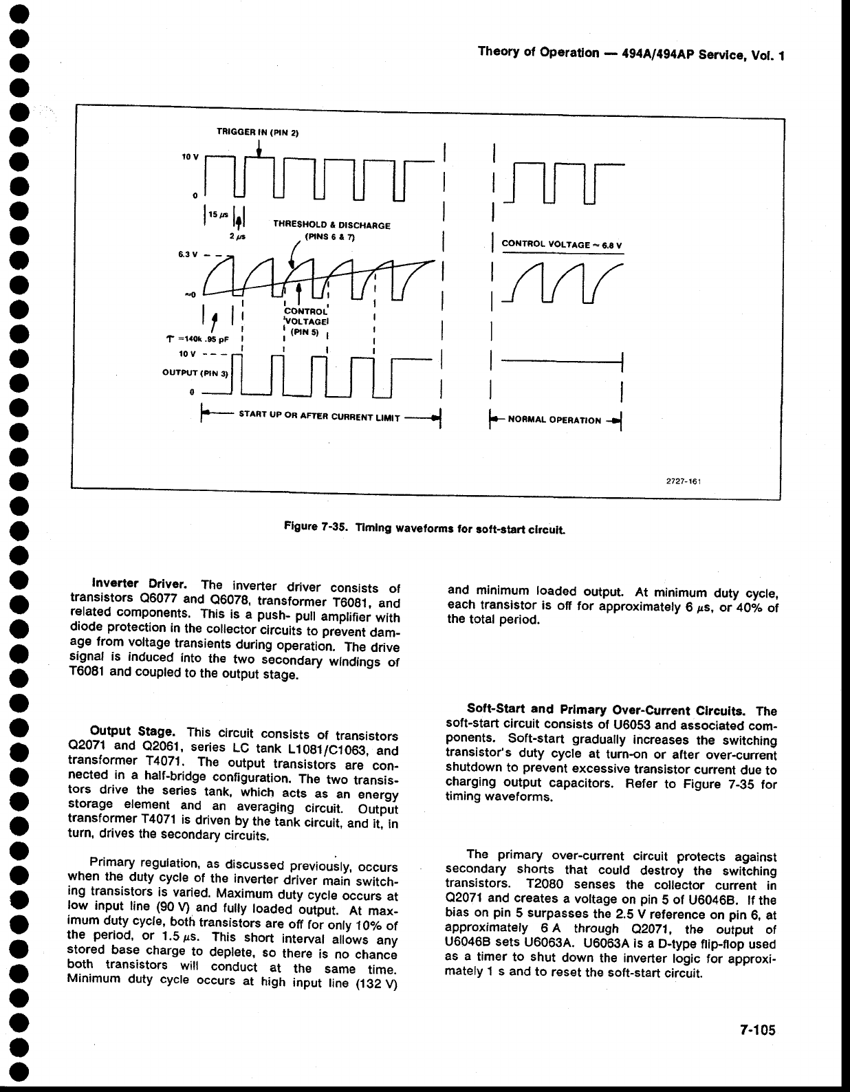
O
o
o
o
o
o
o
o
o
o
o
o
o
o
o
o
o
o
o
a
o
o
o
o
o
o
o
o
o
o
a
O
o
o
o
o
o
a
o
o
o
o
O
o
Theory
of Operation
- 494[l4g4Ap Servlce,
Vot.
1
Flgure
7-35. Tirning
waveforms
for soft-start
clrcuit
Inverter Driver. The inverter driver consists of
transistors
Q6072
and
e6079,
transformer
T60g1,
and
related
components.
This
is a push-
pull
amplifier
with
diode
protection
in
the collector
circuits
to pr€vent
dam,
age
frorn
voltage
transients
during
operation.
The
drive
signal
is induced
into.the two slcondary wlndings
of
T6081
and
coupted
to the
output
stage.
^ 9utput Stage. This circuit
consists
of transistors
Q.2071
and Q2061,
series
LG tank L10g1/C1063,
and
transformer
T4071
. The output transistors
are con-
nected
in a half-bridge
configuration.
The two transis-
tors drive the series
tank, which acts as an energy
storage element and.
.
an averaging circuit. Outp-ul
transfonner
T4071
is driven
by
tne
tanf circuit,
anct
it, in
turn,
drives
the
secondary
circuits.
Primary
regulation,-as
discussed
previously,
occurs
when
the duty cycle
of the inverter
driver
main
switch_
ing
transistors
is varied.
Maximum
duty
cycle
occurs
at
low input
line (90
V) and
fulty
toaded
output. At max-
imum
duty cycle,
both
transistbrs
are
off
for
only
1Ao/o of
the period,
or l.Sps. This short interval
allbws any
stored
base
charge
to deplete,
so there
is no chance
both transistors will conduct at the same time.
Minimum
duty cycte
occurs
at high
input
tine (132
V)
and minimum
loaded
output. At minimum
duty cycle,
each
transistor
is off for approximately
6 ps,
or 4O;/o
ot
the
total
period.
Soft'Start and Prlmary Over-Current
Clrcuits. The
soft-start
circuit consists
of U6053 and
associated
com-
ponents. Soft-start
gradually
increases
the switching
transistofs duty cycle at turn-on
or after over-current
shutdown
to prevent
excessive
translstor current
due to
charging
output capacitors. R€fer
to Figure
7-35 for
timing waveforms.
The primary over-current
circuit protects against
secondary
shorts that could destroy the switching
transistors. T2080 s€nses the collector current in
Q2071
and creates
a vottage
on
pin
5 of U60468.
lf the
bias on pin
5 surpasses
the 2.5 V reference
on pin
6, at
approximately
6 A through e2OT1, the output of
U60468
sets
U6063A.
U6063A is a D-type
flipflop used
as a timer
to shut down
the inverter
logic for approxi-
matety
1 s and
to reset
the
soft-start
circuit.
TRIGGER
IN (PIN
2I lm-
CONTIOL VOLTAGE = 6.6 v
tt(v1(
f =140k.95
pF
l-----J
F .,o*.,P oR
AFIER
CuRRENT.,,.,
__I
ll
l.- "o.*ro.
o"enanon
*l
2727-161
7-105
Theory
of Operation
- 4g4Ll4g4Ap
Service,
Vot.
1
Secondary
& Fan
Drive
Circuits
(Diagram
47)
The
secondary
circuits
include
the rectifier_filter
cir-
cuit,
which
rectifies
and filters
the secondary
voltages;
the voltage
reference
circuit,
which
furnistrei
a stiOte
and
precise
reference
for the regulators;
and
the regula-
tor circuits,
which control the voltage
and currEnt
lor
the supplies
that
require
precise
regulation.
The Fan Driver board (A30Al) contains
the Fan
Driver circuit, which furnishes
the appropriate
drive
current
for the fan motor. lt also contains
the Over-
Voltage Protection circuit, which shuts down the +5 V
supply
in case
of over-voltage.
Reclifler-Filter Circuits
Transformer
T4071 has three secondary
windings.
The first furnishes
current
to the +3OO
V and +100
V
supplies;
the second furnishes
current to the -7 V,
+7 V,
and
+9 V supplies;
and
th€ third
furnishes
current
to the
+17V and -17 V supplies.
The
linear
regulated
supplies (+5
V reference, +5 V, -5 V, +iS t, and
-1 5 V) derive
their cunent from the rectifier-filter
cir-
cuits.
The ac voltage from pins 7 and g of T4071 is
qp]i"_q to_
a bridge rectifier composed of CR3053,
CR3056,
CR3055,
and CR3054. The output of this
rectifter
is filtered,
then
applied
to the r€mainder
of th€
lnstrument
as
the +100
V supply.
. The
+300
V supply
is derived
by stacking
a 2X
multi-
plier
on
the
+100
V suppty.
CR3O52,
CRiO42,
CR1O34,
CR1022
and associated
capacitors,
compose
this cir-
cuit.
- The ac
voltag€
from pins
9 and 10
supply
current
to
full-wave rectifier CR4061/CR4062.
The output is
fltered and sent to the rest of the instrument
as the
*9 V supply.
Two other
taps off
the same
winding
(pins
11 and 12) supply current to the bridge rectitier
ihat
consists
of CR4063,
CR40S7,
CR40S3,
and CR4065.
The output
dividEs
across filter capacitors
C9051
and
C4051
to become the +7 V and -7 V supplies. The
+7 V supply
is only used on the Main power Suppty
board;
the -7 V suppty
is used
by other
circuits
in ihi
instrument.
. .The
third
winding
of T407.1 (pins
13,
14,
and
15)
fur_
nishes current to full-wave bridge rectifier CR5052,
CR5062,
CR5065,
and CR5055.
The output
is divided
to bEcome
th€ +lZV and -17V supplies.
The -lZV
s.upflyl: used onty on the Main
power Supply
board;
the
+17
V supply
is used
both on
the Main
eower
Sup_
ply
board and
elsewhere
in the instrument.
+5 V Voltage
Reference
Supply
The +17V is divided down by a voltage
divider
to
Zener diode
VR6026. The 6.2
V from VR6026
is divided
across R6029,
R6028, and R6023. CR5031
provides
a
regulated
source
of bias
to VR6020
after
+15
V comes
up. The +5 V REF adjustment,
R6028,
is set by moni-
toring the +15v supply and setting it tor a precise
+15.00
v.
Regulator Circuits
The +15V, -15V, +5V. and -5V are regulated.
Since all four
regulators are
basicalty
the
same,
only
the
+5 V regulator
is described.
Significant
differences
are
discussed
following
this
description.
U2O37A,
the voltage regulator
part of the circuit,
compares the +5 v^g. and +5 v sENsE voltages,
amplifies
the difi€r€nce,
and applies the change
to
driver
transistor
Q2023.
The change
is amplified
by
this
stage and applied
to the base
of seriss-pass
transistor
Q2024 to change
its conduction
and correct
for the ori-
ginal
change
to the +5 V.
The +5 V sense
samples
the
+5 V at a distribution
point
on the Mother
board. This
signal
compensates
for voltage
(lR)
losses
to that
point.
U20i!78 is the curent limiter
portion
of the reguta-
tor. The amplifier
det€cts the voltage
differential across
the current sensing
resistor R2017, which
is in seri€s
with the output
load. When
the overload
threshold
is
reached,
as set by R2017,
R2039, R3032,
and
R3031.
U20378 removes bias current from driver transistor
02023 and Q2024. The negative
bias on R3031
ailows
the limiter
to rernain active
under short circuit
condi-
tions.
The +15
V regulator is identical
to the +5 V regula,
tor, except that the ounent limiter, U2O37D supplies
additional
positive
bias
for Q2031
when
it is not
active.
The -15V regulator
is virtually
identical
to the +5V
regulator.
The
-5 V regulator differs from
the others
in
that a driver stage is not required,
so the preamplifiers
clrive s€ries-pass
transistor Q501
3 directly.
*5 V Over-Voltage Protection Circuit
Zener diode VR1015
and SCR 01010 form the
over-voltage
protection
circuit. lf the +5 V supply
exceeds +6 V, th€ potential
on the gate of 01010
biases it into conduction. This forces
the +5 V oupply
to ground
potential;
it remains at ground potential
until
the
mains
power
is turned
off
and
turned
on
again.
o
o
o
o
o
a
o
o
o
o
a
o
o
o
I
o
o
o
o
o
o
o
o
o
o
o
o
o
o
o
a
o
o
o
o
a
o
o
O
o
o
o
O
o
7-106

o
o
o
t
I
o
o
o
o
o
a
o
O
o
a
o
O
o
o
o
o
o
o
o
o
o
I
a
o
o
a
a
o
a
o
o
a
a
a
o
o
o
a
o
Fan Drfve Circuit
The fan drive circuit provides a temperature-
con-
trolled current drive to the fan motor. if,e circuit pro-
1y:?: " thr€e-phase_drive
culent of approximatety
240
Hz operating freguency. The actuar ctrive circuit
operates
as a ring
counter.
Transistors
Ol03g and
e1044 form a vottag€
regu_
!:tlT- _c_ontrotted
by th€rmistor RT2O4S.
The value of
RT2045
varies
inversely
with tf," int"in"i temperature
of
the anatyzer. The therinistor
and ,".Gioi nzo+2 fix the
turn-on
voltage
at
the
emitter
of e1044
ai approximatety
-13 V. The voltage
goes mor€ positive
as'tire andyzt,Jr
warms up.
The
ring
counter
consists
of three
stages. Because
of circuit
imbalances,
when
the
anrtyzer-is-nrst
powered
up one-of
the
stages
begins
to con'duct
before
the
oth-
9r1 Tfie stag€s consast
of e1025 .nJ-etOzO, ,itt
RlGlt/C1092 and RtOzZClOle as- ine' trequency-
99t^"ITjli.nS_-components;
e2025 anO-'-btOtg, with
R1033/C1033
and R2Ot9/Ct01g
as the frequency_
$t^"Tjl'lg,components; and e2030 "nO-OZOZO,
*itt
R20141C2012
and R2016/C2O18
as ite rrequency-
determining
components.
Theory
of Operation
- 4gtA/4g4Ap Servlce,
Vot.
1
Assume that the stage with e1025 anct e1020
begins
to conduct
first. The collector
vottage
of e1025
is near
-1T V, which
fixes
that
point
as
the
most
nega-
!y"-^rl _a_
rlng consisting
ot itrOgz, R1029,
niOig,
R2036,
R2034,
and
RiO36.
Since
the emi*er
vottage
of
the
three
control
transistors
(Of
O2O,
el01g, anO
OiOeO;
is the same,
the voltage
division
around
ihe resistive
ring is such that el0lg and e2020 remain
cut ofi.
{he1 the capacitive
charge
that hotds
etO2O
in con-
duction bleeds
off, the transistor cuts off and th€ next
stage
can begin
to conduct. Operation
of the other
two
s.!ag,es is prevented until the RC cornbination
discharges.
The fan motor inductance
works in con-
junction
with
the
RC
components
to regulate
the switch_
ing
of the stages.
This ring-counter
action builds
up slowly
until the
circuit
produces
a three-phase
drive
signat
of approxi-
mat€fy
240
Hz. Th€
inductance
of the m-otor
coils iound
off the othenrvise
sharp comers of the drive signal;
so,
the current
waveform
al p2O2O
pins 1, 2, and
3 looks
s-imilar
to the output of a half-wave
rectiher. The fan
drive signals
are phased
approximately
120 degrees
apart.
7-107

o
o
o
o
a
o
o
o
o
o
o
o
o
a
o
o
o
o
o
o
o
t
o
o
o
o
o
o
o
o
o
o
o
o
O
a
o
o
O
o
o
o
a
o
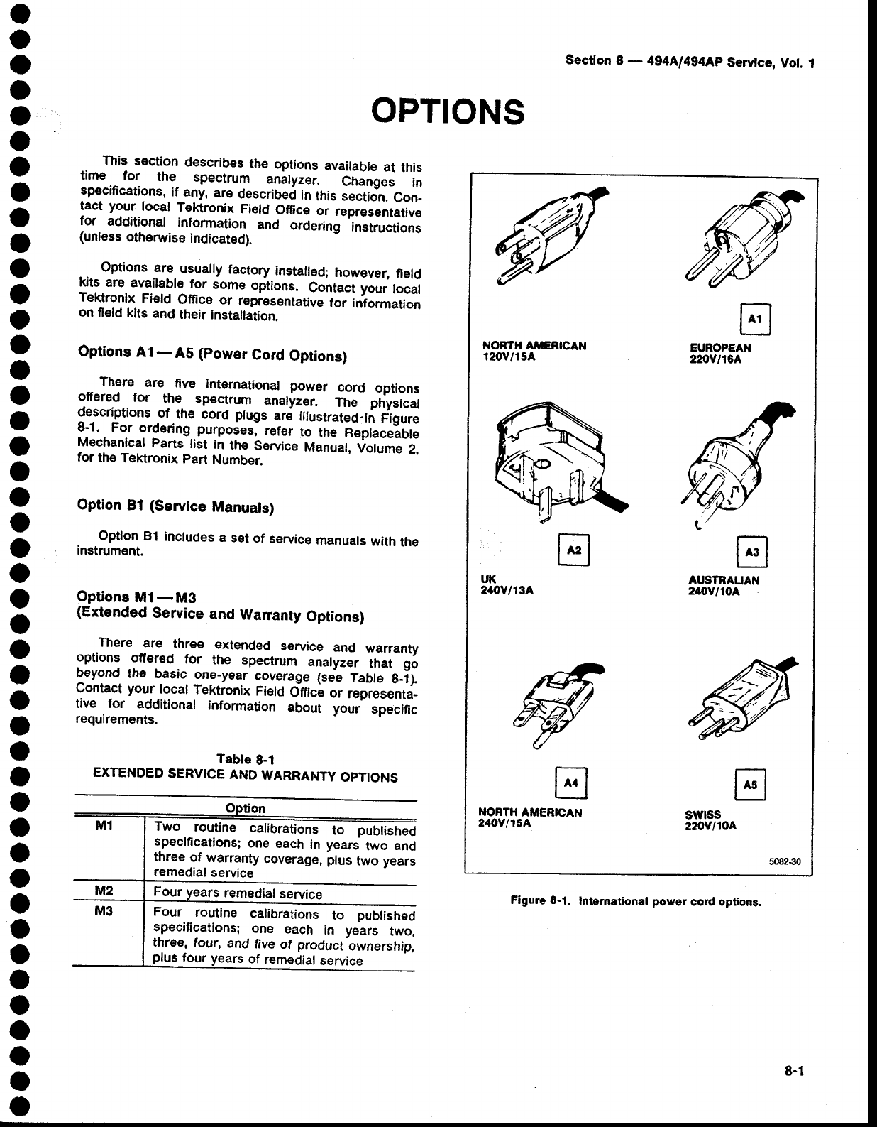
o
o
a
I
o
o
o
a
o
a
o
o
o
I
O
o
o
o
o
o
o
o
o
o
o
o
a
o
o
o
o
o
o
a
o
o
o
a
o
o
o
o
o
o
OPTIONS
This section
describes
the options
available
at this
time
.- for the spectrum analyzer. Ct.ng"" in
specifications,.if
any,
are
described
in
this
section.
Con-
taet your local Tektronix Field Office
or representativ€
for additionat
information
and ordering instructaons
(unless
othenrise
indicated).
Options
are usuaily
factory
installed;
however,
field
kits are available
for some options. Contact your local
Tektronix
Field Office or r€presentative
for information
on
fiEld
kits
and
their installation.
Options A1-AS (power Gord Options)
There are five int€rnataonal
power cord options
offered
.
for the spectrum analyzer, The physical
descriptions
of the cord plugs
ar; iltustrateC-in
Rgure
8-1..
For ordering
purposes,
refer
to the Replaceable
Mechanical
Parts
list in th€ Service
Manual,
Votume
2,
for th€
Tektronix
part Number.
Option Bl (service Manuals)
Option 81 includes
a set
of service
manuats
wath
the
instrument.
Options
Ml-M3
(Extended Service and Warranty Options)
There are three extended service and warranty
options ofiered for the spectrum analyzer
tnat 96
beyond the basic one-year
coverage
{see Table g_i).
Contact
your focal
Tektronix
Field
dtric; or representa-
tive for additional information
about your specific
requlrements.
EXTENDED
sERv'clTlt'D8;ARRANTy
opl oN s
lA1 |
EUROPEAN
220Yl104
|
^'J
AUSTRALIAN
2&Vl10A
swtss
220v1104
}IORTH AMERICAN
120V/154
ut(
2.rcV/134
NORTH
AMERICAN
240V115A
Sectlon
8 - 494[l4g4Ap Servlce,
Vot.
I
Figure 8-1. Intemational power cord options.
Two routine calibrations to publistled
specifications;
one
each
in years
two and
Four routine calibrations to published
specifications;
one each in years two,
three, four, and five
of product
ownership,
plus
four
years
of remedial
service
8-1
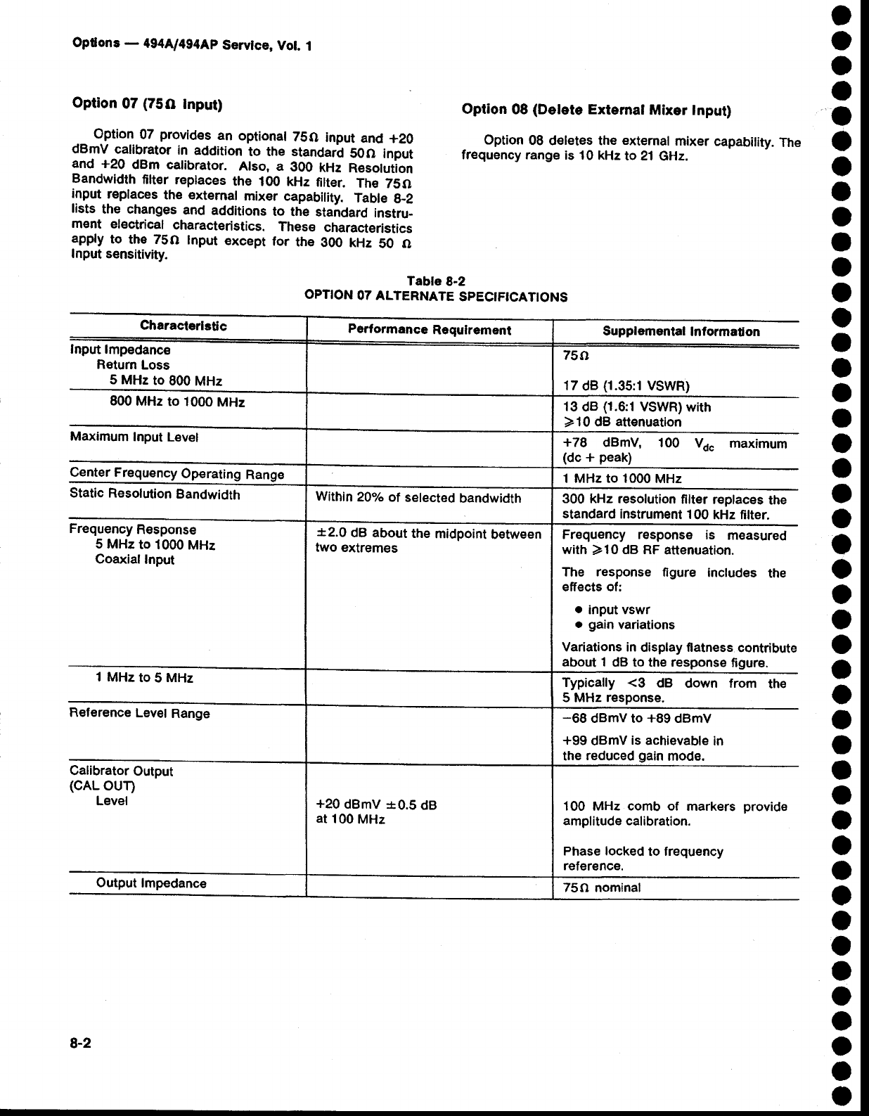
OPTION
07 ALTERNATE SPECIFICATIONS
Within 2ao/o
ol selected
bandwidth
*2.0 dB about
the
midpoint
between
two extremes
+20
dBmV
*0.5 dB
at
100
MHz
Optons - 4944/494Ap
Servlce,
Vol. 1
Option 07 (75O Inpur)
Option 07 provides
an optional 7SO input and *20
dBmV
calibrator
in addition
to the standard
50O input
and +20 dBm calibrator. Also, a 300 kHz Resolution
Bandwidth
filter replaces
the 100 kHz fitter. The 7SO
input replaces
the €xtemal mixer capability. Table g-2
lists the changes
and additions
to the standard
instru-
msnt electrical characteristics. These characteristics
apply to the 75o Input except for the 3@ kHz 50 o
Input
sensitivity.
Option 08 (Delete External Mixer Input)
Option
08 deletes the
ext€mal
mixer
capability.
The
frequency range
is 10
kHz
to 21
GHz.
o
o
O
a
I
o
o
a
o
o
o
o
o
o
a
o
o
o
a
o
o
o
o
o
o
o
o
o
O
a
o
o
o
o
O
o
o
o
o
o
o
o
O
o
8-2
Table
8-2
Characlerlstic
Input lmpedance
R€tum
Loss
5 MHz
to 800
MHz
800
MHz
to 1000
MHz
Maximum
Input
L€vel
Center Frequency
Operating
Rang€
Static Resolution
Bandwidth
Frequency
Response
5 MHz
to 1000
MHz
Coaxial
Input
1 MHz to 5 MHz
Reference
Level Range
Calibrator
Output
(cAL
OUT)
Level
Output lmpedance
Supplemental
Informaton
75(}
17
dB
(1.35:1
VSWR)
13
dB
(1.6:1
VSWR)
with
>10 dB attenuation
+78 dBmV, 100
(dc
f peak) Vo. maximum
1 MHz to 1000
MHz
300 kHz resolution
filter replaces
the
standard
instrument
100
kHz filter.
Frequency response is measured
with )10 dB RF
attenuation.
The response
figure includes the
effects of:
. input
vswr
r gain
variations
Variations in
display flatness
contribute
about 1 dB to the response
figure.
Typically <3 dB down from the
5 MHz r€sponse,
-68 dBmV to +89
dBmV
+99 dBmV
is
achievable
in
the
reduced
gain
mode.
100 MHz comb of markers provide
amplitude calibration.
Phase locked
to frequency
reference.
75o nominal
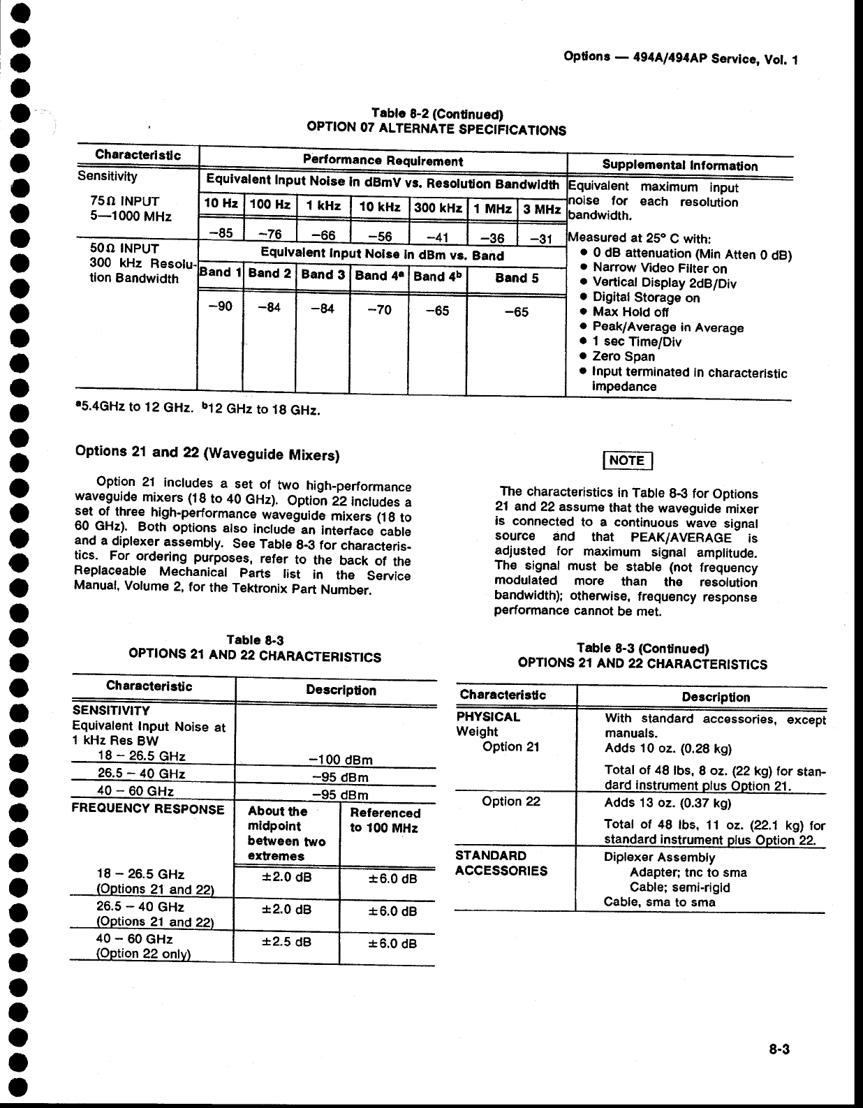
o
o
a
o
o
o
o
o
o
o
O
o
o
I
o
o
O
o
a
o
o
o
o
o
I
o
o
o
I
o
a
o
o
o
O
o
a
o
o
o
o
o
o
I
Optons _ 494Al4g4Ap
Servtce,
Vol. 1
Tabtc
B-2
(Continued)
OPTION
07
ALTERNATE
SPECIFICATIONS
tS.4GHz
to l2 GHz.
bl2 GHz
to 1g
GHz.
Options 21 and 22 (Waveguide Mixers)
Option
21 includes
a set of hrvo
high-performance
waveguide
mixers (18
to 40
GHz).
Optio-n
i2 includes
a
set of-three
high-performance
waveguide
mixers
(1g
to
60 GHz). Both options
also
includJan interface
cable
and
a diplexer
assembly.
SEe
Table
g-O
for characteris-
tics. For ordering purposes, refer to the back of the
Replaceable
Mechanical parts list in the Service
Manual,
Volume
2, for
the
Tektronix
part
Number.
Tabte
&3
OPTIONS
21
AND
22
CHARACTERISTICS
The
characteristics
in
Table
8€ for
Options
21 and
22 assume
that
the waveguide
mixer
is connect€d
to a continuous
wave signal
source and that PEAKIAVERAGE is
adjusted for maximum signal amplitude.
The signal
must be stable
(not frequency
modulated more than the resolution
bandwidth);
otherwise,
frequency
response
performance
cannot
be met.
Table 8-3
(Continued)
OPTIONS
21
AND
22
CHARACTERISTICS
CharacterisUc Descrlpton
PHYSICAL
Weight
Option
21
Option 22
STANDARD
ACCESSORTES
With standard
accessories,
except
manuals.
Adds 10
oz.
(0.28
kg)
Totaf
of 48lbs, I oz.
{22
kg)
for stan-
ion
21.
Adds 13 oz. (0.37
kg)
Total of 48 tbs, 11 oz. (22.1 kg) for
Diplexer
Assembly
Adapter;
tnc
to sma
Cable; semi-rigid
Cable. sma
to sma
8-3
Characterlstc Performanc€
Requlrement Supplemental Information
Sensitivity
75O
INPUT
5-1000 MHz
Eguivatent
tnput
Noi"t ent maximum input
for each resolution
easured
at 25"
C with:
. 0 dB anenuation
(Min
Atten
0 dB)
o Narrow
Mdeo
Filter
on
. V€rtical
Disptay
2dBlDiv
o Digital
Storage
on
o Max
Hold
off
o Peak/Average
in Average
. 1 sec
Time/Div
o Zero Span
. Input
terminated
in
characteristic
impedance
10
Hz 100
Hz 1
kHz 10
kHz 300
kHz I MHz 3 MHz
-85 -76 -66 -s6 -41 -36 I -31
5OO
INPUT
300 kHz Resc
tion
Bandwidth
Equlvalent
Input
Nolso
In
dBm
vs. Band
land 1Band 2Band
3Band 4a Band 4b Band
5
-90 -84 -u -70 -65 -65
SENSITIVITY
Equivalent
Input
Noise
at
1
kHz
Res
BW
Optione
- 494A/494Ap
Service,
Vot.
1
Option 39 (Sitver Battery)
. Option 39 provides a silver battery for the
instru_m€nt's
battery-powered
memory. The battery
life
at +55"C is 1-2 years
and 2-5 years
at +2SoC.
W€
recommend
removing
the silver batteries
during
long-
term storage.
Option 41 (Digitat Radio)
Option
41 inctudes
the
following
teatures
to provide
extra measurem€nt
capabilities
for Digital
Microwave
Radio. Table 8-4 tists the changes
troh tne standard
instrument.
o A wider
bandwidth
presel€ctor
provides
better
sig-
nal symmetry
in
the
digital
radio
bands.
o A narrow
video
fitter
(approximately
1/3000th
of the
resolution
bandwidth)
improves
amplitude
variation
analysis
at specific
frequency
spans
that are
unique
to the digital
radio
measurements.
o llprovcd frequency span/div accuracy at s
MHz/div
span provides
accurate
signal
bindwidth
measurements.
O
o
o
o
a
o
o
a
o
o
o
o
o
o
o
a
o
o
o
o
o
o
o
o
a
o
a
o
I
t
a
o
o
o
o
o
o
o
o
o
o
o
o
o
8-4
Option 42 (110
MHz lF Outpur)
Option 42 provides
tor a rear-panel
110
MHz
tF
sig-
nal
with a bandwidth
greEter
than
5 MHz,
which
makes
the spectrum analyzer suitable for broadband swept-
rEceiver
applications. Table 8-5 lists the electrical
characteristics
of the
110
MHz output.
Oplion 45 (MATECO)
This option
provides
the
spectrum
analyzer
with
the
software/firmware nec€ssary to meet Modular
Automated Test Equipment Compatibitity Options
(MATECO). A MATECO Programmers Manual is
included
as
an accessory
with
this
option.
Option 52 (North American 220V,
Option 52 provides a North American 22O V
configuration
with the standard
pow€r cord. The fuses
are
replaced
with 2A
slow
blow.
Table 8-4
OPTION
41 ALTERNATE
SPECIFICATIONS
Gharacteristic
FREOUENCY
Frequency
Span/Div
Accuracy
Video Filter
Narrow
Preselector
Filter
Bandwidth
1.7
GHz
to 5 GHz
5 GHz
to 16
GHz
Hz
to 2'l
Supplemental Inlormation
At center frequency of 6 GHz and 11
GHz
Measured over
th€
center
6 divisions
of
3O
Hz (1i3000th)
with 100
kHz reso-
3O MHz minimum
35
MHz
minimum
5 MHz/div,
within
*1%
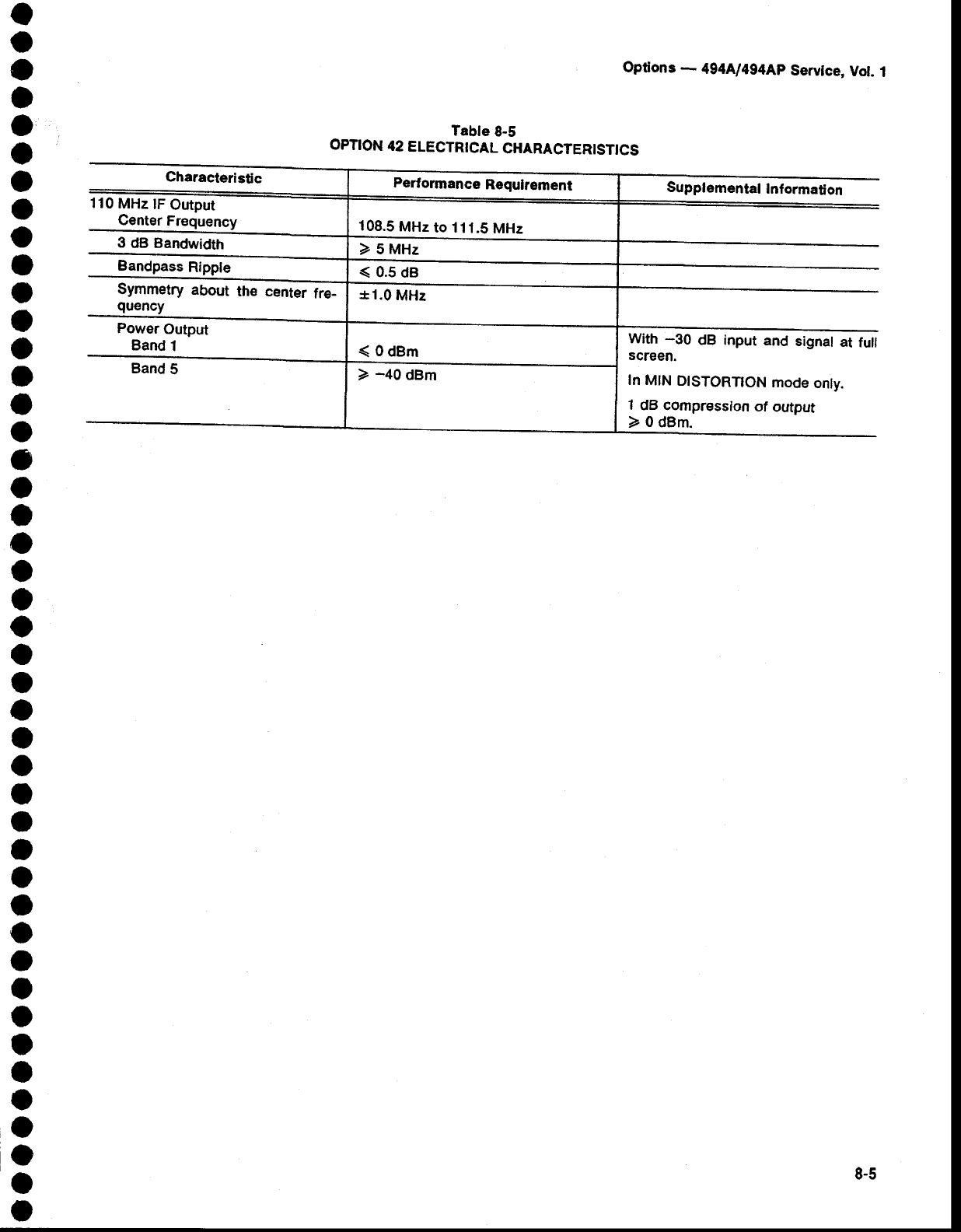
o
a
a
a
o
o
o
o
o
I
o
o
o
I
o
o
o
o
o
o
a
o
o
o
I
o
a
o
o
O
a
o
a
o
I
I
a
o
a
a
O
o
o
a
Opdons
_ 494A/4g4Ap
Servlce,
Vol.
1
Tabte
8-5
OPTION
42
ELECTRICAL
CHARACTERISTICS
Characteristic Performance
Reguirement Supptemental
Information
tu Mnz
tF
gutput
Center
Frequency
goesanoffi
B"ndp""" C[ptJ--
symmetry
"ooultn"Gffi
quency
Power
Output
Band
1
108.5
MHz
to 111.5
MHz
)5MHz
< 0.5 dB
t1.0
MHz
(0dBm With -30 dB input
and signat
at futl
screen.
In
MIN
DISTORTION
mode
onty.
1 dB compression
of output
) 0
dBm.
Band
5) -40 dBm

o
o
o
a
I
o
o
I
O
I
I
I
o
o
o
I
I
o
o
o
o
o
o
o
o
o
a
o
I
a
o
o
a
o
o
a
o
o
t
o
o
o
o
a
o
o
a
a
O
o
a
I
o
t
o
O
o
o
I
o
a
t
o
o
a
o
o
o
o
a
a
o
o
o
a
o
o
o
o
O
o
t
I
o
o
o
o
I
GLOSSARY
.._-Il"^^1"_l':,*ing
gtossary
is presented
as an aid to
understand
the
terms
as they
aie used
in
thi" do"urn"nt
and
with
reference
to spectrum
anatyzers.
GENERAL
TERMS
Center
Frequency.
That frequency
which
corresponds
to the center
of a frequency
span,
expresseO
in hertz.
Baseline
cftpper (rntensrfier).
A means
of increasing
the
brightness
of the
signat
retativ"
i;l;; basetine
por_
tion
of the
display.
dBc.
Decibels
referenced
to carrier
level.
1_8i.. .A
unit_
to express
power
level
in decibels
refer-
enced
to 1 milliwatt.
dBmV. A unit to express voltage
levels
in decibels
referenced
to 1 millivolt
dBpV. A unit to express voltage levels in decibets
referenced
to 1 microvolt.
Efrectlve.
Frequency_.T:1g.".
That range of frequency
over which the instrument
performanie
is specified.
The
lower
and
upper
limits
are
"if.""r"t:in n".tr.
Envelope
Display.
The
display
produced
on a spectrum
anatyzer
when
the resotutibn
bino*iOt ii greater
tnan
the
spacing
of the
individual
trequenci
"o,ipon"nt".
Freguency
Band. A part of effectjve
frequency
range
over
which
the
freouency
can
be
adlusted,
Lxpressed
in
hertz.
Full
.Span
(Maximum
Span). A rnode
of operation
in
which
the spectrum
anatyzer
"""n, "n "ntir" tr"qu"n"y
band.
lnterm-odulation
Spurious
Response
(lntermodulation
Distortion
- tMD). An..unwanre;
;d;i;* anatyzer
response
resulting
from
the mixing
of the
nth
order
fre_
quencies,
due
to non-linear
elemints
ot in" spectrum
analyzer, the resultant unwanted ,".fonr" being
displayed.
Llne Display. The display produced
on a spectrum
anatyzer
when
the
resolution'bandwidih
i" t"." than
the
spacing
of the signar
ampritudes
of the
individuar
fre-
qu€ncy
components.
Llne
SpectruT.
A spectrum
composed
of signal
ampli-
tudes
of
the
discrete
frequency
components.
Markers.
The
instrument
uses
three
typ€s
of markers:
Waveform
Markers. _ When
the Marker
function
is enabled, it provides a movable cursor with
readout
of frequency
and amplitude
at the marker
position.
When
the
delta
marker
mode
is enabled,
a
second marker allows operations and readout
between the two_
marker positions. (Also see
Waveform
Marker
Terms.)
Update
Marker. - Marks
the
current
sweep
posi_
tion in a digitat
storage
disptay
as the disptiy is
being
updated.
Video
Mark
9{"_rryl VTDEOIMARKER
inpul from a Tektronix
1405 Television
Sideband
Analyzer. The Video
Markers
mark frequencies
of interest
on the
televi-
sion
signal.
Maximum
Safe
Input
power
WITHOUT
DAMAGE...The
maximum
power
apptied
at
the input
which
will
not cause
degiadation
oi the
instrument
characteristics.
WITH
DAMAGE.
The
minimum
power
applied
at the
input
which
will
damage
the
instrument.
'
Pulse
Sfetcher. A pulse
shaper
that produces
an out_
put pulse,
whose duration
is greater
than that of the
input pulse,
and
whose
amplitude
is proportional
to that
of
the
peak
amplitude
of
the
input
pui"e.'
Scanning
Velocity.
Frequency
span
divided
by sweep
time and
expressed
in
hertz
pir second.
Signal
ldentitier.
A means
to identify
the spectrurn
o,
the
input
signal
when
spurious
,esponses
are
possible.
Video.
The
term
is used
here generally
to mean
a sig_
nal
after
the
detector
stage.
lt can
also
be used
more
specifically
to mean
a baseband
(zero
carrier
frequency)
television
signal.
Video
Filter.
A post
detection
low_pass
filter.
Zero
Span.
A mode
of operation
in
which
the frequency
span
is
reduced
to
zero.
Appendix A - 4g4Al494Ap
Service,
Vol. 1
A-1
FREQUENCY
TERMS
Display
Frequency.
The
input
frequency
as indicated
by
the spectrum
analyzer
and
expressed
i; hertz.
Frequency
Span (Dispersion).
The magnitude
of the
frequency
band
displayed,
expressed
in-hertz
or hertz
per
division.
Frequency
Llnearity
Error.
The
error
of the relationship
between
the frequency
of the input
signal
and the fre-
quency
displayed (expressed
as
a ratio).
Freguency
Drlft Gradual
shift or change
in displayed
frequency over the specified time Oue to internal
changes
in the spectrum
analyzer,
and expressed
in
hertz per second,
where
other
conditions
remain
con-
stant.
lmpulse
Bandwldth.
The displayed
spectral
level
of an
applied
pulse divided
by its spectral
voltage
density
level
assumed
to be flat
within
the
pass_band.
Residual
FM
(lncidental
FM).
Short
term displayed
fre-
quency
instability
or jitter due
to instability
in th-e spec_
trum analyzer
local
oscillators,
given
in terms
of pLak-
to-peak
frequency
deviation
and expressed
in hertz
or
percent
of the
displayed
frequency.
Shape Factor (Skirt Selectivlty).
The ratio of the fre_
quency
separation
of the
two (60
dBi6 dB)
down
points
on the response curve to the static resolution
bandwidth.
Static
(Amplifier)
Resolutlon
Bandwldth.
ThE
specified
bandwidth
of the spectrum
analyzer's
response
to a cw
signal,
if sweep
time is kept substantiaily
long. This
bandwidth
is the frequency
separation
of two points
on
the response
curyer
usually
6 dB down,
if it is measured
either
by manual
scan (true
static
method)
or by
using
a
very
low
speed
sweep
(quasi-static
method).
Zeto Pip (Response).
An output indication which
corresponds
to zero
input
frequency.
AMPLITUDE
TERMS
Detlectlon Coeflicient. The ratio of the input signal
rnagnitude
to the resultant output indication. Tne ratio
may be expressed in terms of volts (rms) per division,
decibels per division, watts per division, or any other
specified
factor.
Dlsplay Reference Level A designated
vertical position
representing a specified input level. The level may be
expressed
in dBm, volts,
or any
other
units.
Gfoesary
- 494[l4g4Ap
Service,
Vol.
1
Display Flatness. The unwanted variation of the
displayed
amplitude
over a specified
frequency
span,
expressed
in
decibels.
Relative Display Flatness. The display ftatness
measured
relative
to the
display amplitude
at a
fixed
frequency
within
the frequency span,
expressed
in
decibels.
Display flatness is closely related to fre-
quency response. The main difference
is
that
the spectrum
display
is not recentered.
Display Law. The mathematical law that d€fines the
input-output
function of the instrument.
The following cases apply:
Llnear - A display in which the scale
divi-
sions are a linear
function
of the input sig-
nalvoltage.
Square law {power} - A display in which
the scale divisions
are a linear
function
of
the input
signal
power.
Logarithmic
- A display in which
the scale
divisions are a logarithmic
function of the
input
signal
voltage.
Dynamic Range. The maximum ratio of the levels of
two signals simultaneously present at the input which
can be measured to a specified accuracy.
Display Dynamic
Range. The maximum
ratio
of the
levels of two non-harmonically
related sinusoidal
signals
each of which can be simultaneously
meas-
ured on the screen
to a specified accuracy.
Frequency Response. The unwanted variation of the
displayed
amplitude over a specified
center frequency
range,
measured at the center frequency,
expressed
in
decibels.
Gain Compresslon. Effect seen at an input
level
where
the analyzer
circuits
have less gain
than
their small sig-
nal values. This is usually specified at the 1 dB
compression
point
in
terms of the input
level required
to
reduce
the gain
by 1 dB.
Input lmpedance. The impedance
at the desired input
terminal. Usually expressed in terms of vswr, return
loss, or other related
terms for low impedance
devices
and resistance-capacitance parameters for high
impedance
devices.
I
o
o
O
a
o
O
o
o
o
o
I
o
o
t
o
I
a
o
o
o
o
o
o
o
o
t
O
t
o
o
o
o
o
o
O
o
I
a
o
o
o
I
o
A-2
o
o
o
O
o
o
t
o
o
t
o
I
o
O
o
o
o
I
o
o
O
o
o
a
o
a
o
o
I
O
I
o
I
o
o
I
I
o
o
O
o
o
o
I
Sensitvity.
Measure
oJ
a.
spectrurn
analyzef
s ability
to
display
minimum
rever
signars,
"*pi".J"o in vorts
or
decibets. Intermediate.
tr"qu"n"V
-ifei bandwidth,
display
mode,
and
any
other
innueniinji"'.to* must
be
given.
Spu.rious Response.
_.
A respons€ of a spectrum
analyzer
whErein
the
displayed'frequency
is not
related
to the
input
frequency.
Hum Sidebands. Undesired responses cr€ated
within the spectrum
analyzer,
"pp"urlng on the
display, that are separated trom the desired
response
by the fundamental
or harmonic
of the
power
line
frequency.
Noise Sldebands.
Undesired
response
caused
by
noise
internal
to the
spectrurn
analyzer
appearing
on
the
display
around
a desired
,".ponr".
Resldual Response.
A spurious
response
in the
absence.of
an
input
signal.
(Noise
und:
r.ro pip
are
excluded.)
DIGITAL
STORAGE
TERMS
Digitatfy
Stored
Disptay-
A.disptay
method
whereby
the
displayed
function
is held_.in'a'digital
memory.
tne
display
is generated
by reading
the
dita ouf
ot mernory.
Digltally-
Averaged
Display.
A disptay
of the average
value of digitized
data computed
by combining
serial
samples.
Multiple
Disptay
Memory.
A digitaily
stored
disptay
hav,
in_g_
multiple
memory
sections
wtrictr
""n b" displayed
separately
or simultaneously.
Clear (Erase).
presets
memory
to a prescribed
state,
usually
that
denoting
zero.
Save.
A function
which.
inhibits
storage
update,
saving
existing
data
in a section
of a multif,le
,i"rory 1".g,,
Save A).
Glossary
_ 4g4Al4g4Ap
Service,
Vol.
1
View (Display).
Enables
viewing of contents of the
chosenmemory
section
(e.g.,
'.Vidw
A, displays
the con-
tents
of memory
A; ',View
B" displays
the contents
of
memory
B).
Max Hold (peak Mode),
Digitally
stored
display
mode
which,
at each
frequency
addresi,
compares
thsincom-
ing signal level to the stored level and retains
the
greater.
ln this mode,
the display
indicates
the peak
lev€l at each frequency after
-
several successive
sweeps.
Scan
Address.
A number
representing
each
horizontal
data position increment on a direited Ueam type
display.
An address
in a memory
is associated
with
each
scan
address.
Volatile/Non-volatile
Storage.
A volatile
storage
system
is one
where
any
total loss
of power
to the
system
will
result in a loss of stored information. Non-volatite
I"Tory is not subject
to the instrument
power
supply
for its
storage.
WAVEFORM
MARKER
TERMS
Live Trace. Any combination of the A trace and/or the
B trace when SAVE
A is off.
Active Trace. Live Trace or the B-SAVE A trace (a
trace recalled
into B is not an active
trace).
Inactive Trace. SAVE A trace or a trace recalled into
the B display
before the sweep is started.
Primary Marker. The marker displayed in the Single
Marker mode whose frequency and/or position is
gllseo when tuning with the CENTER/MARKER
FRE_
QUENCY
control. When two markers are displayed,
the
brightest
marker is the primary marker.
Secondary Marker. The "second,, marker; displayed
only
in
the Delta
Marker
mode.
A-3

o
o
o
o
a
o
o
o
O
o
o
o
o
o
t
o
o
a
o
a
a
o
o
a
O
o
t
o
I
o
C
o
I
o
t
o
o
o
o
o
o
o
o
o
o
o
a
o
o
o
o
I
I
o
O
I
o
o
I
o
o
I
o
o
O
o
o
O
a
a
t
o
t
a
I
o
o
O
a
I
I
o
I
o
o
O
o
I
REVISION
INFORMATION
Manual
Part
No. 07G556O-00 Flrst
prtnilng JAN
1987
hduct Revleed
Manual
Insert
Status
CHANGE
REFERENCE
SEP
1987
FEB
1988
MAY
1988
JUN
1988
MAY
1990
JUN
1990
SEP
1991
c11887
M63911
c2lsge
M66071
c21590
C2l590
REVISED
c1-991
Effective
Effective
Effective
Efiective
Effective
Effective
Effective
Page 1 of 1

o
o
o
o
a
a
o
a
o
o
o
o
o
o
a
o
o
I
o
a
o
o
o
a
O
a
t
o
I
o
t
o
o
o
I
I
o
o
I
o
o
o
o
t
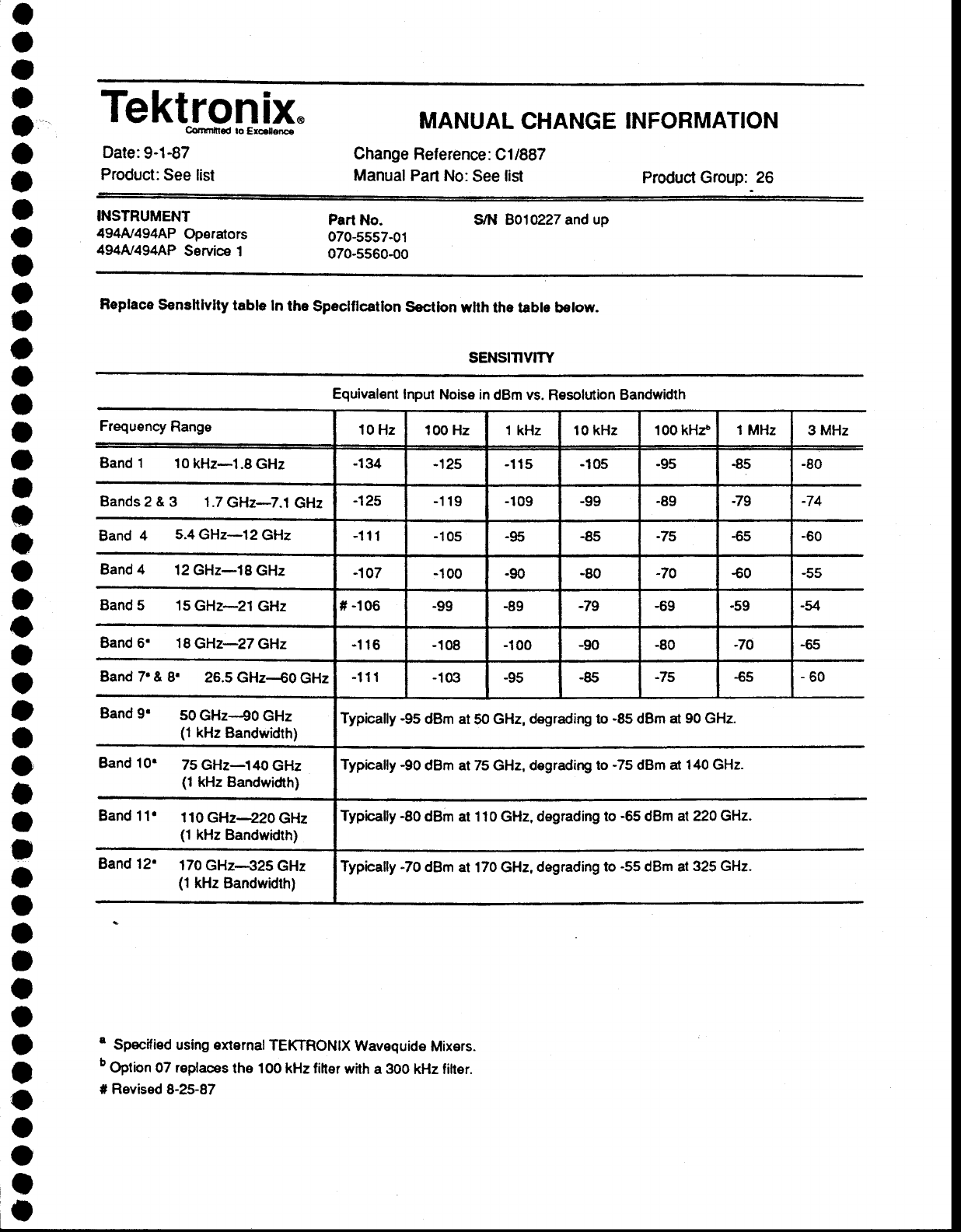
Tektronix.
Cornnt|ncd to Ercdl€E
Date:9-1-87
Product:
See
list
MANUAL
CHANGE
INFORMATION
Change
Reference:
C1
1887
Manual Part
No:
See
list product
Group:
26
INSTRUMENT
494N494AP
Op€rators
494N4944P
Service 1
Part No.
070-s557-01
070-5560-00
gN 8010227and
up
Feplaca
sanshlvlty
table In the speclflcailon secilon wlth the tabte betow.
SENSmV|TY
o
o
o
I
)
o
t
o
o
I
t
I
o
o
I
o
o
I
o
I
a
a
o
o
o
o
a
o
a
o
I
I
o
I
t
I
o
o
t
o
o
o
I
I
' Specified
using externalTEliTRONlX
Wavequide
Mixers.
b
Option
07
replaces
the 100 kHz filter
with
a 300
kHz fitter.
# Revised
8-25-87
Equivalent
Input Noise in dBm vs. Resohrtion
Bandwidth
Frequency
Range 10 Hz 1O0 Hz 1 kHz 10 kHz 10O kH2f 1 MHz 3 MHz
Band 1 10
kHz-1.8
GHz -134 -12s 115 -105 -95 €5 -80
Bands2
&
3 1.7
GHz-7.1
GHz -12s -1
19 -109 -99 -89 :19 -74
Band 4 5.4 GHz-12 GHz -11
I-1
05 -95 -85 -75 €5 -60
Band
4 12 GHz-18
GHz -107 -100 -90 -80 -70 €0 -55
Band
5 15
GHz-21 GHz #
-106 -99 -89 -79 -69 .59 -54
Band
5' 18
GHz-27 GHz -1
16 -108 -100 -90 -80 -70 -65
Band 7'& 8. 25.5 GHz-€0 GHz -11
1-103 -95 -85 -7s €5 -60
Band
9. 50
GHz-€0 GHz
(1
kHz
Bandwidlh)
Band 10' 75 GHz-140 GHz
(1
kHz Bandwidth)
Band 11' 11OGHz-ZZ0GHz
, (1
kHz Bandwldth)
Band 12' 170
GHz-825 GHz
(1
kHz
Bandwidth)
Typically
-95
dBm at
50
GHz,
degrading to -85
dBm at
90 GHz.
Typically
-90
dBm at 75 GHz, degrading
to -75
dBm at 140 GHz.
Typkafly
-80
dBm
at 1
'l
0
GHz,
degrading
to -65
dBm al220 GHz.
Typlcally
-70
dBm
at 170 GHz,
degrading
to
-55
dBm at
325 GHz.

o
o
o
o
t
o
I
a
O
o
o
I
o
o
a
I
o
a
o
o
O
a
o
o
o
o
o
o
I
o
t
o
t
a
t
o
o
o
o
o
o
o
o
I
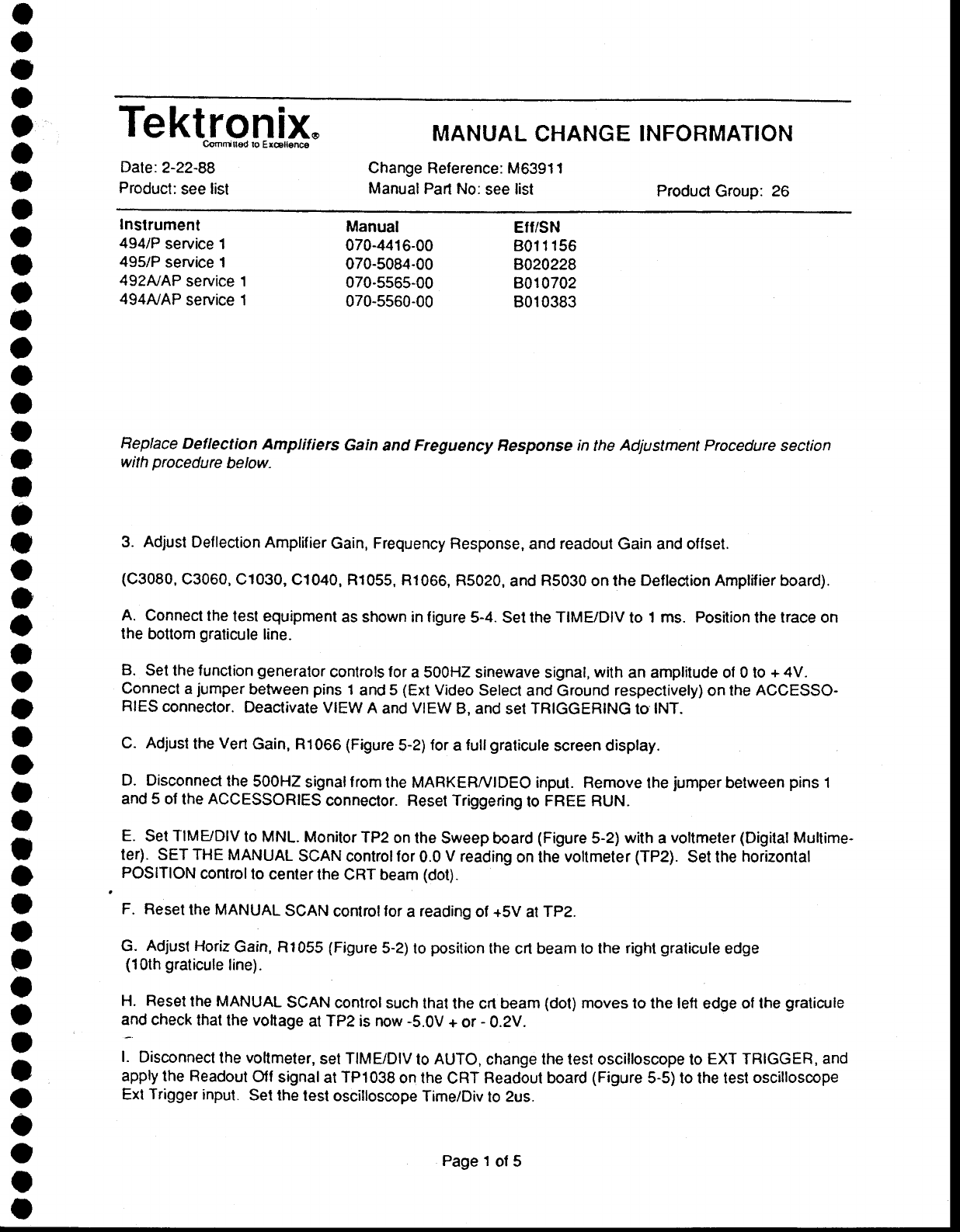
Tektronix"
Cdmfrittsd to Erca{ence
Date:2-22-88
Producl:
see
list
MANUAL
CHANGE
INFORMATION
Change Reference: M6391 1
Manual
Part
No:
see
list product
Group:
26
I
a
I
o
o
a
o
a
o
I
o
o
o
o
a
o
o
I
)
o
o
t
a
O
o
o
a
o
a
o
I
o
o
o
o
o
a
O
o
o
o
o
t
t
Inslrument
4941P
service 1
495/P
service 1
49?NAP
service
494AIAP
service
Manual
070-4416-00
070-5084-00
070.5565-00
070-5560-00
Efr/sN
801 1 156
8,020228
8010702
8010383
1
't
Replace
Deflection
Amplifiers Gain
and
Freguency
Besponse
in
the
Adjustment
Procedure section
with
procedure
below.
3. Adjusl
Deflection Ampli{ier
Gain,
Frequency
Response,
and
readout
Gain and offset.
(C3080,
C3060,
C1030, C1040,
R1055, R1066,
R5020,
and
R5030
on the
Deflection
Amplifier board).
A. Connect
the
test equipment
as shown in figure
5-4.
Set
the TIME/DIV
to 1 ms. Position
the
trace
on
the
bottom
gratiarle
line.
B. Set the funclion
generator
controls
for
a 500H2 sinewave
signal,
with
an amplitude of 0 to
+ 4V.
Connect
a
jumper
between
pins
1
and
5
(Ext
Video
Select
and Ground
respectively)
on the
ACCESSO-
FIIES
connector.
Deactivate
VIEW
A
and
V|EW
B,
and sel
TRIGGERING
to
tNT.
C. Adjusl
the
Vert
Gain, R1066 (Figure
5-2)
for
a
fuil
graticute
screen disptay.
D. Disconnect
the
500H2
signallrom
the MARKERA/IDEO input. Remove
the
jumper
between
pins
1
and 5 of
the
ACCESSORTES
connector.
Reset Triggering
lo
FREE RUN.
E. Set
TIME/DIV
to MNL.
Monitor
TP2
on
the Sweep
board
(Figure
5-2)
with
a
vollmeter
(Digital
Multime-
te4. SET
THE
MANUAL
SCAN
controlfor
0.0
V reading
on the
voltmeler
(TP2),
Sel lhe
horizontal
POSITION
control
lo
center
the CRT beam
(dot).
F. Reset
the MANUAL
SCAN
controtfor
a
reading
of +5V
alTpz.
G. Adjust
Horiz
Gain,
R1055
(Figure
5-2)
to
position
the
crt beam
to the
right
gralicule
edge
(1Oth graticule
line).
H. Reset
the MANUAL
SCAN
control
such that
the crt beam
(dot)
moves lo the left
edge
ot the
graticule
and check
thal
the
voltage
at TP2 is now
-5.0V
+ or
- 0.2V.
l. Disconnect
the vollmeter,
set
TlMgDlV
to
AUTO,
change the tesl oscilloscope
to
EXT
TBIGGER,
and
apply lhe Readout
CIf
signalat TP1038
on the
CRT
Fleadoul board
(Figure
5-5) to
the
lest
oscillosmpe
Ext
Trigger
input.
Set the
test oscilloscope
Time/Div
to 2us.
Page 1
ol 5
Product:
see
list Date:2.22-88 Chg.
Ref. M63911
J. Set the Spectrum
Analyzer
controls
for
a lriggered
sweep,
then
switch
the sweep
oft by
activating
SINGLE SWEEP,
and
ensure
READOUT
is
on.
K. Monitor
lhe drains
(metal
tabs)
of
04040 or
Q4030,
on lhe dellection
Amplifier board,
with
test oscillo-
scope. See Figure
5-6
L. Adjust
C1040 for
best
frequency
response (no
overshoot
or
roll
off)
as
viewed on the test
oscilloscope.
M. Monitor
the Drains
(metal
tabs)
of Q4020
or Q4010,
on the
Amplifier
board,
with
the tesl oscilloscope.
N. Adjust
C1030
(Figure
5-6
tor
the
best response).
O. Monitor
the Drains
(metal
tabs) of
02090
or
Q1090, on the
Deflection
amplifier
board,
with
the lest
oscilloscope.
P. Adjust
C3080
for
best response.
Q. Monitor
the drains
(metal
tabs)of Q1070
or
Q2070, on the
Deflection/amplifier
board,
with
the test
oscilloscope.
R. Adjust
C3060
lor
best response.
S. Disconnect
the test
oscilloscope.
Check
lhe appearance
of
the letter
"2"
in GHZ of the
frequency
readout,
and if
necessary,
readjust
C3060
and
C3080
(vertical
output)
for
the
straightest
top on the
letter
"2". Note:
The
oscilloscope
probe
may
alter
the
response
and
alter
removing
the
oscilloscope
probe,
adjustment will
be
necessary.
T. Set the VERTICAL
DTSPLAY
to
LlN, TIME/DIV
to
MNL,
the
REF LEVEL
for
100uv, with
the
MANUAL
SCAN
conlrol set fully
clockwise.
U. Adjust
C1030
and
C1040
for the best REF
LEVEL readout
(straightest
letters
and
numerals). Posilion
the
MANUAL
SCAN
back
and
forth
between
lhe
clockwise
and counter
closkwise
position
and continue
to
adjust
C1030
and
C1040 for
best
response.
V. Adjust
R5020,
R/O
GAIN
and
R5030,
R/O
OFFSET
for
best
placement
of the
readout
characters
(top
and bottom)
depending
on
whether
or not
the
crt
has
a lull
graticule
or a
reduced
graticule.
Note:
Set
the firsl
two row
of readout
characters
iust
above the top
graticule
line and
set the
last row
of
readout
characters
iust
below
the bottom
graticule
line
on
Reduced
graticule
inslruments.
o
o
o
o
a
o
o
o
o
t
o
o
o
o
o
o
I
a
a
o
o
a
o
a
o
o
O
o
O
a
o
o
t
a
o
o
o
o
o
o
o
o
I
o
Page
2
of 5

o
o
I
o
o
o
o
o
o
o
o
I
o
o
I
o
o
I
o
a
o
o
o
o
o
t
o
o
I
o
I
O
o
o
t
o
o
o
I
o
o
o
o
I
Product:
see llst date:2-22-88 Chg. Ref:
M6391r
Replace
the
description
for
the Deftection
Amptifiers
(Diagram
27) with
the
tottowing.
DEFLECTION
AMPLIF|ER
(Diagram
278)
Refer
lo ihe
block
diagram
adjacenl
to Diagram
27
as
well
as the schematic diagram. The
Deflection
Amplif
ier
receives
verlical
signal inlormation
trom
the vertical
section of lhe Digital
Storage of the
Video
Processoi,
and
horizonlalorsweep
board.
The
Readoul
data forthe
display comes
tromthe
CR1 Readout
circuits. The
output
of the Deflection
Amplifier
drives
the
crt
dellection
plates.
The amplitiers contain
lhe switching
circuits
necessary
lo
perform
the selection
functions
and
they
also contain the amplifier
stages
needed
to
product
the
defleclion
plate
drive
signals.
Horizontal
Section
Signal
lines
HORIZONTAL
SIGNAL (from
lhe digitatstorage
circuits through
edge connector
pin
49)
and
Sweep
(from
the
Sweep
circuit
through
edge
connector
pin
51)
are
apptied
to switCh
U7O55A. U705s,
under
conlrolof
the
STORAGE
OFF
signal
(from
the
digitalstorage
circuits
through edge connectorpin 7),
setects
eitherthe
HORIZONTAL
S|GNALorSWEEPinput.
The
SWEEP signatis setectedwhenthe
STORAGE
OFF
line is
pulled
low.
Resistive
divider
R7065
and R7070 reduce
the selected signal
trom
1V/div
to o.Sv/div.
U7073
buff
ers the
selected
signal.
The
sefected
signal
goes
out to
the
HORTZ
OuT
rear-panet
conneclor
via
pin
1
and 2
on
P6100,
P6090
and
pin
48
of
the edge connector.
U7073 appties
the signat
to switch
U70558.
The
HORIZ
R/O
OFF
signal, trom
the
Crt
Readoul
selects between
these two
signati.
When
R/O is floating
or
pulled
high,
the
switch
transmils
the signal lrom
buffer
U7073 to
lhe shaper.
When
the
tine
is
puled
tow,
it
selects
the
HORIZONTAL
R/O
signat.
U7055
applies
the signal
to a shaper
network
lo compensate lor non-linearity
in the crt deflection
characteristics.
This
network
consisls
of
resistors
R5059,
R5058, R50S7,
R4061, iaosg, and
R5062,
plus
diodes
CR4052,
CR4051
,
CR4958,
and
CR4056. The
HORIZONTAL POStTtON
vottage,
from
the
f ront
panel
via
edge
conneclor
pin
47,
through
resistor
R5056,
is
applied to the shaper circuit
so tne
shape conection
lactor
relates
lo
the
crt deflection.
The
shaped
signal
is
then
applied
lhrough
preamplifier
U2055 to
the def
tection
amplitier circuits. HORTZ
gain
adjuslment
R1055,
calibrates
lhe
amount
of
gain
compensation required for
proper
deflection
sensitiviiy.
The
horizontal
detlection
amplilier
consists
of two circuits
similar to each other, one
for
each
horizontal
deflection
plate.
One
circuit
is an
inverting
amplitier,
the
other
operates
in-phase.
Inputs
to U2030
of the
inverting
side
are
through
the
paraltel
combination
ol resistors
R1
039 and R1038
and capacitor C1040. The
series
conneclion
of resistor
R1038
and
variable
capacitor
Cl040 provides
high-frequency response
compensatio
n -
capacit
or c2047
controts
high{requency
f
eedback.
fnpul
lo
lhe
non-inverting
side
of the
amplifier is
through resistor
R1025 to
u2030.
R1o?'zand
R2020
set
the
dc level
for
the feed-back
loop
to
the
plus
input
side of the
amplifier.
Variable
capacitor
C1030
provides
adjustment
to sel
lransient
gain.
High
frequency
feedback
is
controlled
by capaciior C20tO.Gain
ol each
amplifier
section is
approximately
20.
(Horizontaldellection
sensilivityof
lhe crt
is
approximately
21.3v/div
per
side.)
Signalswith
a
low
rate
of
change
drivethe
oulput FETtransistorsthrough
R3038,
asthe
rate
ol
rise
increases,
the
drop
across
R3040
increases
and when
it reaches
0.6V,
either 03047
or e3046 biased
on.
These
transislors
provide
high
current
drive for
the
output
lransislors. When
the signal
rate
ol change is low, 04030
drives
the
crt defleclion
plates
and
Q4040
provides
bias currenl
for
the amplitier,
As
the
rate
or
rise
increases,
949?1
couples
the
signalto
the
gate
of 04040.
04040
provides
the
posilive
drive to the
deflection
ptate,
and
04030
provides
the negative
drive. Each
output
transislor
can
provide
a 200V
excursion
in
approximately
1
ps.
Page
3
of 5
Product:
see
llst Dale:2-22-88 Chg.
Ref: M63911
The
standing
cunent
on the horizontal
amplifier Moslets
is
established
by a resistive
divider
R4046,
R3045,
and
R5038
as
lollows. The
base
of
Q5040
is
set 3.5
volts negative
wilh respect
to the
+300
volt
supply.
The
voltage
drop across
85045
is
then 3
volts
and the
resulting
emitter
currenl
is 2.0ma.
Current
from
the
-15V
source through
resistor R2041
sets the
output
level. Feedback
resistor
R2049
sets
this
outpul
level
at
approximalely
142 volts. Diodes
CR2040,
CR3040,
and
VR4030
provide
transient
voltage
protection
during
turn
on and
under
fault condition.
Capacitor C2031 with
resistor R2035 shape
the
phase
response
of U2030.
Operation
ot the
left
drive
(non-inverting)
section
is
basically
the same
as the
right
drive
(inverting)
section.
Vertical
Section
VIDEO FILTER
OUTfromtheVideo
Processor,
andVERT|CALS|GNALfromlhe
DigilalStorage
are
rouled
through
switch
U60554, under
control of the
STORAGE OFF signal
from lhe
Digital
Storage
board.
Note that
the
video filter
out
signal
is
butfered by U7065 to
prevent
a
change
in
load transients
f
rom aftecting
the signal
level.
A
high
on the STORAGE OFF
line
selects the buffered
VIDEO
FILTER OUT
SIGNAL,
and a
low selects
the
VERTICAL
SIGNAL.
U6065
inverts
the selected
signal
and clamps
it to
ground.
Both
the
VIDEO FILTER
OUTandtheVERTlCAL SlGNALarespecilied
at0.SVtdivwith 0Vforthe
baseline
andpositivevohagesabove
the
baseline.
The
signal
is
re-inverted and olfsel
by bufler U6073 so
cenler
screen
represents
0V.
Buffer U6073
supplies
a
sample
of
this
centered
signallo the
rear-panel
VERT
OUT
connector
via
pins
1 and
2 ol
P7075 and edge
connector
pin
46.
The
output
of u6073 is
also applied through
switch u60558,
when the
R/O
OFF
line
is high,
to
the
vertical
shaper
circuit.
When R/O line is low,
the
VERTICAL R/O
signal
is
applied
to the shaper.
The Vertical
section
shaper
R4062, R4065,
R4077, R4069,
R4063
and CR4063,
CR4064,
plus
the
preamplifier
V2062, operates lhe same as the horizontal section.
04078 limits
posilive
excursions
to
approximately
one
division
above the top
of the
crt
screen
to
protect
the
output stages
f rom
being
overdriven.
The vertical
output
stages
are
similar to the horizontal
stages,
with
the
exception
of
high
bias
current.
The
output stage
produces
approximately SmA.
To
correct
for
this
increased
current,
resislors
R31 08 and
R2086
are
lower in value
than
their
counter
parts
R5032
and
R5045
in
the
horizonlal
seclion.
U6024
compares
lhe
signal
levelf rom
the baseline
clamp,
U6065,
wilh
a
relerence
level sei
by divider
R6020
and
R6024. This
produces
the cLlP
signallor the z-Axls interlace
circuit.
when
the
VIDEO
FILTER OUT
signal is more negative
than the reference
level
(approximately
1
division
above baseline),
it
pulls
the
CLIP
line low. R7035
pulls
the
CLIP LINE high if
the signal
is more
positive
than lhe
reference
level.
Variable
resistors
R5020
and
R5030
can
be used to adjust
the
relalive
vertical
position
of the character
readouts andependently
of the vedical
signal
gain adjustment
Rl066. 85020 is adjusted
lor vertical
displacement
characters.
Wilh
the
advance
ol the
reduced
graticule
crt,
R5020 and
R5030
can
be adjusted
to
position
the readout
charaClers outside
ol the
graticule
area.
o
o
I
o
o
o
$
o
o
o
o
o
o
o
I
o
a
t
a
I
O
a
o
o
O
o
a
o
I
a
I
o
o
o
a
t
o
a
o
o
o
o
o
I
Page 4
of 5
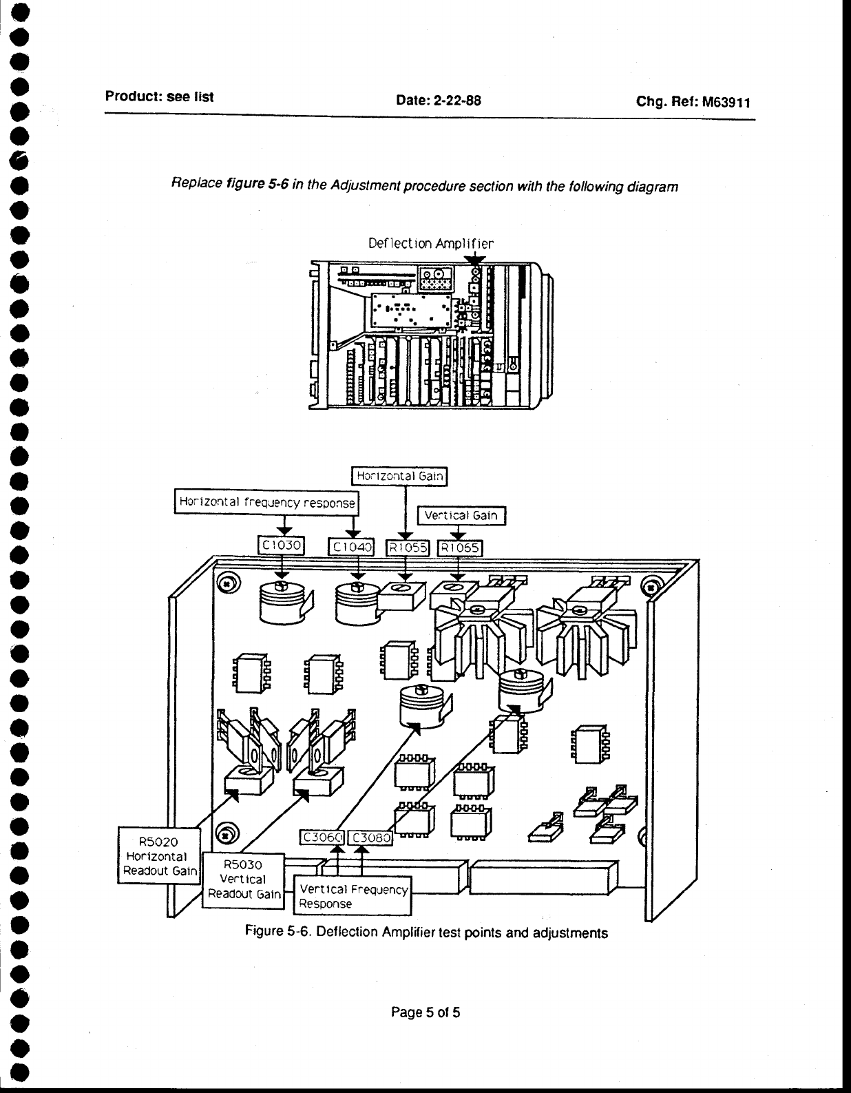
Product:
see
llst Chg.
Ref:
M63911
Replace
tigure 5-6 in the Adjustment procedure
section
with the following
diagram
Figure
5-6. Deflection
Amplifier
test
points
and adjustments
o
o
o
o
I
a
e
o
o
a
o
I
o
o
o
t
I
o
t
a
o
I
a
a
o
t
o
o
I
o
I
o
o
O
I
o
O
I
I
o
o
o
o
o
Def iectron
Arnplif
ier
Horl
Zontal
freqJency
response
Page
5 ol
5

o
o
O
a
a
a
t
a
o
o
o
o
o
o
o
I
a
a
o
I
I
a
o
o
o
t
o
o
I
,
t
o
o
o
a
o
o
o
:o
o
o
o
o
O
-^l-.r-- - r
teKtrontx,
Conmined to Erca$eno
Date:5-1G-Bg
Product:
See
List
ITIANUAL
CHANGE
INFORMATION
Ghange
Reference:
C2t5lgg
Manual
Part
No:
See
List product
Group: ZO
PERFORMANCE
CHECK
PROCEDURE
o
a
o
o
o
o
G
a
o
o
o
I
o
o
o
o
o
I
I
a
O
a
o
o
o
o
o
o
o
o
I
a
a
o
o
o
o
o
)
o
o
o
o
a
INSTRUMENT
49UP
Seruice
1
492P/6
Service
1
4941P
Service
t
4951P
Service
l
496/P
Service
I
492NAP
Service
1
492B|BP
Service
1
494NAP
Service
1
2753P
Service
1
27541P
Service
i
27551P
Service
t
2755NAP
Service
l
2756P
Service
1
MANUAL
070,3783-01
07a-4232-O0
070-4416-00
070-5084-00
070-3481-00
070-5565-01
070-5565-01
070-5560-00
070-6306-00
070-6097-00
070-6032-01
070-6032-01
070-6318-00
NOTE
Ih".n performing
lhe
accuracy
check
at 10
dB/Dlv
mode
on
some instrument
options,
the last
.t0
dB
step
of
Display
Dynamic
Range
may
not
appear
to meet
specification
when
the 10
KHz
Resolution
Bandwith
Filter
is
used'
This
is
observed.
as noise
inierrering
with
the
signal when
the External
Attenuator
is
set
to
g0
dB. The
signalwill
appear
too
high,
and
noise
can
6e
seen
on either
side. lf
this
is
the case,
then
change
the
sparvDiv
to 10
kHz'
the resoulution
Bandwidth
Filter
to 1
kHz,
and
the video
Fitter
to wlDE. Then
reset
the
External
Atlenuator
lo 0 dB,
readiust
the
signal
Generator
outpul
to FULL
scFEEN and retest
the 10
dB/Dlv
mode.
Page
1
ol 1

o
o
o
a
o
o
o
o
o
o
o
a
o
o
t
o
o
a
o
I
o
o
a
o
o
o
I
o
o
o
o
O
I
o
o
o
o
o
'O
o
o
o
a
a
Tektronix.
Cottrti.d to Ercrltono
Date:
$01€8
Product:
See list
MANUAL
CHANGE
INFORMATION
Change
Relerence:
M66071 Efi/SN 8010100
Manual
Parl
No:
See list produci
Group: 26
o
a
o
o
I
o
o
a
o
o
o
a
o
o
o
o
a
o
o
I
t
I
a
a
a
o
o
o
o
C
o
O
o
o
T
O
o
o
O
a
o
o
o
I
INSTBUMENT
494NAP Operators
49YP Operators
2753P Operators
27541P Operators
2756P Operators
4928/BP Operators
2755NAP Operators
PART
NO.
070-5557-01
070-5082-00
070-6305-00
070-6096-00
070-6317-00
070-5552-01
070-6031-01
070-5560-00
070-5084-00
070-6306-00
070-6097-00
070-6318-00
070-5565-01
070-6032-01
494A/AP
495/P
2753P
2754tP
2756P
4928/8P
2755NAP
Service
1
Service
1
Service
1
Service
t
Service
1
Service
1
Service
t
ADD:
oPTtoN
43
Option
43
provides
a reduced
graticule
ray
tube. This
option
atso
enables the main
disptay
readout
characters
to be
positioned
outside
the
grdicule
area.
Page
1
ot 1

o
o
o
o
e
o
e
o
o
t
o
I
t
o
o
I
I
a
a
I
t
o
I
O
I
o
o
o
o
o
o
o
o
o
a
I
o
o
o
o
o
o
o
a
Tekt"fp"n[X.
Date: 5/u9o
Product:
494N4g4Ap
Service
Vol. 1
MANUAL CHANGE INFORMATION
Change
Reference:
C2lSgO
ManualPart
No. 070-5s60-OO product Group: 2E
In
section
4 - PERF)RMANCE
)HECK pRocEDURE
change
step
r r as foltows:
Replace header secfian with the foltowing:
11.
Check
Resolution
Bandwidth
and
Shape
Factor
(bandwidth
is
within
2oo/o
ot
the
selected
Landwidth
for
all
butthe'l0
Hzfilter;
.10
Hzto 1
MHz
in
decade
steps,
and 3 MHz; shape factor is 7.5:.t
or less
_ 60 dB
bandwidth
for
the
.t0
Hz
filrer
is
s150
Hz)
Change step i. to read as follows:
.
i.
Repeat
the
process
to
check
the resolution
bandwidth
and
shape
lactor
for
the 10
kHz,
1
kHz,
and 100
Hz
fihers.
j.
To
checklhe60dB
bandwidth
of
the
1
0
Hzfitter,
setthe
SpanrDiv
ro 50 Hz, and the REFEHENCE
t_EVfL
lo _20
dBm.
Push
AUTO
RES,
VTDEO
FTLTER
WlOe, and ser
PEAK
AVERAGE
to average.
k.
Check
that
the
60
dB
bandwidth
is
<150
Hz.

o
o
o
O
o
o
t
o
o
a
o
a
o
o
o
I
o
o
o
t
o
o
C
o
o
o
o
o
o
t
o
o
t
o
t
a
o
o
o
o
I
o
o
I
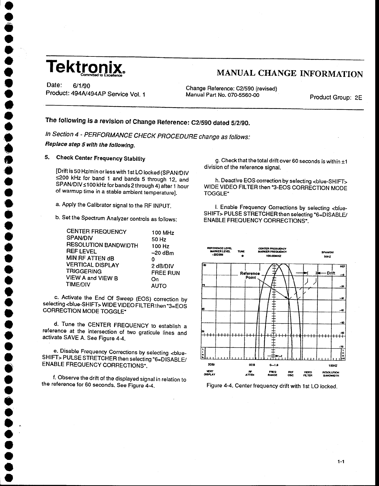
Tektfgnl;.
Date: 6/1190
Product:
494N494Ap
Service Vot.
1
MANUAL CHANGB INFORMATION
Change
Reference: CA59A
(revised)
ManualPart
No.070-5560-00 product
GrOup:
2E
o
o
C
o
O'
o
o
o
o
o
o
o
o
o
o
rf
a
I
o
t
o
o
o
a
o
o
o
o
I
t
t
I
I
o
o
I
C
I
a
o
I
o
I
o
The
followlng
is a revision
of change
Reference:
c2ls90
datect
slztgo.
ln section 4 - PERFORMANCE
cHEcK pRocEDIJRE change
as foilows:
Replace
step
5 wlth the
fottowlng.
5. Check
Center
Frequency
Stabitity
[Drift
is
50
Hzlmin
or
less
with
1 st
LO
locked
(SPAN/DtV
<200
kHz
for
band
1 and
bands
5 through
12,
and
SPAN/DlVs1
00kHzforbands2through
+)lfter
t hour
ol warmup
time
in
a
stable
ambient
temperature].
a.
Apply
the
Catibralor
signalro
the
RF tNpUT.
b.
Set
the
Spectrum
Analyzer
controls
as
{ollows:
g.
check that
the
total drift
over
60
seconds
is within
+1
division
of the reference
signal.
h.
Deactive EOS
conection
by
selecting
<blue-SHIFT>
WIDE
VIDEO
FILTER
then
B-EOS CORRECTTON
MODE
TOGGLE'
l. Enable
Frequency
Coneclions
by selecting
<blue-
SH
IFT>
PU LSE STRETCHER
the
n selecring
.6=D
TSABLE/
ENABLE
FREOUENCY
CORRECTIONS'.
CENTER
FREOUENCY
SPAN/DIV
RESOLUTION
BANDWIDTH
REF
LEVEL
MIN
RF
ATTEN
dB
VERTICAL
DISPLAY
TRIGGERING
VIEWA
and
VIEW
B
TIME/DIV
100
MHz
50
Hz
100
Hz
-20 dBm
0
2 dB/DIV
FREE
RUN
On
AUTO
F€Hc€|ffi
uilEntna, tw
-20ogr *
ffiREffi
IM(EN Ff,€q,€Td
t6,@rrE
G-lr
reo
asG
SPAW
frl
c. Aclivate
the End
Of Sweep (EOS)
correction
by
selecting
<blue-SHIFT>
WIDE
VIDEO
FtLTERrhen
"3=EOS
CORRECTION
MODE
TOGGLE.
d. Tune
rhe
CENTER
FREOUENCY
ro establish
a
reference
at the intersection
of two graticule
lines
and
activate
SAVE
A. See
Figure
4-4.
SHIFT>
PULSE
STRETCHER
rhen
seleciing
"6=D|SABLE/
ENABLE
FREOUENCY
CORRECTIONS".
f. Observe
the
drift
of the
displayed
signal
in
relation
to
the relerence
for
60
seconds.
See
Figure
4_4.
ODB
*
Alm
20&
GF
O3RAY E
G
tmta
vD@ &|Jm
fLE WA
Figure
4-4.
Center
frequenry
drift
wilh 1st
LO locked.
en' tl 1""
.- Drift
:\ I
),
'/N l/ -T
4
I
5{
tl f
,+,-,"1,
I| | tl t;
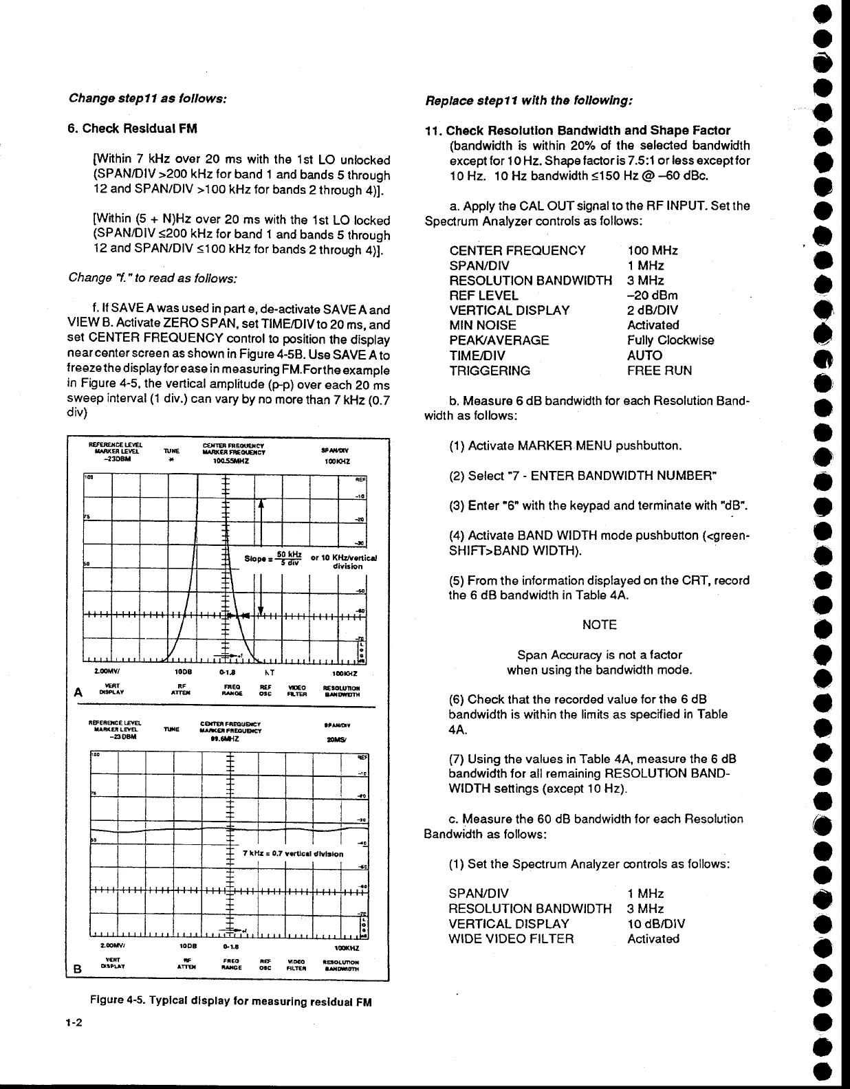
Change
stepll as follows:
6. Check
Reslduat FM
[Within
7 kHz over
20 ms
with the 1st
LO unlocked
(SPAN/DIV
>200 kHz for
band
1 and
bands
5 rhrough
12
and SPAN/DIV
>100
kHz for bands
2 rhrough
4)1.
[Within
(5
+ N)Hz
over
20 ms with
rhe
1st
LO locked
(SPAN/DIV
s200 kHz
for band
1
and bands
5lhrough
12
and SPANiDIV
<100
kHz tor
bands
2 rhrough
4)1.
Change
'f-"
to read
as follows:
f, ll SAVE
A
was
used
in
part
e, de-activate
SAVE
A and
VIEW
B.
Activate
ZERO SPAN,
set
TIME/DIV
ro
20
ms,
and
set
CENTER
FREQUENCY
control
to
posirion
the display
nearcenterscreen
as shown
in Figure
4-5B.
Use SAVEAto
f reeze
the
display
for ease in
measuring
FM.Forthe
example
in
Figure
4-5,
the vertical
amplitude (gp)
over
each
20
ms
sweep
inleryal
(1
div.)
can
vary
by no
more
th an7
kHz
(O-7
div)
Replaee stepl7 wtth the tollowlng:
11.
Check Resolutlon Bandwldlh
and
Shape Factor
(bandwidlh
is within 2O%
ot lhe selected bandwidth
except for 10 Hz. Shape
factor is 7.5:1
or
less
exceptlor
1
0 Hz. 1 0 Hz bandwidth <150
Hz
@
-60 dBc.
a.
Apply the
CAL
OUT signalto the RF
INPUT. Set the
Spec{rum Analyzer
controls as
follows:
CENTER
FREOUENCY
SPAN/DIV
RESOLUTION BANDWIDTH
REF LEVEL
VEHTICAL
DISPLAY
MIN NOISE
PEAI(AVERAGE
TIME/DIV
TRIGGERING
'lO0
MHz
l MHz
3 MHz
-20
dBm
2
dB/DIV
Activated
Fully
Clockwise
AUTO
FREE RUN
o
o
3
o
o
o
t
)
o
O
I
a
o
)
o
o
o
I
o
a
o
t
o
o
o
o
o
o
e
I
o
t
I
o
o
t
C
a
a
o
o
o
a
o
b. Measure 6 dB bandwidth
for each
Resolulion Band-
width
as follows:
(1)
Activate MARKER
MENU
pushbutton.
(2)
Select'7 - ENTER BANDWIDTH
NUMBER"
(3)
Enter
"6"
with the keypad
and terminate with
"dB'.
(4)
Activate BAND WIDTH mode
pushbutton
(<green-
sHtFT>BAND WTDTH).
(5)
From the inlormation
displayed on lhe CRT, record
the 6 dB bandwidth in Table 44.
NOTE
Span Arcurary is not a lactor
when using
the bandwidth
mode.
(6)
Check that the recorded value for the 6 dB
bandwidth is within the limits as specified in Table
44.
(7)
Using the values in Table
4A, measure the 6 dB
bandwidlh
lor all
remaining
RESOLUTION
BAND-
WIDTH settings
(except
10 Hz).
c. Measure
the 60 dB bandwidth for each Resolution
Bandwidth as follows:
(1
) Set the Spectrum Analyzer controls
as
follows:
SPAN/DIV l MHz
RESOLUTION
BANDWIDTH 3 MHz
VERTICAL DISPLAY 1O
dBIDIV
WIDE VIDEO FILTER Activated
nEfg* cv€!
IegEE
-2308M UG c€,frE; mEqrcrw
Kqft€d
roos!il||}tz
2-6ilv/
A rHI'
10DS
RF
lru
ol,8 t T looxHz
E€O ET ru€O ftEruM
uc 6C AB 3Ailm
aE€n&€wR
udiltryR
-aD8rl
CffiFBEU*Y
r*sn&uw
ar.6aaJz
atMr
a,|tg
e6ra/,
ffi
B dttut
IODB
A1E Fico iF sEo ts!@i
asE olc FLE| tailfr
Sror =-9!$ or to Ktkrvrnicd
G
tttl
7 tHr:0.7 verucrt
dlvlJon
ttll
't
a
Flgure 4-5.
Typlcal dlsptay for measurlng
resldual
FM
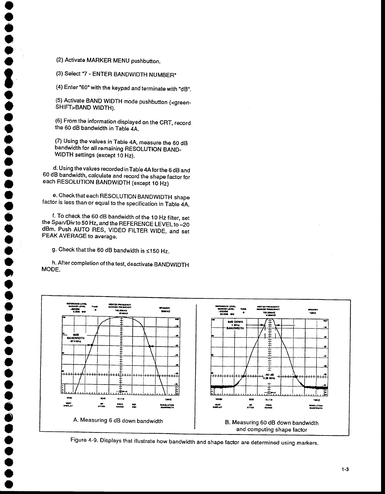
(2)
Acrivare
MARKER
MENU pushbutton.
(3)
Select "7 - ENTER
BANDWTDTH
NUMBER"
(4)
Enter'60" with
the
keypad
and
terminate
wilh "d8".
(5)
Activate
BAND
WIDTH
mode pushbutton
(<green_
sHIFT>BAND
WTDTH).
(6)
From
the
information
displayed
on
the CRT,
record
the 60
dB
bandwidth
in
Tabte
4A.
(7)
Using
the values
in
Table
44, measure
the 60 dB
bandwidrh
for allremaining
RESOLUTION
BAND-
WIDTH
setrings (excepr
10
Hz).
d.
Using
the values
recorded
in
Table
44forthe 6
dB
and
60
dB bandwidth,
calculate
and
record
the
shape
factor
for
each RESOLUTTON
BANDWTDTH
(excepr
10
Hz)
e.
Check
that
each
FiESOLUTION
BANDWTDTH
shape
factor
is less
than
or equal
to lhe
specification
in
Table
4A.
f.
To check
the 6O
dB bandwidth
of
the 1O
Hz filter,
set
the
Span/Div
lo 50
Hz,
and
the
REFERENCE
LEVEL
to
_20
dBm. Push
AUTO RES,
VTDEO
FILTER
WIDE,
and ser
PEAK
AVERAGE
to average.
g. Check
lhat
the 60 dB bandwidth
is
s150 Hz.
h.
Aftercompletion
of
thetest,
deactivate
BANDWIDTH
MODE.
3B
v
fxmfiofl t
t?. Hr I\
/\
...L
I/
EgH|.tE q'E*ffi
uq|.E 'E reiu|d
?j; * * ''f,& re
&e|'lt ffu'[ffi
KUf,! tE re@
# - ' '-aHE !E
tt aN Ert
Fff:cE
lnqM*
s Fl!
^fru
IE
A. Measuring
6 dB
down
bandwidth B. Measuring
6O
dB down
bandwidth
and computing
shape
factor
.dA FTYN
t I{r /+\
)r{ + \+
/;+
i\
+
I
I!
/
I
,!{d ,
''a-6xw '
-{-
L.,.
.{ \
it.. .:=!ry -E
Figure
4-9.
Displays
that
illustrate
how
bandwidth
and
shape factor
are determined
using
markers.
1-3
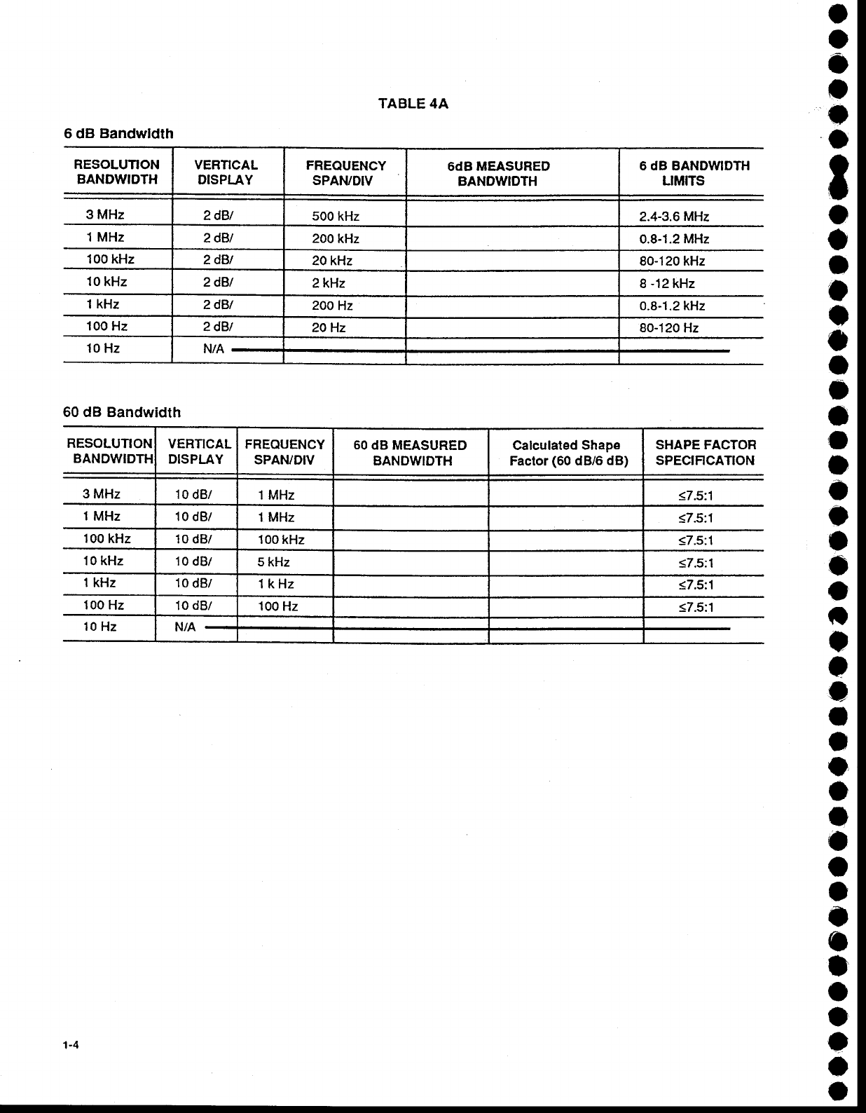
RESOLUTION
BANDWIDTH
3 MHz
1 MHz
6 dB BANDWIDTH
LIMITS
60 dB Bandwidth
RESOLUTION
BANDWIDTH VERNCAL
DISPLAY FREOUENCY
SPAIVDIV 60
dB MEASURED
BANDWIDTH Caleulated
Shape
Factor (60 dB/6 dB) SHAPE FACTOR
SPECIFICATION
3 MHz 10
dB/ l MHz <7.5:1
1
MHz 10 dB/ 1 MHz <7.5:1
100
kHz 10 dB/ 100
kHz <7.5:1
'10
kHz t0 dB/ 5
kHz <7.5:1
1
kHz 10
dB/ lkHz <7.5:1
100
Hz 10
dB/ 100
Hz <7.5:1
10
Hz N/A
o
o
a
a
o
t
t
-
-
o
t
o
t0
I
o
a
o
o
I
o
a
C
a
o
C
I
o
t
a
I
a
I
a
o
a
t
a
o
'a
a
a
o
a
I
t
Change
step 12
as follows:
12. Check
Calibrator
Output
(-20
dBm
r0.g
dB)
a. Apply
an
external
100
MHz
signal
to
lhe
power
meter
through
a
3 dB
attenualor
and
a
50e
iable.
Set
the generaror
output
level
lor
a
reading
ol
-20 dBm
on the
power
meter.
Change
step l7 as follows:
PART
I
Change'a."
ta read
as follows:
a.
Connecl
the test
equipment
as
shown
in
Figure
4_14.
Set
the
Spectrum
Analyzer
controls
as
follows:
'Selea 3 test frequencies
Test Freq.
1: 1O
kHz
- 1.8
GHz
Tesl
Freq.
2: 1.8-18
GHz
Test
Freq.
3: 18-21
GHz
PARTIII
Change "b."
to read as follows:
b.
Connect
the test
equipment
as
shown
in
Figure
4-15.
Set
the Spectrum
Analyzer
controls
as
{ollows:
VERTICAL
DISPLAY
NARROW
VIDEO
FILTER
TIME/DIV
PEAI(AVERAGE
VIEW
A and VIEW
B
CENTER
FREOUENCY
SPAN/DIV
RESOLUTION
BANDWDITH
REF LEVEL
MIN RF
ATTEN
dB
MIN
NOISE
VEBTICAL
DISPLAY
NARROW
VIDEO
FILTER
TIME/DIV
PEAIOAVERAGE
VIEW
A and VIEW
B
2dBtDtv
On
AUTO
Fully
Clockwise
On
Test
Frequency*
200
kHz
1
MHz
-25 dBm
50
On
2 dB/DtV
On
AUTO
Fully
Clockwise
On
'SeleA
3 test
lrequencies
Test
Freq. 1
: 1O
kHz
-
1.8
GHz
Test
Freq.2: 1.8-18
GHz
Test
Freq.3; 1g-21
GHz
PARTIT
Change'b."
to read
as
follows:
b.
Connect
the
test
equipment
as
shown
in
Figure
4-14.
Set
the
Spectrum
Analyzer
controls
as
follows:
'Select
3
test
frequencies
Test
Freq-
1 : 10 kHz
- 1 _8 GHz
Test
Freq. 2: 1.8-18 GHz
Test
Freq.3: 't8-21
GHz
CENTER
FREOUENCY
SPAN/DIV
RESOLUTION
BANDWDITH
REF
LEVEL
MtN
RF
ATTEN
dB
MIN
NOISE
VERTICAL
DISPLAY
NARROW
VIDEO
FILTER
TIME/DIV
PEAIVAVERAGE
VIEW
A and
VIEW
B
CENTER
FREOUENCY
SPAN/DIV
RESOLUTION
BANDWDITH
REF
LEVEL
MIN
RF
ATTEN
dB
MIN
NOISE
Tesl
Frequenry'
200
kHz
100
kHz
-30
dBm
0
On
2 dB/DIV
On
AUTO
Fully
Clockwise
On
Test
Frequency'
200 kHz
1
00 kHz
-25 dBm
30
On
1-5
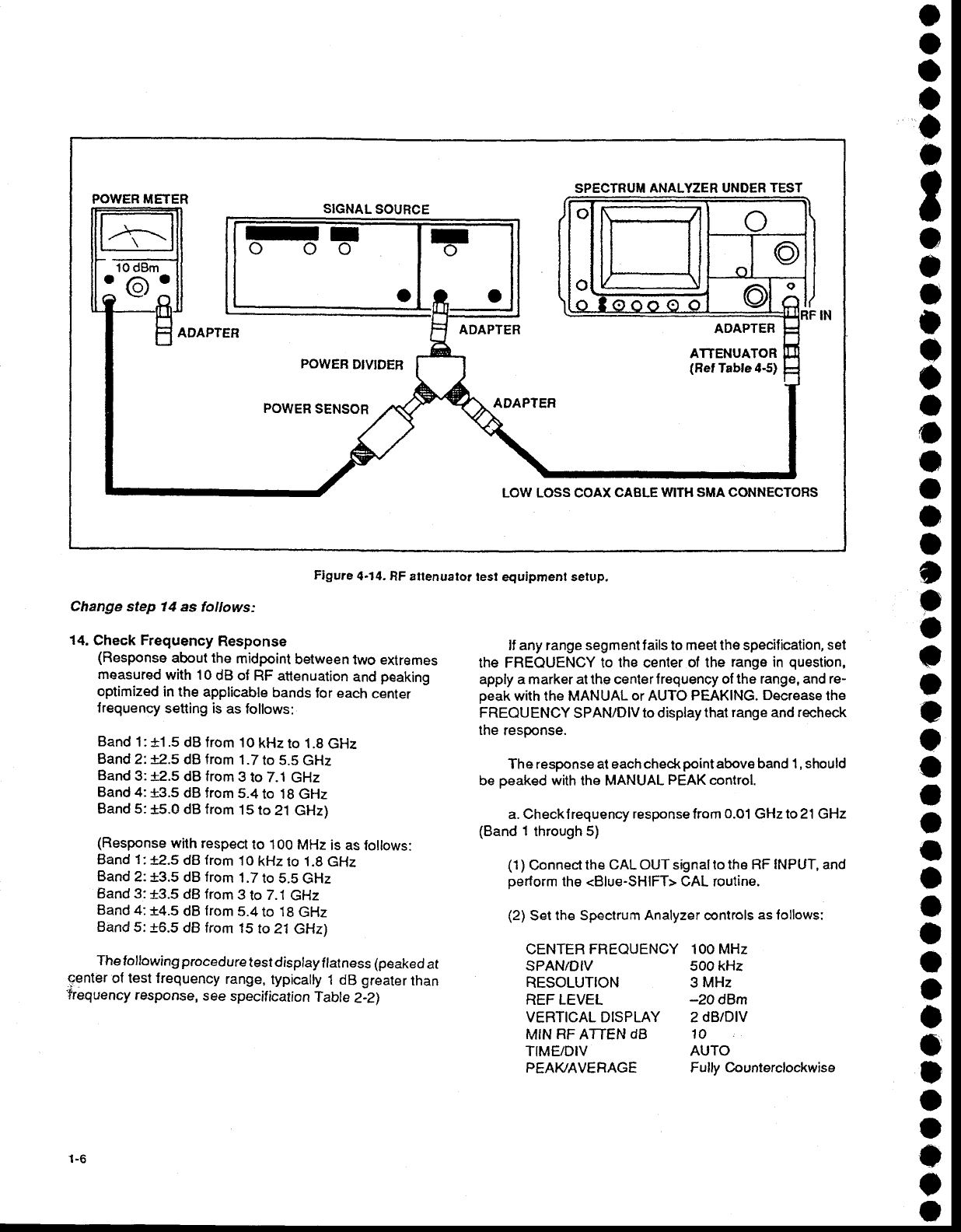
o
a
o
o
a
o
^
r
J
o
I
t
I
o
o
a
o
o
o
o
I
,
o
I
o
t
o
o
o
a
a
a
I
a
I
o
I
I
o
I
t
t
o
I
t
Figure 4.14.
RF attenuator test equipment setup,
Change step 14 as follows:
14.
Check Frequency Response
(Response
about the midpoint
between
lwo exlremes
measured
with 10
dB of RF attenuation
and
peaking
optimized
in the applicable
bands
for each
cenrer
lreguency
setting is as lollows:
Band
1:
+1
.5 dB
from 10
kHz to 1.8
GHz
Band
2'.
r2.5 dB from
1.71o
5.5
GHz
Band
3:
f2.5 dB from
3 to 7.i GHz
Band 4:
+3.5
dB from
5.4
to 18 GHz
Band 5:
+5.0
dB from
15 to 21 GHz)
(Response
with respect
to 1OO
MHz is as
follows:
Band
1
:
.t2.5
dB from I
O
kHz
to 1
.8 GHz
Band
2:
+3.5
dB
from
1.7
to 5.5
GHz
Band 3:13.5 dB from
3 to 7.1
GHz
Band 4:14.5 dB from
5.4
to 18
GHz
Band
5: +6.5
dB from 't5
to 21 GHz)
The
folfowing
procedure
test display
flatness
(peaked
at
center
of test frequency
range,
typically
1 dB greater
than
Trequency
response,
see specification
Table
2-2)
lf any range
segment
f
ails
to
meet the
specif
ication,
set
the FREOUENCY to the center
of the range in question,
apply a marker
at the center f requency of
the range, and re-
peak
with
the MANUAL
or AUTO
PEAKING.
Decrease
lhe
FREOUENCY SPAN/DlV
to display that
range
and
recheck
the response.
The response at each check
point
above band 1
,
should
be peaked
with
the MANUAL
PEAK
control.
a. Checklrequency
responsefrom
0.01
GHzto 21 GHz
(Band
1
through
5)
{1)
Connecl
the
CAL
OUT signal
to the RF
INPUT,
and
perform
the <Blue-SHIFT> CAL routine.
(2)
Set
the
Spectrum
Analyzer controls
as
lollows:
CENTER FREOUENCY
100MHz
SPAN/DIV 500 kHz
RESOLUTION 3 MHz
REFLEVEL -20d9m
VERTICAL
DISPLAY 2
dB/DIV
MIN
RF
ATTEN
dB 10
TIME/DIV AUTO
SPECTRUM
ANALYZER UNDER TEST
POWER METER SIGNAL
SOURCE
ADAPTEF ADAPTER
POWEB
DIVIDEB
POWER
SENSOR ADAPTEF
LOW LOSS COAX CABLE
WITH SMA CONNECTORS
1-6
PEA}VAVERAGE Fully
Counterclockwise
Tercfgnix MANUAL
cHANcE
INFoRMAnoN
CETvitTTEDToEcEu.E^pE Date: l1_Sep_gl
Product: See
List
.
Change
Reference: C1-991
Manual
Part
No.: See Lisl
DESCRIPTION Prodrrct
Group
2E
o
o
o
o
o
o
?
I
o
a
o
t
o
o
o
o
t
t
o
o
o
O
o
o
o
o
o
a
o
J
I
a
o
o
)
a
o
O
a
a
O
a
o
o
Effective
for
Alt
Sertal
Numbers:
070-7556-00,
Service Votume
1
070-5560-00,
Service Volume
1
070-5084-00,
Service Votume
1
070-7679-00,
Service
Volume
1
070-6306-00,
Service Volume
1
070-6097-00,
Service
Votume
1
070-6032-01,
Service
Volume
1
070-6032-01,
Service Votume
1
070-6318-00,
Service
Volume
1
Make
the
fotlowlng
changes
In
your
Servtce
Volume
i manuat:
Section
2
- Specification
Change
the
1
dB
Compression
specificafion
as
shown
below.
Section
4
- performance
Verification
Add
the
toilowing
equipment
to
the
Equipment
Required
tabre.
Power
Sptitter
(Femate
SMA
Connectors)
20
dB
Attenuator
(SMA
Connec_
tors)
492PGM
494NAP
495/P
497P
2753tP
2754tP
2755tP
2755NAP
2756P
TEKTRONIX
Part
No.
015-0565-00
(1
dB
Compression
check).
TEKTRONIX
Part
No.
015-1003-00
(1
dB
Compression
check).
,,t
i :i;lv
:,;
Check
1
dB
Compression
point
0
dBm
in
MIN
NOTSE
mode for
Bands
1
through
5.
a. Connect
the
test
equipment
as
shown
in
the followirq
figure.
Measured
in
Min
Noise
nrode
with
no
RF
attenution.
Replace
the
1
dB
compression
Point
performance
verification procedure
with
the
following procedurg;
Page 1 ot 2
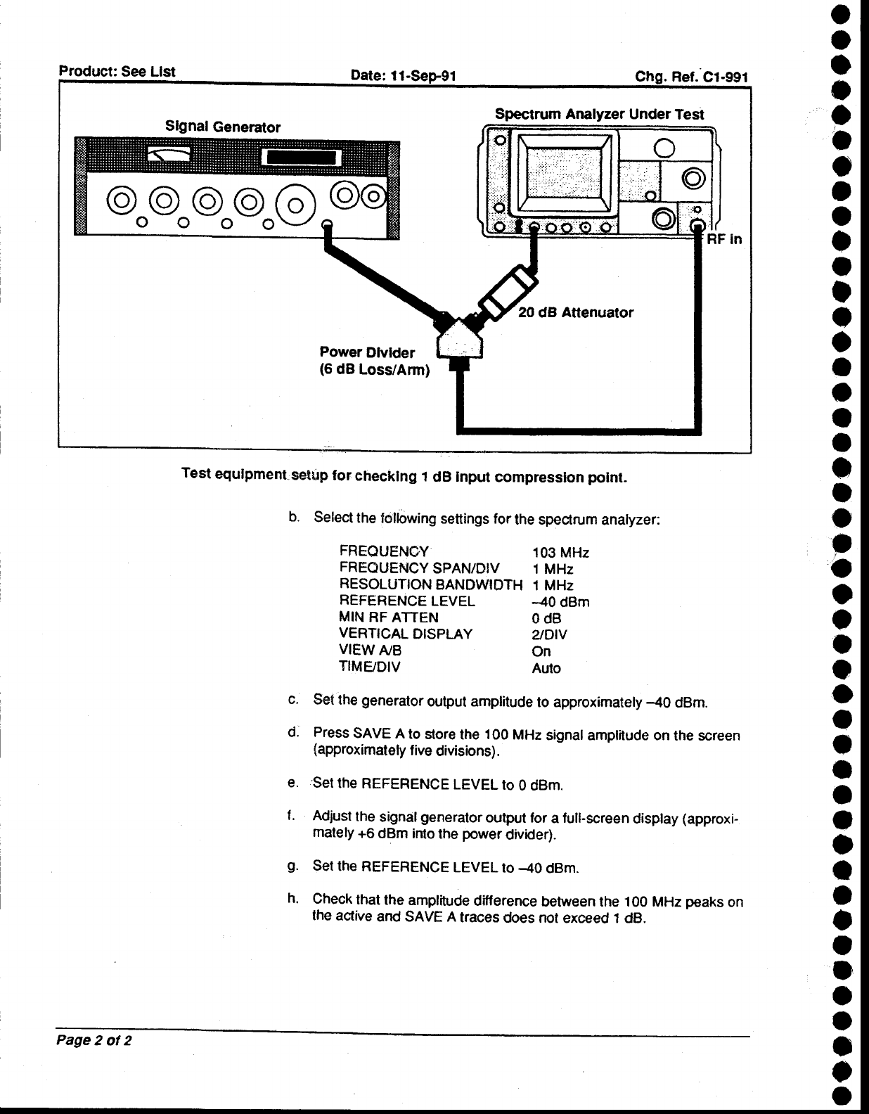
Product:
See Llst Date:
11 Ref.
C1-991
Spectrum Analyzer
Under
Test
Test
equlpment,setup
lor checklng
I dB lnput
compresslon
polnt-
b. Sefect
lhe following
settings
for
the specirum
anatyzer:
FBEQUENOY 103
MHz
FREQUENCY
SPAN/DIV 1 MHz
RESOLUTION
BANDWTDTH
1 MHz
a
o
o
o
o
o
o
I
o
o
I
I
o
O
I
a
a
a
t
o
o
I
o
o
o
O
t
o
o
o
I
o
o
a
a
I
a
I
I
o
o
I
t
o
c.
d.
g.
h.
e.
f.
-40 dBm
0dB
REFERENCE
LEVEL
MIN
RF
ATTEN
VERTICAL
DISPLAY aIDIV
VIEW
A/B On
TIME/DIV AuTo
set the
generator
output amplitude
to approximatety
-40 dBm.
Press
SAVE
A
to store
the
100
MHz
signal amplitude on
the screen
{approximately
f ive
divisions).
.Set
|he
REFERENCE
LEVEL
to
O dBm.
Adiust
lhe
signal
generator
output for
a
full-screen
display
(approxi-
mately
+6
dBm into
the
power
divkler).
Set
the
REFERENCE
LEVEL
to
-40 dBm.
Check
that
the amplitude
ditlerence
between the 100
MHz
peaks
on
the
active
and SAVE A traces
does not
exceed 1 dB.
Page 2 of 2
o
a
a
o
a
o
o
I
O
a
()
)
t
o
o
o
c
I
o
o
o
o
o
t
o
a
t
o
o
I
a
a
o
o
a
o
o
o
o
o
o
o
o
o

o
o
t
o
I
a
a
a
o
I
o
I
e
o
o
t
I
J
t
|}
o
o
o
e
?
o
o
t
e
o
t
I
o
o
I
a
a
o
t
o
a
o
;
o
