Telecom Design TD1508 TD1508 SIGFOX Modem for ITU Region 2 User Manual TD1508 Datasheet rev1 4
Telecom Design S.A. TD1508 SIGFOX Modem for ITU Region 2 TD1508 Datasheet rev1 4
User manual
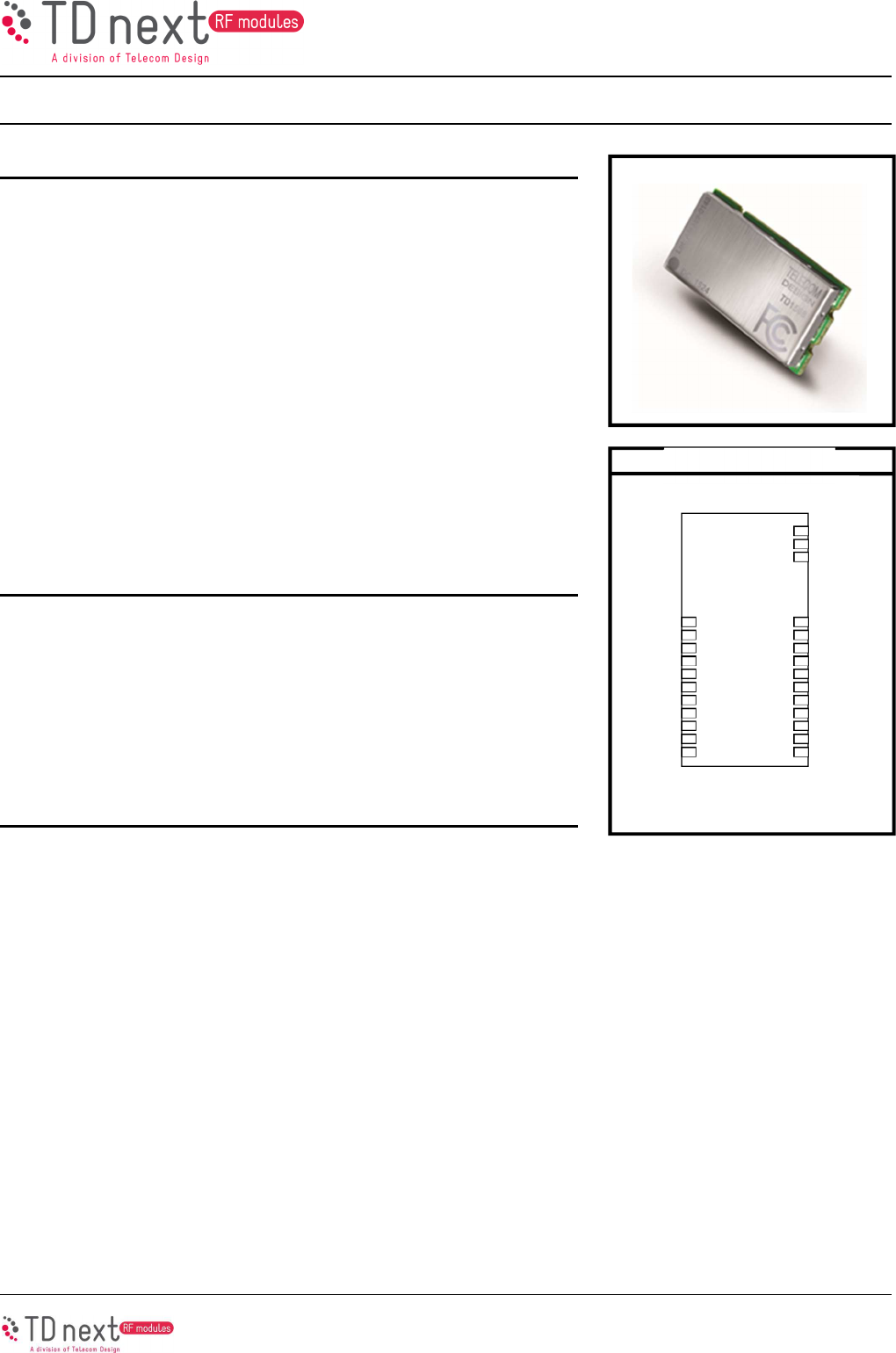
TD1508
Rev 1.4 (07/16) 1
H
IGH
-P
ERFORMANCE
,
L
OW
-C
URRENT
US
SIGFOX™
G
ATEWAY
Features
SIGFOX Ready™
Frequency range = ITU Region 2 ISM Band (Americas, 902~928 MHz)
Receive sensitivity =-127 dBm
Modulation
•
(G)FSK, 4(G)FSK, GMSK
•
OOK
Max output power
•
+24 dBm
Low active radio power consumption
•
21 mA RX
•
230 mA TX @ +23 dBm
Power supply = 2.3 to 3.6 V
LGA25 (25.4×12.7×3.81mm, 1”×0.5”×0.15”) Land Grid Array package
Available in several conditioning methods
Applications
SIGFOX™ transceiver (fully certified)
Sensor network
Health monitors
Remote control
Home security and alarm
Telemetry
Industrial control
Description
TD next’s TD1508 devices are high performance, low current SIGFOX™
gateways. The combination of a powerful radio transceiver and a state-of-the-
art ARM Cortex M3 baseband processor achieves extremely high performance
while maintaining ultra-low active and standby current consumption. The
TD1508 device offers an outstanding RF sensitivity of -127 dBm while
providing an exceptional output power of up to +23 dBm with unmatched TX
efficiency. The TD1508 device versatility provides the gateway function from a
local Narrow Band ISM network to the long-distance Ultra Narrow Band
SIGFOX™ network at no additional cost. The broad range of analog and digital
interfaces available in the TD1508 module allows any application to
interconnect easily to the SIGFOX™ network. The LVTTL low-energy UART,
the I
2
C and SPI buses, the multiple timers with pulse count input/quadrature
decoding/PWM output capabilities, the high-resolution/high-speed ADC and
DAC, along with the numerous GPIOs can control any kind of external sensors
or activators. Featuring an AES encryption engine and a DMA controller, the
powerful 32-bit ARM Cortex-M3 baseband processor can implement highly
complex and secure protocols in an efficient environmental and very low
consumption way.
Patents pending
Pin Assignments
2
1
4
3
6
5
8
7
10
9
11
2
1
22
19
20
17
18
15
16
13
14
12
2
4
25
23
GND
GND
Reserved
USR4
DB3
DB2
SDA
SCL
VDD
USR2
GND
GND
USR3
RST
DAC0
USR0
USR1
TX
RX
ADC0
TIM2
GND
RF_GND
RF
RF_GND

TD1508
2 Rev 1.4 (07/16)
Disclaimer: The information in this document is provided in connection with Telecom Design products. No license,
express or implied, by estoppel or otherwise, to any intellectual property right is granted by this document or in
connection with the sale of Telecom Design products.
TELECOM DESIGN ASSUMES NO LIABILITY WHATSOEVER AND DISCLAIMS ANY EXPRESS, IMPLIED OR
STATUTORY WARRANTY RELATING TO ITS PRODUCTS INCLUDING, BUT NOT LIMITED TO, THE IMPLIED
WARRANTY OF MERCHANTABILITY, FITNESS FOR A PARTICULAR PURPOSE, OR NON-INFRINGEMENT.
IN NO EVENT SHALL TELECOM DESIGN BE LIABLE FOR ANY DIRECT, INDIRECT, CONSEQUENTIAL,
PUNITIVE, SPECIAL OR INCIDENTAL DAMAGES (INCLUDING, WITHOUT LIMITATION, DAMAGES FOR LOSS
OF PROFITS, BUSINESS INTERRUPTION, OR LOSS OF INFORMATION) ARISING OUT OF THE USE OR
INABILITY TO USE THIS DOCUMENT, EVEN IF TELECOM DESIGN HAS BEEN ADVISED OF THE POSSIBILITY
OF SUCH DAMAGES.
Telecom Design makes no representations or warranties with respect to the accuracy or completeness of the
contents of this document and reserves the right to make changes to specifications and product descriptions at any
time without notice. Telecom Design does not make any commitment to update the information contained herein.
Unless specifically provided otherwise, Telecom Design products are not suitable for, and shall not be used in,
automotive applications. Telecom Design products are not intended, authorized, or warranted for use as
components in applications intended to support or sustain life.
© 2015-2016 Telecom Design S.A. All rights reserved. Telecom Design®, logo and combinations thereof, are
registered trademarks of Telecom Design S.A. SIGFOX™ is a trademark of SigFox S.A. ARM®, the ARM Powered®
logo and others are the registered trademarks or trademarks of ARM Ltd. I2C™ is a trademark of Koninklijke Philips
Electronics NV. Other terms and product names may be trademarks of others.
TD1508
Rev 1.4 (07/16) 3
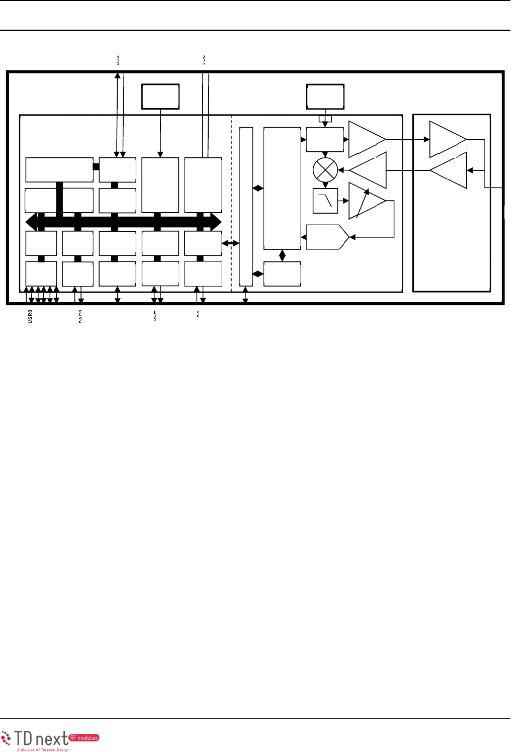
Functional Block Diagram
DB2
DB3
VDD
GND
TD1508
MCU / RF
Debug
I/F
ARM Cortex-M3
CPU
2x I2C
GPIO Timer
X4
DAC
32
-
bit Bus
2x
USART
INT ADC AES
Watch
dog
Flash
128K
B
RAM
32KB
Clock
Mgt
Energy
Mgt
DMA
Ctrl
LNA
PA
Logic
I
n
t
e
r
f
a
c
e
ADC
Frac-N
PLL
USR0
USR1
USR2
USR3
USR4
RST
DAC0
ADC0
TIM2
SDA
SCL
RX
TX
26 MHz
TCXO
32 kHz
XTAL
Reserved
MODEM
FIFO
Packet
Handler
2x
LowPo
w UART
RF
RF GND
RF
Front
End
LNA
PA

TD1508
4 Rev 1.4 (07/16)
T
ABLE OF
C
ONTENTS
Section Page
1
Electrical Specifications ................................................................................................... 6
1.1
Definition of Test Conditions ................................................................................................................. 15
2
Functional Description .................................................................................................... 16
3
Module Interface .............................................................................................................. 18
3.1
Low-Power UART (Universal Asynchronous Receiver/Transmitter) ................................................. 18
3.2
USART (Universal Synchronous/Asynchronous Receiver/Transmitter) .......................................... 18
3.3
I
2
C bus ...................................................................................................................................................... 18
3.4
Timer/Counter ......................................................................................................................................... 19
3.5
ADC (Analog to Digital Converter) ........................................................................................................ 19
3.6
DAC (Digital to Analog Converter) ........................................................................................................ 19
3.7
GPIO (General Purpose Input/Output) .................................................................................................. 20
3.8
RST (Reset) .............................................................................................................................................. 20
3.9
Debug ....................................................................................................................................................... 20
3.10
RF Antenna .............................................................................................................................................. 20
3.11
VDD & GND .............................................................................................................................................. 20
4
Bootloader ........................................................................................................................ 21
5
Pin Descriptions .............................................................................................................. 22
6
I/O alternate functionalities ............................................................................................. 24
7
Ordering Information ....................................................................................................... 26
8
Package Outline ............................................................................................................... 27
9
PCB Land Pattern ............................................................................................................ 28
10
Soldering Information ..................................................................................................... 29
10.1
Solder Stencil .......................................................................................................................................... 29
10.2
Reflow soldering profile ......................................................................................................................... 29
11
Board Mounting Recommendation ................................................................................ 30
11.1
Electrical Environment ........................................................................................................................... 30
11.2
Power Supply Decoupling ..................................................................................................................... 30
11.3
RF Layout Considerations ..................................................................................................................... 30
11.4
Host Antenna Circuit Trace Design ...................................................................................................... 30
12
Conformity Assessment Issues / FCC Regulatory Notices ......................................... 35
12.1
Modification Statement .......................................................................................................................... 35
12.2
Interference Statement ........................................................................................................................... 35

TD1508
Rev 1.4 (07/16) 5
12.3
Wireless Notice ....................................................................................................................................... 35
12.4
FCC Class B Digital Device Notice........................................................................................................ 35
12.5
Labelling Requirements for the Host Device ....................................................................................... 35
TD1508
6 Rev 1.4 (07/16)
1 Electrical Specifications
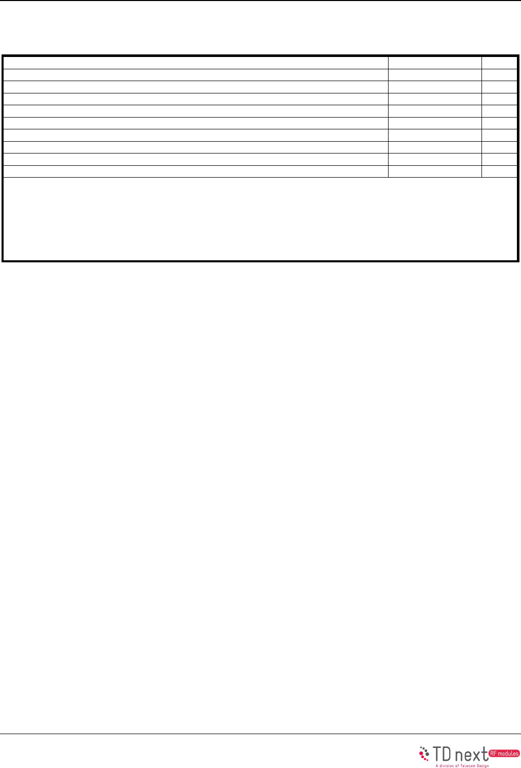
Table 1. Absolute Maximum Ratings
Parameter
Value
Units
V
DD
to GND 0 to +3.6 V
Instantaneous V
RF-peak
to GND on RF Pin -0.3 to +8.0 V
Sustained V
RF-peak
to GND on RF Pin -0.3 to +6.5 V
Voltage on Digital Inputs 0 to V
DD
V
Voltage on Analog Inputs 0 to V
DD
V
RX Input Power +10 dBm
Operating Ambient Temperature Range T
A
-30 to +75 °C
Storage Temperature Range T
STG
–40 to +125 °C
Maximum soldering Temperature 260 °C
Note:
Stresses beyond those listed under “Absolute Maximum Ratings” may cause permanent damage to the device.
These are stress ratings only and functional operation of the device at or beyond these ratings in the operational
sections of the specifications is not implied. Exposure to absolute maximum rating conditions for extended
periods may affect device reliability. Power Amplifier may be damaged if switched on without proper load or
termination connected. TX matching network design will influence TX V
RF-peak
on RF pin. Caution: ESD sensitive
device.

TD1508
Rev 1.4 (07/16) 7
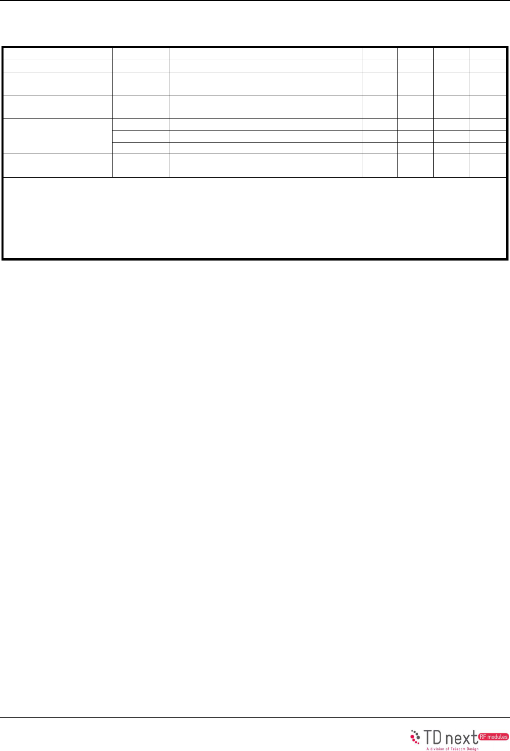
Table 2- DC Power Supply Characteristics
1
Parameter
Symbol
Conditions
Min
Typ
Max
Units
Supply Voltage
Range
2
V
DD
2.3 3.0 3.6 V
Power Saving Mode
2
I
Sleep
Sleep current using the 32 kHz crystal
@ 25°C 1.5 1.8 3.5 µA
Active CPU Mode I
Active
CPU performing active loop @ 14 MHz 2.55 3.0 3.45 mA
Active CPU Mode +
RX Mode Current
2
I
RX
— 13 16 mA
Active CPU Mode +
TX Mode Current
2
I
TX_+24
+24 dBm output power, 902.8 MHz, 3.3 V — 240 — mA
I
TX_+23
+23 dBm output power, 902.8 MHz, 3.3 V — 230 — mA
I
TX_+22
+22 dBm output power, 902.8 MHz, 3.3 V — 200 — mA
I
TX_+20
+20 dBm output power, 902.8 MHz, 3.3 V — 180 — mA
I
TX_+15
+15 dBm output power, 902.8 MHz, 3.3 V — 135 — mA
No
tes:
1. All specifications guaranteed by production test unless otherwise noted. Production test conditions and max
limits are listed in the “Production Test Conditions” section in “1.1. Definition of Test Conditions” on page 5.
2. Guaranteed by qualification. Qualification test conditions are listed in the “Qualification Test Conditions”
section in “1.1. Definition of Test Conditions” on page 14.
TD1508
8 Rev 1.4 (07/16)
Table 3. Transmitter RF Characteristics
1
Parameter
Symbol
Conditions
Min
Typ
Max
Units
TX Frequency Range
2
F
TX
902.0
— 928 MHz
Modulation Deviation
Range
3
∆f 902.0-928.0 MHz — 1.5 — MHz
Modulation Deviation
Resolution
3
F
RES
902.0-928.0 MHz — 28.6 — Hz
Frequency Error
2
F
ERR_25
902.0-928.0 MHz, 25°C, 3.3 V — ±2 — kHz
F
ERR_M20
902.0-928.0 MHz, -20°C, 3.3 V — ±3 — kHz
F
ERR_55
902.0-928.0 MHz, 55°C, 3.3 V — ±3 — kHz
Average Conducted
Power
2
P
AVCDP
-20°C to 55°C, 902.0-928.0 MHz, 3.3 V — — +25 dBm
Notes:
3. All specifications guaranteed by production test unless otherwise noted. Production test conditions and
max limits are listed in the “Production Test Conditions” section of “1.1. Definition of Test Conditions” on
page 5.
4. Guaranteed by qualification. Qualification test conditions are listed in the “Qualification Test Conditions”
section in “1.1. Definition of Test Conditions” on page 14.
5. Guaranteed by component specification.

TD1508
Rev 1.4 (07/16) 9
Table 4. Receiver RF Characteristics
1
Parameter
Symbol
Conditions
Min
Typ
Max
Units
RX Frequency Range
2
F
RX
902.0
— 928.0
MHz
Synthesizer
Frequency
Resolution
3
F
RES
902.0-928.0 MHz — 28.6 — Hz
Blocking
2,4
1M
BLOCK
Frequency offset ± 1 MHz, 902.0-928.0
MHz, 25°C, 3.3 V — -79 -68 dB
8M
BLOCK
Frequency offset ± 10 MHz, 902.0-928.0
MHz, 25°C, 3.3 V — -86 -75 dB
Spurious Emissions
2
P
OB_RX1
From 9 kHz to 1 GHz, 902.0-928.0 MHz,
25°C, 3.3 V — -84 — dBm
P
OB_RX2
From 1 GHz to 6 GHz, 902.0-928.0
MHz, 25°C, 3.3 V — -70 — dBm
RX Sensitivity
3
P
RX_0.5
(BER < 0.1%)
(500 bps, GFSK, BT = 0.5, ∆f = ±250
Hz)
— -127 — dBm
P
RX_40
(BER < 0.1%)
(40 kbps, GFSK, BT = 0.5, ∆f = ±20 kHz)
— -110 — dBm
P
RX_100
(BER < 0.1%)
(100 kbps, GFSK, BT = 0.5, ∆f = ±50
kHz)
— -104 -102 dBm
P
RX_125
(BER < 0.1%)
(125 kbps, GFSK, BT = 0.5, ∆f = ±62.5
kHz)
— -105 — dBm
P
RX_500
(BER < 0.1%)
(500 kbps, GFSK, BT = 0.5, ∆f = ±250
kHz)
— -97 -92 dBm
P
RX_9.6
(BER < 0.1%)
(9.6 kbps, GFSK, BT = 0.5, ∆f = ±2.4
kHz)
— -110 — dBm
P
RX_1M
(BER < 0.1%)
(1 Mbps, GFSK, BT = 0.5, ∆f = ±1.25
kHz)
— -88 — dBm
P
RX_OOK
(BER < 0.1%, 4.8 kbps, 350 kHz BW,
OOK, PN15 data) — -108 -104 dBm
(BER < 0.1%, 40 kbps, 350 kHz BW,
OOK, PN15 data) — -101 -97 dB
(BER < 0.1%, 120 kbps, 350 kHz BW,
OOK, PN15 data) — -96 -91 dBm
RSSI Resolution
3
RES
RSSI
— ±0.5 — dB
Notes:
1. All specifications guaranteed by production test unless otherwise noted. Production test conditions and
max limits are listed in the “Production Test Conditions” section of “1.1. Definition of Test Conditions” on
page 5.
2. Guaranteed by qualification. Qualification test conditions are listed in the “Qualification Test Conditions”
section in “1.1. Definition of Test Conditions” on page 14.
3. Guaranteed by component specification.
4. The typical blocking values were obtained while seeking for EN 300-220 Category 2 compliance only.
The typical value specified in the component datasheet are -75 dB and -84 dB at 1 and 8 MHz
respectively, with desired reference signal 3 dB above sensitivity, BER = 0.1%, interferer is CW, and
desired is modulated with 2.4 kbps, ∆F = 1.2 kHz GFSK with BT = 0.5, RX channel BW = 4.8 kHz. The
RF component manufacturer provides a reference design featuring a SAW filter which is EN 300-220
Category 1 compliant. Please contact Telecom Design for more information on EN 300-220 Category 1
compliance.

TD1508
10 Rev 1.4 (07/16)
Table 5. All Digital I/O (except DB1) DC & AC Characteristics
1
Parameter
Symbol
Conditions
Min
Typ
Max
Units
Input Low Voltage
2
V
IOIL
— — 0.3V
DD
V
Input High Voltage
2
V
IOIH
0.7V
DD
— — V
Output High
Voltage
2
V
IOOH
Sourcing 6 mA, VDD = 3.0V,
Standard Drive Strength 0.85V
DD
— — V
Sourcing 20 mA, VDD = 3.0V,
High Drive Strength 0.8V
DD
— — V
Output Low Voltage
2
V
IOOL
Sinking 6 mA, VDD=3.0V,
Standard Drive Strength — — 0.20V
DD
V
Sinking 20 mA, VDD=3.0V,
High Drive Strength — — 0.25V
DD
V
Input Leakage
Current
2
I
IOLEAK
High Impedance I/O connected to
GND or V
DD
— ±0.1 ±100 nA
I/O Pin Pull-Up
Resistor
2
R
PU
— 40 — kΩ
I/O Pin Pull-Down
Resistor
2
R
PD
— 40 — kΩ
Internal ESD Series
Resistor
2
R
IOESD
— 200 — Ω
Pulse Width of
Pulses to be
removed by the
Glitch Suppression
Filter
2
t
IOGLITCH
10 — — ns
Output Fall Time
2
t
IOOF
0.5 mA Drive Strength and Load
Capacitance C
L
= 12.5 to 25 pF 20+0.1C
L
— 250 ns
2 mA Drive Strength and Load
Capacitance C
L
= 350 to 600 pF 20+0.1C
L
— 250 ns
I/O Pin Hysteresis
(V
IOTHR+
- V
IOTHR-)2
V
IOHYST
V
DD
= 2.3 to 3.3 V 0.1V
DD
— — V
Notes:
1. All specifications guaranteed by production test unless otherwise noted. Production test conditions and
max limits are listed in the “Production Test Conditions” section of “1.1. Definition of Test Conditions” on
page 14.
2. Guaranteed by component specification.
TD1508
Rev 1.4 (07/16) 11
Table 6. DB1 Digital I/O DC & AC Characteristics
1
Parameter
Symbol
Conditions
Min
Typ
Max
Units
Input Low Voltage
2
V
DB1IL
— — 0.3V
DD
V
Input High Voltage
2
V
DB1IH
0.7V
DD
— — V
Output High
Voltage
2
V
DB1OH
Sourcing 7.4 mA, VDD = 3.3V,
Drive Strength = HL 0.8V
DD
— — V
Output Low Voltage
2
V
DB1OL
Sinking 8.5 mA, VDD = 3.3V,
Drive Strength = HL — — 0.2V
DD
V
Input Leakage
Current
2
I
DB1LEAK
High Impedance I/O connected to
GND or V
DD
— — 1 µA
Input Capacitance
2
C
DB1IN
— 2 — pF
Output Rise Time
2
t
DB1OR
0.1V
DD
to 0.9 V
DD
, C
L
= 10 pF,
Drive Strength = LL — 2.3 — ns
Output Fall Time
2
t
DB1OF
0.9V
DD
to 0.1 V
DD
, C
L
= 10 pF,
Drive Strength = LL — 2 — ns
Notes:
1. All specifications guaranteed by production test unless otherwise noted. Production test conditions and
max limits are listed in the “Production Test Conditions” section of “1.1. Definition of Test Conditions” on
page 14.
2. Guaranteed by component specification.

TD1508
12 Rev 1.4 (07/16)
Table 7. ADC DC & AC Characteristics
1
Parameter
Symbol
Conditions
Min
Typ
Max
Units
Input Voltage
Range
2
V
ADCIN
Single Ended 0 — V
REF
V
Differential -V
REF
/2 — V
REF
/2 V
Common Mode Input
Range
2
V
ADCCMIN
0 — V
DD
V
Input Current
2
I
ADCIN
2 pF Sampling Capacitors — <100 — nA
Analog Input
Common
Mode Rejection
Ratio
2
CMRR
ADC
— 65 — dB
Average Active
Current
2
I
ADC
10 ksps/s 12 bit, Internal
1.25 V Reference, Warmup Mode =
0
— 67 — µA
10 ksps/s 12 bit, Internal
1.25 V Reference, Warmup Mode =
1
— 63 — µA
10 ksps/s 12 bit, Internal
1.25 V Reference, Warmup Mode =
2
— 64 — µA
Current
Consumption of
Internal Voltage
Reference
2
I
ADCREF
— 65 — µA
Input Capacitance
2
C
ADCIN
— 2 — pF
Input ON
Resistance
2
R
ADCIN
1 — — MΩ
Input RC Filter
Resistance
2
R
ADCFILT
— 10 — kΩ
Input RC
Filter/Decoupling
Capacitance
2
C
ADCFILT
— 250 — fF
ADC Clock
Frequency
2
f
ADCCLK
— — 13 MHz
Conversion Time
2
t
ADCCONV
6 bit 7 — — ADC
CLK
Cycles
10 bit 11 — — ADC
CLK
Cycles
12 bit 13 — — ADC
CLK
Cycles
Acquisition Time
2
t
ADCACQ
Programmable 1 — 256 ADC
CLK
Cycles
Required Acquisition
Time for V
DD
/3
Reference
2
t
ADCACQVDD3
2 — — µs
Notes:
1. All specifications guaranteed by production test unless otherwise noted. Production test conditions and
max limits are listed in the “Production Test Conditions” section of “1.1. Definition of Test Conditions” on
page 14.
2. Guaranteed by component specification.
TD1508
Rev 1.4 (07/16) 13
Table 7. ADC DC & AC Characteristics
1
(continued)
Parameter
Symbol
Conditions
Min
Typ
Max
U
nits
Startup Time of
Reference Generator
and ADC Core in
NORMAL Mode
2
t
ADCSTART
— 5 — µs
Startup Time of
Reference Generator
and ADC Core in
KEEPADCWARM
Mode
2
— 1 — µs
Offset Voltage
2
V
ADCOFFSET
After calibration, single ended -3.5 0.3 3 mV
After calibration, differential — 0.3 — mV
Thermometer Output
Gradient
2
TGRAD
AD
CTH
— -1.92 — mV/°C
— -6.3 — ADC
Codes
/ °C
Differential Non-
Linearity (DNL)
2
DNL
ADC
— ±0.7 — LSB
Integral Non-
Linearity (INL),
End Point Method
2
INL
ADC
— ±1.2 — LSB
No Missing Codes
2
MC
ADC
11.999
3
12 — bits
Gain Error Drift
2
GAIN
ED
1.25V Reference — 0.01
4
0.033
5
%/°C
2.5V Reference — 0.01
4
0.03
5
%/°C
1.25V Reference — 0.2
4
0.07
5
LSB/°
C
2.5V Reference — 0.2
4
0.62
5
LSB/°
C
Notes:
1. All specifications guaranteed by production test unless otherwise noted. Production test conditions and max
limits are listed in the “Production Test Conditions” section of “1.1. Definition of Test Conditions” on page
14.
2. Guaranteed by component specification.
3. On the average every ADC will have one missing code, most likely to appear around 2048 +/- n*512 where
n can be a value in the set {-3, -2, -1, 1, 2, 3}. There will be no missing code around 2048, and in spite of
the missing code the ADC will be monotonic at all times so that a response to a slowly increasing input will
always be a slowly increasing output. Around the one code that is missing, the neighbor codes will look
wider in the DNL plot. The spectra will show spurs on the level of -78dBc for a full scale input for chips that
have the missing code issue.
4. Typical numbers given by abs(Mean) / (85 - 25).
5. Max number given by (abs(Mean) + 3x stddev) / (85 - 25).

TD1508
14 Rev 1.4 (07/16)
Table 8. DAC DC & AC Characteristics
1
Parameter
Symbol
Conditions
Min
Typ
Max
Units
Output Voltage
Range
2
V
DACOUT
V
DD
voltage reference, Single
Ended 0 — V
DD
V
Output Common
Mode Voltage
Range
2
V
DACCM
0 — V
DD
V
Active Current
Including
References for 2
Channels
2
I
DAC
500 ksps/s 12 bit — 400 — µA
500 ksps/s 12 bit — 200 — µA
1 ksps/s 12 bit NORMAL — 17 — µA
Sample Rate
2
SR
DAC
— — 500 ksps
DAC Clock
Frequency
2
f
DAC
Continuous Mode — — 1000 kHz
Sample/Hold Mode 250 kHz
Sample/Off Mode 250 kHz
Clock Cycles per
Conversion
2
CYC
DACCONV
— 2 — DAC
CLK
Cycles
Conversion Time
2
t
DACCONV
2 — — µs
Settling Time
2
t
DACSETTLE
— 5 — µs
Signal to Noise
Ratio (SNR)
2
SNR
DAC
500 ksps, 12 bit, single ended,
internal 1.25V reference — 58 — dB
500 ksps, 12 bit, single ended,
internal 2.5V reference — 59 — dB
Signal to Noise-
Pulse Distortion
Ratio (SNDR)
2
SNDR
DAC
500 ksps, 12 bit, single ended,
internal 1.25V reference — 57 — dB
500 ksps, 12 bit, single ended,
internal 2.5V reference — 54 — dB
Spurious-Free
Dynamic
Range(SFDR)
2
SFDR
DAC
500 ksps, 12 bit, single ended,
internal 1.25V reference — 62 — dB
500 ksps, 12 bit, single ended,
internal 2.5V reference — 56 — dB
Offset Voltage
2
V
DACOFFSET
After calibration, single ended — 2 9 mV
Differential Non-
Linearity
2
DNL
DAC
— ±1 — LSB
Integral Non-
Linearity
2
INL
DAC
— ±5 — LSB
No Missing Codes
2
MC
DAC
— 12 — bits
Notes:
1. All specifications guaranteed by production test unless otherwise noted. Production test conditions and
max limits are listed in the “Production Test Conditions” section of “1.1. Definition of Test Conditions” on
page 14.
2. Guaranteed by component specification.

TD1508
Rev 1.4 (07/16) 15
1.1 Definition of Test Conditions
1.1.1 Production Test Conditions:
T
A
= + 25°C
V
DD
= +3.3 VDC
Production test schematics (unless noted otherwise)
All RF input and output levels referred to the pins of the TD1508 module
1.1.2 Qualification Test Conditions:
T
A
= -30 to +75°C (Typical T
A
= 25°C)
V
DD
= +2.3 to 3.6 VDC (Typical V
DD
= 3.0 VDC)
Using TX/RX Split Antenna reference design or production test schematic
All RF input and output levels referred to the pins of the TD1508 module

TD1508
16 Rev 1.4 (07/16)
2 Functional Description
The TD1508 devices are high-performance, low-current, wireless SIGFOX™ gateways. The wide operating voltage
range of 2.3–3.3 V and low current consumption make the TD1508 an ideal solution for battery powered
applications. The TD1508 operates as a time division duplexing (TDD) transceiver where the device alternately
transmits and receives data packets. The device uses a single-conversion mixer to downconvert the 2-level
FSK/GFSK or OOK/ASK modulated receive signal to a low IF frequency. Following a programmable gain amplifier
(PGA) the signal is converted to the digital domain by a high performance ∆Σ ADC allowing filtering, demodulation,
slicing, and packet handling to be performed in the built-in DSP increasing the receiver’s performance and flexibility
versus analog based architectures. The demodulated signal is output to the baseband CPU by reading the 64-byte
RX FIFO.
A single high precision local oscillator (LO) is used for both transmit and receive modes since the transmitter and
receiver do not operate at the same time. The LO is generated by an integrated VCO and ∆Σ Fractional-N PLL
synthesizer. The synthesizer is designed to support configurable data rates from 100bps to 1 Mbps. The TD1508
operates in the frequency bands of 902.0–928.0 MHz with a maximum frequency accuracy step size of 28.6 Hz.
The transmit FSK data is modulated directly into the ∆Σ data stream and can be shaped by a Gaussian low-pass
filter to reduce unwanted spectral content.
The power amplifier (PA) supports output power up to +24 dBm with very high efficiency, consuming only 190 mA
at +23 dBm. The integrated power amplifier can also be used to compensate for the reduced performance of a
lower cost, lower performance antenna or antenna with size constraints due to a small form-factor. The PA is single-
ended to allow for easy antenna matching and low BOM cost. The PA incorporates automatic ramp-up and ramp-
down control to reduce unwanted spectral spreading. A highly configurable packet handler allows for autonomous
encoding/decoding of nearly any packet structure.
As both the local Narrow Band ISM network and the long-distance Ultra Narrow Band SIGFOX™ network can be
addressed seamlessly, the TD1508 device provides a natural gateway function at no additional cost. Thus, the
same TD1508 module can be used both for local RF communication with peer modules, and also connect to the
wide-area SIGFOX™ RF network.
The broad range of analog and digital interfaces available in the TD1508 module allows any application to
interconnect easily to the SIGFOX™ network. The LVTTL low-energy UART, the I
2
C and SPI buses, the multiple
timers with pulse count input/quadrature decoding/PWM output capabilities, the high-resolution/high-speed ADC
and DAC, along with the numerous GPIOs can control any kind of external sensors or activators. Featuring an AES
encryption engine and a DMA controller, the powerful 32-bit ARM Cortex-M3 baseband processor can implement
highly complex and secure protocols in an efficient environmental and very low consumption way. This unique
combination of a powerful 32-bit ARM Cortex-M3 CPU including innovative low energy techniques, short wake-up
time from energy saving modes, and a wide selection of intelligent peripherals allows any application to connect to
the SIGFOX™ network.
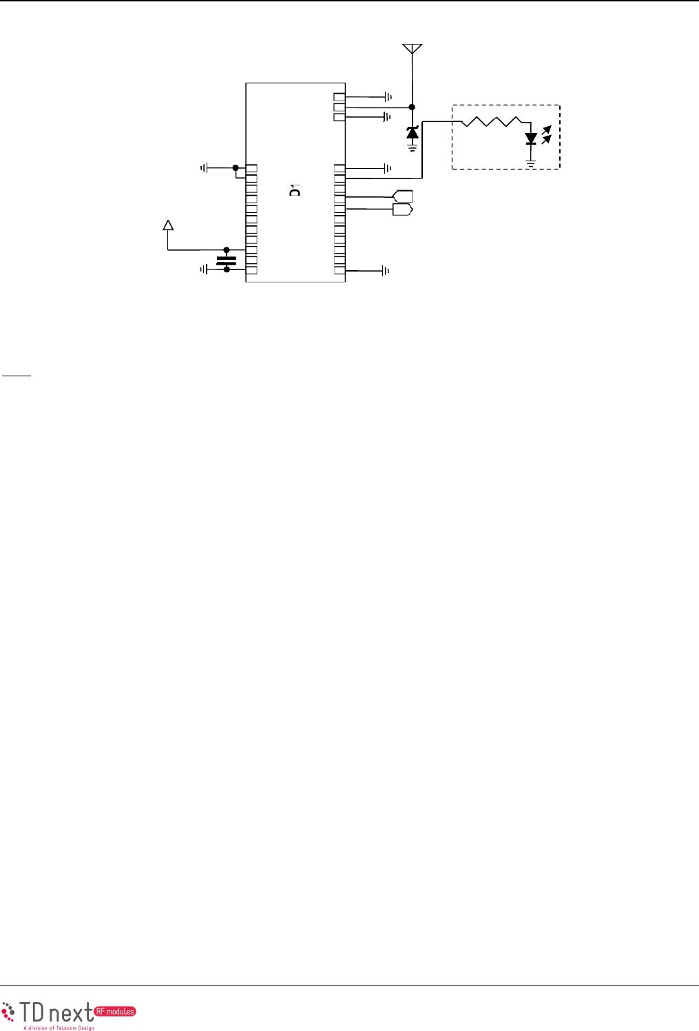
The application shown in Figure 1 shows the minimum interconnection required to operate the TD1508 module.
Basically, only the 5 GND, 2 RF_GND, V
DD
, TX, RX and RF antenna pin connections are necessary. The RST
(reset) pin connection is not mandatory and this pin can be left floating if not used.
A 10 µF/6.3V decoupling capacitor must be added as close as possible to the V
DD
pin.
The TX/RX pins are LVTTL-compatible and feature internal pull-up resistors.
A 50 Ω matched RF antenna must be connected to the RF pin, with a low-capacitance (< 0.5 pF) TVS diode to
protect the RF input from ESD transients.
The connection of a super-blue LED with series current-limiting resistor of 220 Ω on pin TIM2 is recommended in
order to display the bootloader status at boot time.
TD1508
Rev 1.4 (07/16) 17
Note: The TVS diode used for protecting the RF input against ESD must be of low-capacitance (0.5 pF typical) type,
e.g. ESD9R3.3ST5G (On Semiconductor), for example.
TD1508
2
1
4
3
6
5
8
7
10
9
11
2
1
22
19
20
17
18
15
16
13
14
12
2
4
25
23
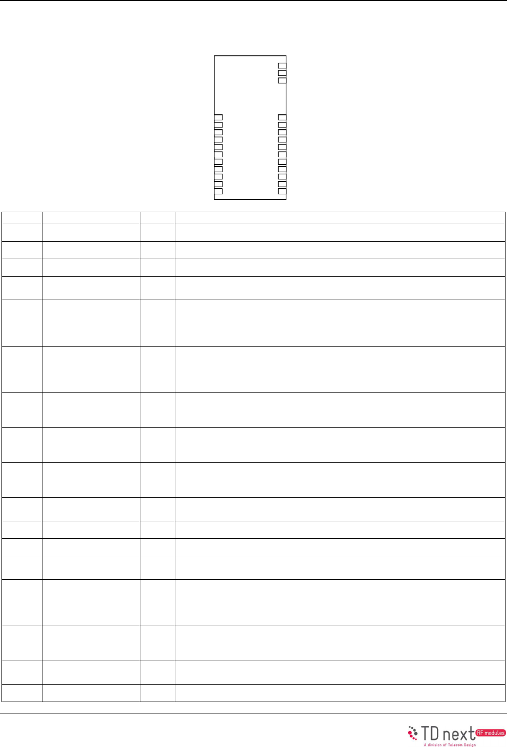
GND
GND
Reserved
USR4
DB3
DB2
SDA
SCL
VDD
USR2
GND
GND
USR3
RST
DAC0
USR0
USR1
TX
RX
ADC0
TIM2
GND
RF_GND
RF
RF_GND
TX
RX
VDD
10 µF/6V3
50Ω Antenna
220 Ω
Blue
LED
Recommended for Bootloader status display
TVS
Diode
Figure 1. Typical Application

TD1508
18 Rev 1.4 (07/16)
3 Module Interface
3.1 Low-Power UART (Universal Asynchronous Receiver/Transmitter)
The TD1508 communicates with the host MCU over a standard asynchronous serial interface consisting of only 2
pins: TX and RX. The TX pin is used to send data from the TD1508 module to the host MCU, and the RX pin is
used to receive data into the TD1508 module coming from the host MCU.
This interface allows two-way UART communication to be performed in low energy modes, using only a few µA
during active communication and only 150 nA when waiting for incoming data.
This serial interface is designed to operate using the following serial protocol parameters:
LVTTL electrical level
9600 bps
8 data bits
1 stop bit
No parity
No hardware/software flow control
This interface operates using LVTTL signal levels to satisfy the common interface to a low power host MCU. If an
EIA RS232-compliant interface voltage level is required, an RS232 level translator circuit must be used. It is also
possible to use a common USB/UART interface chip to connect to an USB bus.
Over this serial interface, the TD1508 device provides a standard Hayes “AT” command set used to control the
module using ASCII readable commands and get answers, as well as to send or receive data.
The list of available commands with their corresponding arguments and return values, a description of their
operation and some examples are detailed into the “TD1508 Reference Manual”.
3.2 USART (Universal Synchronous/Asynchronous Receiver/Transmitter)
The TD1508 provides an interface to an integrated USART capable of both asynchronous (UART and SmartCard)
or synchronous (SPI and I2S) communications. All modes benefit from 2-level buffers with additional separate shift
registers, configurable number of data bits and programmable bit endianess and baudrate.
Asynchronous mode allows both full and half-duplex operation with parity check/generation, parity and framing error
detection and Break condition detection. Synchronous mode is capable of acting as an SPI master or slave,
supporting all 4 SPI clock polarity/phase configurations.
The USART is available on pins USR1, USR2, USR3 and USR4. When not used for timer/counter operation, these
pins can be configured to perform other functions using “AT” configuration commands, please refer to the “TD1508
Reference Manual” for details.
3.3 I
2
C bus
As a convenience, the TD1508 module is equipped with a popular I
2
C serial bus controller that enables
communication with a number of external devices using only two I/O pins: SCL and SDA (alternatively, the DB2 and
DB3 pins can be configured as SCL and SDA, resprectively). The SCL pin is used to interface with the I
2
C clock
signal, and the SDA pin to the I
2
C data signal, respectively. When not used for I2C bus, these 2 pins can be
configured to perform other functions using “AT” configuration commands, please refer to the “TD1508 Reference
Manual” for details.
The TD1508 module is capable of acting as both a master and a slave, and supports multi-master buses. Both
standard-mode (Sm), fast-mode (Fm) and fast-mode plus (Fm+) speeds are supported, allowing transmission rates
all the way from 10 kbit/s up to 1 Mbit/s. Slave arbitration and timeouts are also provided to allow implementation

TD1508
Rev 1.4 (07/16) 19
of an SMBus compliant system. Both 7-bit and 10-bit addresses are supported, along with extensive error handling
capabilities (clock low/high timeouts, arbitration lost, bus error detection).
The operation of this interface is controlled by the mean of Hayes “AT” commands sent over the UART interface.
To obtain a list of the available commands with their corresponding arguments and return values, a description of
their operation and some examples, please refer to the “TD1508 Reference Manual”.
3.4 Timer/Counter
The TD1508 provides an interface to an integrated low-power timer/counter using the TIM2 pin. This pin can be
configured as either a capture input or a compare/PWM output to the 16-bit internal timer/counter. When not used
for timer/counter operation, this pin can be configured to perform other functions using “AT” configuration
commands, please refer to the “TD1508 Reference Manual” for details.
The low-power timer consists in a counter that can be configured to up-count, down-count, up/down-count
(continuous or one-shot).
The low-power timer also contains 2 output channels, that can be configured as either an output compare or
single/double slope PWM (Pulse-Width Modulation) outputs routed to the TIM2 pin.
The operation of this interface is controlled by the mean of Hayes “AT” commands sent over the UART interface.
To obtain a list of the available commands with their corresponding arguments and return values, a description of
their operation and some examples, please refer to the “TD1508 Reference Manual”.
3.5 ADC (Analog to Digital Converter)
The TD1508 provides an interface to an integrated low-power SAR (Successive Approximation Register) ADC,
capable of a resolution of up to 12 bits at up to 1 Msps or 6 bits at up to 1.86 Msps. The ADC0 pin provides the
external interface to the ADC. When not used for ADC operation, this pin can be configured to perform other
functions using “AT” configuration commands, please refer to the “TD1508 Reference Manual” for details.
Along with the ADC0 analog input channel, the ADC also provides an internal temperature, VDD, and GND input
channel that may be used to get a digital representation of analog temperature or voltage values. It is also possible
to loopback the analog output of the integrated DAC (see section 3.6, “DAC (Digital to Analog Converter)”).
The internal ADC provides an optional input filter consisting of an internal low-pass RC filter or simple internal
decoupling capacitor. The resistance and capacitance values are given in the electrical characteristics for the
device, named R
ADCFILT
and C
ADCFILT
respectively.
The reference voltage used by the ADC can be selected from several sources, including a 1.25 V internal bandgap,
a 2.5 V internal bandgap, V
DD
, a 5 V internal differential bandgap or unbuffered 2V
DD
.
Additionally, to achieve higher accuracy, hardware oversampling can be enabled. With oversampling, each selected
input is sampled a number of times, and the results are filtered by a first order accumulate and dump filter to form
the end result. Using 16x oversampling minimum, it is thus possible to achieve result resolution of upt to 16 bits.
The operation of this interface is controlled by the mean of Hayes “AT” commands sent over the UART interface.
To obtain a list of the available commands with their corresponding arguments and return values, a description of
their operation and some examples, please refer to the “TD1508 Reference Manual”.
3.6 DAC (Digital to Analog Converter)
The TD1508 provides an interface to an integrated DAC that can convert a digital value to a fully rail-to-rail analog
output voltage with 12-bit resolution at up to 500 ksps. The DAC may be used for a number of different applications
such as sensor interfaces or sound output. The analog DAC output is routed to the DAC0 pin. When not used for
ADC operation, this pin can be configured to perform other functions using “AT” configuration commands, please
refer to the “TD1508 Reference Manual” for details.

TD1508
20 Rev 1.4 (07/16)
The reference voltage used by the DAC can be selected from several sources, including a 1.25 V internal bandgap,
a 2.5 V internal bandgap, or V
DD
.
The internal DAC provides support for offset and gain calibration, and contains an automatic sine generation mode
as well as a loopback output to the ADC (see section 3.5, “ADC (Analog to Digital Converter)”).
3.7 GPIO (General Purpose Input/Output)
Apart from the TX and RX UART pins, and the RF pins, all signal pins are available as general-purpose
inputs/outputs. This includes of course the generic USR0, USR1, USR2, US3 and USR4 pins, but also the ADC0,
TIM2, DAC0, SCL, SDA, DB2, DB3 pins when not used for their main function. This configuration can be performed
using “AT” commands, please refer to the “TD1508 Reference Manual” for details.
All the USR0, USR1, USR2, USR3, USR4, ADC0, TIM2, DAC0, SCL, SDA, DB2, DB3 pins can be configured
individually as tristate (default reset state), push-pull, open-drain, with/without pull-up or pull-down resistor, and with
a programmable drive strength (0.5 mA/2 mA/6 mA/20 mA).
When configured as inputs, these pins feature an optional glitch suppression filter and full (rising, falling or both
edges) interrupt with wake-up from low-power mode capabilities. Of course, the pin configuration is retained even
when using these low-power modes.
The operation of the GPIOs is controlled by the mean of Hayes “AT” commands sent over the UART interface. To
obtain a list of the available commands with their corresponding arguments and return values, a description of their
operation and some examples, please refer to the “TD1508 Reference Manual”.
3.8 RST (Reset)
The TD1508 module features an active-low RST pin. This pin is held high by an internal pull-up resistor, so when
not used, this pin can be left floating.
3.9 Debug
The TD1508 module devices include hardware debug support through a 2-pin serial-wire debug interface. The 2
pins DB2 and DB3 are used for this purpose. The DB2 pin is the ARM Cortex-M3’s SWDIO Serial Wire data
Input/Output. This pin is enabled after a reset and has a built in pull-up. The DB3 pin is the ARM Cortex-M3’s
SWCLK Serial Wire Clock input. This pin is enabled after reset and has a built-in pull down. When not used for
debug operation, these 2 pins can be configured to perform other functions using “AT” configuration commands,
please refer to the “TD1508 Reference Manual” for details.
Additionally, the USR0, USR1 or USR2 pins can be used as the ARM Cortex-M3’s SWO Serial Wire viewer Output.
Note that this function is not enabled after reset, and must be enabled by software to be used.
Although the ARM Cortex-M3 supports advanced debugging features, the TD1508 devices only use two port pins
for debugging or programming. The systems internal and external state can be examined with debug extensions
supporting instruction or data access break- and watch points.
For more information on how to enable the debug pin outputs/inputs the reader is referred to Section 28.3.4.1 (p.
457), the ARM Cortex-M3 Technical Reference Manual and the ARM CoreSight™ Technical Reference Manual.
3.10 RF Antenna
The TD1508 support a single-ended RF pin with 50 Ω characteristic impedance for connecting a matched-
impedance external antenna. This pin is physically surrounded by 2 RF GND pins for better noise immunity.
3.11 VDD & GND
The TD1508 provides 5 GND pins and 2 RF_GND pins: all of them must be connected to a good ground plane.
A 10 µF/6.3 V decoupling capacitor should be placed as closed as possible to the single VDD pin.

TD1508
Rev 1.4 (07/16) 21
4 Bootloader
The TD1508 module contains an integrated bootloader which allows reflashing the module firmware either over the
RX/TX UART connection, or over the air using the built-in RF transceiver.
The bootloader is automatically activated upon module reset. Once activated, the bootloader will monitor the
UART/RF activity for a 200 ms period, and detect an incoming update condition.
If the update condition is met, the TD1508 will automatically proceed to flash the new firmware with safe retry
mechanisms, or falls back to normal operation.
TD1508
22 Rev 1.4 (07/16)
5 Pin Descriptions
Pin
Pin Name
I/O
Description
1 GND GND Connect to PCB ground
2 GND GND Connect to PCB ground
3 Reserved I/O Reserved pin – Do not connect
4 USR4 I/O
General Purpose Low
-
Power Digital I/O
This pin may be configured to perform various functions.
5 DB3 I
SWDCLK (SWD Clock) Signal
This signal provides the SWD clock signal to the integrated TD1508
ARM® CPU.
This pin may be configured to perform various functions.
6 DB2 I/O
SWDIO (SWD Data I/O) Signal
This signal provides the SWD programming/debugging signal interface to
the integrated TD1508 ARM® CPU.
This pin may be configured to perform various functions.
7 SDA I/O
General Purpose Low
-
Power Digital I/O
This pin may be configured to perform various functions, including the I
2
C
DATA (SDA) function.
8 SCL I/O
General Purpose Low
-
Power Digital I/O
This pin may be configured to perform various functions, including the I
2
C
clock (SCL) function.
9 VDD VDD
+2.3 to +3.3 V Supply Voltage Input
The recommended VDD supply voltage is +3.0V.
Connect a 10 µF capacitor as close as possible to this input.
10 USR2 I/O
General Purpose Low
-
Power Digital I/O
This pin may be configured to perform various functions.
11 GND GND Connect to PCB ground
12 GND GND Connect to PCB ground
13 USR3 I/O
General Purpose Low
-
Power Digital I/O
This pin may be configured to perform various functions.
14 RST I
Active Low RESET
input signal
This signal resets the TD1508 module to its initial state.
If not used, this signal can be left floating, as it is internally pulled up by
an integrated resistor.
15 DAC0 I/O
General Purpose Low
-
Power Digital I/O
This pin may be configured to perform various functions, including the
DAC analog output #0 function.
16 USR0 I/O
General Purpose Low
-
Power Digital I/O
This pin may be configured to perform various functions.
17 USR1 I/O General Purpose Low-Power Digital I/O
2
1
4
3
6
5
8
7
10
9
11
2
1
22
19
20
17
18
15
16
13
14
12
2
4
25
23
GND
GND
Reserved
USR4
DB3
DB2
SDA
SCL
VDD
USR2
GND
GND
USR3
RST
DAC0
USR0
USR1
TX
RX
ADC0
TIM2
GND
RF_GND
RF
RF_GND

TD1508
Rev 1.4 (07/16) 23
This pin may be configured to perform various functions.
18 TX O
Low
-
Power UART Data Transmit Signal
This signal provides the UART data going from the TD1508 module out
to the host application processor.
This signal is internally pulled up by an integrated resistor.
19 RX I
Lo
w
-
Power UART Data Receive Signal
This signal provides the UART data coming from the host application
processor going to the TD1508 module.
This signal is internally pulled up by an integrated resistor.
20 ADC0 I/O
General Purpose Low
-
Power Digital I/O
This pin may be configured to perform various functions, including the
ADC input #6 function.
21 TIM2 I/O
General Purpose Low
-
Power Digital I/O
This pin may be configured to perform various functions, including the
timer input capture / output compare #2 function.
22 GND GND Connect to PCB ground
23 RF_GND GND Connect to PCB ground
24 RF RF 50 Ω Antenna Connection
25 RF_GND GND Connect to PCB ground

TD1508
24 Rev 1.4 (07/16)
6 I/O alternate functionalities
Pin Name
Location
Description
Port
Bit
TX C 6
LEUART0 TX function.
Analog Comparator ACMP0, channel 6.
I
2
C bus 1 DATA (SDA) function.
LESENSE Channel 6.
RX C 7
L
EUART0 RX function.
Analog Comparator ACMP0, channel 7.
I
2
C bus 1 CLOCK (SCL) function.
LESENSE Channel 7.
DAC0 C 12
Digital to Analog Converter DAC0 output.
Analog comparator ACMP1, channel 4.
Operational Amplifier 1 alternate output.
UART 1 TX function.
USR0 C 15
An
alog C
omparator ACMP1, channel 7
.
Digital to Analog Converter DAC0 alternate output.
Operational Amplifier 1 alternate output.
Timer 1 Capture Compare input / output channel 2.
UART 0 RX function.
LESENSE Channel 15.
Debug-interface Serial Wire viewer output.
Note that this function is not enabled after reset, and
must be enabled by software to be used
USR4 D 0
Analog to digital conver
ter ADC0, input channel number 0.
Operational Amplifier 2 output.
Pulse Counter 2, input 0.
USART1 TX (MOSI) function.
USR2 D 1
Analog to digital conver
ter ADC0, input channel number 1.
Digital to Analog Converter DAC0 alternate output.
Operational Amplifier 1 alternate output.
Timer 0, input/output 0.
Pulse Counter 2, input 1.
USART1 RX (MISO) function.
Debug-interface Serial Wire viewer output.
Note that this function is not enabled after reset, and
must be enabled by software to be used
USR1 D 2
Analog to digital conver
ter ADC0, input channel number 2.
Timer 0, input/output 1.
USART1 Clock (CLK) function.
Debug-interface Serial Wire viewer output.
Note that this function is not enabled after reset, and
must be enabled by software to be used
USR3 D 3
Analog to digital conver
ter ADC0, input channel number 3.
Timer 0, input/output 2.
USART1 Chip Select (CS) function.
Debug-interface Serial Wire viewer output.
Note that this function is not enabled after reset, and
must be enabled by software to be used
ADC0 D 6
Analog to digital converter ADC0, input channel number 6
.
Operational Amplifier 1 positive input.
Timer 1, input/output 0.
LETIMER0, output 0.
Pulse Counter 0, input 0.
USART1 RX function.
I
2
C bus 0 DATA (SDA) function.
LESENSE Alternate Excite Channel 0.
Analog Comparator ACMP0 output.

TD1508
Rev 1.4 (07/16) 25
TIM2 D 7
LETIMER0, output 1
.
Analog to digital converter ADC0, input channel number 7.
Operational Amplifier 1 negative input.
Timer 1, input/output 1.
Pulse Counter 0, input 1.
USART1 TX function.
I
2
C bus 0 CLOCK (SCL) function.
CMU Clock output number 0.
LESENSE Alternate Excite Channel 1.
Analog Comparator ACMP1 output.
SDA E 0
I
2
C bus 0 DATA (SDA) function.
Timer 3, input/output 0.
Pulse Counter 0, input 0.
SCL E 1
I
2
C bus 0 CLOCK (SCL) function.
Timer 3, input/output 1.
Pulse Counter 0, input 1.
DB3 F 0
Debug
-
interface Serial Wire clock input.
Note that this function is enabled to pin out of reset, and has a
built-in pull-down
Timer 0, input/output 0.
LETIMER0 output number 0.
USART1 Clock (CLK) function.
LEUART0 TX function.
I
2
C bus 0 DATA (SDA) function.
DB2 F 1
Debug
-
interface Serial Wire data input / output.
Note that this function is enabled to pin out of reset, and has a
built-in pull up
Timer 0, input/output 1.
LETIMER0 output number 1.
USART1 Chip Select (CS) function.
LEUART0 RX function.
I
2
C bus 0 CLOCK (SCL) function.
Wake-up from EM4, pin number 3.

TD1508
26 Rev 1.4 (07/16)
7 Ordering Information
Part
Number
Description
Package Type
Operating
Temperature
TD1508-US US ISM SIGFOX™ gateway 128K
Flash/32KRAM TCXO LGA25
Pb-free -30° to +75°C
The TD1508-US ISM SIGFOX™ gateway module is available in several conditionings.
Please contact Telecom Design for more information.
TD1508
Rev 1.4 (07/16) 27
8 Package Outline
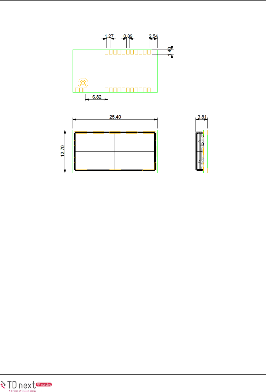
Figure 2 illustrates the package details for the TD1508.
Figure 2. 25-Pin Land Grid Array (LGA)
Notes:
1. All dimensions are shown in millimeters (mm) unless otherwise noted.
Bottom View
Top View
TD1508
28 Rev 1.4 (07/16)
9 PCB Land Pattern
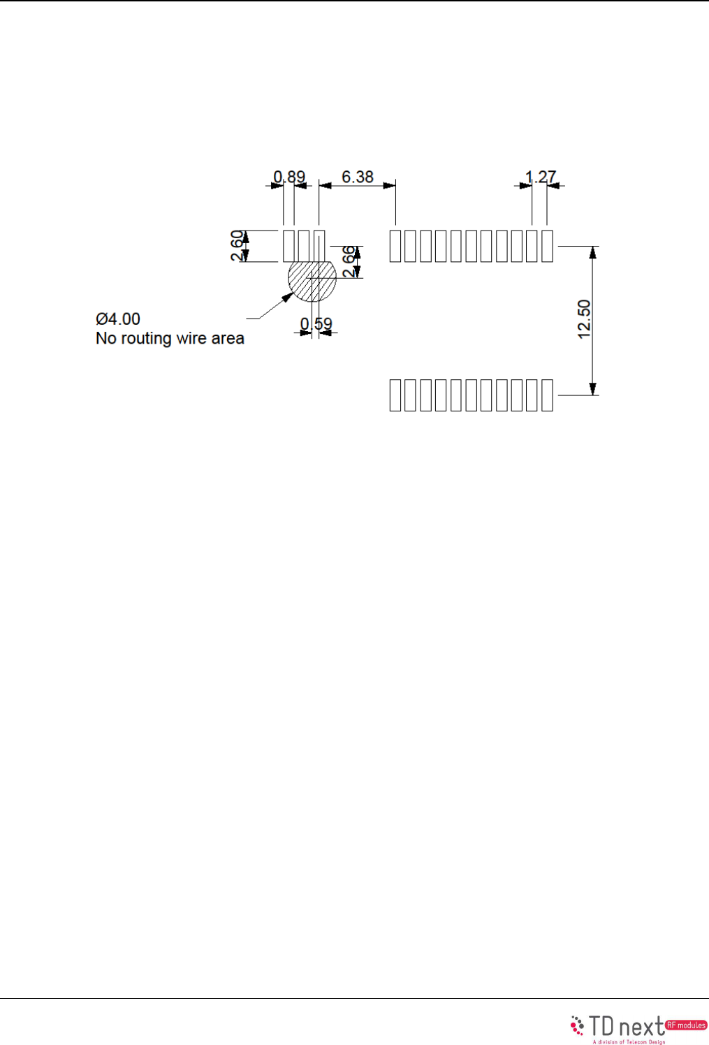
Figure 3 illustrates the PB land pattern details for the TD1508.
Figure 3. PCB Land Pattern
Notes:
1. All dimensions are shown in millimeters (mm) unless otherwise noted.
TD1508
Rev 1.4 (07/16) 29
10 Soldering Information
10.1 Solder Stencil
The TD1508 module is designed for RoHS reflow process surface mounting.
For proper module assembly, the solder paste must be applied on the receiving PCB using a metallic stencil with a
recommended 0.150 µm thickness.
10.2 Reflow soldering profile
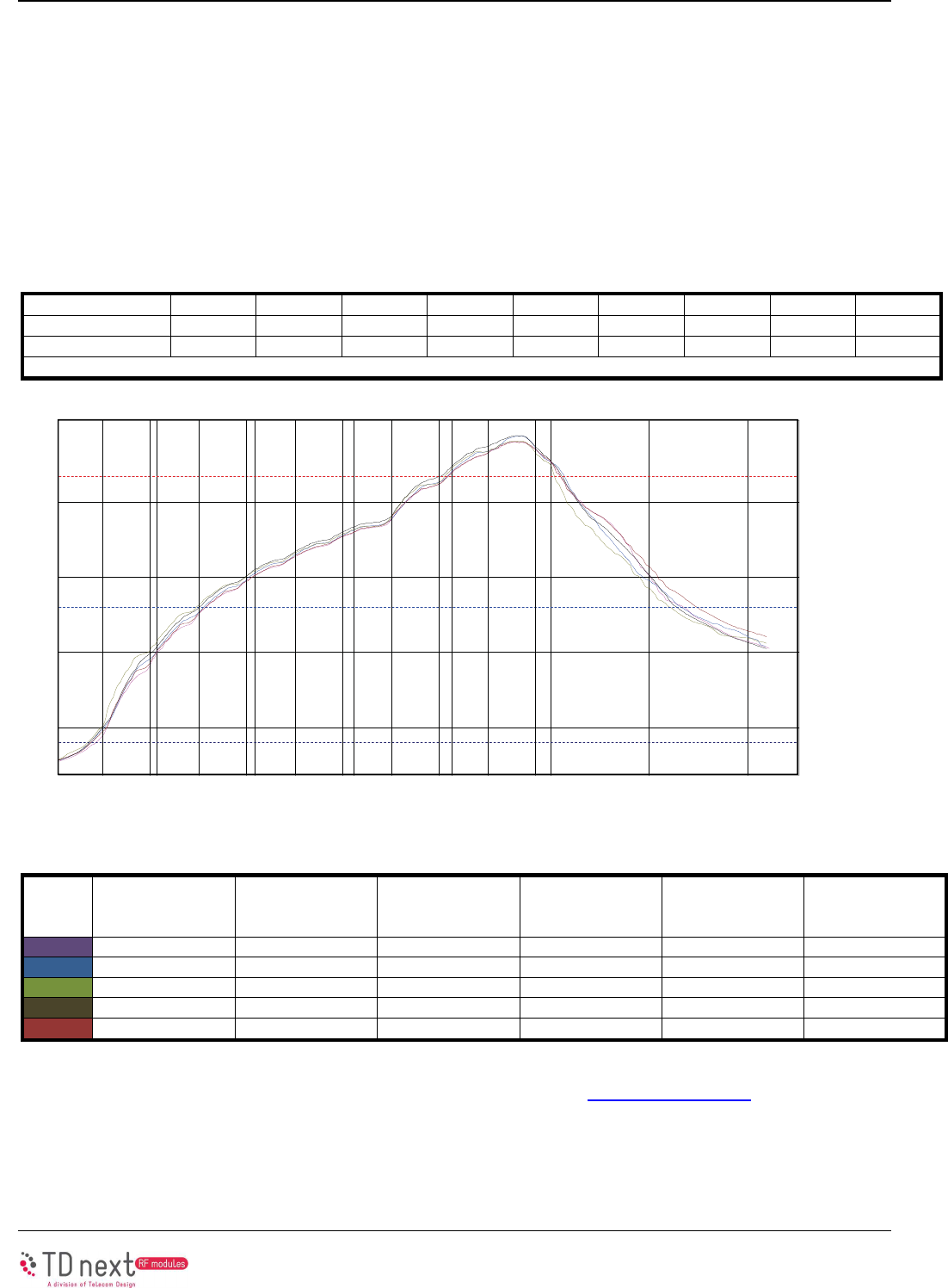
The recommendation for lead-free solder reflow from IPC/JEDEC J-STD-020D Standard should be followed.
Below are typical reflow soldering profiles for a medium-size board:
Setpoints
1
2
3
4
5
6
7
8
9
Top (°C) 145 155 165 175 185 195 230 250 250
Bottom (°C) 145 155 165 175 185 195 230 250 250
Notes:
Conveyor Speed is 65.00 cm / min
Figure 4 - Reflow Soldering Profile
Run
Preheat
(s)
40-130°C
Soak Time
(s)
130-217°C
Reflow Time
(s) / 217°C
Peak Temp
(°C)
Max.
Slope1
(°C / s)
(40-130°C)
Max.
Slope2
(°C / s)
(250-150°C)
2 56.04 122.40 58.66 239.00 1.53 -2.78
3 56.93 123.72 59.45 243.93 1.56 -2.79
4 55.34 124.25 57.34 239.45 1.54 -2.87
5 55.92 122.53 61.46 244.00 1.57 -2.77
6 58.12 123.38 57.89 239.84 1.53 -2.73
For more information on reflow soldering process profiling, please visit the http://kicthermal.com/ website.
0 50 100 150 200 250 300 350
Z1 Z2 Z3 Z4 Z5 Z6 Z7 Z8 Z9
50
100
150
200
Time (seconds)
Temperature (°C)
TD1508
30 Rev 1.4 (07/16)
11 Board Mounting Recommendation
11.1 Electrical Environment
The best TD1508 module performances are obtained in a “noise free” environment. Some basic recommendations
must be followed:
• Noisy electronic components (serial RS232, DC/DC Converter, Display, Ram, bus…) must be placed as far
as possible from the TD1508 module.
CAUTION – A particular attention must be put on switching power supply DC/DC converter, due to switching
frequency that generates spurious into the receiver band, as it can strongly decrease module
performances. Therefore it is recommended to put a metallic shield covering the DC/DC conversion
function.
• Switching component circuits (especially RS-232/TTL interface circuit power supply) must be decoupled
with a 100 µF low ESR tantalum capacitor. The decoupling capacitor must be placed as close as possible
to the noisy chip.
11.2 Power Supply Decoupling
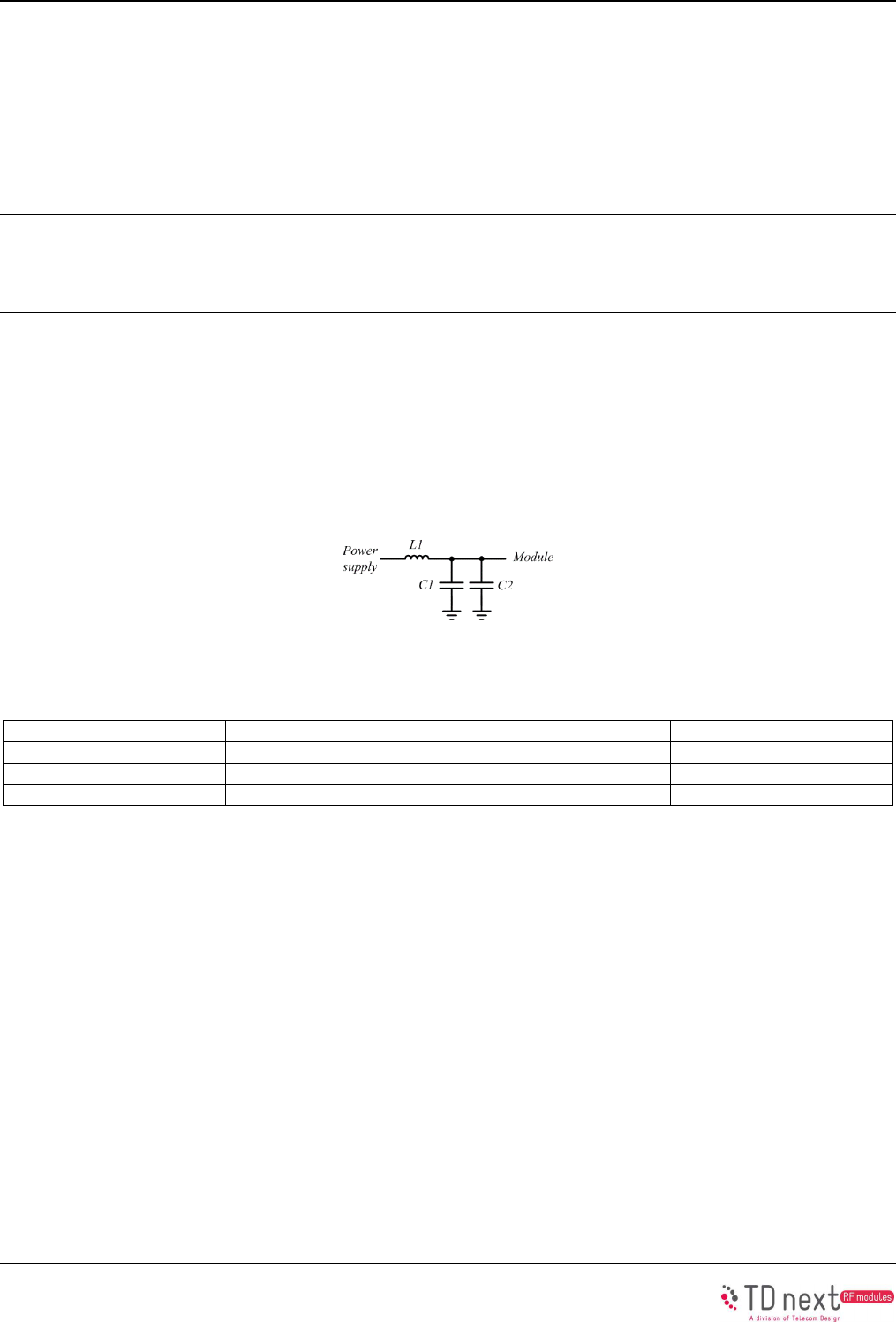
The power supply of the TD1508 module must be closely decoupled. An LC filter is strongly recommended in case
of a switching DC/DC power supply converter. It must be placed as close as possible to the TD1508 module power
supply pin VDD.
Figure 5- Power supply decoupling
For example:
Symbol Reference Value Manufacturer
L1 LQH32CN1R0M33 1 µH Murata
C1 GRM31CF51A226ZE01 22 µF Murata
C2 Ceramic CMS 25V 100 nF Multiple
11.3 RF Layout Considerations
Basic recommendations must be followed to achieve a good RF layout:
• It is recommended to fill all unused PCB area around the module with ground plane
• The radio module ground pins must be connected to a solid ground plane
• If the ground plane is on the bottom side, a via (metal hole) must be used in front of each ground pad.
Especially pins 23 and 25 (RF_GND) pins should be grounded via several holes to be located right next to
the pins, thus minimizing inductance and preventing mismatch and losses
11.4 Host Antenna Circuit Trace Design
11.4.1 Filter and Matching
This block has 2 purposes:
1. Filter the RF signal, especially harmonic 2 (H2) in transmit mode
2. Match antenna impedance to 50 Ω
TD1508
Rev 1.4 (07/16) 31
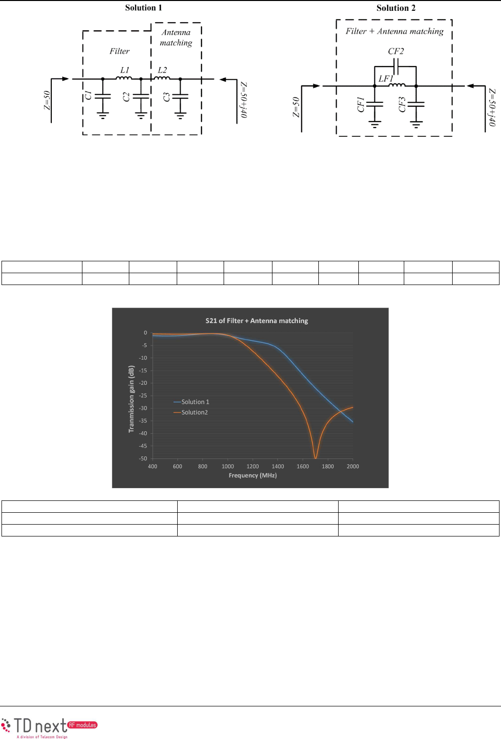
The proposed filter network is designed in order to match and filter with optimal performances while requiring the
minimum number of passive components (Figure 7).
For an example antenna featuring a (50+j*40) Ω impedance that must be filtered and matched to the 50 Ω TD1508
module impedance, the tables and graphics below summarize the component values used in order to present a
(50-j*40)Ω impedance at antenna connection with a good H2 rejection and the corresponding transmission gains:
Component C1 L1 C2 L2 C3 CF1 CF2 LF1 CF3
Value 4.7pF 9.1nH 4.7pF 8.2nH 3.3pF 3pF 1pF 8.2nH 4.7pF
S21 (dB) Solution 1 Solution 2
@ 868MHz -0.37 -0.32
@1736MHz -23.7 -42.8
11.4.2 RF Reference Layout
In order to get the best performance while meeting the electromagnetic interference standard requirements, the RF
trace geometric characteristics and passive component placement must be controlled, such that the RF signal
traces are surrounded by a solid ground plane and the RF signal traces matched to the 50 Ω impedance.
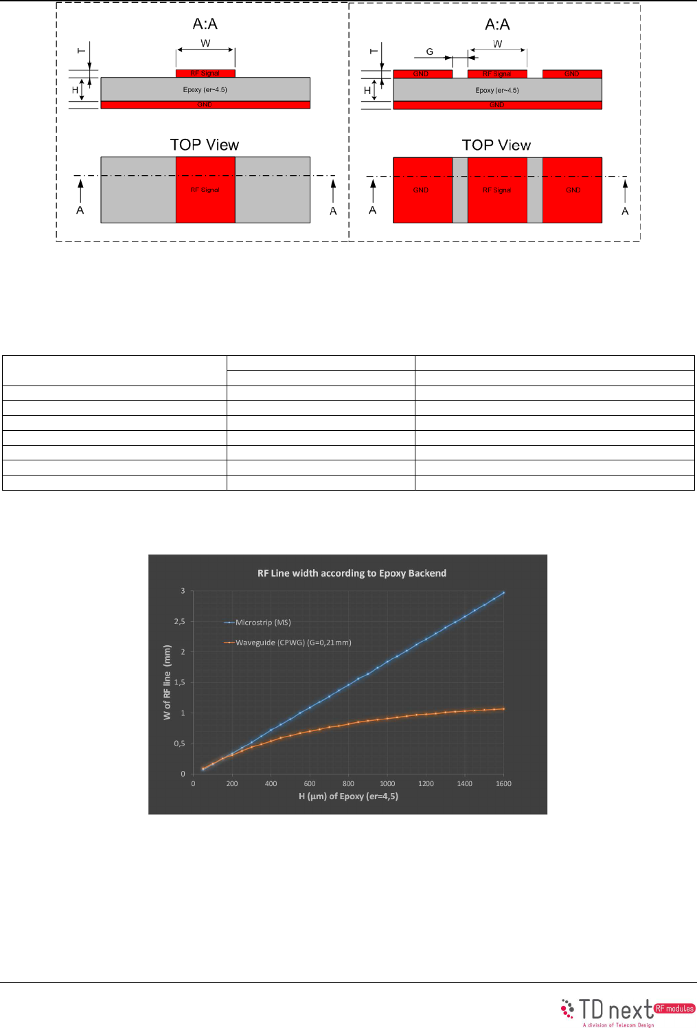
The 2 most common trace topologies used are the Microstrip and Coplanar Waveguide with lower ground
configurations, which are illustrated in figures 8 and 9 below:
Figure 6 - Classic filter architecture Figure 7 - Proposed filter architecture
TD1508
32 Rev 1.4 (07/16)
Figure 8- Microstrip Line (MS) Figure 9 Lower Ground Waveguide (CPWG)
The table below provides the recommended trace width to obtain 50 Ω impedance for RF traces on an PCB stack
up (Prepreg) having an εr = 4.5. For the CPWG solution, the proposed clearance between the RF signal and
ground is chosen to be 0.21 mm.
H (µm) MS CPWG (G=0.21mm)
W (mm) W (mm)
150 0.254 0.254
250 0.43 0.38
350 0.6 0.5
450 0.81 0.59
550 1 0.67
1200 2.21 0.98
1600 2.97 1.07
Figure 10 provides more details on the required trace width relative to the Epoxy thickness (H):
Figure 10- RF trace width relative to Epoxy stackup thickness
As can be observed, the MS trace width is wider and more dependent on H than the CPWG trace width:
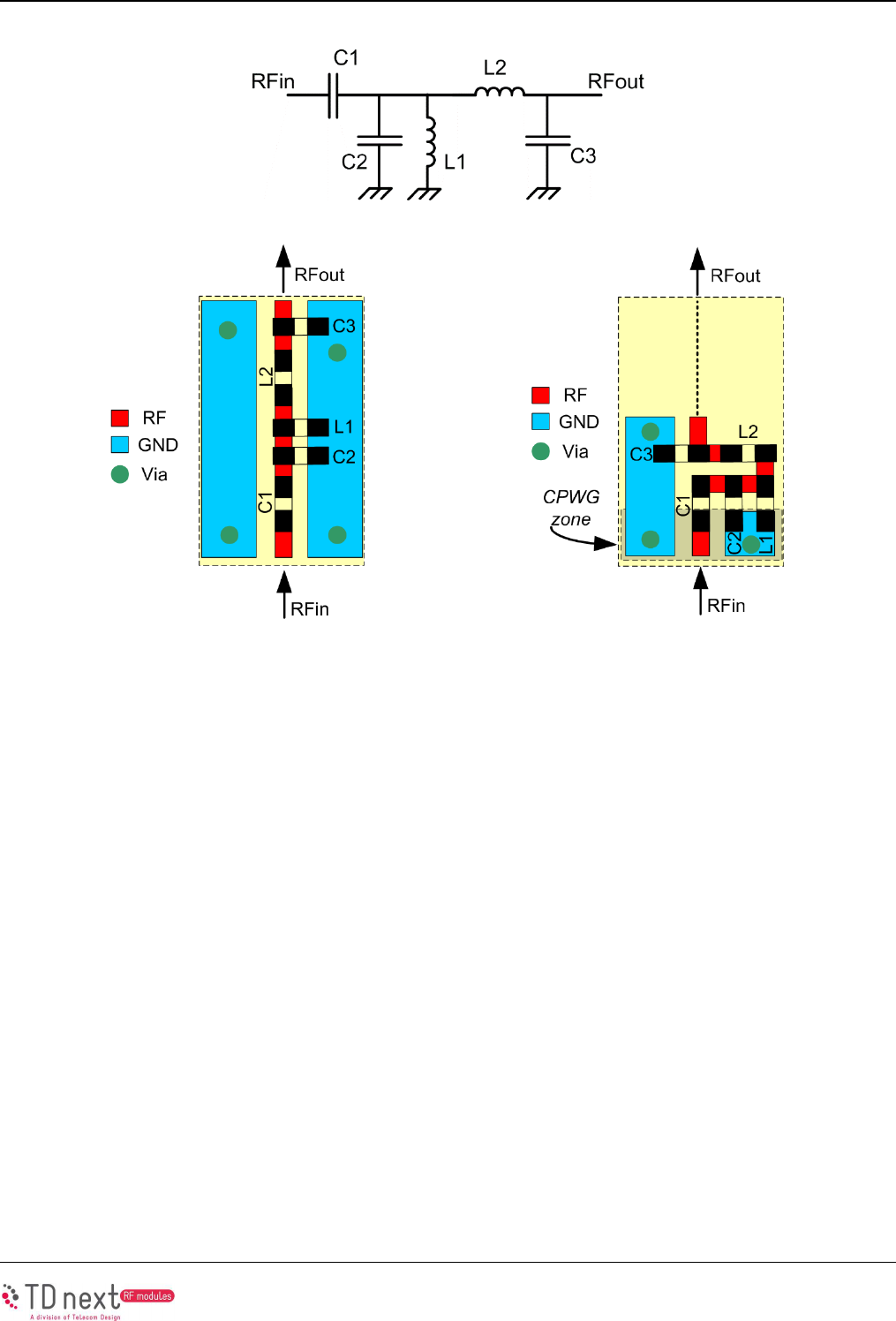
However, because of the increasing demand to downscale circuits, the MS solution allows to increase the
component and trace density, see Figure 11 below:
TD1508
Rev 1.4 (07/16) 33
a) Example matching network schematic
b) CPWG layout c) MS layout
Figure 11- Impact of RF trace topology choice on board real-estate
Nevertheless, several RF matching network components must be connected to GND, creating a parasitic CPWG
area in the MS configuration (e.g. gray area in MS layout). In order to limit the influence of this area, H must be kept
thin (< 400µm), such that the width of MS and CPWG traces are similar and achieve the same 50 Ω impedance (cf.
Figure 10). It is also possible to update the RF signal to GND clearance value (G) for CPWG in order to get the
same impedance with the same trace width between MS and CPWG configurations.
The quality of the ground plane is essential for a good RF performance. Several vias must be placed in order to
connect together (“stitch”) the grounds (top layer and internal layer) and to avoid a parasitic antenna phenomenon
or voltage level differences over the overall circuit ground. However, too numerous via holes may weaken the FR4
mechanical properties, so there should not be too many of them in order to avoid any side effects and decrease the
circuit reliability.
TD1508
34 Rev 1.4 (07/16)
11.4.3 Proposed PCB Stack-Up for combined MS / CPWG RF Traces
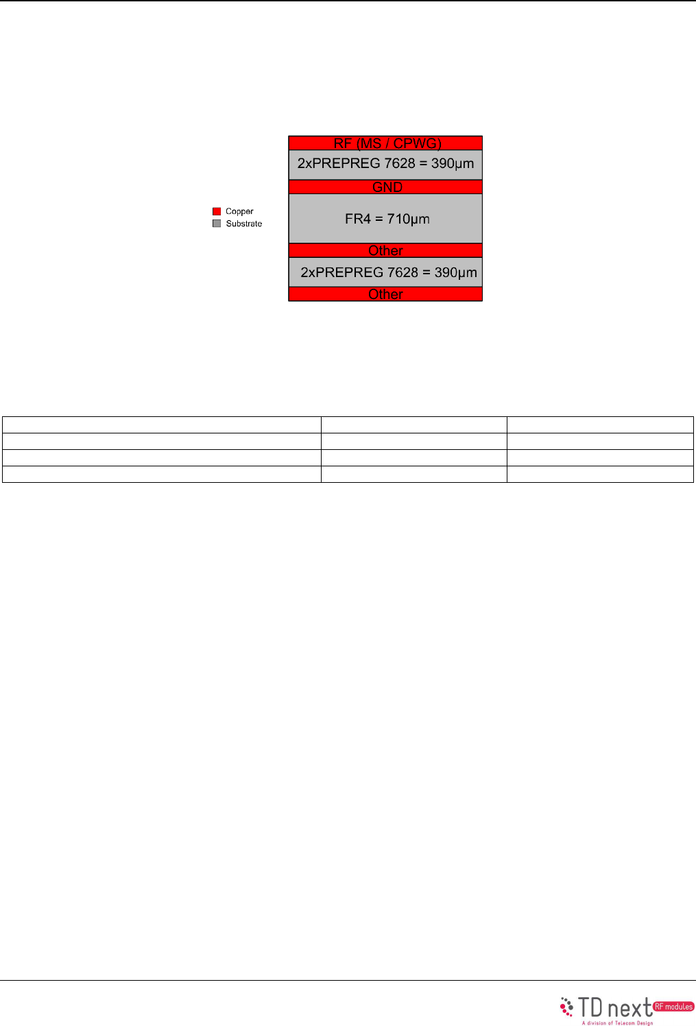
The proposed PCB stack-up is depicted in Figure 12. This stack-up is made up of 4 copper layers with a total
thickness of about 1.6 mm. The core FR4 thickness can be modified in order to reach a total thickness of 1.2 mm.
Figure 12- Proposed PCB stack-up
The width (W) of RF traces is fixed to 0.6 mm (matching 0402 component footprints), with a clearance (G) of 0.35
mm. These values allow to cancel the 0402 footprint impact on the RF matching. The table below provides the
expected minimum and maximum RF trace impedances relative to the PREPREG tolerances:
2xPREPREG 7628 Impedance of MS (Ω) Impedance of CPWG (Ω)
(-40 µm) => 350 µm 51.3 48.9
(+0 µm) => 390 µm 54.6 51.3
(+40 µm) => 430 µm 57.6 53.3
TD1508
Rev 1.4 (07/16) 35
12 Conformity Assessment Issues / FCC Regulatory Notices
12.1 Modification Statement
Telecom Design S.A. does not approve any changes or modifications to this device by the user. Any changes or
modifications could void the user’s authority to operate the equipment.
12.2 Interference Statement
This device complies with Part 15 of the FCC Rules.
Operation is subject to the following two conditions:
(1) This device may not cause harmful interference, and
(2) This device must accept any interference received, including interference that may cause undesired
operation.
12.3 Wireless Notice
This equipment complies with FCC radiation exposure limits set forth for an uncontrolled environment. This
equipment should be installed and operated with a minimum distance of 20 cm between the radiator and your
body.
Antenna gain and type must be:
Type Maximum Gain
λ/2 dipole antenna 2 dBi
This transmitter must not be co-located or operating in conjunction with any other antenna or transmitter.
12.4 FCC Class B Digital Device Notice
This equipment has been tested and found to comply with the limits for a Class B digital device, pursuant to Part 15
of the FCC Rules. These limits are designed to provide reasonable protection against harmful interference in a
residential installation. This equipment generates, uses and can radiate radio frequency energy and, if not installed
and used in accordance with the instructions, may cause harmful interference to radio communications. However,
there is no guarantee that interference will not occur in a particular installation. If this equipment does cause harmful
interference to radio or television reception, which can be determined by turning the equipment off and on, the user
is encouraged to try to correct the interference by one or more of the following measures:
• Reorient or relocate the receiving antenna.
• Increase the separation between the equipment and receiver.
• Connect the equipment into an outlet on a circuit different from that to which the receiver is connected.
Consult the dealer or an experienced radio/TV technician for help.
12.5 Labelling Requirements for the Host Device
The host device shall be properly labelled to identify the modules within the host device. The certification label of
the module shall be clearly visible at all times when installed in the host device, otherwise the host device must be
labelled to display the FCC ID of the module, preceded by the words "Contains transmitter module", or the word
"Contains", or similar wording expressing the same meaning, as follows:
Contains FCC ID: 2AGMK-TD1508

TD1508
36 Rev 1.4 (07/16)
D
OCUMENT
C
HANGE
L
IST
Revision 1.0
First Release
Revision 1.1
Remove the 25dBm output configuration
Change TX power consumption
Revision 1.2
Added FCC and IC warning statements
Revision 1.3
Removed IC warning statements
Added Board Mounting Recommendation
Added Conformity Assessment Issues / FCC Regulatory Notices
Revision 1.4
Corrected minimal distance unit

TD1508
Rev 1.4 (07/16) 37
N
OTES
:

TD1508
38 Rev 1.4 (07/16)
C
ONTACT
I
NFORMATION
Telecom Design S.A.
Zone Actipolis II — 2 bis rue Nully de Harcourt
33610 CANEJAN, France
Tel: +33 5 57 35 63 70
Fax: +33 5 57 35 63 71
Please visit the Telecom Design web page:
http://www.telecomdesign.fr/
The information in this document is believed to be accurate in all respects at the time of publication but is subject to change without notice.
Telecom Design assumes no responsibility for errors and omissions, and disclaims responsibility for any consequences resulting from the use
of information included herein. Additionally, Telecom Design assumes no responsibility for the functioning of undescribed features or parameters.
Telecom Design reserves the right to make changes without further notice. Telecom Design makes no warranty, representation or guarantee
regarding the suitability of its products for any particular purpose, nor does Telecom Design assume any liability arising out of the application or
use of any product or circuit, and specifically disclaims any and all liability, including without limitation consequential or incidental damages.
Telecom Design products are not designed, intended, or authorized for use in applications intended to support or sustain life, or for any other
application in which the failure of the Telecom Design product could create a situation where personal injury or death may occur. Should Buyer
purchase or use Telecom Design products for any such unintended or unauthorized application, Buyer shall indemnify and hold Telecom Design
harmless against all claims and damages.
Telecom Design is a trademark of Telecom Design S.A.
SIGFOX™ is a trademark of SigFox S.A.
Other products or brand names mentioned herein are trademarks or registered trademarks of their respective holders.